JP5199010B2 - RFID tag manufacturing method and RFID tag - Google Patents
RFID tag manufacturing method and RFID tag Download PDFInfo
- Publication number
- JP5199010B2 JP5199010B2 JP2008255891A JP2008255891A JP5199010B2 JP 5199010 B2 JP5199010 B2 JP 5199010B2 JP 2008255891 A JP2008255891 A JP 2008255891A JP 2008255891 A JP2008255891 A JP 2008255891A JP 5199010 B2 JP5199010 B2 JP 5199010B2
- Authority
- JP
- Japan
- Prior art keywords
- sheet
- sheet member
- base substrate
- circuit chip
- chip
- Prior art date
- Legal status (The legal status is an assumption and is not a legal conclusion. Google has not performed a legal analysis and makes no representation as to the accuracy of the status listed.)
- Expired - Fee Related
Links
Images


Classifications
-
- G—PHYSICS
- G06—COMPUTING; CALCULATING OR COUNTING
- G06K—GRAPHICAL DATA READING; PRESENTATION OF DATA; RECORD CARRIERS; HANDLING RECORD CARRIERS
- G06K19/00—Record carriers for use with machines and with at least a part designed to carry digital markings
- G06K19/06—Record carriers for use with machines and with at least a part designed to carry digital markings characterised by the kind of the digital marking, e.g. shape, nature, code
- G06K19/067—Record carriers with conductive marks, printed circuits or semiconductor circuit elements, e.g. credit or identity cards also with resonating or responding marks without active components
- G06K19/07—Record carriers with conductive marks, printed circuits or semiconductor circuit elements, e.g. credit or identity cards also with resonating or responding marks without active components with integrated circuit chips
- G06K19/077—Constructional details, e.g. mounting of circuits in the carrier
- G06K19/07749—Constructional details, e.g. mounting of circuits in the carrier the record carrier being capable of non-contact communication, e.g. constructional details of the antenna of a non-contact smart card
-
- G—PHYSICS
- G06—COMPUTING; CALCULATING OR COUNTING
- G06K—GRAPHICAL DATA READING; PRESENTATION OF DATA; RECORD CARRIERS; HANDLING RECORD CARRIERS
- G06K19/00—Record carriers for use with machines and with at least a part designed to carry digital markings
- G06K19/06—Record carriers for use with machines and with at least a part designed to carry digital markings characterised by the kind of the digital marking, e.g. shape, nature, code
- G06K19/067—Record carriers with conductive marks, printed circuits or semiconductor circuit elements, e.g. credit or identity cards also with resonating or responding marks without active components
- G06K19/07—Record carriers with conductive marks, printed circuits or semiconductor circuit elements, e.g. credit or identity cards also with resonating or responding marks without active components with integrated circuit chips
- G06K19/077—Constructional details, e.g. mounting of circuits in the carrier
- G06K19/07718—Constructional details, e.g. mounting of circuits in the carrier the record carrier being manufactured in a continuous process, e.g. using endless rolls
-
- Y—GENERAL TAGGING OF NEW TECHNOLOGICAL DEVELOPMENTS; GENERAL TAGGING OF CROSS-SECTIONAL TECHNOLOGIES SPANNING OVER SEVERAL SECTIONS OF THE IPC; TECHNICAL SUBJECTS COVERED BY FORMER USPC CROSS-REFERENCE ART COLLECTIONS [XRACs] AND DIGESTS
- Y10—TECHNICAL SUBJECTS COVERED BY FORMER USPC
- Y10T—TECHNICAL SUBJECTS COVERED BY FORMER US CLASSIFICATION
- Y10T29/00—Metal working
- Y10T29/49—Method of mechanical manufacture
- Y10T29/49002—Electrical device making
- Y10T29/49016—Antenna or wave energy "plumbing" making
Landscapes
- Engineering & Computer Science (AREA)
- Computer Hardware Design (AREA)
- Microelectronics & Electronic Packaging (AREA)
- Physics & Mathematics (AREA)
- General Physics & Mathematics (AREA)
- Theoretical Computer Science (AREA)
- Credit Cards Or The Like (AREA)
Description
本発明は、外部装置との間で非接触で通信する回路チップを備えたRFIDタグの製造方法、およびそのRFIDタグに関する。 The present invention relates to a method of manufacturing an RFID tag including a circuit chip that performs non-contact communication with an external device, and the RFID tag.
近年、非接触で外部との情報の受け渡しが可能なIC(Integrated Circuit)チップが注目されている。例えば、このような非接触型のICチップがカード基材の内部に設けられたICカードは、電子マネー、交通機関の定期券、入館証などに広く利用されている。 In recent years, IC (Integrated Circuit) chips capable of exchanging information with the outside without contact have been attracting attention. For example, an IC card in which such a non-contact type IC chip is provided inside a card substrate is widely used for electronic money, transportation commuter pass, admission card and the like.
また、このようなICチップにIDを記憶させ、商品などの識別や管理に利用することが考えられている。このような用途の非接触ICチップは、RFID(Radio Frequency ID)タグなどと呼ばれる。RFIDタグは、一般的に、読み取り器からの電波あるいは電磁波を基に駆動電力を発生し、読み取り器と無線通信して、ICチップのメモリ内に記憶されたIDなどの情報を読み取り器に送信する。また、RFIDタグには、ICチップのメモリへの書き込みが可能なものや、外部装置との間の認証処理など、受信した情報や記憶している情報を用いた各種の処理を実行できるものもある。 In addition, it is considered that an ID is stored in such an IC chip and used for identification and management of products. The non-contact IC chip for such a use is called an RFID (Radio Frequency ID) tag. An RFID tag generally generates drive power based on radio waves or electromagnetic waves from a reader, wirelessly communicates with the reader, and transmits information such as an ID stored in an IC chip memory to the reader. To do. In addition, some RFID tags can write to the IC chip memory, and others can execute various processes using received information and stored information, such as authentication processing with external devices. is there.
ところで、非接触型ICチップを搭載したICカードには、樹脂製のカード基材の間に、ICチップや通信用のアンテナなどが設けられた構造のものが多い。また、このようなICカードでは、機械的強度を高めるために、金属などの補強部材によってICチップの両面を挟む構造としたものがある(例えば、特許文献1参照)。さらに、ICチップの主面側に、チップの電極に対応する部分が開口した補強板を直接接合するようにして、ICカードを薄型化することも考えられている(例えば、特許文献2参照)。また、ICチップやコイルなどを搭載したモジュールパッケージとカード基材との間に、補強材として繊維材を設けたものもある(例えば、特許文献3参照)。 By the way, many IC cards equipped with a non-contact type IC chip have a structure in which an IC chip, a communication antenna, and the like are provided between resin card bases. Some IC cards have a structure in which both sides of an IC chip are sandwiched between reinforcing members such as metal in order to increase mechanical strength (see, for example, Patent Document 1). Further, it is also considered to make the IC card thinner by directly joining a reinforcing plate having an opening corresponding to the electrode of the chip to the main surface side of the IC chip (see, for example, Patent Document 2). . In some cases, a fiber material is provided as a reinforcing material between a module package on which an IC chip, a coil, or the like is mounted and a card substrate (see, for example, Patent Document 3).
一方、RFIDタグも、一般的に、ICチップが通信用のアンテナなどと一体にモジュール化された形態で提供される。そして、このようなRFIDタグでも、折り曲げなどに対する強度を高めることが要求されている。さらに、RFIDタグを衣服などに取り付ける用途も想定されており、このようなものでは液体や薬剤に対する耐性も求められている。そこで、RFIDタグを、補強部材をICチップに積層するとともに、このようなICチップが搭載されたモジュールを保護シートにより封止することによって製造することが考えられている。
しかし、補強部材を配し、保護シートで内部回路を封止したRFIDタグの製造には、製造に手間がかかり、製造コストが増大してしまうという問題があった。
例えば、RFIDタグを製造する際には、あらかじめアンテナパターンを形成したシート状の基板自体は、ロールなどに巻き付けが可能な程度の厚みで用意しておくことができる。しかし、このシート状基板に対してICチップを取り付け、その上に補強部材を実装した場合、ICチップおよび補強部材の双方は曲げ抵抗が大きいため、シート状基板を再度ロールで巻き取ることが困難になる。このため、例えば、シート状基板を1つまたは複数のICチップを単位として切断した後、保護シートによる封止工程をバッチ処理で行う必要が生じる。このように、フィルム基板をロールに巻き付けた状態のまま、補強部材や保護シートを連続的に積層することができない場合には、低コストで大量に生産することが難しくなる。
However, the production of an RFID tag in which a reinforcing member is arranged and an internal circuit is sealed with a protective sheet has a problem that it takes time and effort to increase the production cost.
For example, when manufacturing an RFID tag, a sheet-like substrate itself on which an antenna pattern is formed in advance can be prepared with a thickness that can be wound around a roll or the like. However, when an IC chip is attached to this sheet-like substrate and a reinforcing member is mounted thereon, it is difficult to wind the sheet-like substrate again with a roll because both the IC chip and the reinforcing member have high bending resistance. become. For this reason, for example, after cutting the sheet-like substrate in units of one or a plurality of IC chips, it is necessary to perform a sealing process with a protective sheet by batch processing. Thus, when a reinforcing member and a protection sheet cannot be laminated | stacked continuously in the state which wound the film substrate around the roll, it becomes difficult to produce in large quantities at low cost.
本発明はこのような課題に鑑みてなされたものであり、外力や周囲の環境に対する耐性のあるRFIDタグを効率よく製造できるようにしたRFIDタグの製造方法、およびそのRFIDタグを提供することを目的とする。 The present invention has been made in view of such a problem, and provides an RFID tag manufacturing method and an RFID tag capable of efficiently manufacturing an RFID tag that is resistant to external force and the surrounding environment. Objective.
上記目的を達成するために、アンテナとして機能する導体パターンが形成されているとともに、前記導体パターンに接続した非接触通信型の回路チップが実装された単位ベース基板と、帯状の第1のシート部材とを備え、前記第1のシート部材上にその長手方向に沿って前記単位ベース基板が一定の間隔で固着されたベースシート部材を形成するベースシート部材形成工程と、それぞれ帯状であって弾性を有する第2のシート部材と第3のシート部材との間に、前記回路チップを補強するための補強部材を前記回路チップの配置間隔と同じ間隔で配置した状態で積層することにより、上層シート部材を形成するとともに、前記上層シート部材を、前記ベースシート部材形成工程により形成された前記ベースシート部材における前記単位ベース基板の積層面側に対して、前記回路チップと前記補強部材とがシート平面側から見て重なる状態で積層するシート部材積層工程と、前記シート部材積層工程により積層されたシートから、1つの前記単位ベース基板を内包する領域を順次切り出す切り出し工程と、を有するRFIDタグの製造方法が提供される。 To achieve the above object, a unit base substrate on which a conductor pattern that functions as an antenna is formed, a non-contact communication type circuit chip connected to the conductor pattern is mounted, and a belt-like first sheet member A base sheet member forming step of forming a base sheet member in which the unit base substrate is fixed on the first sheet member along the longitudinal direction thereof at a predetermined interval; An upper sheet member is formed by laminating a reinforcing member for reinforcing the circuit chip between the second sheet member and the third sheet member that are arranged at the same interval as the arrangement interval of the circuit chips. The unit base in the base sheet member formed by the base sheet member forming step A sheet member laminating step in which the circuit chip and the reinforcing member are laminated in a state of being overlapped with each other when viewed from the sheet plane side, and a sheet laminated by the sheet member laminating step. There is provided a method for manufacturing an RFID tag, comprising: a step of sequentially cutting out an area including a unit base substrate.
以上によれば、回路チップと補強部材は、各々別のシート部材に配置されるため、各々のシート部材のまげ抵抗は、回路チップ・補強部材の双方を搭載した場合に比べ低くなるので、巻き付けが可能となる。また、これらのシート部材を積層した段階で、切り出し前のRFIDタグの最終形態を形成することになるので、この状態で最終製品の切り出し作業を行うことができ、回路チップおよび補強部材の双方を搭載した状態でロールに巻き付けるということがなくなる。 According to the above, since the circuit chip and the reinforcing member are arranged on separate sheet members, the curl resistance of each sheet member is lower than when both the circuit chip and the reinforcing member are mounted. Is possible. In addition, when these sheet members are laminated, the final form of the RFID tag before being cut out is formed, so that the final product can be cut out in this state, and both the circuit chip and the reinforcing member are attached. No more wrapping around the roll when mounted.
以下、実施の形態を図面を参照して詳細に説明する。
なお、以下の各実施の形態において、非接触型のICチップは、例えば、外部装置からの電波または電磁波を基に駆動電力を発生して、この外部装置との間で通信し、内部に設けられた記憶回路に記憶された情報を外部装置に送信する機能を有する。また、このICチップとしては、例えば、外部装置から送信された情報を内部の記憶回路に記憶できるものであってもよく、また、外部装置との間の認証処理など、受信した情報や記憶している情報を用いた各種の処理を実行できるものであってもよい。
Hereinafter, embodiments will be described in detail with reference to the drawings.
In each of the following embodiments, the non-contact type IC chip generates drive power based on, for example, radio waves or electromagnetic waves from an external device, communicates with the external device, and is provided inside. A function of transmitting information stored in the stored memory circuit to an external device. In addition, the IC chip may be, for example, one that can store information transmitted from an external device in an internal storage circuit, and also stores received information such as authentication processing with an external device. It may be capable of executing various processes using the stored information.
図1は、第1の実施の形態に係るRFIDタグの構成を示す断面図である。
図1に示すRFIDタグは、RFIDタグとして機能するための回路部品がシート部材に封止された状態で実現されたものである。以下の説明では、このようなRFIDタグを“RFIDユニット”と呼称するものとする。
FIG. 1 is a cross-sectional view showing the configuration of the RFID tag according to the first embodiment.
The RFID tag shown in FIG. 1 is realized with a circuit component for functioning as an RFID tag sealed in a sheet member. In the following description, such an RFID tag is referred to as an “RFID unit”.
図1において、RFIDユニット1は、3層のシート部材11〜13が積層された構造を有している。これらのシート部材11〜13の材料としては、例えば、各種の樹脂材料やエラストマなどが用いられるが、特に、シート部材12またはシート部材13の少なくとも一方については、弾性を有していることが望ましい。
In FIG. 1, the
シート部材11とシート部材12との間には、非接触型のICチップ21が実装された単位ベース基板22が配置されている。単位ベース基板22には、アンテナとして機能する導体パターン(図示せず)が形成され、この導体パターンにICチップ21が接続されている。ここで、シート部材11,12は、単位ベース基板22より大きな面積を有し、単位ベース基板22の周囲の領域において互いに接触して固着されている。このような構成により、ICチップ21および導体パターンは、シート部材11,12によって封止されている。従って、RFIDユニット1に液体や薬剤などが付着した場合でも、ICチップ21や導体パターンを確実に保護することができる。
A
また、シート部材12,13は、シート部材11の上層に積層される上層シート部材14を構成し、これらの間には、ICチップ21を補強するための補強部材23が、ICチップ21に対応する位置に配置されている。図1の例では、補強部材23は、シート部材12,13によって完全に封止されている。このような構成により、RFIDユニット1に曲げなどの外力が加えられた場合に、ICチップ21の破壊が防止される。なお、この構成の場合には、補強部材23として、樹脂材料、セラミック、金属などの硬質な材料が用いられる。
Further, the
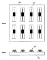
図2は、第1の実施の形態に係るRFIDタグの製造方法を説明するための図である。
図2では、本実施の形態でのRFIDタグの製造工程の一部の様子を、平面図として示してある。本実施の形態では、シート部材11〜13にそれぞれ対応する帯状のシート素材を積層し、それらのシート素材の間に、ICチップ21などの1つのRFIDタグを構成する回路部品を、複数組だけ並列させて配設しておく。そして、これらのシート素材を積層して固着した後に、所定の領域を切り出す。このような工程により、上記のRFIDユニット1が大量に効率よく製造されるようにする。なお、図1は、図2に示した切り出し領域AにおけるX−X矢視から見た断面図に対応している。
FIG. 2 is a diagram for explaining the RFID tag manufacturing method according to the first embodiment.
FIG. 2 is a plan view showing a part of the manufacturing process of the RFID tag in the present embodiment. In the present embodiment, a belt-shaped sheet material corresponding to each of the
RFIDユニット1の製造工程は、ICチップ21が実装された単位ベース基板22をシート部材11に固着する第1の工程と、シート部材11に対して上層シート部材14を積層し、シート部材同士を固着する第2の工程と、積層されたシート部材から1つのRFIDタグの領域を切り出す第3の工程とに大別される。
The manufacturing process of the
第1の工程では、シート部材11に対応する帯状シート素材が、例えばロールに巻き取られた状態で用意される。そして、この帯状シート素材に対して、その長手方向に対して、ICチップ21が実装された単位ベース基板22が並列して固着される。単位ベース基板22が固着された帯状シート素材は、ロールに巻き取っておくことが可能である。
In the first step, a strip-shaped sheet material corresponding to the
第2の工程では、シート部材12,13にそれぞれ対応する帯状シート素材が、例えばロールに巻き取られた状態で用意される。ここで、これらの帯状シート素材の一方には、単位ベース基板22が配設された間隔と同じ間隔で、補強部材23を固着しておく。そして、シート部材11〜13に対応する上記各帯状シート素材をロールから順次引き出して積層し、隣接する帯状シート素材同士を例えば熱圧着などによって固着する。このとき、図2に示すような状態となる。
In the second step, strip-shaped sheet materials respectively corresponding to the
第3の工程では、第2の工程によって帯状シート素材が積層された積層部材から、1つのRFIDタグに対応する切り出し領域Aが、抜き型などによって切り出される。これにより、RFIDユニット1が作製される。
In the third step, the cutout area A corresponding to one RFID tag is cut out by a punching die or the like from the laminated member in which the belt-like sheet materials are laminated in the second step. Thereby, the
以上の製造工程によれば、ICチップ21や導体パターン24などが実装された単位ベース基板22を、シート部材11に対応する帯状シート素材の上にあらかじめ固着しておくとともに、シート部材12,13にそれぞれ対応する帯状シート素材の間にあらかじめ補強部材23を配置しておき、これらの帯状シート部材を上記第2の工程に投入している。
According to the above manufacturing process, the
すなわち、従来はICチップ21および補強部材11の双方を搭載した状態で、保護シートを積層するようにしていたために、ICチップ21および補強部材11の双方の曲げ抵抗により巻き取りができなかったが、これに対して、本実施の形態によれば、シート部材11に対応する帯状シートにICチップ21を実装する一方、シート部材12,13に対応する帯状シートに補強部材23を配置するというように、ICチップ21と補強部材23とを別の帯状シートに配置しておくことができる。その結果、それぞれのシート部材の曲げ抵抗が、ICチップ21および補強部材23の双方を搭載した場合に比べ低くなるので、巻き付けが可能となる。
That is, conventionally, since the protective sheet is laminated in a state where both the
そして、これらのシート部材を積層した段階で、切り出し前のRFIDタグの最終形態を形成することになる。従って、この状態で最終製品の切り出し作業を行えば、ICチップ21および補強部材23の双方を搭載した状態でロールに巻き付けるということがなくなる。
Then, when these sheet members are laminated, the final form of the RFID tag before cutting is formed. Therefore, if the final product is cut out in this state, the
以上により、積層するすべての帯状シート素材をロールに巻き付け、そこから順次引き出して積層するという製造手法が利用可能になる。従って、大量のRFIDユニット1を効率よく製造できる。
As described above, it is possible to use a manufacturing method in which all the belt-like sheet materials to be laminated are wound around a roll and are sequentially drawn out from the rolls and laminated. Therefore, a large number of
なお、単位ベース基板22を作製するための手法としては、例えば、多数の導体パターン24を長手方向に並列して形成した帯状ベース基板を用意し、各導体パターン24に対してICチップ21を実装し、その後に帯状ベース基板から単位ベース基板22の領域を切り離すという手法を適用可能である。
As a method for producing the
また、この手法とは別の手法として、個々の単位ベース基板22を切り離すことなく、多数の単位ベース基板22が長手方向に並列された、シート部材11に対応する帯状シート素材を直接的に作製する手法を採ることも可能である。具体的には、まず、一方の面に粘着材が付着された帯状シート素材を、単位ベース基板22に対応する帯状ベース基板に貼付する。このとき、帯状シート素材は、帯状ベース基板におけるICチップ21の搭載面の反対面に貼付される。次に、この帯状ベース基板において、1つのICチップ21とこれに接続された導体パターン24とを含む領域の周縁部を、粘着剤の層とともに切断する。このとき、シート部材11に対応する帯状シート素材については切断しない。次に、切断した領域の外側領域のみ、帯状ベース基板を帯状シート素材から剥離する。これにより、帯状シート素材には、単位ベース基板22の領域のみが残る。
Further, as a method different from this method, a strip-shaped sheet material corresponding to the
このような手法を用いることで、多数の単位ベース基板22が貼付された帯状シート素材を一旦ロールに巻き取った後、上記の積層工程に投入できるようになり、製造効率をより向上させることができる。
By using such a method, after the strip-shaped sheet material with a large number of
なお、図1および図2の例では、ICチップ21の上方のみに補強部材23を配置したが、さらにICチップ21の下方にも同様な補強部材を配置することも可能である。この場合、シート部材11の下面に、補強部材を挟んでさらにシート部材を積層して固着すればよい。ただし、この場合には、シート部材11またはその下層のシート部材の少なくとも一方を、弾性を有する材料により形成しておく。
In the example of FIGS. 1 and 2, the reinforcing
また、図1および図2の例では、個々のICチップ21ごとに分離された補強部材23が配置されたが、このような補強部材23の代わりに、メッシュ状補強部材が用いられてもよい。この場合、シート部材12,13に対応する帯状シート素材の間に、それらの長手方向に伸びる帯状のメッシュ状補強部材を挟み込んでおく。そして、このような帯状シート素材を上記と同様の手法で積層・固着した後、RFIDユニットに対応する領域を切り出す。このような手法によれば、補強部材を配置する工程の効率をさらに高めることができる。
In the example of FIGS. 1 and 2, the reinforcing
また、後述するように、メッシュ状補強部材を用いた場合には、単位ベース基板22を、シート部材11に対応する帯状シート素材にあらかじめ固着するという工程を省略した手法を用いてもよい。この場合には、導体パターン24を並列して形成した帯状ベース基板に開口部を設けておき、各導体パターン24にICチップ21を接続した後、帯状ベース基板の上下に、メッシュ状補強部材を挟んだ2層の帯状シート素材を含む積層部材をそれぞれ積層し、これらを開口部を介して固着するようにする。
As will be described later, when a mesh-like reinforcing member is used, a method in which the step of fixing the
次に、RFIDタグの製造方法についてのより具体的な実施の形態を説明する。以下の説明では、まず、実施の形態に示されるRFIDタグ製造方法と従来の技術との対比を容易にするために、図3〜図8を用いて一般的なRFIDタグの製造工程の例を挙げる。そして、その後、第2〜第5の実施の形態として、この一般的なRFIDタグの製造工程での問題点を解決した製造工程の具体例について説明する。 Next, a more specific embodiment of the RFID tag manufacturing method will be described. In the following description, first, an example of a general RFID tag manufacturing process will be described with reference to FIGS. 3 to 8 in order to facilitate comparison between the RFID tag manufacturing method shown in the embodiment and the conventional technology. I will give you. Then, specific examples of the manufacturing process that solves the problems in the manufacturing process of the general RFID tag will be described as the second to fifth embodiments.
[一般的なRFIDタグ製造工程]
図3〜図8は、一般的なRFIDタグの製造工程におけるICチップの実装工程を説明するための図である。なお、図3において、上段は、この工程の様子を示す側面図であり、下段は、その平面図である。
[General RFID tag manufacturing process]
3 to 8 are diagrams for explaining an IC chip mounting process in a general RFID tag manufacturing process. In addition, in FIG. 3, the upper stage is a side view which shows the mode of this process, and the lower stage is the top view.
図3において、アンテナ基板101は、多数のアンテナパターン102が一定の間隔で形成されたシート状またはフィルム状の基板である。アンテナパターン102は、例えば、アルミニウムなどの導電材を用いて、印刷技術または薄膜形成技術などによって基板の表面に形成される。図3の例では、それぞれのアンテナパターン102は直線状に形成され、略中央部が離間している。なお、アンテナパターン102の形状としては、他に例えば、ループ状やスパイラル状なども適用可能である。
In FIG. 3, an
非接触型のICチップ103の実装工程では、上記のようにアンテナパターン102が形成されたアンテナ基板101が、ロール121に巻き付けられた状態で用意される。そして、アンテナ基板101は、ロール121を回転させることによってステージ122の上に順次引き出され、このステージ122上において、ICチップ103が順次取り付けられる。
In the mounting process of the non-contact
ICチップ103の取り付けは、例えば、ボンディングツール123を用いたフリップチップボンディングなどによって行われる。ICチップ103の下面または側面には、図示しないアンテナ端子が2つ形成され、これらのアンテナ端子がアンテナパターン102の離間した両側部分のそれぞれに接続される。以上の工程によってICチップ103が実装されたアンテナ基板101は、再度ロールに巻き取られる。
The
図4は、一般的なRFIDタグの製造工程における補強部材の取り付け工程を説明するための図である。
ICチップ103が実装され、ロール131に巻き付けられたアンテナ基板101には、次の工程において、ICチップ103を補強するための補強部材104が取り付けられる。補強部材104の材料としては、例えば、FRP(Fiber-reinforced Plastic)などの樹脂材料、セラミック、金属などが利用可能である。図4の例では、補強部材104は平板状に形成されている。
FIG. 4 is a diagram for explaining a reinforcing member attaching process in a general RFID tag manufacturing process.
In the next step, the reinforcing
ロール131からステージ132上に引き出されたアンテナ基板101上のICチップ103には、まず、ディスペンサ133によって接着剤が塗布される。次に、接着剤が塗布されたICチップ103の上面に、ボンディングツール134によって補強部材104が載置され、さらに熱源135からの熱によって接着剤が硬化される。
First, an adhesive is applied to the
このようにして、ICチップ103の上側に補強部材104が固着されると、アンテナ基板101上にはICチップ103、接着剤および補強部材104による突起が存在する状態となるため、アンテナ基板101をロールで巻き取ることが困難になる。そこで、1個または複数個のICチップ103を単位として、アンテナ基板101をカッター136によって裁断する。そして、裁断された状態のアンテナ基板101を、次の工程のための装置に運搬する。図4の例では、3個のICチップ103が搭載された領域を単位としてアンテナ基板101が裁断されている。
Thus, when the reinforcing
図5は、一般的なRFIDタグの製造工程におけるRFIDインレットの切り出し工程を説明するための図である。なお、図5において、上段は、この工程の様子を示す側面図であり、下段はその平面図である。 FIG. 5 is a diagram for explaining a RFID inlet cutting process in a general RFID tag manufacturing process. In FIG. 5, the upper part is a side view showing the state of this step, and the lower part is a plan view thereof.
前述のように裁断されたアンテナ基板101は、ステージ141の上に載置された後、さらに、抜き型142によって図中の点線に沿って打ち抜かれる。これにより、1つのRFIDタグを構成する電子部品群がパッケージ化されたRFIDインレット105が作製される。
The
図6,図7は、一般的なRFIDタグの製造工程におけるRFIDインレット封止工程について説明するための図である。
まず、図6に示すように、上記の工程により作製された複数のRFIDインレット105が、下側の外装材である下層保護シート106aの上に並べて載置される。下層保護シート106aの材料としては、例えば、PET(Polyethylene Terephthalate)、EPDM(Ethylene Propylene Diene Terpoleymer)、シリコンゴムなどの樹脂材料などが用いられる。なお、図6において、上段は、例として8個のRFIDインレット105が並列された様子を示す平面図であり、下段はその側面図である。
6 and 7 are diagrams for explaining an RFID inlet sealing process in a general RFID tag manufacturing process.
First, as shown in FIG. 6, a plurality of
次に、図7に示すように、テーブル151の上において、RFIDインレット105が載置された下層保護シート106aの上面に、さらに、中間層保護シート106bおよび上層保護シート106cが載置される。なお、中間層保護シート106bは、RFIDインレット105と同等またはそれ以上の厚さを有し、RFIDインレット105に対応する領域がくり抜かれた構成を有している。
Next, as shown in FIG. 7, on the table 151, the intermediate layer
次に、上層保護シート106cの上側から下側方向に対して、プレスヘッド152により加圧されるとともに、加熱される。ここで、下層保護シート106a、中間層保護シート106bおよび上層保護シート106cが、前述の樹脂材料によって形成されている場合には、加圧・加熱により各保護シート同士が固着され、RFIDインレット105が封止される。
Next, the
図8は、一般的なRFIDタグの製造工程における最終製品切り出し工程を説明するための図である。なお、図8において、上段は、この工程の様子を示す側面図であり、下段はその平面図である。 FIG. 8 is a diagram for explaining a final product cutting-out process in a general RFID tag manufacturing process. In addition, in FIG. 8, the upper stage is a side view which shows the mode of this process, and the lower stage is the top view.
図8における保護シート106は、前述の下層保護シート106a、中間層保護シート106bおよび上層保護シート106cが固着された状態の領域を示している。図8に示す工程では、抜き型161によって、個々のRFIDインレット105を包含する領域が打ち抜かれて、最終製品であるRFIDユニット107が作製される。
The
以上の図3〜図8に示した工程により、補強部材104によって補強されたICチップ103やアンテナパターン102などが搭載されたRFIDインレット105の全体を、保護シート106によって封止したRFIDユニット107が製造される。このRFIDユニット107は、曲げや圧迫などの外力に強く、なおかつ、各種の液体や薬剤の中に置かれた場合でもその内部が腐食することなどが防止されるという効果を有する。
The
しかしながら、この一般的な製造方法では、アンテナ基板101上にICチップ103や補強部材104を搭載する工程の後、そのアンテナ基板101をロールで巻き取ることが困難になるため、一旦アンテナ基板101からRFIDインレット105を切り出してから、残りの工程に進む必要がある。ロールを用いた製造手法は、長尺物を容易に持ち運び、そこから長尺物を順次引き出して部品の実装などを連続的に実行できるため、非常に効率がよい製造手法であるが、上記の製造方法では、ロールを用いた製造手法を途中の工程までしか利用できず、製造効率が低いという問題がある。
However, in this general manufacturing method, after the step of mounting the
また、切り出されたRFIDインレット105を封止する工程では、保護シート106の上面を平坦にするために、RFIDインレット105の位置に適合した形状を有する中間層保護シート106bを用いる必要がある。このため、RFIDインレット105の封止工程では、切り出されたRFIDインレット105を所定の位置まで運搬して、正確に位置合わせする必要があり、工程が複雑になってしまう。
Further, in the step of sealing the cut out
本明細書における各実施の形態では、上記のRFIDユニット107とほぼ同様の仕様を持つ製品を、ロールを用いた手法によって一貫して製造することによって、低コストで大量に製造できるようにすることを目的としている。
In each embodiment in this specification, a product having almost the same specifications as the
なお、各実施の形態では、アンテナパターンを直線状のものとするが、アンテナパターンとしては、例えば、ループ状やスパイラル状などのものも適用可能である。
[第2の実施の形態]
図9は、第2の実施の形態に係るRFIDユニットの製造工程の概要を示すフローチャートである。
In each of the embodiments, the antenna pattern is a linear pattern. However, for example, a loop pattern or a spiral pattern can be applied as the antenna pattern.
[Second Embodiment]
FIG. 9 is a flowchart showing an outline of the manufacturing process of the RFID unit according to the second embodiment.
〔ステップS21〕第2の実施の形態では、ICチップの補強部材として、メッシュ状のシート材料を用いる。まず、メッシュ状の補強部材を、弾性を有する保護部材によって挟み込んだ積層シートを作製する。作製された積層シートは、ロールによって巻き取っておく。 [Step S21] In the second embodiment, a mesh sheet material is used as a reinforcing member of the IC chip. First, a laminated sheet is produced in which a mesh-like reinforcing member is sandwiched between protective members having elasticity. The produced laminated sheet is wound up by a roll.
〔ステップS22〕一方、上記の一般的なRFIDタグの製造工程と同様の方法により、アンテナパターンが形成されたアンテナ基板を作製する。作製されたアンテナ基板は、ロールによって巻き取っておく。 [Step S22] On the other hand, an antenna substrate on which an antenna pattern is formed is manufactured by the same method as the above-described general RFID tag manufacturing process. The produced antenna substrate is wound up by a roll.
〔ステップS23〕上記の一般的なRFIDタグの製造工程と同様の方法により、アンテナ基板に対してICチップを実装する。ICチップが実装されたアンテナ基板は、ロールによって巻き取っておくことも可能である。 [Step S23] An IC chip is mounted on the antenna substrate by the same method as the above-described general RFID tag manufacturing process. The antenna substrate on which the IC chip is mounted can be wound up by a roll.
〔ステップS24〕ICチップが実装されたアンテナ基板上の所定の位置に、スリットを形成する。スリットが形成されたアンテナ基板は、ロールによって巻き取っておく。
〔ステップS25〕ステップS24においてスリットが形成されたアンテナ基板を、ステップS21において作製された積層シートによって両側から挟み込み、積層シート同士を固着する。さらに、固着された部材をRFIDタグの領域ごとに切り出し、RFIDユニットを完成させる。この工程では、アンテナ基板と積層シートとを、それぞれのロールから同じ速度で引き出していくことで、積層シート同士を固着し、さらにRFIDユニットを切り出すことができる。
[Step S24] A slit is formed at a predetermined position on the antenna substrate on which the IC chip is mounted. The antenna substrate on which the slit is formed is wound up by a roll.
[Step S25] The antenna substrate on which the slits are formed in Step S24 is sandwiched from both sides by the laminated sheet produced in Step S21, and the laminated sheets are fixed to each other. Further, the fixed member is cut out for each area of the RFID tag to complete the RFID unit. In this step, by pulling out the antenna substrate and the laminated sheet from the respective rolls at the same speed, the laminated sheets can be fixed to each other and the RFID unit can be cut out.
次に、上記各工程について、より詳しく説明する。
図10は、第2の実施の形態における積層シート作製工程を説明するための図である。なお、図10において、上段は、この工程の様子を示す側面図であり、下段はその平面図である。
Next, the above steps will be described in more detail.
FIG. 10 is a diagram for explaining a laminated sheet manufacturing process according to the second embodiment. In addition, in FIG. 10, the upper stage is a side view which shows the mode of this process, and the lower stage is the top view.
図10に示す工程は、図9のステップS21に対応する。この工程では、シート状のナイロンメッシュ201と、ゴムシート202a,202bとが、それぞれロール221,222a,222bに巻き付けられた状態で用意される。そして、これらが積層された積層シートが作製される。
The process shown in FIG. 10 corresponds to step S21 in FIG. In this step, a sheet-
ここで、ナイロンメッシュ201は、非接触型のICチップの補強部材として利用されるものであり、少なくともICチップ全体を包含するだけの幅を有する。この補強部材の材料としては、メッシュ状であればナイロンに限らず、例えば、各種樹脂材料、金網などの金属材料でもよい。ただし、この材料としては、ある程度の剛性を持ち、伸びにくく、かつ、ある程度曲げることができるものが望ましい。また、ICチップの通信性能を良好に保つためには、非導電性であることが望ましい。
Here, the
一方、ゴムシート202a,202bは、後述するように、ICチップ、またはこれが実装された基板に接するシート部材であり、ICチップや基板を保護するために設けられる。この保護シート部材の材料としては、各種の樹脂材料やエラストマなど他の材料でも構わないが、ICチップを押しつけたときにICチップが沈み込む程度の弾性を有することが望ましい。また、後述するように、熱圧着が可能な材料であることがより望ましい。
On the other hand, as will be described later, the
ナイロンメッシュ201、ゴムシート202a,202bは、それぞれロール221,222a,222bから、ローラ223a,223bの間に引き出され、積層される。このとき、ナイロンメッシュ201は、ゴムシート202a,202bによって上下から挟み込まれた状態とされ、ロール224に巻き取られる。
The
なお、この工程においては、ナイロンメッシュ201は、積層されたゴムシート202a,202bに対して、特に接着される必要はない。しかし、例えば、ナイロンメッシュ201の両面、あるいはゴムシート202a,202bのナイロンメッシュ201との対向面に、接着剤を塗布して、その対向面同士を接着するようにしてもよい。
In this step, the
図11は、第2の実施の形態におけるスリット形成工程を説明するための図である。なお、図11において、上段は、この工程の様子を示す側面図であり、下段はその平面図である。 FIG. 11 is a diagram for explaining a slit forming step in the second embodiment. In addition, in FIG. 11, the upper stage is a side view which shows the mode of this process, and the lower stage is the top view.
図9のステップS22で述べたように、積層シートとは別に、アンテナパターンが形成されたアンテナ基板が作製される。次に、図9のステップS23で述べたように、作製されたアンテナ基板に対して、ICチップが実装される。これらの工程に関しては、図3を用いて説明した一般的なRFIDタグの製造工程におけるICチップ実装工程と同様であるので、ここでは図示を省略する。ここで、図11におけるアンテナ基板203、アンテナパターン204およびICチップ205は、図3におけるアンテナ基板101、アンテナパターン102およびICチップ103にそれぞれ対応するものとする。
As described in step S22 of FIG. 9, an antenna substrate on which an antenna pattern is formed is manufactured separately from the laminated sheet. Next, as described in step S23 of FIG. 9, an IC chip is mounted on the manufactured antenna substrate. Since these steps are the same as the IC chip mounting step in the general RFID tag manufacturing step described with reference to FIG. 3, the illustration is omitted here. Here, the
ICチップ205が実装されたアンテナ基板203は、例えば、ロール231に一旦巻き取られた後、図11のスリット形成工程に投入される。ここで、ICチップ205の大きさはアンテナ基板203の幅などに対して小さく、また、その高さは例えば前述の補強部材104に対して低いので、ICチップ205のみを実装したアンテナ基板203は比較的容易にロール231に巻き付けておくことができる。
The
次に、ロール231を回転させて、アンテナ基板203をステージ232上に順次引き出していきながら、抜き型233を用いてアンテナ基板203にスリットを形成していく。図11の例では、並列するアンテナパターン204の間の領域にスリット203aを形成し、アンテナパターン204の長手方向の両端の領域にスリット203bを形成している。
Next, while the
これらのスリットは、後述するシート固着工程において、アンテナ基板203の両側のゴムシート同士を接触させて熱圧着させるために形成される。従って、スリットの大きさや形成場所は、熱圧着時に十分な接着力が生じるように決定される。また、スリットの形成領域は、基本的には、ICチップ205やアンテナパターン204を含まない領域であればどこでも構わない。ただし、後述するように、スリットの形成場所やその大きさによって、完成したRFIDユニットの側面からアンテナ基板203が露出する部分の大きさを小さくすることができる。
These slits are formed so that the rubber sheets on both sides of the
スリットが形成されたアンテナ基板203は、再度ロールに巻き取られる。このロールとしては、アンテナ基板203が巻き付けられていた元のロール231であってもよいし、アンテナ基板203の他端側に設けられた別のロールであってもよい。
The
なお、以上のようなスリットの形成は、ステップS23の工程において、ICチップ205をアンテナ基板203に実装する直前または直後に行われてもよい。あるいは、ステップS21の工程において、アンテナパターン102を形成するために用意するアンテナ基板203に、あらかじめスリットを設けておいてもよい。
The slit formation as described above may be performed immediately before or after mounting the
図12は、第2の実施の形態におけるシート固着・ユニット切り出し工程を説明するための図である。なお、図12において、上段は、この工程の様子を示す側面図であり、下段はその平面図である。 FIG. 12 is a diagram for explaining the sheet adhering / unit cutting-out process in the second embodiment. In FIG. 12, the upper stage is a side view showing the state of this process, and the lower stage is a plan view thereof.
図12に示す工程は、図9のステップS25に対応する。この工程では、まず、ステップS24の工程においてスリットが形成されたアンテナ基板203の両面に、ステップS21の工程においてそれぞれ作製された積層シート206a,206bが積層される。図12において、アンテナ基板203、積層シート206a,206bは、それぞれロール241,242a,242bから引き出され、ローラ243a,243bによって上下方向から加圧されながら搬送される。これとともに、例えば、ローラ243a,243bによって、あるいは、これらとは別の図示しない熱源から、熱が加えられる。
The process shown in FIG. 12 corresponds to step S25 in FIG. In this step, first, the
これにより、積層シート206aの下層側、すなわち、アンテナ基板203に対向する側のゴムシートと、積層シート206bの上層側のゴムシートとが、アンテナ基板203に形成されたスリットを介して熱圧着される。これにより、ICチップ205およびアンテナパターン204が、ゴムシートによって封止される。また、積層シート206aにおいては、上層側のゴムシートと下層側のゴムシートとが、それらの間のナイロンメッシュ201の隙間を介して熱圧着される。同様に、積層シート206bにおいても、上層側のゴムシートと下層側のゴムシートとが、それらの間のナイロンメッシュ201の隙間を介して熱圧着される。
Thus, the rubber sheet on the lower layer side of the
ここで、積層シート206aの下層側のゴムシートは、弾性を有していることから、アンテナ基板203に圧着されたとき、このICチップ205の高さの分だけ収縮する。これにより、積層シート206aの上面はほぼ平坦な状態に保たれる。なお、積層シート206aの上面を平坦にするためには、例えば、ICチップ205の形状に合わせてゴムシートに凹部を設けておいてもよい。ただし、この場合には、アンテナ基板203を挟んだ積層シート206a,206bの固着工程において、積層シート206aの凹部の位置をICチップ205の位置に合わせる必要が生じる。
Here, since the rubber sheet on the lower layer side of the
このように熱圧着されたシート部材は、さらに、抜き型244によって、ICチップ205とこれに接続されたアンテナパターン204とを含む領域ごとに切り出される。ここで切り出されたものが、最終製品であるRFIDユニットとなる。図12の下段では、抜き型244によって切り出される領域を、切り出し領域207として示している。本実施の形態では、切り出し領域207を、アンテナ基板203に形成したスリット203a,203bのそれぞれの内部を通るように設定している。
The sheet member thus thermocompression bonded is further cut out for each region including the
なお、本実施の形態では、ステップS21の工程においてあらかじめ作製した積層シート206a,206bを、ステップS25の工程に投入している。しかし、例えば、ステップS25の工程において、積層シート206a,206bの積層および固着と、これらとアンテナ基板203との積層および固着を、同時に行うようにしてもよい。
In the present embodiment, the
図13は、第2の実施の形態において作製されたRFIDユニットの構成を示す図である。図中の上段はその平面図であり、下段はその側面図である。
図13に示すように、本実施の形態で作製されたRFIDユニットでは、ICチップ205およびアンテナパターン204が、保護部材であるゴムシートによって封止されている。従って、このRFIDユニットに液体や薬剤が付着した場合でも、それらが内部のICチップ205やアンテナパターン204に触れることはなく、ICチップ205を正常に動作させることができる。
FIG. 13 is a diagram illustrating a configuration of an RFID unit manufactured in the second embodiment. The upper stage in the figure is a plan view thereof, and the lower stage is a side view thereof.
As shown in FIG. 13, in the RFID unit manufactured in this embodiment, the
また、ICチップ205の上側および下側には、ナイロンメッシュ201の層が形成されている。このため、このRFIDユニットに外部から圧力が加えられたり、曲げる力が加えられた場合でも、ICチップ205が保護される。なお、ナイロンメッシュ201による補強効果については、後の図14においてさらに説明する。
A layer of
また、ナイロンメッシュ201については、その端面がRFIDユニットの側面から露出している。しかし、ナイロンメッシュ201とICチップ205およびアンテナ基板203との間はゴムシートによって完全に離間しているため、ナイロンメッシュ201が露出していることがICチップ205の動作に与える影響はない。
Further, the end face of the
ただし、このRFIDユニットでは、その側面からアンテナ基板203の端面の一部が露出している。このため、アンテナ基板203の露出部ができるだけ小さくなるように、切り出し前のアンテナ基板203に形成したスリットの位置や大きさと、RFIDユニットを切り出す領域の位置とを決定することが望ましい。
However, in this RFID unit, a part of the end surface of the
本実施の形態では、図12に示したRFIDユニットの切り出し工程では、アンテナ基板203に形成したスリット203a,203bのそれぞれの内部を通るように、切り出し領域207を設定している。これにより、RFIDユニットの側面からアンテナ基板203が露出する部分は、スリット203aと、これに隣接するスリット203bとの間に位置する領域のみとなる。図13ではこの領域を、露出領域208として示している。
In this embodiment, in the RFID unit cut-out process shown in FIG. 12, the cut-out
従って、本実施の形態においては、切り出し前のアンテナ基板203において、並列したアンテナパターン204の間に設けるスリット203aの、アンテナパターン204と平行な方向(図13中の左右方向)の長さを、できるだけ長くすることが望ましい。これに加えて、RFIDユニットのアンテナパターン204と直交する方向(図13上段における上下方向)の長さが、アンテナパターン204の長手方向の両端に設けるスリット203bにおける同方向の長さ以下となるように、スリット203bの大きさおよび切り出し領域207の位置を設定することが望ましい。
Therefore, in the present embodiment, the length of the
なお、例えば、図12において、アンテナ基板203の幅を、積層シート206a,206bの幅より小さくしておき、切り出し領域207の幅方向の長さをアンテナ基板203の幅より大きくするようにしてもよい。この場合、スリット203bを形成せずに、アンテナ基板203のアンテナパターン204の長手方向側の端部が、RFIDユニットの端部から露出しないようになる。
For example, in FIG. 12, the width of the
図14は、ナイロンメッシュによる補強効果を説明するための図である。
図14(A)では、上記のRFIDユニットで用いた保護部材、すなわちゴムシートの断面を示している。このようなシート部材を図中上側が凸部になるように曲げると、一般的に、右側に示すように、シート部材の中心線を基準として、上側には引っ張りの応力が働き、下側には圧縮の応力が働く。
FIG. 14 is a diagram for explaining the reinforcing effect of the nylon mesh.
FIG. 14A shows a cross section of the protective member used in the RFID unit, that is, a rubber sheet. When such a sheet member is bent so that the upper side in the figure becomes a convex portion, generally, as shown on the right side, a tensile stress acts on the upper side with reference to the center line of the sheet member, and the lower side The compression stress works.
本実施の形態で作製されるRFIDユニットでは、ICチップ205の上下にそれぞれナイロンメッシュ201の層が形成されている。ここで、伸びの小さいナイロンメッシュ201を用いた場合、図14(B)に示すように、図中上側が凸部になるようにRFIDユニットを曲げたときには、上側のナイロンメッシュ201の伸び方が小さいために、その領域のゴムシートは曲がりにくい。逆に、図中下側が凸部になるようにRFIDユニットを曲げたときには、下側のナイロンメッシュ201の伸び方が小さいために、同様にゴムシートは曲がりにくい。従って、曲げに対してICチップ205を確実に保護することができる。
In the RFID unit manufactured in this embodiment, layers of
以上の第2の実施の形態では、ICチップの補強部材としてメッシュ状の材料を用い、このメッシュ状補強部材を保護シート部材に積層した積層シートを作製する工程を採り入れた。これにより、RFIDユニットを、ロールを利用して一貫して製造することが可能となる。また、保護シート部材として熱圧着が可能な材料を用いたことにより、上記の積層シートと、ICチップが搭載されたアンテナ基板とを積層し、固着する工程を、効率よく実行可能になる。さらに、保護シート部材として弾性を有する材料を用いたことにより、積層シートとアンテナ基板とを固着する際に、これらの搬送方向に対して特に位置合わせすることなく、積層シートの上面を平坦にすることができる。従って、外力や液体、薬剤などに対して強いRFIDユニットを、低コストで大量に製造することが可能になる。 In the second embodiment described above, a step of producing a laminated sheet in which a mesh-like material is used as a reinforcing member of an IC chip and this mesh-like reinforcing member is laminated on a protective sheet member is employed. As a result, the RFID unit can be manufactured consistently using a roll. Further, by using a material capable of thermocompression bonding as the protective sheet member, it is possible to efficiently execute the process of laminating and adhering the above laminated sheet and the antenna substrate on which the IC chip is mounted. Furthermore, by using a material having elasticity as the protective sheet member, when the laminated sheet and the antenna substrate are fixed, the upper surface of the laminated sheet is flattened without being particularly aligned with the conveying direction. be able to. Accordingly, it is possible to manufacture a large number of RFID units that are strong against external forces, liquids, drugs, and the like at low cost.
[第3の実施の形態]
ところで、上記の第2の実施の形態で作製されるRFIDユニットでは、その側面に補強部材やアンテナ基板の一部が露出する構成となっていた。これに対して、本実施の形態では、補強部材やアンテナ基板が外部に露出しない構成のRFIDユニットを、効率よく製造できるようにする。
[Third Embodiment]
By the way, in the RFID unit manufactured in the second embodiment, a part of the reinforcing member and the antenna substrate is exposed on the side surface. In contrast, in the present embodiment, an RFID unit having a configuration in which the reinforcing member and the antenna substrate are not exposed to the outside can be efficiently manufactured.
図15は、第3の実施の形態に係るRFIDユニットの製造工程の概要を示すフローチャートである。
〔ステップS31〕第3の実施の形態では、上記の一般的なRFIDタグの製造工程と同様の補強部材を利用する。まず、補強部材を、外装となる保護シート部材に実装する。このとき、保護シート部材には、後の工程での位置合わせのためのスプロケットホールを形成しておく。補強部材が実装された保護シート部材は、ロールによって巻き取っておく。
FIG. 15 is a flowchart showing an outline of the manufacturing process of the RFID unit according to the third embodiment.
[Step S31] In the third embodiment, the same reinforcing member as that in the above general RFID tag manufacturing process is used. First, the reinforcing member is mounted on a protective sheet member serving as an exterior. At this time, a sprocket hole for alignment in a later step is formed in the protective sheet member. The protective sheet member on which the reinforcing member is mounted is wound up by a roll.
〔ステップS32〕一方、前述のアンテナ基板上に非接触型のICチップを実装し、ICチップおよびアンテナパターンごとにアンテナ基板を切断することにより、RFIDインレットを作製する。 [Step S32] On the other hand, a non-contact type IC chip is mounted on the above-described antenna substrate, and the RFID substrate is produced by cutting the antenna substrate for each IC chip and antenna pattern.
〔ステップS33〕RFIDインレットを、中間層となるシート部材に実装する。このとき、シート部材には、後の工程での位置合わせのためのスプロケットホールを形成しておく。RFIDインレットが実装されたシート部材は、ロールによって巻き取っておく。 [Step S33] The RFID inlet is mounted on a sheet member serving as an intermediate layer. At this time, a sprocket hole for positioning in a later process is formed in the sheet member. The sheet member on which the RFID inlet is mounted is wound up by a roll.
〔ステップS34〕補強部材が実装された最上層および最下層をなす保護シート部材、RFIDインレットが実装されたシート部材、および、スペーサとしてのシート部材を積層し、シート同士を固着する。さらに、固着された部材をRFIDタグの領域ごとに切り出し、RFIDユニットを完成させる。この工程では、すべてのシート部材をロールから同じ速度で引き出していくことで、シート同士を固着し、さらにRFIDユニットを切り出すことができる。 [Step S34] The protective sheet member forming the uppermost layer and the lowermost layer on which the reinforcing member is mounted, the sheet member on which the RFID inlet is mounted, and the sheet member as a spacer are laminated, and the sheets are fixed to each other. Further, the fixed member is cut out for each area of the RFID tag to complete the RFID unit. In this step, by pulling out all the sheet members from the roll at the same speed, the sheets can be fixed and the RFID unit can be cut out.
次に、上記各工程について、より詳しく説明する。
図16は、補強部材実装・ホール加工工程を説明するための図である。なお、図16において、上段は、この工程の様子を示す側面図であり、下段はその平面図である。
Next, the above steps will be described in more detail.
FIG. 16 is a diagram for explaining a reinforcing member mounting / hole processing step. In FIG. 16, the upper stage is a side view showing the state of this process, and the lower stage is a plan view thereof.
図16に示す工程は、図15のステップS31に対応する。この工程では、保護シート部材であるゴムシート301が、ロール331に巻き付けられた状態で用意される。この保護シート部材は、最終製品であるRFIDユニットの外装を構成する部材であって、内部のICチップやアンテナパターン、補強部材などを封止する機能を果たす。この保護シート部材としては、第1の実施の形態においてナイロンメッシュ201に積層される保護シート部材と同様の材料が用いられればよい。
The process shown in FIG. 16 corresponds to step S31 in FIG. In this step, a
この工程では、ゴムシート301がロール331からステージ332の上に引き出され、実装ツール333によって、ICチップの補強部材302が、ゴムシート301の上面に一定の間隔Pを空けて実装される。補強部材302は、上記の一般的なRFIDタグの製造工程における補強部材104と同様の材料や形状のものが使用されればよい。また、本実施の形態では、補強部材302の下面に、粘着材303が付着される。ここでは例として、粘着材303として両面テープが補強部材302の下面に貼り付けられる。このような補強部材302は、実装ツール333によってゴムシート301上の所定位置に搬送され、ゴムシート301に押しつけられる。なお、粘着材303がゴムシート301上に付着された後、その上に補強部材302が貼付されてもよい。
In this step, the
さらに、この工程では、孔空けツール334により、ゴムシート301上に位置合わせ用のスプロケットホール304が一定間隔で形成される。スプロケットホール304の形成間隔は、例えば、補強部材302が実装される間隔Pと同じであればよい。
Further, in this step, the sprocket holes 304 for alignment are formed at regular intervals on the
以上の工程により補強部材302が実装され、スプロケットホール304が形成されたゴムシート301は、再度ロールに巻き取られる。このロールとしては、ゴムシート301が巻き付けられていた元のロール331であってもよいし、ゴムシート301の他端側に設けられた別のロールであってもよい。
The
図17は、RFIDインレット作製工程を説明するための図である。なお、図17において、上段は、この工程の様子を示す側面図であり、下段はその平面図である。
図17に示す工程は、図15のステップS32に対応する。この工程では、まず、図3を用いて説明した一般的なRFIDタグの製造工程におけるICチップ実装工程と同様の手順により、アンテナ基板311上に非接触型のICチップ312が実装される。すなわち、図17において、アンテナパターン313が形成されたアンテナ基板311が、ロール341からステージ342上に引き出される。そして、例えば、ボンディングツール343を用いたフリップチップボンディングなどにより、ICチップ312がアンテナ基板311に取り付けられ、ICチップ312の端子がアンテナパターン313に接続される。なお、アンテナ基板311、アンテナパターン313の材料や形状などは、上記の一般的なRFIDタグの製造工程の場合と同様でよい。
FIG. 17 is a diagram for explaining the RFID inlet manufacturing process. In FIG. 17, the upper stage is a side view showing the state of this process, and the lower stage is a plan view thereof.
The process shown in FIG. 17 corresponds to step S32 in FIG. In this step, first, the non-contact
次に、ステージ342上では、1組のICチップ312およびアンテナパターン313に対応する領域が、抜き型344によって図中の点線に沿って打ち抜かれる。これにより、1つのRFIDタグを構成する電子部品群がパッケージ化されたRFIDインレットが作製される。
Next, on the
図18は、RFIDインレット実装・ホール加工工程を説明するための図である。なお、図18において、上段は、この工程の様子を示す側面図であり、下段はその平面図である。 FIG. 18 is a diagram for explaining the RFID inlet mounting / hole processing step. In FIG. 18, the upper part is a side view showing the state of this step, and the lower part is a plan view thereof.
図18に示す工程は、図15のステップS33に対応する。この工程では、まず、RFIDユニットの中間層となるシート部材に対して、ステップS32の工程で作製されたRFIDインレットが取り付けられる。本実施の形態では、シート部材としてゴムシート321が用いられる。このシート部材としては、外装となる保護シート部材と同様の材料が用いられればよい。
The process shown in FIG. 18 corresponds to step S33 in FIG. In this process, first, the RFID inlet produced in the process of step S32 is attached to the sheet member serving as the intermediate layer of the RFID unit. In the present embodiment, a
ゴムシート321は、ロール351に巻き付けられた状態で提供される。そして、このゴムシート321がロール351からステージ352の上に引き出され、実装ツール353によって、RFIDインレット322が、ゴムシート321の上面に一定の間隔を空けて実装される。ここで、RFIDインレット322は、ステップS31の工程においてゴムシート301に補強部材302を搭載した際の間隔Pと同じ間隔を空けて、ゴムシート321に搭載される。
The
また、本実施の形態では、RFIDインレット322の下面に、粘着材323が付着される。ここでは例として、ステップS31の工程と同様に、粘着材323として両面テープがRFIDインレット322の下面に貼り付けられる。このようなRFIDインレット322は、実装ツール353によってゴムシート321上の所定位置に搬送され、ゴムシート321に押しつけられて貼付される。なお、粘着材323がゴムシート321上に付着された後、その上にRFIDインレット322が貼付されてもよい。
In this embodiment, the
さらに、この工程では、孔空けツール354により、ゴムシート321上に位置合わせ用のスプロケットホール324が一定間隔で形成される。スプロケットホール324を形成する間隔は、ステップS31の工程においてスプロケットホール304が形成された間隔Pと同じにする必要がある。また、スプロケットホール304の幅方向の間隔についても、ステップS31での形成間隔と同じにする。
Further, in this step, the sprocket holes 324 for alignment are formed at regular intervals on the
以上の工程によりRFIDインレット322が実装され、スプロケットホール324が形成されたゴムシート321は、再度ロールに巻き取られる。このとき、ゴムシート321上に搭載されたRFIDインレット322は比較的薄いものであるため、このようなゴムシート321を比較的容易にロールに巻き付けておくことができる。なお、このロールとしては、ゴムシート321が巻き付けられていた元のロール351であってもよいし、ゴムシート321の他端側に設けられた別のロールであってもよい。
The
図19は、シート固着・ユニット切り出し工程を説明するための図である。なお、図19において、上段は、この工程の様子を示す側面図であり、下段はその平面図である。
図19に示す工程は、図15のステップS34に対応する。この工程では、ステップS33の工程によりRFIDインレット322が実装されたゴムシート321の下層側に、ステップS31の工程により補強部材302が実装されたゴムシート301aが積層される。また、ゴムシート321に上層側には、スペーサシート330を挟んで、ステップS31の工程により補強部材302が実装されたゴムシート301bが積層される。
FIG. 19 is a diagram for explaining the sheet adhering / unit cutting-out process. In FIG. 19, the upper part is a side view showing the state of this step, and the lower part is a plan view thereof.
The process shown in FIG. 19 corresponds to step S34 in FIG. In this step, the
ここで、ゴムシート301a,301bは、搭載された補強部材302が内側を向くようにそれぞれ積層される。また、スペーサシート330は、ゴムシート301a,301b,330と同様の材料により形成されたシート部材である。このスペーサシート330には、ゴムシート301a,301b,321に形成されたものと同じ間隔で、スプロケットホールが形成されているものとする。
Here, the
図19に示すように、ゴムシート301a,301b,321、スペーサシート330は、それぞれロール361a,361b,362,363から引き出され、スプロケットホイール364a,364bの間に搬送される。スプロケットホイール364a,364bには、その外周面上に同じ間隔で凸部が設けられ、これらの凸部がゴムシート301a,301b,321、スペーサシート330にそれぞれ設けられたスプロケットホールに順次挿入されながら搬送される。これにより、ゴムシート321に搭載されたICチップの上下に、ゴムシート301a,301bにそれぞれ搭載された補強部材302が正確に配置されるように位置合わせされる。
As shown in FIG. 19, the
さらに、スプロケットホイール364a,364bの後段にはローラ365a,365bが設けられ、ゴムシート301a,301b,321、スペーサシート330は、ローラ365a,365bによって上下方向から加圧されながら搬送される。このとき、例えば、ローラ365a,365bによって、あるいは、これらとは別の図示しない熱源から、熱が加えられる。これにより、隣接するシート同士が熱圧着され、RFIDインレット322および補強部材302がともに封止される。
Further,
また、積層される各シート、特に、ゴムシート321およびスペーサシート330は、弾性を有していることから、これらのシート部材がローラ365a,365bによって加圧されたとき、シート部材においてRFIDインレット322および補強部材302に接している領域は、RFIDインレット105および補強部材302の高さの分だけ収縮する。これにより、積層されたシート全体の上面はほぼ平坦な状態に保たれる。なお、積層されたシート全体の上面を平坦にするためには、例えば、RFIDインレット322や補強部材302の形状に合わせて、ゴムシート321およびスペーサシート330に凹部を設けておいてもよい。
Further, each sheet to be laminated, in particular, the
このように熱圧着されたシート部材は、さらに、ステージ366上において抜き型367によって、1つのRFIDインレット105を含む領域ごとに切り出される。ここで切り出されたものが、最終製品であるRFIDユニットとなる。図19の下段では、抜き型367によって切り出される領域を、切り出し領域370として示している。この切り出し領域370は、RFIDインレット105とこれに対応する補強部材302の領域より大きく設定され、これにより、RFIDインレット105および補強部材302が上下層のシート部材によって完全に封止される。
The sheet member thus heat-bonded is further cut out for each region including one
なお、本実施の形態では、シート部材積層時の位置合わせのために、各シート部材にスプロケットホールを設けたが、このような孔状のものの他、例えば各シート部材の側部に切り欠きを設けてもよい。この場合、積層工程においては、各シート部材の切り欠きに、スプロケットホイールの凸部に対応する部材を係合させながら各シート部材を搬送すればよい。また、この他の位置合わせ手法が利用されてもよい。 In the present embodiment, each sheet member is provided with sprocket holes for alignment when the sheet members are stacked. In addition to such hole-shaped ones, for example, notches are formed in the side portions of each sheet member. It may be provided. In this case, in the laminating step, each sheet member may be conveyed while engaging the member corresponding to the convex portion of the sprocket wheel in the notch of each sheet member. Other alignment methods may also be used.
また、図19では、ゴムシート301a,301b,321、スペーサシート330のすべてが、一度に積層されている。しかし、これらのうち隣接するシート部材同士をあらかじめ積層し、例えばロールに巻き取った後に、最終的にそれらすべてを積層するという手順が採られてもよい。この場合、シート部材間の固着は、シート部材同士を積層するたびに行われてもよいし、最終的な積層工程で行われてもよい。
In FIG. 19, all of the
図20は、第3の実施の形態において作製されたRFIDユニットの構成を示す図である。図中の上段はその平面図であり、下段はその側面図である。
図20に示すように、本実施の形態で作製されたRFIDユニットでは、RFIDインレット105に搭載されたICチップ312の上層および下層に、それぞれ補強部材302が配置される。ここで、補強部材302としては、前述のように硬質の材料を用いることができるので、第2の実施の形態のように、メッシュ状の材料を用いた場合より、強度を高めることができる。
FIG. 20 is a diagram illustrating a configuration of an RFID unit manufactured in the third embodiment. The upper stage in the figure is a plan view thereof, and the lower stage is a side view thereof.
As shown in FIG. 20, in the RFID unit manufactured in this embodiment, reinforcing
また、ICチップ312、アンテナパターン313およびアンテナ基板311は、すべて保護シート部材の中に封止されており、RFIDユニットの外面に露出していない。このため、このRFIDユニットに液体や薬剤が付着した場合でも、それらが内部のICチップ312やアンテナパターン313に触れることはなく、ICチップ312を正常に動作させることができる。さらに、補強部材302も保護シート部材の中に完全に封止されているので、補強部材302が腐食することも防止される。
Further, the
以上の第3の実施の形態によれば、RFIDユニットを、ロールを利用して一貫して製造することが可能となる。また、保護シート部材として熱圧着が可能な材料を用いたことにより、保護シート部材を積層して固着する工程を、効率よく実行可能になる。さらに、積層する各保護シート部材に位置合わせ用の孔を設けておくことで、保護シート部材を積層して固着する際に、ICチップと補強部材とを簡単に位置合わせすることができる。従って、上記のような特徴を有するRFIDユニットを、低コストで大量に製造することが可能になる。 According to the third embodiment described above, the RFID unit can be manufactured consistently using a roll. Moreover, the process which laminates | stacks and adheres a protective sheet member can be efficiently performed by using the material which can be thermocompression-bonded as a protective sheet member. Furthermore, by providing a hole for alignment in each protective sheet member to be laminated, the IC chip and the reinforcing member can be easily aligned when the protective sheet member is laminated and fixed. Accordingly, a large number of RFID units having the above-described features can be manufactured at low cost.
なお、以上の第3の実施の形態では、ICチップ312の上層および下層の両方に補強部材302を配置したが、例えば、ICチップ312の上層側のみに補強部材302を配置する構成としてもよい。この場合、図19に示したシート固着工程において、下層側のゴムシート301aの積層および固着が省略されればよい。すなわち、この場合には、ゴムシート321がRFIDインレット322を保護する外装の保護シートとして機能する。
In the third embodiment described above, the reinforcing
[第4の実施の形態]
第4の実施の形態は、第2の実施の形態での製造工程の一部を、別の手法によって置き換えたものである。具体的には、ICチップを搭載したアンテナ基板にスリットを入れて、保護シート部材同士を固着する代わりに、ICチップとアンテナ基板とを含むRFIDインレットを中間層の保護シート部材の上に実装することで、保護シート部材同士を固着できるようにする。
[Fourth Embodiment]
In the fourth embodiment, a part of the manufacturing process in the second embodiment is replaced by another method. Specifically, an RFID inlet including the IC chip and the antenna substrate is mounted on the protective sheet member of the intermediate layer instead of slitting the antenna substrate on which the IC chip is mounted and fixing the protective sheet members together. Thus, the protective sheet members can be fixed to each other.
図21は、第4の実施の形態に係るRFIDユニットの製造工程の概要を示すフローチャートである。
〔ステップS41〕この工程では、図9のステップS21の工程と同様の手法で、メッシュ状の補強部材を保護シート部材によって挟み込んだ積層シートを作製する。作製された積層シートは、ロールによって巻き取っておく。
FIG. 21 is a flowchart showing an outline of the manufacturing process of the RFID unit according to the fourth embodiment.
[Step S41] In this step, a laminated sheet is produced in which a mesh-like reinforcing member is sandwiched between protective sheet members in the same manner as in the step S21 of FIG. The produced laminated sheet is wound up by a roll.
〔ステップS42〕上記の積層シートとは別に、ICチップをシート部材に実装する工程が実行される。まず、図9のステップS22,S23の工程と同様の手法で、アンテナパターンが形成されたアンテナ基板を作製し、このアンテナ基板に対してICチップを実装する。 [Step S42] Separately from the above laminated sheet, a process of mounting an IC chip on a sheet member is executed. First, an antenna substrate on which an antenna pattern is formed is produced by the same method as the steps S22 and S23 in FIG. 9, and an IC chip is mounted on the antenna substrate.
〔ステップS43〕ICチップが実装されたアンテナ基板に対して、ベースシート部材を積層する。この工程では、粘着材が付着されたベースシート部材が、アンテナ基板の下面、すなわちICチップが搭載されていない面に固着される。 [Step S43] A base sheet member is laminated on the antenna substrate on which the IC chip is mounted. In this step, the base sheet member to which the adhesive material is attached is fixed to the lower surface of the antenna substrate, that is, the surface on which no IC chip is mounted.
〔ステップS44〕保護シート部材から、ICチップおよびアンテナパターンを含む領域を打ち抜き、RFIDインレットを作製する。この工程では、積層された部材のうちアンテナ基板およびその下層の粘着材の層のみをカットし、RFIDインレットの領域以外のアンテナ基板を剥がして除去する。これにより、RFIDインレットのみが搭載された保護シート部材が作製され、ロールに巻き取られる。 [Step S44] A region including the IC chip and the antenna pattern is punched out of the protective sheet member to produce an RFID inlet. In this step, only the antenna substrate and the underlying adhesive layer are cut from the stacked members, and the antenna substrate other than the RFID inlet region is peeled off and removed. As a result, a protective sheet member on which only the RFID inlet is mounted is produced and wound on a roll.
〔ステップS45〕図9のステップS25の工程と同様の手法で、RFIDインレットが搭載されたベースシート部材を、ステップS41において作製された積層シートによって両側から挟み込み、隣接するシート部材同士を固着する。さらに、固着された部材をRFIDタグの領域ごとに切り出し、RFIDユニットを完成させる。 [Step S45] The base sheet member on which the RFID inlet is mounted is sandwiched from both sides by the laminated sheet prepared in Step S41 by the same method as the step S25 in FIG. 9, and the adjacent sheet members are fixed to each other. Further, the fixed member is cut out for each area of the RFID tag to complete the RFID unit.
次に、上記各工程について、より詳しく説明する。
まず、ステップS41の工程は、図10を用いて説明した通りである。また、ステップS42の工程は、図3を用いて説明した一般的なRFIDタグの製造工程におけるICチップ実装工程と同様である。従って、これらの工程については図示を省略する。
Next, the above steps will be described in more detail.
First, the process of step S41 is as having demonstrated using FIG. The process of step S42 is the same as the IC chip mounting process in the general RFID tag manufacturing process described with reference to FIG. Therefore, illustration of these steps is omitted.
図22は、ベースシート部材積層工程を説明するための図である。
図22に示す工程は、図21のステップS43に対応する。図22において、アンテナ基板401は、ステップS42の工程によりICチップ402が実装され、ロール431に巻き取られた状態でこの工程に投入される。一方、ロール432には、片面に粘着材411が塗布されたゴムシート412が巻き取られている。ゴムシート412は、粘着材411の表面に剥離紙413が貼付された状態でロール432に巻かれている。このゴムシート412は、RFIDインレットを取り付けておくためのベース基材として機能するシート部材であり、ステップS41において用いられる保護シート部材と同様の材料が用いられる。
FIG. 22 is a diagram for explaining the base sheet member stacking step.
The process shown in FIG. 22 corresponds to step S43 in FIG. In FIG. 22, the
図22に示すように、アンテナ基板401およびゴムシート412は、それぞれロール431,432から引き出され、ローラ433a,433bの間に搬送される。このとき、ゴムシート412に貼付されていた剥離紙413は、剥離されてローラ434に巻き取られる。これにより、ゴムシート412の粘着材411の面がアンテナ基板401に接触し、ゴムシート412とアンテナ基板401とが、ローラ433a,433bの圧力によって圧着される。圧着されたゴムシート412およびアンテナ基板401は、ステージ435に搬送されて、ローラに巻き取られることなく、次の工程に投入される。
As shown in FIG. 22, the
なお、アンテナ基板401に接触するローラ433aについては、ICチップ402を圧力により破損しない程度に柔らかい材料により形成されていることが望ましい。
図23は、RFIDインレット打ち抜き工程を説明するための図である。なお、図23において、上段は、この工程の様子を示す側面図であり、下段はその平面図である。
Note that the
FIG. 23 is a diagram for explaining the RFID inlet punching process. In FIG. 23, the upper stage is a side view showing the state of this process, and the lower stage is a plan view thereof.
図23に示す工程は、図21のステップS44に対応する。上記工程により圧着されたゴムシート412およびアンテナ基板401は、ステージ435での打ち抜き工程に投入される。この工程では、抜き型436によって、アンテナ基板401と、ゴムシート401における粘着材411の層のみがカットされ、ゴムシート412はカットされない。
The process shown in FIG. 23 corresponds to step S44 in FIG. The
この後、ローラ437の位置において、アンテナ基板401のうち抜き型436によりカットされた領域の外側の部分が、ゴムシート412から剥離されて、例えばロール438に巻き取られる。一方、ゴムシート412は、ロール439によって巻き取られる。
Thereafter, at the position of the
ここで、抜き型436によってカットされる領域については、下段の図において点線で示してある。この図に示すように、1組のICチップ402およびアンテナパターン403に対応する領域が、抜き型436によってカットされる。従って、カットされた領域の外側のみがゴムシート412から剥離されると、ロール439に巻き取られるゴムシート412は、ICチップ402およびアンテナパターン403を含む領域のみが貼付された状態となる。すなわち、このゴムシート412の上に、1つのRFIDタグを構成する電子部品群がパッケージ化されたRFIDインレット404が作製される。
Here, the region cut by the punching die 436 is indicated by a dotted line in the lower diagram. As shown in this figure, a region corresponding to one set of
なお、このとき作製される、RFIDインレット404が貼付されたゴムシート412は、第3の実施の形態におけるRFIDインレット実装工程(図15のステップS33)において作製されるものと、ほぼ同じ構成を有するものとなる。ただし、本実施の形態では、スプロケットホールは形成されない。
The
図24は、シート固着・ユニット切り出し工程を説明するための図である。なお、図24において、上段は、この工程の様子を示す側面図であり、下段はその平面図である。
図24に示す工程は、図21のステップS45に対応する。この工程の基本的な手順は、第2の実施の形態において、図10のステップS25に示したシート固着・ユニット切り出し工程とほぼ同様である。また、この工程については、図12を用いてすでに説明した。このため、図24では、図12と同じ構成要素には同じ符号を付して示している。
FIG. 24 is a diagram for explaining the sheet adhering / unit cutting-out step. In FIG. 24, the upper part is a side view showing the state of this step, and the lower part is a plan view thereof.
The process shown in FIG. 24 corresponds to step S45 in FIG. The basic procedure of this process is substantially the same as the sheet adhering / unit cutting process shown in step S25 of FIG. 10 in the second embodiment. This process has already been described with reference to FIG. For this reason, in FIG. 24, the same components as those in FIG.
図24に示す工程は、図12に示したアンテナ基板203の代わりに、図21のステップS42〜S44の工程によって作製された、RFIDインレット404付きのゴムシート412を用いたものである。すなわち、ゴムシート412、積層シート206a,206bは、それぞれロール439,242a,242bから引き出され、ローラ243a,243bによって上下方向から加圧されながら搬送される。これとともに、例えば、ローラ243a,243bによって、あるいは、これらとは別の図示しない熱源から、熱が加えられる。
The process shown in FIG. 24 uses a
これにより、積層シート206aの下層側のゴムシートと、ゴムシート412の上面とが熱圧着される。これにより、ICチップ402およびアンテナパターン403が、ゴムシートによって封止される。また、積層シート206bの上層側のゴムシートと、ゴムシート412の下面との間も熱圧着される。そして、第2の実施の形態と同様、各積層シート206a,206b内の2枚のゴムシート同士も熱圧着される。
Thereby, the rubber sheet on the lower layer side of the
また、これらすべてのシート部材が圧着されると、積層シート206aがRFIDインレット404の高さに応じて収縮するため、積層シート206aの上面はほぼ平坦な状態に保たれる。なお、積層シート206aの上面を平坦にするためには、例えば、RFIDインレット404の形状に合わせてゴムシートに凹部を設けておいてもよい。ただし、この場合には、ゴムシート412を挟んだ積層シート206a,206bの固着工程において、積層シート206aの凹部の位置をRFIDインレット404の位置に合わせる必要が生じる。
When all these sheet members are pressure-bonded, the
このように熱圧着されたシート部材は、さらに、抜き型244によって、RFIDインレット404を含む領域ごとに切り出される。ここで切り出されたものが、最終製品であるRFIDユニットとなる。図24の下段では、抜き型244によって切り出される領域を、切り出し領域405として示している。
The sheet member thus thermocompression bonded is further cut out for each region including the
なお、本実施の形態では、ステップS41の工程においてあらかじめ作製した積層シート206a,206bを、ステップS45の工程に投入している。しかし、例えば、ステップS45の工程において、積層シート206a,206bの積層および固着と、これらとゴムシート412との積層および固着を、同時に行うようにしてもよい。
In the present embodiment, the
また、図24に示した工程においては、積層シート206a,206bのうち、ゴムシート412の下面に固着する積層シート206bについては、ゴムシート412側の面のゴムシートが省略され、ナイロンメッシュが直接ゴムシート412に接触するようにしてもよい。ただし、図24のような工程とすることで、ゴムシート412の両面側に対して全く同じ製造工程によって製造された積層シート206a,206bを利用可能になり、製造工程が簡略化されるというメリットが生じる。
In the process shown in FIG. 24, the
図25は、第4の実施の形態において作製されたRFIDユニットの構成を示す図である。図中の上段はその平面図であり、下段はその側面図である。
図25に示すように、本実施の形態で作製されたRFIDユニットでは、第2の実施の形態の場合と同様に、ICチップ402の上側および下側に、ナイロンメッシュ201の層が形成される。これにより、外力からICチップ402が保護される。なお、第2の実施の形態と同様に、ナイロンメッシュ201の端面は、RFIDユニットの側面に露出した状態となる。
FIG. 25 is a diagram showing a configuration of an RFID unit manufactured in the fourth embodiment. The upper stage in the figure is a plan view thereof, and the lower stage is a side view thereof.
As shown in FIG. 25, in the RFID unit manufactured in the present embodiment, a layer of
また、このRFIDユニットにおいては、ICチップ402およびアンテナパターン403を備えたRFIDインレット404が、保護部材であるゴムシートによって完全に封止されている。すなわち、第2の実施の形態の場合と異なり、RFIDインレット404に含まれるアンテナ基板401全体が、ゴムシートによって封止される。このため、液体や薬剤が付着した場合でも、ICチップ205をより強固に保護することができる。
In this RFID unit, the
以上の第4の実施の形態によれば、粘着材付きのゴムシートをRFIDインレットのベースシート部材として使用することで、ロールに巻き取り可能なシート部材からRFIDインレットを一旦切り離す必要がなくなる。このため、RFIDユニットの製造工程において、一貫してロールを利用した製造手法を採ることが可能になる。しかも、RFIDインレットが保護シート部材によって完全に封止された構造のRFIDユニットを製造できる。従って、外力や液体、薬剤などに対して強いRFIDユニットを、低コストで大量に製造することが可能になる。 According to the fourth embodiment described above, by using a rubber sheet with an adhesive as a base sheet member of an RFID inlet, it is not necessary to once separate the RFID inlet from a sheet member that can be wound around a roll. For this reason, in the manufacturing process of the RFID unit, it is possible to consistently adopt a manufacturing method using a roll. Moreover, an RFID unit having a structure in which the RFID inlet is completely sealed by the protective sheet member can be manufactured. Accordingly, it is possible to manufacture a large number of RFID units that are strong against external forces, liquids, drugs, and the like at low cost.
なお、以上の第4の実施の形態では、ICチップ402の上層および下層の両方に補強用のナイロンメッシュ201を配置したが、例えば、ICチップ402の上層側のみにナイロンメッシュ201を配置してもよい。この場合、図24に示したシート固着工程では、下層側の積層シート206bの積層および固着が省略される。ただし、図14で説明したように、曲げに対する強度を確保するためには、ナイロンメッシュ201をICチップ402の上層および下層の両方に配置しておくことが望ましい。
In the fourth embodiment described above, the reinforcing
[第5の実施の形態]
第5の実施の形態では、第3の実施の形態における製造工程の一部を、第4の実施の形態におけるRFIDインレットの製造工程によって置き換える。
[Fifth Embodiment]
In the fifth embodiment, a part of the manufacturing process in the third embodiment is replaced by the RFID inlet manufacturing process in the fourth embodiment.
図26は、第5の実施の形態に係るRFIDユニットの製造工程の概要を示すフローチャートである。
〔ステップS51〕この工程では、図15のステップS31の工程と同様の手法で、硬質な補強部材を保護シート部材に実装し、さらに、位置合わせ用のスプロケットホールを形成する。補強部材が実装された保護シート部材は、ロールによって巻き取っておく。
FIG. 26 is a flowchart showing an outline of the manufacturing process of the RFID unit according to the fifth embodiment.
[Step S51] In this step, a hard reinforcing member is mounted on the protective sheet member in the same manner as in the step S31 in FIG. 15, and a sprocket hole for alignment is formed. The protective sheet member on which the reinforcing member is mounted is wound up by a roll.
〔ステップS52〜S54〕これらの工程では、図21のステップS42〜S44と同様の手法で、RFIDインレット付きの保護シート部材を作製する。ただし、ステップS54の工程において、保護シート部材にスプロケットホールを形成する工程が加わっている点のみが異なる。 [Steps S52 to S54] In these steps, a protective sheet member with an RFID inlet is manufactured in the same manner as steps S42 to S44 of FIG. However, the only difference is that the step of forming a sprocket hole in the protective sheet member is added to the step S54.
〔ステップS55〕図15のステップS34の工程と同様の手法で、RFIDインレット付きの保護シート部材と、補強部材が実装された最上層および最下層をなす保護シート部材と、スペーサとしてのシート部材とを積層し、シート同士を固着する。さらに、固着された部材をRFIDタグの領域ごとに切り出し、RFIDユニットを完成させる。 [Step S55] In the same manner as in step S34 in FIG. 15, a protective sheet member with an RFID inlet, a protective sheet member having the uppermost layer and the lowermost layer on which a reinforcing member is mounted, a sheet member as a spacer, Are laminated and the sheets are fixed to each other. Further, the fixed member is cut out for each area of the RFID tag to complete the RFID unit.
次に、上記各工程について、より詳しく説明する。
まず、ステップS51の工程は、図16を用いて説明した通りである。また、ステップS52の工程は、図3を用いて説明した一般的なRFIDタグの製造工程におけるICチップ実装工程と同様である。さらに、ステップS53の工程は、図22を用いて説明した通りである。従って、これらの工程については図示を省略する。
Next, the above steps will be described in more detail.
First, the step S51 is as described with reference to FIG. Further, the process of step S52 is the same as the IC chip mounting process in the general RFID tag manufacturing process described with reference to FIG. Further, the step S53 is as described with reference to FIG. Therefore, illustration of these steps is omitted.
図27は、ホール加工・RFIDインレット打ち抜き工程を説明するための図である。なお、図27において、上段は、この工程の様子を示す側面図であり、下段はその平面図である。 FIG. 27 is a diagram for explaining the hole processing / RFID inlet punching process. In FIG. 27, the upper part is a side view showing the state of this step, and the lower part is a plan view thereof.
図27に示す工程は、図26のステップS54に対応する。この工程の基本的な手順は、第4の実施の形態において、図21のステップS44に示したRFIDインレット打ち抜き工程とほぼ同様である。また、この工程については、図23を用いてすでに説明した。このため、図27では、図23と同じ構成要素については同じ符号を付して示している。ただし、図27中のアンテナ基板401a、ゴムシート412aおよびロール439aは、それぞれ図23中のアンテナ基板401、ゴムシート412およびロール439に対応している。
The process shown in FIG. 27 corresponds to step S54 in FIG. The basic procedure of this process is almost the same as the RFID inlet punching process shown in step S44 of FIG. 21 in the fourth embodiment. This process has already been described with reference to FIG. Therefore, in FIG. 27, the same components as those in FIG. 23 are denoted by the same reference numerals. However, the
図27に示す工程は、図23で説明した工程に対して、さらに、スプロケットホール501を形成する工程を加えたものである。スプロケットホール501は、孔空けツール511により、アンテナ基板401aおよびゴムシート412aに対して一定間隔で形成される。ここで、スプロケットホール501を形成する間隔は、ステップS51におけるスプロケットホールの形成間隔と同じにされる。なお、スプロケットホール501の形成工程は、抜き型436によるアンテナ基板401aのカット工程の前に限定されず、その後に行われてもよい。例えば、アンテナ基板401aの余計な領域がゴムシート412aから剥離された後に、このゴムシート412aに対してスプロケットホール501が形成されてもよい。
The process shown in FIG. 27 is obtained by adding a process of forming
このような工程により、ロール439aに巻き取られるゴムシート412aは、ICチップ402およびアンテナパターン403を含む領域のみが貼付された状態となる。すなわち、このゴムシート412aの上に、1つのRFIDタグを構成する電子部品群がパッケージ化されたRFIDインレット404が作製される。なお、このとき作製される、RFIDインレット404が貼付されたゴムシート412aは、第3の実施の形態におけるRFIDインレット実装工程(図15のステップS33)において作製されるものと同じ構成を有するものとなる。
By such a process, the
図28は、シート固着・ユニット切り出し工程を説明するための図である。なお、図28において、上段は、この工程の様子を示す側面図であり、下段はその平面図である。
図28に示す工程は、図26のステップS55に対応する。この工程の基本的な手順は、第3の実施の形態において、図15のステップS34に示したシート固着・ユニット切り出し工程と同じである。また、この工程については、図19を用いてすでに説明した。このため、図28では、図19と同じ構成要素については同じ符号を付して示している。
FIG. 28 is a diagram for explaining the sheet adhering / unit cutting-out step. In FIG. 28, the upper stage is a side view showing the state of this process, and the lower stage is a plan view thereof.
The process shown in FIG. 28 corresponds to step S55 in FIG. The basic procedure of this process is the same as the sheet adhering / unit cutting process shown in step S34 of FIG. 15 in the third embodiment. This process has already been described with reference to FIG. For this reason, in FIG. 28, the same components as those in FIG. 19 are denoted by the same reference numerals.
図28に示す工程では、図19に示した、RFIDインレット322付きのゴムシート321の代わりに、図26のステップS54の工程により作製された、RFIDインレット404付きのゴムシート412aが用いられる。このゴムシート412aは、ロール439から引き出されて、スプロケットホイール364a,364bによって搬送される。そして、下層、上層の各ゴムシート301a,301bおよびスペーサシート330と積層され、熱圧着される。
In the process shown in FIG. 28, the
これらすべてのシート部材が圧着されると、スペーサシート330がRFIDインレット404の高さに応じて収縮するため、積層されたシート全体の上面はほぼ平坦な状態に保たれる。なお、シート全体の上面を平坦にするためには、例えば、RFIDインレット404の形状に合わせてスペーサシート330に凹部を設けておいてもよい。
When all these sheet members are pressure-bonded, the
このように熱圧着されたシート部材は、さらに、ステージ366上において抜き型367によって、1つのRFIDインレット404を含む領域ごとに切り出される。ここで切り出されたものが、最終製品であるRFIDユニットとなる。図28の下段では、抜き型367によって切り出される領域を、切り出し領域370として示している。この切り出し領域370は、RFIDインレット404とこれに対応する補強部材302の領域より大きく設定され、これにより、RFIDインレット404および補強部材302が上下層のシート部材によって完全に封止される。
The sheet member thus thermocompression bonded is further cut out for each region including one
なお、本実施の形態では、シート部材積層時の位置合わせのために、各シート部材にスプロケットホールを設けたが、上記の第3の実施の形態と同様、このような孔状のものの他、例えば各シート部材の側部に切り欠きを設けてもよい。また、この他の位置合わせ手法が利用されてもよい。 In the present embodiment, each sheet member is provided with a sprocket hole for alignment at the time of sheet member lamination, but in the same manner as in the third embodiment, For example, you may provide a notch in the side part of each sheet | seat member. Other alignment methods may also be used.
また、図28では、ゴムシート301a,301b,412a、スペーサシート330のすべてが、一度に積層されている。しかし、これらのうち隣接するシート部材同士をあらかじめ積層し、例えばロールに巻き取った後に、最終的にそれらすべてを積層するという手順が採られてもよい。この場合、シート部材間の固着は、シート部材同士を積層するたびに行われてもよいし、最終的な積層工程で行われてもよい。
In FIG. 28, all of the
図29は、第5の実施の形態において作製されたRFIDユニットの構成を示す図である。図中の上段はその平面図であり、下段はその側面図である。なお、図29では、図20と同じ構成要素については同じ符号を付して示している。 FIG. 29 is a diagram showing a configuration of an RFID unit manufactured in the fifth embodiment. The upper stage in the figure is a plan view thereof, and the lower stage is a side view thereof. In FIG. 29, the same components as those in FIG. 20 are denoted by the same reference numerals.
図29に示すように、本実施の形態で作製されたRFIDユニットは、図20に示した、第3の実施の形態において作製されたRFIDユニットとほぼ同じ構成を有している。すなわち、RFIDインレット404に搭載されたICチップ402の上層および下層に、それぞれ補強部材302が配置される。また、ICチップ402、アンテナパターン403、アンテナ基板401および補強部材302は、すべて保護シート部材の中に封止されており、RFIDユニットの外面に露出していない。
As shown in FIG. 29, the RFID unit manufactured in the present embodiment has almost the same configuration as the RFID unit manufactured in the third embodiment shown in FIG. That is, the reinforcing
以上の第5の実施の形態によれば、第3の実施の形態において作製されるものと同様の特徴を有するRFIDユニットを、より効率よく製造することが可能である。すなわち、第5の実施の形態では、粘着材付きのゴムシートをRFIDインレットのベースシート部材として使用することで、ロールに巻き取り可能なシート部材からRFIDインレットを一旦切り離す必要がなくなる。このため、RFIDユニットの製造工程において、一貫してロールを利用した製造手法を採ることが可能になる。 According to the above fifth embodiment, it is possible to more efficiently manufacture an RFID unit having the same characteristics as those manufactured in the third embodiment. That is, in the fifth embodiment, by using a rubber sheet with an adhesive as a base sheet member of an RFID inlet, it is not necessary to once separate the RFID inlet from a sheet member that can be wound around a roll. For this reason, in the manufacturing process of the RFID unit, it is possible to consistently adopt a manufacturing method using a roll.
なお、以上の第5の実施の形態では、ICチップの上層および下層の両方に補強部材302を配置したが、前述した第3の実施の形態と同様に、例えば、ICチップの上層側のみに補強部材302を配置する構成としてもよい。この場合、図28に示したシート固着工程において、下層側のゴムシート301aの積層および固着が省略されればよい。
In the fifth embodiment described above, the reinforcing
また、上記の第2〜第5の実施の形態において、図6のステップS25、図15のステップS34、図21のステップS45、図26のステップS55のそれぞれでのシート固着工程では、熱圧着の代わりに、例えば、超音波を用いてシート部材同士を固着してもよい。あるいは、接着剤を用いてシート部材同士が固着されてもよい。ただし、接着剤を用いた場合には、例えば、アンテナ基板やシート部材などの必要な面に接着剤を塗布する工程が必要になる。これに対して、上記各実施の形態のように、接着剤を用いない手法により複数のシート部材を一度に固着することで、製造効率を高めることができる。また、接着剤を用いず、シート部材同士を直接固着させる手法を用いることで、各層のシート部材が剥がれにくくなるので、その内部をより確実に封止することができる。さらに、いずれの固着手法を用いた場合でも、シート部材同士を加圧して、積層されたシート部材の表面が平坦になるようにすることが望ましい。 In the second to fifth embodiments described above, in the sheet adhering process in step S25 of FIG. 6, step S34 of FIG. 15, step S45 of FIG. 21, and step S55 of FIG. Instead, for example, the sheet members may be fixed using ultrasonic waves. Alternatively, the sheet members may be fixed using an adhesive. However, when an adhesive is used, for example, a process of applying the adhesive to a necessary surface such as an antenna substrate or a sheet member is required. On the other hand, the manufacturing efficiency can be increased by fixing a plurality of sheet members at a time using a technique that does not use an adhesive, as in the above embodiments. Moreover, since the sheet member of each layer becomes difficult to peel by using the method of directly adhering sheet members without using an adhesive, the inside can be more reliably sealed. Furthermore, in any case, it is desirable to pressurize the sheet members so that the surface of the laminated sheet members becomes flat.
以上の実施の形態に関し、さらに以下の付記を開示する。
(付記1) アンテナとして機能する導体パターンが形成されているとともに、前記導体パターンに接続した非接触通信型の回路チップが実装された単位ベース基板と、帯状の第1のシート部材とを備え、前記第1のシート部材上にその長手方向に沿って前記単位ベース基板が一定の間隔で固着されたベースシート部材を形成するベースシート部材形成工程と、
それぞれ帯状であって弾性を有する第2のシート部材と第3のシート部材との間に、前記回路チップを補強するための補強部材を前記回路チップの配置間隔と同じ間隔で配置した状態で積層することにより、上層シート部材を形成するとともに、前記上層シート部材を、前記ベースシート部材形成工程により形成された前記ベースシート部材における前記単位ベース基板の積層面側に対して、前記回路チップと前記補強部材とがシート平面側から見て重なる状態で積層するシート部材積層工程と、
前記シート部材積層工程により積層されたシートから、1つの前記単位ベース基板を内包する領域を順次切り出す切り出し工程と、
を有することを特徴とするRFIDタグの製造方法。
Regarding the above embodiment, the following additional notes are disclosed.
(Supplementary note 1) A conductor pattern that functions as an antenna is formed, and a unit base substrate on which a non-contact communication type circuit chip connected to the conductor pattern is mounted, and a strip-shaped first sheet member, A base sheet member forming step of forming a base sheet member in which the unit base substrate is fixed at a predetermined interval along the longitudinal direction on the first sheet member;
A reinforcing member for reinforcing the circuit chip is laminated between the second sheet member and the third sheet member, each of which has a belt shape and elasticity, in a state where the reinforcing members are arranged at the same intervals as the circuit chips. The upper layer sheet member is formed, and the circuit chip and the upper layer sheet member are arranged on the side of the unit base substrate on the base sheet member formed by the base sheet member forming step. A sheet member laminating step of laminating the reinforcing member and the reinforcing member when viewed from the sheet plane side;
A cutout step of sequentially cutting out a region containing one unit base substrate from the sheets laminated by the sheet member lamination step;
The manufacturing method of the RFID tag characterized by having.
(付記2) 前記導体パターンが長手方向に前記一定の間隔で形成された帯状のベース基板に対して、前記回路チップを順次実装して対応する前記導体パターンに接続させる回路チップ実装工程をさらに有し、
前記ベースシート部材形成工程は、
一方の面に粘着材が付着された前記第1のシート部材を、前記ベース基板の前記回路チップの実装面とは反対の面に前記粘着材を介して貼付する工程と、
前記ベース基板が貼付された前記第1のシート部材において、1つの前記回路チップとこれに接続された前記導体パターンとを囲む領域の周縁部を、前記ベース基板および前記粘着材の各層のみ切断する工程と、
前記第1のシート部材から、前記ベース基板のうち前記周縁部の外側領域のみを剥離して、前記単位ベース基板が固着された前記ベースシート部材を形成する工程と、
を有することを特徴とする付記1記載のRFIDタグの製造方法。
(Supplementary Note 2) A circuit chip mounting step is further provided in which the circuit chips are sequentially mounted and connected to the corresponding conductor patterns on the strip-shaped base substrate in which the conductor patterns are formed at the predetermined intervals in the longitudinal direction. And
The base sheet member forming step includes
A step of attaching the first sheet member with the adhesive material attached to one surface to the surface of the base substrate opposite to the mounting surface of the circuit chip via the adhesive material;
In the first sheet member to which the base substrate is affixed, only the base substrate and each layer of the adhesive material are cut at a peripheral portion of a region surrounding one circuit chip and the conductor pattern connected thereto. Process,
Peeling only the outer region of the peripheral portion of the base substrate from the first sheet member to form the base sheet member to which the unit base substrate is fixed; and
The manufacturing method of the RFID tag according to
(付記3) 前記シート部材積層工程では、前記ベースシート部材側の面に前記回路チップごとに分離された前記補強部材が前記回路チップの配置間隔と同じ間隔で固着された前記第3のシート部材を、前記第2のシート部材を挟んで前記ベースシート部材に積層し、
前記切り出し工程では、前記上層シート部材と前記ベースシート部材とが積層されたシートから、1つの前記単位ベース基板と当該単位ベース基板上の前記回路チップに対応する前記補強部材とを内包する領域を順次切り出す、
ことを特徴とする付記1または2に記載のRFIDタグの製造方法。
(Additional remark 3) In the said sheet member lamination process, the said 3rd sheet member by which the said reinforcement member isolate | separated for every said circuit chip was fixed to the surface at the side of the said base sheet member at the same space | interval as the arrangement | positioning space | interval of the said circuit chip. Are stacked on the base sheet member with the second sheet member interposed therebetween,
In the cutting-out step, an area including one unit base substrate and the reinforcing member corresponding to the circuit chip on the unit base substrate from a sheet in which the upper layer sheet member and the base sheet member are laminated is provided. Cut out sequentially,
The manufacturing method of the RFID tag according to
(付記4) 前記シート部材積層工程では、前記第1のシート部材と前記第2のシート部材、および、前記第2のシート部材と前記第3のシート部材を、それぞれ熱圧着することを特徴とする付記3記載のRFIDタグの製造方法。 (Appendix 4) In the sheet member lamination step, the first sheet member and the second sheet member, and the second sheet member and the third sheet member are thermocompression bonded, respectively. The manufacturing method of the RFID tag as described in appendix 3.
(付記5) 前記シート部材積層工程では、前記第1のシート部材、前記第2のシート部材および前記第3のシート部材にそれぞれ同一間隔で形成された孔または切り欠きの位置を合わせながら、前記第1のシート部材、前記第2のシート部材および前記第3のシート部材を搬送して積層することで、前記回路チップと対応する前記補強部材との位置を合わせることを特徴とする付記3または4に記載のRFIDタグの製造方法。 (Additional remark 5) In the said sheet member lamination process, adjusting the position of the hole or notch respectively formed in the said 1st sheet member, the said 2nd sheet member, and the said 3rd sheet member at the same space | interval, Supplementary note 3 or 3, wherein the first chip member, the second sheet member, and the third sheet member are conveyed and stacked to align the circuit chip and the corresponding reinforcing member. 4. A manufacturing method of the RFID tag according to 4.
(付記6) 前記第1のシート部材は弾性を有する材料により形成され、
前記シート部材積層工程では、前記回路チップごとに分離された下層側補強部材が前記回路チップの配置間隔と同じ間隔で固着された、弾性を有する第4のシート部材を、前記回路チップと前記下層側補強部材とがシート平面側から見て重なる状態で、前記第1のシート部材における前記単位ベース基板の固着面の反対面にさらに積層する、
ことを特徴とする付記3〜5のいずれか1つに記載のRFIDタグの製造方法。
(Appendix 6) The first sheet member is formed of an elastic material,
In the sheet member laminating step, a fourth sheet member having elasticity, in which lower layer side reinforcing members separated for each circuit chip are fixed at the same interval as the arrangement interval of the circuit chips, is used as the circuit chip and the lower layer. In a state where the side reinforcing member overlaps with the sheet plane side, it is further laminated on the surface opposite to the fixing surface of the unit base substrate in the first sheet member.
The method for manufacturing an RFID tag according to any one of Supplementary notes 3 to 5, wherein:
(付記7) 前記シート部材積層工程では、前記補強部材として、少なくとも前記回路チップを包含する幅を有し、前記第2のシート部材および前記第3のシート部材の長手方向に帯状に長く形成されたメッシュ状補強部材を、前記第2のシート部材と前記第3のシート部材との間に挟んで配置することを特徴とする付記1または2に記載のRFIDタグの製造方法。
(Additional remark 7) In the said sheet member lamination process, it has a width | variety which includes at least the said circuit chip as said reinforcement member, and is formed long in the strip | belt shape in the longitudinal direction of a said 2nd sheet member and a said 3rd sheet member. 3. The RFID tag manufacturing method according to
(付記8) 前記シート部材積層工程では、前記メッシュ状補強部材と同様の下層側メッシュ状補強部材を、弾性を有する第4のシート部材と第5のシート部材との間に挟んだ下層シート部材を、当該下層側メッシュ状補強部材と前記回路チップとがシート平面側から見て重なる状態で、前記第1のシート部材における前記単位ベース基板の固着面に対する反対面にさらに積層することを特徴とする付記7記載のRFIDタグの製造方法。 (Additional remark 8) In the said sheet member lamination process, the lower layer sheet member which pinched | interposed the lower layer side mesh-shaped reinforcement member similar to the said mesh-shaped reinforcement member between the 4th sheet member and 5th sheet member which have elasticity Is further laminated on the surface of the first sheet member opposite to the fixing surface of the unit base substrate in a state where the lower layer mesh reinforcing member and the circuit chip overlap when viewed from the sheet plane side. The manufacturing method of the RFID tag as described in appendix 7.
(付記9) 前記シート部材積層工程では、前記第1のシート部材と前記第2のシート部材、および、前記第2のシート部材と前記第3のシート部材を、それぞれ熱圧着することを特徴とする付記7記載のRFIDタグの製造方法。 (Supplementary Note 9) In the sheet member stacking step, the first sheet member and the second sheet member, and the second sheet member and the third sheet member are respectively thermocompression bonded. The manufacturing method of the RFID tag as described in appendix 7.
(付記10) 前記第2のシート部材と前記第3のシート部材との間に前記メッシュ状補強部材を挟んでロールに巻き取ることにより、前記上層シート部材を作製する上層シート部材作製工程をさらに有し、
前記シート部材積層工程では、前記上層シート部材がロールから引き出されて投入されることを特徴とする付記8または9に記載のRFIDタグの製造方法。
(Additional remark 10) The upper-layer sheet member preparation process which produces the said upper-layer sheet member is further carried out by pinching | interposing the said mesh-shaped reinforcement member between the said 2nd sheet member and the said 3rd sheet member, and winding up to a roll. Have
The RFID tag manufacturing method according to appendix 8 or 9, wherein, in the sheet member laminating step, the upper layer sheet member is drawn out from a roll and inserted.
(付記11) アンテナとして機能する導体パターンが長手方向に一定の間隔で形成されているとともに、前記導体パターンにそれぞれ接続した非接触通信型の回路チップが実装され、さらに、前記導体パターンおよび前記回路チップを除く領域に開口部が形成された、帯状のベース基板の両面に対して、ともに弾性を有する2つのシート部材の間に、少なくとも前記回路チップを包含する幅を有して前記シート部材の長手方向に帯状に長く形成されたメッシュ状補強部材が挟まれて配置された上層シート部材および下層シート部材を、前記メッシュ状補強部材と前記回路チップとがシート平面側から見て重なる状態で積層して、前記上層シート部材および前記下層シート部材のそれぞれにおける前記シート部材同士を固着するとともに、前記上層シート部材および前記下層シート部材のそれぞれにおける前記ベース基板側の前記シート部材同士を、前記ベース基板の前記開口部を介して固着するシート部材積層工程と、
前記ベース基板を挟んで前記上層シート部材と前記下層シート部材とが積層された積層部材から、1つの前記回路チップと当該回路チップに接続された前記導体パターンとを内包する領域であって前記開口部の少なくとも一部を含む領域を順次切り出す切り出し工程と、
を有することを特徴とするRFIDタグの製造方法。
(Additional remark 11) While the conductor pattern which functions as an antenna is formed in the longitudinal direction at fixed intervals, the non-contact communication type circuit chip respectively connected to the conductor pattern is mounted, and further, the conductor pattern and the circuit An opening is formed in a region excluding the chip, and both sides of the band-shaped base substrate have a width that includes at least the circuit chip between the two sheet members that are elastic together. Laminate upper and lower sheet members, which are arranged with a mesh-shaped reinforcing member formed in a strip shape long in the longitudinal direction, in a state where the mesh-shaped reinforcing member and the circuit chip overlap each other when viewed from the sheet plane side. And while adhering the sheet members in each of the upper layer sheet member and the lower layer sheet member, A sheet member laminating step of fixing the sheet members on the base substrate side in each of the upper layer sheet member and the lower layer sheet member through the opening of the base substrate;
An area including one circuit chip and the conductor pattern connected to the circuit chip from a laminated member in which the upper sheet member and the lower sheet member are laminated with the base substrate interposed therebetween, and the opening A cutting step of sequentially cutting out an area including at least a part of the part;
The manufacturing method of the RFID tag characterized by having.
(付記12) 前記シート部材積層工程では、前記上層シート部材および前記下層シート部材のそれぞれにおける前記シート部材同士、および、前記上層シート部材と前記下層シート部材のそれぞれにおける前記ベース基板側の前記シート部材同士を、それぞれ熱圧着することを特徴とする付記11記載のRFIDタグの製造方法。
(Supplementary Note 12) In the sheet member stacking step, the sheet members in each of the upper layer sheet member and the lower layer sheet member, and the sheet member on the base substrate side in each of the upper layer sheet member and the lower layer sheet member The method for manufacturing an RFID tag according to
(付記13) 2つの前記シート部材の間に前記メッシュ状補強部材を挟んでロールに巻き取ることにより、前記上層シート部材および前記下層シート部材を形成する上層・下層シート部材形成工程をさらに有し、
前記シート部材積層工程では、前記上層シート部材および前記下層シート部材がそれぞれロールから引き出されて投入されることを特徴とする付記11または12に記載のRFIDタグの製造方法。
(Additional remark 13) It has further the upper-layer / lower-layer sheet member formation process which forms the said upper-layer sheet member and the said lower-layer sheet member by pinching | interposing the said mesh-shaped reinforcement member between two said sheet members, and winding up to a roll. ,
13. The RFID tag manufacturing method according to
(付記14) 外部装置との間で非接触で通信する回路チップを備えたRFIDタグにおいて、
アンテナとして機能する導体パターンが形成されているとともに、前記導体パターンに接続した前記回路チップが実装された単位ベース基板と、
前記単位ベース基板より大きな面積を有し、一方の面に前記単位ベース基板が固着された第1のシート部材と、
それぞれ弾性を有する第2のシート部材と第3のシート部材との間に前記回路チップを補強するための補強部材が配置された上層シート部材であって、前記補強部材と前記回路チップとがシート平面側から見て重なる状態に配置され、前記第2のシート部材が前記第1のシート部材との間で前記単位ベース基板全体を封止するように、前記第1のシート部材に積層されて固着された上層シート部材と、
を有することを特徴とするRFIDタグ。
(Supplementary Note 14) In an RFID tag including a circuit chip that communicates with an external device in a contactless manner,
A conductor base pattern that functions as an antenna is formed, and a unit base substrate on which the circuit chip connected to the conductor pattern is mounted;
A first sheet member having a larger area than the unit base substrate, the unit base substrate being fixed to one surface;
An upper layer sheet member in which a reinforcing member for reinforcing the circuit chip is disposed between a second sheet member and a third sheet member each having elasticity, wherein the reinforcing member and the circuit chip are sheets. Arranged in a state of being overlapped when viewed from the plane side, the second sheet member is laminated on the first sheet member so as to seal the entire unit base substrate with the first sheet member. A fixed upper sheet member;
An RFID tag comprising:
(付記15) 前記補強部材は、前記第2のシート部材と前記第3のシート部材との間で封止されていることを特徴とする付記14記載のRFIDタグ。
(付記16) 前記第1のシート部材は弾性を有する材料により形成され、
前記第1のシート部材の前記上層シート部材に対する反対面に積層された固着された、弾性を有する第4のシート部材と、
シート平面側から見て前記回路チップと重なる状態で配置され、前記第1のシート部材と前記第4のシート部材との間に封止された、前記回路チップを補強するための下層側補強部材と、
をさらに有することを特徴とする付記15記載のRFIDタグ。
(Supplementary note 15) The RFID tag according to
(Supplementary Note 16) The first sheet member is formed of an elastic material,
A fourth sheet member having elasticity, which is fixedly laminated on the opposite surface of the first sheet member to the upper sheet member;
A lower layer side reinforcing member for reinforcing the circuit chip, which is arranged in a state overlapping with the circuit chip when viewed from the sheet plane side, and is sealed between the first sheet member and the fourth sheet member. When,
The RFID tag according to appendix 15, further comprising:
(付記17) 前記補強部材は、前記第2のシート部材および前記第3のシート部材を横切るように帯状に配置されたメッシュ状補強部材であることを特徴とする付記14記載のRFIDタグ。
(Supplementary note 17) The RFID tag according to
(付記18) それぞれ弾性を有する第4のシート部材と第5のシート部材との間に下層側メッシュ状補強部材が配置され、前記第4のシート部材と前記第5のシート部材とが固着された下層側シート部材であって、前記下層側メッシュ状補強部材と前記回路チップとがシート平面側から見て重なる状態で配置されるように、前記第1のシート部材の前記上層シート部材に対して反対面に積層されて固着された下層シート部材をさらに有することを特徴とする付記17記載のRFIDタグ。 (Additional remark 18) The lower layer side mesh-shaped reinforcement member is arrange | positioned between the 4th sheet member which has elasticity, respectively, and the 5th sheet member, and the said 4th sheet member and the said 5th sheet member are fixed. The lower layer side sheet member, and the lower layer side mesh-like reinforcing member and the circuit chip are arranged in a state of being overlapped when viewed from the sheet plane side with respect to the upper layer sheet member of the first sheet member 18. The RFID tag according to appendix 17, further comprising a lower layer sheet member laminated and fixed on the opposite surface.
(付記19) 前記第1のシート部材と前記第2のシート部材、前記第2のシート部材と前記第3のシート部材は、熱圧着により固着されていることを特徴とする付記14〜18のいずれか1つに記載のRFIDタグ。 (Supplementary note 19) The supplementary notes 14 to 18, wherein the first sheet member and the second sheet member, and the second sheet member and the third sheet member are fixed by thermocompression bonding. The RFID tag according to any one of the above.
(付記20) 外部装置との間で非接触で通信する回路チップを備えたRFIDタグにおいて、
アンテナとして機能する導体パターンが形成されているとともに、前記導体パターンに接続した前記回路チップが実装されたベース基板であって、前記回路チップおよび前記導体パターンを挟んで対向する1対の側部にそれぞれ切り欠き部が形成されたベース基板と、
前記ベース基板における前記回路チップおよび前記導体パターンを包含する領域より大きな同一の面積をそれぞれ有し、少なくとも前記切り欠き部を介して互いに接触して固着された第1のシート部材および第2のシート部材と、
前記第1のシート部材および前記第2のシート部材と同一の面積を有し、前記第1のシート部材および前記第2のシート部材のそれぞれにおける前記ベース基板の固着面に対する反対面に積層されて固着された第3のシート部材および第4のシート部材と、
前記第1のシート部材と前記第3のシート部材との間、および、前記第2のシート部材と前記第4のシート部材との間において、シート平面側から見てそれぞれ前記回路チップと重なる状態で配置されたメッシュ状補強部材であって、前記切り欠き部の対向方向に横切るように帯状に配置されたメッシュ状補強部材と、
を有することを特徴とするRFIDタグ。
(Supplementary Note 20) In an RFID tag including a circuit chip that communicates with an external device in a contactless manner,
A conductor substrate that functions as an antenna is formed, and is a base substrate on which the circuit chip connected to the conductor pattern is mounted, and is formed on a pair of side portions facing each other with the circuit chip and the conductor pattern interposed therebetween. A base substrate in which a notch is formed, and
A first sheet member and a second sheet that have the same area larger than the area including the circuit chip and the conductor pattern on the base substrate, and are fixed in contact with each other through at least the notch portion. Members,
The first sheet member and the second sheet member have the same area, and are laminated on opposite surfaces of the first sheet member and the second sheet member to the fixing surface of the base substrate. The fixed third sheet member and fourth sheet member;
State between the first sheet member and the third sheet member, and between the second sheet member and the fourth sheet member, respectively, overlapping with the circuit chip as viewed from the sheet plane side A mesh-shaped reinforcing member disposed in a band shape so as to cross in the opposing direction of the notch,
An RFID tag comprising:
(付記21) 前記第1のシート部材と前記第2のシート部材、前記第1のシート部材と前記第3のシート部材、前記第2のシート部材と前記第4のシート部材は、熱圧着により固着されていることを特徴とする付記20記載のRFIDタグ。 (Supplementary Note 21) The first sheet member and the second sheet member, the first sheet member and the third sheet member, the second sheet member and the fourth sheet member are obtained by thermocompression bonding. Item 20. The RFID tag according to appendix 20, wherein the RFID tag is fixed.
1 RFIDユニット
11〜13 シート部材
14 上層シート部材
21 ICチップ
22 単位ベース基板
23 補強部材
24 導体パターン
DESCRIPTION OF
Claims (10)
それぞれ帯状であって弾性を有する第2のシート部材と第3のシート部材との間に、前記回路チップを補強するための補強部材を前記回路チップの配置間隔と同じ間隔で配置した状態で積層することにより、上層シート部材を形成するとともに、前記上層シート部材を、前記ベースシート部材形成工程により形成された前記ベースシート部材における前記単位ベース基板の積層面側に対して、前記回路チップと前記補強部材とがシート平面側から見て重なる状態で積層するシート部材積層工程と、
前記シート部材積層工程により積層されたシートから、1つの前記単位ベース基板を内包する領域を順次切り出す切り出し工程と、
を有することを特徴とするRFIDタグの製造方法。 A conductor base pattern that functions as an antenna, a unit base substrate on which a non-contact communication type circuit chip connected to the conductor pattern is mounted, and a belt-shaped first sheet member; A base sheet member forming step of forming a base sheet member on which the unit base substrate is fixed at regular intervals along the longitudinal direction of the sheet member;
A reinforcing member for reinforcing the circuit chip is laminated between the second sheet member and the third sheet member, each of which has a belt shape and elasticity, in a state where the reinforcing members are arranged at the same intervals as the circuit chips. The upper layer sheet member is formed, and the circuit chip and the upper layer sheet member are arranged on the side of the unit base substrate on the base sheet member formed by the base sheet member forming step. A sheet member laminating step of laminating the reinforcing member and the reinforcing member when viewed from the sheet plane side;
A cutout step of sequentially cutting out a region containing one unit base substrate from the sheets laminated by the sheet member lamination step;
The manufacturing method of the RFID tag characterized by having.
前記ベースシート部材形成工程は、
一方の面に粘着材が付着された前記第1のシート部材を、前記ベース基板の前記回路チップの実装面とは反対の面に前記粘着材を介して貼付する工程と、
前記ベース基板が貼付された前記第1のシート部材において、1つの前記回路チップとこれに接続された前記導体パターンとを囲む領域の周縁部を、前記ベース基板および前記粘着材の各層のみ切断する工程と、
前記第1のシート部材から、前記ベース基板のうち前記周縁部の外側領域のみを剥離して、前記単位ベース基板が固着された前記ベースシート部材を形成する工程と、
を有することを特徴とする請求項1記載のRFIDタグの製造方法。 A circuit chip mounting step of sequentially mounting the circuit chips and connecting to the corresponding conductor patterns on the strip-shaped base substrate in which the conductor patterns are formed at regular intervals in the longitudinal direction;
The base sheet member forming step includes
A step of attaching the first sheet member with the adhesive material attached to one surface to the surface of the base substrate opposite to the mounting surface of the circuit chip via the adhesive material;
In the first sheet member to which the base substrate is affixed, only the base substrate and each layer of the adhesive material are cut at a peripheral portion of a region surrounding one circuit chip and the conductor pattern connected thereto. Process,
Peeling only the outer region of the peripheral portion of the base substrate from the first sheet member to form the base sheet member to which the unit base substrate is fixed; and
The method of manufacturing an RFID tag according to claim 1, comprising:
前記切り出し工程では、前記上層シート部材と前記ベースシート部材とが積層されたシートから、1つの前記単位ベース基板と当該単位ベース基板上の前記回路チップに対応する前記補強部材とを内包する領域を順次切り出す、
ことを特徴とする請求項1または2に記載のRFIDタグの製造方法。 In the sheet member stacking step, the third sheet member, in which the reinforcing members separated for each of the circuit chips are fixed to the surface on the base sheet member side at the same intervals as the arrangement intervals of the circuit chips, Two sheet members are sandwiched between the base sheet members,
In the cutting-out step, an area including one unit base substrate and the reinforcing member corresponding to the circuit chip on the unit base substrate from a sheet in which the upper layer sheet member and the base sheet member are laminated is provided. Cut out sequentially,
An RFID tag manufacturing method according to claim 1 or 2, wherein
前記シート部材積層工程では、前記回路チップごとに分離された下層側補強部材が前記回路チップの配置間隔と同じ間隔で固着された、弾性を有する第4のシート部材を、前記回路チップと前記下層側補強部材とがシート平面側から見て重なる状態で、前記第1のシート部材における前記単位ベース基板の固着面の反対面にさらに積層する、
ことを特徴とする請求項3または4に記載のRFIDタグの製造方法。 The first sheet member is formed of an elastic material,
In the sheet member laminating step, a fourth sheet member having elasticity, in which lower layer side reinforcing members separated for each circuit chip are fixed at the same interval as the arrangement interval of the circuit chips, is used as the circuit chip and the lower layer. In a state where the side reinforcing member overlaps with the sheet plane side, it is further laminated on the surface opposite to the fixing surface of the unit base substrate in the first sheet member.
The method for manufacturing an RFID tag according to claim 3 or 4, wherein:
前記ベース基板を挟んで前記上層シート部材と前記下層シート部材とが積層された積層部材から、1つの前記回路チップと当該回路チップに接続された前記導体パターンとを内包する領域であって前記開口部の少なくとも一部を含む領域を順次切り出す切り出し工程と、
を有することを特徴とするRFIDタグの製造方法。 A conductor pattern that functions as an antenna is formed at regular intervals in the longitudinal direction, and a non-contact communication type circuit chip connected to each of the conductor patterns is mounted, and further, a region excluding the conductor pattern and the circuit chip An opening is formed on the both sides of the belt-like base substrate, and the belt member has a width that includes at least the circuit chip between two sheet members that are both elastic, and has a belt-like shape in the longitudinal direction of the sheet member. The upper layer sheet member and the lower layer sheet member, which are arranged with the mesh-shaped reinforcing member formed so as to be sandwiched therebetween, are stacked in a state where the mesh-shaped reinforcing member and the circuit chip overlap each other when viewed from the sheet plane side, While adhering the sheet members in each of the upper layer sheet member and the lower layer sheet member, the upper layer sheet portion A sheet member laminating process and for securing the said sheet members to each other of the base substrate side of each of the lower layer sheet member, through the opening of the base substrate,
An area including one circuit chip and the conductor pattern connected to the circuit chip from a laminated member in which the upper sheet member and the lower sheet member are laminated with the base substrate interposed therebetween, and the opening A cutting step of sequentially cutting out an area including at least a part of the part;
The manufacturing method of the RFID tag characterized by having.
アンテナとして機能する導体パターンが形成されているとともに、前記導体パターンに接続した前記回路チップが実装された単位ベース基板と、
前記単位ベース基板より大きな面積を有し、一方の面に前記単位ベース基板が固着された第1のシート部材と、
それぞれ弾性を有する第2のシート部材と第3のシート部材との間に前記回路チップを補強するための補強部材が配置された上層シート部材であって、前記補強部材と前記回路チップとがシート平面側から見て重なる状態に配置され、前記第2のシート部材が前記第1のシート部材との間で前記単位ベース基板全体を封止するように、前記第1のシート部材に積層されて固着された上層シート部材と、
を有し、
前記補強部材は、前記第2のシート部材および前記第3のシート部材を横切るように帯状に配置されたメッシュ状補強部材であることを特徴とするRFIDタグ。
In an RFID tag having a circuit chip that communicates with an external device in a contactless manner,
A conductor base pattern that functions as an antenna is formed, and a unit base substrate on which the circuit chip connected to the conductor pattern is mounted;
A first sheet member having a larger area than the unit base substrate, the unit base substrate being fixed to one surface;
An upper layer sheet member in which a reinforcing member for reinforcing the circuit chip is disposed between a second sheet member and a third sheet member each having elasticity, wherein the reinforcing member and the circuit chip are sheets. Arranged in a state of being overlapped when viewed from the plane side, the second sheet member is laminated on the first sheet member so as to seal the entire unit base substrate with the first sheet member. A fixed upper sheet member;
I have a,
The RFID tag according to claim 1, wherein the reinforcing member is a mesh-like reinforcing member arranged in a strip shape so as to cross the second sheet member and the third sheet member .
アンテナとして機能する導体パターンが形成されているとともに、前記導体パターンに接続した前記回路チップが実装されたベース基板であって、前記回路チップおよび前記導体パターンを挟んで対向する1対の側部にそれぞれ切り欠き部が形成されたベース基板と、
前記ベース基板における前記回路チップおよび前記導体パターンを包含する領域より大きな同一の面積をそれぞれ有し、少なくとも前記切り欠き部を介して互いに接触して固着された第1のシート部材および第2のシート部材と、
前記第1のシート部材および前記第2のシート部材と同一の面積を有し、前記第1のシート部材および前記第2のシート部材のそれぞれにおける前記ベース基板の固着面に対する反対面に積層されて固着された第3のシート部材および第4のシート部材と、
前記第1のシート部材と前記第3のシート部材との間、および、前記第2のシート部材と前記第4のシート部材との間において、シート平面側から見てそれぞれ前記回路チップと重なる状態で配置されたメッシュ状補強部材であって、前記切り欠き部の対向方向に横切るように帯状に配置されたメッシュ状補強部材と、
を有することを特徴とするRFIDタグ。 In an RFID tag having a circuit chip that communicates with an external device in a contactless manner,
A conductor substrate that functions as an antenna is formed, and is a base substrate on which the circuit chip connected to the conductor pattern is mounted, and is formed on a pair of side portions facing each other with the circuit chip and the conductor pattern interposed therebetween. A base substrate in which a notch is formed, and
A first sheet member and a second sheet that have the same area larger than the area including the circuit chip and the conductor pattern on the base substrate, and are fixed in contact with each other through at least the notch portion. Members,
The first sheet member and the second sheet member have the same area, and are laminated on opposite surfaces of the first sheet member and the second sheet member to the fixing surface of the base substrate. The fixed third sheet member and fourth sheet member;
State between the first sheet member and the third sheet member, and between the second sheet member and the fourth sheet member, respectively, overlapping with the circuit chip as viewed from the sheet plane side A mesh-shaped reinforcing member disposed in a band shape so as to cross in the opposing direction of the notch,
An RFID tag comprising:
Priority Applications (5)
| Application Number | Priority Date | Filing Date | Title |
|---|---|---|---|
| JP2008255891A JP5199010B2 (en) | 2008-10-01 | 2008-10-01 | RFID tag manufacturing method and RFID tag |
| KR1020090090134A KR101043701B1 (en) | 2008-10-01 | 2009-09-23 | Manufacturing method of RFID tag and RFID tag |
| CN2009101719938A CN101714218B (en) | 2008-10-01 | 2009-09-24 | Rfid tag manufacturing method and rfid tag |
| US12/567,989 US8430324B2 (en) | 2008-10-01 | 2009-09-28 | RFID tag manufacturing method and RFID tag |
| EP09171507.8A EP2172878B1 (en) | 2008-10-01 | 2009-09-28 | RFID tag manufacturing method and RFID tag |
Applications Claiming Priority (1)
| Application Number | Priority Date | Filing Date | Title |
|---|---|---|---|
| JP2008255891A JP5199010B2 (en) | 2008-10-01 | 2008-10-01 | RFID tag manufacturing method and RFID tag |
Publications (2)
| Publication Number | Publication Date |
|---|---|
| JP2010086361A JP2010086361A (en) | 2010-04-15 |
| JP5199010B2 true JP5199010B2 (en) | 2013-05-15 |
Family
ID=41467338
Family Applications (1)
| Application Number | Title | Priority Date | Filing Date |
|---|---|---|---|
| JP2008255891A Expired - Fee Related JP5199010B2 (en) | 2008-10-01 | 2008-10-01 | RFID tag manufacturing method and RFID tag |
Country Status (5)
| Country | Link |
|---|---|
| US (1) | US8430324B2 (en) |
| EP (1) | EP2172878B1 (en) |
| JP (1) | JP5199010B2 (en) |
| KR (1) | KR101043701B1 (en) |
| CN (1) | CN101714218B (en) |
Families Citing this family (53)
| Publication number | Priority date | Publication date | Assignee | Title |
|---|---|---|---|---|
| EP2638510B1 (en) * | 2010-11-08 | 2019-05-22 | Smartrac Investment B.V. | A method for producing an rfid transponder |
| JP5718123B2 (en) * | 2011-03-30 | 2015-05-13 | 富士通株式会社 | RFID tag |
| DE102011104170A1 (en) * | 2011-06-14 | 2012-12-20 | Schreiner Group Gmbh & Co. Kg | Transponder label and manufacturing process for a transponder label |
| JP5709692B2 (en) * | 2011-08-26 | 2015-04-30 | サトーホールディングス株式会社 | RFID tag for laundry |
| US9159015B2 (en) * | 2012-04-23 | 2015-10-13 | Assa Abloy Ab | Flexible tag |
| FR2997783B1 (en) * | 2012-11-06 | 2016-02-12 | Oberthur Technologies | METHOD AND DEVICE FOR MANUFACTURING AN ANTENNA |
| WO2014204322A1 (en) * | 2013-06-19 | 2014-12-24 | Ross Robert Clarke | Radio frequency identification tag |
| JP6232847B2 (en) | 2013-08-28 | 2017-11-22 | 富士通株式会社 | RFID tag |
| US9379289B1 (en) | 2013-10-30 | 2016-06-28 | Automated Assembly Corporation | LEDs on adhesive transfer tape |
| US10169698B1 (en) * | 2013-10-30 | 2019-01-01 | Automated Assembly Corporation | RF transponder on adhesive transfer tape |
| US10402713B1 (en) | 2013-10-30 | 2019-09-03 | Automated Assembly Corporation | RF transponder on adhesive transfer tape |
| US9897292B1 (en) | 2013-10-30 | 2018-02-20 | Automated Assembly Corporation | Solid-state lighting elements on adhesive transfer tape |
| WO2015145422A1 (en) | 2014-03-26 | 2015-10-01 | Scr Engineers Ltd | Livestock location system |
| CN204650569U (en) * | 2014-04-22 | 2015-09-16 | 株式会社村田制作所 | Wireless communication tag |
| US10986817B2 (en) | 2014-09-05 | 2021-04-27 | Intervet Inc. | Method and system for tracking health in animal populations |
| US11071279B2 (en) | 2014-09-05 | 2021-07-27 | Intervet Inc. | Method and system for tracking health in animal populations |
| KR102603422B1 (en) | 2014-09-29 | 2023-11-17 | 애버리 데니슨 코포레이션 | Tire tracking rfid label |
| EP3026599A1 (en) * | 2014-11-28 | 2016-06-01 | Gemalto Sa | Method for manufacturing electronic devices with personalisation information |
| WO2016105937A1 (en) | 2014-12-22 | 2016-06-30 | Bridgestone Americas Tire Operations, Llc | Rubber compositions for radio devices in tires |
| WO2016163872A1 (en) * | 2015-04-09 | 2016-10-13 | MDT Innovations SdN Bhd | Method for manufacturing an rfid tag |
| EP3109799B1 (en) * | 2015-04-15 | 2018-10-17 | Maintag | Method for producing a multilayer rfid tag, multilayer rfid tag and use thereof |
| JP6574367B2 (en) * | 2015-09-29 | 2019-09-11 | 小林クリエイト株式会社 | RFID label affixing structure on form slip and RFID label affixing method |
| US10486477B2 (en) | 2015-11-09 | 2019-11-26 | Bridgestone Americas Tire Operations, Llc | Rubber coating for electronic communication module, electronic module containing same, and related methods |
| GB201523093D0 (en) * | 2015-12-30 | 2016-02-10 | Univ Nottingham Trent | Electronic strip yarn |
| US10474943B2 (en) * | 2016-02-04 | 2019-11-12 | Parker-Hannifin Corporation | Ruggedized radio frequency identification tags |
| WO2017183599A1 (en) * | 2016-04-19 | 2017-10-26 | 株式会社村田製作所 | Flexible substrate |
| EP3252679B1 (en) | 2016-06-02 | 2021-09-08 | Fujitsu Limited | Rfid tag |
| CN107973163B (en) * | 2017-11-17 | 2024-04-02 | 青岛海威物联科技有限公司 | Laminating equipment of RFID electronic tags for tires |
| CA3098122A1 (en) | 2018-04-22 | 2019-10-31 | Vence, Corp. | Livestock management system and method |
| CN109034339A (en) * | 2018-06-27 | 2018-12-18 | 永道无线射频标签(扬州)有限公司 | One kind exempts to label by half and its processing method and application |
| US10398873B1 (en) | 2018-07-20 | 2019-09-03 | Automated Assembly Corporation | Rolled substrate cable |
| GB2592784B (en) | 2018-10-10 | 2022-12-14 | Scr Eng Ltd | Livestock dry off method and device |
| CN113678134B (en) | 2019-02-08 | 2025-01-24 | 奥尔弗莱克斯澳大利亚有限公司 | Livestock Electronic Identification Tag Reader Synchronization |
| BR112021015531A2 (en) | 2019-02-08 | 2021-10-26 | Allflex Australia Pty Ltd | DETERMINE THE LOCATION OF AN ANIMAL |
| ES2988769T3 (en) | 2019-02-08 | 2024-11-21 | Allflex Australia Pty Ltd | Electronic tag reader for animals |
| JP7301468B2 (en) * | 2019-04-17 | 2023-07-03 | 株式会社ディスコ | Workpiece processing method, thermocompression bonding method |
| WO2020225668A1 (en) * | 2019-05-03 | 2020-11-12 | Bridgestone Europe Nv/Sa | Processing method for inserting electronic devices that are suitable for communicating in radio frequency into respective rubber sleeves |
| DE102019207402A1 (en) * | 2019-05-21 | 2020-11-26 | Continental Reifen Deutschland Gmbh | Method and device for the production of a rubber component |
| DE102019209274A1 (en) * | 2019-06-26 | 2020-12-31 | Continental Reifen Deutschland Gmbh | Method and device for manufacturing a rubber component |
| US11995493B2 (en) | 2020-02-12 | 2024-05-28 | Avery Dennison Retail Information Services Llc | Transfer of RFID inlays from a first substrate to a second substrate |
| USD990063S1 (en) | 2020-06-18 | 2023-06-20 | S.C.R. (Engineers) Limited | Animal ear tag |
| IL275518B (en) | 2020-06-18 | 2021-10-31 | Scr Eng Ltd | An animal tag |
| USD990062S1 (en) | 2020-06-18 | 2023-06-20 | S.C.R. (Engineers) Limited | Animal ear tag |
| IL275812B (en) | 2020-07-01 | 2022-01-01 | Scr Eng Ltd | A device assignment system and method |
| IL302630A (en) | 2020-11-25 | 2023-07-01 | Identigen Ltd | A system and method for tracking members of an animal population |
| IT202000030686A1 (en) * | 2020-12-14 | 2022-06-14 | Pirelli Tyre Spa | Rubberizing of electronic components |
| US12099889B2 (en) | 2021-01-20 | 2024-09-24 | Westrock Shared Services, Llc | Multi stream RFID tag applicator |
| IL280374B2 (en) | 2021-01-24 | 2023-11-01 | Scr Eng Ltd | An animal marking control system and method |
| CA206812S (en) | 2021-04-08 | 2023-04-11 | Chevillot Sas | Tag applicator for animals |
| CA206747S (en) | 2021-04-08 | 2024-12-30 | Chevillot Sas | Tag applicator for animals |
| CN114559705A (en) * | 2022-01-13 | 2022-05-31 | 深圳市哈德胜精密科技股份有限公司 | Single-sheet mounting process for RFID (radio frequency identification) tag chips |
| IT202200003290A1 (en) * | 2022-02-22 | 2023-08-22 | Pearfid Soc A Responsabilita Limitata Semplificata | METHOD OF MANUFACTURING RADIOFREQUENCY DEVICES |
| TWM648265U (en) * | 2023-07-07 | 2023-11-11 | 振鋒企業股份有限公司 | Tie wrap having radio frequency identification device |
Family Cites Families (27)
| Publication number | Priority date | Publication date | Assignee | Title |
|---|---|---|---|---|
| KR100308801B1 (en) * | 1993-03-18 | 2001-12-15 | 쿠델스키 안드레, 드로즈 프랑소와 | Method for manufacturing card containing electronic elements and card manufactured accordingly |
| JPH10181261A (en) | 1996-12-20 | 1998-07-07 | Dainippon Printing Co Ltd | Non-contact ic card |
| SE9701612D0 (en) * | 1997-04-29 | 1997-04-29 | Johan Asplund | Smartcard and method for its manufacture |
| US6019865A (en) * | 1998-01-21 | 2000-02-01 | Moore U.S.A. Inc. | Method of forming labels containing transponders |
| US6250554B1 (en) * | 1998-06-23 | 2001-06-26 | Agfa-Gevaert | Chip card comprising an imaged-receiving layer |
| JP4508301B2 (en) * | 1998-09-16 | 2010-07-21 | 大日本印刷株式会社 | Non-contact IC card |
| JP3361489B2 (en) * | 1998-10-02 | 2003-01-07 | 新光電気工業株式会社 | IC card manufacturing method |
| JP2000200333A (en) | 1999-01-08 | 2000-07-18 | Hitachi Ltd | Ic card and its manufacture |
| JP3940884B2 (en) * | 1999-03-11 | 2007-07-04 | セイコーエプソン株式会社 | Flexible wiring board, tape-shaped semiconductor device, semiconductor device and manufacturing method thereof, circuit board, and electronic apparatus |
| US7845569B1 (en) * | 1999-06-16 | 2010-12-07 | Vanguard Identification Systems, Inc. | Permanent RFID luggage tag with security features |
| US6140146A (en) * | 1999-08-03 | 2000-10-31 | Intermec Ip Corp. | Automated RFID transponder manufacturing on flexible tape substrates |
| JP2001319211A (en) * | 2000-05-11 | 2001-11-16 | Kyodo Printing Co Ltd | Ic card and producing method therefor |
| JP2002187223A (en) * | 2000-12-22 | 2002-07-02 | Sato Corp | Method of manufacturing temporary inlet band of IC inlet and method of manufacturing display tag with built-in IC |
| JP4736191B2 (en) * | 2001-01-22 | 2011-07-27 | 大日本印刷株式会社 | IC card and manufacturing method thereof |
| JP2002222403A (en) * | 2001-01-25 | 2002-08-09 | Konica Corp | Ic-mounted card base material, ic-mounted individual identifying card and its manufacturing method |
| JP2002298107A (en) * | 2001-03-30 | 2002-10-11 | Toppan Forms Co Ltd | Contactless ic medium and manufacturing method thereof |
| JP2003141486A (en) | 2001-11-08 | 2003-05-16 | Oji Paper Co Ltd | Non-contact IC card and method of manufacturing the same |
| JP2003256794A (en) * | 2002-02-28 | 2003-09-12 | Konica Corp | Method of manufacturing ic card, and ic card |
| US7172670B2 (en) * | 2002-12-06 | 2007-02-06 | Quality Assured Enterprises, Inc. | Single-pass, in-line process for manufacturing multi-part articles |
| US7120987B2 (en) * | 2003-08-05 | 2006-10-17 | Avery Dennison Corporation | Method of making RFID device |
| JP4479209B2 (en) * | 2003-10-10 | 2010-06-09 | パナソニック株式会社 | Electronic circuit device, method for manufacturing the same, and apparatus for manufacturing electronic circuit device |
| US7353598B2 (en) * | 2004-11-08 | 2008-04-08 | Alien Technology Corporation | Assembly comprising functional devices and method of making same |
| JP2006134249A (en) * | 2004-11-09 | 2006-05-25 | Fujitsu Ltd | RFID tag |
| CN100538731C (en) * | 2006-02-10 | 2009-09-09 | 富士通株式会社 | RFID label manufacture method and RFID label |
| JP4855849B2 (en) * | 2006-06-30 | 2012-01-18 | 富士通株式会社 | RFID tag manufacturing method and RFID tag |
| JP4382802B2 (en) * | 2006-08-10 | 2009-12-16 | 富士通株式会社 | RFID tag |
| JP4946505B2 (en) | 2007-02-27 | 2012-06-06 | 大日本印刷株式会社 | RF-ID tag card with reinforcing plate |
-
2008
- 2008-10-01 JP JP2008255891A patent/JP5199010B2/en not_active Expired - Fee Related
-
2009
- 2009-09-23 KR KR1020090090134A patent/KR101043701B1/en not_active IP Right Cessation
- 2009-09-24 CN CN2009101719938A patent/CN101714218B/en not_active Expired - Fee Related
- 2009-09-28 EP EP09171507.8A patent/EP2172878B1/en not_active Not-in-force
- 2009-09-28 US US12/567,989 patent/US8430324B2/en not_active Expired - Fee Related
Also Published As
| Publication number | Publication date |
|---|---|
| EP2172878B1 (en) | 2017-12-13 |
| KR101043701B1 (en) | 2011-06-24 |
| JP2010086361A (en) | 2010-04-15 |
| KR20100037546A (en) | 2010-04-09 |
| US20100078487A1 (en) | 2010-04-01 |
| US8430324B2 (en) | 2013-04-30 |
| EP2172878A2 (en) | 2010-04-07 |
| CN101714218A (en) | 2010-05-26 |
| CN101714218B (en) | 2013-03-20 |
| EP2172878A3 (en) | 2015-07-01 |
Similar Documents
| Publication | Publication Date | Title |
|---|---|---|
| JP5199010B2 (en) | RFID tag manufacturing method and RFID tag | |
| JP3803097B2 (en) | Method for manufacturing wireless communication medium | |
| JP4567988B2 (en) | Paper-like RFID tag and manufacturing method thereof | |
| US7854245B2 (en) | Method for forming radio frequency identification tag on packing bag and device therefor | |
| JP2007279782A (en) | Non-contact ic tag having ic chip breakdown prevention structure, connecting element of the non-contact ic tag, and manufacturing method of the non-contact ic tag connecting element | |
| JP5496093B2 (en) | Method and apparatus for manufacturing RFID tags | |
| CN113168551A (en) | RFID tags and RFID tags | |
| JP4929813B2 (en) | Non-contact data carrier inlet and non-contact data carrier | |
| JP2005115916A (en) | Radio communication medium, and manufacturing method therefor | |
| JP2009282900A (en) | Manufacturing method for noncontact ic card, and noncontact ic card | |
| WO2008047705A1 (en) | Ic tag label | |
| JP5137723B2 (en) | RFID label sheet and RFID label | |
| JPH1134557A (en) | Production of ic module, and apparatus for producing ic module assembly used therefor | |
| JP2017227959A (en) | Contactless type information medium and contactless type information medium manufacturing method | |
| JP2007286788A (en) | Noncontact data carrier device and manufacturing method | |
| JP6664052B2 (en) | Method of manufacturing RFID recording medium sheet | |
| JP2005044059A (en) | Manufacturing method of ic card | |
| TW200824033A (en) | IC tag and IC tag sheet | |
| JP2006051717A (en) | Method of manufacturing laminate, method of manufacturing electronic information recording card, and apparatus for manufacturing laminate | |
| TW201405938A (en) | Antenna circuit structure, IC entry, protection method of IC chip, and manufacturing method of antenna circuit member | |
| JP2021152726A (en) | Rfid label and method for manufacturing rfid label | |
| JP6070447B2 (en) | IC card, laminated sheet, and IC card manufacturing method | |
| JP2010160706A (en) | Contactless ic tags | |
| JP2006076151A (en) | Storage medium integrated card | |
| JP2005141625A (en) | Article with built-in radio tag |
Legal Events
| Date | Code | Title | Description |
|---|---|---|---|
| A621 | Written request for application examination |
Free format text: JAPANESE INTERMEDIATE CODE: A621 Effective date: 20110712 |
|
| A977 | Report on retrieval |
Free format text: JAPANESE INTERMEDIATE CODE: A971007 Effective date: 20121109 |
|
| A131 | Notification of reasons for refusal |
Free format text: JAPANESE INTERMEDIATE CODE: A131 Effective date: 20121113 |
|
| A521 | Request for written amendment filed |
Free format text: JAPANESE INTERMEDIATE CODE: A523 Effective date: 20130115 |
|
| TRDD | Decision of grant or rejection written | ||
| A01 | Written decision to grant a patent or to grant a registration (utility model) |
Free format text: JAPANESE INTERMEDIATE CODE: A01 Effective date: 20130205 |
|
| A61 | First payment of annual fees (during grant procedure) |
Free format text: JAPANESE INTERMEDIATE CODE: A61 Effective date: 20130207 |
|
| FPAY | Renewal fee payment (event date is renewal date of database) |
Free format text: PAYMENT UNTIL: 20160215 Year of fee payment: 3 |
|
| R150 | Certificate of patent or registration of utility model |
Free format text: JAPANESE INTERMEDIATE CODE: R150 |
|
| LAPS | Cancellation because of no payment of annual fees |