JP5188483B2 - 変速制御装置及び機電一体型電子制御装置 - Google Patents
変速制御装置及び機電一体型電子制御装置 Download PDFInfo
- Publication number
- JP5188483B2 JP5188483B2 JP2009225899A JP2009225899A JP5188483B2 JP 5188483 B2 JP5188483 B2 JP 5188483B2 JP 2009225899 A JP2009225899 A JP 2009225899A JP 2009225899 A JP2009225899 A JP 2009225899A JP 5188483 B2 JP5188483 B2 JP 5188483B2
- Authority
- JP
- Japan
- Prior art keywords
- control device
- fixing hole
- wiring member
- wiring
- transmission
- Prior art date
- Legal status (The legal status is an assumption and is not a legal conclusion. Google has not performed a legal analysis and makes no representation as to the accuracy of the status listed.)
- Active
Links
- 230000005540 biological transmission Effects 0.000 claims description 66
- 239000000463 material Substances 0.000 claims description 41
- 239000011248 coating agent Substances 0.000 claims description 18
- 238000000576 coating method Methods 0.000 claims description 18
- 229910052751 metal Inorganic materials 0.000 claims description 18
- 239000002184 metal Substances 0.000 claims description 18
- RYGMFSIKBFXOCR-UHFFFAOYSA-N Copper Chemical compound [Cu] RYGMFSIKBFXOCR-UHFFFAOYSA-N 0.000 claims description 17
- XEEYBQQBJWHFJM-UHFFFAOYSA-N Iron Chemical compound [Fe] XEEYBQQBJWHFJM-UHFFFAOYSA-N 0.000 claims description 14
- 239000010949 copper Substances 0.000 claims description 12
- 229910052802 copper Inorganic materials 0.000 claims description 12
- 229910052782 aluminium Inorganic materials 0.000 claims description 11
- XAGFODPZIPBFFR-UHFFFAOYSA-N aluminium Chemical compound [Al] XAGFODPZIPBFFR-UHFFFAOYSA-N 0.000 claims description 11
- 238000009413 insulation Methods 0.000 claims description 11
- 239000011810 insulating material Substances 0.000 claims description 9
- 229910052742 iron Inorganic materials 0.000 claims description 7
- 238000004080 punching Methods 0.000 claims description 5
- 125000005462 imide group Chemical group 0.000 claims description 4
- 230000000873 masking effect Effects 0.000 claims description 4
- 238000005452 bending Methods 0.000 claims description 3
- 238000007598 dipping method Methods 0.000 claims description 3
- 239000002861 polymer material Substances 0.000 claims description 2
- 238000001035 drying Methods 0.000 claims 2
- 230000000694 effects Effects 0.000 description 18
- 239000003921 oil Substances 0.000 description 17
- 239000000758 substrate Substances 0.000 description 11
- 230000000052 comparative effect Effects 0.000 description 10
- 238000011109 contamination Methods 0.000 description 9
- 238000004519 manufacturing process Methods 0.000 description 8
- 230000017525 heat dissipation Effects 0.000 description 7
- 239000004020 conductor Substances 0.000 description 6
- 238000010586 diagram Methods 0.000 description 5
- 239000000853 adhesive Substances 0.000 description 4
- 230000001070 adhesive effect Effects 0.000 description 4
- 239000011889 copper foil Substances 0.000 description 4
- 229920006332 epoxy adhesive Polymers 0.000 description 4
- 239000011295 pitch Substances 0.000 description 4
- 150000003568 thioethers Chemical class 0.000 description 4
- 239000004677 Nylon Substances 0.000 description 3
- NIXOWILDQLNWCW-UHFFFAOYSA-N acrylic acid group Chemical group C(C=C)(=O)O NIXOWILDQLNWCW-UHFFFAOYSA-N 0.000 description 3
- 239000003990 capacitor Substances 0.000 description 3
- 238000000034 method Methods 0.000 description 3
- 229920001778 nylon Polymers 0.000 description 3
- 239000000843 powder Substances 0.000 description 3
- 239000000243 solution Substances 0.000 description 3
- 238000005530 etching Methods 0.000 description 2
- 230000014759 maintenance of location Effects 0.000 description 2
- 230000005855 radiation Effects 0.000 description 2
- 239000003566 sealing material Substances 0.000 description 2
- 238000003466 welding Methods 0.000 description 2
- 229910000906 Bronze Inorganic materials 0.000 description 1
- RWSOTUBLDIXVET-UHFFFAOYSA-N Dihydrogen sulfide Chemical compound S RWSOTUBLDIXVET-UHFFFAOYSA-N 0.000 description 1
- OAICVXFJPJFONN-UHFFFAOYSA-N Phosphorus Chemical compound [P] OAICVXFJPJFONN-UHFFFAOYSA-N 0.000 description 1
- 239000004642 Polyimide Substances 0.000 description 1
- UCKMPCXJQFINFW-UHFFFAOYSA-N Sulphide Chemical compound [S-2] UCKMPCXJQFINFW-UHFFFAOYSA-N 0.000 description 1
- 230000002411 adverse Effects 0.000 description 1
- 238000007743 anodising Methods 0.000 description 1
- 230000033228 biological regulation Effects 0.000 description 1
- 239000010974 bronze Substances 0.000 description 1
- KUNSUQLRTQLHQQ-UHFFFAOYSA-N copper tin Chemical compound [Cu].[Sn] KUNSUQLRTQLHQQ-UHFFFAOYSA-N 0.000 description 1
- 238000005260 corrosion Methods 0.000 description 1
- 230000007797 corrosion Effects 0.000 description 1
- 238000010292 electrical insulation Methods 0.000 description 1
- 239000000446 fuel Substances 0.000 description 1
- 239000007789 gas Substances 0.000 description 1
- 230000005484 gravity Effects 0.000 description 1
- 229910000037 hydrogen sulfide Inorganic materials 0.000 description 1
- 238000006358 imidation reaction Methods 0.000 description 1
- 238000001746 injection moulding Methods 0.000 description 1
- 239000012774 insulation material Substances 0.000 description 1
- 230000007774 longterm Effects 0.000 description 1
- 238000002844 melting Methods 0.000 description 1
- 230000008018 melting Effects 0.000 description 1
- 239000007769 metal material Substances 0.000 description 1
- 238000000059 patterning Methods 0.000 description 1
- 229920001721 polyimide Polymers 0.000 description 1
- 238000003825 pressing Methods 0.000 description 1
- 229910000679 solder Inorganic materials 0.000 description 1
- 239000002904 solvent Substances 0.000 description 1
- 239000000126 substance Substances 0.000 description 1
- 238000004381 surface treatment Methods 0.000 description 1
- 238000001721 transfer moulding Methods 0.000 description 1
Images


Classifications
-
- H—ELECTRICITY
- H05—ELECTRIC TECHNIQUES NOT OTHERWISE PROVIDED FOR
- H05K—PRINTED CIRCUITS; CASINGS OR CONSTRUCTIONAL DETAILS OF ELECTRIC APPARATUS; MANUFACTURE OF ASSEMBLAGES OF ELECTRICAL COMPONENTS
- H05K5/00—Casings, cabinets or drawers for electric apparatus
- H05K5/0026—Casings, cabinets or drawers for electric apparatus provided with connectors and printed circuit boards [PCB], e.g. automotive electronic control units
- H05K5/0034—Casings, cabinets or drawers for electric apparatus provided with connectors and printed circuit boards [PCB], e.g. automotive electronic control units having an overmolded housing covering the PCB
-
- H—ELECTRICITY
- H05—ELECTRIC TECHNIQUES NOT OTHERWISE PROVIDED FOR
- H05K—PRINTED CIRCUITS; CASINGS OR CONSTRUCTIONAL DETAILS OF ELECTRIC APPARATUS; MANUFACTURE OF ASSEMBLAGES OF ELECTRICAL COMPONENTS
- H05K3/00—Apparatus or processes for manufacturing printed circuits
- H05K3/10—Apparatus or processes for manufacturing printed circuits in which conductive material is applied to the insulating support in such a manner as to form the desired conductive pattern
- H05K3/20—Apparatus or processes for manufacturing printed circuits in which conductive material is applied to the insulating support in such a manner as to form the desired conductive pattern by affixing prefabricated conductor pattern
- H05K3/202—Apparatus or processes for manufacturing printed circuits in which conductive material is applied to the insulating support in such a manner as to form the desired conductive pattern by affixing prefabricated conductor pattern using self-supporting metal foil pattern
-
- H—ELECTRICITY
- H05—ELECTRIC TECHNIQUES NOT OTHERWISE PROVIDED FOR
- H05K—PRINTED CIRCUITS; CASINGS OR CONSTRUCTIONAL DETAILS OF ELECTRIC APPARATUS; MANUFACTURE OF ASSEMBLAGES OF ELECTRICAL COMPONENTS
- H05K2201/00—Indexing scheme relating to printed circuits covered by H05K1/00
- H05K2201/09—Shape and layout
- H05K2201/09209—Shape and layout details of conductors
- H05K2201/09654—Shape and layout details of conductors covering at least two types of conductors provided for in H05K2201/09218 - H05K2201/095
- H05K2201/0969—Apertured conductors
-
- H—ELECTRICITY
- H05—ELECTRIC TECHNIQUES NOT OTHERWISE PROVIDED FOR
- H05K—PRINTED CIRCUITS; CASINGS OR CONSTRUCTIONAL DETAILS OF ELECTRIC APPARATUS; MANUFACTURE OF ASSEMBLAGES OF ELECTRICAL COMPONENTS
- H05K2201/00—Indexing scheme relating to printed circuits covered by H05K1/00
- H05K2201/10—Details of components or other objects attached to or integrated in a printed circuit board
- H05K2201/10227—Other objects, e.g. metallic pieces
- H05K2201/10409—Screws
-
- H—ELECTRICITY
- H05—ELECTRIC TECHNIQUES NOT OTHERWISE PROVIDED FOR
- H05K—PRINTED CIRCUITS; CASINGS OR CONSTRUCTIONAL DETAILS OF ELECTRIC APPARATUS; MANUFACTURE OF ASSEMBLAGES OF ELECTRICAL COMPONENTS
- H05K2201/00—Indexing scheme relating to printed circuits covered by H05K1/00
- H05K2201/10—Details of components or other objects attached to or integrated in a printed circuit board
- H05K2201/10431—Details of mounted components
- H05K2201/10598—Means for fastening a component, a casing or a heat sink whereby a pressure is exerted on the component towards the PCB
-
- Y—GENERAL TAGGING OF NEW TECHNOLOGICAL DEVELOPMENTS; GENERAL TAGGING OF CROSS-SECTIONAL TECHNOLOGIES SPANNING OVER SEVERAL SECTIONS OF THE IPC; TECHNICAL SUBJECTS COVERED BY FORMER USPC CROSS-REFERENCE ART COLLECTIONS [XRACs] AND DIGESTS
- Y10—TECHNICAL SUBJECTS COVERED BY FORMER USPC
- Y10T—TECHNICAL SUBJECTS COVERED BY FORMER US CLASSIFICATION
- Y10T29/00—Metal working
- Y10T29/49—Method of mechanical manufacture
- Y10T29/49002—Electrical device making
Landscapes
- Engineering & Computer Science (AREA)
- Microelectronics & Electronic Packaging (AREA)
- Manufacturing & Machinery (AREA)
- Control Of Transmission Device (AREA)
- Motor Or Generator Frames (AREA)
- Combinations Of Printed Boards (AREA)
Description
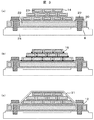
比較例1の平面模式図を図10に示す。比較例1の制御ユニットとフレキシブル基板を半田で接続している。フレキシブル基板37の銅配線は厚さ0.035mmの銅箔をエッチングで所定形状にパターン形成したものを用いた。
比較例2の断面模式図を11に示す。金属銅板をプレスで打ちぬき作製したバスバー33をナイロンの射出成型で被覆した。このときナイロン32の被覆厚さが1mmとなり薄肉化するのが困難であった。このため、配線のレイアウト自由度が低下し、小型の変速機内に設置するのが難しい問題があった。

2 チップコンデンサ
3 チップ抵抗
4 基板
5,6 リードフレーム
7 封止材
8 固定構造
9 角型配線材
10 金属平板
11 金型
12 固定穴
13 マスキング
14 絶縁被覆
15 制御ユニット
16 接着材
17 油圧センサー
18 ソレノイド
19 バルブボディ
20 コネクタ
21 タイバー
22 厚手の角型配線材
23 薄手の角型配線材
24 変速機筐体
25 円形の固定穴
26 楕円形の固定穴
27 U字型の固定穴
28 タイバーカット
29 ネジ
30 ワッシャー
31 固定板
32 ナイロン
33 バスバー
34 支持板
35 絶縁材を分散した溶液
36 絶縁材
37 フレキシブル基板
38 金属製線材
Claims (9)
- 制御信号発生部品と、前記制御信号発生部品の制御信号によって制御される被制御部品とを接続する角型配線材とを備え、導電性筐体内に設置される機電一体型電子制御装置において、
少なくとも前記配線材は、固定穴を有し、固定穴を含む表面が絶縁被覆され、前記固定穴は導電性筐体に絶縁性を保ち、かつ機械的に固定できることを特徴とする機電一体型電子制御装置。 - 請求項1において、前記導電性製筐体が変速機筐体であることを特徴とする変速機制御装置。
- 請求項1において、前記角型配線材は、金属平板を固定穴を有する配線形状にプレスで打ち抜いた後、折り曲げ加工を行い、導電性が必要な場所にマスキングを施し、絶縁材が分散した溶液にディップした後、加熱乾燥処理することで、固定穴を含む表面を絶縁材で被覆して形成されたことを特徴とする変速機制御装置。
- 請求項1において、前記角型配線材は、金属製線材を固定穴形状及び配線形状に布線した後、プレスで平坦化し導電性が必要な場所にマスキングを施し、絶縁材が分散した溶液にディップした後、加熱乾燥処理することで、固定穴を含む表面を絶縁材で被覆して形成されたことを特徴とする変速機制御装置。
- 請求項2おいて、前記角型配線材が複数の厚さを有し、厚手の角型配線材上に薄手の角型配線材を重ねたことを特徴とする変速機制御装置。
- 請求項2において、前記角型配線材の固定穴は少なくとも前記制御信号発生部品及び前記被制御部品近傍に設け、前記制御信号発生部品と前記被制御部品を接続する間の前記角型配線材の一部に幅狭の領域を設けた事を特徴とする変速機制御装置。
- 請求項2において、前記絶縁被覆はイミド基を有する高分子材料によりなされていることを特徴とする変速機制御装置。
- 請求項2において、前記角型配線材は銅,鉄,アルミのいずれか2種又は3種を素材として用いたことを特徴とする変速機制御装置。
- 請求項2において、前記固定穴はU字形状であることを特徴とする変速機制御装置。
Priority Applications (4)
| Application Number | Priority Date | Filing Date | Title |
|---|---|---|---|
| JP2009225899A JP5188483B2 (ja) | 2009-09-30 | 2009-09-30 | 変速制御装置及び機電一体型電子制御装置 |
| US12/831,737 US8339795B2 (en) | 2009-09-30 | 2010-07-07 | Transmission control apparatus and mechanically and electrically integrated type electronic control apparatus |
| EP10007686A EP2306798A1 (en) | 2009-09-30 | 2010-07-23 | Transmission control apparatus and mechanically and electrically integrated type electronic control apparatus |
| CN2010102506132A CN102035442B (zh) | 2009-09-30 | 2010-08-10 | 变速机控制装置和机电一体型电子控制装置 |
Applications Claiming Priority (1)
| Application Number | Priority Date | Filing Date | Title |
|---|---|---|---|
| JP2009225899A JP5188483B2 (ja) | 2009-09-30 | 2009-09-30 | 変速制御装置及び機電一体型電子制御装置 |
Publications (2)
| Publication Number | Publication Date |
|---|---|
| JP2011074983A JP2011074983A (ja) | 2011-04-14 |
| JP5188483B2 true JP5188483B2 (ja) | 2013-04-24 |
Family
ID=43513647
Family Applications (1)
| Application Number | Title | Priority Date | Filing Date |
|---|---|---|---|
| JP2009225899A Active JP5188483B2 (ja) | 2009-09-30 | 2009-09-30 | 変速制御装置及び機電一体型電子制御装置 |
Country Status (4)
| Country | Link |
|---|---|
| US (1) | US8339795B2 (ja) |
| EP (1) | EP2306798A1 (ja) |
| JP (1) | JP5188483B2 (ja) |
| CN (1) | CN102035442B (ja) |
Families Citing this family (4)
| Publication number | Priority date | Publication date | Assignee | Title |
|---|---|---|---|---|
| JP2011252549A (ja) * | 2010-06-02 | 2011-12-15 | Denso Corp | 自動変速機の制御装置 |
| JP5829110B2 (ja) * | 2011-11-29 | 2015-12-09 | 日立オートモティブシステムズ株式会社 | 電子モジュール |
| WO2014067749A1 (en) * | 2012-11-02 | 2014-05-08 | Evonik Industries Ag | Process for preparing low sulfur dispersant polymers |
| JP6417349B2 (ja) * | 2016-03-09 | 2018-11-07 | 矢崎総業株式会社 | コネクタモジュール及び液圧制御装置 |
Family Cites Families (12)
| Publication number | Priority date | Publication date | Assignee | Title |
|---|---|---|---|---|
| US3639680A (en) * | 1970-12-07 | 1972-02-01 | Cutler Hammer Inc | Insulated bus bar assembly |
| JPH03285570A (ja) | 1990-03-30 | 1991-12-16 | Mitsubishi Electric Corp | インバータ装置 |
| US6270889B1 (en) * | 1998-01-19 | 2001-08-07 | Mitsui Mining & Smelting Co., Ltd. | Making and using an ultra-thin copper foil |
| US6741245B1 (en) * | 1999-04-23 | 2004-05-25 | Mitsubishi Electric Research Laboratories, Inc. | Method for decorating a virtual model |
| JP3751487B2 (ja) * | 1999-10-29 | 2006-03-01 | 株式会社オートネットワーク技術研究所 | 平型導体配線板の回路導体の接続方法及び接続構造 |
| FR2801763B1 (fr) * | 1999-11-30 | 2002-02-15 | Sagem | Module electronique de puissance et procede de fabrication d'un tel module |
| JP2003282171A (ja) * | 2002-03-27 | 2003-10-03 | Yazaki Corp | 電気的接続部 |
| JP2004032960A (ja) * | 2002-06-28 | 2004-01-29 | Yazaki Corp | 電気接続箱とその製造方法 |
| JP3815456B2 (ja) * | 2003-04-09 | 2006-08-30 | トヨタ自動車株式会社 | ハイブリッド車両における高圧電線の配策構造 |
| JP2006187122A (ja) | 2004-12-27 | 2006-07-13 | Auto Network Gijutsu Kenkyusho:Kk | 回路構成体 |
| JP4732789B2 (ja) | 2005-04-28 | 2011-07-27 | 株式会社オートネットワーク技術研究所 | スイッチングユニット |
| DE102007042593B4 (de) | 2007-09-07 | 2018-10-31 | Continental Automotive Gmbh | Modul für eine integrierte Steuerelektronik mit vereinfachtem Aufbau |
-
2009
- 2009-09-30 JP JP2009225899A patent/JP5188483B2/ja active Active
-
2010
- 2010-07-07 US US12/831,737 patent/US8339795B2/en not_active Expired - Fee Related
- 2010-07-23 EP EP10007686A patent/EP2306798A1/en not_active Withdrawn
- 2010-08-10 CN CN2010102506132A patent/CN102035442B/zh not_active Expired - Fee Related
Also Published As
| Publication number | Publication date |
|---|---|
| EP2306798A1 (en) | 2011-04-06 |
| US20110075334A1 (en) | 2011-03-31 |
| US8339795B2 (en) | 2012-12-25 |
| JP2011074983A (ja) | 2011-04-14 |
| CN102035442A (zh) | 2011-04-27 |
| CN102035442B (zh) | 2013-07-10 |
Similar Documents
| Publication | Publication Date | Title |
|---|---|---|
| JP4607995B2 (ja) | 電力用半導体装置 | |
| JP4408444B2 (ja) | Lcモジュール構造を用いた電子制御装置 | |
| US10829064B2 (en) | Electronic control device | |
| JP6554097B2 (ja) | 電気接続装置 | |
| JP2016502279A (ja) | プラスチックで被覆された電子回路を備えた電子モジュールおよび該電子モジュールを製造する方法 | |
| JP6561129B2 (ja) | 電子制御装置またはその製造方法 | |
| JP5450192B2 (ja) | パワーモジュールとその製造方法 | |
| JP6246051B2 (ja) | 電力半導体装置およびその製造方法 | |
| JP5188483B2 (ja) | 変速制御装置及び機電一体型電子制御装置 | |
| CN104066291A (zh) | 外壳及具有该外壳的电源模块 | |
| WO2018193828A1 (ja) | 金属部材付き基板、回路構成体及び電気接続箱 | |
| CN107006126B (zh) | 利用按压接触三明治模块技术的特别是用于机动车传动装置控制设备的电子装置模块 | |
| JP5939895B2 (ja) | 車載用電子制御装置 | |
| JP2011077463A (ja) | 電力変換装置、それを用いた回転電機、及び半導体パワーモジュールの製造方法 | |
| JP5449237B2 (ja) | 基板および基板の製造方法 | |
| CN1870858A (zh) | 用于电气设备的散热装置 | |
| CN112056011B (zh) | 电路结构体及电连接箱 | |
| JP6391430B2 (ja) | 電子制御装置およびその製造方法 | |
| JP2003218317A (ja) | 半導体電力変換装置 | |
| JP2008147432A (ja) | 電子回路装置及び電力変換装置及び電子回路装置の製造方法 | |
| JP2013165207A (ja) | 導線付き回路基板及びその製造方法 | |
| CN111602237A (zh) | 具有得到改进的电接触的线路基座装置 | |
| JP2020047840A (ja) | 電子制御装置 | |
| JP2019140321A (ja) | 電子部品搭載用基板、及び、電子デバイス | |
| EP3474638A1 (en) | Ddr electronic module assembly |
Legal Events
| Date | Code | Title | Description |
|---|---|---|---|
| A621 | Written request for application examination |
Free format text: JAPANESE INTERMEDIATE CODE: A621 Effective date: 20111228 |
|
| A521 | Request for written amendment filed |
Free format text: JAPANESE INTERMEDIATE CODE: A523 Effective date: 20111228 |
|
| TRDD | Decision of grant or rejection written | ||
| A01 | Written decision to grant a patent or to grant a registration (utility model) |
Free format text: JAPANESE INTERMEDIATE CODE: A01 Effective date: 20121225 |
|
| A977 | Report on retrieval |
Free format text: JAPANESE INTERMEDIATE CODE: A971007 Effective date: 20121228 |
|
| A61 | First payment of annual fees (during grant procedure) |
Free format text: JAPANESE INTERMEDIATE CODE: A61 Effective date: 20130122 |
|
| FPAY | Renewal fee payment (event date is renewal date of database) |
Free format text: PAYMENT UNTIL: 20160201 Year of fee payment: 3 |
|
| R150 | Certificate of patent or registration of utility model |
Ref document number: 5188483 Country of ref document: JP Free format text: JAPANESE INTERMEDIATE CODE: R150 Free format text: JAPANESE INTERMEDIATE CODE: R150 |
|
| S533 | Written request for registration of change of name |
Free format text: JAPANESE INTERMEDIATE CODE: R313533 |
|
| R350 | Written notification of registration of transfer |
Free format text: JAPANESE INTERMEDIATE CODE: R350 |
|
| R250 | Receipt of annual fees |
Free format text: JAPANESE INTERMEDIATE CODE: R250 |
|
| R250 | Receipt of annual fees |
Free format text: JAPANESE INTERMEDIATE CODE: R250 |