[go: up one dir, main page]

JP4589987B2 - Interlocking counter and interlocking device - Google Patents

Interlocking counter and interlocking device Download PDF

Info

Publication number
JP4589987B2
JP4589987B2 JP2008163569A JP2008163569A JP4589987B2 JP 4589987 B2 JP4589987 B2 JP 4589987B2 JP 2008163569 A JP2008163569 A JP 2008163569A JP 2008163569 A JP2008163569 A JP 2008163569A JP 4589987 B2 JP4589987 B2 JP 4589987B2
Authority
JP
Japan
Prior art keywords
image
signal
interlocking
logic gate
counter
Prior art date
Legal status (The legal status is an assumption and is not a legal conclusion. Google has not performed a legal analysis and makes no representation as to the accuracy of the status listed.)
Expired - Fee Related
Application number
JP2008163569A
Other languages
Japanese (ja)
Other versions
JP2008289179A (en
Inventor
義明 味岡
Original Assignee
株式会社エッチャンデス
Priority date (The priority date is an assumption and is not a legal conclusion. Google has not performed a legal analysis and makes no representation as to the accuracy of the date listed.)
Filing date
Publication date
Application filed by 株式会社エッチャンデス filed Critical 株式会社エッチャンデス
Priority to JP2008163569A priority Critical patent/JP4589987B2/en
Publication of JP2008289179A publication Critical patent/JP2008289179A/en
Application granted granted Critical
Publication of JP4589987B2 publication Critical patent/JP4589987B2/en
Anticipated expiration legal-status Critical
Expired - Fee Related legal-status Critical Current

Links

Images

Classifications

    • HELECTRICITY
    • H03ELECTRONIC CIRCUITRY
    • H03KPULSE TECHNIQUE
    • H03K21/00Details of pulse counters or frequency dividers
    • H03K21/40Monitoring; Error detection; Preventing or correcting improper counter operation
    • H03K21/406Synchronisation of counters
    • GPHYSICS
    • G06COMPUTING OR CALCULATING; COUNTING
    • G06TIMAGE DATA PROCESSING OR GENERATION, IN GENERAL
    • G06T7/00Image analysis
    • G06T7/70Determining position or orientation of objects or cameras
    • G06T7/73Determining position or orientation of objects or cameras using feature-based methods
    • G06T7/74Determining position or orientation of objects or cameras using feature-based methods involving reference images or patches
    • GPHYSICS
    • G06COMPUTING OR CALCULATING; COUNTING
    • G06VIMAGE OR VIDEO RECOGNITION OR UNDERSTANDING
    • G06V10/00Arrangements for image or video recognition or understanding
    • G06V10/20Image preprocessing
    • G06V10/24Aligning, centring, orientation detection or correction of the image
    • GPHYSICS
    • G06COMPUTING OR CALCULATING; COUNTING
    • G06VIMAGE OR VIDEO RECOGNITION OR UNDERSTANDING
    • G06V10/00Arrangements for image or video recognition or understanding
    • G06V10/20Image preprocessing
    • G06V10/32Normalisation of the pattern dimensions
    • GPHYSICS
    • G06COMPUTING OR CALCULATING; COUNTING
    • G06VIMAGE OR VIDEO RECOGNITION OR UNDERSTANDING
    • G06V10/00Arrangements for image or video recognition or understanding
    • G06V10/94Hardware or software architectures specially adapted for image or video understanding
    • G06V10/955Hardware or software architectures specially adapted for image or video understanding using specific electronic processors
    • GPHYSICS
    • G06COMPUTING OR CALCULATING; COUNTING
    • G06VIMAGE OR VIDEO RECOGNITION OR UNDERSTANDING
    • G06V40/00Recognition of biometric, human-related or animal-related patterns in image or video data
    • G06V40/10Human or animal bodies, e.g. vehicle occupants or pedestrians; Body parts, e.g. hands
    • G06V40/16Human faces, e.g. facial parts, sketches or expressions
    • G06V40/161Detection; Localisation; Normalisation
    • G06V40/162Detection; Localisation; Normalisation using pixel segmentation or colour matching
    • HELECTRICITY
    • H03ELECTRONIC CIRCUITRY
    • H03KPULSE TECHNIQUE
    • H03K21/00Details of pulse counters or frequency dividers
    • H03K21/38Starting, stopping or resetting the counter
    • HELECTRICITY
    • H04ELECTRIC COMMUNICATION TECHNIQUE
    • H04NPICTORIAL COMMUNICATION, e.g. TELEVISION
    • H04N23/00Cameras or camera modules comprising electronic image sensors; Control thereof
    • H04N23/60Control of cameras or camera modules
    • H04N23/665Control of cameras or camera modules involving internal camera communication with the image sensor, e.g. synchronising or multiplexing SSIS control signals
    • HELECTRICITY
    • H04ELECTRIC COMMUNICATION TECHNIQUE
    • H04NPICTORIAL COMMUNICATION, e.g. TELEVISION
    • H04N25/00Circuitry of solid-state image sensors [SSIS]; Control thereof
    • HELECTRICITY
    • H04ELECTRIC COMMUNICATION TECHNIQUE
    • H04NPICTORIAL COMMUNICATION, e.g. TELEVISION
    • H04N25/00Circuitry of solid-state image sensors [SSIS]; Control thereof
    • H04N25/47Image sensors with pixel address output; Event-driven image sensors; Selection of pixels to be read out based on image data
    • HELECTRICITY
    • H04ELECTRIC COMMUNICATION TECHNIQUE
    • H04NPICTORIAL COMMUNICATION, e.g. TELEVISION
    • H04N25/00Circuitry of solid-state image sensors [SSIS]; Control thereof
    • H04N25/70SSIS architectures; Circuits associated therewith
    • H04N25/703SSIS architectures incorporating pixels for producing signals other than image signals
    • H04N25/707Pixels for event detection
    • HELECTRICITY
    • H04ELECTRIC COMMUNICATION TECHNIQUE
    • H04NPICTORIAL COMMUNICATION, e.g. TELEVISION
    • H04N25/00Circuitry of solid-state image sensors [SSIS]; Control thereof
    • H04N25/70SSIS architectures; Circuits associated therewith
    • H04N25/703SSIS architectures incorporating pixels for producing signals other than image signals
    • H04N25/708Pixels for edge detection
    • HELECTRICITY
    • H04ELECTRIC COMMUNICATION TECHNIQUE
    • H04NPICTORIAL COMMUNICATION, e.g. TELEVISION
    • H04N25/00Circuitry of solid-state image sensors [SSIS]; Control thereof
    • H04N25/70SSIS architectures; Circuits associated therewith
    • H04N25/71Charge-coupled device [CCD] sensors; Charge-transfer registers specially adapted for CCD sensors
    • H04N25/73Charge-coupled device [CCD] sensors; Charge-transfer registers specially adapted for CCD sensors using interline transfer [IT]
    • HELECTRICITY
    • H04ELECTRIC COMMUNICATION TECHNIQUE
    • H04NPICTORIAL COMMUNICATION, e.g. TELEVISION
    • H04N25/00Circuitry of solid-state image sensors [SSIS]; Control thereof
    • H04N25/70SSIS architectures; Circuits associated therewith
    • H04N25/76Addressed sensors, e.g. MOS or CMOS sensors
    • H04N25/78Readout circuits for addressed sensors, e.g. output amplifiers or A/D converters
    • HELECTRICITY
    • H04ELECTRIC COMMUNICATION TECHNIQUE
    • H04NPICTORIAL COMMUNICATION, e.g. TELEVISION
    • H04N25/00Circuitry of solid-state image sensors [SSIS]; Control thereof
    • H04N25/70SSIS architectures; Circuits associated therewith
    • H04N25/79Arrangements of circuitry being divided between different or multiple substrates, chips or circuit boards, e.g. stacked image sensors
    • GPHYSICS
    • G06COMPUTING OR CALCULATING; COUNTING
    • G06TIMAGE DATA PROCESSING OR GENERATION, IN GENERAL
    • G06T2207/00Indexing scheme for image analysis or image enhancement
    • G06T2207/30Subject of image; Context of image processing
    • G06T2207/30196Human being; Person
    • G06T2207/30201Face

Landscapes

  • Engineering & Computer Science (AREA)
  • Multimedia (AREA)
  • Signal Processing (AREA)
  • Physics & Mathematics (AREA)
  • General Physics & Mathematics (AREA)
  • Theoretical Computer Science (AREA)
  • General Health & Medical Sciences (AREA)
  • Health & Medical Sciences (AREA)
  • Computer Vision & Pattern Recognition (AREA)
  • Oral & Maxillofacial Surgery (AREA)
  • Human Computer Interaction (AREA)
  • Software Systems (AREA)
  • Image Processing (AREA)
  • Image Analysis (AREA)
  • Image Input (AREA)
  • Transforming Light Signals Into Electric Signals (AREA)
  • Closed-Circuit Television Systems (AREA)

Description

本発明は、物体を探索及び認識する視覚装置に使用し、幾何解析手段などの局所並列画像処理を実行する複数の配列演算ユニット及び複数の仮想配列演算ユニットを駆動する、連動式カウンタ及び連動装置に関する。   The present invention is used in a visual device for searching and recognizing an object, and drives a plurality of array operation units and a plurality of virtual array operation units that execute local parallel image processing such as geometric analysis means and the like. About.

移動カメラを制御し、画像処理をする装置として、本発明者はこれまで視覚装置(visu al device)を開発してきた(例えば、特開2001−43385、特開2001−101403、特開2001−148006、特開2001−148022、特開2001−148024、国際公開番号WO00/16259参照)。この視覚装置は移動カメラ(moving camera)のパン、チルト及びズームの機構を制御することにより、物体を探索し、物体の画像処理を行うものである。視覚装置が行う画像処理の大半が局所処理であり、しかもこれらの局所処理(local processing)は二次元格子状に配列された複数の配列演算ユニット(array operation units)によって並列に実行され得る。しかしながらこの視覚装置には、主に4つの問題があった。第一に、物体/背景分離手段(figure/ground separ ation means)は、非線形振動子(nonlinear oscillator)を用いて少なくとも1つの物体領域(object area)と背景領域(bac kground area)を分離するために、膨大な計算量を必要とした。第二に、パターンマッチング手段(pattern matching means)は、物体の色とパターンが混在した正規化画像(normalized image)を正しく認識するために、多数のテンプレート画像(template images)を必要とした。第三に、幾何解析手段(geometrical analysis means)は、動画像中の物体の大まかな形を検出するために、フーリエ変換、アフィン変換及びハフ変換のような大域処理を行わなければならなかった。第四に、領域正規化手段(area normalization means)は、正規化画像の画素間を補間するために、自然数による除算を実行するための除算器を備えたプロセッサを必要とするか、又はこの自然数の逆数を記憶するためのルックアップテーブルを必要とした。そのため、これらの手段は、視覚装置を有する高性能イメージセンサの製造にとって大きな障害であった。   As an apparatus for controlling a moving camera and performing image processing, the present inventor has so far developed a visual device (for example, JP 2001-43385, JP 2001-101403, JP 2001-148006). JP-A-2001-148022, JP-A-2001-148024, International Publication No. WO00 / 16259). This visual device searches for an object and performs image processing of the object by controlling pan, tilt and zoom mechanisms of a moving camera. Most of the image processing performed by the visual device is local processing, and these local processing can be performed in parallel by a plurality of array operation units arranged in a two-dimensional grid. However, this visual device has four main problems. First, an object / background separation means separates at least one object area and a background area using a non-linear oscillator. In addition, a huge amount of calculation was required. Second, the pattern matching means requires a large number of template images in order to correctly recognize a normalized image in which the color and pattern of the object are mixed. Third, the geometric analysis means has to perform global processing such as Fourier transform, affine transform, and Hough transform in order to detect the rough shape of the object in the moving image. Fourth, the area normalization means requires a processor with a divider for performing division by natural numbers in order to interpolate between pixels of the normalized image, or this natural number We needed a look-up table to store the reciprocal of. Therefore, these means have been a major obstacle for the production of high performance image sensors with visual devices.

まず、従来の物体/背景分離手段において、各々の非線形振動子は、外乱(externa l noise)として乱数を用いるか、又は入力された形成エッジ情報画像の1画素を構成する形成エッジ情報を用いていた。したがって、形成エッジ情報画像によって区分される物体領域又は背景領域に含まれる非線形振動子と、外乱と、の間に相関はない。その結果、各々の非線形振動子は、近傍にある複数の非線形振動子の位相が適当な組み合せになるまで、自らの位相をこれらの非線形振動子の位相からずらすことができなかった。このことが、物体/背景分離手段の計算量が増加する要因であった。しかしながら、視覚装置は、位置/大きさ検出手段を用いることにより、形成エッジ情報画像によって区分される物体領域のおおよその重心位置及びその大きさを表す重複情報画像を生成することができる。そこで、各々の非線形振動子が、重複情報画像のうち、対応する画素を構成する重複情報を乱数として入力することにより、物体領域に含まれる各々の非線形振動子は、おおよその重心位置から周囲に向けて順番に位相をずらす。   First, in the conventional object / background separation means, each nonlinear vibrator uses a random number as external noise, or uses formation edge information constituting one pixel of the input formation edge information image. It was. Therefore, there is no correlation between the nonlinear vibrator included in the object region or the background region divided by the formed edge information image and the disturbance. As a result, each nonlinear oscillator could not shift its own phase from the phase of these nonlinear oscillators until the phases of a plurality of nearby nonlinear oscillators became an appropriate combination. This is a factor that increases the calculation amount of the object / background separation means. However, by using the position / size detection means, the visual device can generate an overlapping information image representing the approximate center of gravity position and the size of the object region divided by the formed edge information image. Therefore, each nonlinear vibrator inputs the overlapping information constituting the corresponding pixel in the overlapping information image as a random number, so that each nonlinear vibrator included in the object region moves from the approximate center of gravity position to the periphery. Shift the phase in order.

これらのことを考慮すると、位置/大きさ検出手段が形成エッジ情報画像によって区分される物体領域のおおよその重心位置及びその大きさを検出することにより、物体/背景分離手段は、従来に比べて高速に物体領域と背景領域を分離することができると期待される。   Considering these, the position / size detection means detects the approximate center of gravity position and the size of the object area divided by the formed edge information image, so that the object / background separation means It is expected that the object area and the background area can be separated at high speed.

次に、従来の視覚装置において、パターンマッチング手段はデジタル画像のうち、物体領域に相当する分離物体領域を正規化した正規化画像をパターンマッチングするために、非常に多くの数のテンプレート画像を必要とした。この理由は、正規化画像が一般にノイズを含んだ多帯域画像であり、しかもパターンマッチング手段が、正規化画像が表す物体の色及びパターンを区別せずに、この正規化画像と多数のテンプレート画像を比較したからである。つまりテンプレート画像は物体の色及びパターンの組み合せの数だけ必要になる。そこで正規化画像が表す物体の色及びパターンを別々にパターンマッチングする場合を考えてみる。まず、物体の色を、正規化画像の各画素が表す色のうち画素数が最も多い色とする。このときパターンマッチング手段は、検出すべき複数の色のうちの相異なる1つの色によって塗り潰されたテンプレート画像を、検出すべき色の数だけ用意することにより、正規化画像が表す物体の色を検出することができる。しかもデジタル画像中の物体の位置及び大きさが変っても、パターンマッチング手段は、分離物体領域に含まれる各画素の色を複数のテンプレート画像と比較することにより、この物体の色を検出することができるので、分離物体領域を正規化する必要もない。一方で、物体のパターンに関しては、分離物体領域に対する正規化画像の代りに、エッジ情報形成手段が分離物体領域から一旦形成エッジ情報画像を生成し、その後、幾何解析手段が形成エッジ情報画像から生成した画像に対する正規化画像を用いるものとする。このとき正規化画像のうち少なくとも1画素には、その周辺にある物体のパターンの一部を表す形及び大きさが記されているので、パターンマッチング手段は、物体領域の位置及び大きさに関係なく、この正規化画像に最も類似したテンプレート画像を容易に選択することができる。これらのことを考慮すると、視覚装置が、複数のパターンマッチング手段を用いて、物体領域が表す物体の色及びパターンを別々に処理することにより、色及びパターンに対する複数のパターンマッチング手段は、それぞれテンプレート画像の数を大幅に削減することができると期待される。   Next, in the conventional visual apparatus, the pattern matching means requires a very large number of template images in order to pattern-match the normalized image obtained by normalizing the separated object region corresponding to the object region. It was. The reason for this is that the normalized image is generally a multiband image including noise, and the pattern matching means does not distinguish between the color and pattern of the object represented by the normalized image, and the normalized image and a number of template images. This is because of the comparison. That is, as many template images as the number of combinations of object colors and patterns are required. Consider a case where the color and pattern of the object represented by the normalized image are separately subjected to pattern matching. First, the color of the object is the color with the largest number of pixels among the colors represented by the pixels of the normalized image. At this time, the pattern matching means prepares template images filled with one different color among a plurality of colors to be detected by the number of colors to be detected, thereby obtaining the color of the object represented by the normalized image. Can be detected. Moreover, even if the position and size of the object in the digital image changes, the pattern matching means detects the color of this object by comparing the color of each pixel included in the separated object region with a plurality of template images. Therefore, it is not necessary to normalize the separated object area. On the other hand, with respect to the object pattern, instead of the normalized image for the separated object area, the edge information forming means once generates a formed edge information image from the separated object area, and then the geometric analysis means is generated from the formed edge information image. It is assumed that a normalized image for the obtained image is used. At this time, since at least one pixel of the normalized image has a shape and size representing a part of the pattern of the object around it, the pattern matching means is related to the position and size of the object region. Instead, the template image most similar to the normalized image can be easily selected. Taking these into consideration, the visual device uses a plurality of pattern matching means to separately process the color and pattern of the object represented by the object region, so that the plurality of pattern matching means for the color and the pattern are respectively templates. It is expected that the number of images can be greatly reduced.

次に、従来の幾何解析手段は、テンプレート画像の数が多くなった場合、パターンマッチング手段の計算量を低減するために、フーリエ変換を用いて動画像中の物体のエッジ情報から輪郭だけを抽出することと、アフィン変換を用いて動画像中の物体の輪郭の大きさを正規化することと、ハフ変換を用いて動画像中の物体の形状を特定することと、を適切に組み合せて利用していた。しかしながら、これらの変換は、画像を厳密に処理する上に、大域処理であるので、視覚装置のハードウェアへの実装には適さなかった。そこで、幾何解析手段が物体の大まかな形を検出することに着目すると、この幾何解析手段が、細切れにされたこの物体の輪郭の断片から位置及び傾きを求め、この傾きをこの物体の輪郭の重心に集めることができれば、この幾何解析手段は、この物体の大まかな形を検出することができる。   Next, when the number of template images increases, the conventional geometric analysis means extracts only the contour from the edge information of the object in the moving image using Fourier transform in order to reduce the calculation amount of the pattern matching means. Using the affine transformation, normalizing the size of the contour of the object in the moving image, and identifying the shape of the object in the moving image using the Hough transform. Was. However, since these conversions are global processing in addition to processing images strictly, they are not suitable for mounting on a visual device hardware. Therefore, paying attention to the fact that the geometric analysis means detects the rough shape of the object, the geometric analysis means obtains the position and the inclination from the fragment of the outline of the object which has been cut into pieces, and this inclination is calculated from the outline of the object. If it can be collected at the center of gravity, the geometric analysis means can detect the rough shape of the object.

これらのことを考慮すると、傾きを検出する手段が形成エッジ情報画像(formed edge−information image)から物体の輪郭を表す複数の線分の長さ及び傾き角度を計算し、さらにこれらの線分の長さ及び傾き角度を、傾き角度毎に物体の輪郭の重心方向に移動すると同時にこれらの線分の移動距離を計算することにより、幾何解析手段は画像処理に適したような物体の位置及び形を検出することができると期待される。しかも物体の輪郭線は既に複数の独立した線分に分割されているので、線分が位置する画素をその近傍との間で一定の制約条件を満たしながら独立に移動させれば、幾何解析手段は少ないハードウェア量と計算量で物体の位置及び形を検出することができると期待される。   Considering these, the means for detecting the inclination calculates the length and inclination angle of a plurality of line segments representing the contour of the object from the formed edge-information image, and further, these line segments. By moving the length and inclination angle in the direction of the center of gravity of the contour of the object for each inclination angle, and simultaneously calculating the movement distance of these line segments, the geometric analysis means can detect the position and shape of the object suitable for image processing. Is expected to be detected. Moreover, since the contour line of the object has already been divided into a plurality of independent line segments, if the pixel where the line segment is located is moved independently while satisfying a certain constraint condition with the vicinity thereof, the geometric analysis means Is expected to be able to detect the position and shape of an object with a small amount of hardware and computation.

最後に、領域正規化手段は、一旦物体領域に相当するデジタル画像中の分離物体領域(se gmented object area)に含まれる各画素を、互いの距離がおおよそ等しくなるように、デジタル画像全面に移動させた後、これらの画素の間に位置する画素を、近傍の画素の平均によって補間することにより、領域正規化手段はデジタル画像のサイズと等しいサイズの正規化画像を生成する。したがって、領域正規化手段は、画素間を補間するために自然数による除算、又はこの自然数の逆数の乗算を実行しなければならない。このように領域正規化手段が補間する理由は、以下の通りである。第一に、大きさ及び位置が異なる複数の分離物体領域が同じ物体を表す場合、一旦バラバラになった分離物体領域の各画素から分離物体領域のパターンを再構成しなければ、正規化画像の出力先であるパターンマッチング手段が同じ物体に対して多数のテンプレート画像を有しなければならないからである。第二に、デジタル画像が一般にノイズを含む多帯域画像であるために、一旦バラバラになった分離物体領域の画素間を補間をすることにより、正規化画像と、この正規画像と同じ種類の物体の表すテンプレート画像と、の間の類似度が増すからである。しかしながら、前述のように、パターンマッチング手段が、分離物体領域に対する正規化画像の代りに、エッジ情報形成手段が分離物体領域から一旦形成エッジ情報画像を生成し、その後幾何解析手段が形成エッジ情報画像から生成した画像に対する正規化画像を用いる場合、正規化画像のうち少なくとも1画素に、その周辺にある物体のパターンの一部を表す形及び大きさが記されている。したがって、領域正規化手段が補間をしなくても、パターンマッチング手段は複数のテンプレート画像の中から正規化画像に最も類似したテンプレート画像を選択することができる。   Finally, the region normalization means moves each pixel included in the segmented object area in the digital image corresponding to the object region to the entire surface of the digital image so that the distances between them are approximately equal to each other. Then, by interpolating the pixels located between these pixels with the average of neighboring pixels, the region normalizing means generates a normalized image having a size equal to the size of the digital image. Therefore, the region normalizing means must perform division by a natural number or multiplication of the reciprocal of this natural number in order to interpolate between pixels. The reason why the region normalizing means interpolates in this way is as follows. First, when a plurality of separated object regions of different sizes and positions represent the same object, the normalized image of the normalized image must be reconstructed from each pixel of the separated object region once separated. This is because the pattern matching means as the output destination must have a large number of template images for the same object. Second, since a digital image is generally a multi-band image including noise, a normalized image and an object of the same type as the normal image are obtained by interpolating between pixels of the separated object region once separated. This is because the degree of similarity between the template image represented by and increases. However, as described above, instead of the normalized image for the separated object area, the pattern matching means once generates the formed edge information image from the separated object area, and then the geometric analysis means forms the formed edge information image. In the case of using a normalized image for an image generated from the above, at least one pixel of the normalized image has a shape and a size representing a part of the pattern of an object around it. Therefore, even if the region normalizing means does not perform interpolation, the pattern matching means can select a template image most similar to the normalized image from among a plurality of template images.

これらのことを考慮すると、領域正規化手段が補間をしなくても、パターンマッチング手段は物体領域が表す物体のパターンを選択することができると期待される。
さて、この視覚装置は移動カメラのパン、チルト及びズームの機構を制御することにより、物体を探索し、物体の画像処理を行うものである。視覚装置が行う画像処理の大半が局所処理であり、しかもこれらの局所処理は二次元格子状に配列された配列演算ユニットによって並列に実行される。配列演算ユニットをLSIに実装する場合、個々の配列演算ユニットは、送達及び受領という信号を用いることにより、隣接する配列演算ユニットと非同期に通信できるように設計されている。これにより、配線パターンは極めて単純になり、しかも配線長は短くなるので、LSIはトランジスタの実装面積を増やしながら消費電力を低下させることができ、しかも全ての配列演算ユニットは必ずしも同期する必要がない。
Considering these, it is expected that the pattern matching means can select the pattern of the object represented by the object area even if the area normalizing means does not perform interpolation.
The visual device searches for an object and performs image processing of the object by controlling the pan, tilt, and zoom mechanisms of the moving camera. Most of the image processing performed by the visual device is local processing, and these local processing is executed in parallel by an array operation unit arranged in a two-dimensional grid. When an array operation unit is mounted on an LSI, each array operation unit is designed to communicate asynchronously with an adjacent array operation unit by using signals of delivery and reception. As a result, the wiring pattern becomes extremely simple and the wiring length is shortened, so that the LSI can reduce the power consumption while increasing the mounting area of the transistors, and all the array operation units do not necessarily have to be synchronized. .

ところで、従来の配列演算ユニットには主に4つの問題があった。第一の問題は、送達を送信したコントローラにおいて送達を送信してから受領を受信するまでの時間が長くなることである。この原因は、送達を受信したコントローラが、計算データ、種別、水平方向の転送回数及び垂直方向の転送回数を入力するまで受領を返信しないことにある。そこで従来の配列演算ユニットでは、送達を送信したコントローラの上下左右の受領ステータスが確実に更新されるまで、プロセッサは待たなければならなかった。しかしながら、この方法ではコントローラが折角非同期通信をしていてもプロセッサが無駄に時間を潰さなければならない。第二の問題は、計算データの転送順番が不規則であるので、未転送の計算データと転送済の計算データの区別が難しいことである。この原因は全ての配列演算ユニットが独立に動作することにある。そこで従来の配列演算ユニットでは、メモリが受信した計算データを転送すべき送達フラグと一緒に記憶し、一方でプロセッサはメモリに記憶された全ての送達フラグを常に検査して計算データを転送した後、転送された計算データに関連する送達フラグを更新していた。しかしながら、この方法ではプロセッサは既に転送した計算データの送達フラグでも繰り返し検査しなければならない。第三の問題は、計算データが同時に3方向に転送される場合、プロセッサがコントローラに計算データを書き込める割合が低いことである。この原因は、コントローラが4近傍の配列演算ユニットに対して一度に1個の計算データしか送信できないことにある。そこで従来の配列演算ユニットでは、送達フラグによって指定された配列演算ユニットの数が多くなればなるほど、プロセッサは次の計算データをコントローラに書き込めるようになるまで長時間待たなければならなかった。第四の問題は、計算データが同時に3方向に転送される場合、計算データを受信する配列演算ユニットは、この計算データの水平方向の転送回数及び垂直方向の転送回数が同じになる2個の配列演算ユニットを区別することが難しいことである。この原因は、コントローラが水平方向の転送回数及び垂直方向の転送回数を非負の整数でしか通信しないことにある。そこで従来の配列演算ユニットでは、計算データの送信元である2個の配列演算ユニットに優先順位が付けられ、配列演算ユニットは必ず優先順位が高い配列演算ユニットの計算データから順番に転送していた。しかしながら、この方法では、優先順位が高い配列演算ユニットの計算データが入力されるまで、優先順位が低い配列演算ユニットの計算データは転送されないので、転送効率が悪い。これらの問題を解決する最も有効な方法は、高機能なコントローラを設計することである。例えば、第一の問題を解決するためには、コントローラのクロック信号の周波数がプロセッサのクロック信号の周波数より高くなれば良い。第二の問題を解決するためには、コントローラがFIFO (First In First Out)のような電子回路を備えれば良い。第三の問題を解決するためには、コントローラが同時に複数の計算データを4近傍の配列演算ユニットに送信できるようにすれば良い。第四の問題を解決するためには、水平方向の転送回数及び垂直方向の転送回数が負の整数で表されるように、コントローラが水平方向の転送回数及び垂直方向の転送回数に対してそれぞれ1ビットずつ回路を増やせば良い。しかしながら、設計者が実際にこのような配列演算ユニットを設計しようとすると、配列演算ユニットのハードウェア量は膨大になる。   By the way, the conventional array operation unit has four main problems. The first problem is that the controller that sent the delivery takes longer time from sending the delivery to receiving the receipt. This is because the controller that received the delivery does not return the receipt until the calculation data, type, horizontal transfer count, and vertical transfer count are input. Therefore, in the conventional array operation unit, the processor has to wait until the reception status of the top, bottom, left, and right of the controller that has transmitted the delivery is reliably updated. However, in this method, even if the controller is performing asynchronous communication, the processor must waste time. The second problem is that the transfer order of calculation data is irregular, so that it is difficult to distinguish between untransferred calculation data and transferred calculation data. This is because all the array operation units operate independently. Therefore, in the conventional array operation unit, the calculation data received by the memory is stored together with the delivery flag to be transferred, while the processor always checks all the delivery flags stored in the memory and transfers the calculation data. The delivery flag associated with the transferred calculation data was being updated. However, in this method, the processor must repeatedly check the delivery flag of the already transferred calculation data. A third problem is that when calculation data is transferred in three directions at the same time, the rate at which the processor can write calculation data to the controller is low. This is because the controller can transmit only one calculation data at a time to the array operation units near four. Therefore, in the conventional array operation unit, the larger the number of array operation units specified by the delivery flag, the longer the processor has to wait until the next calculation data can be written to the controller. The fourth problem is that, when calculation data is transferred in three directions at the same time, the array operation unit that receives the calculation data has two horizontal transfer counts and vertical transfer counts that are the same. It is difficult to distinguish array operation units. This is because the controller communicates the number of horizontal transfers and the number of vertical transfers only with a non-negative integer. Therefore, in the conventional array operation unit, priority is given to the two array operation units that are the transmission sources of the calculation data, and the array operation unit always transfers the calculation data of the array operation unit having a higher priority in order. . However, in this method, since the calculation data of the array operation unit having the lower priority is not transferred until the calculation data of the array operation unit having the higher priority is input, the transfer efficiency is poor. The most effective way to solve these problems is to design a sophisticated controller. For example, in order to solve the first problem, the frequency of the clock signal of the controller may be higher than the frequency of the clock signal of the processor. In order to solve the second problem, the controller may be provided with an electronic circuit such as a FIFO (First In First Out). In order to solve the third problem, it is only necessary that the controller can simultaneously transmit a plurality of calculation data to four adjacent array operation units. In order to solve the fourth problem, the controller performs each of the horizontal transfer count and the vertical transfer count so that the horizontal transfer count and the vertical transfer count are represented by negative integers. The number of circuits may be increased by one bit. However, if the designer actually tries to design such an array operation unit, the hardware amount of the array operation unit becomes enormous.

そこで第一の問題を解決するためには、コントローラが送達を受信したら、直ちに送達を記憶して受領を返信し、その後、計算データ、種別、水平方向の転送回数及び垂直方向の転送回数を入力すれば良い。第二の問題を解決するためには、FIFOの代用品がメモリ及びプロセッサに実装されれば良い。第三及び第四の問題を解決するためには、計算データが多くとも同時に2方向にしか転送されないようにすれば良い。これらのことを考慮すると、スタック及び循環バッファがメモリ及びプロセッサに実装され、反時計回り及び時計回りに計算データが転送されることにより、転送効率が良い配列演算ユニットを設計することができると期待される。   Therefore, to solve the first problem, when the controller receives the delivery, it immediately stores the delivery and returns the receipt, and then inputs the calculation data, type, horizontal transfer count and vertical transfer count Just do it. In order to solve the second problem, a substitute for the FIFO may be implemented in the memory and the processor. In order to solve the third and fourth problems, it is only necessary to transfer the calculation data in only two directions at the same time. Considering these things, it is expected that an array operation unit with high transfer efficiency can be designed by mounting the stack and the circular buffer in the memory and the processor and transferring the calculation data counterclockwise and clockwise. Is done.

さて、近年LSI(Large Scale Integrated Circuit)技術の急速な進歩により、高速で高集積度のLSIが開発されるようになってきた。LSIの集積度に関しては、単に設計ルールの微細化技術だけでなく、三次元LSI技術(例えば、特開昭63−174356、特開平2−35425、特開平7−135293参照) 、特にウェハーを張り合わせる技術(Koyanagi,M.,Kurino,H.,Lee,K−W.,Sakuma,K.,Miyakawa,N.,Itani,H., ’ Future System−on−Silicon LSI Chips’,IEEE MICRO,1998,Vol.18,No.4,pages17−22参照)が開発され、さらに最近多数のチップを積み重ねる技術(例えば、日経マイクロデバイス,20 00年6月号,pages62−79;日経マイクロデバイス,2000年6月号,pa ges157−164;日経マイクロデバイス,2000年6月号,page176参照)が多数開発されていることにより、LSIはますます高集積度になるので、従来別々のLSIに実装されていたデジタル回路は容易に1つのLSIに実装されるようになる。一方でLSIの動作速度に関しては、クロック信号の周波数が高くなるに従い、クロックスキュー及び信号の伝搬遅延時間の問題がますます深刻になっている。   In recent years, with the rapid progress of LSI (Large Scale Integrated Circuit) technology, high-speed and highly integrated LSIs have been developed. Regarding the degree of integration of LSI, not only design rule miniaturization technology but also three-dimensional LSI technology (see, for example, JP-A-63-174356, JP-A-2-35425, JP-A-7-135293), especially wafer bonding. (Koyanagi, M., Kurino, H., Lee, K-W., Sakura, K., Miyakawa, N., Itani, H., 'Future System-on-Silicon LSI Chips', IEEE MICRO, 1998 , Vol.18, No.4, pages 17-22), and a technology for stacking a large number of chips (for example, Nikkei Microdevice, June 2000, pages 62-79; Nikkei Microdevice, 2000) June issue, pages 157-16 Development of many Nikkei Microdevices, June 2000, page 176), LSIs are becoming increasingly highly integrated, so digital circuits that were previously mounted on separate LSIs can be easily It will be mounted on LSI. On the other hand, regarding the operating speed of LSI, as the frequency of the clock signal increases, the problems of clock skew and signal propagation delay time are becoming more serious.

そこで、これらの問題を解決するためには、現在ではLSIの中に多数のPLL(Phas e Locked Loop)が用いられている。なお、これらのPLLは、位相が一定である1つの参照信号を入力し、さらにこの参照信号と、各々のPLLが生成する比較信号との間の位相差を比較して、この位相差が0ラジアンになるように比較信号の位相を変更するものである。しかしながら、LSIの中に多数のPLLがある場合、この参照信号の伝搬遅延時間のために、全てのPLLの位相を一致させることは不可能である。また、2つのPLLがこれらの比較信号を相互に通信することもできない。この理由は、これらの比較信号の伝搬遅延時間のために、いずれのPLLも位相が一定な比較信号を生成することができないからである。つまり、どちらか一方のPLLにおける比較信号の位相差が0ラジアンになれば、もう一方のPLLにおける比較信号の位相差は伝搬遅延時間の2倍になるので、両方のPLLとも比較信号に大きなジッターが発生する。勿論PLLが生成するクロック信号には致命的なジッターが発生する。   Therefore, in order to solve these problems, many PLLs (Phase Locked Loops) are currently used in LSI. These PLLs receive one reference signal having a constant phase, and further compare the phase difference between this reference signal and the comparison signal generated by each PLL, and the phase difference is 0. The phase of the comparison signal is changed so as to be radians. However, when there are a large number of PLLs in the LSI, it is impossible to match the phases of all the PLLs due to the propagation delay time of the reference signal. Also, the two PLLs cannot communicate these comparison signals with each other. This is because none of the PLLs can generate a comparison signal with a constant phase due to the propagation delay time of these comparison signals. That is, if the phase difference of the comparison signal in one of the PLLs becomes 0 radians, the phase difference of the comparison signal in the other PLL becomes twice the propagation delay time, so both PLLs have a large jitter in the comparison signal. Occurs. Of course, fatal jitter occurs in the clock signal generated by the PLL.

そこで各々の配列演算ユニットが、隣接する配列演算ユニットと非同期に通信できることに着目すると、全ての配列演算ユニットは、一定の位相のクロック信号ではなく、一定の周期のクロック信号を入力すれば良い。したがって、視覚装置には、複数のカウンタが、それぞれ独立した発振回路を備え、さらにこれらのカウンタが相互にカウント数を通信することにより、全てのカウント数が一定時間内に一致するようなカウンタで十分である。加えて、各々のカウンタが、隣接する全てのカウンタのカウント数に応じて、この発振回路の位相を調節することにより、結果として、全てのカウント数が一致している時間も長くなる。   Therefore, noting that each array operation unit can communicate asynchronously with an adjacent array operation unit, all array operation units may input a clock signal with a fixed period instead of a clock signal with a fixed phase. Therefore, in the visual device, a plurality of counters are provided with independent oscillation circuits, and these counters communicate with each other so that all the count numbers coincide with each other within a certain time. It is enough. In addition, each counter adjusts the phase of the oscillation circuit in accordance with the count numbers of all the adjacent counters. As a result, the time during which all the count numbers match is also increased.

これらのことを考慮すると、カウンタが、外部から入力する全ての信号を個別に記憶するための機構と、さらに発振回路が、カウンタが生成する信号に同期するための機構が存在すれば、式カウンタは常時カウント数を一致させることができ、しかもLSI全体に高周波数のクロック信号を供給することができるものと期待される。   Considering these things, if the counter has a mechanism for individually storing all signals input from the outside and a mechanism for the oscillation circuit to synchronize with the signal generated by the counter, an expression counter Is expected to be able to always match the count number and supply a high-frequency clock signal to the entire LSI.

この他に、従来から、電荷結合素子(CCD)及びCMOS(相補形金属酸化物半導体)技術を用いて、多数のイメージセンサが開発されてきた。これらのイメージセンサの多くはビデオ信号を生成するために用いられるので、列並列型である。また、三次元LSI(大規模集積回路)技術を用いることにより、複数の受光素子、複数の電荷増幅器、複数のA /D変換回路及び複数のデジタル回路を積層したイメージセンサも開発されてきた(例えば、特開昭63−174356、特開平7−135293、特開平2−35425参照) 。これらのイメージセンサの多くは垂直信号線を有効利用した画素並列型であり、1個の受光素子、1個の電荷増幅器、1個のA/D変換回路及び1個のデジタル回路が垂直に配置されている。特に近年、ウェハーを張り合わせる技術(例えば、特開平5−16034 0;特開平6−268154;Koyanagi,M.,Kurino,H.,Lee,K−W.,Sakuma,K.,Miyakawa,N.,Itani,H.,’Fu t ure System−on−Silicon LSI Chips’,IEEE MI CRO,1998,Vol.18,No.4,pages17−22参照)が開発されたことにより、イメージセンサの製造者は、複数の受光素子を実装したLSIと、複数の電荷増幅器を実装したLSIと、複数のA/D変換回路を実装したLSIと、複数のデジタル回路を実装したLSIと、を別々に製造した後、1個の受光素子、1個の電荷増幅器、1個のA/D変換回路及び1個のデジタル回路が垂直に配置されるように、イメージセンサの製造者はこれらのLSIを積層することができる。しがたって、異なるプロセスで製造されるLSIでも容易に積層され、しかも検査済のLSIを積層することにより、LS Iの歩留まりが向上する。さらに最近、多数のチップを積み重ねる技術(例えば、日経マイクロデバイス,2000年6月号,pages62−79;日経マイクロデバイス,2 000年6月号,pages157−164;日経マイクロデバイス,2000年6月号,page176参照)が開発されたことにより、イメージセンサの製造者は、高機能なイメージセンサを容易に製造することが可能となった。   In addition, many image sensors have been developed using charge coupled device (CCD) and CMOS (complementary metal oxide semiconductor) technologies. Many of these image sensors are used to generate video signals and are therefore column-parallel. In addition, an image sensor in which a plurality of light receiving elements, a plurality of charge amplifiers, a plurality of A / D conversion circuits and a plurality of digital circuits are stacked has been developed by using a three-dimensional LSI (Large Scale Integrated Circuit) technology ( For example, see JP-A-63-174356, JP-A-7-135293, JP-A-2-35425). Many of these image sensors are of a pixel parallel type using a vertical signal line effectively, and one light receiving element, one charge amplifier, one A / D conversion circuit and one digital circuit are arranged vertically. Has been. In particular, in recent years, a technique for bonding wafers (for example, Japanese Patent Laid-Open Nos. 5-160340 and 6-268154; , Itani, H., 'Future System-on-Silicon LSI Chips', IEEE MI CRO, 1998, Vol. 18, No. 4, pages 17-22)). Manufactured LSIs with multiple light receiving elements, LSIs with multiple charge amplifiers, LSIs with multiple A / D conversion circuits, and LSIs with multiple digital circuits. After that, one light receiving element, one charge amplifier, one A / D conversion circuit and one digital circuit As is arranged vertically, the manufacturer of the image sensor is capable of stacking these LSI. Therefore, even LSIs manufactured by different processes can be easily stacked, and by stacking tested LSIs, the yield of LSI can be improved. More recently, a technology for stacking a large number of chips (for example, Nikkei Microdevice, June 2000, pages 62-79; Nikkei Microdevice, June 2000, pages 157-164; Nikkei Microdevice, June 2000) , Page 176) has been developed, it has become possible for image sensor manufacturers to easily manufacture highly functional image sensors.

ところで三次元LSI技術には、トランジスタの数を増やすことはできても、垂直信号線の数を増やすことは難しいという問題がある。その理由は、LSIの実装面における信号線の線幅に比べて、垂直信号線の線幅はかなり広く、しかも垂直信号線がある場所にはトランジスタを配置することができないからである。したがって、イメージセンサの設計者が三次元LSI技術を用いたとしても、同一回路内に含まれるトランジスタは結局同一LSIに実装されることになるので、イメージセンサの設計者はイメージセンサの画素数を容易に増やすことができない。   Incidentally, the three-dimensional LSI technology has a problem that it is difficult to increase the number of vertical signal lines even though the number of transistors can be increased. The reason is that the line width of the vertical signal line is considerably larger than the line width of the signal line on the mounting surface of the LSI, and a transistor cannot be arranged where the vertical signal line exists. Therefore, even if the image sensor designer uses 3D LSI technology, the transistors included in the same circuit will eventually be mounted on the same LSI. It cannot be increased easily.

一方で、これまで移動カメラを制御し、画像処理をする装置として、本発明者は視覚装置を開発してきた(例えば、国際公開番号WO00/16259参照)。この視覚装置は移動カメラのパン、チルト及びズームの機構を制御することにより、物体を探索し、物体の画像処理を行うものである。視覚装置が行う画像処理の大半が局所処理であり、しかもこれらの局所処理は二次元格子状に配列された複数の配列演算ユニットによって並列に実行される。この視覚装置がイメージセンサに組み込まれた場合、これらの配列演算ユニットの各々は、複数の受光素子から生成される複数の画素データを用いて複数の局所処理を実行する。したがって、イメージセンサの用途によっては、イメージセンサは画素並列型であるよりも、むしろ隣接する複数の画素データが1個のデジタル回路に入力する形式の方が好ましい。しかもこの形式の場合、複数の受光素子に対して1個のA/D変換回路しか必要でないので、イメージセンサの画素数が増えたとしても、イメージセンサの設計者は必ずしもA/D変換回路及びデジタル回路の数を増やす必要はない。勿論全てのA/D変換回路及び全てのデジタル回路は並列に動作することができるので、イメージセンサの性能は殆んど低下しない。   On the other hand, the present inventor has developed a visual device as a device for controlling a moving camera and performing image processing (for example, see International Publication No. WO00 / 16259). This visual device searches for an object and performs image processing of the object by controlling the pan, tilt and zoom mechanisms of the moving camera. Most of the image processing performed by the visual device is local processing, and these local processing is executed in parallel by a plurality of array operation units arranged in a two-dimensional grid. When this visual device is incorporated in an image sensor, each of these array operation units executes a plurality of local processes using a plurality of pixel data generated from a plurality of light receiving elements. Therefore, depending on the application of the image sensor, it is preferable that the image sensor is of a type in which a plurality of adjacent pixel data are input to one digital circuit rather than a pixel parallel type. In addition, in the case of this type, only one A / D conversion circuit is required for a plurality of light receiving elements. Therefore, even if the number of pixels of the image sensor increases, the designer of the image sensor does not necessarily have an A / D conversion circuit and There is no need to increase the number of digital circuits. Of course, since all A / D conversion circuits and all digital circuits can operate in parallel, the performance of the image sensor is hardly degraded.

これらのことを考慮すると、イメージセンサにおいて複数のセンサモジュールが二次元格子状に配列され、これらのセンサモジュールの各々において、複数の受光素子が二次元格子状に配列され、しかもこれらのセンサモジュールの各々が複数の受光素子から順次画素信号を生成することにより、高精細で高性能なイメージセンサを製造することができると期待される。   In consideration of these, a plurality of sensor modules are arranged in a two-dimensional lattice in the image sensor, and in each of these sensor modules, a plurality of light receiving elements are arranged in a two-dimensional lattice, and It is expected that a high-definition and high-performance image sensor can be manufactured by sequentially generating pixel signals from a plurality of light receiving elements.

さて、従来のイメージセンサでは、その仕様が設計時に決定されなければならなかった。勿論FPGA(Field Programable Gate Array)及びCPL D(Complex Programable Logic Device)を用いることにより、イメージセンサの製造後に電子回路を変更することもできるが、それでもイメージセンサにはFPGA及びCPLD用の電子回路、1組の大容量のメモリ及び外部からの多数の信号線が必要になる。一方で、上述のイメージセンサにおいて、複数のセンサモジュールの各々が多数の受光素子を備えた場合、複数のデジタル回路の各々の実装面積も受光素子の数に比例して大きくなるので、これらのデジタル回路の各々は、プロセッサ及び1組の大容量のメモリを備えることができる。このメモリは、センサモジュールが生成する全ての画素信号を記憶することができるので、このプロセッサは、全ての画素信号から構成される膨大な数の画素パターンを参照することができる。そこで、これらのパターンに、記憶データ、メモリアドレス及び書き込みクロック信号の組み合せが割り当てられることにより、プロセッサは、書き込みクロック信号に応じて、任意のメモリアドレスに適当な記憶データを書き込むことができる。しかも、もし1組のメモリの少なくとも1部分が不揮発性であれば、この部分のメモリはこの記憶データを記憶し続けることができるので、プロセッサはこの部分のメモリに記憶されたプログラムさえも変更することができる。したがって、イメージセンサの製造者は、一旦イメージセンサを製造した後に、必要に応じてプログラムを変更することができ、しかも全ての組のメモリにプログラムを供給するための信号線を省略することができる。   Now, in the conventional image sensor, the specification has to be determined at the time of design. Of course, by using FPGA (Field Programmable Gate Array) and CPLD (Complex Programmable Logic Device), the electronic circuit can be changed after the manufacture of the image sensor. However, the image sensor includes an electronic circuit for FPGA and CPLD, A set of large-capacity memories and a large number of external signal lines are required. On the other hand, in the above-described image sensor, when each of the plurality of sensor modules includes a large number of light receiving elements, the mounting area of each of the plurality of digital circuits also increases in proportion to the number of light receiving elements. Each circuit may comprise a processor and a set of large memories. Since this memory can store all the pixel signals generated by the sensor module, this processor can refer to a huge number of pixel patterns composed of all the pixel signals. Thus, by assigning a combination of storage data, memory address, and write clock signal to these patterns, the processor can write appropriate storage data to any memory address in accordance with the write clock signal. Moreover, if at least one part of a set of memories is non-volatile, this part of the memory can continue to store this stored data, so the processor changes even the program stored in this part of the memory. be able to. Therefore, the manufacturer of the image sensor can change the program as needed after manufacturing the image sensor once, and can omit the signal lines for supplying the program to all sets of memories. .

これらのことを考慮すると、イメージセンサの全ての受光素子に一定のパターンの光が照射されることにより、イメージセンサは、全ての組のメモリ中のプログラムを一斉に変更することができると期待される。   Considering these things, it is expected that the image sensor can change the program in all sets of memory at once by irradiating all the light receiving elements of the image sensor with a certain pattern of light. The

そこで、請求項記載の本発明は、連動信号を相互に通信していない連動式カウンタが含まれていても、他の連動式カウンタが出力した連動信号に合わせて常時カウント数を調節することができる連動式カウンタを実現することを目的とする。   Therefore, the present invention described in the claims can always adjust the number of counts in accordance with the interlocking signals output by other interlocking counters even if interlocking counters that do not communicate with each other are included. The purpose is to realize an interlocking counter that can be used.

請求項1の発明は、同期式カウンタ、終り値判定用論理ゲート、連動信号増幅用論理ゲート、少なくとも1個の連動信号用ラッチ回路、連動信号用論理ゲート及びイネーブル信号用論理ゲートを含む連動式カウンタであって、前記同期式カウンタがイネーブル信号を入力したときに、前記同期式カウンタがクロック信号のパルスを数えることと、前記同期式カウンタが出力するカウント数と終り値が一致したときに、前記終り値判定用論理ゲートが連動信号を生成することと、前記連動信号増幅用論理ゲートが、外部に出力するために前記連動信号を増幅することと、前記連動信号が生成されないときに、前記イネーブル信号用論理ゲートが前記イネーブル信号を生成することと、により、前記カウント数が前記終り値に到達したときに、前記同期式カウンタの動作が停止することと、前記終り値判定用論理ゲートが出力する前記連動信号が生成されていないときに、各々の前記連動信号用ラッチ回路が、外部から入力した前記連動信号のうちの1つを記憶することと、前記連動信号用論理ゲートが、全ての前記連動信号用ラッチ回路が前記連動信号を記憶しているか判定することと、全ての前記連動信号用ラッチ回路が前記連動信号を記憶しているときに、前記イネーブル信号用論理ゲートが前記イネーブル信号を生成することと、により、前記同期式カウンタの前記動作が再開することと、を特徴とする連動式カウンタである。前記同期式カウンタは1ビット以上のアップカウンタ又はダウンカウンタであり、前記イネーブル信号がアクティブであるときだけ、前記同期式カウンタは前記クロック信号の前記パルスを数えることができる。また前記同期式カウンタのクロック端子は立ち上がりエッジでも立ち下がりエッジでも良い。もし前記カウント数が最大値又は最小値ならば、前記終り値判定用論理ゲートは前記連動信号をアクティブにする。さもなくば前記連動信号はインアクティブである。前記連動信号は前記外部に送信されるので、前記連動信号増幅用論理ゲートには、駆動能力が高い論理ゲートが用いられる。前記連動信号がインアクティブであるとき、前記イネーブル信号用論理ゲートは前記イネーブル信号をアクティブにする。したがって、前記カウント数が前記最大値又は前記最小値に到達するまで、前記同期式カウンタは前記クロック信号の前記パルスを数えた後、前記連動信号がアクティブになり、さらに前記同期式カウンタは停止する。前記連動信号がアクティブであるとき、各々の前記連動信号用ラッチ回路は、前記外部から入力される1つ以上の前記連動信号のうちの1つがアクティブであることを記憶できるようになる。さもなくば各々の前記連動信号用ラッチ回路はリセットされる。全ての前記連動信号用ラッチ回路が前記連動信号を記憶したとき、前記連動信号用論理ゲートの出力はアクティブになる。前記連動信号用論理ゲートの出力がアクティブであるとき、前記終り値判定用論理ゲートが出力する前記連動信号に関わらず、前記イネーブル信号用論理ゲートは前記イネーブル信号をアクティブにする。したがって、前記同期式カウンタの前記動作が停止していたとしても、前記外部から入力された全ての前記連動信号がアクティブになれば、前記同期式カウンタは前記動作を再開する。本発明は、前記外部から入力される1つ以上の前記連動信号によって前記同期式カウンタの前記動作を制御することができる。したがって、前記同期式カウンタの前記動作に関する諸問題が好適に解決される。   The invention of claim 1 is an interlocking type including a synchronous counter, an end value determining logic gate, an interlocking signal amplification logic gate, at least one interlocking signal latch circuit, an interlocking signal logic gate, and an enable signal logic gate. A counter, when the synchronous counter receives an enable signal, the synchronous counter counts the pulses of the clock signal, and when the count number output by the synchronous counter matches the end value, When the end value determination logic gate generates the interlock signal, the interlock signal amplification logic gate amplifies the interlock signal for output to the outside, and when the interlock signal is not generated, When the enable signal logic gate generates the enable signal, when the count reaches the end value, When the operation of the synchronous counter is stopped and the interlock signal output from the end value determination logic gate is not generated, each of the interlock signal latch circuits outputs the interlock signal input from the outside. Storing one of them, determining whether the interlocking signal logic gate stores all the interlocking signal latch circuits, and determining that all the interlocking signal latch circuits store the interlocking signal. When the interlock signal is stored, the enable signal logic gate generates the enable signal, whereby the operation of the synchronous counter is restarted. . The synchronous counter is an up counter or a down counter of 1 bit or more, and the synchronous counter can count the pulses of the clock signal only when the enable signal is active. The clock terminal of the synchronous counter may be a rising edge or a falling edge. If the count number is the maximum value or the minimum value, the end value determination logic gate activates the interlock signal. Otherwise, the interlock signal is inactive. Since the interlocking signal is transmitted to the outside, a logic gate with high driving capability is used as the interlocking signal amplification logic gate. When the interlock signal is inactive, the enable signal logic gate activates the enable signal. Therefore, until the count reaches the maximum value or the minimum value, after the synchronous counter counts the pulses of the clock signal, the interlock signal becomes active and the synchronous counter stops. . When the interlocking signal is active, each of the interlocking signal latch circuits can store that one of the one or more interlocking signals input from the outside is active. Otherwise, each interlocking signal latch circuit is reset. When all the interlocking signal latch circuits store the interlocking signal, the output of the interlocking signal logic gate becomes active. When the output of the interlocking signal logic gate is active, the enable signal logic gate activates the enable signal regardless of the interlocking signal output from the end value determination logic gate. Therefore, even if the operation of the synchronous counter is stopped, the synchronous counter restarts the operation when all the interlocking signals input from the outside become active. In the present invention, the operation of the synchronous counter can be controlled by one or more interlocking signals input from the outside. Therefore, various problems relating to the operation of the synchronous counter are preferably solved.

請求項2の発明は、同期式カウンタ、終り値判定用論理ゲート、連動信号増幅用論理ゲート、少なくとも1個の連動信号用ラッチ回路、連動信号用論理ゲート、イネーブル信号用論理ゲート及び初期化信号用論理ゲートを含む連動式カウンタであって、前記同期式カウンタが同期クリア手段及び同期ロード手段のうち少なくとも1つを備え、前記同期式カウンタがイネーブル信号を入力したときに、前記同期式カウンタがクロック信号のパルスを数えることと、前記同期式カウンタが出力するカウント数と終り値が一致したときに、前記終り値判定用論理ゲートが連動信号を生成することと、前記連動信号増幅用論理ゲートが、外部に出力するために前記連動信号を増幅することと、前記連動信号が生成されないときに、前記イネーブル信号用論理ゲートがイネーブル信号を生成することと、により、前記カウント数が前記終り値に到達したときに、前記同期式カウンタの動作が停止することと、前記終り値判定用論理ゲートが出力する前記連動信号が生成されていないときに、各々の前記連動信号用ラッチ回路が、外部から入力した前記連動信号のうちの1つを記憶することと、前記連動信号用論理ゲートが、全ての前記連動信号用ラッチ回路が前記連動信号を記憶しているか判定することと、全ての前記連動信号用ラッチ回路が前記連動信号を記憶しているときに、前記イネーブル信号用論理ゲートが前記イネーブル信号を生成することと、により、前記同期式カウンタの前記動作が再開することと、前記初期化信号用論理ゲートが、前記終り値判定用論理ゲートが出力する前記連動信号及び前記イネーブル信号を入力して、初期化信号を生成することにより、前記同期クリア手段及び前記同期ロード手段が前記初期化信号を用いて、前記同期式カウンタに初期値を設定することと、を特徴とする連動式カウンタである。前記同期式カウンタは1ビット以上のアップカウンタ又はダウンカウンタであり、前記イネーブル信号がアクティブであるときだけ、前記同期式カウンタは前記クロック信号の前記パルスを数えることができる。また前記同期式カウンタのクロック端子は立ち上がりエッジでも立ち下がりエッジでも良い。もし前記カウント数が最大値又は最小値ならば、前記終り値判定用論理ゲートは前記連動信号をアクティブにする。さもなくば前記連動信号はインアクティブである。前記連動信号は前記外部に送信されるので、前記連動信号増幅用論理ゲートには、駆動能力が高い論理ゲートが用いられる。前記連動信号がインアクティブであるとき、前記イネーブル信号用論理ゲートは前記イネーブル信号をアクティブにする。したがって、前記カウント数が前記最大値又は前記最小値に到達するまで、前記同期式カウンタは前記クロック信号の前記パルスを数えた後、前記連動信号がアクティブになり、さらに前記同期式カウンタは停止する。前記連動信号がアクティブであるとき、各々の前記連動信号用ラッチ回路は、前記外部から入力される1つ以上の前記連動信号のうちの1つがアクティブであることを記憶できるようになる。さもなくば各々の前記連動信号用ラッチ回路はリセットされる。全ての前記連動信号用ラッチ回路が前記連動信号を記憶したとき、前記連動信号用論理ゲートの出力はアクティブになる。前記連動信号用論理ゲートの出力がアクティブであるとき、前記終り値判定用論理ゲートが出力する前記連動信号に関わらず、前記イネーブル信号用論理ゲートは前記イネーブル信号をアクティブにする。したがって、前記同期式カウンタの前記動作が停止していたとしても、前記外部から入力された全ての前記連動信号がアクティブになれば、前記同期式カウンタは前記動作を再開する。さらに、前記連動信号及び前記イネーブル信号が共にアクティブであるときに、前記初期化信号用論理ゲートは前記初期化信号をアクティブにする。前記同期式カウンタのクリア端子が前記初期化信号を入力する場合、前記同期クリア手段が前記カウント数を前記最小値又は前記最大値に設定する。前記同期式カウンタのロード端子が前記初期化信号を入力する場合、前記同期ロード手段が前記カウント数を適当な前記初期値に設定する。これにより、前記同期式カウンタは前記カウント数を前記初期値と前記終り値の間に限定することができる。本発明は、前記外部から入力される1つ以上の前記連動信号によって前記同期式カウンタの前記動作を制御することができる。したがって、前記同期式カウンタの前記動作に関する諸問題が好適に解決される。   According to a second aspect of the present invention, there is provided a synchronous counter, an end value determining logic gate, an interlocking signal amplification logic gate, at least one interlocking signal latch circuit, an interlocking signal logic gate, an enable signal logic gate, and an initialization signal. The synchronous counter includes at least one of synchronous clear means and synchronous load means, and when the synchronous counter inputs an enable signal, the synchronous counter Counting the number of pulses of the clock signal, and generating an interlocking signal when the count value output from the synchronous counter matches an end value, and the interlocking signal amplification logic gate Amplifying the interlock signal for output to the outside, and when the interlock signal is not generated, the enable signal The logic gate generates an enable signal, so that when the count reaches the end value, the operation of the synchronous counter is stopped, and the interlock that the end value determination logic gate outputs is output. Each of the interlocking signal latch circuits stores one of the interlocking signals input from the outside when no signal is generated, and the interlocking signal logic gate includes all the interlocking signals. The enable signal logic gate generates the enable signal when it is determined whether the interlock signal stores the interlock signal and all the interlock signal latch circuits store the interlock signal. The operation of the synchronous counter is restarted, and the initialization signal logic gate is output before the end value determination logic gate outputs. The synchronization clear means and the synchronous load means use the initialization signal to set an initial value in the synchronous counter by inputting the interlock signal and the enable signal and generating an initialization signal; The interlocking counter characterized by the above. The synchronous counter is an up counter or a down counter of 1 bit or more, and the synchronous counter can count the pulses of the clock signal only when the enable signal is active. The clock terminal of the synchronous counter may be a rising edge or a falling edge. If the count number is the maximum value or the minimum value, the end value determination logic gate activates the interlock signal. Otherwise, the interlock signal is inactive. Since the interlocking signal is transmitted to the outside, a logic gate with high driving capability is used as the interlocking signal amplification logic gate. When the interlock signal is inactive, the enable signal logic gate activates the enable signal. Therefore, until the count reaches the maximum value or the minimum value, after the synchronous counter counts the pulses of the clock signal, the interlock signal becomes active and the synchronous counter stops. . When the interlocking signal is active, each of the interlocking signal latch circuits can store that one of the one or more interlocking signals input from the outside is active. Otherwise, each interlocking signal latch circuit is reset. When all the interlocking signal latch circuits store the interlocking signal, the output of the interlocking signal logic gate becomes active. When the output of the interlocking signal logic gate is active, the enable signal logic gate activates the enable signal regardless of the interlocking signal output from the end value determination logic gate. Therefore, even if the operation of the synchronous counter is stopped, the synchronous counter restarts the operation when all the interlocking signals input from the outside become active. Further, when both the interlock signal and the enable signal are active, the initialization signal logic gate activates the initialization signal. When the clear terminal of the synchronous counter inputs the initialization signal, the synchronous clear means sets the count number to the minimum value or the maximum value. When the load terminal of the synchronous counter inputs the initialization signal, the synchronous load means sets the count number to an appropriate initial value. Thereby, the synchronous counter can limit the count number between the initial value and the end value. In the present invention, the operation of the synchronous counter can be controlled by one or more interlocking signals input from the outside. Therefore, various problems relating to the operation of the synchronous counter are preferably solved.

請求項3の発明は、請求項1又は2記載の連動式カウンタであって、同期式発振回路を備え、前記同期式発振回路が、前記クロック信号を生成する自励発振回路及び少なくとも1個のクロック信号増幅用論理ゲートを備え、前記自励発振回路が同期信号用ラッチ回路を含み、前記同期信号用ラッチ回路が前記イネーブル信号を入力することと、前記同期信号用ラッチ回路の出力が前記クロック信号の位相を変化させることと、少なくとも1個の前記クロック信号増幅用論理ゲートが、前記クロック信号を増幅することと、を特徴とする連動式カウンタである。本発明では、前記同期信号用ラッチ回路にDラッチが用いられ、前記Dラッチのゲート端子に前記イネーブル信号が入力される。したがって、前記イネーブル信号がアクティブであれば、前記同期信号用ラッチ回路はバッファ及びNOTゲートとして動作する。さもなくば、前記同期信号用ラッチ回路は入力信号を記憶する。前記自励発振回路に、リング発振器及び非安定マルチバイブレータなど、1個以上の論理ゲートを含む発振回路が用いられた場合、前記同期信号用ラッチ回路は前記論理素子の1つの代りに用いられる。これにより、前記イネーブル信号がアクティブであれば、前記自励発振回路は自励発振をする。さもなくば、前記自励発振回路は現在の状態で安定する。したがって、前記イネーブル信号がアクティブになるまで、前記自励発振回路は前記クロック信号の前記位相は遅らすことができる。前記クロック信号増幅用論理ゲートにはNOTゲートが用いられる。前記クロック信号増幅用論理ゲートは、必要に応じて前記自励発振回路が生成する前記クロック信号を増幅し、前記同期式カウンタ及び他の電子回路に供給される。本発明では、前記同期式カウンタが停止している間、前記同期式発振回路は前記クロック信号の電圧を変更しないので、前記同期式カウンタは前記クロック信号の全ての前記パルスを数えることができる。したがって、前記クロック信号の前記パルスに関する諸問題が好適に解決される。   A third aspect of the present invention is the interlocked counter according to the first or second aspect, comprising a synchronous oscillation circuit, wherein the synchronous oscillation circuit includes a self-excited oscillation circuit that generates the clock signal and at least one A clock signal amplification logic gate, wherein the self-excited oscillation circuit includes a synchronization signal latch circuit, the synchronization signal latch circuit inputs the enable signal, and an output of the synchronization signal latch circuit is the clock signal The interlocking counter is characterized in that the phase of the signal is changed and at least one of the clock signal amplification logic gates amplifies the clock signal. In the present invention, a D latch is used in the synchronization signal latch circuit, and the enable signal is input to the gate terminal of the D latch. Therefore, if the enable signal is active, the synchronization signal latch circuit operates as a buffer and a NOT gate. Otherwise, the synchronizing signal latch circuit stores the input signal. When an oscillation circuit including one or more logic gates such as a ring oscillator and an astable multivibrator is used for the self-excited oscillation circuit, the synchronization signal latch circuit is used instead of one of the logic elements. Thus, when the enable signal is active, the self-excited oscillation circuit performs self-excited oscillation. Otherwise, the self-excited oscillation circuit is stable in the current state. Therefore, the self-excited oscillation circuit can delay the phase of the clock signal until the enable signal becomes active. A NOT gate is used as the clock signal amplification logic gate. The clock signal amplification logic gate amplifies the clock signal generated by the self-excited oscillation circuit as necessary, and supplies the amplified clock signal to the synchronous counter and other electronic circuits. In the present invention, since the synchronous oscillation circuit does not change the voltage of the clock signal while the synchronous counter is stopped, the synchronous counter can count all the pulses of the clock signal. Therefore, various problems relating to the pulse of the clock signal are preferably solved.

請求項4の発明は、請求項1又は2記載の連動式カウンタであって、同期式発振回路を備え、前記同期式発振回路が、同期信号用フリップフロップ回路と、同期信号増幅器と、ループフィルタと、電圧制御発振器と、少なくとも1個のクロック信号増幅用論理ゲートと、を備え、前記同期信号用フリップフロップ回路が前記イネーブル信号を記憶することと、前記同期信号増幅器が前記同期信号用フリップフロップ回路の出力を増幅することと、前記ループフィルタが、前記同期信号増幅器の出力に含まれるノイズを低減することと、前記電圧制御発振器が前記クロック信号を生成することと、前記電圧制御発振器が、前記ループフィルタが出力する電圧に応じて、前記クロック信号の位相を変化させることと、少なくとも1個の前記クロック信号増幅用論理ゲートが、前記クロック信号を増幅することと、を特徴とする連動式カウンタである。本発明では、前記同期信号用フリップフロップ回路にDフリップフロップが用いられ、前記DフリップフロップのD端子に前記イネーブル信号が入力され、前記Dフリップフロップのクロック端子に前記クロック信号が入力される。ただし前記Dフリップフロップの前記クロック端子には、前記同期式カウンタと同じ方向のエッジが用いられる。したがって、前記同期信号用フリップフロップ回路は前記同期式カウンタが使用する前記イネーブル信号と同じ信号を記憶する。前記同期信号増幅器には、前記電圧制御発振器を制御するために必要な電圧を生成することができる増幅器が用いられる。この電圧がゲートレベルの範囲内であれば、前記同期信号増幅器には、NOTゲート及びバッファが用いられる。さもなくば、前記同期信号増幅器には一般的な増幅器が用いられる。前記ループフィルタには、ラグ形フィルタ、ラグ・リード形フィルタ及びそれらの変形などが用いられる。前記ループフィルタは、前記電圧制御発振器が出力する前記クロック信号のジッターを抑えるために、前記同期信号増幅器の前記出力に含まれる高周波ノイズを除去する。前記電圧制御発振器には、水晶振動子のような圧電素子を用いたコルピッツ形発振回路及びピアス発振回路などが用いられ、電圧によって容量が変化する可変容量ダイオードによって、前記電圧制御発振器が出力する前記クロック信号の周波数が変更される。したがって、前記同期信号用フリップフロップ回路が、インアクティブである前記イネーブル信号を記憶している間、前記電圧制御発振器は前記クロック信号の前記位相は進めることができる。前記クロック信号増幅用論理ゲートにはNOTゲートが用いられる。前記クロック信号増幅用論理ゲートは、必要に応じて前記自励発振回路が生成する前記クロック信号を増幅し、前記同期式カウンタ及び他の電子回路に供給される。本発明では、前記同期式カウンタが停止している間、前記同期式発振回路は前記クロック信号の周期を僅かに変更するだけなので、前記同期式発振回路は、前記他の電子回路の動作に殆んど影響を与えることなく、前記終り値判定用論理ゲートが出力する前記連動信号と、前記外部から入力する1つ以上の前記連動信号との間の位相差を可能な限り小さくすることができる。したがって、前記クロック信号の前記周期に関する諸問題が好適に解決される。   According to a fourth aspect of the present invention, there is provided the interlocked counter according to the first or second aspect, comprising a synchronous oscillation circuit, wherein the synchronous oscillation circuit includes a synchronous signal flip-flop circuit, a synchronous signal amplifier, and a loop filter. And a voltage-controlled oscillator and at least one clock signal amplification logic gate, wherein the synchronization signal flip-flop circuit stores the enable signal, and the synchronization signal amplifier includes the synchronization signal flip-flop. Amplifying the output of the circuit, the loop filter reducing noise included in the output of the synchronous signal amplifier, the voltage controlled oscillator generating the clock signal, and the voltage controlled oscillator, The phase of the clock signal is changed according to the voltage output from the loop filter, and at least one of the clocks is changed. Logic gates for signal amplification, and amplifying the clock signal, which is interlocked counter according to claim. In the present invention, a D flip-flop is used for the synchronizing signal flip-flop circuit, the enable signal is input to the D terminal of the D flip-flop, and the clock signal is input to the clock terminal of the D flip-flop. However, an edge in the same direction as the synchronous counter is used for the clock terminal of the D flip-flop. Therefore, the synchronous signal flip-flop circuit stores the same signal as the enable signal used by the synchronous counter. An amplifier capable of generating a voltage necessary for controlling the voltage controlled oscillator is used as the synchronous signal amplifier. If this voltage is within the gate level, a NOT gate and a buffer are used for the synchronous signal amplifier. Otherwise, a general amplifier is used as the synchronous signal amplifier. As the loop filter, a lag type filter, a lag / lead type filter, and their modifications are used. The loop filter removes high frequency noise included in the output of the synchronous signal amplifier in order to suppress jitter of the clock signal output from the voltage controlled oscillator. As the voltage controlled oscillator, a Colpitts oscillation circuit and a Pierce oscillation circuit using a piezoelectric element such as a crystal resonator are used, and the voltage controlled oscillator outputs the variable capacitance diode whose capacitance changes with voltage. The frequency of the clock signal is changed. Accordingly, the voltage-controlled oscillator can advance the phase of the clock signal while the synchronizing signal flip-flop circuit stores the inactive enable signal. A NOT gate is used as the clock signal amplification logic gate. The clock signal amplification logic gate amplifies the clock signal generated by the self-excited oscillation circuit as necessary, and supplies the amplified clock signal to the synchronous counter and other electronic circuits. In the present invention, while the synchronous counter is stopped, the synchronous oscillator circuit only slightly changes the cycle of the clock signal, so that the synchronous oscillator circuit is almost completely in operation of the other electronic circuit. The phase difference between the interlocking signal output from the end value determination logic gate and the one or more interlocking signals input from the outside can be reduced as much as possible without any influence. . Therefore, various problems relating to the period of the clock signal are preferably solved.

請求項5の発明は、請求項1〜4のうち少なくとも1項に記載の複数の連動式カウンタを含む連動装置であって、複数の前記連動式カウンタを平面内に配列したことと、隣接する前記連動式カウンタ同士の間の距離が全て等しいことと、隣接する前記連動式カウンタ同士が相互に前記連動信号を通信することと、各々の前記連動式カウンタが、隣接する少なくとも1個の前記連動式カウンタが出力する全ての前記連動信号を記憶することと、各々の前記連動式カウンタが全ての前記連動信号を記憶するまで、各々の前記連動式カウンタの前記同期式カウンタが前記動作を停止することと、により、複数の前記連動式カウンタの前記同期式カウンタの前記カウント数が揃うことを特徴とする連動装置である。本発明では、複数の前記連動式カウンタが前記正方格子状及び前記六角格子状などに配列されることにより、隣接する前記連動式カウンタ同士の間の前記距離は全て等しくなる。そのため、隣接する前記連動式カウンタ同士の間に前記連動信号の信号線が最短距離で配線された場合、隣接する全ての前記連動式カウンタに各々の前記連動式カウンタが出力する前記連動信号の全ての伝搬遅延時間が等しくなるので、隣接する全ての前記連動式カウンタが入力する前記連動信号の全ての位相も等しくなる。前記連動式カウンタは、隣接する全ての前記連動式カウンタの前記連動信号がアクティブになったら前記同期式カウンタの前記動作を再開する。しかも前記連動式カウンタの前記連動信号用ラッチ回路は、隣接する前記連動式カウンタのうちの1つから入力した前記連動信号を記憶するので、前記連動式カウンタは、隣接する前記連動式カウンタの現在の前記連動信号に関わらず、隣接する全ての前記連動式カウンタの前記連動信号のうち、最も位相が遅れているものに合わせて前記同期式カウンタの前記動作を再開する。したがって、全ての前記連動式カウンタが同位相のクロック信号を入力し、しかも前記クロック信号の周期が前記連動信号の前記伝搬遅延時間に比べて十分に長ければ、全ての前記連動信号の位相は一致する。また、前記連動式カウンタの前記連動信号用ラッチ回路は、隣接する前記連動式カウンタのうちの1つから入力した前記連動信号を記憶する。そこで隣接する前記連動式カウンタのうちの1つが入力する前記クロック信号の前記位相が進んでいるために、この前記連動式カウンタが出力する前記連動信号がアクティブになった後、この前記連動信号が再びインアクティブになったとしても、この前記連動信号を入力する前記連動信号用ラッチ回路の出力はアクティブのままである。したがって、全ての前記連動式カウンタが入力する前記クロック信号の前記位相が等しくなくても、隣接する前記連動式カウンタ同士は互いに前記連動信号を受信することができる。本発明は、複数の前記連動式カウンタを相互に接続することにより、複数の前記連動式カウンタが出力する前記カウント数を一致させることができる。一般に、前記クロック信号をLSI(Large Scale Integrated Circuit)全体に分配する際に、前記クロック信号の周波数が高くなればなるほど、前記クロック信号の伝搬遅延時間が問題となる。しかしながら前記連動式カウンタを前記LSIに分散配置することにより、前記クロック信号の分周信号を前記LSI全体のデジタル回路に分配することができる。したがって、前記デジタル回路の同期に関する諸問題が好適に解決される。   The invention of claim 5 is an interlocking device including a plurality of interlocking counters according to at least one of claims 1 to 4, and is adjacent to the plurality of interlocking counters arranged in a plane. The distances between the interlocking counters are all equal, the adjacent interlocking counters communicate with each other the interlocking signal, and each of the interlocking counters is adjacent to at least one of the interlocking counters. Storing all the interlocking signals output by the expression counters, and stopping the operation of each of the interlocking counters until each of the interlocking counters stores all the interlocking signals. Therefore, the number of counts of the synchronous counters of a plurality of the interlocking counters is equalized. In the present invention, the plurality of interlocking counters are arranged in the square lattice shape, the hexagonal lattice shape, or the like, so that the distances between the adjacent interlocking counters are all equal. Therefore, when the signal line of the interlocking signal is wired between the adjacent interlocking counters at the shortest distance, all the interlocking signals output by the interlocking counters to all the adjacent interlocking counters. Therefore, all the phases of the interlocking signals inputted by all the adjacent interlocking counters are also equal. The interlocking counter restarts the operation of the synchronous counter when the interlocking signals of all the adjacent interlocking counters become active. Moreover, since the interlock signal latch circuit of the interlock counter stores the interlock signal input from one of the adjacent interlock counters, the interlock counter is the current of the adjacent interlock counter. Regardless of the interlocking signal, the operation of the synchronous counter is restarted in accordance with the interlocking signal of all the interlocking counters adjacent to each other that has the most delayed phase. Therefore, if all the interlocking counters input clock signals having the same phase, and the period of the clock signal is sufficiently longer than the propagation delay time of the interlocking signals, the phases of all the interlocking signals coincide To do. The interlock signal latch circuit of the interlock counter stores the interlock signal input from one of the adjacent interlock counters. Therefore, since the phase of the clock signal input by one of the adjacent interlocking counters is advanced, the interlocking signal output from the interlocking counter becomes active, and then the interlocking signal is Even when the signal becomes inactive again, the output of the interlock signal latch circuit for inputting the interlock signal remains active. Therefore, even if the phases of the clock signals input to all the interlocking counters are not equal, the adjacent interlocking counters can receive the interlocking signal from each other. In the present invention, by connecting a plurality of the interlocking counters to each other, the count numbers output by the plurality of interlocking counters can be matched. Generally, when the clock signal is distributed to the entire LSI (Large Scale Integrated Circuit), the higher the frequency of the clock signal, the more the propagation delay time of the clock signal becomes a problem. However, by distributing the interlocking counters in the LSI, the frequency-divided signal of the clock signal can be distributed to the digital circuits of the entire LSI. Therefore, various problems relating to the synchronization of the digital circuit are preferably solved.

以下、視覚装置2の実施形態を挙げ、この視覚装置(visual device)2を 図面を参照しながら説明する。
まず、第1図に示す視覚装置2の実施形態は、画像記憶手段(image memorization means)12、エッジ情報生成手段(edge-information generation means)14、エッジ情報形成手段(edge-information formation means)15及び 幾何解析手段(geometrical analysis means)37を用いて、複数のデジタル画像(digital images)111中を 移動する少なくとも1個の物体からこれらの物体の位置、大きさ及び形を検出する。画像記憶手段12は、これらのデジタル画像111を順次記憶する。エッジ情報生成手段14は、2つのデジタル画像111を用いて、これらのデジタル画像111中を移動する少なくとも1個の物体の粗エッジ情報(rough edge information)112を含む粗エッジ情報画像(rough edge-information image)113を生成する。エッジ情報形成手段15は、2つのデジタル画像111のうちの1つを用いて、この粗エッジ情報画像113を形成エッジ情報画像(formed edge-information image)115に形成する。幾何解析手段37は、位置/大きさ/傾き検出手段(position/size/inclination detection means)44及び位置/大きさ/形検出手段(position/size/form detection means)45から構成され(第45図参照)、この形成エッジ情報画像115から 形大きさ情報画像(form-size-information image)190を生成する。本発明が、デジタル画像111中の全ての物体に関して、事前に位置、大きさ、傾き、形及び色など如何なる情報を知らなくても、本発明は、 デジタル画像111中の物体の位置、大きさ及び形を検出することができる。したがって本発明の利用者は、事前に検出対象となる物体の情報を知らなくても、この利用者は本発明を容易に利用することができる。
In the following, an embodiment of the visual device 2 is cited, and the visual device 2 will be described with reference to the drawings.
First, an embodiment of the visual device 2 shown in FIG. 1 includes an image memorization means 12, an edge-information generation means 14, an edge-information formation means 15 And geometrical analysis means 37 to detect the position, size and shape of these objects from at least one object moving in a plurality of digital images 111. The image storage means 12 stores these digital images 111 sequentially. The edge information generation means 14 uses two digital images 111 and includes rough edge information images (rough edge-) including rough edge information 112 of at least one object moving in the digital images 111. information image) 113 is generated. The edge information forming unit 15 forms the rough edge information image 113 into a formed edge-information image 115 using one of the two digital images 111. The geometric analysis means 37 is composed of a position / size / inclination detection means 44 and a position / size / form detection means 45 (FIG. 45). A form-size-information image 190 is generated from the formed edge information image 115. Even if the present invention does not know any information such as the position, size, inclination, shape and color in advance for all objects in the digital image 111, the present invention can detect the position and size of the object in the digital image 111. And shape can be detected. Therefore, even if the user of the present invention does not know the information of the object to be detected in advance, the user can easily use the present invention.

第2図に示す別の視覚装置2の実施形態は、2つの画像記憶手段12、エッジ情報生成手段14、エッジ情報形成手段15、位置/大きさ検出手段(position/size detection means)17及び物体/背景分離手段(figure/ground separation means)16を用いて、複数のデジタル画像111中を移動する少なくとも1個の物体を表す少なくとも1つの物体領域(object area)141を背景領域(background area)から分離する。1つの画像記憶手段12が、これらのデジタル画像111を順次記憶する。エッジ情報生成手段14は、2つのデジタル画像111を用いて、これらのデジタル画像111中を移動する少なくとも1個の物体の粗エッジ情報112を含む粗エッジ情報画像113を生成する。エッジ情報形成手段15は、2つのデジタル画像111のうちの1つを用いて、この粗エッジ情報画像113を形成エッジ情報画像115に形成する。位置/大きさ検出手段17は、この形成エッジ情報画像115によって区分される少なくとも1つの物体領域141のおおよその重心位置及び大きさを表す 重複情報画像(redundant-information image)132を生成する。物体/背景分離手段16は、この重複情報画像132を用いて、この形成エッジ情報画像115によって区分される少なくとも1つの物体領域141を背景領域から速やかに分離し、物体領域画像(object-area image)142を生成する。もう1つの画像記憶手段12が、この物体領域画像142を記憶する。本発明が、デジタル画像111中の全ての物体に関して、事前に位置、大きさ、傾き、形及び色など如何なる情報を知らなくても、本発明は、少なくとも1つの物体領域141を背景領域から分離することができる。したがって本発明の利用者は、事前に検出対象となる物体の情報を知らなくても、この利用者は本発明を容易に利用することができる。   Another visual device 2 embodiment shown in FIG. 2 comprises two image storage means 12, edge information generation means 14, edge information formation means 15, position / size detection means 17 and an object. Using at least one object area 141 representing at least one object moving in the plurality of digital images 111 using a figure / ground separation means 16 from the background area To separate. One image storage means 12 sequentially stores these digital images 111. The edge information generation unit 14 uses the two digital images 111 to generate a rough edge information image 113 including the rough edge information 112 of at least one object moving in the digital images 111. The edge information forming unit 15 forms the rough edge information image 113 in the formed edge information image 115 using one of the two digital images 111. The position / size detecting means 17 generates a redundant-information image 132 representing the approximate position and size of the center of gravity of at least one object region 141 divided by the formed edge information image 115. The object / background separation unit 16 quickly separates at least one object region 141 segmented by the formed edge information image 115 from the background region using the overlapping information image 132, and an object region image (object-area image). ) 142 is generated. Another image storage means 12 stores the object region image 142. The present invention separates at least one object region 141 from the background region without knowing any information such as position, size, tilt, shape and color in advance for all objects in the digital image 111. can do. Therefore, even if the user of the present invention does not know the information of the object to be detected in advance, the user can easily use the present invention.

第3図に示すように、物体の色を認識するための視覚装置2は、図2に示した視覚装置2の実施形態に、マスク手段(mask means)40及びパターンマッチング手段(pattern matching means)38を加えることにより、複数のデジタル画像111中を移動する少なくとも1個の物体を表す物体領域141に対するパターンマッチングを行う。マスク手段40は、1つの画像記憶手段12によって記憶された物体領域画像142を用いて、もう1つの画像記憶手段12によって記憶されたデジタル画像111のうち物体領域141に相当する分離物体領域(segmented object area)143のみをフィルタすることにより、マスク画像(masked image)148を生成する。パターンマッチング手段38は、このマスク画像148を複数のテンプレート画像(template images)146と比較することにより、画素単位でこのマスク画像148に最も類似するテンプレート画像146を選択し、全ての画素のマッチング結果(matching results)をマッチング結果画像(matching-result image)147として出力する。これらのテンプレート画像146は、それぞれ相異なる単一の色で塗り潰されているので、結果として、このパターンマッチング手段38は、その分離物体領域143全体の色を選択することになる。なお、本来パターンマッチング手段38は、目的に応じて必要な数のテンプレート画像146を事前に記憶しなければならない。しかしながら、第3図においてマスク手段40からパターンマッチング手段38に向けて破線が示されているように、このマスク手段40から出力されるマスク画像148をテンプレート画像146として入力することにより、このパターンマッチング手段38は必要に応じてテンプレート画像146の数を増やすこともできる。本発明が、デジタル画像111中の全ての物体に関して、事前に位置、大きさ、傾き、形及び色など如何なる情報を知らなくても、本発明は、複数のテンプレート画像146が表す色の中から、デジタル画像111中の少なくとも1つの分離物体領域143が表す物体の色を選択することができる。したがって本発明の利用者は、事前に検出対象となる物体の情報を知らなくても、この利用者は本発明を容易に利用することができる。   As shown in FIG. 3, the visual device 2 for recognizing the color of an object is different from the embodiment of the visual device 2 shown in FIG. 2 in that a mask means 40 and a pattern matching means. By adding 38, pattern matching is performed on the object region 141 representing at least one object moving in the plurality of digital images 111. The mask means 40 uses the object area image 142 stored in one image storage means 12 and uses the segmented object area (segmented) corresponding to the object area 141 in the digital image 111 stored in the other image storage means 12. A masked image 148 is generated by filtering only the object area 143. The pattern matching unit 38 selects the template image 146 that is most similar to the mask image 148 in pixel units by comparing the mask image 148 with a plurality of template images 146, and the matching result of all the pixels. (Matching results) is output as a matching-result image 147. Since these template images 146 are filled with different single colors, the pattern matching means 38 selects the color of the entire separated object region 143 as a result. The original pattern matching means 38 must store a required number of template images 146 in advance according to the purpose. However, as shown by a broken line from the mask means 40 to the pattern matching means 38 in FIG. 3, the mask image 148 output from the mask means 40 is input as the template image 146, whereby this pattern matching is performed. The means 38 can increase the number of template images 146 as required. Even if the present invention does not know any information such as position, size, tilt, shape, and color in advance for all objects in the digital image 111, the present invention can select from the colors represented by the plurality of template images 146. The color of the object represented by at least one separated object region 143 in the digital image 111 can be selected. Therefore, even if the user of the present invention does not know the information of the object to be detected in advance, the user can easily use the present invention.

第4図に示すように、パターン認識をするための視覚装置2は、図2に示した視覚装置2の実施形態に、エッジ情報形成手段15、幾何解析手段37、領域正規化手段(area normalization means)27及び パターンマッチング手段38 から構成される少なくとも1つの組み合せを加えることにより、複数のデジタル画像111中を移動する少なくとも1個の物体を表す 物体領域141に対するパターンマッチングを行う。全ての組み合せの各々において、物体領域画像142及びデジタル画像111は以下のように処理される。まず、エッジ情報形成手段15は、1つの画像記憶手段12によって記憶された物体領域画像142を粗エッジ情報画像113と見做し、もう1つの画像記憶手段12によって記憶された デジタル画像111のうち物体領域141に相当する 分離物体領域143を用いて、この粗エッジ情報画像113を形成エッジ情報画像115に形成する。このとき、この分離物体領域143の大きさ及び画質によって、この形成エッジ情報画像115の各画素を構成する形成エッジ情報114は、この分離物体領域143の大まかなパターン又は細かなテクスチャを表す。次に、幾何解析手段37は、この形成エッジ情報画像115を用いて、この分離物体領域143のパターン及びテクスチャを解析し、形大きさ情報画像190を生成する。次に、領域正規化手段27は、その物体領域画像142を用いて、この形大きさ情報画像190を正規化し、正規化画像(normalized image)145を生成する。このとき、この領域正規化手段27は、正規化画像145の画素間を補間する必要はないので、自然数による除算は省略される。最後に、パターンマッチング手段38は、この正規化画像145を複数のテンプレート画像146を比較することにより、画素単位でこの正規化画像145に最も類似するテンプレート画像146を選択し、全ての画素のマッチング結果をマッチング結果画像147として出力する。これらのテンプレート画像146は、それぞれ相異なる物体から生成されているので、このパターンマッチング手段38は、その分離物体領域143が表す物体を選択する。しかしながら、似たような物体から生成されたテンプレート画像146同士も似ていることから、結果として、このパターンマッチング手段38は、その分離物体領域143が表す複数の物体に共通する 物体の種別を選択することになる。なお、本来パターンマッチング手段38は、目的に応じて必要な数のテンプレート画像146を事前に記憶しなければならない。しかしながら、第3図において領域正規化手段27からパターンマッチング手段38に向けて破線が示されているように、この領域正規化手段27から出力される正規化画像145をテンプレート画像146として入力することにより、このパターンマッチング手段38は必要に応じてテンプレート画像146の数を増やすこともできる。本発明が、デジタル画像111中の全ての物体に関して、事前に位置、大きさ、傾き、形及び色など如何なる情報を知らなくても、本発明は、複数のテンプレート画像146が表す物体の中から、デジタル画像111中の少なくとも1つの分離物体領域143が表す物体の種別を選択することができる。したがって本発明の利用者は、事前に検出対象となる物体の情報を知らなくても、この利用者は本発明を容易に利用することができる。   As shown in FIG. 4, the visual device 2 for pattern recognition includes an edge information forming means 15, a geometric analysis means 37, an area normalization means (area normalization means) in the embodiment of the visual apparatus 2 shown in FIG. means) 27 and pattern matching means 38 are added to perform pattern matching on the object region 141 representing at least one object moving in the plurality of digital images 111. In each combination, the object area image 142 and the digital image 111 are processed as follows. First, the edge information forming unit 15 regards the object area image 142 stored in one image storage unit 12 as the rough edge information image 113, and among the digital images 111 stored in the other image storage unit 12. Using the separated object region 143 corresponding to the object region 141, the rough edge information image 113 is formed in the formed edge information image 115. At this time, depending on the size and image quality of the separated object region 143, the formed edge information 114 constituting each pixel of the formed edge information image 115 represents a rough pattern or a fine texture of the separated object region 143. Next, the geometric analysis unit 37 analyzes the pattern and texture of the separated object region 143 using the formed edge information image 115, and generates a shape size information image 190. Next, the region normalizing means 27 normalizes the shape size information image 190 using the object region image 142 to generate a normalized image 145. At this time, since the region normalizing unit 27 does not need to interpolate between pixels of the normalized image 145, division by a natural number is omitted. Finally, the pattern matching unit 38 selects the template image 146 that is most similar to the normalized image 145 on a pixel-by-pixel basis by comparing the normalized image 145 with a plurality of template images 146, and matches all the pixels. The result is output as a matching result image 147. Since these template images 146 are generated from different objects, the pattern matching unit 38 selects an object represented by the separated object region 143. However, since the template images 146 generated from similar objects are also similar, as a result, the pattern matching unit 38 selects an object type common to a plurality of objects represented by the separated object region 143. Will do. The original pattern matching means 38 must store a required number of template images 146 in advance according to the purpose. However, the normalized image 145 output from the region normalizing unit 27 is input as the template image 146 as shown by a broken line from the region normalizing unit 27 to the pattern matching unit 38 in FIG. Thus, the pattern matching means 38 can increase the number of template images 146 as necessary. Even if the present invention does not know any information such as position, size, inclination, shape, and color in advance for all objects in the digital image 111, the present invention can select from the objects represented by the plurality of template images 146. The type of object represented by at least one separated object region 143 in the digital image 111 can be selected. Therefore, even if the user of the present invention does not know the information of the object to be detected in advance, the user can easily use the present invention.

なお、この視覚装置2には、第3図及び第4図に示された複数の手段を組み合せたものも含まれる。   The visual device 2 includes a combination of a plurality of means shown in FIG. 3 and FIG.

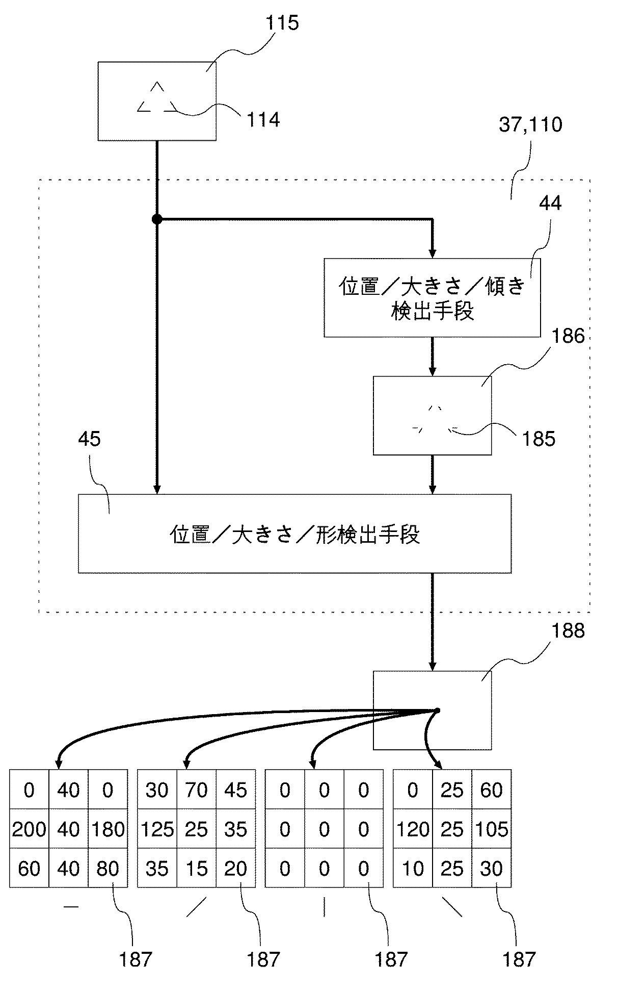
この他に、第5図に示すように、視覚装置2は、位置/大きさ/傾き検出手段44を用いて、画像記憶手段12によって記憶された少なくとも1つの物体領域141から傾き大きさ情報画像(inclination-size-information image)186を生成することにより、この物体領域141の位置、大きさ及び傾きを検出することができる。   In addition to this, as shown in FIG. 5, the visual device 2 uses the position / size / tilt detection means 44 to obtain the tilt magnitude information image from at least one object region 141 stored by the image storage means 12. By generating (inclination-size-information image) 186, the position, size, and inclination of the object region 141 can be detected.

そこで第6図に示すように、物体領域141を認識するための視覚装置2は、第3図及び 第4図 に示された複数の手段を組み合せた、パターン認識をするための視覚装置2に、第5図に示された 位置/大きさ/傾き検出手段44、複数の画像認識手段(image recognition means)29及び環境理解手段(environmental understanding means)31を組み合せたものである。これらの画像認識手段29の各々は、対応するパターンマッチング手段38から入力したマッチング結果画像147の各画素が表す、複数のテンプレート画像146とのマッチング結果を統合することにより、パターンマッチング手段38が入力した画像に対して1つの認識結果(recognition result)を求める。なお、マッチング結果を統合する方法として、誤差逆伝播法(バックプロパゲーション)によって学習する パーセプトロンなどのニューラルネットワークを用いることもできるが、一般には多数決のように単純にマッチング結果画像147のうち最も多いマッチング結果を選択することで十分である。環境理解手段31は、これらの認識結果及び 位置/大きさ/傾き検出手段44から入力された傾き大きさ情報画像186を用いて、物体領域141に対する 位置、大きさ、形、テクスチャ、色及び傾きを決定すると共に、 これらの情報から構成される環境データ(environmental datum)を生成する。さらに、この環境理解手段31は、デジタル画像111中の全ての物体の環境データを記憶することにより、これらの環境データのリストである環境地図(environmental map)を出力する。本発明が、デジタル画像111中の全ての物体に関して、事前に位置、大きさ、傾き、形及び色など如何なる情報を知らなくても、本発明は、デジタル画像111中の少なくとも1つの分離物体領域143が表す物体に対する環境地図を作成することができる。 したがって本発明の利用者は、事前に検出対象となる物体の情報を知らなくても、この利用者は本発明を容易に利用することができる。   Therefore, as shown in FIG. 6, the visual device 2 for recognizing the object region 141 is a visual device 2 for recognizing a pattern, which is a combination of a plurality of means shown in FIG. 3 and FIG. The position / size / tilt detection means 44, a plurality of image recognition means 29 and an environmental understanding means 31 shown in FIG. 5 are combined. Each of these image recognition means 29 integrates the matching results with a plurality of template images 146 represented by the respective pixels of the matching result image 147 input from the corresponding pattern matching means 38, so that the pattern matching means 38 inputs them. One recognition result is obtained for the obtained image. As a method for integrating the matching results, a neural network such as a perceptron that learns by the error back-propagation method (back propagation) can also be used. It is sufficient to select the matching result. The environment understanding unit 31 uses the recognition result and the tilt size information image 186 input from the position / size / tilt detection unit 44 to determine the position, size, shape, texture, color, and tilt with respect to the object region 141. At the same time, environmental data (environmental datum) composed of this information is generated. Further, the environment understanding means 31 stores environment data of all objects in the digital image 111, and outputs an environment map that is a list of these environment data. Even if the present invention does not know any information such as position, size, tilt, shape and color in advance for all objects in the digital image 111, the present invention can use at least one separated object region in the digital image 111. An environmental map for the object represented by 143 can be created. Therefore, even if the user of the present invention does not know the information of the object to be detected in advance, the user can easily use the present invention.

第7図に示すように、画像を理解するための視覚装置2は、物体領域141を認識するための視覚装置2で示された全ての手段に、図1の視覚装置2の実施形態で示された幾何解析手段37を加えたものである。この幾何解析手段37を加えたことにより、デジタル画像111中に複数の物体があったとしても、環境理解手段31はこれらの物体を容易に区別することができる。また、物体/背景分離手段16が物体領域141と背景領域を不完全に分離したとしても、この環境理解手段31は 幾何解析手段37が検出した物体の位置及び大きさと、位置/大きさ/傾き検出手段44が検出した物体領域141の位置、大きさと、を比較し、さらに幾何解析手段37が検出した物体の輪郭と、複数の画像認識手段29が決定した物体領域141が表す物体の種別及び色と、を比較することにより、この物体に対して適切な環境データを作成することができる。本発明が、デジタル画像111中の全ての物体に関して、事前に位置、大きさ、傾き、形及び色など如何なる情報を知らなくても、本発明は、デジタル画像111中の全ての物体に対する環境地図を作成することができる。したがって本発明の利用者は、事前に検出対象となる物体の情報を知らなくても、この利用者は本発明を容易に利用することができる。   As shown in FIG. 7, the visual device 2 for understanding the image is shown in the embodiment of the visual device 2 of FIG. 1 in all the means shown in the visual device 2 for recognizing the object area 141. The added geometric analysis means 37 is added. By adding this geometric analysis means 37, even if there are a plurality of objects in the digital image 111, the environment understanding means 31 can easily distinguish these objects. Even if the object / background separation means 16 incompletely separates the object area 141 and the background area, the environment understanding means 31 can detect the position and size of the object detected by the geometric analysis means 37 and the position / size / tilt. The position and size of the object area 141 detected by the detection means 44 are compared, and the contour of the object detected by the geometric analysis means 37 and the type of object represented by the object areas 141 determined by the plurality of image recognition means 29 and By comparing the colors, appropriate environmental data can be created for the object. Even if the present invention does not know any information such as position, size, inclination, shape, and color in advance for all objects in the digital image 111, the present invention can provide an environment map for all objects in the digital image 111. Can be created. Therefore, even if the user of the present invention does not know the information of the object to be detected in advance, the user can easily use the present invention.

第8図に示すように、物体を探索するための視覚装置2は、画像を理解するための視覚装置2で示された全ての手段に、画像取得手段(image capturing means)11、カメラ/環境座標変換手段(camera/environmental coordinate conversion means)20、2つの画像/環境座標変換手段(image/environmental coordinate conversion means)21、計時手段(timer means)32、物体位置推定手段(object position inference means)34、振動命令生成手段(vibration command generation means)25、運動制御手段(action control means)23及びカメラ命令生成手段(camera command generation means)26を加えたものである。画像取得手段11は、移動カメラ(moving camera)10が撮影した 動画像(animation image)を構成する複数のフレーム画像(frame images)の各々を順次デジタル画像111に変換する。もしこのフレーム画像がアナログ信号から構成されていれば、この画像取得手段11はフレーム画像をデジタル信号に変換し、このデジタル画像111を生成する。一方で、このフレーム画像がデジタル信号から構成される場合、もしこのデジタル信号が圧縮されていれば、この画像取得手段11はフレーム画像を伸張し、このデジタル画像111を生成する。さもなくば、この画像取得手段11はフレーム画像を直接このデジタル画像111に変換する。   As shown in FIG. 8, the visual device 2 for searching for an object includes an image capturing means 11, a camera / environment for all means shown in the visual device 2 for understanding an image. Camera / environmental coordinate conversion means 20, two image / environmental coordinate conversion means 21, timer means 32, object position inference means 34 A vibration command generation means 25, an action control means 23, and a camera command generation means 26 are added. The image acquisition means 11 sequentially converts each of a plurality of frame images constituting a moving image (animation image) taken by a moving camera 10 into a digital image 111. If the frame image is composed of an analog signal, the image acquisition unit 11 converts the frame image into a digital signal and generates the digital image 111. On the other hand, when the frame image is composed of a digital signal, if the digital signal is compressed, the image acquisition unit 11 expands the frame image and generates the digital image 111. Otherwise, the image acquisition means 11 directly converts the frame image into the digital image 111.

ところで、移動カメラ10はパン、チルト、ロール及びズームのうち、少なくとも1つを実行する場合、この移動カメラ10の向き、倍率及び傾きが変化するので、デジタル画像111が常に同じ倍率及び同じ傾きで同じ場所を表すとは限らない。したがって、幾何解析手段37及び位置/大きさ/傾き検出手段44が検出する物体の位置、大きさ及び傾きは、デジタル画像111毎に変化するかも知れない。そこで、その移動カメラ10がこの物体を 常時適切な大きさで撮影するために、視覚装置2は機能に応じて3つの座標系、つまりカメラ座標系(camera coordinate system)、画像座標系(image coordinate system)及び環境座標系(environmental coordinate system)を使い分ける。第一に、カメラ座標系は、文字通り移動カメラ10がパン、チルト及びズームを各々の最小制御単位で制御するために用いているカメラ内部の三次元球座標系である。一般にこのカメラ座標系の原点はホームポジションと呼ばれる、この移動カメラ10に固有の位置である。このカメラ座標系は物体の物理的位置を表すことができる唯一の座標系である。それにも関わらずこのカメラ座標系は移動カメラ10の機種毎に異なるため、このカメラ座標系には汎用性がない。そのため視覚装置2は他の手段から このカメラ座標系を秘匿する必要がある。第二に、画像座標系は、移動カメラ10によって撮影されたフレーム画像の中央、つまりレンズ光軸を原点とする、画素を単位とした二次元座標系である。これはフレーム画像中のどの画素に物体が位置するか表すために用いられる。したがってこの画像座標系はフレーム画像中にある複数の物体の細かな位置を区別するのには適しているが、この画像座標系だけではこれらの物体の物理的位置を 表すことができない。第三に、環境座標系は、視覚装置2が内部で物体の位置を論理的に統一して表すために用いている三次元球座標系である。この環境座標系は水平方向及び垂直方向にはラジアンを単位とした角度を用い、物体の大きさと物体までの距離の積を表すために、距離方向には1.0を単位とした実数を用いる。一般に物体の大きさが短時間で極端に変ることはないので、この物体までの距離と移動カメラ10の倍率は比例すると見做してよい。環境座標系の原点は任意である。つまり環境座標系は原則として環境座標系上の任意の2点の相対座標を表すために用いられる。視覚装置2は移動カメラ10によって撮影可能な環境中の物体を環境座標系に投射することで、複数の物体を区別することができる。   By the way, when the moving camera 10 executes at least one of pan, tilt, roll, and zoom, the direction, magnification, and inclination of the moving camera 10 change, so that the digital image 111 always has the same magnification and the same inclination. It does not necessarily represent the same place. Therefore, the position, size, and inclination of the object detected by the geometric analysis unit 37 and the position / size / tilt detection unit 44 may change for each digital image 111. Therefore, in order for the moving camera 10 to always photograph this object with an appropriate size, the visual device 2 has three coordinate systems, that is, a camera coordinate system and an image coordinate system according to the function. system) and environmental coordinate system. First, the camera coordinate system is literally a three-dimensional spherical coordinate system used by the moving camera 10 to control pan, tilt, and zoom in each minimum control unit. In general, the origin of the camera coordinate system is a position unique to the moving camera 10 called a home position. This camera coordinate system is the only coordinate system that can represent the physical position of an object. Nevertheless, since this camera coordinate system differs for each type of mobile camera 10, this camera coordinate system is not versatile. Therefore, the visual device 2 needs to conceal this camera coordinate system from other means. Second, the image coordinate system is a two-dimensional coordinate system in units of pixels with the center of the frame image taken by the moving camera 10, that is, the lens optical axis as the origin. This is used to represent at which pixel in the frame image the object is located. Therefore, this image coordinate system is suitable for distinguishing the fine positions of a plurality of objects in the frame image, but the physical position of these objects cannot be expressed only by this image coordinate system. Third, the environmental coordinate system is a three-dimensional spherical coordinate system that is used by the visual device 2 to logically unify and represent the position of an object inside. This environmental coordinate system uses angles in radians in the horizontal and vertical directions, and uses a real number in units of 1.0 in the distance direction to represent the product of the object size and the distance to the object. . In general, since the size of an object does not change extremely in a short time, it may be assumed that the distance to the object and the magnification of the moving camera 10 are proportional. The origin of the environmental coordinate system is arbitrary. That is, the environment coordinate system is used in principle to represent the relative coordinates of any two points on the environment coordinate system. The visual device 2 can distinguish a plurality of objects by projecting objects in the environment that can be photographed by the moving camera 10 onto the environment coordinate system.

そこでカメラ座標系及び画像座標系は各々環境座標系と相互に座標変換をする必要がある。その役割を果たしている手段がカメラ/環境座標変換手段20、画像/環境座標変換手段21及び運動制御手段23である。これらの手段は移動カメラ10及び画像取得手段11の仕様からカメラ座標系及び画像座標系の各単位を求め、環境座標系に変換するための行列を計算する。またカメラ座標系から環境座標系への変換行列の逆行列を計算することにより、環境座標系からカメラ座標系への変換行列も求めることができる。ただしカメラ座標系の原点が移動カメラ10のホームポジションであるので、カメラ座標系から変換された環境座標系の位置は環境座標系上の移動カメラ10のホームポジションからの相対位置となる。一方、環境座標系から変換されたカメラ座標系の位置はカメラ座標系上の移動カメラ10の現在位置からの相対位置となる。加えて、画像座標系は二次元座標系であるため、画像座標系のみでは環境座標系に変換することはできない。そのため画像/環境座標変換手段21では環境座標系で表された移動カメラ10の向き及び倍率と、フレーム画像中の物体の領域の大きさを用いて、随時変換行列を計算することにより、画像座標系から環境座標系に変換できるようにする。なお画像座標系から変換された環境座標系の位置は、画像の中心からの相対位置となる。   Therefore, the camera coordinate system and the image coordinate system need to be coordinate-transformed with the environmental coordinate system. Means that play the role are the camera / environment coordinate conversion means 20, the image / environment coordinate conversion means 21, and the motion control means 23. These means obtain each unit of the camera coordinate system and the image coordinate system from the specifications of the moving camera 10 and the image acquisition means 11, and calculate a matrix for conversion to the environment coordinate system. Further, by calculating the inverse matrix of the transformation matrix from the camera coordinate system to the environment coordinate system, the transformation matrix from the environment coordinate system to the camera coordinate system can also be obtained. However, since the origin of the camera coordinate system is the home position of the moving camera 10, the position of the environment coordinate system converted from the camera coordinate system is a relative position from the home position of the moving camera 10 on the environment coordinate system. On the other hand, the position of the camera coordinate system converted from the environment coordinate system is a relative position from the current position of the moving camera 10 on the camera coordinate system. In addition, since the image coordinate system is a two-dimensional coordinate system, the image coordinate system alone cannot be converted into the environment coordinate system. Therefore, the image / environment coordinate conversion means 21 calculates the image coordinates by calculating the conversion matrix as needed using the direction and magnification of the moving camera 10 expressed in the environment coordinate system and the size of the area of the object in the frame image. Enables conversion from the system to the environmental coordinate system. Note that the position of the environment coordinate system converted from the image coordinate system is a relative position from the center of the image.

ところが移動カメラ10が傾いていた場合、視覚装置2が環境座標系を上述のように求めることはできない。例えば第9図に示すように、形成エッジ情報画像115中の位置αに角度θ反時計回りに傾いた物体の形成エッジ情報114があるものとする。このときレンズ光軸に対応する形成エッジ情報画像115の中心οに対して 反時計回りに角度θ回転するように移動カメラ10を回転させると、エッジ情報形成手段15は回転後形成エッジ情報画像181を出力することができる。つまり回転後形成エッジ情報画像181中の位置αにおいて 物体は直立することになり、物体の種別の認識が容易になる。しかしながら回転後形成エッジ情報画像181中の位置αから求められた画像座標系の座標は、形成エッジ情報画像115中の位置αから求められた画像座標系の座標に比べて時計回りに角度θ回転した位置になる。そのため角度θが大きくなるか距離οαが長くなるに従って 両座標のずれが大きくなる。したがって回転後形成エッジ情報画像181中の位置αから回転前の画像座標系の座標を求めるためには、回転後形成エッジ情報画像181中の位置αを反時計回りに角度θ回転させた位置βを求めれば良い。なお、移動カメラ10の傾き及び角度θの単位はラジアンとする。   However, when the moving camera 10 is tilted, the visual device 2 cannot obtain the environmental coordinate system as described above. For example, as shown in FIG. 9, it is assumed that there is formation edge information 114 of an object inclined at an angle θ counterclockwise at a position α in the formation edge information image 115. At this time, when the moving camera 10 is rotated so as to rotate the angle θ counterclockwise with respect to the center ο of the formed edge information image 115 corresponding to the lens optical axis, the edge information forming means 15 causes the post-rotation formed edge information image 181. Can be output. That is, the object stands upright at the position α in the post-rotation formed edge information image 181, and the type of the object can be easily recognized. However, the coordinates of the image coordinate system obtained from the position α in the post-rotation formed edge information image 181 are rotated by an angle θ clockwise compared to the coordinates of the image coordinate system obtained from the position α in the formed edge information image 115. It will be in the position. Therefore, the deviation between both coordinates increases as the angle θ increases or the distance οα increases. Therefore, in order to obtain the coordinates of the image coordinate system before rotation from the position α in the post-rotation formed edge information image 181, the position β obtained by rotating the position α in the post-rotation formed edge information image 181 counterclockwise by the angle θ. Just ask. Note that the unit of the tilt and the angle θ of the mobile camera 10 is radians.

ここで回転後形成エッジ情報画像181中の位置αの画像座標を(α,α)とし、位置βの画像座標を(β,β)とすると、数式1に従って(α,α)から(β,β)を求めることができる。

Figure 0004589987
Here, when the image coordinates of the position α in the post-rotation formed edge information image 181 are (α x , α y ) and the image coordinates of the position β are (β x , β y ), (α x , α from y) (β x, β y ) can be obtained.
Figure 0004589987

これにより回転後形成エッジ情報画像181中の位置αから位置β、つまり形成エッジ情報画像115中の位置αを求めることができるので、結果として画像/環境座標変換手段21は回転後形成エッジ情報画像181中の位置αから正確に環境座標を求めることができる。   As a result, the position β in the formed edge information image 115 can be obtained from the position α in the formed edge information image 181 after rotation, that is, the position α in the formed edge information image 115 can be obtained. The environmental coordinates can be accurately obtained from the position α in 181.

上述を踏まえて、物体を探索するための視覚装置2では、カメラ/環境座標変換手段20が、移動カメラ10の向き及び倍率を、物理量に関係ない環境座標系の座標に変換する。なお、移動カメラ10の傾きは、ラジアンを単位とする角度に変換される。また、2つの画像/環境座標変換手段21は、傾き大きさ情報画像186の各画素及び形大きさ情報画像190の各画素を、それぞれこの環境座標系の座標に投射する。これにより、環境理解手段31は、環境座標系で表される環境データのリストである環境地図を生成することができる。また、この環境理解手段31は、計時手段32から1秒以下、一般には1ミリ秒を単位として、現在時刻を入力する。これにより、この環境理解手段31は、環境地図に含まれる各々の環境データにタイムスタンプを付けることができるので、この環境理解手段31は、1個の物体の軌跡を表すこともできるし、古くなった環境データを破棄することもできる。なお、この環境理解手段31は、カメラ/環境座標変換手段20から移動カメラ10の現在の向き、倍率及び傾きを入力することにより、この移動カメラ10の現在の向き、倍率及び傾きを環境データに変換する。この環境データは、外部のシステムが環境地図を利用する際に便利である。物体位置推定手段34は、環境地図が表す少なくとも1個の物体の中から1個を選び、この物体の軌跡から、この物体の現在位置及び傾きを推定する。この現在位置も環境座標系によって表される。振動命令生成手段25は、移動カメラ10を振動させるための命令を生成する。これにより、デジタル画像111も順次振動するので、動画像中で静止している物体があたかも移動しているようにエッジ情報生成手段14は見做すことができる。つまり、エッジ情報生成手段14は、この物体に対して粗エッジ情報112を生成することができる。なお、この物体がデジタル画像111中で、おおよそ2又は3画素程度で振動する場合に、エッジ情報生成手段14は、この物体だけから効率よく粗エッジ情報112を生成することができる。運動制御手段23は、物体位置推定手段34から物体の現在位置及び傾きを入力したか、又は振動命令生成手段25から移動カメラ10を振動させるための命令を入力した場合、この運動制御手段23は、移動カメラ10の移動先を決定し、カメラ座標系に変換する。カメラ命令生成手段26はこの移動先を入力して、移動カメラ10のパン、チルト、ロール及びズームのうち少なくとも1つを制御するための命令を生成する。本発明が、デジタル画像111中の全ての物体に関して、事前に位置、大きさ、傾き、形及び色など如何なる情報を知らなくても、本発明は、デジタル画像111中の全ての物体を探索することができる。したがって本発明の利用者は、事前に検出対象となる物体の情報を知らなくても、この利用者は本発明を容易に利用することができる。   Based on the above, in the visual device 2 for searching for an object, the camera / environment coordinate conversion means 20 converts the orientation and magnification of the moving camera 10 into coordinates in the environment coordinate system that are not related to physical quantities. Note that the tilt of the moving camera 10 is converted into an angle in radians. The two image / environment coordinate conversion means 21 projects each pixel of the inclination size information image 186 and each pixel of the shape size information image 190 to the coordinates of the environment coordinate system. As a result, the environment understanding unit 31 can generate an environment map that is a list of environment data represented in the environment coordinate system. The environment understanding means 31 inputs the current time from the time measuring means 32 in 1 second or less, generally in units of 1 millisecond. As a result, the environment understanding unit 31 can attach a time stamp to each environment data included in the environment map. Therefore, the environment understanding unit 31 can also represent the trajectory of one object, and can be old. It is also possible to discard the environmental data that has been lost. The environment understanding unit 31 inputs the current direction, magnification, and inclination of the moving camera 10 from the camera / environment coordinate conversion unit 20, and uses the current direction, magnification, and inclination of the moving camera 10 as environment data. Convert. This environmental data is convenient when an external system uses an environmental map. The object position estimating means 34 selects one from at least one object represented by the environment map, and estimates the current position and inclination of the object from the trajectory of the object. This current position is also represented by the environmental coordinate system. The vibration command generation means 25 generates a command for vibrating the mobile camera 10. As a result, the digital image 111 also vibrates sequentially, so that the edge information generating means 14 can be regarded as if a stationary object in the moving image is moving. That is, the edge information generation means 14 can generate the rough edge information 112 for this object. When this object vibrates in about 2 or 3 pixels in the digital image 111, the edge information generation unit 14 can efficiently generate the rough edge information 112 only from this object. When the motion control unit 23 inputs the current position and inclination of the object from the object position estimation unit 34 or receives a command for vibrating the mobile camera 10 from the vibration command generation unit 25, the motion control unit 23 Then, the movement destination of the moving camera 10 is determined and converted to the camera coordinate system. The camera command generation means 26 inputs this movement destination and generates a command for controlling at least one of pan, tilt, roll and zoom of the moving camera 10. The present invention searches for all objects in the digital image 111 without knowing any information such as position, size, tilt, shape and color in advance for all objects in the digital image 111. be able to. Therefore, even if the user of the present invention does not know the information of the object to be detected in advance, the user can easily use the present invention.

この他に、例えば第10図に示すように、物体の数を数えるための視覚装置2は、物体を探索するための視覚装置2で示された全ての手段に、この視覚装置2が生成した情報を出力するための2つの画像保持手段(image keeping means)39、2つ以上の認識結果保持手段(recognition-result keeping means)30、環境地図保持手段(environmental-map keeping means)33、物体計数手段(object counting means)35及び物体数保持手段(object number keeping means)36と、この視覚装置2が効率よく物体を探索するための色情報生成手段(color-information generation means)41、2つの位置/大きさ検出手段17、2つの画像/環境座標変換手段21及び2つの位置選択手段(position selection means)22と、外部から視覚装置2を制御するための制御命令入力手段(control command input means)24を有することもできる。   In addition to this, for example, as shown in FIG. 10, the visual device 2 for counting the number of objects is generated by the visual device 2 in all the means shown in the visual device 2 for searching for an object. Two image keeping means 39 for outputting information, two or more recognition-result keeping means 30, environmental-map keeping means 33, object counting An object counting means 35 and an object number keeping means 36, and a color-information generation means 41 and 2 positions for the visual device 2 to efficiently search for an object / Size detection means 17, two image / environment coordinate conversion means 21, two position selection means 22 and control command input means (control command i) for controlling the visual device 2 from the outside nput means) 24.

まず、1つの画像記憶手段12によって記憶されたデジタル画像111を外部のシステムが入力し終えるまで、1つの画像保持手段39はこのデジタル画像111を一定期間保持する。もう1つの画像記憶手段12によって記憶された物体領域画像142をこの外部のシステムが入力し終えるまで、もう1つの画像保持手段39はこの物体領域画像142を一定期間保持する。これら2つの画像を組み合せることにより、この外部のシステムはデジタル画像111から物体領域141に相当する領域を切り出すことができる。2つ以上の画像認識手段29によって決定された、分離物体領域143に対するパターン、テクスチャ及び色の認識結果を外部のシステムが入力し終えるまで、それぞれに対応する認識結果保持手段30はこれらの認識結果を一定期間保持する。なお、少なくとも1つの認識結果保持手段30が、パターンの認識結果及びテクスチャの認識結果を混在しながら出力することもある。環境理解手段31が生成する環境地図をこの外部のシステムが入力し終えるまで、環境地図保持手段33はこの環境地図を一定期間保持する。物体計数手段35は、この環境地図から一定時間内に検出された物体の個数を数え、物体数を出力する。この物体数をこの外部のシステムが入力し終えるまで、物体数保持手段36はこの物体数を一定期間保持する。   First, one image holding means 39 holds this digital image 111 for a certain period until the external system finishes inputting the digital image 111 stored by one image storage means 12. Another image holding means 39 holds the object area image 142 for a certain period until the external system finishes inputting the object area image 142 stored by the other image storage means 12. By combining these two images, this external system can cut out an area corresponding to the object area 141 from the digital image 111. Until the external system finishes inputting the pattern, texture, and color recognition results for the separated object region 143 determined by the two or more image recognition means 29, the recognition result holding means 30 corresponding to the recognition results holding means 30 respectively. Is held for a certain period. Note that at least one recognition result holding unit 30 may output a pattern recognition result and a texture recognition result in a mixed manner. The environment map holding means 33 holds this environment map for a certain period until the external system finishes inputting the environment map generated by the environment understanding means 31. The object counting means 35 counts the number of objects detected within a predetermined time from the environment map and outputs the number of objects. Until this external system finishes inputting this number of objects, the object number holding means 36 holds this number of objects for a certain period.

次に、色情報生成手段41は、デジタル画像111の各画素から赤色、黄色及び白色のような特定の色を表す画素を選び、色情報画像172を生成する。この色情報画像172は、明るさが常に変化し、無数の色が溢れる実世界において物体を認識する場合にはあまり役に立たないが、血液、炎、信号機、道路標識及びヘッドライトの光など、注意を必要としたり、危険を及ぼす可能性がある物体を急いで探索する場合には極めて有効である。1つの位置/大きさ検出手段17は、この色情報画像172から、注意が必要である少なくとも1個の物体の位置及び大きさを検出し、重複情報画像132を生成する。1つの画像/環境座標変換手段21は、この重複情報画像132の各画素を構成する重複情報131を環境座標系に投射する。1つの位置選択手段22は、全ての重複情報131から1つを選択する。一方で、もう1つの位置/大きさ検出手段17は、粗エッジ情報画像113から、少なくとも1個の移動物体の位置及び大きさを検出し、重複情報画像132を生成する。もう1つの画像/環境座標変換手段21は、この重複情報画像132の各画素を構成する重複情報131を環境座標系に投射する。もう1つの位置選択手段22は、全ての重複情報131から1つを選択する。また、制御命令入力手段24は、外部から利用者及び適当なシステムが指示した制御命令を入力する。そこで運動制御手段23は、環境地図によって表された物体以外にも、移動カメラ10の周辺にある物体及びこの利用者及びこのシステムが指示した物体の中から1つを選び、選ばれた物体の環境座標をカメラ命令生成手段26に伝える。   Next, the color information generation unit 41 selects a pixel representing a specific color such as red, yellow, and white from each pixel of the digital image 111 and generates a color information image 172. This color information image 172 is not very useful when recognizing objects in the real world where the brightness is constantly changing and countless colors overflow, but attention is paid to blood, flames, traffic lights, road signs and headlights, etc. It is extremely effective when searching for an object that may require danger or may cause danger. One position / size detection unit 17 detects the position and size of at least one object that requires attention from the color information image 172, and generates a duplicate information image 132. One image / environment coordinate conversion means 21 projects overlap information 131 constituting each pixel of the overlap information image 132 onto the environment coordinate system. One position selection unit 22 selects one from all the duplication information 131. On the other hand, the other position / size detection means 17 detects the position and size of at least one moving object from the rough edge information image 113 and generates an overlapping information image 132. Another image / environment coordinate conversion means 21 projects the overlap information 131 constituting each pixel of the overlap information image 132 onto the environment coordinate system. Another position selection means 22 selects one from all the duplication information 131. The control command input means 24 inputs a control command instructed by the user and an appropriate system from the outside. Therefore, the motion control means 23 selects one of the objects in the vicinity of the mobile camera 10 and the objects designated by the user and the system other than the objects represented by the environment map, and selects the selected object. The environmental coordinates are transmitted to the camera command generation means 26.

これにより、本発明が、デジタル画像111中の全ての物体に関して、事前に位置、大きさ、傾き、形及び色など如何なる情報を知らなくても、本発明は、デジタル画像111中の全ての物体を探索し、物体の個数を数えることができる。したがって本発明の利用者は、事前に検出対象となる物体の情報を知らなくても、この利用者は本発明を容易に利用することができる。なお、実際の利用に際しては、この利用者は第10図の中から必要な手段だけを選ぶことができるし、さらに他の手段を追加することもできる。   Thus, the present invention can detect all objects in the digital image 111 without knowing any information such as position, size, tilt, shape and color in advance. And the number of objects can be counted. Therefore, even if the user of the present invention does not know the information of the object to be detected in advance, the user can easily use the present invention. In actual use, the user can select only necessary means from FIG. 10, and can add other means.

さて、視覚装置2で用いられている画像記憶手段12、色情報生成手段41、エッジ情報生成手段14、エッジ情報形成手段15、位置/大きさ検出手段17、位置/大きさ/傾き検出手段44、幾何解析手段37、物体/背景分離手段16、領域正規化手段27、マスク手段40、画像保持手段39、及びパターンマッチング手段38は、配列演算ユニット100から構成されるデータ処理装置110を用いることにより実装することができる。そこで以下では、配列演算ユニット100を利用したデータ処理装置110の実施形態を挙げ、この視覚装置2を図面を参照して説明する。   Now, the image storage means 12, the color information generation means 41, the edge information generation means 14, the edge information formation means 15, the position / size detection means 17, and the position / size / tilt detection means 44 used in the visual device 2. The geometric processing unit 37, the object / background separation unit 16, the region normalization unit 27, the mask unit 40, the image holding unit 39, and the pattern matching unit 38 use the data processing device 110 configured by the array operation unit 100. Can be implemented. Therefore, in the following, an embodiment of the data processing device 110 using the array operation unit 100 will be described, and the visual device 2 will be described with reference to the drawings.

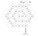
まず配列演算ユニット100は、入力画像の1つの画素とその近傍画素を用いることにより、出力画像の1つの画素を生成する。そこで第11図に示したように、配列演算ユニット100を入力画像のサイズに合わせて格子状に配列したデータ処理装置110を用いることにより、データ処理装置110は入力画像から出力画像を生成することができる。なお第11図において、配列演算ユニット100をAOUと略記する。また第11図では、配列演算ユニット100は正方格子状に配列されているが、勿論実装面積を最小にするために、配列演算ユニット100を六角格子状、つまり最密充填構造に配置しても良い。この場合、配列演算ユニット100間の複数の信号線の一部はジグザグに配線される。次に配列演算ユニット100は専用ハードウェアによって実装されても良いし、汎用コンピュータ上でソフトウェアによって実装することもできる。つまり入力画像から出力画像を生成することができれば、実装手段は制限されない。したがって配列演算ユニット100のアルゴリズムを示すことにより、データ処理装置110の画像処理を示すことができる。そこで配列演算ユニット100のアルゴリズムを示すために、第10図で示された画像記憶手段12、色情報生成手段41、エッジ情報生成手段14、エッジ情報形成手段15、位置/大きさ検出手段17、位置/大きさ/傾き検出手段44、幾何解析手段37、領域正規化手段27、マスク手段40、画像保持手段39、及びパターンマッチング手段38で用いる数式について説明する。   First, the array operation unit 100 generates one pixel of the output image by using one pixel of the input image and its neighboring pixels. Therefore, as shown in FIG. 11, by using the data processing device 110 in which the array operation units 100 are arranged in a grid according to the size of the input image, the data processing device 110 generates an output image from the input image. Can do. In FIG. 11, the array operation unit 100 is abbreviated as AOU. In FIG. 11, the array operation units 100 are arranged in a square lattice shape. However, in order to minimize the mounting area, the array operation units 100 may be arranged in a hexagonal lattice shape, that is, in a close-packed structure. good. In this case, some of the plurality of signal lines between the array operation units 100 are wired in a zigzag manner. Next, the array operation unit 100 may be implemented by dedicated hardware, or may be implemented by software on a general-purpose computer. That is, if the output image can be generated from the input image, the mounting means is not limited. Therefore, the image processing of the data processing device 110 can be shown by showing the algorithm of the array operation unit 100. Therefore, in order to show the algorithm of the array operation unit 100, the image storage means 12, the color information generation means 41, the edge information generation means 14, the edge information formation means 15, the position / size detection means 17, shown in FIG. Formulas used in the position / size / tilt detection unit 44, the geometric analysis unit 37, the region normalization unit 27, the mask unit 40, the image holding unit 39, and the pattern matching unit 38 will be described.

幅w、高さh、帯域数bの任意の2階調画像をx、y、wとすると、x、y、wは各々位置p(i,j,k)の 帯域画値xijk、yijk、wijkをy用いて数式2、3及び4のように表される。なお太字はベクトルを示す。またnは非負の整数、w、h、b、i、j、kは自然数である。

Figure 0004589987
Assuming that an arbitrary 2 n gradation image having a width w, a height h, and the number of bands b is x, y, and w, x, y, and w are band image values x ijk at a position p (i, j, k), respectively. y ijk and w ijk are expressed as Equations 2, 3, and 4 using y. Bold indicates a vector. N is a non-negative integer, and w, h, b, i, j, and k are natural numbers.
Figure 0004589987

まず前記画像の各帯域画素値に対する点処理に関する関数について以下で説明する。
画像xを二値画像に変換する場合、数式5に従って帯域画素値を二値化する。

Figure 0004589987
First, a function related to point processing for each band pixel value of the image will be described below.
When the image x is converted into a binary image, the band pixel value is binarized according to Equation 5.
Figure 0004589987

画像xを帯域最大値画像に変換する場合、数式6に従ってi行j列の画素の各帯域の値のうち最大値を選択する。なお前記帯域最大値画像は単帯域画像となるので、便宜上帯域数1の前記画像として取り扱うことにする。したがって関数Bij1(x)の第3添字は1となっている。

Figure 0004589987
When the image x is converted into a band maximum value image, the maximum value is selected from the values of the respective bands of the pixels in i rows and j columns according to Equation 6. Since the band maximum value image is a single band image, it is handled as the image having the band number 1 for convenience. Therefore, the third subscript of the function B ij1 (x) is 1.
Figure 0004589987

画像xが二値画像であるとして、画像xを反転させる場合、数式7に従って計算する。

Figure 0004589987
When the image x is inverted assuming that the image x is a binary image, the calculation is performed according to Equation 7.
Figure 0004589987

画像xの位置p(i,j,k)における対数変換は数式8に従って行われる。ここでeはオフセットであり、自然対数関数が出力する値が有効範囲に入るようにするために使われるので、一般にe=1で十分である。この対数化により帯域画素値同士の除算を減算にすることができる。また画像xが2階調のデジタル画像111であるとすると、帯域数に関わらず2個の要素を含むルックアップテーブルをメモリ102上に持つならば、毎回自然対数関数を計算する必要もなく、標準的な対数表を持つ必要もなくなる。

Figure 0004589987
Logarithmic transformation at the position p (i, j, k) of the image x is performed according to Equation 8. Here, e is an offset, and is used to make the value output by the natural logarithmic function fall within the valid range, so that e = 1 is generally sufficient. This logarithmization can subtract the division between band pixel values. If the image x is a digital image 111 having 2n gradations, a natural logarithmic function needs to be calculated every time if the memory 102 has a lookup table including 2n elements regardless of the number of bands. There is no need to have a standard logarithmic table.
Figure 0004589987

さて、画像の位置p(i,j,k)におけるq近傍の位置の集合Pijk(q)は数式9によって表される。ただしqは4、8、24、48、80、120、(2r+1)−1と続く数列であり、rは自然数である。なお画像サイズをはみ出した位置が集合Pijk(q)に含まれる場合には、特に指定がない限り位置p(i,j,k)を代用するものとする。またこれ以外のときは、指定に従い、画素値が0に相当し、しかも画像に含まれない架空の位置を代用する。これにより辺縁処理は自動的に行われる。したがって集合Pijk(q)の要素の数Nijkは常にqとなる。

Figure 0004589987
Now, a set P ijk (q) of positions in the vicinity of q at the position p (i, j, k) of the image is expressed by Equation 9. However, q is a sequence of 4, 8, 24, 48, 80, 120, (2r + 1) 2 -1, and r is a natural number. If the position where the image size protrudes is included in the set P ijk (q), the position p (i, j, k) is substituted unless otherwise specified. In other cases, according to the designation, an imaginary position whose pixel value corresponds to 0 and is not included in the image is substituted. Thereby, the edge processing is automatically performed. Therefore, the number N ijk of elements of the set P ijk (q) is always q.
Figure 0004589987

そこで次に画像の各帯域画素値に対する最大8近傍182の近傍処理に関する関数及びオペレータについて以下で説明する。
画像xの位置p(i,j,k)における平滑化は数式10に従って行われる。ただしint(v)は実数vの小数点以下切り捨てを意味するものとする。もし画像xの帯域画素値が整数値であるならば、ハードウェアの実装時にNijk=4のときxlmkの総和に対して右シフト命令を2回、Nijk=8のときxlmkの総和に対して右シフト命令を3回実行するような回路に変更することにより、除算を実行する回路を省くことができる。

Figure 0004589987
Therefore, a function and an operator relating to the neighborhood processing of the maximum 8 neighborhoods 182 for each band pixel value of the image will be described below.
Smoothing at the position p (i, j, k) of the image x is performed according to Equation 10. However, int (v) means that the decimal part of the real number v is rounded down. If If a band-pixel value of the image x is an integer value, twice the right shift instruction based on the sum of x LMK when N ijk = 4 in hardware implementation, the sum of x LMK when N ijk = 8 On the other hand, by changing to a circuit that executes the right shift instruction three times, a circuit that executes division can be omitted.
Figure 0004589987

ラプラシアンの計算であるが、これは数式11に示すように単なる2階差分オペレータである。8近傍182の方がノイズの微妙な変化を捉えてゼロ点およびゼロ交差が多くなり、本発明には向いている。ただしNijkが4か8であるので、もしハードウェアの実装時にNijk=4のときxijkに対して左シフト命令を2回、Nijk=8のときxijkに対して左シフト命令を3回実行するような回路に変更することにより、実数の乗算を実行する回路を省くことができる。

Figure 0004589987
This is a Laplacian calculation, which is simply a second-order difference operator as shown in Equation 11. The 8-neighbor 182 is more suitable for the present invention because it captures subtle changes in noise and has more zero points and zero crossings. However, since N ijk is 4 or 8, if two left shift instruction to the x ijk when N ijk = 4 in hardware implementation, the left shift instruction to the x ijk when N ijk = 8 By changing to a circuit that executes three times, a circuit that performs real multiplication can be omitted.
Figure 0004589987

ラプラシアンによって求められた値からゼロ点を見付ける方法として、従来は正から負に変化する画素を見付けていたが、本発明では数式12に従い、負から正にゼロ交差する画素の他に、負からゼロやゼロから正などゼロ点が経由したり、ゼロが継続する画素を見付けるようにする。本発明では、数式12が見付けたゼロ点はエッジがある場所ではなく、ノイズがある場所、つまりエッジがない場所になる。また数式12により実数値の二値化も同時に行っている。

Figure 0004589987
As a method of finding the zero point from the value obtained by the Laplacian, conventionally, a pixel that changes from positive to negative has been found. However, according to the present invention, in addition to a pixel that crosses zero from negative to positive, the pixel from negative to positive is obtained. Find a pixel that passes through zero points such as zero or positive from zero or continues zero. In the present invention, the zero point found by Equation 12 is not a place where there is an edge, but a place where there is noise, that is, a place where there is no edge. In addition, real value binarization is also performed simultaneously using Equation 12.
Figure 0004589987

画像xが任意の二値画像であるとして、画像xのうち孔が空いている画素を埋める場合には、数式13に従い計算するここでfは埋めるべき孔の大きさを表すパラメータであり、一般にはf=1で十分である。なお4近傍の場合にはその性質上対角線を検知することができないので、極力8近傍182にした方がよい。

Figure 0004589987
Assuming that the image x is an arbitrary binary image, when filling a pixel with a hole in the image x, calculation is performed according to Equation 13, where f is a parameter indicating the size of the hole to be filled. F = 1 is sufficient. In the case of 4 neighborhoods, a diagonal line cannot be detected due to its nature, so it is better to use 8 neighborhoods 182 as much as possible.
Figure 0004589987

画像xが任意の二値画像であるとして、画像xのうち孤立点ないし孤立孔を削除する場合には、数式14に従い計算する。なお4近傍の場合にはその性質上対角線を検知することができないので、極力8近傍182にした方がよい。

Figure 0004589987
Assuming that the image x is an arbitrary binary image, when an isolated point or an isolated hole is deleted from the image x, the calculation is performed according to Equation 14. In the case of 4 neighborhoods, a diagonal line cannot be detected due to its nature, so it is better to use 8 neighborhoods 182 as much as possible.
Figure 0004589987

画像xが任意の二値画像であるとして、画像xのうち線幅が1である画素を検知するために、4近傍画素を用いて数式15に従い計算する。

Figure 0004589987
Assuming that the image x is an arbitrary binary image, calculation is performed according to Equation 15 using four neighboring pixels in order to detect a pixel having a line width of 1 in the image x.
Figure 0004589987

2つの画像x、yが任意の二値画像であり、画像yが画像xのうち線幅が1である画素を検知した画像であるとすると、画像xのうち線幅が1である画素の線幅を拡張するために、4近傍画素を用いて数式16に従い計算する。

Figure 0004589987
Assuming that two images x and y are arbitrary binary images, and the image y is an image in which a pixel having a line width of 1 in the image x is detected, a pixel having a line width of 1 in the image x. In order to extend the line width, calculation is performed according to Equation 16 using 4 neighboring pixels.
Figure 0004589987

そこで数式15の線幅検知と数式16の線幅拡張を用いると、数式17に従い二値画像の線幅補完を簡単に記述することができる。

Figure 0004589987
Therefore, using the line width detection of Expression 15 and the line width extension of Expression 16, the line width complementation of the binary image can be simply described according to Expression 17.
Figure 0004589987

次に画像の各帯域画素値に対する近傍処理に関する関数及びオペレータについて以下で説明する。
2つの画像x、yがある場合、これらの画像の最大値画像は数式18に従って計算される。

Figure 0004589987
Next, functions and operators related to the neighborhood processing for each band pixel value of the image will be described below.
When there are two images x and y, the maximum image of these images is calculated according to Equation 18.
Figure 0004589987

2つの画像x、yがある場合、これらの画像の差分は数式19に従って計算される。

Figure 0004589987
When there are two images x and y, the difference between these images is calculated according to Equation 19.
Figure 0004589987

ここで数式11のラプラシアンと数式19の差分を用いると、数式20に従い画像の鮮鋭化を簡単に記述することができる。

Figure 0004589987
Here, if the difference between the Laplacian of Equation 11 and Equation 19 is used, the sharpening of the image can be simply described according to Equation 20.
Figure 0004589987

2つの画像x、yがあり、画像yが単帯域二値画像である場合、数式21に従い、画像yの帯域画素値を用いて画像xの各帯域画素値を抜き出すことができる。

Figure 0004589987
When there are two images x and y and the image y is a single-band binary image, each band pixel value of the image x can be extracted using the band pixel value of the image y according to Equation 21.
Figure 0004589987

2つの画像x、yがあり、画像xとyが二値画像である場合、数式22に従い、画像xを基に 画像yを整形することができる。

Figure 0004589987
If there are two images x and y, and the images x and y are binary images, the image y can be shaped based on the image x according to Equation 22.
Figure 0004589987

2つの画像x、yがあり、画像yが二値画像である場合、数式23に従い、画像yで指定されなかった画像xの帯域画素値を、画像xの帯域画素値の近傍のうち画像yで指定された画像xの帯域画素値の平均値で補間する。ただしint(v)は実数vの小数点以下切り捨てを意味するものとする。なお画像yが二値画像であるため分母は正数となるので、メモリ102に1からqまでの逆数を記憶させることにより、整数の除算を実数の乗算に置き換えることができる。

Figure 0004589987
When there are two images x and y, and the image y is a binary image, the band pixel value of the image x not specified in the image y is calculated from the neighborhood of the band pixel value of the image x according to Equation 23. Is interpolated with the average value of the band pixel values of the image x specified in (1). However, int (v) means that the decimal part of the real number v is rounded down. Since the image y is a binary image, the denominator is a positive number. By storing the reciprocal from 1 to q in the memory 102, integer division can be replaced with real multiplication.
Figure 0004589987

さて本発明では、画素の位置や移動量なども画像データのように扱うことで処理を単純にしている。これを位置の画像化と呼ぶ。以下では位置の画像化に関する幾つかの関数及びオペレータについて説明する。
まず位置p(l,m,o)のl、m、o各々の値を画像データとして帯域画素値に変換するオペレータを#とし、変換された帯域画素値を#p(l,m,o)とする。次に帯域画素値が位置p(i,j,k)から位置p(i+l,j+m,k+o)へ移動する場合を考える。 このとき帯域画素値の移動量は位置p(l,m,o)として表されるものとする。つまり移動量はある位置からのベクトルと見做すことができる。最後に帯域画素値から位置を取り出すオペレータを#−1とする。したがって#−1#p(l,m,o)=p(l,m,o)となる。
In the present invention, the processing is simplified by treating the pixel position, the movement amount, and the like like image data. This is called position imaging. The following describes some functions and operators related to position imaging.
First, an operator that converts each of l, m, and o values at position p (l, m, o) into band pixel values as image data is #, and the converted band pixel values are #p (l, m, o). And Next, consider a case where the band pixel value moves from the position p (i, j, k) to the position p (i + l, j + m, k + o). At this time, the movement amount of the band pixel value is expressed as a position p (l, m, o). That is, the movement amount can be regarded as a vector from a certain position. Finally, an operator that extracts a position from the band pixel value is set to # -1 . Therefore, # -1 #p (l, m, o) = p (l, m, o).

そこで数式24に従い、移動量p(i,j,k)を幅方向と高さ方向で表される平面内で180度反対方向に向けることができる。

Figure 0004589987
Therefore, according to Expression 24, the movement amount p (i, j, k) can be directed in the opposite direction by 180 degrees in the plane represented by the width direction and the height direction.
Figure 0004589987

画像xがあり、画像xが単帯域二値画像である場合、画像xの位置p(i,j,1)における 重心位置への移動量は数式25に従い計算される。なお、本来重心を計算する際には除算を行う必要があるが、8近傍182内への移動量を計算する際に除算は相殺されてしまうので、数式25では除算が省かれている。

Figure 0004589987
When there is an image x and the image x is a single-band binary image, the amount of movement of the image x to the center of gravity position at the position p (i, j, 1) is calculated according to Equation 25. In addition, although it is originally necessary to perform division when calculating the center of gravity, since division is canceled when calculating the amount of movement into the 8-neighbor 182, division is omitted in Equation 25.
Figure 0004589987

移動量p(i,j,k)から、数式26、27及び28に従い8近傍182内への移動量を計算し、移動量画像に画像化することができる。なお数式27及び28は、画像の離散化により数式26では対応しきれない場合にのみ利用する。

Figure 0004589987
Figure 0004589987
From the movement amount p (i, j, k), the movement amount into the eight neighborhood 182 can be calculated according to the mathematical expressions 26, 27, and 28, and imaged into a movement amount image. The equations 27 and 28 are used only when the image 26 cannot be handled due to image discretization.
Figure 0004589987
Figure 0004589987

したがって数式25、26、27及び28を用いると、数式29、30及び31に従い、単帯域二値画像xの重心方向への移動量画像の帯域画素値を簡単に記述することができる。なお移動量画像の帯域数は1となる。

Figure 0004589987
Therefore, when Expressions 25, 26, 27, and 28 are used, the band pixel value of the movement amount image in the center of gravity direction of the single-band binary image x can be simply described according to Expressions 29, 30, and 31. Note that the number of bands of the movement amount image is 1.
Figure 0004589987

一方で数式24を用いると重心位置の反対位置を求めることができるので、数式32に従い、単帯域二値画像xの重心と反対方向への移動量画像の帯域画素値を簡単に記述することができる。なお移動量画像の帯域数は1となる。

Figure 0004589987
On the other hand, since the position opposite to the center of gravity position can be obtained using Expression 24, the band pixel value of the movement amount image in the direction opposite to the center of gravity of the single-band binary image x can be simply described according to Expression 32. it can. Note that the number of bands of the movement amount image is 1.
Figure 0004589987

2つの画像x、yがあり、画像yが移動量画像である場合、数式33に従い、画像yで指し示された移動位置に画像xの帯域画素値を移動した後、同じ帯域画素に移動した帯域画素値の合計を濃淡画像にすることができる。

Figure 0004589987
When there are two images x and y and the image y is a movement amount image, the band pixel value of the image x is moved to the movement position indicated by the image y according to Equation 33 and then moved to the same band pixel. The sum of the band pixel values can be a gray image.
Figure 0004589987

そこで数式5、29、30、31及び33を用いることにより、数式34、数式35及び数式36に従い、単帯域濃淡画像xを近傍の重心方向に移動した後、同じ帯域画素に移動した帯域画素値の合計を簡単に記述することができる。

Figure 0004589987
Therefore, by using Equations 5, 29, 30, 31, and 33, the band pixel value that has moved to the same band pixel after moving the single band grayscale image x in the vicinity of the center of gravity in accordance with Equation 34, Equation 35, and Equation 36. Can be described easily.
Figure 0004589987

ところで、数式33において近傍数qが8に限定されると、移動量画像yは画素毎に8近傍182の中から移動元を特定することができる。そこで、画像xが重複情報画像132であり、しかも第12図に示すように、xの各画素の8近傍182に対して反時計回りに1から8までの番号が付けられた場合、数式37から数式44までの8つの数式は、それぞれ8個の移動元毎に、移動可能な画像xの帯域画素値を求めることができる。

Figure 0004589987
Figure 0004589987
By the way, if the number of neighbors q is limited to 8 in Expression 33, the movement amount image y can specify the movement source from among the eight neighbors 182 for each pixel. Therefore, when the image x is the duplication information image 132 and, as shown in FIG. 12, the numbers from 1 to 8 are assigned counterclockwise to the 8-neighbor 182 of each pixel of x, Expression 37 Eq. 8 to Eq. 44 can determine the band pixel value of the movable image x for each of the eight movement sources.
Figure 0004589987
Figure 0004589987

そこで数式34、35及び36の代りに数式45、46及び47を用いることにより、8個の移動元重複情報183から構成される8帯域濃淡画像x、及び重複情報131から構成される単帯域濃淡画像yから、8個の移動元毎の移動元重複情報183が生成される。

Figure 0004589987
なお、条件によっては、Γ ijk(Φ(y),Δ(Φ(y))) の代りに、Γ ijk(y,Δ(Φ(y)))を用いることもできる。 Therefore, by using the mathematical expressions 45, 46 and 47 instead of the mathematical expressions 34, 35 and 36, the eight-band gray image x composed of the eight movement source duplication information 183 and the single-band gray image composed of the duplication information 131. From the image y, the movement source duplication information 183 for each of the eight movement sources is generated.
Figure 0004589987
Depending on the conditions, gamma * ijk instead of (Φ (y), Δ ( Φ (y))), Γ * ijk (y, Δ (Φ (y))) can also be used.

2つの画像x、yがあり、画像xが二値画像で、画像yが移動量画像である場合、画像xの各帯域画素値の移動先の位置を 求めることができるので、移動先が重複する帯域画素値を見つけることができる。そこで画像xの各帯域画素値の移動先が重複することなく、しかも移動する各帯域画素値が存在することを表す移動可能画像の帯域画素値は、数式48に従い生成される。なお移動可能画像の帯域数は1となる。

Figure 0004589987
When there are two images x and y, the image x is a binary image, and the image y is a movement amount image, the movement destination position of each band pixel value of the image x can be obtained, so the movement destinations overlap. The band pixel value to be found can be found. Therefore, the band pixel value of the movable image indicating that each band pixel value to be moved is present without overlapping the movement destination of each band pixel value of the image x is generated according to Equation 48. The number of bands of movable images is 1.
Figure 0004589987

3つの画像x、y、wがあり、画像yが移動可能画像であり、画像wが移動量画像である場合、数式49に従い画像xの帯域画素値を移動することができる。

Figure 0004589987
When there are three images x, y, and w, the image y is a movable image, and the image w is a movement amount image, the band pixel value of the image x can be moved according to Equation 49.
Figure 0004589987

そこで数式32、数式48及び数式49を用いると、数式50に従い、二値画像yから計算される重心位置と反対方向に画像xの帯域画素を移動することで得られる画像の帯域画素値を簡単に記述することができる。

Figure 0004589987
Therefore, using Equation 32, Equation 48, and Equation 49, according to Equation 50, the band pixel value of the image obtained by moving the band pixel of the image x in the direction opposite to the centroid position calculated from the binary image y can be easily obtained. Can be described in
Figure 0004589987

そこで数式2から数式50までを用いることにより、第10図で示された画像記憶手段12、色情報生成手段41、エッジ情報生成手段14、エッジ情報形成手段15、位置/大きさ検出手段17、位置/大きさ/傾き検出手段44、領域正規化手段27、マスク手段40、及び画像保持手段39 を実装するデータ処理装置110の全ての配列演算ユニット100のアルゴリズムを記述することができる。以下では、データ処理装置110中の任意の配列演算ユニット100のアルゴリズムを用いて、画像記憶手段12、色情報生成手段41、エッジ情報生成手段14、エッジ情報形成手段15、 位置/大きさ検出手段17、位置/大きさ/傾き検出手段44、領域正規化手段27、マスク手段40、及び画像保持手段39を説明する。   Therefore, by using Expressions 2 to 50, the image storage means 12, the color information generation means 41, the edge information generation means 14, the edge information formation means 15, the position / size detection means 17 shown in FIG. The algorithm of all the array operation units 100 of the data processing apparatus 110 that implements the position / size / tilt detection means 44, the area normalization means 27, the mask means 40, and the image holding means 39 can be described. In the following, the image storage means 12, the color information generation means 41, the edge information generation means 14, the edge information formation means 15, the position / size detection means, using the algorithm of an arbitrary array operation unit 100 in the data processing device 110. 17, position / size / tilt detection means 44, area normalization means 27, mask means 40, and image holding means 39 will be described.

データ処理装置110によって実現される画像記憶手段12がデジタル画像111を記憶するために、格子状に配列された配列演算ユニット100は同期して並列に動作する。格子上i行j列に配置された配列演算ユニット100をAOUijとすると、AOUijのアルゴリズムは第13図のようになる。 In order for the image storage means 12 realized by the data processing device 110 to store the digital image 111, the array operation units 100 arranged in a lattice form operate in parallel in synchronization. When the lattice i and a row j array operation unit 100 at a column and AOU ij, Algorithm of AOU ij is shown in FIG. 13.

ステップ1201で、AOUijを格子上のi行j列に配置する。これは論理的であれ物理的であれ、AOUijの近傍を決定するために必要である。
ステップ1202で、AOUijの近傍や変数の初期値を設定する。
ステップ1203で、順次入力されるデジタル画像111が無くなったかどうか判断する。もしデジタル画像111が無ければ(ステップ1203:YES)、アルゴリズムを終了する。もしデジタル画像111があれば(ステップ1203:NO)、ステップ1204に移行する。ただし特定の画像サイズのみに対して配列演算ユニット100を実装する場合には、無限ループにしても良い。
In step 1201, AOU ij is arranged in i rows and j columns on the grid. This is necessary to determine the neighborhood of AOU ij , whether logical or physical.
In step 1202, the vicinity of AOU ij and initial values of variables are set.
In step 1203, it is determined whether or not the sequentially input digital images 111 are lost. If there is no digital image 111 (step 1203: YES), the algorithm is terminated. If there is a digital image 111 (step 1203: NO), the process proceeds to step 1204. However, when the array operation unit 100 is mounted only for a specific image size, an infinite loop may be used.

ステップ1204で、デジタル画像111が準備されるまで入力待ちをする。
ステップ1205で、 デジタル画像111のi行j列の画素を帯域数分入力する。このためAOUijは少なくとも帯域数分の画像データを記憶するメモリ102を必要とする。
ステップ1206で、入力待ちの間、出力できるように、デジタル画像111のi行j列の画素を記憶する。
ステップ1207で、デジタル画像111の帯域画素値を出力する。その後ステップ1203に戻る。
これにより、配列演算ユニット100から構成されるデータ処理装置110を用いて、画像記憶手段12はデジタル画像111を記憶することができる。
In step 1204, input is waited until the digital image 111 is prepared.
In step 1205, the pixels of i rows and j columns of the digital image 111 are inputted by the number of bands. For this reason, AOU ij requires a memory 102 for storing image data for at least the number of bands.
In step 1206, the pixels of i rows and j columns of the digital image 111 are stored so that they can be output while waiting for input.
In step 1207, the band pixel value of the digital image 111 is output. Thereafter, the process returns to step 1203.
Thus, the image storage unit 12 can store the digital image 111 using the data processing device 110 configured by the array operation unit 100.

第14図に示すように、データ処理装置110によって実現される色情報生成手段41がデジタル画像111の各画素から色情報171を生成するために、格子状に配列された配列演算ユニット100は同期して並列に動作する。格子上i行j列に配置された 配列演算ユニット100をAOUijとすると、AOUijのアルゴリズムは第15図のようになる。 As shown in FIG. 14, in order for the color information generating means 41 realized by the data processing device 110 to generate color information 171 from each pixel of the digital image 111, the array operation units 100 arranged in a grid are synchronized. And work in parallel. When the lattice i and a row j array operation unit 100 at a column and AOU ij, Algorithm of AOU ij is shown in Figure 15.

ステップ4101で、AOUijを格子上のi行j列に配置する。これは論理的であれ物理的であれ、AOUijの近傍を決定するために必要である。
ステップ4102で、AOUijの近傍や変数の初期値を設定する。
In step 4101, AOU ij is arranged in i rows and j columns on the grid. This is necessary to determine the neighborhood of AOU ij , whether logical or physical.
In step 4102, the vicinity of AOU ij and initial values of variables are set.

ステップ4103で、順次入力されるデジタル画像111が無くなったかどうか判断する。もしデジタル画像111が無ければ(ステップ4103:YES)、アルゴリズムを終了する。もしデジタル画像111があれば(ステップ4103:NO)、ステップ4104に移行する。ただし特定の画像サイズのみに対して配列演算ユニット100を実装する場合には、無限ループにしても良い。
ステップ4104で、デジタル画像111のi行j列の画素を帯域数分入力する。このためAOUijは少なくとも帯域数分の画像データを記憶するメモリ102を必要とする。
ステップ4105で、デジタル画像111のi行j列の画素から特定の色を抽出して色情報171を生成する。生成された色情報171は色情報画像172の帯域画素値として扱われる。
ステップ4106で、色情報画像172の帯域画素値を出力する。その後ステップ4103に戻る。
これにより、配列演算ユニット100から構成されるデータ処理装置110を用いて、色情報生成手段41はデジタル画像111から色情報画像172を生成することができる。
In step 4103, it is determined whether or not the digital images 111 sequentially input have been lost. If there is no digital image 111 (step 4103: YES), the algorithm is terminated. If there is a digital image 111 (step 4103: NO), the process proceeds to step 4104. However, when the array operation unit 100 is mounted only for a specific image size, an infinite loop may be used.
In step 4104, the pixels of i rows and j columns of the digital image 111 are inputted by the number of bands. For this reason, AOU ij requires a memory 102 for storing image data for at least the number of bands.
In step 4105, a specific color is extracted from the pixel in i row and j column of the digital image 111 to generate color information 171. The generated color information 171 is treated as a band pixel value of the color information image 172.
In step 4106, the band pixel value of the color information image 172 is output. Thereafter, the process returns to step 4103.
As a result, the color information generation unit 41 can generate the color information image 172 from the digital image 111 using the data processing device 110 configured by the array operation unit 100.

第16図に示すように、データ処理装置110によって実現されるエッジ情報生成手段14が デジタル画像111から粗エッジ情報画像113を生成するために、格子状に配列された配列演算ユニット100は同期して並列に動作する。格子上i行j列に配置された配列演算ユニット100をAOUijとすると、エッジ情報生成手段14に対するAOUijのアルゴリズムは第17図のようになる。 As shown in FIG. 16, in order for the edge information generating means 14 realized by the data processing device 110 to generate the rough edge information image 113 from the digital image 111, the array operation units 100 arranged in a grid pattern are synchronized. Operate in parallel. When a grid on the column i and the row j array operation unit 100 at a the AOU ij, the algorithm of AOU ij even though the AOU ij for the edge information generating means 14 is as shown in FIG. 17.

ステップ1401で、AOUijを格子上のi行j列に配置する。これは論理的であれ物理的であれ、AOUijの近傍を決定するために必要である。
ステップ1402で、AOUijの近傍や変数の初期値を設定する。近傍の設定においては、前記各関数で使う近傍サイズqを個別に4か8に決めても良いし、全部を4か8に統一しても良い。本発明のエッジ情報生成手段14が生成する 粗エッジ情報112の正確さを上げるためには近傍サイズqを全て8に設定することが望ましい。しかしながら粗エッジ情報112を生成するための計算時間の制約や、デジタル画像111の帯域数などにより、エッジ情報生成手段14は 必要に応じて適宜近傍サイズを変えることで対処することができる。
ステップ1403で、デジタル画像111が終了したかどうか判断する。もしデジタル画像111が無ければ(ステップ1403:YES)、アルゴリズムを終了する。もしデジタル画像111があれば(ステップ1403:NO)、ステップ1404に移行する。ただし特定の帯域数と画像サイズに対して配列演算ユニット100を実装する場合には、無限ループにしても良い。
In step 1401, AOU ij is arranged in i rows and j columns on the grid. This is necessary to determine the neighborhood of AOU ij , whether logical or physical.
In step 1402, the vicinity of AOU ij and initial values of variables are set. In setting the neighborhood, the neighborhood size q used in each function may be individually determined to be 4 or 8, or all may be unified to 4 or 8. In order to increase the accuracy of the rough edge information 112 generated by the edge information generation means 14 of the present invention, it is desirable to set all the neighborhood sizes q to 8. However, the edge information generation unit 14 can cope with this by appropriately changing the neighborhood size as necessary, depending on the calculation time limit for generating the rough edge information 112, the number of bands of the digital image 111, and the like.
In step 1403, it is determined whether the digital image 111 is completed. If there is no digital image 111 (step 1403: YES), the algorithm is terminated. If there is the digital image 111 (step 1403: NO), the process proceeds to step 1404. However, when the array operation unit 100 is mounted for a specific number of bands and image size, an infinite loop may be used.

ステップ1404で、デジタル画像111のi行j列の画素を帯域数分入力する。これは、AOUijがデジタル画像111のi行j列の画素を一括して処理するためである。このためAOUijは少なくとも帯域数分の画像データを記憶するメモリ102を必要とする。 In step 1404, the pixels of i rows and j columns of the digital image 111 are input for the number of bands. This is because AOU ij collectively processes the pixels in the i-th row and j-th column of the digital image 111. For this reason, AOU ij requires a memory 102 for storing image data for at least the number of bands.

ステップ1405で、AOUijが近傍の配列演算ユニット100と通信することにより、入力したデジタル画像111の各帯域画素値に対して関数Sijk(x)に従い平滑化を行う。平滑化された帯域画素値は平滑化画像の帯域画素値として扱われる。ここで関数Sijk(x)は必要に応じて数回繰り返しても良い。一般的な多帯域画像の場合、この回数は2回で十分である。 In step 1405, AOU ij communicates with the neighboring array calculation unit 100 to smooth each band pixel value of the input digital image 111 according to the function S ijk (x). The smoothed band pixel value is treated as the band pixel value of the smoothed image. Here, the function S ijk (x) may be repeated several times as necessary. In the case of a general multiband image, two times is sufficient.

ステップ1406で、平滑化画像の各帯域画素値に対して関数Lijk(x)に従い対数変換を行う。対数変換された各帯域画素値は対数変換画像の帯域画素値として扱われる。
ステップ1407で、AOUijが近傍の配列演算ユニット100と通信することにより、対数変換画像の各帯域画素値に対して関数Eijk(x)に従い鮮鋭化を行う。鮮鋭化された帯域画素値は鮮鋭化画像の帯域画素値として扱われる。なおデジタル画像111にノイズが多量に含まれている場合には、このステップを省略することができる。
In step 1406, logarithmic transformation is performed on each band pixel value of the smoothed image according to the function L ijk (x). Each band pixel value logarithmically converted is treated as a band pixel value of a logarithmically converted image.
In step 1407, AOU ij communicates with the neighboring array operation unit 100 to sharpen each band pixel value of the logarithmically transformed image according to the function E ijk (x). The sharpened band pixel value is treated as the band pixel value of the sharpened image. If the digital image 111 contains a large amount of noise, this step can be omitted.

ステップ1408で、鮮鋭化画像の各帯域画素値に対して関数Dijk(x,y)に従い1入力前鮮鋭化画像の各帯域画素値を引く。差分を計算された帯域画素値は時間差分画像の帯域画素値として扱われる。
ステップ1409で、1入力前鮮鋭化画像の各帯域画素値を鮮鋭化画像の対応する各帯域画素値で置き換える。
ステップ1410で、AOUijが近傍の配列演算ユニット100と通信することにより、時間差分画像の各帯域画素値に対してオペレータ▽ ijkxに従いラプラシアンの計算を行う。ラプラシアンを計算された帯域画素値は時間差分ラプラシアン画像の帯域画素値として扱われる。
In step 1408, each band pixel value of the 1-input pre-sharpened image is subtracted from each band pixel value of the sharpened image according to the function D ijk (x, y). The band pixel value for which the difference is calculated is treated as the band pixel value of the time difference image.
In step 1409, each band pixel value of the 1-input pre-sharpened image is replaced with each band pixel value corresponding to the sharpened image.
In step 1410, AOU ij communicates with the neighboring array calculation unit 100, thereby calculating a Laplacian according to the operator k 2 ijk x for each band pixel value of the time difference image. The band pixel value for which the Laplacian is calculated is treated as the band pixel value of the time difference Laplacian image.

ステップ1411で、AOUijが近傍の配列演算ユニット100と通信することにより、時間差分ラプラシアン画像の各帯域画素値に対して関数Zijk(x)に従いゼロ点を抽出する。ゼロ点を抽出された帯域画素値は時間差分ゼロ点画像の帯域画素値として扱われる。 In step 1411, AOU ij communicates with the neighboring array calculation unit 100 to extract a zero point for each band pixel value of the time difference Laplacian image according to the function Z ijk (x). The band pixel value from which the zero point is extracted is treated as the band pixel value of the time difference zero point image.

ステップ1412で、時間差分ラプラシアン画像の各帯域画素値に対して関数Bijk(x)に従い各帯域画素値のうち最大値を検出する。検出された最大値帯域画素値は 最大値時間差分ゼロ点画像の帯域画素値として扱われる。なお便宜上帯域数は1である。 In step 1412, the maximum value among the band pixel values is detected according to the function B ijk (x) for each band pixel value of the time difference Laplacian image. The detected maximum bandwidth pixel value is treated as the bandwidth pixel value of the maximum time difference zero point image. For convenience, the number of bands is 1.

ステップ1413で、AOUijが近傍の配列演算ユニット100と通信することにより、鮮鋭化画像の各帯域画素値に対してオペレータ▽ ijkxに従いラプラシアンの計算を行う。ラプラシアンを計算された帯域画素値はラプラシアン画像の帯域画素値として扱われる。 In step 1413, AOU ij communicates with the neighboring array calculation unit 100, thereby calculating a Laplacian according to the operator 2 2 ijk x for each band pixel value of the sharpened image. The band pixel value for which the Laplacian is calculated is treated as the band pixel value of the Laplacian image.

ステップ1414で、AOUijが近傍の配列演算ユニット100と通信することにより、ラプラシアン画像の各帯域画素値に対して関数Zijk(x)に従いゼロ点を抽出する。ゼロ点を抽出された帯域画素値はゼロ点画像の帯域画素値として扱われる。 In step 1414, AOU ij communicates with the neighboring array calculation unit 100 to extract a zero point according to the function Z ijk (x) for each band pixel value of the Laplacian image. The band pixel value from which the zero point is extracted is treated as the band pixel value of the zero point image.

ステップ1415で、ラプラシアン画像の各帯域画素値に対して関数Bijk(x)に従い各帯域画素値のうち最大値を検出する。検出された最大帯域画素値は最大値ゼロ点画像の帯域画素値として扱われる。なお便宜上帯域数は1である。 In step 1415, the maximum value of each band pixel value is detected for each band pixel value of the Laplacian image according to the function B ijk (x). The detected maximum band pixel value is treated as the band pixel value of the maximum value zero point image. For convenience, the number of bands is 1.

ステップ1416で、ラプラシアン画像の各帯域画素値と時間差分ラプラシアン画像の各帯域画素値に対して関数Mijk(x,y)に従い各々の画像の同じ位置にある帯域画素値のうち最大値を検出する。検出された最大帯域画素値は混成ゼロ点画像の帯域画素値として扱われる。なお便宜上帯域数は1である。 In step 1416, the maximum value of the band pixel values at the same position of each image is detected according to the function M ijk (x, y) for each band pixel value of the Laplacian image and each band pixel value of the time difference Laplacian image. To do. The detected maximum band pixel value is treated as the band pixel value of the hybrid zero point image. For convenience, the number of bands is 1.

ステップ1417で、AOUijが近傍の配列演算ユニット100と通信することにより、混成ゼロ点画像の帯域画素値に対して関数Fijk(x)に従い孔を除去する。孔を除去された帯域画素値は孔除去混成ゼロ点画像の帯域画素値として扱われる。なお便宜上帯域数は1である。ここで関数Fijk(x)は必要に応じて数回繰り返しても良い。一般的な多帯域画像の場合、この回数は1回で十分である。 In step 1417, AOU ij communicates with the neighboring array calculation unit 100 to remove holes according to the function F ijk (x) for the band pixel value of the hybrid zero point image. The band pixel value from which the hole has been removed is treated as the band pixel value of the hole removal mixed zero point image. For convenience, the number of bands is 1. Here, the function F ijk (x) may be repeated several times as necessary. In the case of a general multi-band image, one time is sufficient.

ステップ1418で、AOUijが近傍の配列演算ユニット100と通信することにより、孔除去混成ゼロ点画像の帯域画素値に対して関数Aijk(x)に従い孤立点および孤立孔を除去する。孤立点および孤立孔を除去された帯域画素値はノイズ除去混成ゼロ点画像の帯域画素値として扱われる。なお便宜上帯域数は1である。 In step 1418, AOU ij communicates with the neighboring array calculation unit 100 to remove isolated points and isolated holes according to the function A ijk (x) for the band pixel value of the hole removal mixed zero point image. The band pixel value from which the isolated point and the isolated hole are removed is treated as the band pixel value of the noise-removed mixed zero point image. For convenience, the number of bands is 1.

ステップ1419で、ノイズ除去混成ゼロ点画像の帯域画素値に対して関数Iijk(x)に従い0と1を反転させる。反転された帯域画素値は粗エッジ情報画像113の帯域画素値として扱われる。
ステップ1420で、粗エッジ情報画像113の帯域画素値を出力する。その後ステップ1403に戻る。
これにより、配列演算ユニット100から構成されるデータ処理装置110を用いて、エッジ情報生成手段14はデジタル画像111から粗エッジ情報画像113を生成することができる。
In step 1419, 0 and 1 are inverted according to the function I ijk (x) for the band pixel value of the noise-removed mixed zero-point image. The inverted band pixel value is treated as the band pixel value of the rough edge information image 113.
In step 1420, the band pixel value of the rough edge information image 113 is output. Thereafter, the process returns to step 1403.
Accordingly, the edge information generation unit 14 can generate the rough edge information image 113 from the digital image 111 using the data processing device 110 configured by the array operation unit 100.

第18図に示すように、データ処理装置110によって実現されるエッジ情報形成手段15が、粗エッジ情報112から構成される粗エッジ情報画像113と、デジタル画像111と、から、形成エッジ情報114から構成される形成エッジ情報画像115を生成するために、格子状に配列された配列演算ユニット100は同期して並列に動作する。格子上i行j列に配置された配列演算ユニット100をAOUijとすると、AOUijのアルゴリズムは 第19図のようになる。 As shown in FIG. 18, the edge information forming means 15 realized by the data processing device 110 includes a rough edge information image 113 composed of rough edge information 112 and a digital image 111, from the formed edge information 114. In order to generate the formed formation edge information image 115, the array operation units 100 arranged in a lattice form operate in parallel in synchronization. When the lattice i and a row j array operation unit 100 at a column and AOU ij, Algorithm of AOU ij is shown in Figure 19.

ステップ1501で、AOUijを格子上のi行j列に配置する。これは論理的であれ物理的であれ、AOUijの近傍を決定するために必要である。
ステップ1502で、AOUijの近傍や変数の初期値を設定する。近傍の設定においては、前記各関数で使う近傍サイズqを個別に4か8に決めても良いし、全部を4か8に統一しても良い。本発明のエッジ情報形成手段15が形成した 形成エッジ情報114の正確さを上げるためには近傍サイズqを全て8に設定することが望ましい。しかしながら粗エッジ情報112を形成するための計算時間の制約や、入力されるデジタル画像111の帯域数などにより、エッジ情報形成手段15は必要に応じて適宜近傍サイズを変えることで対処することができる。
In step 1501, AOU ij is arranged in i rows and j columns on the grid. This is necessary to determine the neighborhood of AOU ij , whether logical or physical.
In step 1502, the vicinity of AOU ij and initial values of variables are set. In setting the neighborhood, the neighborhood size q used in each function may be individually determined to be 4 or 8, or all may be unified to 4 or 8. In order to increase the accuracy of the formed edge information 114 formed by the edge information forming means 15 of the present invention, it is desirable to set all the neighborhood sizes q to 8. However, the edge information forming unit 15 can cope with this by appropriately changing the neighborhood size as necessary depending on the calculation time limit for forming the rough edge information 112 and the number of bands of the input digital image 111. .

ステップ1503で、順次入力されるデジタル画像111又は粗エッジ情報画像113が無くなったかどうか判断する。もしデジタル画像111又は粗エッジ情報画像113が無ければ(ステップ1503:YES)、アルゴリズムを終了する。もしデジタル画像111及び粗エッジ情報画像113があれば(ステップ1503:NO)、ステップ1504に移行する。ただし特定の帯域数と画像サイズに対して 配列演算ユニット100を実装する場合には、無限ループにしても良い。   In step 1503, it is determined whether or not the digital image 111 or the rough edge information image 113 sequentially input is lost. If there is no digital image 111 or coarse edge information image 113 (step 1503: YES), the algorithm is terminated. If there is the digital image 111 and the rough edge information image 113 (step 1503: NO), the process proceeds to step 1504. However, when the array operation unit 100 is mounted for a specific number of bands and image size, an infinite loop may be used.

ステップ1504で、デジタル画像111及び粗エッジ情報画像113のi行j列の画素を 帯域数分入力する。これは、AOUijがデジタル画像111及び粗エッジ情報画像113のi行j列の画素を一括して処理するためである。このためAOUijは少なくとも帯域数分の画像データを記憶するメモリ102を必要とする。 In step 1504, the pixels of i rows and j columns of the digital image 111 and the rough edge information image 113 are input for the number of bands. This is because AOU ij collectively processes the pixels of i rows and j columns of the digital image 111 and the rough edge information image 113. For this reason, AOU ij requires a memory 102 for storing image data for at least the number of bands.

ステップ1505で、デジタル画像111のi行j列の画素と粗エッジ情報画像113のi行j列の画素を分離する。これは、AOUijがデジタル画像111のi行j列の画素と粗エッジ情報画像113のi行j列の画素を各々独立した画像の画素として処理するためである。もしデジタル画像111のi行j列の画素と粗エッジ情報画像113のi行j列の画素が初めから分離されて入力されていれば、特に何もしない。 In step 1505, the pixel in i row and j column of the digital image 111 and the pixel in i row and j column of the rough edge information image 113 are separated. This is because AOU ij processes the pixels in the i-th row and j-th column of the digital image 111 and the pixels in the i-th row and j-th column of the coarse edge information image 113 as independent image pixels. If the pixel of i row j column of the digital image 111 and the pixel of i row j column of the rough edge information image 113 are input separately from the beginning, nothing is done.

ステップ1506で、AOUijが近傍の配列演算ユニット100と通信することにより、入力したデジタル画像111の各帯域画素値に対して関数Sijk(x)に従い平滑化を行う。平滑化された各帯域画素値は平滑化画像の帯域画素値として扱われる。ここで関数Sijk(x)は必要に応じて数回繰り返しても良い。一般的な多帯域画像の場合、この回数は2回で十分である。 In step 1506, AOU ij communicates with the neighboring array calculation unit 100 to smooth each band pixel value of the input digital image 111 according to the function S ijk (x). Each smoothed band pixel value is treated as a band pixel value of the smoothed image. Here, the function S ijk (x) may be repeated several times as necessary. In the case of a general multiband image, two times is sufficient.

ステップ1507で、 平滑化画像の各帯域画素に対して関数Lijk(x)に従い対数変換を行う。対数変換された帯域画素値は対数変換画像の帯域画素値として扱われる。
ステップ1508で、AOUijが近傍の配列演算ユニット100と通信することにより、対数変換画像の各帯域画素値に対して関数Eijk(x)に従い鮮鋭化を行う。鮮鋭化された帯域画素値は鮮鋭化画像の帯域画素値として扱われる。なお、デジタル画像111にノイズが多量に含まれている場合、このステップを省略することができる。
In Step 1507, logarithmic transformation is performed on each band pixel of the smoothed image according to the function L ijk (x). The logarithmically converted band pixel value is treated as the band pixel value of the logarithmically converted image.
In step 1508, AOU ij communicates with the neighboring array operation unit 100 to sharpen each band pixel value of the logarithmically transformed image according to the function E ijk (x). The sharpened band pixel value is treated as the band pixel value of the sharpened image. If the digital image 111 contains a large amount of noise, this step can be omitted.

ステップ1509で、AOUijが近傍の配列演算ユニット100と通信することにより、鮮鋭化画像の各帯域画素値に対してオペレータ▽ ijkxに従いラプラシアンの計算を行う。ラプラシアンを計算された帯域画素値はラプラシアン画像の帯域画素値として扱われる。
ステップ1510で、AOUijが近傍の配列演算ユニット100と通信することにより、ラプラシアン画像の各帯域画素値に対して関数Zijk(x)に従いゼロ点を抽出する。ゼロ点を抽出された帯域画素値はゼロ点画像の帯域画素値として扱われる。
In step 1509, by, AOU ij to communicate with array operation unit 100 in the vicinity, carries out calculation of Laplacian according to the operator ▽ 2 ijk x for each band-pixel value of the enhanced image. The band pixel value for which the Laplacian is calculated is treated as the band pixel value of the Laplacian image.
In step 1510, AOU ij communicates with the neighboring array calculation unit 100 to extract a zero point for each band pixel value of the Laplacian image according to the function Z ijk (x). The band pixel value from which the zero point is extracted is treated as the band pixel value of the zero point image.

ステップ1511で、ゼロ点画像の各帯域画素値に対して関数Bijk(x)に従い各帯域画素値のうち最大値を検出する。検出された最大帯域画素値は最大値ゼロ点画像の帯域画素値として扱われる。なお便宜上帯域数は1である。
ステップ1512で、最大値ゼロ点画像の帯域画素値に対して関数Iijk(x)に従い0と1を反転させる。反転された帯域画素値は基礎エッジ情報画像の帯域画素値として扱われる。
In step 1511, the maximum value among the band pixel values is detected according to the function B ijk (x) for each band pixel value of the zero point image. The detected maximum band pixel value is treated as the band pixel value of the maximum value zero point image. For convenience, the number of bands is 1.
In step 1512, 0 and 1 are inverted according to the function I ijk (x) for the band pixel value of the maximum value zero point image. The inverted band pixel value is treated as the band pixel value of the basic edge information image.

ステップ1513で、入力した粗エッジ情報画像113の帯域画素値は初め整形粗エッジ情報画像の帯域画素値として扱われ、AOUijが近傍の配列演算ユニット100と通信することにより、基礎エッジ情報画像の帯域画素値を用いて、整形粗エッジ情報画像の帯域画素値に対して関数Qijk(x,y)に従い整形を行う。整形された帯域画素値は再び整形粗エッジ情報画像の帯域画素値として扱われる。ここで関数Qijk(x,y)は本来整形粗エッジ情報画像の帯域画素値が変化しなくなるまで繰り返される。ただし計算時間の制約、入力される粗エッジ情報画像113の品質、形成される形成エッジ情報画像115に求められる品質などにより、整形処理は適当な繰り返し回数で計算を打ち切った方が良い。 In step 1513, the band pixel value of the input rough edge information image 113 is initially treated as the band pixel value of the shaped rough edge information image, and AOU ij communicates with the neighboring array operation unit 100, thereby Using the band pixel value, the band pixel value of the shaped rough edge information image is shaped according to the function Q ijk (x, y). The shaped band pixel value is again treated as the band pixel value of the shaped rough edge information image. Here, the function Q ijk (x, y) is repeated until the band pixel value of the originally shaped rough edge information image does not change. However, it is better to terminate the shaping process at an appropriate number of repetitions due to restrictions on the calculation time, the quality of the input rough edge information image 113, the quality required for the formed edge information image 115 to be formed, and the like.

ステップ1514で、AOUijが近傍の配列演算ユニット100と通信することにより、整形粗エッジ情報画像の帯域画素値に対して関数Cijk(x)に従い線幅補完を行う。補完された帯域画素値は形成エッジ情報画像115の帯域画素値として扱われる。
ステップ1515で、形成エッジ情報画像115の帯域画素値を出力する。その後ステップ1503に戻る。
これにより、配列演算ユニット100から構成されるデータ処理装置110を用いて、エッジ情報形成手段15は粗エッジ情報画像113を形成エッジ情報画像115に形成することができる。
In step 1514, AOU ij communicates with the neighboring array operation unit 100 to perform line width interpolation according to the function C ijk (x) for the band pixel value of the shaped rough edge information image. The complemented band pixel value is treated as the band pixel value of the formed edge information image 115.
In step 1515, the band pixel value of the formed edge information image 115 is output. Thereafter, the process returns to step 1503.
Accordingly, the edge information forming unit 15 can form the rough edge information image 113 into the formed edge information image 115 using the data processing device 110 configured by the array operation unit 100.

ここで粗エッジ情報画像113から形成エッジ情報画像115への形成とは、ある場面を撮影した低解像度のデジタル画像111から生成されたエッジ情報から、同じ場面を撮影した高解像度のデジタル画像111から生成されるべきエッジ情報を推定することであると見做すことができる。 そこで自然数nに対して、第20図に示すように、デジタル画像111の解像度を1/nに低くした低解像度デジタル画像116から、エッジ情報生成手段14を用いて低解像度粗エッジ情報画像117を生成した場合、低解像度粗エッジ情報画像117をn倍拡大することにより粗エッジ情報画像113を生成することができる。ただしデジタル画像111の解像度を1/nにするためには、水平及び垂直方向に対して単純にデジタル画像111の連続するn個のうち1個を抽出すれば良い。また低解像度粗エッジ情報画像117をn倍拡大するためには、水平及び垂直方向に対して 単純に低解像度粗エッジ情報画像117の連続する画素の間に帯域画素値が0である画素をn−1個埋めれば良い。このときnがあまり大きくなければ、エッジ情報形成手段15を実現するデータ処理装置110が、低解像度粗エッジ情報画像117を拡大した粗エッジ情報画像113を形成した形成エッジ情報画像115と、エッジ情報形成手段15を実現するデータ処理装置110が、デジタル画像111から生成した粗エッジ情報画像113を形成した形成エッジ情報画像115とは、ほとんど同じものになる。この理由は、エッジ情報形成手段15がデジタル画像111を用いて内部で生成したエッジ情報のうちどのエッジ情報を利用するのか参考にするために、エッジ情報形成手段15が 粗エッジ情報画像113を用いているだけだからである。したがって低解像度粗エッジ情報画像117を拡大した粗エッジ情報画像113をエッジ情報形成手段15に入力した場合、低解像度デジタル画像116から低解像度粗エッジ情報画像117を生成するエッジ情報生成手段14を実現するデータ処理装置110は計算量又はハードウェア量を低減することができる。   Here, the formation from the rough edge information image 113 to the formation edge information image 115 is based on the edge information generated from the low-resolution digital image 111 obtained by photographing a certain scene, from the high-resolution digital image 111 obtained by photographing the same scene. It can be regarded as estimating the edge information to be generated. Therefore, with respect to the natural number n, as shown in FIG. 20, from the low resolution digital image 116 in which the resolution of the digital image 111 is reduced to 1 / n, the low resolution rough edge information image 117 is obtained using the edge information generating means 14. When generated, the rough edge information image 113 can be generated by enlarging the low resolution rough edge information image 117 by n times. However, in order to set the resolution of the digital image 111 to 1 / n, it is only necessary to extract one of n consecutive digital images 111 in the horizontal and vertical directions. In addition, in order to enlarge the low resolution coarse edge information image 117 by n times, pixels whose band pixel value is 0 between the consecutive pixels of the low resolution coarse edge information image 117 in the horizontal and vertical directions are simply n. -1 can be filled. If n is not too large at this time, the data processing device 110 that implements the edge information forming unit 15 forms the edge information image 115 formed with the rough edge information image 113 obtained by enlarging the low-resolution rough edge information image 117, and the edge information. The data processing apparatus 110 that implements the forming unit 15 is almost the same as the formed edge information image 115 in which the rough edge information image 113 generated from the digital image 111 is formed. The reason is that the edge information forming unit 15 uses the rough edge information image 113 in order to refer to which edge information is used among the edge information generated internally by the edge information forming unit 15 using the digital image 111. Because there is only. Therefore, when the rough edge information image 113 obtained by enlarging the low resolution rough edge information image 117 is input to the edge information forming unit 15, the edge information generation unit 14 that generates the low resolution rough edge information image 117 from the low resolution digital image 116 is realized. The data processing apparatus 110 that performs the processing can reduce the calculation amount or the hardware amount.

さらにこの方法を発展させると、第21図に示すように、デジタル画像111の解像度を低くした低解像度デジタル画像116から生成した低解像度粗エッジ情報画像117のうち、粗エッジ情報112の周辺を切り出した低解像度切出粗エッジ情報画像118を生成することができる。この低解像度切出粗エッジ情報画像118を拡大した切出粗エッジ情報画像119と、デジタル画像111のうち同じ領域を切り出した 切出デジタル画像120をエッジ情報形成手段15を実現する データ処理装置110に入力すると、切出形成エッジ情報画像121を生成することができる。この場合、エッジ情報形成手段15を実現するデータ処理装置110はハードウェア量を低減することができる。なお視覚装置2は、切出デジタル画像120が常にデジタル画像111の中央になるように移動カメラ10の向き及び倍率を変化させるためのものであると見做すこともできる。   When this method is further developed, as shown in FIG. 21, the periphery of the coarse edge information 112 is cut out from the low resolution coarse edge information image 117 generated from the low resolution digital image 116 in which the resolution of the digital image 111 is lowered. A low-resolution cut-out rough edge information image 118 can be generated. A data processing device 110 that realizes the edge information forming means 15 by using the cut-out rough edge information image 119 obtained by enlarging the low-resolution cut-out rough edge information image 118 and the cut-out digital image 120 obtained by cutting out the same area of the digital image 111. , The cut-out formation edge information image 121 can be generated. In this case, the data processing device 110 that implements the edge information forming unit 15 can reduce the amount of hardware. Note that the visual device 2 can be considered to change the direction and magnification of the moving camera 10 so that the cut-out digital image 120 is always in the center of the digital image 111.

第22図に示すように、データ処理装置110によって実現される位置/大きさ検出手段17が粗エッジ情報112を画素とする粗エッジ情報画像113から重複情報131を画素とする重複情報画像132を生成するために、格子状に配列された配列演算ユニット100は同期して並列に動作する。 格子上i行j列に配置された配列演算ユニット100をAOUijとすると、AOUijのアルゴリズムは第23図のようになる。 As shown in FIG. 22, the position / size detection means 17 realized by the data processing device 110 generates a duplicate information image 132 having the overlap information 131 as a pixel from a rough edge information image 113 having the rough edge information 112 as a pixel. In order to generate, the array operation units 100 arranged in a lattice form operate in parallel in synchronization. When the lattice i and a row j array operation unit 100 at a column and AOU ij, Algorithm of AOU ij is shown in Figure 23.

ステップ1701で、AOUijを格子上のi行j列に配置する。これは論理的であれ物理的であれ、AOUijの近傍を決定するために必要である。
ステップ1702で、AOUijの近傍や変数の初期値を設定する。近傍の設定においては、前記各関数で使う近傍サイズqを個別に決めても良いし、全部を統一しても良い。本発明のデータ処理装置110が生成した 重複情報画像132の正確さを上げるためには近傍サイズqを全て大きな値に設定することが望ましい。しかしながら物体の粗エッジ情報112の重心を計算するための計算時間の制約や、入力される粗エッジ情報画像113のサイズなどにより、位置/大きさ検出手段17は必要に応じて適宜近傍サイズを変えることで対処することができる。
In step 1701, AOU ij is arranged in i rows and j columns on the grid. This is necessary to determine the neighborhood of AOU ij , whether logical or physical.
In step 1702, the vicinity of AOU ij and initial values of variables are set. In the neighborhood setting, the neighborhood size q used in each function may be determined individually or all of them may be unified. In order to increase the accuracy of the duplicate information image 132 generated by the data processing apparatus 110 of the present invention, it is desirable to set all the neighborhood sizes q to large values. However, the position / size detection unit 17 appropriately changes the neighborhood size as necessary depending on the calculation time limit for calculating the center of gravity of the rough edge information 112 of the object and the size of the input rough edge information image 113. Can be dealt with.

ステップ1703で、順次入力される粗エッジ情報画像113が無くなったかどうか判断する。もし粗エッジ情報画像113が無ければ(ステップ1703:YES)、アルゴリズムを終了する。もし粗エッジ情報画像113があれば(ステップ1703:NO)、ステップ1704に移行する。ただし特定の画像サイズのみに対して配列演算ユニット100を実装する場合には、無限ループにしても良い。   In step 1703, it is determined whether or not the sequentially input rough edge information image 113 has been lost. If there is no rough edge information image 113 (step 1703: YES), the algorithm is terminated. If there is a rough edge information image 113 (step 1703: NO), the process proceeds to step 1704. However, when the array operation unit 100 is mounted only for a specific image size, an infinite loop may be used.

ステップ1704で、粗エッジ情報画像113のi行j列の画素を1帯域分入力する。このためAOUijは少なくとも1帯域分の画像データを記憶するメモリ102を必要とする。
ステップ1705で、粗エッジ情報画像113の粗エッジ情報112を重複情報画像132の重複情報131に変換する。重複情報131は1か0に相当する帯域画素値となる。
In step 1704, pixels of i rows and j columns of the rough edge information image 113 are input for one band. For this reason, AOU ij requires a memory 102 for storing image data for at least one band.
In step 1705, the rough edge information 112 of the rough edge information image 113 is converted into the overlapping information 131 of the overlapping information image 132. The overlap information 131 is a band pixel value corresponding to 1 or 0.

ステップ1706で、AOUijが近傍の配列演算ユニット100と通信することにより、重複情報画像132の各帯域画素値に対して関数△ij1(x)に従い移動量を計算する。移動量を画像化した帯域画素値は移動量画像の帯域画素値として扱われる。 In step 1706, AOU ij communicates with the neighboring array operation unit 100 to calculate the movement amount according to the function Δ ij1 (x) for each band pixel value of the duplication information image 132. The band pixel value obtained by imaging the movement amount is treated as the band pixel value of the movement amount image.

ステップ1707で、AOUijが近傍の配列演算ユニット100と通信することにより、重複情報画像132の各帯域画素値に対して関数Λij1(x)に従い移動量が指し示す先に移動させる。移動した帯域画素値は新たに重複情報画像132の帯域画素値として扱われる。 In step 1707, AOU ij communicates with the neighboring array operation unit 100 to move each band pixel value of the duplication information image 132 to the destination indicated by the movement amount according to the function Λ ij1 (x). The shifted band pixel value is newly treated as the band pixel value of the duplication information image 132.

ステップ1708で、ステップ1706からステップ1707までの繰り返し回数を表す移動回数が指定回数に達したかどうか判断する。もし移動回数が指定回数に達していなければ(ステップ1708:NO)、ステップ1706に戻る。もし移動回数が指定回数に達していれば(ステップ1708:YES)、ステップ1709に移行する。なおこの指定回数は形成エッジ情報画像115のサイズや形成エッジ情報114が表す物体のサイズ、さらには近傍のサイズqにより決定される。利用目的に応じて適切なパラメータを設定すれば、指定回数を大目に決定しても問題はないが、あまり指定回数を多くしすぎると、位置及び大きさの検出に要する時間が長くなる。   In step 1708, it is determined whether or not the number of movements representing the number of repetitions from step 1706 to step 1707 has reached the specified number. If the number of movements has not reached the specified number (step 1708: NO), the process returns to step 1706. If the number of movements has reached the specified number (step 1708: YES), the process proceeds to step 1709. The specified number of times is determined by the size of the forming edge information image 115, the size of the object represented by the forming edge information 114, and the size q in the vicinity. If an appropriate parameter is set according to the purpose of use, there is no problem even if the designated number is determined largely, but if the designated number is increased too much, the time required for detecting the position and size becomes longer.

ステップ1709で、AOUijが近傍の配列演算ユニット100と通信することにより、重複情報画像132の各帯域画素値に対して関数△’ij1(x)に従い移動量を計算する。移動量を画像化した帯域画素値は移動量画像の帯域画素値として扱われる。
ステップ1710で、AOUijが近傍の配列演算ユニット100と通信することにより、重複情報画像132の各帯域画素値に対して関数Λ’ij1(x)に従い移動量が指し示す先に移動させる。移動した帯域画素値は 新たに重複情報画像132の帯域画素値として扱われる。
In step 1709, AOU ij communicates with the neighboring array calculation unit 100 to calculate the movement amount according to the function Δ ′ ij1 (x) for each band pixel value of the duplication information image 132. The band pixel value obtained by imaging the movement amount is treated as the band pixel value of the movement amount image.
In step 1710, AOU ij communicates with the neighboring array operation unit 100 to move each band pixel value of the duplication information image 132 to the destination indicated by the movement amount according to the function Λ ′ ij1 (x). The shifted band pixel value is newly treated as the band pixel value of the duplication information image 132.

ステップ1711で、重複情報画像132の帯域画素値を出力する。その後ステップ1703に戻る。
なお重複情報画像132の各重複情報131はその位置を中心とした周辺にある粗エッジ情報112の総数を表すので、 結果的にその位置を中心とした物体の大きさを意味することになる。
これにより、配列演算ユニット100から構成されるデータ処理装置110を用いて、位置/大きさ検出手段17は 粗エッジ情報画像113から 重複情報画像132を生成することができる。
In step 1711, the band pixel value of the duplication information image 132 is output. Thereafter, the process returns to step 1703.
Each overlap information 131 of the overlap information image 132 represents the total number of coarse edge information 112 around the position, and as a result, means the size of the object centered on the position.
As a result, the position / size detection unit 17 can generate the overlapping information image 132 from the rough edge information image 113 using the data processing device 110 configured by the array operation unit 100.

ここで第23図のアルゴリズムにおいて粗エッジ情報112から構成される粗エッジ情報画像113の代りに物体領域141を表す物体領域画像142を用いると、第24図に示すように、データ処理装置110によって実現される位置/大きさ検出手段17は物体領域141を表す物体領域画像142からも重複情報131を表す重複情報画像132を生成することができる。ただし物体領域画像142を用いた場合、重複情報画像132の各重複情報131はその位置を中心とした物体領域141の画素の総数を表すので、結果的にその位置を中心とした物体の面積を意味することになる。したがって重複情報画像132から物体の大きさを求める場合には重複情報131の平方根を取るなど注意を要する。なお形成エッジ情報画像115及び色情報画像172を用いた場合も同様である。   Here, when the object region image 142 representing the object region 141 is used instead of the rough edge information image 113 composed of the rough edge information 112 in the algorithm of FIG. 23, the data processing device 110 performs the processing as shown in FIG. The realized position / size detecting means 17 can generate the duplicate information image 132 representing the duplicate information 131 from the object region image 142 representing the object region 141. However, when the object region image 142 is used, each overlap information 131 of the overlap information image 132 represents the total number of pixels of the object region 141 centered on the position, and as a result, the area of the object centered on the position is calculated. Will mean. Therefore, when obtaining the size of an object from the duplicate information image 132, care should be taken such as taking the square root of the duplicate information 131. The same applies to the case where the formation edge information image 115 and the color information image 172 are used.

さて、第25図に示すように、データ処理装置110によって実現される位置/大きさ/傾き検出手段44が 粗エッジ情報112を画素とする粗エッジ情報画像113から重複情報131を画素とする重複情報画像132を生成するために、格子状に配列された配列演算ユニット100は同期して並列に動作する。格子上i行j列に配置された 配列演算ユニット100をAOUijとすると、AOUijのアルゴリズムは 第26図のようになる。 Now, as shown in FIG. 25, the position / size / tilt detection means 44 realized by the data processor 110 uses the rough edge information 112 as a pixel and the overlap information 131 as a pixel. In order to generate the information image 132, the array operation units 100 arranged in a lattice form operate in parallel in synchronization. When the lattice i and a row j array operation unit 100 at a column and AOU ij, Algorithm of AOU ij is shown in Figure 26.

ステップ4401で、AOUijを格子上のi行j列に配置する。これは論理的であれ物理的であれ、AOUijの近傍を決定するために必要である。
ステップ4402で、AOUijの近傍や変数の初期値を設定する。近傍の設定においては、前記各関数で使う近傍サイズqを個別に決めても良いし、全部を統一しても良い。本発明のデータ処理装置110が生成した重複情報画像132の正確さを上げるためには近傍サイズqを全て大きな値に設定することが望ましい。しかしながら物体の粗エッジ情報112の重心を計算するための計算時間の制約や、入力される粗エッジ情報画像113のサイズなどにより、位置/大きさ/傾き検出手段44は必要に応じて適宜近傍サイズを変えることで対処することができる。
In step 4401, AOU ij is arranged in i rows and j columns on the grid. This is necessary to determine the neighborhood of AOU ij , whether logical or physical.
In step 4402, the vicinity of AOU ij and initial values of variables are set. In the neighborhood setting, the neighborhood size q used in each function may be determined individually or all of them may be unified. In order to increase the accuracy of the duplicate information image 132 generated by the data processing apparatus 110 of the present invention, it is desirable to set all the neighborhood sizes q to large values. However, the position / size / tilt detection means 44 is appropriately set to the neighborhood size as necessary depending on the calculation time limit for calculating the center of gravity of the rough edge information 112 of the object and the size of the input rough edge information image 113. Can be dealt with by changing

ステップ4403で、順次入力される粗エッジ情報画像113が無くなったかどうか判断する。もし粗エッジ情報画像113が無ければ(ステップ4403:YES)、アルゴリズムを終了する。もし粗エッジ情報画像113があれば(ステップ4403:NO)、ステップ4404に移行する。ただし特定の画像サイズのみに対して配列演算ユニット100を実装する場合には、無限ループにしても良い。   In step 4403, it is determined whether or not the sequentially input rough edge information image 113 has been lost. If there is no rough edge information image 113 (step 4403: YES), the algorithm is terminated. If there is a rough edge information image 113 (step 4403: NO), the process proceeds to step 4404. However, when the array operation unit 100 is mounted only for a specific image size, an infinite loop may be used.

ステップ4404で、粗エッジ情報画像113のi行j列の画素を1帯域分入力する。このためAOUijは少なくとも1帯域分の画像データを記憶するメモリ102を必要とする。
ステップ4405で、粗エッジ情報画像113の粗エッジ情報112を重複情報画像132の重複情報131に変換する。重複情報131は1か0に相当する帯域画素値となる。また8個の移動元重複情報183は0に相当する帯域画素値でクリアされる。
In step 4404, pixels of i rows and j columns of the rough edge information image 113 are inputted for one band. For this reason, AOU ij requires a memory 102 for storing image data for at least one band.
In step 4405, the rough edge information 112 of the rough edge information image 113 is converted into the overlapping information 131 of the overlapping information image 132. The overlap information 131 is a band pixel value corresponding to 1 or 0. Also, the eight source duplication information 183 is cleared with a band pixel value corresponding to zero.

ステップ4406で、AOUijが近傍の配列演算ユニット100と通信することにより、重複情報画像132の各帯域画素値に対して関数△ij1(x)に従い移動量を計算する。移動量を画像化した帯域画素値は移動量画像の帯域画素値として扱われる。 In step 4406, AOU ij communicates with the neighboring array operation unit 100 to calculate the movement amount according to the function Δ ij1 (x) for each band pixel value of the duplication information image 132. The band pixel value obtained by imaging the movement amount is treated as the band pixel value of the movement amount image.

ステップ4407で、AOUijが近傍の配列演算ユニット100と通信することにより、移動元重複情報画像184の各帯域画素値に対して関数Λ ijk(x,y)に従い移動量が指し示す先に移動させる。移動した帯域画素値は新たに移動元重複情報画像184の帯域画素値として扱われる。 In step 4407, AOU ij communicates with the nearby array operation unit 100, and moves to the destination indicated by the movement amount according to the function Λ * ijk (x, y) for each band pixel value of the movement source duplication information image 184. Let The moved band pixel value is newly treated as the band pixel value of the movement source duplication information image 184.

ステップ4408で、AOUijが近傍の配列演算ユニット100と通信することにより、重複情報画像132の各帯域画素値に対して関数Λij1(x)に従い移動量が指し示す先に移動させる。移動した帯域画素値は 新たに重複情報画像132の帯域画素値として扱われる。 In step 4408, AOU ij communicates with the neighboring array operation unit 100 to move each band pixel value of the duplication information image 132 to the destination indicated by the movement amount according to the function Λ ij1 (x). The shifted band pixel value is newly treated as the band pixel value of the duplication information image 132.

ステップ4409で、ステップ4406からステップ4408までの繰り返し回数を表す移動回数が指定回数に達したかどうか判断する。もし移動回数が指定回数に達していなければ(ステップ4409:NO)、ステップ4406に戻る。もし移動回数が指定回数に達していれば(ステップ4409:YES)、ステップ4410に移行する。なおこの指定回数は粗エッジ情報画像113のサイズや粗エッジ情報112が表す物体のサイズ、さらには近傍のサイズqにより決定される。利用目的に応じて適切なパラメータを設定すれば、指定回数を大目に決定しても問題はないが、あまり指定回数を多くしすぎると、位置、大きさ及び傾きの検出に要する時間が長くなる。   In step 4409, it is determined whether or not the number of movements representing the number of repetitions from step 4406 to step 4408 has reached the specified number. If the number of movements has not reached the specified number (step 4409: NO), the process returns to step 4406. If the number of movements has reached the specified number (step 4409: YES), the process proceeds to step 4410. The specified number of times is determined by the size of the rough edge information image 113, the size of the object represented by the rough edge information 112, and the size q in the vicinity. If appropriate parameters are set according to the purpose of use, there is no problem even if the specified number of times is determined largely, but if the number of specified times is too large, the time required to detect the position, size, and inclination becomes long. Become.

ステップ4410で、AOUijが近傍の配列演算ユニット100と通信することにより、重複情報画像132の各帯域画素値に対して関数△’ij1(x)に従い移動量を計算する。移動量を画像化した帯域画素値は移動量画像の帯域画素値として扱われる。 In step 4410, AOU ij communicates with the neighboring array calculation unit 100, thereby calculating the movement amount according to the function Δ ′ ij1 (x) for each band pixel value of the duplication information image 132. The band pixel value obtained by imaging the movement amount is treated as the band pixel value of the movement amount image.

ステップ4411で、AOUijが近傍の配列演算ユニット100と通信することにより、移動元重複情報画像184の各帯域画素値に対して関数Λ’ ijk(x,y)に従い移動量が指し示す先に移動させる。移動した帯域画素値は新たに移動元重複情報画像184の帯域画素値として扱われる。 In step 4411, the AOU ij communicates with the neighboring array calculation unit 100, so that the movement amount indicates according to the function Λ ′ * ijk (x, y) for each band pixel value of the movement source duplication information image 184. Move. The moved band pixel value is newly treated as the band pixel value of the movement source duplication information image 184.

ステップ4412で、AOUijが近傍の配列演算ユニット100と通信することにより、重複情報画像132の各帯域画素値に対して関数Λ’ij1(x)に従い移動量が指し示す先に移動させる。移動した帯域画素値は新たに重複情報画像132の帯域画素値として扱われる。 In step 4412, AOU ij communicates with the neighboring array operation unit 100 to move each band pixel value of the duplication information image 132 to the destination indicated by the movement amount according to the function Λ ′ ij1 (x). The shifted band pixel value is newly treated as the band pixel value of the duplication information image 132.

ステップ4413で、ステップ4406からステップ4412までの繰り返し回数を表す縮退回数が 指定回数に達したかどうか判断する。もし縮退回数が指定回数に達していなければ(ステップ4413:NO)、ステップ4406に戻る。もし縮退回数が指定回数に達していれば(ステップ4413:YES)、ステップ4414に移行する。なおこの指定回数は粗エッジ情報画像113のサイズや粗エッジ情報112が表す物体のサイズ、 さらには近傍のサイズqにより決定される。利用目的に応じて適切なパラメータを設定すれば、指定回数を大目に決定しても問題はないが、あまり指定回数を多くしすぎると、位置、大きさ及び傾きの検出に要する時間が長くなる。
ステップ4414で、重複情報画像132の帯域画素値及び移動元重複情報画像184の各帯域画素値を出力する。その後ステップ4403に戻る。
In step 4413, it is determined whether or not the number of times of degeneracy representing the number of repetitions from step 4406 to step 4412 has reached the specified number. If the number of times of degeneration has not reached the specified number (step 4413: NO), the process returns to step 4406. If the number of times of degeneration has reached the specified number (step 4413: YES), the process proceeds to step 4414. The specified number of times is determined by the size of the coarse edge information image 113, the size of the object represented by the coarse edge information 112, and the size q in the vicinity. If appropriate parameters are set according to the purpose of use, there is no problem even if the specified number of times is determined largely, but if the number of specified times is too large, the time required to detect the position, size, and inclination becomes long. Become.
In step 4414, the band pixel value of the duplication information image 132 and the band pixel value of the movement source duplication information image 184 are output. Thereafter, the process returns to step 4403.

なお重複情報画像132の各重複情報131はその位置を中心とした周辺にある粗エッジ情報112の総数を表すので、 結果的にその位置を中心とした物体の大きさを意味することになる。また重複情報131がある画素だけに移動元重複情報183があるので、結果的にその位置を中心とした物体の傾きを意味することになる。   Each overlap information 131 of the overlap information image 132 represents the total number of coarse edge information 112 around the position, and as a result, means the size of the object centered on the position. Further, since the movement source duplication information 183 exists only in the pixel having the duplication information 131, this means the inclination of the object with the position as the center.

これにより、配列演算ユニット100から構成されるデータ処理装置110を用いて、位置/大きさ/傾き検出手段44は粗エッジ情報画像113から重複情報画像132及び移動元重複情報画像184を生成することができる。ただし、もしこの重複情報画像132が表す物体のおおよその重心位置が、実際の重心位置から大きくずれてしまうならば、ステップ4410において、関数△’ij1(x)及び関数△’’ij1(x)が交互に用いられるようにすれば良い。同様に、ステップ4411において、関数Λ’ ijk(x,y)及び関数Λ’’ ijk(x,y)が交互に用いられ、ステップ4412において、関数Λ’ij1(x)及び関数Λ’’ij1(x)が交互に用いられるようにすれば良い。 Thus, the position / size / tilt detection means 44 generates the duplication information image 132 and the movement source duplication information image 184 from the rough edge information image 113 by using the data processing device 110 constituted by the array operation unit 100. Can do. However, if the approximate centroid position of the object represented by the duplication information image 132 is greatly deviated from the actual centroid position, in step 4410, the function Δ ′ ij1 (x) and the function Δ ″ ij1 (x) May be used alternately. Similarly, in step 4411, the function Λ ′ * ijk (x, y) and the function Λ ″ * ijk (x, y) are alternately used, and in step 4412, the function Λ ′ ij1 (x) and the function Λ ′ are used. ' ij1 (x) may be used alternately.

ここで第26図のアルゴリズムにおいて、粗エッジ情報112から構成される粗エッジ情報画像113の代りに形成エッジ情報114から構成される形成エッジ情報画像115を用いることもできる。また粗エッジ情報112から構成される粗エッジ情報画像113の代りに物体領域141を表す物体領域画像142を用いると、第27図に示すように、位置/大きさ/傾き検出手段44は、物体領域141を表す物体領域画像142からも重複情報画像132及び移動元重複情報画像184を 生成することができる。ただし物体領域画像142を用いた場合、重複情報画像132の各重複情報131はその位置を中心とした物体領域141の画素の総数を表すので、結果的にその位置を中心とした物体の面積を意味することになる。したがって、重複情報画像132から物体の大きさを求める場合には、重複情報131の平方根を取るなど注意を要する。なお、物体領域画像142の代りに物体の特定の色の有無を表す色情報171から構成される色情報画像172を用いた場合も同様である。   Here, in the algorithm of FIG. 26, a formed edge information image 115 composed of formed edge information 114 can be used in place of the rough edge information image 113 composed of rough edge information 112. If the object area image 142 representing the object area 141 is used instead of the rough edge information image 113 composed of the rough edge information 112, the position / size / tilt detection means 44, as shown in FIG. The duplication information image 132 and the movement source duplication information image 184 can also be generated from the object area image 142 representing the area 141. However, when the object region image 142 is used, each overlap information 131 of the overlap information image 132 represents the total number of pixels of the object region 141 centered on the position, and as a result, the area of the object centered on the position is calculated. Will mean. Therefore, when obtaining the size of the object from the duplicate information image 132, care must be taken, such as taking the square root of the duplicate information 131. The same applies when a color information image 172 including color information 171 indicating the presence or absence of a specific color of an object is used instead of the object region image 142.

ここまでは粗エッジ情報画像113、形成エッジ情報画像115、物体領域画像142及び色情報画像172から移動元重複情報画像184を生成する方法について説明してきた。以下では、移動元重複情報183から物体の傾き角度を求める方法について説明する。
まず第12図及び第28図で示された 近傍1から近傍8までの移動元重複情報183を それぞれN1からN8とすると、反時計回りで表される傾き角度θは例えば数式51に従って求められる。なお傾き角度θはラジアンで表されるものとし、物体が水平及び垂直である場合、傾き角度θは0ラジアンとなる。

Figure 0004589987
Up to this point, the method of generating the movement source overlapping information image 184 from the rough edge information image 113, the forming edge information image 115, the object region image 142, and the color information image 172 has been described. Hereinafter, a method for obtaining the tilt angle of the object from the movement source duplication information 183 will be described.
First, assuming that the movement source duplication information 183 from the neighborhood 1 to the neighborhood 8 shown in FIGS. 12 and 28 is N1 to N8, respectively, the inclination angle θ expressed in the counterclockwise direction is obtained according to Equation 51, for example. Note that the inclination angle θ is expressed in radians, and when the object is horizontal and vertical, the inclination angle θ is 0 radians.
Figure 0004589987

例えば、N1からN8までの移動元重複情報183が第28図のようになる場合、傾き角度θは約−0.4ラジアンとなる。数式51は傾き角度θを求めるための簡単な数式であるが、勿論数式51よりも細かい条件付けを行うことにより、本発明の利用者はより正確に傾き角度θを求めることができる。この他に、水平に対する傾き角度θを求めるためには、数式52が用いられる。

Figure 0004589987
For example, when the movement source duplication information 183 from N1 to N8 is as shown in FIG. 28, the inclination angle θ is about −0.4 radians. Formula 51 is a simple formula for obtaining the tilt angle θ, but of course, by performing finer conditions than Formula 51, the user of the present invention can obtain the tilt angle θ more accurately. In addition to this, Formula 52 is used to obtain the inclination angle θ with respect to the horizontal.
Figure 0004589987

なお、この傾き角度θが大まかで良いならば、関数arctan(y/x)は対数表を用いる必要はない。例えば、この傾き角度θが、0ラジアン、π/4ラジアン、π/2ラジアン及び3π/4ラジアンのうちのいずれかを取るだけで良いならば、関数arctan(y/x)は、数式53のように近似されても良い。

Figure 0004589987
If the inclination angle θ is rough, the function arctan (y / x) need not use a logarithmic table. For example, if the inclination angle θ only needs to be one of 0 radians, π / 4 radians, π / 2 radians, and 3π / 4 radians, the function arctan (y / x) is It may be approximated as follows.
Figure 0004589987

そこで、配列演算ユニット100が数式51及び数式52を計算し、重複情報131及び傾き角度θから構成される傾き大きさ情報185を生成すれば、配列演算ユニット100は8個の移動元重複情報183を出力する場合に比べて、より少ないデータ量を出力することができる。例えば、傾き角度θが4つに限定される場合、それぞれの傾き角度に対する重複情報131が個別の帯域画素値に割り当てられれば、傾き大きさ情報画像186は4帯域画像となる。また、4つの傾き角度θが1つの帯域画素値によって表されれば、傾き大きさ情報画像186は2帯域画像となる。この他に、傾き角度θが一定の刻み幅で表されても良いのなら、メモリ102は対数表を持つ代りに必要な数の傾き角度を用意したルックアップテーブルを記憶するだけで良い。勿論、配列演算ユニット100は数式53のような近似関数を用いても良い。   Therefore, if the array operation unit 100 calculates Equation 51 and Equation 52 and generates the inclination magnitude information 185 including the overlap information 131 and the inclination angle θ, the array operation unit 100 includes the eight movement source overlap information 183. Compared to the output of, a smaller amount of data can be output. For example, when the inclination angle θ is limited to four, if the overlapping information 131 for each inclination angle is assigned to individual band pixel values, the inclination magnitude information image 186 becomes a four-band image. If the four inclination angles θ are represented by one band pixel value, the inclination magnitude information image 186 becomes a two-band image. In addition to this, if the tilt angle θ may be expressed by a constant step size, the memory 102 only needs to store a lookup table prepared with the necessary number of tilt angles instead of having a logarithmic table. Of course, the array operation unit 100 may use an approximate function as shown in Equation 53.

ところで、第25図及び第27図では、それぞれ1個の物体に対して生成された粗エッジ情報112を含む粗エッジ情報画像113及び物体領域141を含む物体領域画像142が位置/大きさ/傾き検出手段44に入力されているが、勿論粗エッジ情報画像113及び物体領域画像142中に複数の物体がある場合でも、位置/大きさ/傾き検出手段44は個々の物体の位置、大きさ及び傾きを検出することができる。さらに第29図に示すように色情報画像172がテクスチャとなる場合でも、位置/大きさ/傾き検出手段44は個々の色情報171の塊から位置、大きさ及び傾きを検出することができる。したがって位置/大きさ/傾き検出手段44はテクスチャ解析にも利用することができる。   In FIGS. 25 and 27, the rough edge information image 113 including the rough edge information 112 and the object region image 142 including the object region 141 generated for one object are respectively positioned / size / tilt. Although it is input to the detection means 44, of course, even when there are a plurality of objects in the rough edge information image 113 and the object area image 142, the position / size / tilt detection means 44 can detect the position, size, and Tilt can be detected. Furthermore, as shown in FIG. 29, even when the color information image 172 is a texture, the position / size / tilt detection means 44 can detect the position, size, and tilt from each color information 171 block. Therefore, the position / size / tilt detection means 44 can also be used for texture analysis.

さて、ここまでは位置/大きさ/傾き検出手段44について説明してきた。上述の説明から明らかなように、粗エッジ情報画像113中の1個の物体の輪郭が 多数の等間隔の線分で表されるならば、位置/大きさ/傾き検出手段44は、 この粗エッジ情報画像113から、これらの線分の長さ及び傾きを求めることができる。しかしながら、任意の位置にある任意の物体に対して、このような粗エッジ情報画像113を生成するためには、多数の大きなマスクを用いた特別な画像処理装置が別途必要であるので、実際に位置/大きさ/傾き検出手段44は、1個の物体に対して、僅かな数の線分を含む粗エッジ情報画像113か、さもなくば形成エッジ情報画像115しか入力することができない。したがって、位置/大きさ/傾き検出手段44は、上述の方法を用いる限り、これらの粗エッジ情報画像113から1個の物体の輪郭を表す複数の線分の長さ及び傾きを求めることはできない。   So far, the position / size / tilt detection means 44 has been described. As is clear from the above description, if the contour of one object in the rough edge information image 113 is represented by a number of equally spaced line segments, the position / size / tilt detection means 44 will detect From the edge information image 113, the length and inclination of these line segments can be obtained. However, in order to generate such a rough edge information image 113 for an arbitrary object at an arbitrary position, a special image processing apparatus using a large number of large masks is separately required. The position / size / tilt detection means 44 can input only the rough edge information image 113 including a small number of line segments or the formed edge information image 115 for one object. Therefore, as long as the above-described method is used, the position / size / tilt detection unit 44 cannot obtain the lengths and slopes of a plurality of line segments representing the contour of one object from these rough edge information images 113. .

ところが、位置/大きさ/傾き検出手段44が8近傍182のみに対する局所処理を実行する場合、つまり、第26図のステップ4406及びステップ4410において近傍サイズqが8である場合、位置/大きさ/傾き検出手段44は、条件によっては粗エッジ情報画像113中の粗エッジ情報112が構成する複数の線分及び曲線の法線方向を求めることができる場合がある。特に粗エッジ情報画像113中の複数の線分及び曲線の線幅が おおよそ2又は3画素である場合、つまり、形成エッジ情報114に対して、位置/大きさ/傾き検出手段44は、確実にこれらの線分及び曲線を一定の量以下の形成エッジ情報114に分割し、さらにこれらの線分及び曲線の法線方向の角度を求めることができる。例えば第31図の場合、位置/大きさ/傾き検出手段44は、水平に対して135度傾いた形成エッジ情報画像115中の線分に対して、水平に対して45度の角度を出力する。勿論、 位置/大きさ/傾き検出手段44が出力する物体の大きさが、水平に対して135度傾いた線分の長さになる。また、第32図の場合、位置/大きさ/傾き検出手段44は、形成エッジ情報画像115中の十字形を5つの線分に分割した後、形成エッジ情報画像115中の水平線分に対して、水平に対して90度の角度を出力し、形成エッジ情報画像115中の垂直線分に対して、水平に対して0度の角度を出力する。次に第33図の場合、 位置/大きさ/傾き検出手段44は、形成エッジ情報画像115中の三角形を6つの線分に分割し、それぞれ法線方向の角度を出力する。次に第34図の場合、位置/大きさ/傾き検出手段44は、形成エッジ情報画像115中の四角形を8つの線分に分割し、それぞれ法線方向の角度を出力する。なお、第34図から明らかなように、四角形の4つの角は、それぞれこの四角形の重心方向に傾いた短い線分に変換されている。次に第35図の場合、位置/大きさ/傾き検出手段44は、形成エッジ情報画像115中の90度傾いた四角形(ここでは菱形という)を6つの線分に分割し、それぞれ法線方向の角度を出力する。最後に第36図の場合、 位置/大きさ/傾き検出手段44は、形成エッジ情報画像115中の円形を8つの線分に分割し、それぞれ法線方向の角度を出力する。そこで位置/大きさ/傾き検出手段44が数式54を用いてこれらの法線方向の角度に90度を加えれば、位置/大きさ/傾き検出手段44は、形成エッジ情報画像115中の物体の輪郭を表す複数の線分及び曲線の接線方向の角度を求めることができる。

Figure 0004589987
However, when the position / size / tilt detection means 44 executes local processing for only the 8 neighborhoods 182, that is, when the neighborhood size q is 8 in step 4406 and step 4410 in FIG. 26, the location / size / Depending on the conditions, the inclination detection unit 44 may be able to determine the normal direction of a plurality of line segments and curves formed by the rough edge information 112 in the rough edge information image 113. In particular, when the line widths of a plurality of line segments and curves in the rough edge information image 113 are approximately 2 or 3 pixels, that is, for the formation edge information 114, the position / size / tilt detection means 44 reliably These line segments and curves can be divided into formation edge information 114 of a certain amount or less, and the angles in the normal direction of these line segments and curves can be obtained. For example, in the case of FIG. 31, the position / size / tilt detection means 44 outputs an angle of 45 degrees with respect to the horizontal with respect to the line segment in the formed edge information image 115 inclined by 135 degrees with respect to the horizontal. . Of course, the size of the object output by the position / size / tilt detection means 44 is the length of a line segment tilted 135 degrees with respect to the horizontal. Further, in the case of FIG. 32, the position / size / tilt detection means 44 divides the cross shape in the formed edge information image 115 into five line segments and then performs the horizontal line segment in the formed edge information image 115. An angle of 90 degrees with respect to the horizontal is output, and an angle of 0 degrees with respect to the horizontal with respect to the vertical line segment in the formed edge information image 115 is output. Next, in the case of FIG. 33, the position / size / tilt detection means 44 divides the triangle in the formed edge information image 115 into six line segments, and outputs the angles in the normal direction. Next, in the case of FIG. 34, the position / size / tilt detection means 44 divides the quadrangle in the formed edge information image 115 into eight line segments, and outputs the angles in the normal direction. As is apparent from FIG. 34, the four corners of the quadrangle are converted into short line segments each inclined in the direction of the center of gravity of the quadrangle. Next, in the case of FIG. 35, the position / size / tilt detection means 44 divides a quadrangle (herein referred to as a rhombus) inclined 90 degrees in the formed edge information image 115 into six line segments, and the normal direction. The angle of is output. Finally, in the case of FIG. 36, the position / size / tilt detection means 44 divides the circle in the formed edge information image 115 into eight line segments, and outputs the angles in the normal direction. Therefore, if the position / size / tilt detection means 44 adds 90 degrees to these normal direction angles using the formula 54, the position / size / tilt detection means 44 will detect the object in the formed edge information image 115. A plurality of line segments representing the contour and the angle in the tangential direction of the curve can be obtained.
Figure 0004589987

なお、位置/大きさ/傾き検出手段44が形成エッジ情報画像115中の物体の輪郭を表す複数の線分及び曲線の法線方向の角度を出力するものと 幾何解析手段37が見做すならば、位置/大きさ/傾き検出手段44は数式52を用いても良い。
そこで、形成エッジ情報画像115中の全ての物体の各々に対して、位置/大きさ/傾き検出手段44が出力する傾き大きさ情報画像186の傾き大きさ情報185を、幾何解析手段37が一ヶ所に集めることができれば、幾何解析手段37はこの物体の形を識別することができる。このように複数の情報を一ヶ所に集める方法は、既に位置/大きさ/傾き検出手段44によって実現されている。しかしながら、1個の物体に関連した傾き大きさ情報185は傾き大きさ情報画像186中に分散しているので、第29図に示すように、幾何解析手段37が位置/大きさ/傾き検出手段44と同様の方法で 傾き大きさ情報185を一ヶ所に集めることは困難である。そこで以下では、形成エッジ情報画像115を利用して 傾き大きさ情報185を一ヶ所に集める位置/大きさ/形検出手段45について説明する。
If the geometrical analysis means 37 considers that the position / size / tilt detection means 44 outputs a plurality of line segments representing the contour of the object in the formed edge information image 115 and the angle in the normal direction of the curve. For example, the position / size / tilt detection means 44 may use Formula 52.
Therefore, the geometric analysis means 37 uses the inclination magnitude information 185 of the inclination magnitude information image 186 output from the position / size / tilt detection means 44 for each of all the objects in the formed edge information image 115. If it can be collected in one place, the geometric analysis means 37 can identify the shape of the object. The method of collecting a plurality of information in one place as described above has already been realized by the position / size / tilt detection means 44. However, since the inclination magnitude information 185 related to one object is dispersed in the inclination magnitude information image 186, the geometrical analysis means 37 performs position / size / tilt detection means as shown in FIG. It is difficult to collect the tilt magnitude information 185 in one place by the same method as that of 44. Therefore, hereinafter, the position / size / shape detection unit 45 that collects the tilt size information 185 in one place using the formed edge information image 115 will be described.

まず、数式37〜44がそれぞれ数式55〜62に拡張される。ここでkは、傾き大きさ情報185が表す線分の傾き角度θが取り得る0度以上180度未満の範囲が複数の領域に区分された場合、それぞれの領域に割り当てられた番号を表す。例えば傾き角度θが0度、45度、90度及び135度の4つの領域に区分された場合、k=0のとき、kは0度の領域を表し、k=1のとき、kは45度の領域を表し、k=2のとき、kは90度の領域を表し、k=3のとき、kは135度の領域を表すものとする。

Figure 0004589987
First, Expressions 37 to 44 are expanded to Expressions 55 to 62, respectively. Here, k represents a number assigned to each area when the range of 0 degrees or more and less than 180 degrees that the inclination angle θ of the line segment represented by the inclination size information 185 can take is divided into a plurality of areas. For example, when the tilt angle θ is divided into four regions of 0 degree, 45 degrees, 90 degrees, and 135 degrees, when k = 0, k represents a 0 degree area, and when k = 1, k is 45. An area of degrees is represented. When k = 2, k represents an area of 90 degrees, and when k = 3, k represents an area of 135 degrees.
Figure 0004589987

勿論傾き角度θを任意の数の領域に区分することも可能であるが、以下では説明を簡単にするために、この条件が用いられるものとする。なお、数式55〜62において、kが0であれば、数式55〜62はそれぞれ数式37〜44になる。したがって、位置/大きさ/傾き検出手段44において、複数の配列演算ユニット100の各々は、数式37〜44の代りに、それぞれ数式55〜62を利用することができる。   Of course, it is possible to divide the tilt angle θ into an arbitrary number of regions. However, in order to simplify the description, this condition is used below. In addition, in Formula 55-62, if k is 0, Formula 55-62 will become Formula 37-44, respectively. Therefore, in the position / size / tilt detection means 44, each of the plurality of array operation units 100 can use Formulas 55 to 62 instead of Formulas 37 to 44, respectively.

次に、数式63が数式55〜62に追加される。この数式63は、傾き大きさ情報画像186のうち、傾き角度θの各々の領域に含まれる傾き大きさ情報185が表す線分の長さの合計を計算するために用いられる。

Figure 0004589987
Next, Formula 63 is added to Formulas 55-62. This mathematical formula 63 is used to calculate the total length of the line segments represented by the inclination magnitude information 185 included in each area of the inclination angle θ in the inclination magnitude information image 186.
Figure 0004589987

そこで数式45、46及び47の代りに数式64、65及び66を 用いることにより、36個の移動元傾き重複情報187から構成される36帯域濃淡画像xと、重複情報131から構成される単帯域濃淡画像yと、から、傾き角度θの各々の領域毎に、8個の移動元毎の移動元傾き重複情報187と、傾き大きさ情報185が表す線分の長さの合計を表す移動元傾き重複情報187と、が生成される。

Figure 0004589987
Therefore, by using Equations 64, 65, and 66 instead of Equations 45, 46, and 47, a 36-band grayscale image x composed of 36 movement source gradient overlap information 187 and a single band composed of overlap information 131 are used. From the grayscale image y, for each area of the inclination angle θ, the movement source representing the sum of the lengths of the line segments represented by the movement source inclination overlap information 187 and the inclination size information 185 for each of the eight movement sources. Inclination overlap information 187 is generated.
Figure 0004589987

さて、第37図〜第41図に示すように、データ処理装置110によって実現される位置/大きさ/形検出手段45が形成エッジ情報114を画素とする形成エッジ情報画像115から重複情報131を画素とする重複情報画像132を生成し、 さらに傾き大きさ情報185を画素とする傾き大きさ情報画像186から移動元傾き重複情報187を画素とする移動元傾き重複情報画像188を生成するために、格子状に配列された配列演算ユニット100は同期して並列に動作する。格子上i行j列に配置された配列演算ユニット100を、AOUijのアルゴリズムは第42図のようになる。 As shown in FIGS. 37 to 41, the position / size / shape detection means 45 realized by the data processing device 110 obtains the duplicate information 131 from the formation edge information image 115 having the formation edge information 114 as a pixel. In order to generate the overlapping information image 132 having pixels, and further to generate the moving source inclination overlapping information image 188 having the movement source inclination overlapping information 187 as pixels from the inclination size information image 186 having the inclination size information 185 as pixels. The array operation units 100 arranged in a lattice form operate in parallel in synchronization. FIG. 42 shows the algorithm of AOU ij for the array operation unit 100 arranged in i rows and j columns on the lattice.

ステップ4501で、AOUijを格子上のi行j列に配置する。これは論理的であれ物理的であれ、AOUijの近傍を決定するために必要である。
ステップ4502で、AOUijの近傍や変数の初期値を設定する。近傍の設定においては、前記各関数で使う近傍サイズqを個別に決めても良いし、全部を統一しても良い。本発明のデータ処理装置110が生成した重複情報画像132の正確さを上げるためには近傍サイズqを全て大きな値に設定することが望ましい。しかしながら物体の形成エッジ情報114の重心を計算するための計算時間の制約や、入力される形成エッジ情報画像115のサイズなどにより、位置/大きさ/傾き検出手段44は必要に応じて適宜近傍サイズを変えることで対処することができる。
In step 4501, AOU ij is arranged in i rows and j columns on the grid. This is necessary to determine the neighborhood of AOU ij , whether logical or physical.
In step 4502, the vicinity of AOU ij and initial values of variables are set. In the neighborhood setting, the neighborhood size q used in each function may be determined individually or all of them may be unified. In order to increase the accuracy of the duplicate information image 132 generated by the data processing apparatus 110 of the present invention, it is desirable to set all the neighborhood sizes q to large values. However, the position / size / tilt detection means 44 appropriately determines the neighborhood size depending on the constraints of the calculation time for calculating the center of gravity of the formation edge information 114 of the object, the size of the input formation edge information image 115, and the like. Can be dealt with by changing

ステップ4503で、順次入力される形成エッジ情報画像115が無くなったかどうか判断する。もし形成エッジ情報画像115が無ければ(ステップ4503:YES)、アルゴリズムを終了する。もし形成エッジ情報画像115があれば(ステップ4503:NO)、ステップ4504に移行する。ただし特定の画像サイズのみに対して 配列演算ユニット100を実装する場合には、無限ループにしても良い。
ステップ4504で、形成エッジ情報画像115のi行j列の画素と傾き大きさ情報画像186のi行j列の画素を1帯域分入力する。このためAOUijは少なくとも1帯域分の画像データを記憶するメモリ102を必要とする。
In step 4503, it is determined whether or not the formation edge information image 115 sequentially input is lost. If there is no formation edge information image 115 (step 4503: YES), the algorithm is terminated. If there is the formation edge information image 115 (step 4503: NO), the process proceeds to step 4504. However, when the array operation unit 100 is mounted only for a specific image size, an infinite loop may be used.
In step 4504, the pixels of i rows and j columns of the formed edge information image 115 and the pixels of i rows and j columns of the inclination size information image 186 are input for one band. For this reason, AOU ij requires a memory 102 for storing image data for at least one band.

ステップ4505で、形成エッジ情報画像115のi行j列の画素と傾き大きさ情報画像186のi行j列の画素を分離する。もし形成エッジ情報画像115のi行j列の画素と傾き大きさ情報画像186のi行j列の画素が 初めから分離されて入力されていれば、特に何もしない。
ステップ4506で、形成エッジ情報画像115の形成エッジ情報114を重複情報画像132の重複情報131に変換する。重複情報131は1か0に相当する帯域画素値となる。
In step 4505, the pixel in i row and j column of the formed edge information image 115 and the pixel in i row and j column of the inclination magnitude information image 186 are separated. If the pixel of i row j column of the formation edge information image 115 and the pixel of i row j column of the inclination magnitude information image 186 are separated and input from the beginning, nothing is done.
In step 4506, the formation edge information 114 of the formation edge information image 115 is converted into duplication information 131 of the duplication information image 132. The overlap information 131 is a band pixel value corresponding to 1 or 0.

ステップ4507で、傾き大きさ情報画像186の傾き大きさ情報185を移動元傾き重複情報画像188の移動元傾き重複情報187に変換する。傾き大きさ情報185が表す線分の傾き角度θの全ての領域の各々に対して、中央に位置する移動元傾き重複情報187は 非負の整数に相当する帯域画素値となる。また32個の移動元傾き重複情報187は0に相当する帯域画素値でクリアされる。   In step 4507, the inclination magnitude information 185 of the inclination magnitude information image 186 is converted into the movement source inclination overlap information 187 of the movement source inclination overlap information image 188. For each of all the regions of the inclination angle θ of the line segment represented by the inclination magnitude information 185, the movement source inclination overlap information 187 located at the center is a band pixel value corresponding to a non-negative integer. In addition, 32 pieces of movement source gradient overlap information 187 are cleared with a band pixel value corresponding to zero.

ステップ4508で、AOUijが近傍の配列演算ユニット100と通信することにより、重複情報画像132の各帯域画素値に対して関数△ij1(x)に従い移動量を計算する。移動量を画像化した帯域画素値は移動量画像の帯域画素値として扱われる。 In step 4508, AOU ij communicates with the neighboring array operation unit 100 to calculate the movement amount according to the function Δ ij1 (x) for each band pixel value of the duplication information image 132. The band pixel value obtained by imaging the movement amount is treated as the band pixel value of the movement amount image.

ステップ4509で、AOUijが近傍の配列演算ユニット100と通信することにより、移動元傾き重複情報画像188の各帯域画素値に対して関数Λ** ijk(x,y)に従い移動量が指し示す先に移動させる。移動した帯域画素値は新たに移動元傾き重複情報画像188の帯域画素値として扱われる。 In step 4509, the AOU ij communicates with the neighboring array operation unit 100, so that the movement amount indicates according to the function Λ ** ijk (x, y) for each band pixel value of the movement source gradient overlap information image 188. Move to. The moved band pixel value is newly treated as the band pixel value of the movement source gradient overlap information image 188.

ステップ4510で、AOUijが近傍の配列演算ユニット100と通信することにより、重複情報画像132の各帯域画素値に対して関数Λij1(x)に従い移動量が指し示す先に移動させる。移動した帯域画素値は新たに重複情報画像132の帯域画素値として扱われる。 In step 4510, AOU ij communicates with the neighboring array operation unit 100 to move each band pixel value of the duplication information image 132 to the destination indicated by the movement amount according to the function Λ ij1 (x). The shifted band pixel value is newly treated as the band pixel value of the duplication information image 132.

ステップ4511で、ステップ4508からステップ4510までの繰り返し回数を表す移動回数が指定回数に達したかどうか判断する。もし移動回数が指定回数に達していなければ(ステップ4511:NO)、ステップ4508に戻る。もし移動回数が指定回数に達していれば(ステップ4511:YES)、ステップ4512に移行する。なおこの指定回数は形成エッジ情報画像115のサイズや形成エッジ情報114が表す物体のサイズ、さらには近傍のサイズqにより決定される。利用目的に応じて適切なパラメータを設定すれば、指定回数を大目に決定しても問題はないが、あまり指定回数を多くしすぎると、位置、大きさ及び形の検出に要する時間が長くなる。   In step 4511, it is determined whether or not the number of movements representing the number of repetitions from step 4508 to step 4510 has reached the specified number. If the number of movements has not reached the designated number (step 4511: NO), the process returns to step 4508. If the number of movements has reached the specified number (step 4511: YES), the process proceeds to step 4512. The specified number of times is determined by the size of the forming edge information image 115, the size of the object represented by the forming edge information 114, and the size q in the vicinity. If appropriate parameters are set according to the purpose of use, there is no problem even if the specified number of times is determined largely, but if the number of specified times is too large, the time required to detect the position, size and shape will be long. Become.

ステップ4512で、AOUijが近傍の配列演算ユニット100と通信することにより、重複情報画像132の各帯域画素値に対して関数△’ij1(x)に従い移動量を計算する。移動量を画像化した帯域画素値は移動量画像の帯域画素値として扱われる。 In step 4512, AOU ij communicates with the neighboring array operation unit 100 to calculate the movement amount according to the function Δ ′ ij1 (x) for each band pixel value of the duplication information image 132. The band pixel value obtained by imaging the movement amount is treated as the band pixel value of the movement amount image.

ステップ4513で、AOUijが近傍の配列演算ユニット100と通信することにより、移動元傾き重複情報画像188の各帯域画素値に対して関数Λ’** ijk(x,y)に従い移動量が指し示す先に移動させる。移動した帯域画素値は新たに移動元傾き重複情報画像188の帯域画素値として扱われる。 In step 4513, AOU ij communicates with the neighboring array operation unit 100, so that the movement amount is indicated according to the function Λ ′ ** ijk (x, y) for each band pixel value of the movement source gradient overlap information image 188. Move it first. The moved band pixel value is newly treated as the band pixel value of the movement source gradient overlap information image 188.

ステップ4514で、AOUijが近傍の配列演算ユニット100と通信することにより、重複情報画像132の各帯域画素値に対して関数Λ’ij1(x)に従い移動量が指し示す先に移動させる。移動した帯域画素値は新たに重複情報画像132の帯域画素値として扱われる。 In step 4514, AOU ij communicates with the neighboring array operation unit 100 to move each band pixel value of the duplication information image 132 to the destination indicated by the movement amount according to the function Λ ′ ij1 (x). The shifted band pixel value is newly treated as the band pixel value of the duplication information image 132.

ステップ4515で、ステップ4508からステップ4514までの繰り返し回数を表す縮退回数が指定回数に達したかどうか判断する。もし縮退回数が指定回数に達していなければ(ステップ4515:NO)、ステップ4508に戻る。もし縮退回数が指定回数に達していれば(ステップ4515:YES)、ステップ4516に移行する。なおこの指定回数は形成エッジ情報画像115のサイズや形成エッジ情報114が表す物体のサイズ、さらには近傍のサイズqにより決定される。利用目的に応じて適切なパラメータを設定すれば、指定回数を大目に決定しても問題はないが、あまり指定回数を多くしすぎると、位置、大きさ及び傾きの検出に要する時間が長くなる。
ステップ4516で、重複情報画像132の帯域画素値及び移動元傾き重複情報画像188の各帯域画素値を出力する。その後ステップ4503に戻る。
In step 4515, it is determined whether or not the number of times of degeneracy representing the number of repetitions from step 4508 to step 4514 has reached the specified number. If the number of times of degeneration has not reached the specified number (step 4515: NO), the process returns to step 4508. If the number of times of degeneration has reached the specified number (step 4515: YES), the process proceeds to step 4516. The specified number of times is determined by the size of the formation edge information image 115, the size of the object represented by the formation edge information 114, and the size q in the vicinity. If appropriate parameters are set according to the purpose of use, there is no problem even if the specified number of times is determined largely, but if the number of specified times is too large, the time required to detect the position, size, and inclination becomes long. Become.
In step 4516, the band pixel value of the duplication information image 132 and the band pixel value of the movement source gradient duplication information image 188 are output. Thereafter, the process returns to step 4503.

なお重複情報画像132の各重複情報131はその位置を中心とした周辺にある形成エッジ情報114の総数を表すので、 結果的にその位置を中心とした物体の大きさを意味することになる。また重複情報131がある画素の近傍に移動元傾き重複情報187があるので、殆んど全ての移動元傾き重複情報187が重複情報131と一緒に一ヶ所に集まる。さらに、線分の傾き角度θの領域毎に中央に位置する移動元傾き重複情報187の合計が物体の大きさとほぼ一致することになる。   Each overlap information 131 of the overlap information image 132 represents the total number of formation edge information 114 around the position, and as a result, means the size of the object centered on the position. Further, since there is the movement source gradient overlap information 187 in the vicinity of the pixel having the overlap information 131, almost all the movement source gradient overlap information 187 is gathered together with the overlap information 131 in one place. Furthermore, the sum of the movement source inclination overlap information 187 located in the center for each region of the inclination angle θ of the line segment substantially matches the size of the object.

これにより、配列演算ユニット100から構成されるデータ処理装置110を用いて、位置/大きさ/形検出手段45は形成エッジ情報画像115から重複情報画像132及び移動元傾き重複情報画像188を生成することができる。ただし、もしこの重複情報画像132が表す物体のおおよその重心位置が、実際の重心位置から大きくずれてしまうならば、ステップ4512において、関数△’ij1(x)及び関数△’’ij1(x)が交互に用いられるようにすれば良い。同様に、ステップ4513において、関数Λ’** ijk(x,y)及び関数Λ’’** ijk(x,y)が交互に用いられ、ステップ4514において、関数Λ’ij1(x)及び関数Λ’’ij1(x)が交互に用いられるようにすれば良い。 As a result, the position / size / shape detection unit 45 generates the overlapping information image 132 and the movement source inclination overlapping information image 188 from the formed edge information image 115 using the data processing device 110 configured by the array operation unit 100. be able to. However, if the approximate centroid position of the object represented by the duplication information image 132 deviates greatly from the actual centroid position, in step 4512, the function Δ ′ ij1 (x) and the function Δ ″ ij1 (x) May be used alternately. Similarly, in step 4513, the function Λ ′ ** ijk (x, y) and the function Λ ″ ** ijk (x, y) are alternately used. In step 4514, the function Λ ′ ij1 (x) and the function Λ ″ ij1 (x) may be used alternately.

ここで、傾き角度θが数式54に従って、0度(0ラジアン)、45度(π/4ラジアン)、90度(π/2ラジアン)及び135度(3π/4ラジアン)の4つの領域に区分された場合を考える。つまり、この傾き角度θは、形成エッジ情報画像115が表す線分の接線方向の角度を表す。以下では、この場合を例に、移動元傾き重複情報画像188から形大きさ情報画像190を生成する方法について説明する。   Here, the inclination angle θ is divided into four regions of 0 degree (0 radians), 45 degrees (π / 4 radians), 90 degrees (π / 2 radians), and 135 degrees (3π / 4 radians) according to Equation 54. Consider the case. That is, this inclination angle θ represents the angle in the tangential direction of the line segment represented by the formation edge information image 115. Below, taking this case as an example, a method of generating the shape size information image 190 from the movement source gradient overlap information image 188 will be described.

まず、36帯域濃淡画像xが移動元傾き重複情報画像188であるとする。したがって、画像xは9帯域毎に4つの画像に分割され、それぞれ0度、45度、90度及び135度に区分される傾き角度θの線分に対応する移動元重複情報画像184となる。このとき、数式52が、数式67に変形されることにより、これらの線分の移動方向θ i,j,k+1(x)が求められる。なお、k=0のとき、kは0度の傾き領域を表し、k=1のとき、kは45度の領域を表し、k=2のとき、kは90度の領域を表し、k=3のとき、kは135度の領域を表すものとする。

Figure 0004589987
First, it is assumed that the 36 band grayscale image x is the movement source gradient overlap information image 188. Therefore, the image x is divided into four images every nine bands, and becomes the movement source duplication information image 184 corresponding to the line segments of the inclination angle θ divided into 0 degree, 45 degrees, 90 degrees, and 135 degrees, respectively. At this time, Formula 52 is transformed into Formula 67, whereby the movement direction θ * i, j, k + 1 (x) of these line segments is obtained. It should be noted that when k = 0, k represents a tilt region of 0 degree, when k = 1, k represents a region of 45 degrees, when k = 2, k represents a region of 90 degrees, and k = When 3, k represents an area of 135 degrees.
Figure 0004589987

勿論、移動方向θ i,j,k+1(x)が一定の刻み幅で表されても良いのなら、メモリ102は対数表を持つ代りに必要な数の移動方向を用意したルックアップテーブルを記憶するだけで良い。
そこで、36帯域濃淡画像xの位置p(i,j,k)における物体の形χij1(x)は、水平線分(0度)、右上がり線分(45度)、垂直線分(90度)、右下がり線分(135度)、十字形(0度)、X形(45度)、星形(十字形とX形の組み合せ)、上向き三角形、下向き三角形、左向き三角形、右向き三角形、 四角形、菱形(90度)、円形及びその他のうちのいずれかであり、それぞれに1〜15の番号が割り当てられるものとする。このとき物体の形χij1(x)は数式68及び69に従って計算される。なお帯域数は便宜上1である。

Figure 0004589987
Figure 0004589987
Of course, if the moving direction θ * i, j, k + 1 (x) may be expressed by a constant step size, the memory 102 uses a look-up table with a necessary number of moving directions instead of having a logarithmic table. Just remember.
Therefore, the object shape χ ij1 (x) at the position p (i, j, k) of the 36-band grayscale image x has a horizontal line segment (0 degree), a right-up line segment (45 degrees), and a vertical line segment (90 degrees). ), Right-down line segment (135 degrees), cross shape (0 degree), X shape (45 degrees), star shape (combination of cross shape and X shape), upward triangle, downward triangle, left triangle, right triangle, square , Diamonds (90 degrees), circles, and others, each assigned a number from 1 to 15. At this time, the shape χ ij1 (x) of the object is calculated according to equations 68 and 69. The number of bands is 1 for convenience.
Figure 0004589987
Figure 0004589987

勿論、数式68及び69は精度に応じて条件を変更することができる。また、数式68及び69がさらに細かく条件分けされれば、数式68及び69は歪んだ物体及びノイズが多い画像中の物体の形も識別することができる。さらに数式68及び69の代りに、パーセプトロンのようなニューラルネットワークが用いられても良い。一方で、数式67が 数式53を用いて、0度(0ラジアン)、45度(π/4ラジアン)、90度(π/2ラジアン)及び135度(3π/4ラジアン)のうちのいずれか1つしか出力しなければ、数式68及び69の条件式はもっと簡単になる。   Of course, the conditions of the equations 68 and 69 can be changed according to the accuracy. Also, if Equations 68 and 69 are further refined, Equations 68 and 69 can also identify distorted objects and object shapes in noisy images. Further, a neural network such as a perceptron may be used instead of the mathematical expressions 68 and 69. On the other hand, Formula 67 uses Formula 53 and is one of 0 degrees (0 radians), 45 degrees (π / 4 radians), 90 degrees (π / 2 radians), and 135 degrees (3π / 4 radians). If only one is output, the conditional expressions of equations 68 and 69 become simpler.

そこで、位置/大きさ/形検出手段45における複数の配列演算ユニット100の各々が、数式68及び69から求められた物体の形χij1(x)と重複情報画像132のi行j列の重複情報131と、を組み合せて形大きさ情報189を生成することにより、位置/大きさ/形検出手段45は各々の帯域画素値が、対応する図形の大きさを表す15帯域の形大きさ情報画像190を出力することができる(第45図参照)。勿論、この位置/大きさ/形検出手段45は、1つの帯域画素値が図形の番号を表し、もう1つの帯域画素値がこの図形の大きさを表す2帯域の形大きさ情報画像190を出力しても良い。 Therefore, each of the plurality of array operation units 100 in the position / size / shape detection unit 45 determines that the object shape χ ij1 (x) obtained from the mathematical expressions 68 and 69 overlaps the i row and j column of the duplication information image 132. By generating the shape size information 189 by combining the information 131, the position / size / shape detection means 45 has 15 band shape size information in which each band pixel value represents the size of the corresponding figure. An image 190 can be output (see FIG. 45). Of course, the position / size / shape detection means 45 generates a two-band shape / size information image 190 in which one band pixel value represents the figure number and another band pixel value represents the figure size. It may be output.

さて、位置/大きさ/傾き検出手段44及び位置/大きさ/形検出手段45を組み合せることにより、視覚装置2は形成エッジ情報画像115から物体の形を検出することができる。そこで以下では、この位置/大きさ/傾き検出手段44及び位置/大きさ/形検出手段45の組み合せである幾何解析手段37について説明する。
まず、第43図に示すように、幾何解析手段37は、位置/大きさ/傾き検出手段44及び位置/大きさ/形検出手段45から構成される。さらに位置/大きさ/傾き検出手段44が物体のエッジがあるかないかを表す形成エッジ情報114から構成される形成エッジ情報画像115を入力して、傾き大きさ情報185から構成される傾き大きさ情報画像186を出力し、位置/大きさ/形検出手段45が形成エッジ情報画像115及び傾き大きさ情報画像186を入力し、移動元傾き重複情報187から構成される移動元傾き重複情報画像188を出力する。例えば第43図では、幾何解析手段37が、三角形の輪郭を表す形成エッジ情報画像115から水平に対して0度、45度及び135度傾いた線分を検出している。なお、第44図に示すように、形成エッジ情報画像115が三角形の輪郭を破線で表わすとしても、 幾何解析手段37は、この三角形の形を検出することができる。このことは、位置/大きさ/傾き検出手段44が図形を構成する少なくとも1つの線分を細切れにするという特徴から容易に推察され得る。
The visual device 2 can detect the shape of the object from the formed edge information image 115 by combining the position / size / tilt detection means 44 and the position / size / shape detection means 45. Therefore, hereinafter, the geometric analysis means 37 that is a combination of the position / size / tilt detection means 44 and the position / size / shape detection means 45 will be described.
First, as shown in FIG. 43, the geometric analysis means 37 comprises a position / size / tilt detection means 44 and a position / size / shape detection means 45. Further, the position / size / tilt detection means 44 inputs the formed edge information image 115 composed of the formed edge information 114 indicating whether or not there is an object edge, and the tilt magnitude composed of the tilt magnitude information 185. The information image 186 is output, the position / size / shape detection means 45 inputs the formed edge information image 115 and the inclination size information image 186, and the source inclination overlap information image 188 composed of the source inclination overlap information 187. Is output. For example, in FIG. 43, the geometric analysis means 37 detects line segments inclined at 0, 45 and 135 degrees from the horizontal from the formed edge information image 115 representing the outline of a triangle. As shown in FIG. 44, even if the formation edge information image 115 represents the outline of the triangle with a broken line, the geometric analysis means 37 can detect the shape of the triangle. This can be easily inferred from the feature that the position / size / tilt detection means 44 cuts at least one line segment constituting the figure into pieces.

次に、第45図に示すように、幾何解析手段37は、形成エッジ情報画像115中の物体の形の識別結果を表す形大きさ情報189から構成される形大きさ情報画像190を直接出力することができる。この場合、位置/大きさ/形検出手段45は 移動元傾き重複情報画像188から物体の形を識別する手段を必要とするが、幾何解析手段37が出力する識別結果のデータ量は移動元傾き重複情報画像188と比べて大幅に少なくなる。なお、第45図では、形大きさ情報画像190が全ての形が異なる帯域に割り振られるように示されているが、この形大きさ情報画像190が形を表す帯域と大きさを表す帯域から構成される2帯域画像であっても良い。   Next, as shown in FIG. 45, the geometric analysis means 37 directly outputs a shape size information image 190 composed of shape size information 189 representing the identification result of the shape of the object in the formed edge information image 115. can do. In this case, the position / size / shape detection means 45 requires means for identifying the shape of the object from the movement source inclination overlap information image 188, but the data amount of the identification result output from the geometric analysis means 37 is the movement source inclination. This is significantly less than the duplicate information image 188. In FIG. 45, the shape / size information image 190 is shown so that all the shapes are assigned to different bands. However, the shape / size information image 190 shows a band indicating the shape and a band indicating the size. It may be a configured two-band image.

最後に、第46図に示すように、幾何解析手段37は、顔パターンのように複数の図形から構成されるパターンに対して、各々の図形の位置、大きさ及び形を検出することができる。また、第47図に示すように、幾何解析手段37は、テクスチャを複数の微小領域に分割して、各々の微小領域の図形の形及び大きさを検出することもできる。   Finally, as shown in FIG. 46, the geometric analysis means 37 can detect the position, size, and shape of each figure for a pattern composed of a plurality of figures such as a face pattern. . As shown in FIG. 47, the geometric analysis means 37 can also divide the texture into a plurality of minute areas and detect the shape and size of the figure in each minute area.

なお、ここでは、幾何解析手段37が形成エッジ情報画像115を用いた場合について説明したが、線幅がおおよそ2又は3画素であるような単帯域画像であれば、この画像がどのように生成されても良い。
さて、第48図に示すように、データ処理装置110によって実現される領域正規化手段27が 物体領域141を含む物体領域画像142、及び物体領域141と重なる分離物体領域143を含むデジタル画像111から正規化領域144を含む正規化画像145を生成するために、格子状に配列された配列演算ユニット100は同期して並列に動作する。格子上i行j列に配置された配列演算ユニット100をAOUijとすると、AOUijのアルゴリズムは第49図のようになる。
Here, the case where the geometric analysis unit 37 uses the formed edge information image 115 has been described. However, if the single-band image has a line width of approximately 2 or 3 pixels, how the image is generated. May be.
Now, as shown in FIG. 48, the region normalization means 27 realized by the data processing device 110 uses the object region image 142 including the object region 141 and the digital image 111 including the separated object region 143 overlapping the object region 141. In order to generate the normalized image 145 including the normalized region 144, the array operation units 100 arranged in a lattice form operate in parallel in synchronization. When the lattice i and a row j array operation unit 100 at a column and AOU ij, Algorithm of AOU ij is shown in 49 Figure.

ステップ2701でAOUijを格子上のi行j列に配置する。これは論理的であれ物理的であれ、AOUijの近傍を決定するために必要である。
ステップ2702で、AOUijの近傍や変数の初期値を設定する。近傍の設定においては、前記各関数で使う近傍サイズqを個別に決めても良いし、全部を統一しても良い。本発明の領域正規化手段27が生成した正規化画像145の正確さを上げるためには近傍サイズqを全て大きな値に設定することが望ましい。しかしながら分離物体領域143を正規化するための計算時間の制約や、入力されるデジタル画像111のサイズなどにより、領域正規化手段27は必要に応じて適宜近傍サイズを変えることで対処することができる。
In step 2701, AOU ij is arranged in i rows and j columns on the lattice. This is necessary to determine the neighborhood of AOU ij , whether logical or physical.
In step 2702, the vicinity of AOU ij and initial values of variables are set. In the neighborhood setting, the neighborhood size q used in each function may be determined individually or all of them may be unified. In order to increase the accuracy of the normalized image 145 generated by the region normalizing means 27 of the present invention, it is desirable to set all neighborhood sizes q to large values. However, the region normalizing means 27 can cope with this by appropriately changing the neighborhood size as necessary depending on the calculation time limit for normalizing the separated object region 143 and the size of the input digital image 111. .

ステップ2703で、順次入力される物体領域画像142又はデジタル画像111が無くなったかどうか判断する。もし物体領域画像142又はデジタル画像111が無ければ(ステップ2703:YES)、アルゴリズムを終了する。もし物体領域画像142及びデジタル画像111があれば (ステップ2703:NO)、ステップ2704に移行する。 ただし特定の帯域数及び画像サイズのみに対して配列演算ユニット100を実装する場合には、無限ループにしても良い。   In step 2703, it is determined whether or not the sequentially input object region image 142 or digital image 111 is lost. If there is no object area image 142 or digital image 111 (step 2703: YES), the algorithm is terminated. If there is the object region image 142 and the digital image 111 (step 2703: NO), the process proceeds to step 2704. However, when the array operation unit 100 is mounted only for a specific number of bands and image size, an infinite loop may be used.

ステップ2704で、物体領域画像142のi行j列の画素を1帯域分と、デジタル画像111のi行j列の画素を帯域数分を入力する。これは、AOUijが物体領域画像142のi行j列の画素と デジタル画像111のi行j列の画素を一括して処理するためである。このためAOUijは少なくとも総帯域数分の画像データを記憶するメモリ102を必要とする。 In step 2704, the pixel of i row and j column of the object region image 142 is input for one band, and the pixel of i row and j column of the digital image 111 is input for the number of bands. This is because AOU ij processes the pixel in row i and column j of the object region image 142 and the pixel in row i and column j of the digital image 111 at once. For this reason, AOU ij requires a memory 102 for storing image data for at least the total number of bands.

ステップ2705で、物体領域画像142のi行j列の画素とデジタル画像111のi行j列の画素を分離する。これは、AOUijが 物体領域画像142のi行j列の画素とデジタル画像111のi行j列の画素を各々独立した画像の画素として処理するためである。 もし物体領域画像142のi行j列の画素と デジタル画像111のi行j列の画素が初めから分離されて入力されていれば、特に何もしない。物体領域画像142及びデジタル画像111は各々更新物体領域画像及び更新デジタル画像にコピーされる。 In step 2705, the pixel in i row and j column of the object region image 142 and the pixel in i row and j column of the digital image 111 are separated. This is because AOU ij processes the pixel in row i and column j of the object region image 142 and the pixel in row i and column j of the digital image 111 as independent image pixels. If the pixel of i row j column of the object area image 142 and the pixel of i row j column of the digital image 111 are input separately from the beginning, nothing is done. The object area image 142 and the digital image 111 are copied to the updated object area image and the updated digital image, respectively.

ステップ2706で、AOUijが近傍の配列演算ユニット100と通信することにより、更新物体領域画像の各帯域画素値に対して関数Rij1(x)に従い移動量を計算する。移動量を画像化した帯域画素値は移動量画像の帯域画素値として扱われる。 In step 2706, AOU ij communicates with the neighboring array calculation unit 100 to calculate the movement amount according to the function R ij1 (x) for each band pixel value of the updated object region image. The band pixel value obtained by imaging the movement amount is treated as the band pixel value of the movement amount image.

ステップ2707で、AOUijが近傍の配列演算ユニット100と通信することにより、更新物体領域画像の各帯域画素値に対して関数Hijk(x,y)に従い移動可能な移動先帯域画素値を見つけることができる。移動可能な移動先であるかどうかを表す値は移動可能画像の帯域画素値として扱われる。 In step 2707, AOU ij communicates with the neighboring array calculation unit 100 to find a destination band pixel value that can move according to the function H ijk (x, y) for each band pixel value of the updated object region image. be able to. A value indicating whether or not the destination is a movable destination is treated as a band pixel value of the movable image.

ステップ2708で、AOUijが近傍の配列演算ユニット100と通信することにより、更新物体領域画像の各帯域画素値に対して関数Uijk(x,y)に従い移動可能先に移動させる。移動した帯域画素値は新たに更新物体領域画像の帯域画素値として扱われる。 In step 2708, AOU ij communicates with the neighboring array calculation unit 100 to move each band pixel value of the updated object region image to a movable destination according to the function U ijk (x, y). The moved band pixel value is newly treated as the band pixel value of the updated object region image.

ステップ2709で、AOUijが近傍の配列演算ユニット100と通信することにより、更新デジタル画像の各帯域画素値に対して関数Uijk(x,y)に従い移動可能先に移動させる。移動した帯域画素値は新たに更新デジタル画像の帯域画素値として扱われる。 In step 2709, AOU ij communicates with the neighboring array operation unit 100 to move each band pixel value of the updated digital image to a movable destination according to the function U ijk (x, y). The shifted band pixel value is newly treated as the band pixel value of the updated digital image.

ステップ2710で、ステップ2706からステップ2709までの繰り返し回数を表す移動回数が指定回数に達したかどうか判断する。もし移動回数が指定回数に達していなければ(ステップ2710:NO)、ステップ2706に戻る。もし移動回数が指定回数に達していれば(ステップ2710:YES)、ステップ2711に移行する。なおこの指定回数はデジタル画像111のサイズやデジタル画像111の分離物体領域143のサイズ、さらには近傍のサイズqにより決定される。利用目的に応じて適切なパラメータを設定すれば、指定回数を大目に決定しても問題はないが、あまり指定回数を多くしすぎると、正規化に要する時間が長くなる。   In step 2710, it is determined whether or not the number of movements representing the number of repetitions from step 2706 to step 2709 has reached the specified number. If the number of movements has not reached the designated number (step 2710: NO), the process returns to step 2706. If the number of movements has reached the specified number (step 2710: YES), the process proceeds to step 2711. The specified number of times is determined by the size of the digital image 111, the size of the separated object region 143 of the digital image 111, and the size q in the vicinity. If an appropriate parameter is set according to the purpose of use, there is no problem even if the designated number is determined largely, but if the designated number is increased too much, the time required for normalization becomes longer.

ステップ2711で、AOUijが 近傍の配列演算ユニット100と通信することにより、移動を完了した更新物体領域画像の各帯域画素値に対して関数Vijk(x,y)に従い近傍の平均値で補間する。なおxとyは共に更新物体領域画像となる。平均値で埋められた帯域画素値は正規化された更新物体領域画像の帯域画素値として扱われる。 In step 2711, AOU ij communicates with the neighboring array calculation unit 100 to interpolate with the average value of the neighborhood according to the function V ijk (x, y) for each band pixel value of the updated object region image that has been moved. To do. Note that x and y are both updated object region images. The band pixel value filled with the average value is treated as the band pixel value of the normalized updated object region image.

ステップ2712で、AOUijが近傍の配列演算ユニット100と通信することにより、移動を完了した更新デジタル画像の各帯域画素値に対して関数Vijk(x,y)に従い近傍の平均値で埋める。なおxは更新デジタル画像となり、yは更新物体領域画像となる。平均値で埋められた帯域画素値は 正規化された更新デジタル画像の帯域画素値として扱われる。 In step 2712, AOU ij communicates with the neighboring array arithmetic unit 100 to fill each band pixel value of the updated digital image that has been moved with the neighboring average value according to the function V ijk (x, y). Note that x is an updated digital image, and y is an updated object region image. The band pixel value filled with the average value is treated as the band pixel value of the normalized updated digital image.

ステップ2713で、ステップ2711からステップ2712までの繰り返し回数を表す補間回数が指定回数に達したかどうか判断する。もし補間回数が指定回数に達していなければ(ステップ2713:NO)、ステップ2711に戻る。もし補間回数が指定回数に達していれば(ステップ2713:YES)、ステップ2714に移行する。一般的に補間回数は近傍サイズqの半分程度の回数で十分である。   In step 2713, it is determined whether the number of interpolations representing the number of repetitions from step 2711 to step 2712 has reached the specified number. If the number of interpolations has not reached the specified number (step 2713: NO), the process returns to step 2711. If the number of interpolations has reached the specified number (step 2713: YES), the process proceeds to step 2714. In general, the number of interpolations is about half of the neighborhood size q.

ステップ2714で、ステップ2706からステップ2713までの繰り返し回数を表す継続回数が 指定回数に達したかどうか判断する。もし継続回数が指定回数に達していなければ(ステップ2714:NO)、ステップ2706に戻る。もし継続回数が指定回数に達していれば(ステップ2714:YES)、ステップ2715に移行する。なおこの指定回数はデジタル画像111のサイズやデジタル画像111の分離物体領域143のサイズ、さらには近傍のサイズqにより決定される。利用目的に応じて適切なパラメータを設定すれば、指定回数を大目に決定しても問題はないが、あまり指定回数を多くしすぎると、正規化に要する時間が長くなる。   In step 2714, it is determined whether or not the number of continuations representing the number of repetitions from step 2706 to step 2713 has reached the specified number. If the number of continuations has not reached the specified number (step 2714: NO), the process returns to step 2706. If the number of continuations has reached the specified number (step 2714: YES), the process proceeds to step 2715. The specified number of times is determined by the size of the digital image 111, the size of the separated object region 143 of the digital image 111, and the size q in the vicinity. If an appropriate parameter is set according to the purpose of use, there is no problem even if the designated number is determined largely, but if the designated number is increased too much, the time required for normalization becomes longer.

ステップ2715で、更新デジタル画像の帯域画素値を正規化画像145の帯域画素値として出力する。その後ステップ2703に戻る。
これにより、配列演算ユニット100から構成されるデータ処理装置110を用いて、領域正規化手段27が物体領域画像142及びデジタル画像111から正規化画像145を生成することができる。
In step 2715, the band pixel value of the updated digital image is output as the band pixel value of the normalized image 145. Thereafter, the process returns to step 2703.
Thereby, the area normalization means 27 can generate the normalized image 145 from the object area image 142 and the digital image 111 using the data processing device 110 configured by the array operation unit 100.

ここで、形大きさ情報画像190のように、1画素が独立した情報を有する場合、領域正規化手段27は画素間の補間をする必要はない。この場合、第50図に示すように、領域正規化手段27は、ステップ2710、2711、2712及び2713を省略することができる。つまり、この領域正規化手段27は、関数Vijk(x,y)を実行しなくても良い。したがって、配列演算ユニット100がハードウェアによって実現される場合、除算回路は省略され得る。なお、従来通り分離物体領域143を正規化した 正規化画像145を用いる方法も、目玉模様や縞模様をパターンマッチングする際には有用である。 Here, when one pixel has independent information as in the shape size information image 190, the region normalizing unit 27 does not need to interpolate between pixels. In this case, as shown in FIG. 50, the region normalizing means 27 can omit steps 2710, 2711, 2712 and 2713. That is, the region normalizing means 27 does not have to execute the function V ijk (x, y). Therefore, when the array operation unit 100 is realized by hardware, the division circuit can be omitted. Note that the method using the normalized image 145 obtained by normalizing the separated object region 143 as before is also useful for pattern matching of eyeball patterns and striped patterns.

第51図に示すように、データ処理装置110によって実現されるマスク手段40が デジタル画像111及び物体領域画像142からマスク画像148を生成するために、格子状に配列された配列演算ユニット100は同期して並列に動作する。格子上i行j列に配置された配列演算ユニット100をAOUijとすると、AOUijのアルゴリズムは第52図のようになる。 As shown in FIG. 51, in order for the mask means 40 realized by the data processing device 110 to generate a mask image 148 from the digital image 111 and the object region image 142, the array operation units 100 arranged in a grid pattern are synchronized. And work in parallel. When the lattice i and a row j array operation unit 100 at a column and AOU ij, Algorithm of AOU ij is shown in 52 Figure.

ステップ4001で、AOUijを格子上のi行j列に配置する。これは論理的であれ物理的であれ、AOUijの近傍を決定するために必要である。
ステップ4002で、AOUijの近傍や変数の初期値を設定する。
ステップ4003で、順次入力されるデジタル画像111又は物体領域画像142が無くなったかどうか判断する。もしデジタル画像111又は物体領域画像142が無ければ (ステップ4003:YES)、アルゴリズムを終了する。もしデジタル画像111及び物体領域画像142があれば(ステップ4003:NO)、ステップ4004に移行する。ただし特定の帯域数と画像サイズに対して配列演算ユニット100を実装する場合には、無限ループにしても良い。
In step 4001, AOU ij is arranged in i rows and j columns on the grid. This is necessary to determine the neighborhood of AOU ij , whether logical or physical.
In step 4002, the vicinity of AOU ij and initial values of variables are set.
In step 4003, it is determined whether or not the digital image 111 or the object area image 142 sequentially input has disappeared. If there is no digital image 111 or object region image 142 (step 4003: YES), the algorithm is terminated. If there is the digital image 111 and the object area image 142 (step 4003: NO), the process proceeds to step 4004. However, when the array operation unit 100 is mounted for a specific number of bands and image size, an infinite loop may be used.

ステップ4004で、デジタル画像111及び物体領域画像142のi行j列の画素を帯域数分入力する。これは、AOUijがデジタル画像111及び物体領域画像142のi行j列の画素を一括して処理するためである。このためAOUijは少なくとも帯域数分の画像データを記憶するメモリ102を必要とする。 In step 4004, pixels in i rows and j columns of the digital image 111 and the object region image 142 are input for the number of bands. This is because AOU ij collectively processes the pixels in the i row and j column of the digital image 111 and the object region image 142. For this reason, AOU ij requires a memory 102 for storing image data for at least the number of bands.

ステップ4005で、デジタル画像111の各帯域画素に対して関数Oijk(x,y)に従いマスク処理を行う。マスクされた帯域画素値はマスク画像148の帯域画素値として扱われる。
ステップ4006で、マスク画像148の帯域画素値を出力する。その後ステップ4003に戻る。
これにより、配列演算ユニット100から構成されるデータ処理装置110を用いて、マスク手段40はデジタル画像111中の分離物体領域143以外をマスクすることができる。
In step 4005, mask processing is performed on each band pixel of the digital image 111 according to the function O ijk (x, y). The masked band pixel value is treated as the band pixel value of the mask image 148.
In step 4006, the band pixel value of the mask image 148 is output. Thereafter, the process returns to step 4003.
Thereby, the mask means 40 can mask other than the separated object region 143 in the digital image 111 using the data processing device 110 configured by the array operation unit 100.

データ処理装置110によって実現される画像保持手段39が正規化画像145を記憶するために、格子状に配列された配列演算ユニット100は同期して並列に動作する。格子上i行j列に配置された配列演算ユニット100をAOUijとすると、AOUijのアルゴリズムは 第53図のようになる。 In order for the image holding means 39 realized by the data processing device 110 to store the normalized image 145, the array operation units 100 arranged in a lattice form operate in parallel in synchronization. When the lattice i and a row j array operation unit 100 at a column and AOU ij, Algorithm of AOU ij is shown in 53 Figure.

ステップ3801で、AOUijを格子上のi行j列に配置する。これは論理的であれ物理的であれ、AOUijの近傍を決定するために必要である。
ステップ3802で、AOUijの近傍や変数の初期値を設定する。
ステップ3803で、順次入力される正規化画像145が無くなったかどうか判断する。もし正規化画像145が無ければ(ステップ3803:YES)、アルゴリズムを終了する。もし正規化画像145があれば(ステップ3803:NO)、ステップ3804に移行する。ただし特定の画像サイズのみに対して配列演算ユニット100を実装する場合には、無限ループにしても良い。
In step 3801, AOU ij is arranged in i rows and j columns on the grid. This is necessary to determine the neighborhood of AOU ij , whether logical or physical.
In step 3802, the vicinity of AOU ij and initial values of variables are set.
In step 3803, it is determined whether or not the sequentially input normalized images 145 have been lost. If there is no normalized image 145 (step 3803: YES), the algorithm is terminated. If there is a normalized image 145 (step 3803: NO), the process proceeds to step 3804. However, when the array operation unit 100 is mounted only for a specific image size, an infinite loop may be used.

ステップ3804で、正規化画像145のi行j列の画素を帯域数分入力する。このためAOUijは少なくとも帯域数分の画像データを記憶するメモリ102を必要とする。
ステップ3805で、出力先の装置が必要とすれば正規化画像145のフォーマットを変換する。特に正規化画像145の帯域数を1にしたり、デジタル画像111の帯域数が4以上の場合に正規化画像145の帯域数を3にして、アナログ信号を生成しやすくする場合に便利である。さもなくば何もしない。
ステップ3806で、処理速度の異なる出力先の装置に画像データを確実に送信できるように、正規化画像145のi行j列の画素を記憶する。
ステップ3807で、正規化画像145の帯域画素値を出力する。その後ステップ3803に戻る。
これにより、配列演算ユニット100から構成されるデータ処理装置110を用いて、画像保持手段39が 正規化画像145を出力することができる。なおデジタル画像111及びマスク画像148を保持する画像保持手段39も同様に動作する。
In step 3804, the pixels of i rows and j columns of the normalized image 145 are input for the number of bands. For this reason, AOU ij requires a memory 102 for storing image data for at least the number of bands.
In step 3805, the format of the normalized image 145 is converted if the output destination apparatus requires it. This is particularly convenient when the number of bands of the normalized image 145 is set to 1, or when the number of bands of the digital image 111 is 4 or more, the number of bands of the normalized image 145 is set to 3, so that an analog signal can be easily generated. Otherwise do nothing.
In step 3806, the pixels of i rows and j columns of the normalized image 145 are stored so that the image data can be reliably transmitted to output destination devices having different processing speeds.
In step 3807, the band pixel value of the normalized image 145 is output. Thereafter, the process returns to step 3803.
Thereby, the image holding means 39 can output the normalized image 145 using the data processing device 110 configured by the array operation unit 100. The image holding means 39 that holds the digital image 111 and the mask image 148 operates in the same manner.

ここまではデータ処理装置110が1個又は2個の画像を入力して近傍処理のみからなる画像処理を行うような画像記憶手段12、色情報生成手段41、エッジ情報生成手段14、エッジ情報形成手段15、位置/大きさ検出手段17、位置/大きさ/傾き検出手段44、領域正規化手段27、マスク手段40、及び画像保持手段39について説明してきた。しかしながらパターンマッチング手段38は非常に多数の画像を用いなければならない。そこで以下ではパターンマッチング手段38で用いる近傍処理を示しながら、データ処理装置110によってパターンマッチング手段38を実現する方法について説明する。   Up to this point, the image processing unit 12, the color information generation unit 41, the edge information generation unit 14, and the edge information formation so that the data processing device 110 inputs one or two images and performs image processing including only the neighborhood processing. The means 15, the position / size detection means 17, the position / size / tilt detection means 44, the area normalization means 27, the mask means 40, and the image holding means 39 have been described. However, the pattern matching means 38 must use a very large number of images. Therefore, a method for realizing the pattern matching unit 38 by the data processing apparatus 110 will be described below while showing the proximity processing used by the pattern matching unit 38.

まず1つの画像をxとし、n個のテンプレート画像146をy、y…y…yとする。自然数gを用いると、マッチング結果画像147のi行j列のマッチング結果δij1は、数式70に従って画像xのi行j列の画素を、テンプレート画像146のi行j列列の画素及びそのq近傍を比較し、画像xのi行j列の画素に最も似ている画素を有するテンプレート画像146の番号を指し示す。なおマッチング結果画像147は単帯域画像となるので、便宜上帯域数1の画像として取り扱うことにする。したがってマッチング結果δij1の第3添字は1となっている。またq=0の場合は、q近傍には1つの画素も含まれないとする。

Figure 0004589987
First one image as x, the n pieces of template image 146 and y 1, y 2 ... y h ... y n. When the natural number g is used, the matching result δ ij1 of the i-th row and j-th column of the matching result image 147 is obtained by replacing the pixel in the i-th row and j-th column in the image x according to Equation 70, The neighborhood is compared and the number of the template image 146 having the pixel most similar to the pixel in the i row and j column of the image x is indicated. Since the matching result image 147 is a single-band image, it is handled as an image with one band for convenience. Therefore, the third subscript of the matching result δ ij1 is 1. When q = 0, it is assumed that no pixel is included in the vicinity of q.
Figure 0004589987

第54図に示すように、データ処理装置110によって実現されるパターンマッチングが、テンプレート画像146のうち入力画像に最も似ている画像の番号を示すマッチング結果から構成されるマッチング結果画像147を生成するために、格子状に配列された配列演算ユニット100は同期して並列に動作する。格子上i行j列に配置された配列演算ユニット100をAOUijとすると、AOUijのアルゴリズムは第55図のようになる。 As shown in FIG. 54, the pattern matching realized by the data processing device 110 generates a matching result image 147 composed of matching results indicating the number of the image most similar to the input image in the template image 146. For this reason, the array operation units 100 arranged in a lattice form operate in parallel in synchronization. When the lattice i and a row j array operation unit 100 at a column and AOU ij, Algorithm of AOU ij is shown in 55 Figure.

ステップ2901で、AOUijを格子上のi行j列に配置する。これは論理的であれ物理的であれ、AOUijの近傍を決定するために必要である。
ステップ2902で、AOUijの近傍や変数の初期値を設定する。近傍の設定においては、前記各関数で使う近傍サイズqを個別に決めても良いし、全部を統一しても良い。本発明のデータ処理装置110が生成したマッチング結果画像147の正確さを上げるためには近傍サイズqを全て大きな値に設定することが望ましい。しかしながらマッチング結果を更新するための計算時間の制約や、入力画像のサイズなどにより、パターンマッチングは必要に応じて適宜近傍サイズを変えることで対処することができる。なお、このステップにおいて、事前に用意された複数のテンプレート画像146のi行j列の画素及びそのq近傍の全画素に対する初期設定も行われるものとする。
In step 2901, AOU ij is arranged in i rows and j columns on the grid. This is necessary to determine the neighborhood of AOU ij , whether logical or physical.
In step 2902, the vicinity of AOU ij and initial values of variables are set. In the neighborhood setting, the neighborhood size q used in each function may be determined individually or all of them may be unified. In order to increase the accuracy of the matching result image 147 generated by the data processing apparatus 110 of the present invention, it is desirable to set all the neighborhood sizes q to large values. However, pattern matching can be dealt with by appropriately changing the neighborhood size as necessary due to the limitation of the calculation time for updating the matching result, the size of the input image, and the like. In this step, it is assumed that initial setting is performed for pixels in i rows and j columns of a plurality of template images 146 prepared in advance and all pixels in the vicinity of q.

ステップ2903で、順次入力画像が無くなったかどうか判断する。もし入力画像が無ければ(ステップ2903:YES)、アルゴリズムを終了する。もし入力画像があれば(ステップ2903:NO)、ステップ2904に移行する。ただし特定の画像サイズのみに対して配列演算ユニット100を実装する場合には、無限ループにしても良い。   In step 2903, it is determined whether or not there are no more input images. If there is no input image (step 2903: YES), the algorithm is terminated. If there is an input image (step 2903: NO), the process proceeds to step 2904. However, when the array operation unit 100 is mounted only for a specific image size, an infinite loop may be used.

ステップ2904で、入力画像のi行j列の画素を帯域数分入力する。このためAOUijは少なくとも帯域数分の画像データを記憶するメモリ102を必要とする。
ステップ2905で、入力画像とテンプレート画像146からマッチング結果画像147のマッチング結果δij1を計算する。マッチング結果は入力画像に最も近いテンプレート画像146の番号を表す帯域画素値となる。
ステップ2906で、マッチング結果画像147の帯域画素値を出力する。その後ステップ2903に戻る。
In step 2904, pixels of i rows and j columns of the input image are input for the number of bands. For this reason, AOU ij requires a memory 102 for storing image data for at least the number of bands.
In step 2905, the matching result δ ij1 of the matching result image 147 is calculated from the input image and the template image 146. The matching result is a band pixel value representing the number of the template image 146 closest to the input image.
In step 2906, the band pixel value of the matching result image 147 is output. Thereafter, the process returns to step 2903.

これにより、配列演算ユニット100から構成されるデータ処理装置110を用いて、パターンマッチング手段38は入力画像からマッチング結果画像147を生成することができる。なお、入力画像がテンプレート画像146に追加される場合、 ステップ2906の後に、必要な局所処理が実行されるものとする。   Thereby, the pattern matching means 38 can produce | generate the matching result image 147 from an input image using the data processing apparatus 110 comprised from the arrangement | sequence arithmetic unit 100. FIG. When the input image is added to the template image 146, it is assumed that necessary local processing is executed after step 2906.

ここまでは配列演算ユニット100から構成されるデータ処理装置110を用いて、近傍処理のみからなる画像処理を行う方法について説明してきた。以下では配列演算ユニット100から構成される データ処理装置110を用いて、近傍処理のみで実現される物体/背景分離手段16について説明する。   Up to this point, the method of performing image processing including only proximity processing using the data processing device 110 configured by the array operation unit 100 has been described. Hereinafter, the object / background separation unit 16 realized only by the proximity process using the data processing device 110 configured by the array operation unit 100 will be described.

まず非線形振動子は一般に引き込み現象を起こす。この引き込み現象とは、リミットサイクルやアトラクタなどのような周期的挙動において、異なる周期を持つ非線形振動子が相互作用して簡単な定数比の周期で振動するよう制約される現象である。このとき1つの非線形振動子の振動を変化させると他の非線形振動子の振動も合わせて変化するので、 これらの非線形振動子は同期している。しかも非線形振動子の相互作用を調整することにより、お互いの振動の位相差を極力小さくさせたり大きくさせたりできる。そこでこの相互作用を操作すると、非線形振動子の一群を、異なる位相を持つ複数のグループに分割することができる。物体/背景分離手段16はこのような非線形振動子の引き込み現象を利用して、エッジ情報画像中のエッジ情報を境界とするように物体と背景を分離して、物体領域141を表す物体領域画像142を生成する。なお、ここでは非線形振動子としてファン・デル・ポールを用いた場合を例に説明する。   First, the nonlinear oscillator generally causes a pulling phenomenon. This pull-in phenomenon is a phenomenon in which nonlinear oscillators having different periods interact and vibrate at a simple constant ratio period in a periodic behavior such as a limit cycle or an attractor. At this time, if the vibration of one nonlinear vibrator is changed, the vibrations of the other nonlinear vibrators are also changed. Therefore, these nonlinear vibrators are synchronized. Moreover, by adjusting the interaction of the nonlinear vibrators, the phase difference between the vibrations can be made as small or large as possible. By manipulating this interaction, a group of nonlinear vibrators can be divided into a plurality of groups having different phases. The object / background separation means 16 separates the object and the background so that the edge information in the edge information image is used as a boundary by using the pull-in phenomenon of the nonlinear vibrator, and the object region image representing the object region 141 is obtained. 142 is generated. Here, a case where van der Pol is used as the nonlinear vibrator will be described as an example.

まず、格子状に配列した非線形振動子から構成される 非線形振動子ネットワークにおいて、i行j列にある非線形振動子をωijとすると、非線形振動子ωijのq近傍にある非線形振動子の集合Ωij(q)は数式71によって表される。ただしqは4、8、24、48、80、120、(2r+1)−1と続く数列であり、rは自然数である。なおネットワークサイズをはみ出した非線形振動子が近傍集合Ωij(q)に含まれる場合には、非線形振動子ωijを代用するものとする。これにより辺縁処理は自動的に行われる。したがって近傍集合Ωij(q)の要素の数は常にqとなる。なおこのことから判る通り、非線形振動子ネットワークは単帯域画像と同じ扱いになる。表現を簡単にするため、非線形振動子ネットワークでは添字は幅方向と高さ方向の2つのみを使う。

Figure 0004589987
First, in a non-linear oscillator network composed of non-linear oscillators arranged in a grid, if a non-linear oscillator in i row and j column is ω ij , a set of nonlinear oscillators in the vicinity of q of the non-linear oscillator ω ij Ω ij (q) is expressed by Equation 71. However, q is a sequence of 4, 8, 24, 48, 80, 120, (2r + 1) 2 -1, and r is a natural number. When the nonlinear oscillator that protrudes from the network size is included in the neighborhood set Ω ij (q), the nonlinear oscillator ω ij is substituted. Thereby, the edge processing is automatically performed. Therefore, the number of elements of the neighborhood set Ω ij (q) is always q. As can be seen from this, the nonlinear vibrator network is treated the same as a single-band image. In order to simplify the expression, only two subscripts are used in the nonlinear oscillator network: the width direction and the height direction.
Figure 0004589987

次に、非線形振動子はq近傍に含まれる近傍集合Ωij(q)にある非線形振動子との間で数式72に従い計算される結合値τijklによって結合される。なお対数表を用いない場合には数式73による近似も可能である。またμ、νは適当な正の定数である。

Figure 0004589987
勿論、νは定数であるので、νの逆数を用いれば、数式72における除算は乗算に変更される。しかも結合値τijklが非負の実数しか取らないならば、関数sinc(x)は常に1であっても良い。 Next, the nonlinear oscillator is coupled by a coupling value tau ijkl which are calculated in accordance with Equation 72 with the nonlinear oscillators in a neighbor set Ω ij (q a) contained in the vicinity of q a. If the logarithmic table is not used, approximation by Equation 73 is also possible. Μ and ν are appropriate positive constants.
Figure 0004589987
Of course, since ν is a constant, if the reciprocal of ν is used, the division in Equation 72 is changed to multiplication. In addition, if the coupling value τ ijkl takes only a non-negative real number, the function sinc (x) may always be 1.

非線形振動子ネットワークの全ての非線形振動子が完全に同位相で同期した場合、プロセッサ101で計算する限り、 非線形振動子ωijは永久に同位相のまま動作し続けてしまう。そこで外乱ρijを与えればこのような状態を回避することができる。外乱としては疑似乱数を用いることもできるが、外部から濃淡画像を入力することにより、数式74のような簡単な式で求めても十分である。なおζ’ijはこの濃淡画像のi行j列の帯域画素値を表す。またκは適当な正の定数である。

Figure 0004589987
When all the nonlinear oscillators in the nonlinear oscillator network are completely synchronized in the same phase, as long as the processor 101 calculates, the nonlinear oscillator ω ij continues to operate in the same phase forever. Therefore, if a disturbance ρ ij is given, such a state can be avoided. As the disturbance, a pseudo-random number can be used, but it is sufficient to obtain a simple expression such as Expression 74 by inputting a grayscale image from the outside. Note that ζ ′ ij represents the band pixel value of i rows and j columns of the grayscale image. Κ is an appropriate positive constant.
Figure 0004589987

非線形振動子ωijが近傍集合Ωij(q)の非線形振動子ωklと同期するために、数式75に従い近傍入力合計σijを計算する。なおζijはエッジ情報画像のi行j列のエッジ情報の有無を表す。エッジ情報があれば1とし、なければ0とする。

Figure 0004589987
In order for the nonlinear oscillator ω ij to synchronize with the nonlinear oscillator ω kl of the neighborhood set Ω ij (q a ), the neighborhood input sum σ ij is calculated according to Equation 75. Note that ζ ij indicates the presence or absence of edge information in the i-th row and j-th column of the edge information image. Set to 1 if there is edge information, otherwise set to 0.
Figure 0004589987

ファン・デル・ポール非線形振動子ωijを構成する2つのパラメータφijとψijは数式76及び77に従って計算される。なおγ、εは適当な正の定数である。

Figure 0004589987
The two parameters φ ij and ψ ij constituting the Van der Pol nonlinear oscillator ω ij are calculated according to equations 76 and 77. Γ and ε are appropriate positive constants.
Figure 0004589987

非線形振動子を物体領域141と背景領域に分離するためには全ての非線形振動子の位相のずれを計算する必要があるが、単純に物体領域141と背景領域の2つに分離するだけであるので、パラメータψijがしきい値θ以上か未満かで位相ずれを計算する。物体領域141と背景領域を分離した結果を出力する出力λijは数式78によって求められる。なおθは適当な正の定数である。

Figure 0004589987
In order to separate the nonlinear vibrator into the object region 141 and the background region, it is necessary to calculate the phase shift of all the nonlinear vibrators, but it is simply separated into the object region 141 and the background region. Therefore, the phase shift is calculated depending on whether the parameter ψ ij is greater than or less than the threshold value θ. An output λ ij that outputs the result of separating the object region 141 and the background region is obtained by Expression 78. Θ is an appropriate positive constant.
Figure 0004589987

エッジ情報が物体と背景を分離するのに不十分であった場合にはエッジ情報を補間しなければならない。そのために非線形振動子ωijのq近傍にある非線形振動子の集合Ωij(q)中でいくつの非線形振動子が位相ずれを起こしているか求める必要がある。そこで数式79によって輪郭パラメータηijを計算する。

Figure 0004589987
If the edge information is insufficient to separate the object and background, the edge information must be interpolated. Therefore, it is necessary to determine how many nonlinear oscillators cause a phase shift in the set of nonlinear oscillators Ω ij (q b ) in the vicinity of q b of the nonlinear oscillator ω ij . Therefore, the contour parameter η ij is calculated by Equation 79.
Figure 0004589987

この結果を基にエッジ情報の補間割合を示す境界パラメータξijを数式80によって計算する。なおα、β、ηmin、ηmaxは適当な正の定数である。

Figure 0004589987
Based on this result, the boundary parameter ξ ij indicating the interpolation ratio of the edge information is calculated by Equation 80. Α, β, η min , and η max are appropriate positive constants.
Figure 0004589987

ここでは非線形振動子としてファン・デル・ポールの場合を説明したが、この他にブラッセレータ及びintegrate−and−fire型振動子のようなリミットサイクルで安定する非線形振動子や、ローレンツアトラクタ及びレスラー方程式のアトラクタを 発生するカオス振動子など、引き込み現象を起こす任意の非線形振動子でも動作可能である。その場合はパラメータφijとψijを各々の非線形振動子のパラメータで置き換えるなり追加すれば良い。その際に少なくとも1つのパラメータに近傍入力合計σijと外乱ρijが加えられるだけである。 Here, the case of van der paul has been described as a nonlinear oscillator, but in addition to this, a nonlinear oscillator that is stable in a limit cycle, such as a brassellator and an integral-and-fire type oscillator, a Lorentz attractor, and a wrestler equation It can operate with any nonlinear oscillator that causes a pull-in phenomenon, such as a chaotic oscillator that generates an attractor. In that case, the parameters φ ij and ψ ij may be added or replaced with the parameters of the respective nonlinear vibrators. At that time, the neighborhood input sum σ ij and the disturbance ρ ij are only added to at least one parameter.

数式71から数式80までを用いることにより、物体/背景分離手段16を実装することができるデータ処理装置110の全ての配列演算ユニット100のアルゴリズムを記述することができる。以下では、データ処理装置110中の任意の配列演算ユニット100のアルゴリズムを用いて、物体/背景分離手段16について説明する。   By using Expressions 71 to 80, it is possible to describe the algorithm of all the array operation units 100 of the data processing apparatus 110 that can implement the object / background separation means 16. Hereinafter, the object / background separation unit 16 will be described using an algorithm of an arbitrary array operation unit 100 in the data processing apparatus 110.

第56図に示すように、データ処理装置110によって実現される物体/背景分離手段16が、三角形のエッジ情報151及びこの三角形のエッジ情報151に対する重複情報131を用いて三角形の内側領域152と三角形の外側領域153に分離するために、格子状に配列された配列演算ユニット100は同期して並列に動作する。格子上i行j列に配置された配列演算ユニット100をAOUijとすると、AOUijのアルゴリズムは第57図のようになる。 As shown in FIG. 56, the object / background separating means 16 realized by the data processing device 110 uses the triangle edge information 151 and the overlap information 131 for the triangle edge information 151 to use the triangle inner region 152 and the triangle. The array operation units 100 arranged in a lattice form operate in parallel in synchronization with each other to be separated into the outer region 153. When the lattice i and a row j array operation unit 100 at a column and AOU ij, Algorithm of AOU ij is shown in 57 Figure.

ステップ1601で、AOUijを格子上のi行j列に配置する。
ステップ1602で、数式72及び73に基づいて近傍同士ωijとωi1を結合値τijklで接続する。
ステップ1603で、非線形振動子のパラメータφijとψijに適当な初期値を設定する。
ステップ1604で、順次入力される形成エッジ情報画像115が無くなったかどうか判断する。もし形成エッジ情報画像115が無ければ(ステップ1604:YES)、アルゴリズムを終了する。もし形成エッジ情報画像115があれば(ステップ1604:NO)、ステップ1605に移行する。ただし特定の帯域数及び画像サイズのみに対して配列演算ユニット100を実装する場合には、無限ループにしても良い。
In step 1601, AOU ij is arranged in i rows and j columns on the grid.
In step 1602, the neighborhoods ω ij and ω i1 are connected to each other by the coupling value τ ijkl based on the equations 72 and 73.
In step 1603, it sets a proper initial value for the parameter phi ij and [psi ij of the nonlinear oscillator.
In step 1604, it is determined whether or not the formation edge information image 115 sequentially input is lost. If there is no formation edge information image 115 (step 1604: YES), the algorithm is terminated. If there is the formation edge information image 115 (step 1604: NO), the process proceeds to step 1605. However, when the array operation unit 100 is mounted only for a specific number of bands and image size, an infinite loop may be used.

ステップ1605で、形成エッジ情報画像115及び重複情報画像132のi行j列の画素を帯域数分入力する。これは、AOUijが形成エッジ情報画像115及び重複情報画像132のi行j列の画素を一括して処理するためである。このためAOUijは少なくとも帯域数分の画像データを記憶するメモリ102を必要とする。 In step 1605, the pixels of i rows and j columns of the formation edge information image 115 and the duplication information image 132 are input for the number of bands. This is because the AOU ij collectively processes the pixels in the i-th row and j-th column of the formation edge information image 115 and the duplication information image 132. For this reason, AOU ij requires a memory 102 for storing image data for at least the number of bands.

ステップ1606で、形成エッジ情報画像115のi行j列の画素と重複情報画像132のi行j列の画素を分離し、それぞれζij及びζ’ijとする。これは、AOUijが形成エッジ情報画像115のi行j列の画素と重複情報画像132のi行j列の画素を 各々独立した画像の画素として処理するためである。もし形成エッジ情報画像115のi行j列の画素と重複情報画像132のi行j列の画素が初めから分離されて入力されていれば、それぞれζij及びζ’ijとするだけである。 In step 1606, the i pixel row j-th column of the i-th row and j-th column of pixels and redundant-information image 132 of the formed edge-information image 115 is separated, and each zeta ij and zeta 'ij. This is because AOU ij treats the pixel in row i and column j of the formed edge information image 115 and the pixel in row i and column j of the duplicate information image 132 as independent image pixels. If the pixel of i row j column of the formation edge information image 115 and the pixel of i row j column of the duplication information image 132 are input separately from the beginning, they are only set as ζ ij and ζ ′ ij respectively.

ステップ1607で、重複情報131ζ’ijから数式74に従って外乱ρijを計算する。
ステップ1608で、近傍集合Ωij(q)中の非線形振動子ωklがある配列演算ユニット100のAOUklからζkl、ξkl、ψklを入力して、合計値σijを数式75に従って計算する。
In step 1607, a disturbance ρ ij is calculated from the duplication information 131ζ ′ ij according to Equation 74.
In step 1608, ζ kl , ξ kl , and ψ kl are input from AOU kl of the array operation unit 100 having the nonlinear oscillator ω kl in the neighborhood set Ω ij (q a ), and the total value σ ij is calculated according to Equation 75. calculate.

ステップ1609で、非線形振動子のパラメータφij、ψijを数式76及び77に従って計算する。即ち、これらの数式に示す微分方程式をルンゲ・クッタ法で解く。
ステップ1610で、非線形振動子の出力λijを数式78に従って計算する。ここで、ψij≧θであればλij=1とし、それ以外であればλij=0とする。
In step 1609, the parameters φ ij and ψ ij of the nonlinear vibrator are calculated according to equations 76 and 77. That is, the differential equations shown in these equations are solved by the Runge-Kutta method.
In step 1610, the output λ ij of the nonlinear oscillator is calculated according to Equation 78. Here, λ ij = 1 if ψ ij ≧ θ, and λ ij = 0 otherwise.

ステップ1611で、近傍集合Ωij(q)中の非線形振動子ωklがある配列演算ユニット100のAOUklからλklを入力して、輪郭パラメータηijを数式79に従って計算する。
ステップ1612で、境界パラメータξijを数式80に従って計算する。即ち、この数式に示す微分方程式を差分法若しくはルンゲ・クッタ法で解く。
In step 1611, λ kl is input from AOU kl of the array operation unit 100 having the nonlinear oscillator ω kl in the neighborhood set Ω ij (q b ), and the contour parameter η ij is calculated according to Equation 79.
In step 1612, the boundary parameter ξ ij is calculated according to Equation 80. That is, the differential equation shown in this equation is solved by the difference method or the Runge-Kutta method.

ステップ1613で、ステップ1608からステップ1612までの繰り返し回数を表す分離回数が指定回数に達したかどうか判断する。もし分離回数が指定回数に達していなければ(ステップ1613:NO)、ステップ1608に戻る。もし分離回数が指定回数に達していれば(ステップ1613:YES)、ステップ1614に移行する。
ステップ1614で、物体領域画像142の帯域画素値となる 非線形振動子の出力λijを出力する。その後ステップ1604に戻る。
In step 1613, it is determined whether or not the number of separations representing the number of repetitions from step 1608 to step 1612 has reached the specified number. If the number of separations has not reached the specified number (step 1613: NO), the process returns to step 1608. If the number of separations has reached the specified number (step 1613: YES), the process proceeds to step 1614.
In step 1614, the output λ ij of the nonlinear vibrator that is the band pixel value of the object region image 142 is output. Thereafter, the process returns to step 1604.

なおステップ1613での分離回数を求めるには、次のような方法を用いることができる。物体/背景分離手段16では、画像サイズが一定であれば非線形振動子の初期状態に関わらず おおよそ全ての形成エッジ情報114において ある一定時間で分離が終了するので、事前にこの時間を計っておいてステップ1608からステップ1612までの 繰り返し回数を求めておけば良い。これは非線形振動子の初期状態が一定の範囲内にあれば、引き込み現象により非線形振動子が同期するまでの時間は あまり大差がないからである。   In order to obtain the number of separations in step 1613, the following method can be used. In the object / background separation means 16, if the image size is constant, the separation will be completed in a certain time in almost all the formation edge information 114 regardless of the initial state of the nonlinear vibrator. The number of repetitions from step 1608 to step 1612 may be obtained. This is because if the initial state of the nonlinear oscillator is within a certain range, the time required for the nonlinear oscillator to synchronize due to the pull-in phenomenon is not so different.

このように非線形振動子を計算するだけで、三角形のエッジ情報151を用いて三角形の内側領域152と三角形の外側領域153を 分離することができるのは、非線形振動子の性質である引き込み現象を利用しているからである。つまり、2つの非線形振動子を正の結合値で結合した場合は同位相になろうとし、負の結合値で結合した場合は位相差が極力大きくなろうとする。この性質を用いると、格子状に並んだ非線形振動子を近傍同士正の結合値で結合することで、 直接結合していない非線形振動子同士が同位相になる。さらに形成エッジ情報114を挟む画素の場所にある 非線形振動子同士を負の結合値で結合すると、エッジ情報の両側がお互いに位相を極力ずらし合う。このようにすることで、全ての非線形振動子を結合することもなく三角形のエッジ情報151の内側と外側とで各々異なる位相集合ができる。したがって物体/背景分離手段16は 第56図のように三角形の内側領域152と三角形の外側領域153に分離する。このとき三角形の内側領域152と三角形の外側領域153の位相差は90度を越えて可能な限り180度に近づき、三角形と背景領域が分離できる。   By simply calculating the nonlinear oscillator in this way, the triangle inner area 152 and the triangle outer area 153 can be separated by using the edge information 151 of the triangle. It is because it uses. That is, when two non-linear oscillators are coupled with a positive coupling value, they tend to have the same phase, and when coupled with a negative coupling value, the phase difference tends to be as large as possible. When this property is used, non-linear oscillators that are not directly coupled to each other have the same phase by coupling the non-linear oscillators arranged in a lattice shape with positive coupling values in the vicinity. Further, when the nonlinear vibrators at the pixel positions sandwiching the formation edge information 114 are coupled with a negative coupling value, both sides of the edge information are shifted in phase as much as possible. By doing so, different phase sets can be formed on the inside and outside of the triangular edge information 151 without coupling all the nonlinear oscillators. Therefore, the object / background separation means 16 separates into a triangular inner area 152 and a triangular outer area 153 as shown in FIG. At this time, the phase difference between the triangular inner area 152 and the triangular outer area 153 exceeds 90 degrees and approaches 180 degrees as much as possible, so that the triangle and the background area can be separated.

ここで重要なことは、本実施形態では、形成エッジ情報114が得られる度に次に示すような方法で 結合値を擬似的に変更していることである。まず数式72及び73で定めたように、非線形振動子ωklを非線形振動子ωijに結合するための結合値をτijklとする(ステップ1602参照)。形成エッジ情報114のうちζijとζklは共に、エッジがある場合には1、ない場合には0である。形成エッジ情報114のうちζijとζklを入力したら(ステップ1605参照)、配列演算ユニット100のAOUklからAOUijに形成エッジ情報114ζklが転送され、AOUijでは結合値τijkl(1−ζkl)を計算して結合値τijklの代用とする(ステップ1608参照)。この代用された結合値τijkl(1−ζkl)に対して境界パラメータξijが0から1までの倍率として作用する(ステップ1608参照)。 What is important here is that, in this embodiment, each time the formation edge information 114 is obtained, the coupling value is changed in a pseudo manner by the following method. First, as defined by Equations 72 and 73, a coupling value for coupling the nonlinear oscillator ω kl to the nonlinear oscillator ω ij is τ ijkl (see step 1602). Of the formation edge information 114, both ζ ij and ζ kl are 1 when there is an edge and 0 when there is no edge. After entering the zeta ij and zeta kl of formed edge information 114 (refer to step 1605), formed in the AOU ij from AOU kl array operation unit 100 edge information 114Zeta kl is transferred, AOU ij in binding value tau ijkl (1- ζ kl ) is calculated and substituted for the combined value τ ijkl (see step 1608). The boundary parameter ξ ij acts as a scaling factor from 0 to 1 with respect to the substituted connection value τ ijkl (1-ζ kl ) (see step 1608).

第58図に示す通り、形成エッジ情報114が破線状態の三角形のエッジ情報154となった場合には破線の補間をする必要がある。まず初めに破線状態の三角形のエッジ情報154を用いてシステムを動作させる(ステップ1605参照)と、 破線状態の三角形のエッジ情報154の内側と外側で位相差がおよそ90度を越えるようになるが、三角形の内側と外側の境界部分は不明確である。そこで各AOUijが非線形振動子の出力λijを計算する(ステップ1610参照)。この出力λijが1の場合、近傍の非線形振動子のうちλijklが1である非線形振動子をωklとすると、パラメータψijとψklが共にθ以上となる。つまりλijとλklはおよそ同位相であり、θが正値であれば最悪でも位相差が90度を越えることはない。この位相差の最大値はθの値によって決まり、λijとλklが共に1となる範囲でθを大きくしていくと、この位相差は0度に近づいていく。したがってλijとλklと用いると、近傍の非線形振動子うち およそ同位相であるものの数を表す輪郭パラメータηijは数式79に従って計算される (ステップ1611参照)。続いてこの輪郭パラメータηijが近傍全体のうち、およそ半分であれば結合値の倍率である境界パラメータξijを数式80に従って減少させ、それ以外であれば数式80に従って増加させる(ステップ1612参照)。例えば、8近傍182の場合は3から5の間であれば数式80に従って境界パラメータを減少させるとよい。この過程を繰り返し動作させ続けると、第58図に示す破線状態の三角形のエッジ情報154が与えられた場合、破線三角形の内側領域155と破線三角形の外側領域156に分離される。 As shown in FIG. 58, when the formation edge information 114 becomes the triangle edge information 154 in the broken line state, it is necessary to perform the interpolation of the broken line. First, when the system is operated by using the triangle edge information 154 in the broken line state (see step 1605), the phase difference exceeds about 90 degrees inside and outside the triangle edge information 154 in the broken line state. The boundary between the inside and outside of the triangle is unclear. Therefore, each AOU ij calculates the output λ ij of the nonlinear vibrator (see step 1610). When this output λ ij is 1, assuming that a non-linear oscillator having λ ijkl of 1 among neighboring nonlinear oscillators is ω kl , both parameters ψ ij and ψ kl become θ or more. That is, λ ij and λ kl are approximately in phase, and if θ is a positive value, the phase difference does not exceed 90 degrees at worst. The maximum value of this phase difference is determined by the value of θ, and when θ is increased in a range where both λ ij and λ kl are 1, this phase difference approaches 0 degrees. Accordingly, when λ ij and λ kl are used, a contour parameter η ij representing the number of neighboring nonlinear oscillators having approximately the same phase is calculated according to Equation 79 (see step 1611). Subsequently, if the contour parameter η ij is approximately half of the entire neighborhood, the boundary parameter ξ ij , which is the magnification of the combined value, is decreased according to Formula 80, otherwise it is increased according to Formula 80 (see Step 1612). . For example, in the case of 8 neighborhood 182, the boundary parameter may be decreased according to Equation 80 if it is between 3 and 5. If this process is continued to be repeated, when the edge information 154 in the broken-line triangle shown in FIG. 58 is given, it is separated into the inner area 155 of the broken-line triangle and the outer area 156 of the broken-line triangle.

第59図に示す通り、2つの三角形が重なりあっている場合は、前方の三角形のエッジ情報157と後方の三角形のエッジ情報158が得られる。このとき前方三角形の内側領域159と後方三角形の内側領域160と二重三角形の背景領域161の3つの領域の非線形振動子の位相がお互いにずれることにより、3つの領域に分離される。また第60図に示す通り、2つの重なった円形のエッジ情報162が破線であっても、前方円形の内側領域163と後方円形の内側領域164と二重円の背景領域165の3つに分離される。   As shown in FIG. 59, when two triangles overlap each other, edge information 157 on the front triangle and edge information 158 on the rear triangle are obtained. At this time, the phases of the non-linear oscillators in the three regions of the front triangular inner region 159, the rear triangular inner region 160, and the double triangular background region 161 are shifted from each other, so that they are separated into three regions. In addition, as shown in FIG. 60, even if two overlapping circular edge information 162 is a broken line, it is separated into three areas: a front circular inner area 163, a rear circular inner area 164, and a double circular background area 165. Is done.

これにより、配列演算ユニット100から構成されるデータ処理装置110を用いて、物体/背景分離手段16は形成エッジ情報画像115の形成エッジ情報114を境界として物体領域141と背景領域を分離することができる。なお、分離された複数の領域は出力λijによって時間の経過と共に順次取り出されるが、配列演算ユニット100は非線形振動子の位相を計算することにより、分離された複数の領域を位相グループとして一度に出力することができる。 As a result, the object / background separation unit 16 can separate the object region 141 and the background region using the formation edge information 114 of the formation edge information image 115 as a boundary using the data processing device 110 configured by the array operation unit 100. it can. The separated regions are sequentially extracted as time passes by the output λ ij , but the array operation unit 100 calculates the phase of the nonlinear vibrator, thereby making the separated regions as a phase group at a time. Can be output.

さて、ここまでは主に視覚装置2のアルゴリズムについて説明してきた。そこで以下では、配列演算ユニット100のアーキテクチャ、特にLSIの回路設計について説明する。
まず配列演算ユニット(ARRAY OPERATION UNIT)100は、入力画像の1つの画素とその近傍画素を用いることにより、出力画像の1つの画素を生成する。そこで第11図に示すように、配列演算ユニット100を入力画像のサイズに合わせて格子状に配列することにより、データ処理装置110は入力画像から出力画像を生成することができる。なお第11図において、配列演算ユニット100をAOUと略記する。次に配列演算ユニット100は専用ハードウェアによって実装されても良いし、汎用コンピュータ上でソフトウェアによって実装することもできる。つまりデータ処理装置110が入力画像から出力画像を生成することができれば、配列演算ユニット100の実装手段は制限されない。以下では、配列演算ユニット100が専用ハードウェアによって実装された場合について説明した後、仮想配列演算ユニット(VIRTUAL ARRAY OPERATION UNIT)105が専用ハードウェアによって実装された場合について説明する。
So far, the algorithm of the visual device 2 has been mainly described. Therefore, hereinafter, the architecture of the array operation unit 100, in particular, the circuit design of the LSI will be described.
First, the array operation unit (ARRAY OPERATION UNIT) 100 generates one pixel of the output image by using one pixel of the input image and its neighboring pixels. Therefore, as shown in FIG. 11, the data processing device 110 can generate an output image from the input image by arranging the array operation units 100 in a grid pattern according to the size of the input image. In FIG. 11, the array operation unit 100 is abbreviated as AOU. Next, the array operation unit 100 may be implemented by dedicated hardware, or may be implemented by software on a general-purpose computer. That is, as long as the data processing apparatus 110 can generate an output image from an input image, the means for mounting the array operation unit 100 is not limited. In the following, the case where the array operation unit 100 is implemented by dedicated hardware will be described, and then the case where the virtual array operation unit (VIRTUAL ARRAY OPERATION UNIT) 105 is implemented by dedicated hardware will be described.

配列演算ユニット100は第61図に示す通り、 画像処理における数式を計算するためのプロセッサ(PROCESSOR)101と、数式で使われる全てのパラメータ、定数、関数及びオペレータを記憶するためのメモリ(MEMORY)102と、近傍の配列演算ユニット100と通信するためのコントローラ(CONTROLLER)103から構成され、プロセッサ101はアドレスバス51で指定したアドレス(ADDRESS)によりメモリ102及びコントローラ103の任意のメモリ素子及びレジスタを選択することができる。またプロセッサ101はデータバス52を介してメモリ102及びコントローラ103と双方向に通信できるように接続され、アドレスバス51で指定された任意のメモリ素子及びレジスタのデータ(DATA)にアクセスすることができる。コントローラ103が1つ以上の入力画素から構成される前入力データ群(FRONT INPUT DATA SET)を入力すると、プロセッサ101は前入力データ群をメモリ102に記憶させる。またコントローラ103は、プロセッサ101によって計算された メモリ102中の計算データ(CALCURATION DATA)を隣接する配列演算ユニット100に送信すると共に、プロセッサ101は、コントローラ103が隣接する配列演算ユニット100から受信した計算データをメモリ102に記憶させる。さらに必要ならば、プロセッサ101はこの計算データを、この計算データを送信した配列演算ユニット100とは別の配列演算ユニット100に転送する。最終的にコントローラ103は、出力画像の画素を結果データ(RESULT DATA)として出力する。   As shown in FIG. 61, the array operation unit 100 includes a processor (PROCESSOR) 101 for calculating mathematical expressions in image processing, and a memory (MEMORY) for storing all parameters, constants, functions and operators used in the mathematical expressions. 102 and a controller (CONTROLLER) 103 for communicating with the nearby array operation unit 100, and the processor 101 stores arbitrary memory elements and registers of the memory 102 and the controller 103 by an address (ADDRESS) specified by the address bus 51. You can choose. The processor 101 is connected to the memory 102 and the controller 103 via the data bus 52 so as to be capable of bidirectional communication, and can access data (DATA) of an arbitrary memory element and register designated by the address bus 51. . When the controller 103 inputs a front input data group (FRONT INPUT DATA SET) composed of one or more input pixels, the processor 101 stores the front input data group in the memory 102. Further, the controller 103 transmits calculation data (CALCURATION DATA) in the memory 102 calculated by the processor 101 to the adjacent array operation unit 100, and the processor 101 receives the calculation received from the adjacent array operation unit 100 by the controller 103. Data is stored in the memory 102. Further, if necessary, the processor 101 transfers the calculation data to an array operation unit 100 different from the array operation unit 100 that has transmitted the calculation data. Finally, the controller 103 outputs the pixels of the output image as result data (RESULT DATA).

このように配列演算ユニット100の各々にコントローラ103を搭載する理由は、配列演算ユニット100同士が通信している間にプロセッサ101が動作できるので、プロセッサ101は通信による待ち時間中にも計算することができて高速処理が実現できるからと、近傍の配列演算ユニット100の数を変化させてもハードウェアを変更する必要もないからと、コントローラ103が画像の辺縁処理、つまり画像中の縁の画素に対する例外処理を自動的に行えるので、プロセッサ101のプログラムは辺縁処理をする必要がなくなり極めて単純になるからである。   As described above, the reason why the controller 103 is mounted in each of the array operation units 100 is that the processor 101 can operate while the array operation units 100 are communicating with each other. The controller 103 can perform edge processing of the image, that is, the edge of the image in the image. This is because the exception processing for the pixels can be automatically performed, and the program of the processor 101 becomes extremely simple because it is not necessary to perform edge processing.

コントローラ103のブロック図は第62図に示す通りである。アドレスバッファ(ADDRESS BUFFER)53は アドレスバス(ADDRESS BUS)51を介してプロセッサ101からアドレス(ADDRESS)を受取り、アドレスデコーダ(ADDRESS DECODER)54によって各レジスタ及びその他の機能ブロックを選択する。データバッファ(DATA BUFFER)55はデータバス(DATA BUS)52を介してプロセッサ101からデータ(DATA)を受取り、アドレスデコーダ54で選択されたレジスタと内部データバス56を介して排他的に通信する。通信方向は読み出し(READ)によって指定される。アドレスが フラグレジスタ(FLAG REGISTER)57を 指定した場合、データはフラグレジスタ57に記憶され、フラグデコーダ(FLAG DECODER)58によってデコードされ、複数信号(SIGNALS)として隣接する配列演算ユニット100に送信される。なお複数信号の詳細は第63図及び第64図で示す。複数信号はフラグエンコーダ(FLAG ENCODER)59によって受信され、 解析された後にステータスレジスタ(STATUS REGISTER)60に記憶され、また受領(RECEIVE)(出力)として送信元の配列演算ユニット100に返信される。受領(出力)は複数信号の送信元のフラグエンコーダ59で受信され、結果として複数信号の送信完了が確認される。アドレスによってステータスレジスタ60が選択されると、ステータスレジスタ60の内容がデータバス52を介してデータとしてプロセッサ101に送信される。1つ以上の入力画像(INPUT IMAGE) に対応した1つ以上の前入力送達(FRONT INPUT SEND)をフラグエンコーダ59が受信すると1つ以上の入力画像からなる前入力データ群(FRONT INPUT DATA SET)が必要な記憶容量分用意された前入力データレジスタ(FRONT INPUT DATA REGISTER)61に読み込まれる。アドレスによって前入力データレジスタ61が選択されると、前入力データレジスタ61の内容がデータとしてプロセッサ101に送信される。プロセッサ101が計算を完了したら、アドレスによって 結果データレジスタ(RESULT DATA REGISTER)62 が選択され、結果データレジスタ62が結果データ(RESULT DATA)を読み込む。これと同時に、フラグエンコーダ59が結果送達(RESULT SEND)を送信する。   A block diagram of the controller 103 is as shown in FIG. An address buffer (ADDRESS BUFFER) 53 receives an address (ADDRESS) from the processor 101 via an address bus (ADDRESS BUS) 51, and selects each register and other functional blocks by an address decoder (ADDRESS DECODER) 54. A data buffer (DATA BUFFER) 55 receives data (DATA) from the processor 101 via a data bus (DATA BUS) 52, and communicates exclusively with a register selected by the address decoder 54 via an internal data bus 56. The communication direction is specified by reading (READ). When the address designates the flag register (FLAG REGISTER) 57, the data is stored in the flag register 57, decoded by the flag decoder (FLAG DECODER) 58, and transmitted to the adjacent array operation unit 100 as a plurality of signals (SIGNALS). . Details of the plurality of signals are shown in FIGS. 63 and 64. The plurality of signals are received by a flag encoder (FLAG ENCODER) 59, analyzed, stored in a status register (STATUS REGISTER) 60, and returned as a reception (RECEIVE) (output) to the array processing unit 100 of the transmission source. The reception (output) is received by the flag encoder 59 that is the transmission source of the plurality of signals, and as a result, the completion of the transmission of the plurality of signals is confirmed. When the status register 60 is selected by the address, the contents of the status register 60 are transmitted as data to the processor 101 via the data bus 52. When the flag encoder 59 receives one or more front input delivery (FRONT INPUT SEND) corresponding to one or more input images (INPUT IMAGE), the front input data group (FRONT INPUT DATA SET) consisting of one or more input images Are read into a front input data register 61 prepared for the necessary storage capacity. When the previous input data register 61 is selected by the address, the contents of the previous input data register 61 are transmitted to the processor 101 as data. When the processor 101 completes the calculation, the result data register (RESULT DATA REGISTER) 62 is selected by the address, and the result data register 62 reads the result data (RESULT DATA). At the same time, the flag encoder 59 transmits a result delivery (RESULT SEND).

近傍の配列演算ユニット100が計算データを受信できるようになったら、プロセッサ101は出力データレジスタ(OUTPUT DATA REGISTER)63のアドレスに計算データを書き込み、コントローラ103はこの計算データを出力データレジスタ63に格納する。その後、コントローラ103は、隣接する全ての配列演算ユニット100にこの計算データを送信する。上側の配列演算ユニット100から複数信号(SIGNALS)を受信したら既に上側の配列演算ユニット100から受信している計算データを上入力データレジスタ(UPPER INPUT DATA REGISTER)64に格納する。その後、アドレスにより上入力データレジスタ64が選択されたら、上入力データレジスタ64の計算データがプロセッサ101に出力される。下側、左側、右側の配列演算ユニット100から複数信号を受信した場合も同様であり、下入力データレジスタ65、左入力データレジスタ66、右入力データレジスタ67が同様に動作する。   When the neighboring array operation unit 100 can receive the calculation data, the processor 101 writes the calculation data to the address of the output data register (OUTPUT DATA REGISTER) 63, and the controller 103 stores the calculation data in the output data register 63. To do. Thereafter, the controller 103 transmits this calculation data to all adjacent array operation units 100. When a plurality of signals (SIGNALS) are received from the upper array operation unit 100, the calculation data already received from the upper array operation unit 100 is stored in the upper input data register (UPPER INPUT DATA REGISTER) 64. Thereafter, when the upper input data register 64 is selected by the address, the calculation data of the upper input data register 64 is output to the processor 101. The same applies to the case where a plurality of signals are received from the lower, left, and right array operation units 100, and the lower input data register 65, the left input data register 66, and the right input data register 67 operate in the same manner.

各種バッファ、各種レジスタ及びアドレスデコーダ54の各ブロックは汎用的な電子回路である。フラグデコーダ58及びフラグエンコーダ59はそれぞれ具体的には第63図及び第64図に示すような入出力信号を有する。
種別(TYPE)は出力データレジスタ(OUTPUT DATA REGISTER)63に読み込まれた内容の種類を1ビット以上で表す。このビット数は、配列演算ユニット100が転送すべき全ての計算データを区別できるように決定される。カウント−X(COUNT-X)及びカウント−Y(COUNT-Y)は各々1ビット以上の符号なし整数 であり、それぞれ二次元格子状に配列された配列演算ユニット100の間の水平方向の転送回数及び垂直方向の転送回数を示す。配列演算ユニット100が計算データを最初に送信する場合にはカウント−X及びカウント−Yは0となる。配列演算ユニット100が計算データを水平方向に転送する毎に、カウント−Xに1が加算され、配列演算ユニット100が計算データを垂直方向に転送する毎に、カウント−Yに1が加算される。プロセッサ101が 上下左右のうちどの方向に出力データレジスタ63の内容を送信するかをフラグレジスタ57の送達フラグ(SEND FLAG)に指定した後で、出力データレジスタ63を指定するアドレスデコーダ54の中央デコーディング(CENTRAL DECODING)をフラグデコーダ58が受信すると、フラグデコーダ58が 送達(SEND)を送達フラグの指定方向に合わせて出力する。送達フラグは4ビットで表される。配列演算ユニット100が計算データを上側に転送する場合はプロセッサ101が送達フラグに1000を設定し、下側に転送する場合は0100を設定し、左側に転送する場合は0010を設定し、右側に転送する場合は0001を設定する。また配列演算ユニット100が計算データを 四方の配列演算ユニット100に送信する場合にはプロセッサ101が送達フラグに1111を設定する。
Each block of the various buffers, various registers, and address decoder 54 is a general-purpose electronic circuit. Specifically, the flag decoder 58 and the flag encoder 59 have input / output signals as shown in FIGS. 63 and 64, respectively.
The type (TYPE) indicates the type of the content read into the output data register (OUTPUT DATA REGISTER) 63 by one or more bits. The number of bits is determined so that the array operation unit 100 can distinguish all the calculation data to be transferred. Count-X (COUNT-X) and Count-Y (COUNT-Y) are unsigned integers of 1 bit or more, respectively, and the number of horizontal transfers between the array operation units 100 arranged in a two-dimensional grid. And the number of transfers in the vertical direction. When the array operation unit 100 transmits calculation data for the first time, the count-X and the count-Y are 0. Each time the array operation unit 100 transfers calculation data in the horizontal direction, 1 is added to the count -X, and every time the array operation unit 100 transfers calculation data in the vertical direction, 1 is added to the count -Y. . After the processor 101 designates in which direction the content of the output data register 63 is transmitted in the up / down / left / right direction in the delivery flag (SEND FLAG) of the flag register 57, the central decoder of the address decoder 54 for designating the output data register 63 is designated. When the flag decoder 58 receives the coding (CENTRAL DECODING), the flag decoder 58 outputs the delivery (SEND) in accordance with the designated direction of the delivery flag. The delivery flag is represented by 4 bits. When the array operation unit 100 transfers the calculation data to the upper side, the processor 101 sets 1000 to the delivery flag, to transfer to the lower side, sets 0100, to transfer to the left side, sets 0010, and to the right side Set 0001 when transferring. When the array operation unit 100 transmits calculation data to the four-way array operation unit 100, the processor 101 sets 1111 in the delivery flag.

この他に、結果データレジスタ62に結果データが読み込まれると同時にフラグデコーダ58は、結果デコーディング(RESULT DECODING)を受信し、結果送達(RESULT SEND)を送信する。
フラグエンコーダ59は四方の配列演算ユニット100のうちいずれかからでも送達(入力)を受信したら、直ちに受信方向に受領(出力)を1にして送信する。その後フラグエンコーダ59は 受信方向の計算データの種別、カウント−X及びカウント−Yを入力し、その部分のステータスレジスタ60の内容を更新する。送信元の配列演算ユニット100のフラグエンコーダ59では 受領(入力)が1になったら ステータスレジスタ60の受領ステータス(RECEIVE STATUS)を更新する。これにより各配列演算ユニット100ではプロセッサ101がステータスレジスタ60の受領ステータスを検査するだけで、どの入力データレジスタに有効な計算データが記憶されているか判断することができる。そこで例えば右入力データレジスタ67に 計算データが読み込まれていれば、プロセッサ101がアドレスを指定することにより右入力データレジスタ67から計算データを読み込むことができる。さらにアドレスデコーダ54から右デコーディング(RIGHT DECODING)が フラグエンコーダ59に送信され、受領ステータスのうち右方向が0に戻され、右側に向いた受領(出力)が0として送信される。上下左側の場合も同様に動作する。
In addition, simultaneously with the result data being read into the result data register 62, the flag decoder 58 receives the result decoding (RESULT DECODING) and transmits the result delivery (RESULT SEND).
When the flag encoder 59 receives a delivery (input) from any one of the four-way array operation units 100, the flag encoder 59 immediately transmits the reception (output) as 1 in the reception direction. Thereafter, the flag encoder 59 inputs the type of calculation data in the receiving direction, count-X and count-Y, and updates the contents of the status register 60 for that portion. When the reception (input) becomes 1 in the flag encoder 59 of the array operation unit 100 of the transmission source, the reception status (RECEIVE STATUS) of the status register 60 is updated. Thus, in each array operation unit 100, the processor 101 can determine which input data register stores valid calculation data simply by checking the reception status of the status register 60. Therefore, for example, if calculation data is read into the right input data register 67, the processor 101 can read calculation data from the right input data register 67 by designating an address. Further, right decoding (RIGHT DECODING) is transmitted from the address decoder 54 to the flag encoder 59, the right direction of the reception status is returned to 0, and the reception (output) directed to the right side is transmitted as 0. The same operation is performed for the upper left and lower left.

この他に、フラグエンコーダ59が1つでも入力画像用の前入力送達を受信したら、ステータスレジスタ60のうち 受信した前入力送達に対応する入力画像用の前入力送達ステータス(FRONT INPUT SEND STATUS)を1にする。またプロセッサ101が入力画像用の前入力データレジスタ61から計算データを読み込むとき、アドレスデコーダ54が フラグエンコーダ59に前デコーディング(FRONT DECODING)を送信し、受信した前入力送達に対応する前入力送達ステータスを0にする。プロセッサ101はステータスレジスタ60の内容を読み込むことにより、前入力データレジスタ61に最新の入力画像が記憶されているかどうか判断することができる。   In addition to this, when at least one flag encoder 59 receives the previous input delivery for the input image, the status register 60 displays the previous input delivery status (FRONT INPUT SEND STATUS) for the input image corresponding to the received previous input delivery. Set to 1. Further, when the processor 101 reads calculation data from the input image data input register 61, the address decoder 54 transmits a front decoding (FRONT DECODING) to the flag encoder 59, and the received front input corresponding to the received front input delivery. Set the status to 0. The processor 101 can determine whether or not the latest input image is stored in the previous input data register 61 by reading the contents of the status register 60.

なおこの配列演算ユニット100は、主に1つ以上の入力画像から1つの出力画像を生成することを前提に記述したが、 用途に応じては計算途中の計算データを出力できるように回路が変更される必要がある。 その際には、 出力すべき結果データの数だけ フラグデコーダ58の結果送達を増やし、結果データレジスタ62に読み込まれた結果データに対応する結果送達のみを1にするようにプログラムが変更されるだけで良い。   The array operation unit 100 has been described on the premise that one output image is generated mainly from one or more input images. However, depending on the application, the circuit can be changed so that calculation data in the middle of calculation can be output. Need to be done. In this case, the program is only changed so that the result delivery of the flag decoder 58 is increased by the number of result data to be output and only the result delivery corresponding to the result data read into the result data register 62 is set to 1. Good.

以下では、具体的な回路図を用いて、フラグデコーダ58、フラグレジスタ57、フラグエンコーダ59及びステータスレジスタ60について説明する。   Hereinafter, the flag decoder 58, the flag register 57, the flag encoder 59, and the status register 60 will be described using a specific circuit diagram.

フラグレジスタ57に 型番74LS377のデジタル回路402が用いられた場合、フラグデコーダ58及びフラグレジスタ57の回路図は第65図のようになる。ただし書き込み(WRITE)はクロック信号(CLK)と同期しており、さらに書き込みが立ち上がり時に、フラグレジスタ57は内部データバス56を介してフラグを格納するものとする。また第65図では、結果送達に関する回路が省略されている。第65図では、書き込みと中央デコーディングの両方がアクティブになってから1クロック後に 送達(出力)が1クロックの時間だけ出力され、一方でフラグレジスタ57がフラグを格納したら、計算データの種別、カウント−X及びカウント−Yを直ちに出力する。もしフラグデコーダ58の設計者が 送達(出力)を送信するタイミングを変更したければ、送達用フリップフロップ81の数を変更するか、又は送達用フリップフロップ81のトリガーの論理を反転するだけで良い。   When the digital circuit 402 of model number 74LS377 is used for the flag register 57, the circuit diagram of the flag decoder 58 and the flag register 57 is as shown in FIG. However, the write (WRITE) is synchronized with the clock signal (CLK), and the flag register 57 stores the flag via the internal data bus 56 when the write rises. Also, in FIG. 65, the circuit related to result delivery is omitted. In FIG. 65, when both writing and central decoding become active, the delivery (output) is output for one clock time after one clock, while the flag register 57 stores the flag, the type of calculation data, Count-X and count-Y are output immediately. If the designer of the flag decoder 58 wants to change the timing for transmitting a delivery (output), it is only necessary to change the number of delivery flip-flops 81 or to reverse the trigger logic of the delivery flip-flops 81. .

ステータスレジスタ60に型番74ALS573のデジタル回路402が用いられた場合、フラグエンコーダ59及びステータスレジスタ60のブロック図は第66図のようになる。ただし読み込み(READ)はクロック信号と同期しており、さらに読み込みがアクティブであり、かつクロック信号が立ち上がり時に、プロセッサ101は 内部データバス56を介してステータスを読み込むものとする。また第66図では、前入力送達に関する回路が省略されている。4近傍の配列演算ユニット100に対する入力端子にはプルダウン抵抗が取り付けられている。左右の配列演算ユニット100の各々から受信した 送達(入力)、計算データの種別、カウント−X及びカウント−Yは水平方向用ステータス回路82に入力され、上下の配列演算ユニット100の各々から受信した送達(入力)、計算データの種別、カウント−X及びカウント−Yは垂直方向用ステータス回路83に入力される。水平方向用ステータス回路82及び垂直方向用ステータス回路83が出力した4つの受領(出力)は、4近傍の配列演算ユニット100から受信した4つの受領(入力)と共に1個のステータスレジスタ60に非同期に格納される。これにより、プロセッサ101はこのステータスレジスタ60からステータスを読み込むだけで、4近傍の配列演算ユニット100との通信状況を把握することができる。   When the digital circuit 402 of model number 74ALS573 is used for the status register 60, the block diagram of the flag encoder 59 and the status register 60 is as shown in FIG. However, it is assumed that reading (READ) is synchronized with the clock signal, reading is active, and the processor 101 reads the status via the internal data bus 56 when the clock signal rises. Also, in FIG. 66, the circuit related to the previous input delivery is omitted. Pull-down resistors are attached to the input terminals for the array operation units 100 in the vicinity of 4. The delivery (input), calculation data type, count-X and count-Y received from each of the left and right array operation units 100 are input to the horizontal status circuit 82 and received from each of the upper and lower array operation units 100. Delivery (input), type of calculation data, count-X, and count-Y are input to the status circuit 83 for the vertical direction. The four receptions (outputs) output by the horizontal status circuit 82 and the vertical status circuit 83 are asynchronously transferred to one status register 60 together with the four receptions (inputs) received from the array operation units 100 in the vicinity. Stored. As a result, the processor 101 can grasp the communication status with the array operation units 100 in the vicinity of 4 simply by reading the status from the status register 60.

右側の配列演算ユニット100に接続された配列演算ユニット100の 水平方向用ステータス回路82の回路図は第67図のようになる。もし水平方向用ステータス回路82が1である送達(入力)を受信すれば、送達入力用ラッチ回路85が非同期に送達(入力)を記憶する。これにより水平方向用ステータス回路82に右入力デコーディングが入力されるまで、 受領(出力)は1であり続ける。さらに水平方向用ステータス回路82は、 右側の配列演算ユニット100に1である受領(出力)を直ちに返信することができるので、右側の配列演算ユニット100は、クロック信号の半周期以内に1である送達(出力)を送信してから1である受領(入力)を受信することが可能となる。したがって右側の配列演算ユニット100では、プロセッサ101は、フラグレジスタ57に送達フラグを書き込んでからステータスレジスタ60から受領ステータスを読み込む間、待たなくても良い。また水平方向用ステータス回路82は複数のカウント用半加算器84を用いて受信したカウント−Xに1を加算すると共に、送達(入力)が1である間に計算データの種別、カウント−X及びカウント−Yがステータスレジスタ60に非同期に格納される。このとき計算データもこの送達(入力)を用いて右入力データレジスタ67に非同期に格納される。読み込み及びステータスレジスタ右デコーディングが共にアクティブになると、ステータスレジスタ60は内部データバス56を介して計算データの種別、カウント−X及びカウント−Yをプロセッサ101に出力する。なお左側の配列演算ユニット100に接続された水平方向用ステータス回路82の回路図では、右入力デコーディング及びステータスレジスタ右デコーディングの代りにそれぞれ左入力デコーディング及びステータスレジスタ左デコーディングが 用いられる。また垂直方向用ステータス回路83の回路図は、複数のカウント用半加算器84を用いて、受信したカウント−Yに1を加算する。   A circuit diagram of the horizontal status circuit 82 of the array operation unit 100 connected to the right array operation unit 100 is shown in FIG. If the horizontal status circuit 82 receives a delivery (input) of 1, the delivery input latch circuit 85 stores the delivery (input) asynchronously. As a result, the reception (output) continues to be 1 until the right input decoding is input to the horizontal status circuit 82. Further, since the horizontal status circuit 82 can immediately return receipt (output) of 1 to the right array operation unit 100, the right array operation unit 100 is 1 within a half cycle of the clock signal. It is possible to receive a reception (input) which is 1 after transmitting a delivery (output). Therefore, in the array processing unit 100 on the right side, the processor 101 does not have to wait while reading the receipt status from the status register 60 after writing the delivery flag in the flag register 57. Further, the horizontal status circuit 82 adds 1 to the count-X received using the plurality of half adders 84 for counting, and while the delivery (input) is 1, the type of calculation data, the count-X and The count-Y is stored in the status register 60 asynchronously. At this time, the calculation data is also asynchronously stored in the right input data register 67 using this delivery (input). When both reading and status register right decoding are activated, the status register 60 outputs the calculation data type, count-X and count-Y to the processor 101 via the internal data bus 56. In the circuit diagram of the horizontal status circuit 82 connected to the left side array operation unit 100, left input decoding and status register left decoding are used instead of right input decoding and status register right decoding, respectively. The circuit diagram of the vertical status circuit 83 uses a plurality of half adders for counting 84 to add 1 to the received count-Y.

ここまではコントローラ103を1個しか備えていない配列演算ユニット100について説明してきた。しかしながら配列演算ユニット100が1個のコントローラ103しか備えていないと、転送効率が低下する可能性がある。そこで複数のコントローラ103を備えた配列演算ユニット100について説明する。   So far, the array operation unit 100 including only one controller 103 has been described. However, if the array operation unit 100 includes only one controller 103, transfer efficiency may be reduced. Therefore, the array operation unit 100 including a plurality of controllers 103 will be described.

第68図に示すように、配列演算ユニット100は複数のコントローラ103を備えることができる。第68図の場合、配列演算ユニット100は対角線上に配置された5個のコントローラ103を備え、各々のコントローラ103は アドレスバス51及びデータバス52に接続されている。プロセッサ101が5個のコントローラ103を識別できるように、各々のコントローラ103のアドレスデコーダ54には異なるアドレスが割り当てられる。各々のコントローラ103は 前入力データレジスタ61及び結果データレジスタ62を備えているので、全てのコントローラ103は独立に前入力データ群を入力し、及び結果データを出力することができる。さらに各々のコントローラ103が、隣接する配列演算ユニット100の5個のコントローラ103のうち異なる1個と接続することにより、配列演算ユニット100は通信帯域を最大5倍まで広げることができる。 これにより、配列演算ユニット100が多数の計算データを転送する場合でも、コントローラ103の数を増やせば転送効率が低下しなくなる。   As shown in FIG. 68, the array operation unit 100 can include a plurality of controllers 103. In the case of FIG. 68, the array operation unit 100 includes five controllers 103 arranged on a diagonal line, and each controller 103 is connected to an address bus 51 and a data bus 52. A different address is assigned to the address decoder 54 of each controller 103 so that the processor 101 can identify the five controllers 103. Since each controller 103 includes the front input data register 61 and the result data register 62, all the controllers 103 can independently input the front input data group and output the result data. Furthermore, by connecting each controller 103 to a different one of the five controllers 103 of the adjacent array operation unit 100, the array operation unit 100 can expand the communication band up to 5 times. Thereby, even when the array operation unit 100 transfers a large number of calculation data, if the number of the controllers 103 is increased, the transfer efficiency does not decrease.

なお配列演算ユニット100が複数のコントローラ103を備える場合、プロセッサ101は全てのコントローラ103のステータスレジスタ60中のステータスを監視しなければならない。監視スケジューリングには主にラウンドロビン方式が用いられる。   When the array operation unit 100 includes a plurality of controllers 103, the processor 101 must monitor the statuses in the status registers 60 of all the controllers 103. A round robin method is mainly used for monitoring scheduling.

ラウンドロビン方式では、コントローラ103が論理的に環状に並び、プロセッサ101が 環状に沿って順番にコントローラ103にアクセスする。もしコントローラ103が計算データを受信していれば、プロセッサ101はこの計算データをこのコントローラ103から読み込む。その後プロセッサ101は 次の順番のコントローラ103に移動する。したがって全てのコントローラ103は対等に扱われる。配列演算ユニット100が短時間に転送するデータ量に比べて コントローラ103の通信帯域が狭い場合、この方法は有効である。   In the round robin method, the controllers 103 are logically arranged in a ring, and the processor 101 accesses the controllers 103 in order along the ring. If the controller 103 has received calculation data, the processor 101 reads the calculation data from the controller 103. Thereafter, the processor 101 moves to the next controller 103. Therefore, all the controllers 103 are treated equally. This method is effective when the communication bandwidth of the controller 103 is narrower than the amount of data transferred by the array operation unit 100 in a short time.

この他に、コントローラ103に優先度という相異なる番号を付けて、プロセッサ101が 毎回最も高い優先度から順番にコントローラ103にアクセスする優先度方式を用いることもできる。配列演算ユニット100が短時間に転送するデータ量に比べてコントローラ103の通信帯域が広い場合、この方法は有効である。   In addition, it is possible to use a priority method in which the controller 103 is assigned a different number of priority and the processor 101 accesses the controller 103 in order from the highest priority every time. This method is effective when the communication bandwidth of the controller 103 is wider than the amount of data transferred by the array operation unit 100 in a short time.

一般に配列演算ユニット100は 少ない数のコントローラ103しか備えていないと考えられるので、データ処理装置110が局所並列画像処理を実行する場合、ラウンドロビン方式の方が優先度方式に比べて有利である。しかしながら 多量の計算データを転送しなければならない関数を含む局所並列画像処理をデータ処理装置110が高速に実行するために、配列演算ユニット100が十分な数のコントローラ103を備えた場合、残りの関数が4近傍又は8近傍182の計算データだけを参照するのであれば、ラウンドロビン方式の通信効率は下がってしまう。このような場合には優先度方式の方が有利である。勿論全てのコントローラ103及びプロセッサ101が 割り込み機能を実装すれば、プロセッサ101が 各々のコントローラ103のステータスレジスタ60中のステータスを 定期的に監視する必要はない。   In general, since the array operation unit 100 is considered to include only a small number of controllers 103, when the data processing apparatus 110 executes local parallel image processing, the round robin method is more advantageous than the priority method. However, if the array operation unit 100 includes a sufficient number of controllers 103 in order for the data processing apparatus 110 to execute local parallel image processing including a function that must transfer a large amount of calculation data at high speed, the remaining functions If only the calculation data of 4 neighborhoods or 8 neighborhoods 182 is referred to, the communication efficiency of the round robin method is lowered. In such a case, the priority method is more advantageous. Of course, if all the controllers 103 and the processors 101 implement the interrupt function, it is not necessary for the processors 101 to regularly monitor the status in the status register 60 of each controller 103.

さて、コントローラ103をLSI(大規模集積回路)の実装平面に並べた場合、主に、LSIの実装面積が膨大になること、 コントローラ103間の配線が複雑で長くなること、及びコントローラ103の数を容易に増やせないこと、 の3つが問題となる。しかしながら三次元LSI技術を用いると、LSI設計者はこれらの問題を容易に解決することができる。以下では三次元LSI技術を用いた配列演算ユニット100について説明する。   Now, when the controllers 103 are arranged on a mounting plane of an LSI (Large Scale Integrated circuit), mainly, the mounting area of the LSI becomes enormous, the wiring between the controllers 103 becomes complicated and long, and the number of controllers 103 There are three problems that cannot be increased easily. However, using 3D LSI technology, LSI designers can easily solve these problems. Hereinafter, the array operation unit 100 using the three-dimensional LSI technology will be described.

第69図に示すように、コントローラ103は三次元LSI技術を用いることにより配列演算ユニット100内で積み重ねられている。第69図の場合、5個のコントローラ103がプロセッサ101及びメモリ102の上に積み重ねられており、各々のコントローラ103は垂直に配線されたアドレスバス51及びデータバス52によってプロセッサ101及びメモリ102と接続されている。第69図から明らかなように、コントローラ103の数を増やしても、各層の実装面積は増大しないし、またコントローラ103は 同じ層内において隣接するコントローラ103と接続すれば良い。さらにLSI設計者は、コントローラ103の数を増やしたければコントローラ103を実装した層を必要な数だけ増やせば良く、しかもアドレスバス51さえ適切に設計されていれば、LSI設計者は下敷となる層に一切手を加える必要がない。当然のことながら各層のコントローラ103はアドレスデコーダ54以外全て同じ回路で構成されるので、新たに積み重ねる層のコントローラ103の設計は極めて簡単になる。   As shown in FIG. 69, the controllers 103 are stacked in the array operation unit 100 by using a three-dimensional LSI technique. In the case of FIG. 69, five controllers 103 are stacked on the processor 101 and the memory 102, and each controller 103 is connected to the processor 101 and the memory 102 by the address bus 51 and the data bus 52 that are vertically wired. Has been. As is apparent from FIG. 69, even if the number of controllers 103 is increased, the mounting area of each layer does not increase, and the controller 103 may be connected to an adjacent controller 103 in the same layer. Further, if the LSI designer wants to increase the number of controllers 103, the number of layers on which the controller 103 is mounted may be increased by a necessary number, and if the address bus 51 is appropriately designed, the LSI designer will be able to increase the underlying layer. There is no need to change anything. As a matter of course, the controller 103 of each layer is composed of the same circuit except for the address decoder 54, so that the design of the controller 103 of the layer to be newly stacked becomes extremely simple.

さて、第68図及び第69図に示すように、配列演算ユニット100が複数のコントローラ103を備えることにより、配列演算ユニット100は、隣接する配列演算ユニット100との間の通信帯域を広げられるばかりでなく、どのコントローラ103からどの計算データを受け取ったかということを識別できるようになる。そこで以下では、複数のコントローラ103を用いることにより、連続する複数の配列演算ユニット100を1つのグループにまとめ、しかもこのグループ中の配列演算ユニット100がプロセッサ101及びメモリ102を共有するデータ処理装置110について説明する。   As shown in FIGS. 68 and 69, the array operation unit 100 includes a plurality of controllers 103, so that the array operation unit 100 can only widen the communication band between the adjacent array operation units 100. Instead, it is possible to identify which calculation data is received from which controller 103. Therefore, in the following, by using a plurality of controllers 103, a plurality of continuous array operation units 100 are combined into one group, and the array operation units 100 in this group share the processor 101 and the memory 102. Will be described.

まず、第70図に示すように、二次元格子状に配列された配列演算ユニット100は適当な大きさの矩形のグループにまとめられる。このグループを仮想配列演算ユニット105と呼ぶ。第70図の場合、仮想配列演算ユニット105は 4×4の配列演算ユニット100を1つのグループにまとめたものである。次に第61図、第68図及び第69図に示すように、仮想配列演算ユニット105はプロセッサ101、メモリ102、及び配列演算ユニット100の縦と横の個数の最大値以上のコントローラ103を備える。第70図の場合、仮想配列演算ユニット105は少なくとも4個のコントローラ103を必要とする。なお、コントローラ103の各々は第67図のような 水平方向用ステータス回路82を持つものとする。これらのコントローラ103には便宜上1から4までの番号が付けられるものとする。例えコントローラ103の数が4個を越えたとしても、これらのコントローラ103には1から4までの番号が付けられる。これにより特定の配列演算ユニット100に複数のコントローラ103が割り当てられることになる。さらに、第71図に示すように、配列演算ユニット100の通信路にも コントローラ103と同じように1から4までの番号が付けられる。ただし、上下と左右の各々の通信路に対して、向い合う番号が同じになるようにする。最後に、プロセッサ101が16個の配列演算ユニット100を実行できるようなプログラムがメモリ102に記憶される。ただし、配列演算ユニット100が 隣接する仮想配列演算ユニット105の配列演算ユニット100と通信する場合には、必ず通信路に付けられた番号と一致するコントローラ103のうち相異なる1個を介するようにプログラムが実装されるものとする。これにより、仮想配列演算ユニット105は、どの配列演算ユニット100からどの配列演算ユニット100に向けて計算データが送信されたのか識別することができる。   First, as shown in FIG. 70, the array operation units 100 arranged in a two-dimensional lattice are grouped into rectangular groups of appropriate sizes. This group is called a virtual array operation unit 105. In the case of FIG. 70, the virtual array operation unit 105 is a group of 4 × 4 array operation units 100 in one group. Next, as shown in FIGS. 61, 68, and 69, the virtual array calculation unit 105 includes a processor 101, a memory 102, and a controller 103 that is equal to or greater than the maximum number of vertical and horizontal numbers of the array calculation unit 100. . In the case of FIG. 70, the virtual array operation unit 105 requires at least four controllers 103. Each of the controllers 103 has a horizontal status circuit 82 as shown in FIG. These controllers 103 are numbered 1 to 4 for convenience. Even if the number of controllers 103 exceeds four, these controllers 103 are numbered from 1 to 4. As a result, a plurality of controllers 103 are assigned to a specific array operation unit 100. Further, as shown in FIG. 71, the communication paths of the array operation unit 100 are also numbered from 1 to 4 as in the controller 103. However, the numbers facing each other are made the same for each of the upper and lower communication paths. Finally, a program that allows the processor 101 to execute the 16 array operation units 100 is stored in the memory 102. However, when the array operation unit 100 communicates with the array operation unit 100 of the adjacent virtual array operation unit 105, the program is always made to pass through a different one of the controllers 103 that matches the number assigned to the communication path. Shall be implemented. Thereby, the virtual array operation unit 105 can identify which array operation unit 100 is directed to which array operation unit 100 the calculation data is transmitted.

ところで仮想配列演算ユニット105はコントローラ103の数を増やしただけでは完全に複数の配列演算ユニット100を実装することができない。というのも、仮想配列演算ユニット105は、別の仮想配列演算ユニット105から前入力データ群を入力したり、別の仮想配列演算ユニット105に結果データを出力しなければならないからである。第68図のように コントローラ103が二次元平面上に実装される場合、もしコントローラ103の数が十分にあれば、計算データと同様にコントローラ103に番号を付けることにより、この問題はプログラムによって解決される。しかしながら第71図の場合でも、 コントローラ103は16個必要となる。したがって仮想配列演算ユニット105に含まれる配列演算ユニット100の数が増えた場合、この方法は非常に非効率となる。まして第69図のようにコントローラ103が積層される場合、前入力データ群及び結果データ用の通信路を確保することが非常に難しくなる。そこで以下では、コントローラ103の前入力データレジスタ61だけを変更することにより、この問題を解決する方法について説明する。   By the way, the virtual array operation unit 105 cannot completely mount a plurality of array operation units 100 only by increasing the number of controllers 103. This is because the virtual array operation unit 105 has to input a previous input data group from another virtual array operation unit 105 or output result data to another virtual array operation unit 105. When the controller 103 is mounted on a two-dimensional plane as shown in FIG. 68, if there are enough controllers 103, this problem can be solved by a program by assigning a number to the controller 103 in the same way as the calculation data. Is done. However, even in the case of FIG. 71, 16 controllers 103 are required. Therefore, when the number of array operation units 100 included in the virtual array operation unit 105 increases, this method becomes very inefficient. Furthermore, when the controllers 103 are stacked as shown in FIG. 69, it is very difficult to secure a communication path for the previous input data group and the result data. Therefore, a method for solving this problem by changing only the front input data register 61 of the controller 103 will be described below.

まず、コントローラ103が別のコントローラ103から前入力データ群の1つの前入力データとして結果データを、さらに前入力送達として結果送達を入力する場合を考える。このとき第72図に示すように、前入力データレジスタ61は、仮想配列演算ユニット105中の配列演算ユニット100の数と等しい数のレジスタから構成される前入力シフトレジスタ68と、前入力カウンタ69を備える。前入力カウンタ69は、レジスタの数を初期値とするダウンカウンタであり、前入力カウンタ69のカウント数が0になったときに、前入力カウンタ69は前入力ステータスを出力する。その後前入力データが入力されると、前入力カウンタ69は初期値に初期化される。第72図では、前入力シフトレジスタ68は16個のレジスタから構成されていて、前入力シフトレジスタ68に16個の前入力データが入力されると、前入力ステータスが出力される。次に、前入力シフトレジスタ68の各々のレジスタと前入力カウンタ69はトリガー信号として前入力送達を入力する。 さらに、アドレスデコーダ54は、アドレスをデコードして、前入力シフトレジスタ68のレジスタのうち1個を選択する。これにより、プロセッサ101が前入力シフトレジスタ68のうち適当なレジスタのアドレスを指定すると、各々のレジスタはデータバス52に前入力データを出力することができる。なお第72図では、アドレスデコーダ54の他の信号線は省略されている。そこで仮想配列演算ユニット105が16個の配列演算ユニット100の前入力データを一定の順番に出力すると、これらの前入力データは出力順に前入力シフトレジスタ68のレジスタに記憶される。したがって前入力カウンタ69が出力する前入力ステータスがステータスレジスタ60に記憶された時点で プロセッサ101が各レジスタにアクセスすれば、プロセッサ101は特定の配列演算ユニット100の前入力データを獲得することができる。   First, consider a case where the controller 103 inputs result data as one previous input data of another previous input data group from another controller 103 and further results delivery as previous input delivery. At this time, as shown in FIG. 72, the front input data register 61 includes a front input shift register 68 composed of a number of registers equal to the number of array operation units 100 in the virtual array operation unit 105, and a front input counter 69. Is provided. The front input counter 69 is a down counter whose initial value is the number of registers. When the count number of the front input counter 69 becomes 0, the front input counter 69 outputs a previous input status. When previous input data is input thereafter, the previous input counter 69 is initialized to an initial value. In FIG. 72, the front input shift register 68 is composed of 16 registers. When 16 front input data are input to the front input shift register 68, the front input status is output. Next, each register of the front input shift register 68 and the front input counter 69 input the front input delivery as a trigger signal. Further, the address decoder 54 decodes the address and selects one of the registers of the previous input shift register 68. Thus, when the processor 101 designates an appropriate register address of the front input shift register 68, each register can output the front input data to the data bus 52. In FIG. 72, other signal lines of the address decoder 54 are omitted. Therefore, when the virtual array operation unit 105 outputs the previous input data of the 16 array operation units 100 in a fixed order, these previous input data are stored in the register of the previous input shift register 68 in the output order. Therefore, if the processor 101 accesses each register at the time when the previous input status output from the previous input counter 69 is stored in the status register 60, the processor 101 can acquire the previous input data of the specific array operation unit 100. .

なお、第73図に示すように計算データを反時計回りに転送することにより、配列演算ユニット100は、計算データを効率良く転送することができる。勿論、配列演算ユニット100は、計算データを時計回りに転送しても良い。このとき、メモリ102及びプロセッサ101がスタック及び循環バッファなどを備えれば、配列演算ユニット100は予め転送すべき計算データだけをこのスタック及びこの循環バッファに蓄えることができる。したがって、配列演算ユニット100が 計算データをコントローラ103に書き込む際に、この配列演算ユニット100は、この計算データだけを短時間に参照することができる。 同様に、第74図に示すように、計算データを反時計回り及び時計回りに転送することにより、仮想配列演算ユニット105も、計算データを効率良く転送することができる。   As shown in FIG. 73, by transferring the calculation data counterclockwise, the array operation unit 100 can efficiently transfer the calculation data. Of course, the array operation unit 100 may transfer the calculation data clockwise. At this time, if the memory 102 and the processor 101 include a stack and a circular buffer, the array operation unit 100 can store only calculation data to be transferred in advance in the stack and the circular buffer. Therefore, when the array operation unit 100 writes the calculation data to the controller 103, the array operation unit 100 can refer to only this calculation data in a short time. Similarly, as shown in FIG. 74, by transferring the calculation data counterclockwise and clockwise, the virtual array operation unit 105 can also transfer the calculation data efficiently.

さて、ここまでは、コントローラ103が計算データを転送する度に、プロセッサ101がこのコントローラ103から計算データを読み込んだり、又はこのコントローラ103に計算データを書き込んだりするような 幾つかの方法について説明してきた。 このような方法では、計算データを転送するために必要な計算をプロセッサ101がすることにより、1個のコントローラ103のハードウェア量は少なくなるので、配列演算ユニット100及び仮想配列演算ユニット105は、多数のコントローラ103を備えることができる。しかしながら、コントローラ103が計算データを転送する度に、プロセッサ101がこのコントローラ103と計算データを通信しなければならないので、プロセッサ101の通信時間が長くなるばかりか、プロセッサ101は、計算データの転送を終了するために、計算データの転送回数を判定しなければならない。そこで以下では、プロセッサ101がコントローラ103と計算データを通信する回数が少なく、しかもプロセッサ101が計算データの転送回数を判定しなくても良い方法について説明する。   So far, several methods have been described in which the processor 101 reads calculation data from the controller 103 or writes calculation data to the controller 103 each time the controller 103 transfers the calculation data. It was. In such a method, since the hardware amount of one controller 103 is reduced by the processor 101 performing calculations necessary for transferring calculation data, the array operation unit 100 and the virtual array operation unit 105 are Multiple controllers 103 can be provided. However, each time the controller 103 transfers the calculation data, the processor 101 must communicate the calculation data with the controller 103. Thus, not only does the communication time of the processor 101 increase, but the processor 101 transfers the calculation data. To finish, the number of calculation data transfers must be determined. Therefore, in the following, a method will be described in which the number of times that the processor 101 communicates calculation data with the controller 103 is small, and the processor 101 does not need to determine the number of transfer times of calculation data.

第77図〜第80図に示す視覚装置2の実装形態では、配列演算ユニット100が備える2個以上のコントローラ103に対して連続した番号が割り当てられ、さらに番号が割り当てられた全てのコントローラ103の各々が、隣接する配列演算ユニット100のコントローラ103のうち、番号が1つだけずれているコントローラ103に計算データを送信できるように、複数の信号線が配線される。例えば、第77図〜第80図では、1個の配列演算ユニット100が4個のコントローラ103を備え、それぞれ0〜3の番号が割り当てられている。第77図は、全ての配列演算ユニット100の各々のコントローラ103が上側の配列演算ユニット100の4個のコントローラ103のうち、番号が1つだけ小さいものに計算データを送信することを表す。なお、0番のコントローラ103が受信した計算データは破棄されるものとする。 第78図は、 全ての配列演算ユニット100の各々のコントローラ103が下側の配列演算ユニット100の4個のコントローラ103のうち、番号が1つだけ大きいものに計算データを送信することを表す。なお、3番のコントローラ103が受信した計算データは破棄されるものとする。第79図は、全ての配列演算ユニット100の各々のコントローラ103が左側の配列演算ユニット100の4個のコントローラ103のうち、番号が1つだけ大きいものに計算データを送信することを表す。なお、3番のコントローラ103が受信した計算データは破棄されるものとする。第80図は、全ての配列演算ユニット100の各々のコントローラ103が右側の配列演算ユニット100の4個のコントローラ103のうち、番号が1つだけ小さいものに計算データを送信することを表す。なお、0番のコントローラ103が受信した計算データは破棄されるものとする。第77図〜第80図に示された計算データの流れに従って、各々のコントローラ103が計算データを転送することにより、この計算データの転送回数は3回以内になる。しかもプロセッサ101が 任意の番号のコントローラ103に計算データを書き込むことにより、この計算データはこのコントローラ103の番号に関連した回数だけ転送される。例えば第77図の場合、2番のコントローラ103に計算データが書き込まれたならば、この計算データは上側に2回だけ転送される。同様に第78図の場合、2番のコントローラ103に計算データが書き込まれたならば、この計算データは下側に1回だけ転送される。これにより、プロセッサ101が最初に計算データの転送回数を計算した後、このプロセッサ101は転送回数を判定する必要がなくなるばかりか、プロセッサ101が最初に計算データを1個のコントローラ103に書き込んだ後、 複数の上側の配列演算ユニット100の各々において、プロセッサ101はこの計算データを読み込むだけで良く、このプロセッサ101が再度この計算データを書き込む必要はない。つまり、各々の配列演算ユニット100のプロセッサ101は複数のコントローラ103へのアクセス回数を低減することができる。なお、第77図〜第80図には、複数の配列演算ユニット100が格子状に配列されているが、勿論、複数の仮想配列演算ユニット105が格子状に配列されている場合でも 同様である。また第81図に示すように、複数のコントローラ103が積層されている場合でも同様である。   In the implementation form of the visual device 2 shown in FIGS. 77 to 80, consecutive numbers are assigned to two or more controllers 103 included in the array operation unit 100, and all the controllers 103 to which numbers are assigned are assigned. A plurality of signal lines are wired so that each of them can transmit calculation data to the controller 103 whose number is shifted by one among the controllers 103 of the adjacent array operation unit 100. For example, in FIGS. 77 to 80, one array operation unit 100 includes four controllers 103, and numbers 0 to 3 are assigned thereto. FIG. 77 shows that each controller 103 of all array operation units 100 transmits calculation data to one of the four controllers 103 of the upper array operation unit 100, the number of which is smaller by one. It is assumed that the calculation data received by the 0th controller 103 is discarded. FIG. 78 shows that each controller 103 of all array operation units 100 transmits calculation data to the four controllers 103 of the lower array operation unit 100, the number of which is one larger. Note that the calculation data received by the third controller 103 is discarded. FIG. 79 shows that each controller 103 of all the array operation units 100 transmits the calculation data to the four controllers 103 of the left array operation unit 100 that have a larger number by one. Note that the calculation data received by the third controller 103 is discarded. FIG. 80 shows that each controller 103 of all array operation units 100 transmits calculation data to one of the four controllers 103 of the right array operation unit 100 that has a smaller number. It is assumed that the calculation data received by the 0th controller 103 is discarded. According to the flow of calculation data shown in FIGS. 77 to 80, each controller 103 transfers the calculation data, so that the number of transfer of the calculation data becomes three times or less. In addition, when the processor 101 writes the calculation data to the controller 103 having an arbitrary number, the calculation data is transferred the number of times related to the controller 103 number. For example, in the case of FIG. 77, if calculation data is written in the second controller 103, this calculation data is transferred only two times upward. Similarly, in the case of FIG. 78, if calculation data is written in the second controller 103, this calculation data is transferred to the lower side only once. Thus, after the processor 101 first calculates the number of transfer times of the calculation data, the processor 101 does not need to determine the number of transfer times, and the processor 101 first writes the calculation data to one controller 103. In each of the plurality of upper array operation units 100, the processor 101 only needs to read the calculation data, and it is not necessary for the processor 101 to write the calculation data again. That is, the processor 101 of each array operation unit 100 can reduce the number of accesses to the plurality of controllers 103. In FIGS. 77 to 80, a plurality of array operation units 100 are arranged in a lattice pattern. Of course, the same applies when a plurality of virtual array operation units 105 are arrayed in a lattice pattern. . Further, as shown in FIG. 81, the same applies when a plurality of controllers 103 are stacked.

ところで、第77図〜第80図に示された方法では、計算データは上下左右のうち1方向に決められた回数しか転送されない。そこで第73図〜第76図に示すような渦巻き状に反時計回り及び時計回りに計算データを転送するためには、 第82図に示すように、上下左右のうち2方向の転送が組み合わされば良い。なお、第82図は、48近傍の配列演算ユニット100に計算データを反時計回りに転送するために、この計算データを3個の右側の配列演算ユニット100に転送すると共に、3個の右側の配列演算ユニット100の各々において、この計算データを3個の上側の配列演算ユニット100に転送する場合を表している。このとき、破線で示されているように、3個の右側の配列演算ユニット100の各々において、コントローラ103が受信した計算データが3番のコントローラ103に転送されている。この転送のことを再転送(retransmit)と呼ぶ。なお、この再転送は一般にプロセッサ101によって実行される。この理由は、計算データが転送される近傍のサイズによってコントローラ103が受信した計算データが書き込まれるコントローラ103の番号は変化する、つまり、再転送の組み合せの数は最大でコントローラ103の数の自乗になるからである。加えて、配列演算ユニット100が多数のコントローラ103を備えたとしても、プロセッサ101は任意のコントローラ103間で計算データを再転送することができる。そこで第83図に示すように、複数(ここでは8個)のコントローラ103を4個ずつ2組に分け、それぞれ0〜3及び0’〜3’の番号を割り当てるものとする。さらに0〜3番のコントローラ103を転送用に割り当て、0’〜3’番のコントローラ103を再転送用に割り当てるものとする。勿論、多数のコントローラ103を適当な数の組に分け、さらにそれぞれの組を転送用及び再転送用に割り当てても良い。このとき、プロセッサ101が、転送用のコントローラ103が受信した計算データを再転送用のコントローラ103に再転送することにより、計算データは転送用のコントローラ103を介して6個の水平方向の配列演算ユニット100及び6個の垂直方向の配列演算ユニット100に転送され、その後 再転送用のコントローラ103を介して48近傍の配列演算ユニット100に転送される。この方法では、複数の再転送前の計算データ及び複数の再転送後の計算データが1方向に転送される際に、複数の再転送前の計算データ及び複数の再転送後の計算データが、それぞれ転送用のコントローラ103及び再転送用のコントローラ103によって別々に転送されるので、プロセッサ101は効率よく再転送を実行することができる。   By the way, in the method shown in FIGS. 77 to 80, the calculation data is transferred only in the number of times determined in one direction of up, down, left and right. Therefore, in order to transfer the calculation data in the counterclockwise and clockwise directions as shown in FIGS. 73 to 76, as shown in FIG. It ’s fine. In FIG. 82, in order to transfer the calculation data counterclockwise to the array operation units 100 in the vicinity of 48, the calculation data is transferred to the three right array operation units 100, and In each of the array operation units 100, the calculation data is transferred to the three upper array operation units 100. At this time, as indicated by a broken line, the calculation data received by the controller 103 is transferred to the third controller 103 in each of the three right array operation units 100. This transfer is called retransmit. This retransfer is generally executed by the processor 101. The reason for this is that the number of the controller 103 to which the calculation data received by the controller 103 is written varies depending on the size of the vicinity where the calculation data is transferred. Because it becomes. In addition, even if the array operation unit 100 includes a large number of controllers 103, the processor 101 can retransfer calculation data between arbitrary controllers 103. Therefore, as shown in FIG. 83, a plurality of (in this case, eight) controllers 103 are divided into two sets of four, and numbers 0 to 3 and 0 'to 3' are assigned respectively. Further, it is assumed that the 0th to 3rd controllers 103 are allocated for transfer, and the 0 'to 3'th controller 103 is allocated for retransfer. Of course, the multiple controllers 103 may be divided into an appropriate number of sets, and each set may be assigned for transfer and retransfer. At this time, the processor 101 re-transfers the calculation data received by the transfer controller 103 to the re-transfer controller 103, so that the calculation data is converted into six horizontal array operations via the transfer controller 103. The data is transferred to the unit 100 and the six array operation units 100 in the vertical direction, and then transferred to the array operation units 100 in the vicinity of 48 via the controller 103 for re-transfer. In this method, when a plurality of calculation data before re-transfer and a plurality of calculation data after re-transfer are transferred in one direction, a plurality of calculation data before re-transfer and a plurality of calculation data after re-transfer are Since the transfer is performed separately by the transfer controller 103 and the retransfer controller 103, the processor 101 can execute the retransfer efficiently.

さて、ここまではコントローラ103間の計算データの流れと再転送について説明してきた しかしながら第62図に示すような コントローラ103では、このような転送方法を実行することはできない。そこで以下では、計算データの転送機能を有する新たなコントローラ103について説明する。なお、内部データバス56の幅は自由に決定することができるが、以下では説明を簡単にするために、内部データバス56の幅が16ビットであるものとする。また、以下では配列演算ユニット100を用いて説明するが、特に指示がない限り、仮想配列演算ユニット105の場合でも同様である。   So far, the calculation data flow and retransfer between the controllers 103 have been described. However, such a transfer method cannot be executed by the controller 103 as shown in FIG. Therefore, a new controller 103 having a calculation data transfer function will be described below. Note that the width of the internal data bus 56 can be freely determined, but in the following, for the sake of simplicity, it is assumed that the width of the internal data bus 56 is 16 bits. In the following description, the array operation unit 100 will be used. However, the same applies to the virtual array operation unit 105 unless otherwise specified.

まず、第84図に示すように、コントローラ103は、アドレスバッファ53、データバッファ55、アドレスデコーダ54、4個の転送回路(TRANSMIT CIRCUIT)801、1個以上の前入力回路(FRONT INPUT CIRCUIT)802、1個以上の結果出力回路(RESULT OUTPUT CIRCUIT)803及び通信ステータスバッファ(COMMUNICATION STATUS BUFFER)804を含む。なお、信号x’は信号xの負論理を表し、太線は複数の信号線の束を表すものとする。このとき4個の転送回路801は、それぞれ下から上へ、上から下へ、右から左へ、及び左から右へ、計算データ及び計算ステータスを転送するものとする。したがって、第77図に示された計算データの流れを実現するためには、各々のコントローラ103のうち、下から上へ計算データを転送する転送回路801同士が接続される。同様に、第78図〜第80図の場合も、それぞれ上から下へ、左から右へ、及び右から左へ、計算データを転送する転送回路801同士が接続される。転送回路801の詳細は後で説明する。   First, as shown in FIG. 84, the controller 103 includes an address buffer 53, a data buffer 55, an address decoder 54, four transfer circuits (TRANSMIT CIRCUIT) 801, and one or more front input circuits (FRONT INPUT CIRCUIT) 802. One or more result output circuits (RESULT OUTPUT CIRCUIT) 803 and a communication status buffer (COMMUNICATION STATUS BUFFER) 804 are included. The signal x ′ represents the negative logic of the signal x, and the thick line represents a bundle of a plurality of signal lines. At this time, the four transfer circuits 801 transfer calculation data and calculation status from bottom to top, top to bottom, right to left, and left to right, respectively. Therefore, in order to realize the flow of calculation data shown in FIG. 77, transfer circuits 801 for transferring calculation data from the bottom to the top of each controller 103 are connected. Similarly, in the case of FIGS. 78 to 80, transfer circuits 801 for transferring calculation data are connected to each other from top to bottom, from left to right, and from right to left. Details of the transfer circuit 801 will be described later.

次に、アドレスバッファ53、データバッファ55及びアドレスデコーダ54は従来と同様である。ただし、アドレスデコーダ54は必要に応じてデコーディング信号を生成するものとする。
次に、通信ステータスバッファ804は、第85図にしめすような、4個の転送回路801、前入力回路802 及び結果出力回路803が出力する、上下左右の各方向への送達ステータス、上下左右の各方向への受領ステータス、前入力ステータス、結果ステータスを内部データバス56に出力する。この通信ステータスバッファ804には、一般的なラインバッファが用いられる。なお、第85図から明らかなように、16ビット幅の内部データバス56の場合、通信ステータスバッファ804は前入力ステータス及び結果ステータスを それぞれ最大で7つまで増やすことができる。したがって、コントローラ103の設計者は、必要に応じて前入力回路802及び結果出力回路803を増やすことができる。
Next, the address buffer 53, the data buffer 55, and the address decoder 54 are the same as in the prior art. However, the address decoder 54 generates a decoding signal as necessary.
Next, the communication status buffer 804 outputs, as shown in FIG. 85, the four transfer circuits 801, the front input circuit 802 and the result output circuit 803, the delivery statuses in the vertical and horizontal directions, the vertical and horizontal directions. The reception status in each direction, the previous input status, and the result status are output to the internal data bus 56. A general line buffer is used for the communication status buffer 804. As is apparent from FIG. 85, in the case of the internal data bus 56 having a 16-bit width, the communication status buffer 804 can increase the previous input status and the result status to a maximum of seven, respectively. Therefore, the designer of the controller 103 can increase the front input circuit 802 and the result output circuit 803 as necessary.

次に、第86図に示すように、前入力回路802では、前入力送達が立ち上がる度に、前入力データ入力レジスタ831が 複数(ここでは16個)の前入力データを順次記憶する。勿論、前入力送達が立ち下がる時に前入力データ入力レジスタ831が複数(ここでは16個)の前入力データを順次記憶することもできる。さらに前入力データカウンタ836が、前入力送達の立ち上がり回数を数え、この立ち上がり回数が一定の回数(ここでは16回)に達したら、カウント最小’が0として出力される。なお、第86図では、前入力データカウンタ836のカウンタ部分に 型番74LS169が用いられているが、勿論他のカウンタが用いられても良い。また、カウント最小’が0となると、前入力回路用コントローラ835によって複数(ここでは16個)の前入力データが 前入力データ出力レジスタ833に記憶される。これにより、さらに前入力データが入力されても前入力データ出力レジスタ833に記憶された複数の前入力データが変更されることはない。その後、前入力デコーディング0’が0になる度に、 前入力データ出力レジスタ833に記憶された複数の前入力データがシフトされ、前入力データラインバッファ834を介して1個ずつ内部データバス56に出力される。   Next, as shown in FIG. 86, in the front input circuit 802, each time the front input delivery rises, the front input data input register 831 sequentially stores a plurality (16 in this case) of front input data. Of course, when the previous input delivery falls, the previous input data input register 831 can sequentially store a plurality (16 in this case) of previous input data. Further, the previous input data counter 836 counts the number of rising times of the previous input delivery, and when the number of rising times reaches a certain number (16 in this case), the minimum count 'is output as 0. In FIG. 86, the model number 74LS169 is used for the counter portion of the previous input data counter 836, but other counters may of course be used. When the minimum count 'is 0, the front input circuit controller 835 stores a plurality (16 in this case) of previous input data in the previous input data output register 833. Thereby, even if the previous input data is further input, the plurality of previous input data stored in the previous input data output register 833 is not changed. Thereafter, each time the previous input decoding 0 ′ becomes 0, the plurality of previous input data stored in the previous input data output register 833 is shifted, and one by one via the previous input data line buffer 834. Is output.

ここで、前入力回路用コントローラ835の状態遷移図は第87図のようになる。以下、この状態遷移図について説明する。
状態841は待ち状態(01)であり、 前入力ステータスを0に設定し、 ロードを1に設定し、更新可能’を1に設定する。リセット’がアクティブであれば、状態841に移動する。またカウント最小’が0であれば、状態842に移行する。さもなくば、状態841に移行する。
Here, the state transition diagram of the front input circuit controller 835 is as shown in FIG. Hereinafter, this state transition diagram will be described.
State 841 is a waiting state (01), the previous input status is set to 0, the load is set to 1, and the updatable 'is set to 1. If 'Reset' is active, move to state 841. On the other hand, if the “minimum count” is 0, the flow goes to the state 842. Otherwise, the state 841 is entered.

状態842はロード状態(00)であり、前入力ステータスを0に設定し、ロードを1に設定し、更新可能’を0に設定する。 その後、状態843に移行する。   The state 842 is a load state (00), the previous input status is set to 0, the load is set to 1, and the updatable 'is set to 0. After that, the state 843 is entered.

状態843はシフト準備状態(11)であり、前入力ステータスを1に設定し、ロードを0に設定し、更新可能’を1に設定する。前入力デコーディング0’が0であれば、状態844に移行する。前入力デコーディング1’が0であれば、状態841に移行する。さもなくば、状態843に移行する。   The state 843 is a shift preparation state (11), in which the previous input status is set to 1, the load is set to 0, and the updatable 'is set to 1. If the previous input decoding 0 'is 0, the flow goes to the state 844. If the previous input decoding 1 'is 0, the state 841 is entered. Otherwise, the state 843 is entered.

状態844はシフト中状態(10)であり、前入力ステータスを1に設定し、ロードを0に設定し、更新可能’を0に設定する。その後、状態843に移行する。
なお、各々の状態に割り当てられた番号は変更可能である。
State 844 is a shifting state (10), where the previous input status is set to 1, the load is set to 0, and the updatable 'is set to 0. Thereafter, the state 843 is entered.
Note that the number assigned to each state can be changed.

また、第86図では、前入力データ入力レジスタ831が内部データバス56の幅に合わせて前入力データを入力しているが、勿論前入力データを1ビットずつ入力しても良い。この場合は、前入力データカウンタ836の最大カウント数が一定の回数(ここでは15回)と内部データバス56のビット数の積になる。このように前入力データを1ビットずつ入力することにより、LSI設計者は、視覚装置2を三次元LSIに実装する際に垂直信号線278の数を大幅に減らすことができる。したがってLSI設計者は、実装面積が大きいビアなどの数を減らすことができ、三次元LSIの実装が容易になる。   In FIG. 86, the previous input data input register 831 inputs the previous input data in accordance with the width of the internal data bus 56, but of course, the previous input data may be input bit by bit. In this case, the maximum count number of the previous input data counter 836 is a product of a certain number (here, 15 times) and the number of bits of the internal data bus 56. By inputting the previous input data bit by bit in this way, the LSI designer can greatly reduce the number of vertical signal lines 278 when the visual device 2 is mounted on a three-dimensional LSI. Therefore, the LSI designer can reduce the number of vias and the like having a large mounting area, and the mounting of the three-dimensional LSI becomes easy.

次に、第88図に示すように、結果出力回路803では 結果デコーディング0’が選択され、さらに書き込み’が立ち上がる度に、結果データ入力レジスタ851が内部データバス56を介して複数(ここでは16個)の結果データをシフトしながら記憶する。その後、結果デコーディング1’がアクティブになったり、さらに書き込み’が立ち上がるとき、結果ステータスが1になる。結果出力回路用コントローラ854は、結果データ入力レジスタ851から結果データマルチプレクサ852を介して結果データ出力レジスタ853に複数の結果データを移動させると共に、結果データマルチプレクサ852を介して結果データ出力レジスタ853中の複数の結果データを順番にシフトする。このとき結果送達が1と0を繰り返す。さらに結果データカウンタ856が、 結果データの出力回数を数え、この回数が一定の回数(ここでは16回)に達したら、結果ステータスが0として出力される。なお、第88図では、結果データカウンタ856のカウンタ部分に型番74LS169が用いられているが、勿論他のカウンタが用いられても良い。   Next, as shown in FIG. 88, in the result output circuit 803, the result decoding 0 ′ is selected, and each time “write” rises, a plurality of result data input registers 851 are connected via the internal data bus 56 (here, 16) result data are stored while being shifted. After that, the result status becomes 1 when the result decoding 1 'becomes active or when the write' rises. The result output circuit controller 854 moves a plurality of result data from the result data input register 851 to the result data output register 853 via the result data multiplexer 852, and at the same time in the result data output register 853 via the result data multiplexer 852. Shift multiple result data in order. At this time, the result delivery repeats 1 and 0. Further, the result data counter 856 counts the number of output of the result data, and when this number reaches a certain number (here 16 times), the result status is output as 0. In FIG. 88, the model number 74LS169 is used for the counter portion of the result data counter 856, but other counters may of course be used.

ここで、結果出力回路用コントローラ854の状態遷移図は第89図のようになる。以下、この状態遷移図について説明する。
状態861は待ち状態(111)であり、結果リセット’を1に設定し、カウント可能’を1に設定し、更新可能’を1に設定する。リセット’がアクティブであれば、状態861に移動する。また結果ステータスが1であれば、状態862に移行する。さもなくば、状態861に移行する。
Here, the state transition diagram of the result output circuit controller 854 is as shown in FIG. Hereinafter, this state transition diagram will be described.
The state 861 is a waiting state (111), in which result reset 'is set to 1, countable' is set to 1, and updateable 'is set to 1. If 'Reset' is active, move to state 861. If the result status is 1, the state 862 is entered. Otherwise, the state 861 is entered.

状態862はロード状態(110)であり、結果リセット’を1に設定し、カウント可能’を1に設定し、更新可能’を0に設定する。カウント最大’が0であれば、状態864に移行する。さもなくば、状態863に移行する。   State 862 is a load state (110), in which result reset 'is set to 1, countable' is set to 1, and updateable 'is set to 0. If the maximum count 'is 0, the state 864 is entered. Otherwise, transition to state 863 is made.

状態863はシフト中状態(100)であり、結果リセット’を1に設定し、カウント可能’を0に設定し、更新可能’を0に設定する。カウント最大’が0であれば、状態864に移行する。さもなくば、状態863に移行する。
状態864はシフト終了状態(011)であり、結果リセット’を0に設定し、カウント可能’を1に設定し、更新可能’を1に設定する。
なお、各々の状態に割り当てられた番号は 変更可能である。
State 863 is a shifting state (100), in which result reset 'is set to 1, countable' is set to 0, and updateable 'is set to 0. If the “maximum count” is 0, the flow goes to the state 864. Otherwise, transition to state 863 is made.
The state 864 is a shift end state (011), in which the result reset 'is set to 0, the countable' is set to 1, and the updateable 'is set to 1.
The number assigned to each state can be changed.

また、第88図では、結果データ出力レジスタ853及び結果データマルチプレクサ852が内部データバス56の幅に合わせて結果データをシフトしているが、勿論結果データを1ビットずつシフトしても良い。この場合は、結果データカウンタ856の最大カウント数が一定の回数(ここでは15回)と内部データバス56のビット数の積になる。このように結果データを1ビットずつ出力することにより、LSI設計者は、視覚装置2を三次元LSIに実装する際に垂直信号線278の数を大幅に減らすことができる。したがってLSI設計者は、実装面積が大きいビアなどの数を減らすことができ、三次元LSIの実装が容易になる。   In FIG. 88, the result data output register 853 and the result data multiplexer 852 shift the result data in accordance with the width of the internal data bus 56. Of course, the result data may be shifted bit by bit. In this case, the maximum count number of the result data counter 856 is a product of a fixed number of times (here 15 times) and the number of bits of the internal data bus 56. By outputting the result data bit by bit in this way, the LSI designer can greatly reduce the number of vertical signal lines 278 when the visual device 2 is mounted on a three-dimensional LSI. Therefore, the LSI designer can reduce the number of vias and the like having a large mounting area, and the mounting of the three-dimensional LSI becomes easy.

さて、ここまでは、新たなコントローラ103のうち、転送回路801を除いた部分について説明してきた。以下では転送回路801について説明する。
第90図に示すように、各々の転送回路801は、正論理転送回路用コントローラ811a、正論理送達ラッチ812a、送達ステータス生成回路813、計算データ受信ラッチ814a、計算ステータス受信ラッチ814b、計算データラインバッファ815a、計算ステータスラインバッファ815b、計算データ送信レジスタ816a、計算ステータス送信レジスタ816b、計算データマルチプレクサ817a、及び計算ステータスマルチプレクサ817bを含む。なお、必要に応じて、入力端子にはプルアップ抵抗及びプルダウン抵抗が取り付けられるものとする。隣接する配列演算ユニット100の1個のコントローラ103から受信した計算データ及び計算ステータスは、送達(入力)がアクティブのときに、それぞれ計算データ受信ラッチ814a 及び計算ステータス受信ラッチ814bに記憶される。受領計算データデコーディング’がアクティブであり、かつ読み込み’がアクティブであるときに、この計算データは計算データラインバッファ815aを介して内部データバス56に出力される。また、受領計算ステータスデコーディング’がアクティブであり、かつ読み込み’がアクティブであるときに、この計算ステータスは計算ステータスラインバッファ815bを介して 内部データバス56に出力される。一方で、内部データバス56を介してプロセッサ101によって書き込まれた計算データ及び計算ステータスは、送達計算データデコーディング’がアクティブであり、かつ書き込み’が立ち上がるときに、それぞれ計算データ送信レジスタ816a 及び計算ステータス送信レジスタ816bに記憶される。計算データマルチプレクサ817aは、送達/転送スイッチに従って、計算データ受信ラッチ814a及び計算データ送信レジスタ816aの いずれかから計算データを選択し、隣接する配列演算ユニット100の1個のコントローラ103に送信する。計算ステータスマルチプレクサ817bは、送達/転送スイッチに従って、計算ステータス受信ラッチ814b及び計算ステータス送信レジスタ816bのいずれかから計算ステータスを選択し、隣接する配列演算ユニット100の1個のコントローラ103に送信する。このとき送達(出力)がアクティブになる。 正論理送達ラッチ812aは、送達(入力)がアクティブであるときに受領(出力)をアクティブにすると共に、受領ステータス及び転送ステータスを1に設定する。なお、受領計算ステータスデコーディング’がアクティブであるときに、受領ステータスは0になるが、受領計算データデコーディング’がアクティブであるときに、受領ステータスが0になっても良い。また転送リセット’がアクティブであるときに、転送ステータスは0になる。送達ステータス生成回路813は、計算ステータス送信レジスタ816bに計算ステータスが書き込まれたときに、 送達ステータスを1に設定する。なお、送達ステータス生成回路813は、計算データ送信レジスタ816aに計算データが書き込まれたときに、送達ステータスを1に設定しても良い。送達リセット’がアクティブであるときに、送達ステータスは0になる。正論理転送回路用コントローラ811aは、受領(入力)を入力して、送達(出力)を出力すると共に、送達ステータス及び転送ステータスを入力して、送信/転送スイッチ、送達リセット及び転送リセットを出力する。
Up to this point, the part of the new controller 103 excluding the transfer circuit 801 has been described. Hereinafter, the transfer circuit 801 will be described.
As shown in FIG. 90, each transfer circuit 801 includes a positive logic transfer circuit controller 811a, a positive logic delivery latch 812a, a delivery status generation circuit 813, a calculation data reception latch 814a, a calculation status reception latch 814b, and a calculation data line. It includes a buffer 815a, a calculation status line buffer 815b, a calculation data transmission register 816a, a calculation status transmission register 816b, a calculation data multiplexer 817a, and a calculation status multiplexer 817b. Note that a pull-up resistor and a pull-down resistor are attached to the input terminal as necessary. The calculation data and calculation status received from one controller 103 of the adjacent array operation unit 100 are stored in the calculation data reception latch 814a and the calculation status reception latch 814b, respectively, when delivery (input) is active. When received calculation data decoding 'is active and read' is active, this calculation data is output to the internal data bus 56 via the calculation data line buffer 815a. Further, when the reception calculation status decoding 'is active and the read' is active, this calculation status is output to the internal data bus 56 via the calculation status line buffer 815b. On the other hand, the calculation data and the calculation status written by the processor 101 via the internal data bus 56 are the calculation data transmission register 816a and the calculation when the delivery calculation data decoding 'is active and the write' is started, respectively. It is stored in the status transmission register 816b. The calculation data multiplexer 817a selects calculation data from either the calculation data reception latch 814a or the calculation data transmission register 816a according to the delivery / transfer switch, and transmits the calculation data to one controller 103 of the adjacent array operation unit 100. The calculation status multiplexer 817b selects the calculation status from either the calculation status reception latch 814b or the calculation status transmission register 816b according to the delivery / transfer switch, and transmits the calculation status to one controller 103 of the adjacent array operation unit 100. At this time, delivery (output) becomes active. The positive logic delivery latch 812a activates receipt (output) when delivery (input) is active, and sets the receipt status and transfer status to 1. The reception status is 0 when the reception calculation status decoding 'is active, but the reception status may be 0 when the reception calculation data decoding' is active. When the transfer reset is active, the transfer status becomes 0. The delivery status generation circuit 813 sets the delivery status to 1 when the calculation status is written in the calculation status transmission register 816b. Note that the delivery status generation circuit 813 may set the delivery status to 1 when the calculation data is written in the calculation data transmission register 816a. The delivery status is 0 when 'delivery reset' is active. The positive logic transfer circuit controller 811a inputs a reception (input), outputs a delivery (output), inputs a delivery status and a transfer status, and outputs a transmission / transfer switch, a delivery reset, and a transfer reset. .

ここで、正論理転送回路用コントローラ811aの状態遷移図は第91図のようになる。以下、この状態遷移図について説明する。
状態821は待ち状態(01100)であり、送信リセット’を1に設定し、転送リセット’を1に設定し、送達(出力)を0に設定し、送信/転送スイッチを0に設定する。リセット’がアクティブであれば、状態821に移動する。受領(入力)が0であり、かつ転送ステータスが1であれば、状態822に移行する。受領(入力)が0であり、かつ転送ステータスが0であり、かつ送信ステータスが1であれば、状態825に移行する。さもなくば、状態821に移行する。
Here, the state transition diagram of the positive logic transfer circuit controller 811a is as shown in FIG. Hereinafter, this state transition diagram will be described.
State 821 is a waiting state (01100), in which transmission reset 'is set to 1, transfer reset' is set to 1, delivery (output) is set to 0, and the transmission / transfer switch is set to 0. If 'Reset' is active, move to state 821. If the reception (input) is 0 and the transfer status is 1, the flow goes to the state 822. If the reception (input) is 0, the transfer status is 0, and the transmission status is 1, the flow goes to the state 825. Otherwise, the state 821 is entered.

状態822は転送開始状態(11110)であり、送信リセット’を1に設定し、転送リセット’を1に設定し、送達(出力)を1に設定し、送信/転送スイッチを0に設定する。その後、状態823に移動する。
状態823は転送中状態(11010)であり、送信リセット’を1に設定し、転送リセット’を1に設定し、送達(出力)を0に設定し、送信/転送スイッチを0に設定する。受領(入力)が0であれば、状態824に移行する。さもなくば、状態823に移行する。
State 822 is a transfer start state (11110), in which transmission reset 'is set to 1, transfer reset' is set to 1, delivery (output) is set to 1, and transmission / transfer switch is set to 0. Thereafter, the state moves to state 823.
The state 823 is a transfer state (11010), in which transmission reset 'is set to 1, transfer reset' is set to 1, delivery (output) is set to 0, and the transmission / transfer switch is set to 0. If the reception (input) is 0, the flow goes to the state 824. Otherwise, transition to state 823.

状態824は転送終了状態(11000)であり、送信リセット’を1に設定し、転送リセット’を0に設定し、送達(出力)を0に設定し、送信/転送スイッチを0に設定する。その後、状態821に移行する。
状態825は送信開始状態(11111)であり、送信リセット’を1に設定し、転送リセット’を1に設定し、送達(出力)を1に設定し、送信/転送スイッチを1に設定する。その後、状態826に移動する。
State 824 is a transfer end state (11000), in which transmission reset 'is set to 1, transfer reset' is set to 0, delivery (output) is set to 0, and the transmission / transfer switch is set to 0. Thereafter, the state 821 is entered.
The state 825 is a transmission start state (11111), where transmission reset 'is set to 1, transfer reset' is set to 1, delivery (output) is set to 1, and transmission / transfer switch is set to 1. Thereafter, the state moves to state 826.

状態826は送信中状態(11101)であり、送信リセット’を1に設定し、転送リセット’を1に設定し、送達(出力)を0に設定し、送信/転送スイッチを1に設定する。 受領(入力)が0であれば、状態827に移行する。さもなくば、状態826に移行する。
状態827は送信終了状態(10101)であり、送信リセット’を0に設定し、転送リセット’を1に設定し、送達(出力)を0に設定し、送信/転送スイッチを1に設定する。その後、状態821に移行する。
なお、各々の状態に割り当てられた番号は変更可能である。
The state 826 is a transmitting state (11101), in which transmission reset 'is set to 1, transfer reset' is set to 1, delivery (output) is set to 0, and the transmission / transfer switch is set to 1. If the reception (input) is 0, the flow goes to the state 827. Otherwise, transition to state 826.
The state 827 is a transmission end state (10101), in which transmission reset 'is set to 0, transfer reset' is set to 1, delivery (output) is set to 0, and the transmission / transfer switch is set to 1. Thereafter, the state 821 is entered.
Note that the number assigned to each state can be changed.

第90図には、送達(入力)、送達(出力)、受領(入力)及び受領(出力)が正論理である転送回路801が示されているが、勿論第92図に示すように、送達(入力)、送達(出力)、受領(入力)及び受領(出力)は負論理であっても良い。 この場合、必要に応じて送達用インバータ818などを用いることにより、送達(入力)、送達(出力)、受領(入力)及び受領(出力)の論理が反転される。   FIG. 90 shows a transfer circuit 801 in which delivery (input), delivery (output), reception (input), and reception (output) are positive logic. However, as shown in FIG. (Input), delivery (output), reception (input), and reception (output) may be negative logic. In this case, the logic of delivery (input), delivery (output), reception (input), and reception (output) is inverted by using the delivery inverter 818 or the like as necessary.

さらに、第93図に示すように、 負論理送達ラッチ812b、計算データ受信ラッチ814a 及び計算ステータス受信ラッチ814bの代りに、それぞれ負論理送達レジスタ812c、計算データ受信レジスタ814c 及び計算ステータス受信レジスタ814dが用いられる。加えて、送達(入力)’が立ち上がったときに、受領(出力)’がアクティブになると共に、隣接する配列演算ユニット100の1個のコントローラ103から受信した計算データ及び計算ステータスがそれぞれ計算データ受信レジスタ814c 及び計算ステータス受信レジスタ814dに記憶される。   Further, as shown in FIG. 93, instead of the negative logic delivery latch 812b, the calculation data reception latch 814a and the calculation status reception latch 814b, a negative logic delivery register 812c, a calculation data reception register 814c and a calculation status reception register 814d are provided. Used. In addition, when “delivery (input)” rises, “reception (output)” becomes active, and calculation data and calculation status received from one controller 103 of the adjacent array operation unit 100 are received as calculation data. It is stored in the register 814c and the calculation status reception register 814d.

さて、ここまでは視覚装置2について説明してきた。そこで以下では、本発明の連動式カウンタ401の実施形態を挙げ、図面を参照して説明する。
まず、第96図に示す、請求項1記載の発明に対応する連動式カウンタ401の実施形態は、同期式カウンタ411、終り値判定用論理ゲート412及びイネーブル信号用論理ゲート416から構成されるカウンタ部分と、連動信号増幅用論理ゲート413、連動信号用ラッチ回路414及び連動信号用論理ゲート415から構成される連動部分と、から構成される。また第96図では、連動式カウンタ401が他の3つの連動式カウンタ401から連動信号BLK1’、BLK2’及びBLK3’を入力するものとする。なお、信号X’は信号Xの負論理を表すものとする。また第96図において、終り値判定用論理ゲート412にはANDゲートが用いられ、イネーブル信号用論理ゲート416及び連動信号用ラッチ回路414にはNANDゲートが用いられ、連動信号増幅用論理ゲート413にはNOTゲートが用いられ、連動信号用論理ゲート415にはORゲートが用いられているが、勿論他の論理ゲートが用いられても良い。
Up to this point, the visual device 2 has been described. Therefore, in the following, an embodiment of the interlocking counter 401 of the present invention will be given and described with reference to the drawings.
First, an embodiment of the interlocked counter 401 corresponding to the invention of claim 1 shown in FIG. 96 is a counter composed of a synchronous counter 411, an end value judging logic gate 412 and an enable signal logic gate 416. And an interlocking portion including an interlocking signal amplification logic gate 413, an interlocking signal latch circuit 414, and an interlocking signal logic gate 415. In FIG. 96, it is assumed that the interlocking counter 401 inputs interlocking signals BLK1 ′, BLK2 ′, and BLK3 ′ from the other three interlocking counters 401. Note that the signal X ′ represents the negative logic of the signal X. In FIG. 96, an AND gate is used for the end value determination logic gate 412, a NAND gate is used for the enable signal logic gate 416 and the interlock signal latch circuit 414, and the interlock signal amplification logic gate 413 A NOT gate is used, and an OR gate is used as the interlocking signal logic gate 415, but other logic gates may be used.

カウンタ部分では、同期式カウンタ411、終り値判定用論理ゲート412及びイネーブル信号用論理ゲート416が環状に配線される。すなわち、同期式カウンタ411はイネーブル信号Pを入力して、カウント数を出力する。終り値判定用論理ゲート412はカウント数を入力して、連動信号BLK0を出力する。イネーブル信号用論理ゲート416は少なくとも1つの入力端子に連動信号BLK0を入力して、イネーブル信号Pを出力する。   In the counter portion, a synchronous counter 411, an end value determination logic gate 412 and an enable signal logic gate 416 are wired in a ring shape. That is, the synchronous counter 411 receives the enable signal P and outputs the count number. The end value determination logic gate 412 inputs the count number and outputs the interlock signal BLK0. The enable signal logic gate 416 inputs the interlock signal BLK0 to at least one input terminal and outputs the enable signal P.

例えば第97図の場合、同期式カウンタ411は3つのJKフリップフロップを備え、これらのJKフリップフロップの出力QA、QB及びQCを用いて0から7までのカウント数を出力する。また、これらのJKフリップフロップはそれぞれ出力QA、QB及びQCの負論理出力QA’、QB’及びQC’も出力することができる。クロック信号はカウンタ用論理ゲート422cによって反転された後、分岐点D1及びD2において、3つのJKフリップフロップのクロック端子に分配される。これらのJKフリップフロップはクロック信号CLKの立ち上がりのエッジで動作する。分岐点E1において、イネーブル信号Pは左のJKフリップフロップのJ端子及びK端子に分配される。これにより、イネーブル信号Pの電圧がHighレベルであるとき、このJKフリップフロップのJ端子とK端子の両方の電圧がHighレベルになる。したがって、クロック信号CLKが立ち上がる度に、このJKフリップフロップの出力QA及びQA’の電圧が反転する。同様に、分岐点E2において、イネーブル信号Pは、カウンタ用論理ゲート422a及びbそれぞれの入力端子のうちの少なくとも1つに分配される。また分岐点Fにおいて、出力信号QAは カウンタ用論理ゲート422a及びbそれぞれの入力端子のうちの少なくとも1つに分配される。さらに出力信号QBは カウンタ用論理ゲート422bの入力端子のうちの少なくとも1つに分配される。カウンタ用論理ゲート422a及びbの出力端子は、それぞれ中央と右のJKフリップフロップのJ端子及びK端子に接続される。これにより、イネーブル信号Pの電圧がHighレベルであるとき、出力信号QAの電圧がHighレベルであれば、中央のJKフリップフロップのJ端子とK端子の両方の電圧が Highレベルになる。したがって、クロック信号CLKが立ち上がる度に、このJKフリップフロップの出力信号QB及びQB’の電圧が反転する。さらに、イネーブル信号Pの電圧がHighレベルであるとき、 出力信号QA及びQBの電圧が共にHighレベルであれば、 右のJKフリップフロップのJ端子とK端子の両方の電圧が Highレベルになる。したがって、クロック信号CLKが立ち上がる度に、このJKフリップフロップの出力信号QC及びQC’の電圧が反転する。つまり、イネーブル信号Pの電圧がHighレベルである場合、クロック信号CLKが立ち上がる度に、同期式カウンタ411が出力するカウント数は1つずつ増える。   For example, in the case of FIG. 97, the synchronous counter 411 includes three JK flip-flops, and outputs count numbers from 0 to 7 using the outputs QA, QB and QC of these JK flip-flops. These JK flip-flops can also output negative logic outputs QA ', QB' and QC 'of outputs QA, QB and QC, respectively. The clock signal is inverted by the counter logic gate 422c and then distributed to the clock terminals of the three JK flip-flops at the branch points D1 and D2. These JK flip-flops operate at the rising edge of the clock signal CLK. At the branch point E1, the enable signal P is distributed to the J terminal and K terminal of the left JK flip-flop. As a result, when the voltage of the enable signal P is at a high level, the voltages at both the J terminal and the K terminal of the JK flip-flop are at a high level. Therefore, every time the clock signal CLK rises, the voltages of the outputs QA and QA 'of the JK flip-flop are inverted. Similarly, at the branch point E2, the enable signal P is distributed to at least one of the input terminals of the counter logic gates 422a and b. At the branch point F, the output signal QA is distributed to at least one of the input terminals of the counter logic gates 422a and b. Further, the output signal QB is distributed to at least one of the input terminals of the counter logic gate 422b. The output terminals of the counter logic gates 422a and b are connected to the J terminal and K terminal of the center and right JK flip-flops, respectively. As a result, when the voltage of the enable signal P is at the high level and the voltage of the output signal QA is at the high level, the voltages at both the J terminal and the K terminal of the central JK flip-flop are at the high level. Therefore, every time the clock signal CLK rises, the voltages of the output signals QB and QB 'of the JK flip-flop are inverted. Further, when the voltage of the enable signal P is at the high level and the voltages of the output signals QA and QB are both at the high level, the voltages at both the J terminal and the K terminal of the right JK flip-flop are at the high level. Therefore, every time the clock signal CLK rises, the voltages of the output signals QC and QC 'of the JK flip-flop are inverted. That is, when the voltage of the enable signal P is at a high level, every time the clock signal CLK rises, the count number output by the synchronous counter 411 increases by one.

さて、第96図において、終り値判定用論理ゲート412が連動信号BLK0を出力するために、終り値判定用論理ゲート412の複数(ここでは3つ)の入力端子に出力信号QA、QB及びQCが入力される。これにより、同期式カウンタ411が出力するカウント数が7であれば、出力QA、QB及びQCの電圧が全てHighレベルになるので、連動信号BLK0の電圧はHighレベルになる。分岐点U1において、連動信号BLK0はイネーブル信号用論理ゲート416の入力端子のうちの少なくとも1つに入力される。これにより、もし連動信号BLK0がLowレベルであれば、イネーブル信号PはHighレベルになる。したがって、カウント数が7に到達するまで同期式カウンタ411はカウント数を1つずつ増やし、カウント数が7に到達すると、同期式カウンタ411は停止する。   In FIG. 96, in order for the end value judging logic gate 412 to output the interlocking signal BLK0, the output signals QA, QB and QC are input to a plurality (here, three) of input terminals of the end value judging logic gate 412. Is entered. As a result, if the count number output by the synchronous counter 411 is 7, the voltages of the outputs QA, QB, and QC are all at the high level, so that the voltage of the interlock signal BLK0 is at the high level. At the branch point U1, the interlock signal BLK0 is input to at least one of the input terminals of the enable signal logic gate 416. Thereby, if the interlocking signal BLK0 is at a low level, the enable signal P is at a high level. Therefore, the synchronous counter 411 increases the count number by one until the count number reaches 7, and when the count number reaches 7, the synchronous counter 411 stops.

なお、第97図には、クロック信号CLKに同期した3つのJKフリップフロップから構成される2進3桁の同期式カウンタ411が示されているが、JKフリップフロップの数をN個用いることにより、2進N桁の同期式カウンタ411に変更することは容易である。またカウンタ用論理ゲート422a及びbが、 出力信号QA及びQBの代りに、それぞれ出力信号QA’及びQB’を入力することにより、同期式カウンタ411はダウンカウンタに変更される。   In FIG. 97, a binary three-digit synchronous counter 411 composed of three JK flip-flops synchronized with the clock signal CLK is shown. By using N JK flip-flops, It is easy to change to the binary N-digit synchronous counter 411. Further, when the counter logic gates 422a and 422b input the output signals QA 'and QB' instead of the output signals QA and QB, respectively, the synchronous counter 411 is changed to a down counter.

連動部分では、連動信号増幅用論理ゲート413が連動信号BLK0を増幅して、連動信号BLK0’を出力すると共に、 外部から入力される 連動信号BLK1’、BLK2’及びBLK3’に従い、連動信号用論理ゲート415及び連動信号用ラッチ回路414がイネーブル信号用論理ゲート416を制御する。すなわち、連動信号BLK0の電圧がHighレベルであれば、連動信号増幅用論理ゲート413は連動信号BLK0’の電圧をLowレベルにする。さもなくば、連動信号BLK0’の電圧はHighレベルである。また、複数(ここでは3つ)の連動信号用ラッチ回路414a〜414cの1つの入力端子に、それぞれ連動信号BLK1’、BLK2’及びBLK3’が入力されると共に、分岐点U2及びU3において、連動信号BLKOは連動信号用ラッチ回路414a〜414cのもう1つの入力端子に分配される。さらに連動信号用ラッチ回路414a〜414cの出力信号QG1’、QG2’及びQG3’が連動信号用ラッチ回路414の複数(ここでは3つ)の入力端子に入力され、連動信号用ラッチ回路414の出力信号G’がイネーブル信号用論理ゲート416の少なくとも1つの端子に入力される。したがって、連動信号BLK0がHighレベルであり、かつ連動信号BLK1’、BLK2’及びBLK3’の全てがLowレベルである場合、つまり連動信号BLK0’、BLK1’、BLK2’及びBLK3’の全てがLowレベルである場合、連動信号用ラッチ回路414a〜414cの出力信号QG1’、QG2’及びQG3’は全てLowレベルになる。さらにイネーブル信号もLowレベルになることができる。しかも連動信号BLK0がHighレベルである場合、連動信号BLK1’、BLK2’及びBLK3’のいずれかが一旦Lowレベルになり、その後Highレベルに戻ったとしても、 出力信号QG1’、QG2’及びQG3’のうち 対応するものはLowレベルのままである。 つまり、連動信号BLK0がHighレベルであれば、連動信号BLK1’、BLK2’及びBLK3’が一斉にLowレベルにならなくても、イネーブル信号はLowレベルになることができる。ただし、連動信号BLK0がLowレベルになれば、連動信号用ラッチ回路414a〜414cの出力信号QG1’、QG2’及びQG3’は全てHighレベルになる。しかも連動信号BLK0が再度Highレベルになっても、連動信号用ラッチ回路414a〜414cの出力信号QG1’、QG2’及びQG3’はHighレベルのままである。これにより、連動部分は、連動信号BLK0’の位相と周期を、連動信号BLK1’、BLK2’、BLK3’及びBLK4’のうちの位相が最も遅れているものの位相と周期に合わせることができる。   In the interlocking portion, the interlocking signal amplification logic gate 413 amplifies the interlocking signal BLK0 and outputs the interlocking signal BLK0 ′, and in accordance with the interlocking signals BLK1 ′, BLK2 ′ and BLK3 ′ input from the outside, The gate 415 and the interlocking signal latch circuit 414 control the enable signal logic gate 416. That is, if the voltage of the interlocking signal BLK0 is at a high level, the interlocking signal amplification logic gate 413 sets the voltage of the interlocking signal BLK0 'to a low level. Otherwise, the voltage of the interlock signal BLK0 'is at a high level. In addition, interlock signals BLK1 ′, BLK2 ′, and BLK3 ′ are input to one input terminal of a plurality (three in this case) of interlock signal latch circuits 414a to 414c, respectively, and interlocking is performed at branch points U2 and U3. The signal BLKO is distributed to the other input terminals of the interlocking signal latch circuits 414a to 414c. Further, the output signals QG1 ′, QG2 ′, and QG3 ′ of the interlocking signal latch circuits 414a to 414c are input to a plurality (three in this case) of input terminals of the interlocking signal latch circuit 414, and the output of the interlocking signal latch circuit 414 is performed. The signal G ′ is input to at least one terminal of the enable signal logic gate 416. Therefore, when the interlocking signal BLK0 is at a high level and all of the interlocking signals BLK1 ′, BLK2 ′, and BLK3 ′ are at a low level, that is, all of the interlocking signals BLK0 ′, BLK1 ′, BLK2 ′, and BLK3 ′ are at a low level. In this case, the output signals QG1 ′, QG2 ′ and QG3 ′ of the interlocking signal latch circuits 414a to 414c are all at the low level. Furthermore, the enable signal can also be at a low level. Moreover, when the interlocking signal BLK0 is at the high level, even if any of the interlocking signals BLK1 ′, BLK2 ′, and BLK3 ′ once goes low and then returns to the high level, the output signals QG1 ′, QG2 ′, and QG3 ′ The corresponding one remains at the Low level. That is, if the interlocking signal BLK0 is at a high level, the enable signal can be at a low level even if the interlocking signals BLK1 ', BLK2', and BLK3 'are not simultaneously at the low level. However, when the interlocking signal BLK0 becomes low level, the output signals QG1 ', QG2' and QG3 'of the interlocking signal latch circuits 414a to 414c all become high level. Moreover, even when the interlocking signal BLK0 becomes high level again, the output signals QG1 ', QG2' and QG3 'of the interlocking signal latch circuits 414a to 414c remain at high level. Thereby, the interlocking portion can match the phase and period of the interlocking signal BLK0 'with the phase and period of the interlocking signals BLK1', BLK2 ', BLK3', and BLK4 'that are most delayed.

なお、第96図では、連動式カウンタ401が 3つの連動式カウンタ401から連動信号を入力する場合を示したが、接続される連動式カウンタ401の数に応じて連動信号用論理ゲート415の入力端子数を変更するか、さもなくば 連動信号用論理ゲート415の入力端子のうち不必要なものをプルダウンすれば良い。   In FIG. 96, the case where the interlocking counter 401 inputs the interlocking signal from the three interlocking counters 401 is shown. However, depending on the number of interlocking counters 401 connected, the input of the interlocking signal logic gate 415 is performed. The number of terminals may be changed, or otherwise unnecessary ones of the input terminals of the interlocking signal logic gate 415 may be pulled down.

さて、第96図に示した同期式カウンタ411において、カウント数の初期値は0に、終り値は7に固定されていた。しかしながらLSIの仕様によってはカウント数の初期値及び終り値が変更される場合もある。そこで第98図に示すように、請求項2記載の発明に対応する連動式カウンタ401の実施形態は、市販の同期式カウンタ411のような同期式クリア手段及び同期式ロード手段を有する 同期式カウンタ411を用いることにより、任意の初期値及び終り値を設定することができる。   In the synchronous counter 411 shown in FIG. 96, the initial value of the count number is fixed to 0 and the end value is fixed to 7. However, the initial value and end value of the count number may be changed depending on the LSI specifications. Therefore, as shown in FIG. 98, an embodiment of the interlocking counter 401 corresponding to the invention of claim 2 includes a synchronous clearing means and a synchronous loading means such as a commercially available synchronous counter 411. By using 411, an arbitrary initial value and end value can be set.

例えば第98図に示すように、同期式カウンタ411が同期クリア手段を有する場合、カウンタ部分では、同期式カウンタ411、終り値判定用論理ゲート412及びイネーブル信号用論理ゲート416が環状に配線されると共に、初期化信号用論理ゲート417の出力端子が同期式カウンタ411のクリア端子に接続される。すなわち、同期式カウンタ411はイネーブル信号Pと初期化信号INITを入力し、カウント数を出力する。終り値判定用論理ゲート412はカウント数を入力して、連動信号BLK0を出力する。イネーブル信号用論理ゲート416は少なくとも1つの入力端子に連動信号BLK0を入力して、イネーブル信号Pを出力する。初期化信号用論理ゲート417は 連動信号BLK0及びイネーブル信号Pを入力し、初期化信号INITを出力する。   For example, as shown in FIG. 98, when the synchronous counter 411 has synchronous clear means, the synchronous counter 411, the end value judging logic gate 412 and the enable signal logic gate 416 are wired in a ring form in the counter portion. At the same time, the output terminal of the initialization signal logic gate 417 is connected to the clear terminal of the synchronous counter 411. That is, the synchronous counter 411 receives the enable signal P and the initialization signal INIT, and outputs a count number. The end value determination logic gate 412 inputs the count number and outputs the interlock signal BLK0. The enable signal logic gate 416 inputs the interlock signal BLK0 to at least one input terminal and outputs the enable signal P. The initialization signal logic gate 417 receives the interlock signal BLK0 and the enable signal P, and outputs the initialization signal INIT.

例えば第99図の場合、同期式カウンタ411は型番74163のアップカウンタを備え、出力信号QA〜QDを用いて0から15までのカウント数を出力する。また、カウンタ用論理ゲート422a〜422cが、それぞれ出力信号QA〜QCの負論理出力QA’〜QC’を出力する。イネーブル端子Tはプルアップされ、ロード端子LOADはプルアップされ、初期値用端子A〜Dはプルダウンされている。これにより、イネーブル信号Pの電圧がHighレベルであり、かつクリア信号CLRがHighレベルである場合、クロック信号CLKが立ち上がる度に、同期式カウンタ411が出力するカウント数は1つずつ増える。さらに、イネーブル信号Pの電圧に関係なく、クリア信号CLRがLowレベルである場合、クロック信号CLKが立ち上がるならば、同期式カウンタ411が出力するカウント数は0になる。それ以外の場合、同期式カウンタ411は動作しない。   For example, in the case of FIG. 99, the synchronous counter 411 includes an up counter of model number 74163, and outputs count numbers from 0 to 15 using the output signals QA to QD. Further, the counter logic gates 422a to 422c output the negative logic outputs QA 'to QC' of the output signals QA to QC, respectively. The enable terminal T is pulled up, the load terminal LOAD is pulled up, and the initial value terminals A to D are pulled down. Thus, when the voltage of the enable signal P is at a high level and the clear signal CLR is at a high level, the count number output by the synchronous counter 411 increases by one each time the clock signal CLK rises. Furthermore, regardless of the voltage of the enable signal P, when the clear signal CLR is at a low level, if the clock signal CLK rises, the count number output by the synchronous counter 411 becomes zero. In other cases, the synchronous counter 411 does not operate.

そこで第98図に示すように、同期式カウンタ411のカウント数が5である場合、終り値判定用論理ゲート412は 連動信号BLK0の電圧をHighレベルにする。さもなくば、連動信号BLK0の電圧はLowレベルである。分岐点U1において、連動信号BLK0はイネーブル信号用論理ゲート416の入力端子のうちの 少なくとも1つに入力される。これにより、もし連動信号BLK0がLowレベルであれば、イネーブル信号PはHighレベルになる。したがって、カウント数が5に到達するまで同期式カウンタ411はカウント数を1つずつ増やし、カウント数が5に到達すると、同期式カウンタ411は停止する。分岐点U4において、連動信号BLK0は初期化信号用論理ゲート417の入力端子のうち少なくとも1つに入力される。 さらに分岐点Vにおいて、イネーブル信号Pは 初期化信号用論理ゲート417の入力端子のうち少なくとも1つに入力される。これにより、もし連動信号BLK0及びイネーブル信号Pが共にHighレベルであれば、初期化信号用論理ゲート417は初期化信号INITはLowレベルになる。したがって、同期式カウンタ411が停止し、連動信号BLK1’、BLK2’及びBLK1’が一旦LOWレベルになれば、同期式カウンタ411はカウント数を0にして、動作を再開する。   Therefore, as shown in FIG. 98, when the count number of the synchronous counter 411 is 5, the end value judging logic gate 412 sets the voltage of the interlocking signal BLK0 to the high level. Otherwise, the voltage of the interlocking signal BLK0 is at a low level. At the branch point U1, the interlock signal BLK0 is input to at least one of the input terminals of the enable signal logic gate 416. Thereby, if the interlocking signal BLK0 is at a low level, the enable signal P is at a high level. Therefore, the synchronous counter 411 increases the count number by 1 until the count number reaches 5, and when the count number reaches 5, the synchronous counter 411 stops. At the branch point U4, the interlock signal BLK0 is input to at least one of the input terminals of the initialization signal logic gate 417. Further, at the branch point V, the enable signal P is input to at least one of the input terminals of the initialization signal logic gate 417. As a result, if both the interlocking signal BLK0 and the enable signal P are at the high level, the initialization signal logic gate 417 has the initialization signal INIT at the low level. Therefore, when the synchronous counter 411 is stopped and the interlocking signals BLK1 ', BLK2', and BLK1 'are once at the LOW level, the synchronous counter 411 sets the count number to 0 and restarts the operation.

ここまでは連動式カウンタ401単体の回路構成について説明してきた。以下では複数の連動式カウンタ401が接続された場合に連動式カウンタ401がお互いにどのように連動するのか、タイミングチャートを用いて説明する。
まず第100図に示すように、3つの連動式カウンタ401a〜401c が接続された場合を考える。なお第100図において、連動式カウンタ401a〜401cをICUと略記する。各々の連動式カウンタ401a〜401cの連動信号BLK0’は残りの連動式カウンタ401a〜401cの連動信号用論理ゲート415に入力される。したがって連動信号用論理ゲート415は2入力論理ゲートであれば良い。これら3つの連動式カウンタ401a〜401cが安定して動作しているとき、連動式カウンタ401aのタイミングチャートを第101図に示す。なお、全ての連動式カウンタ401a〜401cは対称的なので、残りの連動式カウンタ401b及び401cのタイミングチャートも同様である。
Up to this point, the circuit configuration of the interlocking counter 401 alone has been described. Hereinafter, how the interlocking counters 401 are interlocked with each other when a plurality of interlocking counters 401 are connected will be described with reference to a timing chart.
First, consider a case where three interlocked counters 401a to 401c are connected as shown in FIG. In FIG. 100, the interlocked counters 401a to 401c are abbreviated as ICU. The interlocking signal BLK0 ′ of each interlocking counter 401a to 401c is input to the interlocking signal logic gate 415 of the remaining interlocking counters 401a to 401c. Therefore, the interlocking signal logic gate 415 may be a two-input logic gate. FIG. 101 shows a timing chart of the interlocking counter 401a when these three interlocking counters 401a to 401c are operating stably. Since all the interlocking counters 401a to 401c are symmetrical, the timing charts of the remaining interlocking counters 401b and 401c are the same.

第101図から明らかなように、連動式カウンタ401a〜401cのカウント数が 一致している場合には、イネーブル信号用論理ゲート416の出力が一瞬Highレベルになるが、直ぐにLowレベルに戻るため、同期式カウンタ411は連続してカウントすることができる。したがって、連動式カウンタ401a〜401cは 同じカウント数を出力し続けることができる。   As is apparent from FIG. 101, when the counts of the interlocked counters 401a to 401c are the same, the output of the enable signal logic gate 416 instantaneously becomes High level, but immediately returns to Low level. The synchronous counter 411 can count continuously. Therefore, the interlocked counters 401a to 401c can continue to output the same count number.

第102図に示すように、連動信号BLK1’の位相が何らかの理由により進んだ場合、連動式カウンタ401は連動信号BLK1’に関係なく動作する。したがって連動信号BLK1’はカウント数に対して影響しない。なお連動信号BLK1’を生成する連動式カウンタ401は連動信号BLK1’を連動信号BLK0’及びBLK2’の位相に合わせるように動作する。   As shown in FIG. 102, when the phase of the interlocking signal BLK1 'advances for some reason, the interlocking counter 401 operates regardless of the interlocking signal BLK1'. Therefore, the interlocking signal BLK1 'does not affect the count number. The interlocking counter 401 that generates the interlocking signal BLK1 'operates so as to match the interlocking signal BLK1' with the phases of the interlocking signals BLK0 'and BLK2'.

第103図に示すように、連動信号BLK2’の位相が何らかの理由により遅れた場合、連動式カウンタ401は 連動信号BLK0’の位相を連動信号BLK2’の位相に合わせるように動作する。したがって連動信号BLK2’がLレベルになるまで、連動式カウンタ401はカウント数として終り値を出力し続ける。   As shown in FIG. 103, when the phase of the interlocking signal BLK2 'is delayed for some reason, the interlocking counter 401 operates to match the phase of the interlocking signal BLK0' with the phase of the interlocking signal BLK2 '. Therefore, the interlocking counter 401 continues to output the end value as the count number until the interlocking signal BLK2 'becomes L level.

第104図に示すように、連動信号BLK1’の位相が何らかの理由により進み、連動信号BLK2’の位相が何らかの理由により遅れた場合、連動式カウンタ401は 連動信号BLK0’の位相を連動信号BLK2’の位相に合わせるように動作する。したがって連動信号BLK2’がLレベルになるまで、連動式カウンタ401はカウント数として終り値を出力し続ける。   As shown in FIG. 104, when the phase of the interlocking signal BLK1 ′ advances for some reason and the phase of the interlocking signal BLK2 ′ is delayed for some reason, the interlocking counter 401 changes the phase of the interlocking signal BLK0 ′ to the interlocking signal BLK2 ′. It operates so as to match the phase. Therefore, the interlocking counter 401 continues to output the end value as the count number until the interlocking signal BLK2 'becomes L level.

上記より、3つの連動式カウンタ401a〜401cは最もカウントが遅れているものにカウント数を合わせることが判る。このことは、終り値が異なる連動式カウンタ401が接続された場合にも成り立つ。したがって電源投入時、3つの連動式カウンタ401a〜401cのカウント数が異なっていても、クロック信号の周期に終り値の最大数を掛け合わせた時間以内に3つの連動式カウンタ401a〜401cのカウント数が 一致する。   From the above, it can be seen that the three interlocked counters 401a to 401c adjust the count to the one with the most delayed count. This is true even when interlocked counters 401 having different end values are connected. Therefore, even when the count numbers of the three interlocked counters 401a to 401c are different when the power is turned on, the count numbers of the three interlocked counters 401a to 401c are within the time obtained by multiplying the period of the clock signal by the maximum number of end values. Match.

さて、第96図及び第98図に示すように、請求項1及び2記載の発明に対応する連動式カウンタ401の実施形態では、クロック信号CLKは外部から供給される。したがって、第100図から明らかなように、各々の連動式カウンタ401は空間的に離れているので、各々の連動式カウンタ401に供給されるクロック信号CLKは、伝搬遅延時間のために必ずしも同時に立ち上がるとは限らない。特に複数連動式カウンタ401がLSIの広範囲に配置される場合、各々の連動式カウンタ401に供給されるクロック信号CLKの位相は 確実にずれる。そこで以下では、クロック信号CLKを外部から供給する代りに、連動式カウンタ401が自らクロック信号CLKを生成することにより、クロック信号CLKの位相を調整する方法について説明する。   As shown in FIGS. 96 and 98, in the embodiment of the interlocked counter 401 corresponding to the first and second aspects of the invention, the clock signal CLK is supplied from the outside. Therefore, as apparent from FIG. 100, each interlocked counter 401 is spatially separated, so that the clock signal CLK supplied to each interlocked counter 401 always rises at the same time due to the propagation delay time. Not necessarily. In particular, when the plural interlocking counters 401 are arranged in a wide range of LSI, the phase of the clock signal CLK supplied to each interlocking counter 401 is surely shifted. Therefore, hereinafter, a method of adjusting the phase of the clock signal CLK by the interlocking counter 401 itself generating the clock signal CLK instead of supplying the clock signal CLK from the outside will be described.

第105図に示すように、請求項3記載の発明に対応する連動式カウンタ401の実施形態は、請求項1記載の発明に対応する連動式カウンタ401の実施形態と同期式発振回路418から構成される。同様に、第106図に示すように、請求項4記載の発明に対応する連動式カウンタ401の実施形態は、請求項2記載の発明に対応する連動式カウンタ401の実施形態と 同期式発振回路418から構成される。第105図の場合、分岐点Vにおいて、イネーブル信号Pは同期式発振回路418のSYNC端子に分配されると共に、同期式発振回路418が生成するクロック信号CLKがCLK端子から同期式カウンタ411に供給される。第106図の場合、分岐点V1において、イネーブル信号Pは同期式発振回路418のSYNC端子に分配されると共に、同期式発振回路418が生成するクロック信号CLKが CLK端子から同期式カウンタ411に供給される。同期式発振回路418は、SYNC端子の電圧に応じてクロック信号CLKの位相を変更するものである。以下では、同期式発振回路418について詳細に説明する。   As shown in FIG. 105, the embodiment of the interlocked counter 401 corresponding to the invention of claim 3 is composed of the embodiment of the interlocked counter 401 corresponding to the invention of claim 1 and the synchronous oscillator circuit 418. Is done. Similarly, as shown in FIG. 106, the embodiment of the interlocked counter 401 corresponding to the invention of claim 4 is different from the embodiment of the interlocked counter 401 corresponding to the invention of claim 2 in that the synchronous oscillator circuit. 418. In the case of FIG. 105, at the branch point V, the enable signal P is distributed to the SYNC terminal of the synchronous oscillation circuit 418 and the clock signal CLK generated by the synchronous oscillation circuit 418 is supplied from the CLK terminal to the synchronous counter 411. Is done. In the case of FIG. 106, at the branch point V1, the enable signal P is distributed to the SYNC terminal of the synchronous oscillation circuit 418, and the clock signal CLK generated by the synchronous oscillation circuit 418 is supplied to the synchronous counter 411 from the CLK terminal. Is done. The synchronous oscillation circuit 418 changes the phase of the clock signal CLK according to the voltage at the SYNC terminal. Hereinafter, the synchronous oscillation circuit 418 will be described in detail.

まず、第107図に示す同期式発振回路418は、リング発振器の変形であり、同期信号用ラッチ回路431、2個の発振用論理ゲート432a、432b、及びクロック信号増幅用論理ゲート433から構成される。なお、同期信号用ラッチ回路431はDラッチであり、発振用論理ゲート432a、432b、及びクロック信号増幅用論理ゲート433はNOTゲートである。 同期信号用ラッチ回路431 及び発振用論理ゲート432a、432bは 環状に配線される。すなわち、 同期信号用ラッチ回路431のQ’端子は 発振用論理ゲート432aの入力端子に接続され、発振用論理ゲート432aの出力端子は発振用論理ゲート432bの入力端子に接続され、発振用論理ゲート432bの出力端子は、分岐点Hを介して同期信号用ラッチ回路431のD端子に接続される。同期式発振回路418のSYNC端子が同期信号用ラッチ回路431のG端子に接続される。また発振用論理ゲート432bの出力端子は、分岐点Hを介してクロック信号増幅用論理ゲート433の入力端子に接続され、クロック信号増幅用論理ゲート433がクロック信号CLKを出力する。なお、クロック信号増幅用論理ゲート433の入力端子は、同期信号用ラッチ回路431、及び発振用論理ゲート432a、432bのうちのいずれの出力端子に接続されても良い。また必要に応じて複数のクロック信号増幅用論理ゲート433が用いられても良い。もしSYNC端子がHighレベルであれば、同期信号用ラッチ回路431のD端子とQ’端子はそれぞれNOTゲートの入力端子及び出力端子として機能する。つまり同期信号用ラッチ回路431のQ’端子が出力する信号QS’は発振用論理ゲート432bの出力信号を反転する。さもなくば、同期信号用ラッチ回路431のQ’端子は同期信号用ラッチ回路431のD端子の電圧に関わらず現在の電圧を維持する。信号QS’は発振用論理ゲート432bの出力信号を遅延する。したがって、 第108図に示すように、SYNC端子がHighレベルである場合、同期式発振回路418は自励発振をする。一方SYNC端子がLowレベルである場合、同期式発振回路418は自励発振を停止する。   First, the synchronous oscillation circuit 418 shown in FIG. 107 is a modification of a ring oscillator and includes a synchronization signal latch circuit 431, two oscillation logic gates 432a and 432b, and a clock signal amplification logic gate 433. The The synchronization signal latch circuit 431 is a D latch, and the oscillation logic gates 432a and 432b and the clock signal amplification logic gate 433 are NOT gates. The synchronization signal latch circuit 431 and the oscillation logic gates 432a and 432b are wired in a ring shape. That is, the Q ′ terminal of the synchronization signal latch circuit 431 is connected to the input terminal of the oscillation logic gate 432a, the output terminal of the oscillation logic gate 432a is connected to the input terminal of the oscillation logic gate 432b, and the oscillation logic gate The output terminal of 432b is connected to the D terminal of the synchronization signal latch circuit 431 through the branch point H. The SYNC terminal of the synchronous oscillation circuit 418 is connected to the G terminal of the synchronization signal latch circuit 431. The output terminal of the oscillation logic gate 432b is connected to the input terminal of the clock signal amplification logic gate 433 via the branch point H, and the clock signal amplification logic gate 433 outputs the clock signal CLK. The input terminal of the clock signal amplification logic gate 433 may be connected to any output terminal of the synchronization signal latch circuit 431 and the oscillation logic gates 432a and 432b. A plurality of clock signal amplification logic gates 433 may be used as necessary. If the SYNC terminal is at a high level, the D terminal and Q ′ terminal of the synchronization signal latch circuit 431 function as an input terminal and an output terminal of the NOT gate, respectively. That is, the signal QS ′ output from the Q ′ terminal of the synchronization signal latch circuit 431 inverts the output signal of the oscillation logic gate 432 b. Otherwise, the Q ′ terminal of the synchronization signal latch circuit 431 maintains the current voltage regardless of the voltage at the D terminal of the synchronization signal latch circuit 431. The signal QS 'delays the output signal of the oscillation logic gate 432b. Therefore, as shown in FIG. 108, when the SYNC terminal is at a high level, the synchronous oscillation circuit 418 performs self-excited oscillation. On the other hand, when the SYNC terminal is at a low level, the synchronous oscillation circuit 418 stops self-excited oscillation.

ところで、第107図に示す同期式発振回路418の場合、自励発振の周期は同期信号用ラッチ回路431、及び発振用論理ゲート432a、432bのスイッチング時間に依存するので、複数の同期式発振回路418が生成するクロック信号CLKの周期が全て一致するとは限らない。そこで同期信号用ラッチ回路431、及び発振用論理ゲート432a、432bにCMOS(相補形金属酸化膜半導体)が用いられた場合、第109図に示すように、分岐点I及びJの間を発振用抵抗434aが接続し、分岐点J及びHの間を発振用コンデンサ435が接続することによって、同期式発振回路418は一定の周期で自励発振をすることができる。なお、発振用抵抗434aの抵抗値をRオームとし、発振用コンデンサ435の容量をCファラッドとする。また発振用抵抗434bは保護抵抗であり、発振用抵抗434bの抵抗値をR0オームとする。   By the way, in the case of the synchronous oscillation circuit 418 shown in FIG. 107, the self-excited oscillation cycle depends on the switching time of the synchronization signal latch circuit 431 and the oscillation logic gates 432a and 432b. Not all the cycles of the clock signal CLK generated by the 418 coincide with each other. Therefore, when CMOS (complementary metal oxide semiconductor) is used for the synchronization signal latch circuit 431 and the oscillation logic gates 432a and 432b, as shown in FIG. When the resistor 434a is connected and the oscillation capacitor 435 is connected between the branch points J and H, the synchronous oscillation circuit 418 can perform self-excited oscillation at a constant period. The resistance value of the oscillation resistor 434a is R ohms, and the capacitance of the oscillation capacitor 435 is C farad. The oscillation resistor 434b is a protective resistor, and the resistance value of the oscillation resistor 434b is R0 ohms.

次に、第110図に示す同期式発振回路418は、非安定マルチバイブレータの変形であり、同期信号用ラッチ回路431、発振用論理ゲート432、2個の発振用抵抗434a、434b、2個の発振用コンデンサ435a、435b、及びクロック信号増幅用論理ゲート433から構成される。なお、同期信号用ラッチ回路431はDラッチであり、発振用論理ゲート432はNANDゲートであり、クロック信号増幅用論理ゲート433はNOTゲートである。同期信号用ラッチ回路431、発振用論理ゲート432及び発振用コンデンサ435a、435bは環状に配線される。すなわち、同期信号用ラッチ回路431のQ’端子は分岐点Hを介して発振用コンデンサ435bの1つの端子に接続され、発振用コンデンサ435bのもう1つの端子は 分岐点Jを介して発振用論理ゲート432の全ての入力端子に接続され、発振用論理ゲート432の出力端子は 分岐点K1及びK2を介して発振用コンデンサ435aの1つの端子に接続され、発振用コンデンサ435aのもう1つの端子は 分岐点Lを介して同期信号用ラッチ回路431のD端子に接続される。さらに分岐点L及びHの間を発振用抵抗434aが接続し、分岐点J及びK2の間を発振用抵抗434bが接続する。なお、発振用抵抗434a、434bの抵抗値を共にRオームとし、発振用コンデンサ435a、435bの容量を共にCファラッドとする。同期式発振回路418のSYNC端子が同期信号用ラッチ回路431のG端子に接続される。また発振用論理ゲート432の出力端子は、分岐点K1を介してクロック信号増幅用論理ゲート433の入力端子に接続され、クロック信号増幅用論理ゲート433がクロック信号CLKを出力する。なお、クロック信号増幅用論理ゲート433の入力端子は、同期信号用ラッチ回路431 及び発振用論理ゲート432のいずれの出力端子に接続されても良い。また必要に応じて複数のクロック信号増幅用論理ゲート433が用いられても良い。この同期式発振回路418のタイミングチャートは第108図と同様である。   Next, a synchronous oscillation circuit 418 shown in FIG. 110 is a modification of an astable multivibrator, and includes a synchronization signal latch circuit 431, an oscillation logic gate 432, two oscillation resistors 434a, 434b, The circuit includes oscillation capacitors 435a and 435b and a clock signal amplification logic gate 433. The synchronization signal latch circuit 431 is a D latch, the oscillation logic gate 432 is a NAND gate, and the clock signal amplification logic gate 433 is a NOT gate. The synchronization signal latch circuit 431, the oscillation logic gate 432, and the oscillation capacitors 435a and 435b are wired in a ring shape. That is, the Q ′ terminal of the synchronization signal latch circuit 431 is connected to one terminal of the oscillation capacitor 435b via the branch point H, and the other terminal of the oscillation capacitor 435b is connected to the oscillation logic via the branch point J. The output terminal of the oscillation logic gate 432 is connected to one terminal of the oscillation capacitor 435a via the branch points K1 and K2, and the other terminal of the oscillation capacitor 435a is connected to all the input terminals of the gate 432. The signal is connected to the D terminal of the synchronization signal latch circuit 431 through the branch point L. Further, an oscillation resistor 434a is connected between the branch points L and H, and an oscillation resistor 434b is connected between the branch points J and K2. The resistance values of the oscillation resistors 434a and 434b are both R ohms, and the capacitances of the oscillation capacitors 435a and 435b are both C farads. The SYNC terminal of the synchronous oscillation circuit 418 is connected to the G terminal of the synchronization signal latch circuit 431. The output terminal of the oscillation logic gate 432 is connected to the input terminal of the clock signal amplification logic gate 433 via the branch point K1, and the clock signal amplification logic gate 433 outputs the clock signal CLK. Note that the input terminal of the clock signal amplification logic gate 433 may be connected to any output terminal of the synchronization signal latch circuit 431 and the oscillation logic gate 432. A plurality of clock signal amplification logic gates 433 may be used as necessary. The timing chart of the synchronous oscillation circuit 418 is the same as that in FIG.

ここまでは、SYNC端子の電圧を変化させることにより自励発振と停止を繰り返すいくつかの同期式発振回路418について説明してきた。これらの同期式発振回路418は、クロック信号CLKに対して不要なパルスを発生することがないので、連動式カウンタ401が同期回路を制御するのには都合が良い。しかしながら、クロック信号CLKの周期がこれらの同期式発振回路418の自励発振の周期に比べて極めて長くなる場合があるので、クロック信号CLKのジッターが問題となるような電子回路にとってこのようなクロック信号CLKは大変都合が悪い。そこで最後に、自励発振を継続するような同期式発振回路418について説明する。   So far, several synchronous oscillation circuits 418 that repeat self-oscillation and stop by changing the voltage of the SYNC terminal have been described. Since these synchronous oscillation circuits 418 do not generate unnecessary pulses with respect to the clock signal CLK, it is convenient for the interlocked counter 401 to control the synchronous circuit. However, since the period of the clock signal CLK may be extremely longer than the period of the self-excited oscillation of the synchronous oscillation circuit 418, such a clock is required for an electronic circuit in which the jitter of the clock signal CLK is a problem. The signal CLK is very inconvenient. Therefore, finally, a synchronous oscillation circuit 418 that continues self-excited oscillation will be described.

第111図に示す同期式発振回路418は、同期信号用フリップフロップ回路436、同期信号増幅器437、ループフィルタ438、電圧制御発振器439及びクロック信号増幅用論理ゲート433から構成される。なお、同期信号用フリップフロップ回路436はDフリップフロップであり、同期信号増幅器437及びクロック信号増幅用論理ゲート433はNOTゲートであり、ループフィルタ438はラグ形ループフィルタであり、電圧制御発振器439は、水晶振動子443を用いたコルピッツ形発振回路の変形である。   The synchronous oscillation circuit 418 shown in FIG. 111 includes a synchronization signal flip-flop circuit 436, a synchronization signal amplifier 437, a loop filter 438, a voltage control oscillator 439, and a clock signal amplification logic gate 433. The synchronization signal flip-flop circuit 436 is a D flip-flop, the synchronization signal amplifier 437 and the clock signal amplification logic gate 433 are NOT gates, the loop filter 438 is a lag-type loop filter, and the voltage controlled oscillator 439 is This is a modification of the Colpitts oscillation circuit using the crystal resonator 443.

同期信号用フリップフロップ回路436は、クロック信号増幅用論理ゲート433が出力するクロック信号CLKに同期して、D端子に入力された同期式発振回路418のSYNC端子の電圧を記憶し、信号QSとして出力する。同期信号増幅器437は信号QSを反転して、信号SA’を出力する。   The synchronization signal flip-flop circuit 436 stores the voltage at the SYNC terminal of the synchronous oscillation circuit 418 input to the D terminal in synchronization with the clock signal CLK output from the clock signal amplification logic gate 433, as a signal QS. Output. The synchronous signal amplifier 437 inverts the signal QS and outputs a signal SA ′.

ループフィルタ438はループフィルタ用抵抗441及びループフィルタ用コンデンサ442から構成される。信号SA’に含まれる高周波ノイズがループフィルタ用コンデンサ442によって除去され、ループフィルタ438は分岐点Nから信号VCを出力する。なお、ループフィルタ用抵抗441の抵抗値をR3とし、ループフィルタ用コンデンサ442の容量をC3とする。また、除去されるノイズの周波数帯は時定数R3C3によって決定される。   The loop filter 438 includes a loop filter resistor 441 and a loop filter capacitor 442. The high frequency noise included in the signal SA ′ is removed by the loop filter capacitor 442, and the loop filter 438 outputs the signal VC from the branch point N. The resistance value of the loop filter resistor 441 is R3, and the capacitance of the loop filter capacitor 442 is C3. The frequency band of noise to be removed is determined by the time constant R3C3.

電圧制御発振器439は、発振用論理ゲート432、水晶振動子443、可変容量ダイオード444、3個の発振用抵抗434a〜434c、及び2個の発振用コンデンサ435a、435bから構成される。水晶振動子443、発振用コンデンサ435a、435b、及び可変容量ダイオード444は環状に配線される。すなわち、可変容量ダイオード444のアノード端子がグラウンドに接続され、可変容量ダイオード444のカソード端子が分岐点Hにおいて発振用コンデンサ435aの1つの端子と接続され、発振用コンデンサ435aのもう1つの端子が分岐点J1において水晶振動子443の1つの端子と接続され、水晶振動子443のもう1つの端子が 分岐点Kにおいて発振用コンデンサ435bの1つの端子と接続され、発振用コンデンサ435bのもう1つの端子がグラウンドに接続される。これによりLC回路が形成される。水晶振動子443の1つの端子が分岐点J1及びJ2において発振用論理ゲート432の入力端子と接続され、発振用抵抗434bが、分岐点L及びKにおいて 発振用論理ゲート432の出力端子と水晶振動子443のもう1つの端子を接続する。これにより水晶振動子443の発振が増幅される。発振用抵抗434aが 分岐点L及びJ2において 発振用論理ゲート432の出力端子と入力端子を接続する。これにより発振用論理ゲート432の出力端子から発振用論理ゲート432の入力端子、水晶振動子443及び発振用コンデンサ435aに電流が供給される。発振用抵抗434cの1つの端子が信号VCを入力し、 発振用抵抗434cのもう1つの端子が 分岐点Hにおいて可変容量ダイオード444のカソード端子と接続される。発振用抵抗434cは保護抵抗であり、信号VCの電圧を 可変容量ダイオード444のカソード端子に加えることができる。したがって、信号VCの電圧が高ければ、可変容量ダイオード444の容量は小さくなるので、電圧制御発振器439の自励発振の周波数は高くなり、信号VCの電圧が0ボルトに近ければ、可変容量ダイオード444の容量は大きくなるので、 電圧制御発振器439の自励発振の周波数は低くなる。なお、発振用抵抗434a〜434cの抵抗値を、それぞれR1、R2及びR0オームとし、発振用コンデンサ435a、435bの容量をそれぞれC1及びC2ファラッドとする。   The voltage controlled oscillator 439 includes an oscillation logic gate 432, a crystal resonator 443, a variable capacitance diode 444, three oscillation resistors 434a to 434c, and two oscillation capacitors 435a and 435b. The crystal resonator 443, the oscillation capacitors 435a and 435b, and the variable capacitance diode 444 are wired in a ring shape. That is, the anode terminal of the variable capacitance diode 444 is connected to the ground, the cathode terminal of the variable capacitance diode 444 is connected to one terminal of the oscillation capacitor 435a at the branch point H, and the other terminal of the oscillation capacitor 435a is branched. The point J1 is connected to one terminal of the crystal resonator 443, the other terminal of the crystal resonator 443 is connected to one terminal of the oscillation capacitor 435b at the branch point K, and the other terminal of the oscillation capacitor 435b. Is connected to ground. Thereby, an LC circuit is formed. One terminal of the crystal resonator 443 is connected to the input terminal of the oscillation logic gate 432 at the branch points J1 and J2, and the oscillation resistor 434b is connected to the output terminal of the oscillation logic gate 432 and the crystal oscillation at the branch points L and K. The other terminal of the child 443 is connected. As a result, the oscillation of the crystal resonator 443 is amplified. The oscillation resistor 434a connects the output terminal and the input terminal of the oscillation logic gate 432 at the branch points L and J2. Thus, current is supplied from the output terminal of the oscillation logic gate 432 to the input terminal of the oscillation logic gate 432, the crystal oscillator 443, and the oscillation capacitor 435a. One terminal of the oscillation resistor 434 c receives the signal VC, and the other terminal of the oscillation resistor 434 c is connected to the cathode terminal of the variable capacitance diode 444 at the branch point H. The oscillation resistor 434 c is a protective resistor and can apply the voltage of the signal VC to the cathode terminal of the variable capacitance diode 444. Therefore, if the voltage of the signal VC is high, the capacitance of the variable capacitance diode 444 is small. Therefore, the frequency of the self-oscillation of the voltage controlled oscillator 439 is high. If the voltage of the signal VC is close to 0 volts, the variable capacitance diode 444 is. Therefore, the frequency of the self-excited oscillation of the voltage controlled oscillator 439 is reduced. The resistance values of the oscillation resistors 434a to 434c are R1, R2, and R0 ohms, respectively, and the capacitances of the oscillation capacitors 435a and 435b are C1 and C2 farads, respectively.

クロック信号増幅用論理ゲート433は電圧制御発振器439が出力する自励振動の波形を 分岐点Lから入力し、矩形波に増幅されたクロック信号CLKを出力する。クロック信号CLKは分岐点Mにおいて同期信号用フリップフロップ回路436のクロック端子に分配される。必要に応じて複数のクロック信号増幅用論理ゲート433が用いられても良い。   The clock signal amplification logic gate 433 receives the self-excited oscillation waveform output from the voltage controlled oscillator 439 from the branch point L, and outputs the clock signal CLK amplified to a rectangular wave. The clock signal CLK is distributed to the clock terminal of the synchronization signal flip-flop circuit 436 at the branch point M. A plurality of clock signal amplification logic gates 433 may be used as necessary.

そこで第112図に示すように、SYNC端子の電圧が高いときに、第111図の同期式発振回路418はクロック信号CLKの周期を短くすることができるので、この同期式発振回路418はクロック信号CLKの位相を細かく調整することができる。もし電圧制御発振器439が周波数を2倍にすることができれば、隣接する連動式カウンタ401が生成するクロック信号CLKの位相差はπラジアン、つまりクロック信号CLKの半周期以内に収めることができる。なお、第111図ではループフィルタ438としてラグ形ループフィルタが用いられているが、ラグ形ループフィルタの代りに、ラグ・リード形ループフィルタ及びその変形が用いられても良い。また第111図に示された電圧制御発振器439の代りに、色々な電圧制御発振器439が用いられ得る。この場合、電圧制御発振器439を制御する電圧の範囲に応じて、同期信号増幅器437の出力電圧が変更されなければならない。第111図では同期信号増幅器437としてNOTゲートが用いられているが、必要ならばOPアンプが用いられる。   Therefore, as shown in FIG. 112, when the voltage at the SYNC terminal is high, the synchronous oscillator circuit 418 of FIG. 111 can shorten the cycle of the clock signal CLK. The phase of CLK can be finely adjusted. If the voltage controlled oscillator 439 can double the frequency, the phase difference of the clock signal CLK generated by the adjacent interlocking counter 401 can be within π radians, that is, within a half cycle of the clock signal CLK. In FIG. 111, a lag type loop filter is used as the loop filter 438, but a lag / lead type loop filter and its modification may be used instead of the lag type loop filter. Various voltage controlled oscillators 439 can be used in place of the voltage controlled oscillator 439 shown in FIG. In this case, the output voltage of the synchronous signal amplifier 437 must be changed according to the voltage range for controlling the voltage controlled oscillator 439. In FIG. 111, a NOT gate is used as the synchronizing signal amplifier 437, but an OP amplifier is used if necessary.

さて、請求項1〜4 記載の発明に対応する 連動式カウンタ401の実施形態は、必ずしも第100図のように他の全ての連動式カウンタ401と接続される必要はない。そこで以下では、連動式カウンタ401が規則的に配列された場合について説明する。   The embodiment of the interlocking counter 401 corresponding to the inventions of claims 1 to 4 does not necessarily need to be connected to all the other interlocking counters 401 as shown in FIG. Therefore, hereinafter, a case where the interlocked counters 401 are regularly arranged will be described.

第113図に示すように、請求項5記載の発明に対応する連動装置の実施形態は、正方格子状に配列された連動式カウンタ401を隣接同士接続したネットワークである。この場合、連動信号用ラッチ回路414の個数は4となる。なお辺縁の連動式カウンタ401において、接続先のない連動信号用ラッチ回路414の入力はプルダウンされる。連動式カウンタ401を正方格子状に配列する代りに、第114図に示すように六角格子状に配列して隣接同士することもできる。このように連動式カウンタ401が配置されることにより、全ての連動信号用信号線の長さがほぼ等しくなるので、連動式カウンタ401は互いに連動し易くなる。したがって、パイプライン処理装置、DSP(Digital Signal Processor)、シストリックアレイ、データフロープロセッサ、及び並列画像処理装置のように大規模で規則的なデジタル回路402に対して、これらの二次元連動装置は、連動式カウンタ401のカウント数、つまりクロック信号CLKの分周信号を容易に供給することができる。   As shown in FIG. 113, the embodiment of the interlocking device corresponding to the invention described in claim 5 is a network in which interlocking counters 401 arranged in a square lattice are adjacent to each other. In this case, the number of interlocking signal latch circuits 414 is four. In the peripheral interlocking counter 401, the input of the interlocking signal latch circuit 414 having no connection destination is pulled down. Instead of arranging the interlocking counters 401 in a square lattice pattern, they can be arranged in a hexagonal lattice pattern and adjacent to each other as shown in FIG. By disposing the interlocking counter 401 in this way, the lengths of all the interlocking signal signal lines are substantially equal, so that the interlocking counters 401 are easily interlocked with each other. Therefore, for a large-scale regular digital circuit 402 such as a pipeline processing device, a DSP (Digital Signal Processor), a systolic array, a data flow processor, and a parallel image processing device, these two-dimensional interlocking devices are The count number of the interlocked counter 401, that is, the frequency-divided signal of the clock signal CLK can be easily supplied.

さらに、第116図に示すように、三次元連動装置は、上述の正方格子状及び六角格子状に配列された連動式カウンタ401を、三次元LSI技術を用いて複数重ね合わせたネットワークである。連動式カウンタ401が正方格子状に配列した場合には、連動信号用ラッチ回路414の個数は6となり、連動式カウンタ401が六角格子状に配列した場合には、 連動信号用ラッチ回路414の個数は8となる。第116図の場合、正方格子状に配列された連動式カウンタ401のネットワークが3個積層されており、各々の連動式カウンタ401の連動信号が実線で表されている。なお、各々の連動式カウンタ401の連動信号用ラッチ回路414の入力端子のうち、隣接する連動式カウンタ401と接続されていないものは、 プルアップ又はプルダウンされているものとする。第116図から明らかなように、各層の連動式カウンタ401が重なり合うことにより、層間の連動信号の信号線の長さは等しく、しかも最短になる。したがって層間の配線材料を変更したり、 又はディレイラインなどを用いることにより、層を跨ぐ連動信号の伝搬遅延時間は、層内の連動信号の伝搬遅延時間と等しくなるように容易に調整され得るので、異なる層の連動式カウンタ401は互いに同期することができる。   Furthermore, as shown in FIG. 116, the three-dimensional interlocking device is a network in which a plurality of interlocking counters 401 arranged in a square lattice shape and a hexagonal lattice shape are overlapped using a three-dimensional LSI technique. When the interlocking counter 401 is arranged in a square lattice, the number of interlocking signal latch circuits 414 is 6, and when the interlocking counter 401 is arranged in a hexagonal lattice, the number of interlocking signal latch circuits 414 is. Becomes 8. In the case of FIG. 116, three networks of interlocking counters 401 arranged in a square lattice are stacked, and the interlocking signals of each interlocking counter 401 are represented by solid lines. Of the input terminals of the interlocking signal latch circuit 414 of each interlocking counter 401, those not connected to the adjacent interlocking counter 401 are pulled up or pulled down. As is apparent from FIG. 116, the interlocking counter 401 of each layer overlaps, so that the length of the signal line of the interlocking signal between the layers is equal and shortest. Therefore, by changing the wiring material between layers or using a delay line, the propagation delay time of the interlocking signal across the layers can be easily adjusted to be equal to the propagation delay time of the interlocking signal within the layer. The interlocking counters 401 of different layers can be synchronized with each other.

さらに、第117図に示すように、カウント数を分配するための連動装置は、正方格子状及び六角格子状に配列された連動式カウンタ401のネットワークと、プロセッサ101及び演算回路などのデジタル回路402と、フォトダイオード及びA/D変換回路204などのアナログ回路403と、を三次元LSIの異なる層に実装する。第117図の場合、 正方格子状に配列された連動式カウンタ401が第2層及び第5層に実装され、デジタル回路402が第1層、第3層及び第4層に実装され、 アナログ回路403が第6層に実装されている。なお、第117図において、実線は連動信号を表し、破線はカウント数を表す。また連動信号及びカウント数以外の信号線は省略されている。第2層及び第5層に実装された連動式カウンタ401のうち、重なり合ったもの同士は互いの連動信号を入力するので、第2層及び第5層にある全ての連動式カウンタ401は同じカウント数を生成することができる。さらに連動式カウンタ401のネットワークが デジタル回路402及びアナログ回路403と異なる層に実装され得るので、デジタル回路402及びアナログ回路403の配置によって連動式カウンタ401の配置がずれることもなく、しかも連動信号の信号線が迂回することもない。さらに三次元LSIの各層の間にノイズ対策を施すことにより、連動式カウンタ401はデジタル回路402及びアナログ回路403のノイズに影響されないので、連動式カウンタ401は安定に動作する。同様に、デジタル回路402及びアナログ回路403は、これらの配置場所に関係なく、最短距離の連動式カウンタ401から カウント数を入力することができる。このことは、LSI設計者がデジタル回路402及びアナログ回路403の実装層内でカウント数の信号線を 引き回す必要がないことを意味するので、このLSI設計者は、デジタル回路402及びアナログ回路403を任意の場所に配置しても、カウント数の伝搬遅延時間を一定範囲内に収めることができる。したがって、デジタル回路402及びアナログ回路403の設計も容易になる。特に、第117図に示すような連動式カウンタ401のネットワークは、正方格子状及び六角格子状に配列されたプロセッサ101が一斉に処理したデータを垂直方向に向かってパイプライン処理するような、シストリックアレイ及び並列画像処理装置に対して 効率よくカウント数、つまりクロック信号CLKの分周信号を供給することができる。   Furthermore, as shown in FIG. 117, the interlocking device for distributing the count number includes a network of interlocking counters 401 arranged in a square lattice and a hexagonal lattice, and a digital circuit 402 such as a processor 101 and an arithmetic circuit. And an analog circuit 403 such as a photodiode and A / D conversion circuit 204 are mounted on different layers of the three-dimensional LSI. In the case of FIG. 117, interlocking counters 401 arranged in a square lattice are mounted on the second layer and the fifth layer, and the digital circuit 402 is mounted on the first layer, the third layer, and the fourth layer. 403 is mounted on the sixth layer. In FIG. 117, the solid line represents the interlocking signal, and the broken line represents the count number. Signal lines other than the interlock signal and the count number are omitted. Of the interlocking counters 401 mounted on the second and fifth layers, the overlapping counters input each other's interlocking signals, so all the interlocking counters 401 in the second and fifth layers have the same count. Numbers can be generated. Further, since the network of the interlocking counter 401 can be mounted in a layer different from that of the digital circuit 402 and the analog circuit 403, the disposition of the interlocking counter 401 is not shifted depending on the disposition of the digital circuit 402 and the analog circuit 403, and The signal line is not detoured. Furthermore, by taking measures against noise between the layers of the three-dimensional LSI, the interlocking counter 401 is not affected by the noise of the digital circuit 402 and the analog circuit 403, so that the interlocking counter 401 operates stably. Similarly, the digital circuit 402 and the analog circuit 403 can input the count number from the interlocking counter 401 having the shortest distance regardless of the arrangement location thereof. This means that it is not necessary for the LSI designer to route count signal lines in the mounting layer of the digital circuit 402 and the analog circuit 403. Therefore, the LSI designer does not use the digital circuit 402 and the analog circuit 403. Even if it is arranged at an arbitrary place, the propagation delay time of the count number can be kept within a certain range. Therefore, the digital circuit 402 and the analog circuit 403 can be easily designed. In particular, the network of the interlocking counter 401 as shown in FIG. 117 is a system that pipelines the data processed simultaneously by the processors 101 arranged in a square lattice and a hexagonal lattice in the vertical direction. A count number, that is, a frequency-divided signal of the clock signal CLK can be efficiently supplied to the trick array and the parallel image processing apparatus.

ところで、請求項5、三次元連動装置及び カウント数を分配するための連動装置を用いると、全ての連動式カウンタ401はLSI全体に渡って同じカウント数を供給することができる。つまりこのカウント数を用いることにより、適当な信号がLSI全体に同時に分配されるように 連動式信号分配回路が設計され得る。   By the way, if the claim 5, the three-dimensional interlocking device and the interlocking device for distributing the count number are used, all the interlocking counters 401 can supply the same count number over the entire LSI. In other words, by using this count number, the interlocking signal distribution circuit can be designed so that appropriate signals are simultaneously distributed to the entire LSI.

第118図に示すように、連動式信号分配回路は、信号分配用デコーダ451によって連動式カウンタ401のカウント数を復号することにより、複数の復号結果を生成する。さらにこれらの復号結果のうちの2つがそれぞれ計時開始時刻及び計時終了時刻を表すとすると、信号分配用ラッチ回路452が適当な信号SIGINを入力した場合、信号分配用ラッチ回路452は入力時刻から計時終了時刻まで信号SIGINを記憶し、信号分配用論理ゲート453が、計時開始時刻にだけ、信号分配用ラッチ回路452によって記憶された信号SIGINを信号分配用フリップフロップ回路454に出力し、信号分配用フリップフロップ回路454がクロック信号CLKに同期した信号SIGOUT及び信号SIGOUT’を出力する。これにより、連動式信号分配回路は、任意の時間遅延した信号SIGINから、クロック信号CLKに同期し、しかもクロック信号CLKの周期の整数倍の時間だけアクティブである信号SIGOUTを生成する。   As shown in FIG. 118, the interlocking signal distribution circuit generates a plurality of decoding results by decoding the count number of the interlocking counter 401 by the signal distribution decoder 451. Further, assuming that two of these decoding results represent the timing start time and timing end time, respectively, when the signal distribution latch circuit 452 inputs an appropriate signal SIGIN, the signal distribution latch circuit 452 counts the time from the input time. The signal SIGIN is stored until the end time, and the signal distribution logic gate 453 outputs the signal SIGIN stored by the signal distribution latch circuit 452 to the signal distribution flip-flop circuit 454 only at the timing start time. The flip-flop circuit 454 outputs a signal SIGOUT and a signal SIGOUT ′ synchronized with the clock signal CLK. As a result, the interlocking signal distribution circuit generates a signal SIGOUT that is synchronized with the clock signal CLK and is active for a time that is an integral multiple of the period of the clock signal CLK, from the signal SIGIN delayed for an arbitrary time.

例えば第118図の場合、信号分配用デコーダ451は、0から7までのカウント数を表す連動式カウンタ401の3つの出力QA〜QCと、それらの負論理出力QA’〜QC’と、を入力し、8つのNORゲートを用いて、0から7までのカウント数からそれぞれ8つの復号結果を生成する。すなわち、8つのNORゲートはそれぞれ複数(ここでは3つ)の入力端子を備え、分岐マトリクスXにおいて、連動式カウンタ401の出力QA、QB及びQCは、復号結果0を出力するNORゲートに分配され、連動式カウンタ401の出力QA’、QB及びQCは、復号結果1を出力するNORゲートに分配され、連動式カウンタ401の出力QA、QB’及びQCは、復号結果2を出力するNORゲートに分配され、連動式カウンタ401の出力QA’、QB’及びQCは、復号結果3を出力するNORゲートに分配され、連動式カウンタ401の出力QA、QB及びQC’は、復号結果4を出力するNORゲートに分配され、連動式カウンタ401の出力QA’、QB及びQC’は、復号結果5を出力するNORゲートに分配され、連動式カウンタ401の出力QA、QB’及びQC’は、復号結果6を出力するNORゲートに分配され、連動式カウンタ401の出力QA’、QB’及びQC’は、復号結果7を出力するNORゲートに分配される。そこで、復号結果0〜7までの中から任意の2つを選んで、それぞれ計時開始時刻及び計時終了時刻とすることにより、 計時開始時刻がHighレベルになってから計時終了時刻がHighレベルになるまでの時間は、クロック信号CLKの周期の0倍から7倍となる。さらに8つのNOTゲートが、それぞれ復号結果0から復号結果7までを入力し、それぞれ負論理復号結果0’〜7’までを出力する。したがって、負論理復号結果0’〜7’までを用いることにより、計時開始時刻及び計時終了時刻は負論理で表すこともできる。   For example, in the case of FIG. 118, the signal distribution decoder 451 inputs three outputs QA to QC of the interlocked counter 401 representing the number of counts from 0 to 7 and their negative logic outputs QA ′ to QC ′. Then, eight decoding results are generated from the count numbers from 0 to 7, respectively, using eight NOR gates. That is, each of the eight NOR gates has a plurality (three in this case) of input terminals, and in the branch matrix X, the outputs QA, QB, and QC of the interlocked counter 401 are distributed to the NOR gates that output the decoding result 0. The outputs QA ′, QB, and QC of the interlocking counter 401 are distributed to the NOR gate that outputs the decoding result 1, and the outputs QA, QB ′, and QC of the interlocking counter 401 are distributed to the NOR gate that outputs the decoding result 2. The outputs QA ′, QB ′, and QC of the interlocked counter 401 are distributed to the NOR gate that outputs the decoding result 3, and the outputs QA, QB, and QC ′ of the interlocking counter 401 output the decoding result 4. The outputs QA ′, QB, and QC ′ of the interlocking counter 401 are distributed to the NOR gate that outputs the decoding result 5. The outputs QA, QB ′, and QC ′ of the interlocking counter 401 are distributed to the NOR gate that outputs the decoding result 6, and the outputs QA ′, QB ′, and QC ′ of the interlocking counter 401 are NOR that outputs the decoding result 7. Distributed to the gate. Therefore, any two of the decoding results from 0 to 7 are selected and set as the timing start time and timing end time, respectively, so that the timing end time becomes High level after the timing start time becomes High level. The time until is from 0 to 7 times the period of the clock signal CLK. Further, eight NOT gates respectively input decoding results 0 to 7 and output negative logic decoding results 0 'to 7', respectively. Therefore, by using the negative logic decoding results 0 'to 7', the timing start time and the timing end time can be expressed by negative logic.

さて、第118図の場合、計時開始時刻は負論理復号結果3’であり、計時終了時刻は復号結果5である。そこで連動式信号分配回路が、負論理復号結果3’と復号結果5を用いて任意の時間遅延した信号SIGINから信号SIGOUTを生成するために、まず信号分配用ラッチ回路452は、2つの入力端子のうちの1つに信号SIGINを入力し、信号QS’を出力する。信号分配用論理ゲート453は、2つの入力端子に出力信号QS’及び負論理復号結果3’を入力し、信号J3を出力する。信号分配用フリップフロップ回路454は、J端子に信号J3を入力し、K端子に復号結果5を入力する。また信号分配用フリップフロップ回路454のクロック端子にクロック信号CLKを入力しているので、信号分配用フリップフロップ回路454は、クロック信号CLKの立ち下がりに同期しながら、Q端子から信号SIGOUTを出力し、Q’端子から信号SIGOUT’を出力する。最後に、分岐点Yにおいて、信号SIGOUTが 信号分配用ラッチ回路452の2つの入力端子のうちのもう1つに分配される。以下では、第119図のタイミングチャートを参照しながら、第118図に示された連動式信号分配回路について説明する。   In the case of FIG. 118, the clocking start time is the negative logic decoding result 3 'and the clocking end time is the decoding result 5. Therefore, in order for the interlocking signal distribution circuit to generate the signal SIGOUT from the signal SIGIN delayed by an arbitrary time using the negative logic decoding result 3 ′ and the decoding result 5, first, the signal distribution latch circuit 452 has two input terminals. The signal SIGIN is input to one of them, and the signal QS ′ is output. The signal distribution logic gate 453 inputs the output signal QS 'and the negative logic decoding result 3' to two input terminals, and outputs a signal J3. The signal distribution flip-flop circuit 454 inputs the signal J3 to the J terminal and inputs the decoding result 5 to the K terminal. Since the clock signal CLK is input to the clock terminal of the signal distribution flip-flop circuit 454, the signal distribution flip-flop circuit 454 outputs the signal SIGOUT from the Q terminal in synchronization with the falling edge of the clock signal CLK. , Q ′ terminal outputs a signal SIGOUT ′. Finally, at the branch point Y, the signal SIGOUT is distributed to the other one of the two input terminals of the signal distribution latch circuit 452. The interlocking signal distribution circuit shown in FIG. 118 will be described below with reference to the timing chart of FIG.

まず、信号SIGINがHighレベルになると、信号分配用ラッチ回路452は信号QS’をLowレベルにする。その後、信号SIGINがLowレベルになったとしても、信号SIGOUTがHighレベルになるまで、信号QS’はLowレベルのままである。信号QS’がLowレベルになった後、負論理復号結果3’がLowレベルの場合にのみ、信号分配用論理ゲート453は信号J3をHighレベルにする。つまり信号SIGOUTがHighレベルになった後、連動式カウンタ401のカウント数が3になったならば、信号J3はHighレベルになる。このとき信号分配用フリップフロップ回路454のJ端子がHighレベルになるので、信号SIGOUTはクロック信号CLKの立ち下がり時にHighレベルになる。また、信号SIGOUTが信号分配用ラッチ回路452に入力されるので、信号分配用ラッチ回路452はリセットされ、信号QS’はHighレベルになる。この状態で連動式カウンタ401のカウント数が4になったとしても、信号分配用フリップフロップ回路454のJ端子及びK端子が 共にLowレベルになるので、信号SIGOUTはHighレベルのままである。しかしながら、連動式カウンタ401のカウント数が5になると、復号結果5がHighレベルになり、信号分配用フリップフロップ回路454のK端子も Highレベルになる。つまり信号SIGOUTはクロック信号CLKの立ち下がり時にLowレベルになる。第119図から明らかなように、信号SIGINが入力されると、復号結果3’がLowレベルである際にクロック信号CLKが立ち下がった時刻から 復号結果5がHighレベルである際にクロック信号CLKが立ち下がった時刻まで信号SIGOUTが出力されている。そこでデジタル回路402がLSIの何処に配置されようとも、復号結果5の立ち上がり時にデジタル回路402は信号SIGOUTを確実に入力することができる。このような機能はリセット信号、割込信号及び入出力信号など、既に設計されているデジタル回路402を殆んど変更することなく1つのシステムLSIを組み込む場合には必要不可欠である。   First, when the signal SIGIN becomes High level, the signal distribution latch circuit 452 sets the signal QS ′ to Low level. Thereafter, even if the signal SIGIN goes to the low level, the signal QS ′ remains at the low level until the signal SIGOUT goes to the high level. After the signal QS 'becomes the Low level, the signal distribution logic gate 453 sets the signal J3 to the High level only when the negative logic decoding result 3' is at the Low level. That is, if the count number of the interlocking counter 401 becomes 3 after the signal SIGOUT becomes High level, the signal J3 becomes High level. At this time, since the J terminal of the signal distribution flip-flop circuit 454 becomes High level, the signal SIGOUT becomes High level when the clock signal CLK falls. Further, since the signal SIGOUT is input to the signal distribution latch circuit 452, the signal distribution latch circuit 452 is reset, and the signal QS 'becomes High level. Even if the count number of the interlocking counter 401 becomes 4 in this state, both the J terminal and the K terminal of the signal distribution flip-flop circuit 454 are at the low level, so that the signal SIGOUT remains at the high level. However, when the count number of the interlocking counter 401 becomes 5, the decoding result 5 becomes High level, and the K terminal of the signal distribution flip-flop circuit 454 also becomes High level. That is, the signal SIGOUT becomes a low level when the clock signal CLK falls. As is apparent from FIG. 119, when the signal SIGIN is input, the clock signal CLK is output when the decoding result 5 is at the high level from the time when the clock signal CLK falls when the decoding result 3 ′ is at the low level. The signal SIGOUT is output until the time when the signal falls. Therefore, no matter where the digital circuit 402 is arranged, the digital circuit 402 can reliably input the signal SIGOUT when the decoding result 5 rises. Such a function is indispensable when a single system LSI is incorporated without changing the already designed digital circuit 402 such as a reset signal, an interrupt signal, and an input / output signal.

この他に、第120図に示すように、連動式信号分配回路は、分岐点Zにおいて、復号結果5が信号分配用ラッチ回路452の2つの入力端子のうちのもう1つに分配されても良い。第118図に示された連動式信号分配回路の場合、信号分配用ラッチ回路452は信号SIGOUTによってリセットされる。したがって、信号SIGOUTがHighレベルである際に信号SIGINがHighレベルになったとしても、信号分配用ラッチ回路452は信号SIGINを記憶することができない。これに対して、第120図に示された連動式信号分配回路の場合、信号分配用ラッチ回路452は復号結果5によってリセットされる。したがって、信号SIGOUTがHighレベルである際に信号SIGINがHighレベルになったとしても、復号結果5がHighレベルでなければ、信号分配用ラッチ回路452は信号SIGINを記憶することができる。つまり、復号結果5がHighレベルからLowレベルに変った直後に信号SIGINがHighレベルになったならば、信号分配用ラッチ回路452は信号SIGINを記憶することができる。そこで復号結果5の代りに、信号分配用ラッチ回路452の2つの入力端子のうちのもう1つに復号結果4を入力すれば、信号SIGOUTがHighレベルであったとしても、信号分配用ラッチ回路452は信号SIGINを記憶することができるようになる。   In addition, as shown in FIG. 120, the interlocking signal distribution circuit is such that the decoded result 5 is distributed to the other one of the two input terminals of the signal distribution latch circuit 452 at the branch point Z. good. In the case of the interlocking signal distribution circuit shown in FIG. 118, the signal distribution latch circuit 452 is reset by the signal SIGOUT. Therefore, even if the signal SIGIN is at a high level when the signal SIGOUT is at a high level, the signal distribution latch circuit 452 cannot store the signal SIGIN. On the other hand, in the case of the interlocking signal distribution circuit shown in FIG. 120, the signal distribution latch circuit 452 is reset by the decoding result 5. Therefore, even if the signal SIGIN is at a high level when the signal SIGOUT is at a high level, the signal distribution latch circuit 452 can store the signal SIGIN if the decoding result 5 is not at a high level. That is, the signal distribution latch circuit 452 can store the signal SIGIN if the signal SIGIN changes to High level immediately after the decoding result 5 changes from High level to Low level. Therefore, if the decoding result 4 is input to the other one of the two input terminals of the signal distribution latch circuit 452 instead of the decoding result 5, even if the signal SIGOUT is at a high level, the signal distribution latch circuit 452 can store the signal SIGIN.

なお、第118図及び第120図の信号分配用デコーダ451、信号分配用ラッチ回路452及び信号分配用論理ゲート453にはNORゲートが用いられているが、NANDゲートなどが用いられても良い。また、第118図及び第120図では、 計時開始時刻及び計時終了時刻を表すためにそれぞれ負論理復号結果3’及び復号結果5が用いられているが、勿論他の復号結果及び負論理復号結果が用いられても良い。外部から適当な信号SIGINが入力されると、信号分配用ラッチ回路452がこの信号を一旦記憶した後、信号分配用論理ゲート453によって計時開始時刻に信号分配用フリップフロップ回路454に入力される。信号分配用フリップフロップ回路454はクロック信号に同期して入力信号を記憶し、 計時終了時刻にリセットされる。これにより入力信号の伝搬遅延時間に関わらず、連動式信号分配回路は計時開始時刻前に到達した入力信号を 計時開始時刻から計時終了時刻まで出力することができる。なお入力信号の論理が反転している場合には信号分配用ラッチ回路452の前に論理ゲートを加えることにより、連動式信号分配回路は正常に動作することができる。   The NOR gate is used for the signal distribution decoder 451, the signal distribution latch circuit 452, and the signal distribution logic gate 453 of FIGS. 118 and 120, but a NAND gate or the like may be used. In FIGS. 118 and 120, the negative logic decoding result 3 ′ and the decoding result 5 are used to represent the timing start time and timing end time, respectively. Of course, other decoding results and negative logic decoding results are used. May be used. When an appropriate signal SIGIN is input from the outside, the signal distribution latch circuit 452 temporarily stores the signal, and then the signal distribution logic gate 453 inputs the signal to the signal distribution flip-flop circuit 454 at the timing start time. The signal distribution flip-flop circuit 454 stores the input signal in synchronization with the clock signal, and is reset at the timing end time. Thus, regardless of the propagation delay time of the input signal, the interlocking signal distribution circuit can output the input signal that has arrived before the timing start time from the timing start time to the timing end time. When the logic of the input signal is inverted, the interlocking signal distribution circuit can operate normally by adding a logic gate before the signal distribution latch circuit 452.

さて、ここまでは連動装置について説明してきた。そこで以下では、本発明のイメージセンサ251の実施形態を挙げ、図面を参照して説明する。
第121図及び第122図に示すように、本発明におけるイメージセンサ251は複数のセンサモジュール252を備え、しかもこれらのセンサモジュール252の各々が画素信号を出力する。つまり、このイメージセンサ251はセンサモジュール252の数だけ画素信号を並列に出力することができる。ここで、もしこれらのセンサモジュール252の各々が1つの画素信号しか出力しなければ、このイメージセンサ251は従来の画素並列型と同等になる。なお、第121図及び第122図において、1個のセンサモジュール252はSMと略記され、隣接するセンサモジュール252同士の間隔は、 見易くするために広くなっている。また、第121図では、複数のセンサモジュール252が格子状に配列されており、第122図では、複数のセンサモジュール252が六角格子状に配列されている。この他に、複数のセンサモジュール252が直線状及び円形状に配列されても良いし、複数のセンサモジュール252が 任意の場所に配置されても良い。そこで以下では、イメージセンサ251が電荷結合素子263を用いる場合と、イメージセンサ251がCMOS技術だけで製造される場合と、の両方において、1個のセンサモジュール252が複数の画素信号を順次出力する方法について説明する。
So far, the interlocking device has been described. Therefore, in the following, an embodiment of the image sensor 251 of the present invention will be given and described with reference to the drawings.
As shown in FIGS. 121 and 122, the image sensor 251 according to the present invention includes a plurality of sensor modules 252, and each of these sensor modules 252 outputs a pixel signal. That is, this image sensor 251 can output pixel signals in parallel by the number of sensor modules 252. Here, if each of these sensor modules 252 outputs only one pixel signal, this image sensor 251 is equivalent to a conventional pixel parallel type. In FIGS. 121 and 122, one sensor module 252 is abbreviated as SM, and the interval between adjacent sensor modules 252 is widened for easy viewing. In FIG. 121, a plurality of sensor modules 252 are arranged in a grid, and in FIG. 122, a plurality of sensor modules 252 are arranged in a hexagonal grid. In addition to this, a plurality of sensor modules 252 may be arranged in a linear shape and a circular shape, or a plurality of sensor modules 252 may be arranged at an arbitrary place. Therefore, in the following, one sensor module 252 sequentially outputs a plurality of pixel signals both in the case where the image sensor 251 uses the charge coupled device 263 and in the case where the image sensor 251 is manufactured only by the CMOS technology. A method will be described.

まず、イメージセンサ251が電荷結合素子263を用いる場合、第123図に示すように、1画素を撮影する画素セル253は 少なくとも受光素子261及び電荷転送ゲート262から構成される。受光素子261にはフォトダイオード、フォトトランジスタ及びHARP(High−gain Avalanche Rushing amorphous Photoconductor)膜が用いられ、必要に応じて電荷を蓄積するコンデンサ及び半導体スイッチが受光素子261に付加される。電荷転送ゲート262は半導体スイッチであり、画素セル253に行選択信号が入力されたとき、電荷転送ゲート262は導通する。これにより、受光素子261が蓄えた電荷が画素セル253から取り出される。そこで、第124図に示すイメージセンサ251の実施形態において、センサモジュール252は複数の画素セル253を格子状に配列する。 第124図では、全ての画素セル253を一筆書でなぞるように電荷結合素子263がS字状に配置され、これらの画素セル253の各々において、電荷転送ゲート262の出力端子が電荷結合素子263に接続されている。また、電荷転送用駆動装置264が、少なくとも1本の行選択信号線265を介して、全ての画素セル253の電荷転送ゲート262に行選択信号を供給すると共に、少なくとも1本の電荷転送信号線266を介して、電荷結合素子263に電荷転送信号を供給し、少なくとも1個の受光素子261から電荷結合素子263に転送された電荷を、バケツリレー式にいずれか一端に転送させる。電荷結合素子263が転送した電荷は順次出力増幅器267に入力される。出力増幅器267は入力した電荷を電圧に変換した後、画素信号として出力する。なお電荷転送用駆動装置264は、イメージセンサ251の用途に応じて、1度に1つの行選択信号だけをアクティブにすることもできるが、ここでは主に、電荷転送用駆動装置264が全ての行選択信号を一斉にアクティブにする。これにより、電荷結合素子263は全ての受光素子261が蓄えた電荷をバケツリレー式に順次転送することができるので、センサモジュール252は全ての受光素子261から短時間に、しかも容易に電荷を取り出し、画素信号として順次出力することができる。さらに、電荷転送用駆動装置264が、少なくとも1本の電荷転送信号線266を介して、電荷結合素子263に電荷転送信号を供給した後、この電荷転送用駆動装置264は画素同期信号を出力する。これにより、全てのセンサモジュール252の外部から、全てのセンサモジュール252の各々が画素信号を出力していることが判別され得る。   First, when the image sensor 251 uses the charge coupled device 263, as shown in FIG. 123, the pixel cell 253 for photographing one pixel is composed of at least the light receiving device 261 and the charge transfer gate 262. A photodiode, a phototransistor, and a HARP (High-gain Avalanche Rushing Amorphous Photoconductor) film are used for the light receiving element 261, and a capacitor and a semiconductor switch for accumulating charges are added to the light receiving element 261 as necessary. The charge transfer gate 262 is a semiconductor switch. When a row selection signal is input to the pixel cell 253, the charge transfer gate 262 becomes conductive. Thereby, the charge stored in the light receiving element 261 is taken out from the pixel cell 253. Therefore, in the embodiment of the image sensor 251 shown in FIG. 124, the sensor module 252 arranges a plurality of pixel cells 253 in a grid pattern. In FIG. 124, the charge coupled devices 263 are arranged in an S shape so that all the pixel cells 253 can be traced with one stroke. In each of these pixel cells 253, the output terminal of the charge transfer gate 262 is the charge coupled device 263. It is connected to the. Further, the charge transfer driving device 264 supplies a row selection signal to the charge transfer gates 262 of all the pixel cells 253 via at least one row selection signal line 265 and at least one charge transfer signal line. A charge transfer signal is supplied to the charge coupled device 263 via the H.266, and the charge transferred from the at least one light receiving device 261 to the charge coupled device 263 is transferred to one end in a bucket relay manner. The charges transferred by the charge coupled device 263 are sequentially input to the output amplifier 267. The output amplifier 267 converts the input charge into a voltage and then outputs it as a pixel signal. Note that the charge transfer driving device 264 can activate only one row selection signal at a time depending on the application of the image sensor 251, but here, the charge transfer driving device 264 mainly includes all the charge transfer driving devices 264. Activate row selection signals all at once. As a result, the charge coupled device 263 can sequentially transfer the charges stored in all the light receiving elements 261 in a bucket relay manner, so that the sensor module 252 easily takes out the charges from all the light receiving elements 261 in a short time. Can be sequentially output as pixel signals. Further, after the charge transfer driving device 264 supplies a charge transfer signal to the charge coupled device 263 via at least one charge transfer signal line 266, the charge transfer driving device 264 outputs a pixel synchronization signal. . Thereby, it can be determined that all the sensor modules 252 output pixel signals from the outside of all the sensor modules 252.

ところで、第124図では、電荷結合素子263がS字状に配置されていたが、第125図に示すように、電荷結合素子263は渦巻き状に配置されても良い。さらに複数の画素セル253が六角格子状に配列された場合、電荷結合素子263は第126図に示すように渦巻き状に配置され得る。なお、第126図では、1個の画素セル253はPCと略記されている。 これらのセンサモジュール252では、電荷結合素子263が センサモジュール252の辺縁に位置する画素セル253の受光素子261か、又は中心に位置する画素セル253の受光素子261か、から順番に電荷を取り出すことができるので、センサモジュール252から複数の画素信号を受け取る電子回路が受け取る画素信号の数を制限するだけで、イメージセンサ251は解像度を容易に変更することができる。   Incidentally, in FIG. 124, the charge coupled device 263 is arranged in an S shape. However, as shown in FIG. 125, the charge coupled device 263 may be arranged in a spiral shape. Further, when a plurality of pixel cells 253 are arranged in a hexagonal lattice shape, the charge coupled devices 263 can be arranged in a spiral shape as shown in FIG. In FIG. 126, one pixel cell 253 is abbreviated as PC. In these sensor modules 252, the charge coupled device 263 sequentially extracts charges from the light receiving device 261 of the pixel cell 253 located on the edge of the sensor module 252 or the light receiving device 261 of the pixel cell 253 located in the center. Therefore, the image sensor 251 can easily change the resolution simply by limiting the number of pixel signals received by an electronic circuit that receives a plurality of pixel signals from the sensor module 252.

次に、イメージセンサ251がCMOS技術だけ製造される場合、第127図に示すように、1画素を撮影する画素セル253は 少なくとも受光素子261、電荷増幅器271及び行選択ゲート272から構成される。受光素子261にはフォトダイオード、フォトトランジスタ及びHARP膜が用いられ、必要に応じて電荷を蓄積するコンデンサ及び半導体スイッチが受光素子261に付加される。行選択ゲート272は半導体スイッチであり、画素セル253に行選択信号が入力されたとき、行選択ゲート272は導通する。これにより、受光素子261が蓄えた電荷が画素セル253から取り出される。そこで、第128図に示すイメージセンサ251の実施形態において、センサモジュール252は複数の画素セル253を格子状に配列する。第128図から明らかなように、このセンサモジュール252の構成は一般的なCMOS技術を用いたイメージセンサ251の構成と同等である。第128図では、9個の画素セル253は3行3列の行列に配列される。また、垂直シフトレジスタ273及び水平シフトレジスタ274には3段の1ビット循環シフトレジスタが用いられ、それぞれ1つの出力だけがアクティブになる。さらに水平シフトレジスタ274が一巡した場合、垂直シフトレジスタ273が1回シフトする。したがって、垂直シフトレジスタ273及び水平シフトレジスタ274の組み合せにより、9個の画素セル253の中から1個を選択することができる。詳しくは以下の通りである。   Next, when the image sensor 251 is manufactured only by the CMOS technology, as shown in FIG. 127, the pixel cell 253 for photographing one pixel is composed of at least a light receiving element 261, a charge amplifier 271 and a row selection gate 272. A photodiode, a phototransistor, and a HARP film are used for the light receiving element 261, and a capacitor and a semiconductor switch for accumulating charges are added to the light receiving element 261 as necessary. The row selection gate 272 is a semiconductor switch. When a row selection signal is input to the pixel cell 253, the row selection gate 272 is turned on. Thereby, the charge stored in the light receiving element 261 is taken out from the pixel cell 253. Therefore, in the embodiment of the image sensor 251 shown in FIG. 128, the sensor module 252 arranges a plurality of pixel cells 253 in a grid pattern. As apparent from FIG. 128, the configuration of the sensor module 252 is the same as the configuration of the image sensor 251 using a general CMOS technology. In FIG. 128, the nine pixel cells 253 are arranged in a 3 × 3 matrix. In addition, as the vertical shift register 273 and the horizontal shift register 274, three stages of 1-bit circular shift registers are used, and only one output becomes active. Further, when the horizontal shift register 274 makes a round, the vertical shift register 273 shifts once. Therefore, one of the nine pixel cells 253 can be selected by combining the vertical shift register 273 and the horizontal shift register 274. Details are as follows.

まず、垂直シフトレジスタ273が第1行の行選択信号をアクティブにした場合、第1行に位置する3個の画素セル253の行選択ゲート272が 導通するので、3個の画素セル253の各々において、受光素子261に蓄えられた電荷は電荷増幅器271によって電圧に変換され、この電圧が行選択ゲート272の出力端子から出力される。したがって、第1行に位置する3個の画素セル253が出力した電圧だけがそれぞれ3本の垂直信号線278を介して、3個のノイズキャンセラ275に入力される。一方で、第2行及び第3行に位置する6個の画素セル253の各々では、受光素子261が電荷を蓄えている。各列のノイズキャンセラ275には、同じ列に位置する3個の画素セル253の電荷増幅器271及び行選択ゲート272が発生するノイズを抑えるために、CDS(相関二重サンプリング)回路が用いられる。水平シフトレジスタ274が 第1列の列選択信号をアクティブにした場合、第1列に位置するノイズキャンセラ275が出力した電圧が 出力増幅器267に入力され、この出力増幅器267がこの電圧を増幅した後、この出力増幅器267は第1行第1列の画素セル253に対応する画素信号を出力する。同様に、水平シフトレジスタ274が第2列及び第3列の列選択信号をアクティブにした場合、出力増幅器267はそれぞれ第1行第2列及び第1行第3列の画素セル253に対応する画素信号を出力する。なお、水平シフトレジスタ274は1つの列を選択した後に、画素同期信号を出力する。これにより、出力増幅器267が画素信号を出力していることがこのセンサモジュール252の外部から判別され得る。次に、水平シフトレジスタ274の出力が一巡したら、垂直シフトレジスタ273は第2行の行選択信号をアクティブにする。最後に、垂直シフトレジスタ273は第3行の行選択信号をアクティブにして、その後水平シフトレジスタ274の出力が一巡したら、垂直シフトレジスタ273は第1行の行選択信号をアクティブにする。これにより、垂直シフトレジスタ273及び水平シフトレジスタ274は全ての画素セル253を順次選択することができるので、センサモジュール252は全ての画素信号を出力することができる。   First, when the vertical shift register 273 activates the row selection signal of the first row, the row selection gates 272 of the three pixel cells 253 located in the first row are turned on, so that each of the three pixel cells 253 is turned on. The charge stored in the light receiving element 261 is converted into a voltage by the charge amplifier 271, and this voltage is output from the output terminal of the row selection gate 272. Therefore, only the voltages output from the three pixel cells 253 located in the first row are input to the three noise cancellers 275 via the three vertical signal lines 278, respectively. On the other hand, in each of the six pixel cells 253 located in the second row and the third row, the light receiving element 261 stores electric charges. The noise canceller 275 of each column uses a CDS (correlated double sampling) circuit in order to suppress noise generated by the charge amplifier 271 and the row selection gate 272 of the three pixel cells 253 located in the same column. When the horizontal shift register 274 activates the column selection signal of the first column, the voltage output from the noise canceller 275 located in the first column is input to the output amplifier 267. After the output amplifier 267 amplifies this voltage, The output amplifier 267 outputs a pixel signal corresponding to the pixel cell 253 in the first row and first column. Similarly, when the horizontal shift register 274 activates the column selection signals of the second column and the third column, the output amplifier 267 corresponds to the pixel cells 253 of the first row, second column, and first row, third column, respectively. A pixel signal is output. Note that the horizontal shift register 274 outputs a pixel synchronization signal after selecting one column. Thus, it can be determined from the outside of the sensor module 252 that the output amplifier 267 is outputting a pixel signal. Next, when the output of the horizontal shift register 274 makes a round, the vertical shift register 273 activates the row selection signal of the second row. Finally, the vertical shift register 273 activates the row selection signal for the third row, and after that, when the output of the horizontal shift register 274 completes, the vertical shift register 273 activates the row selection signal for the first row. Accordingly, the vertical shift register 273 and the horizontal shift register 274 can sequentially select all the pixel cells 253, and thus the sensor module 252 can output all the pixel signals.

なお、第128図では、9個の画素セル253が格子状に配列されているが、勿論複数の画素セル253が六角格子状に配列されても良い。この場合、行選択信号線265及び列選択信号線277と、垂直信号線278及び水平信号線279は、それぞれ、これらの画素セル253の配置に合わせてジクザグに配線されるか、又は120度の角度で交わるように配線される。   In FIG. 128, nine pixel cells 253 are arranged in a grid pattern, but a plurality of pixel cells 253 may be arranged in a hexagonal grid pattern. In this case, the row selection signal line 265 and the column selection signal line 277, and the vertical signal line 278 and the horizontal signal line 279 are respectively arranged in a zigzag manner according to the arrangement of the pixel cells 253, or 120 degrees. They are wired so that they intersect at an angle.

最後に、1個のセンサモジュール252を90度回転させることにより、このセンサモジュール252の行及び列が入れ替わる。勿論、垂直シフトレジスタ273及び水平シフトレジスタ274も同様に入れ替わる。したがって、図124及び図128に対応するイメージセンサ251の実施形態には、行と列が入れ替わったイメージセンサ251も含まれる。   Finally, by rotating one sensor module 252 by 90 degrees, the rows and columns of the sensor module 252 are switched. Of course, the vertical shift register 273 and the horizontal shift register 274 are similarly replaced. Therefore, the embodiment of the image sensor 251 corresponding to FIGS. 124 and 128 also includes the image sensor 251 in which rows and columns are interchanged.

ここまでは、複数のセンサモジュール252がLSIの実装面に実装される場合について説明してきた。当然のことながら、これらのセンサモジュール252の各々から出力される画素信号用の信号線及び画素同期信号用の信号線も同一実装面に配線される。しかしながら、この場合、これらのセンサモジュール252が実装されるイメージセンサ251の場所によって、画素信号用の信号線の配線長及び画素同期信号用の信号線の配線長はそれぞれ異なり、しかも全ての受光素子261の開口率が低くなる。そこで以下では、三次元LSI技術を用いて、全ての画素信号及び画素同期信号がイメージセンサ251の裏面に出力されるイメージセンサ251について説明する。   So far, the case where the plurality of sensor modules 252 are mounted on the mounting surface of the LSI has been described. As a matter of course, the signal lines for pixel signals and the signal lines for pixel synchronization signals output from each of these sensor modules 252 are also wired on the same mounting surface. However, in this case, depending on the location of the image sensor 251 in which these sensor modules 252 are mounted, the wiring length of the signal line for the pixel signal and the wiring length of the signal line for the pixel synchronization signal are different, and all the light receiving elements The aperture ratio of 261 is lowered. Therefore, hereinafter, the image sensor 251 in which all pixel signals and pixel synchronization signals are output to the back surface of the image sensor 251 using the three-dimensional LSI technology will be described.

まず、第129図及び第130図に示すように、全てのセンサモジュール252の各々は、イメージセンサ251の背面から画素信号及び画素同期信号を出力する。この画素信号用の信号線及び画素同期信号用の信号線の配線は、イメージセンサ251の基板に穴を開け、さらにその穴の中に銅などの金属を充填する三次元LSI技術を用いて実現される。第129図及び第130図 から明らかなように、イメージセンサ251の設計者は、全てのセンサモジュール252から出力される全ての画素信号用の信号線の配線長及び全ての画素同期信号用の信号線の配線長を、それぞれ等しくすることができる。しかもこの設計者は、センサモジュール252の実装面に画素信号用の信号線及び画素同期信号用の信号線を配線する必要がないので、この設計者は、センサモジュール252の実装面積を小さくし、さらに隣接するセンサモジュール252同士の間隔を狭くすることができる。したがって、この設計者は、イメージセンサ251に多数のセンサモジュール252を配列することができる。   First, as shown in FIGS. 129 and 130, each of all the sensor modules 252 outputs a pixel signal and a pixel synchronization signal from the back surface of the image sensor 251. The wiring of the signal lines for the pixel signal and the signal line for the pixel synchronization signal is realized by using a three-dimensional LSI technique in which a hole is formed in the substrate of the image sensor 251 and a metal such as copper is filled in the hole. Is done. As is apparent from FIGS. 129 and 130, the designer of the image sensor 251 determines the wiring length of all the signal lines for all the pixel signals output from all the sensor modules 252 and the signals for all the pixel synchronization signals. The wiring lengths of the lines can be made equal. In addition, the designer does not need to wire the signal line for the pixel signal and the signal line for the pixel synchronization signal on the mounting surface of the sensor module 252, so the designer reduces the mounting area of the sensor module 252, Furthermore, the interval between adjacent sensor modules 252 can be reduced. Therefore, this designer can arrange a large number of sensor modules 252 in the image sensor 251.

ところで、三次元LSI技術を用いることにより、1個のセンサモジュール252自体が複数の層から構成され得る。例えば、第131図に示すように、1個のセンサモジュール252は、電荷結合素子263がS字状に配置された第1層と、格子状に配列された複数(ここでは9個)の電荷転送ゲート262、電荷転送用駆動装置264 及び出力増幅器267が実装された第2層と、 複数(ここでは9個)の受光素子261が格子状に配列された第3層と、から構成される。このセンサモジュール252において複数の信号線が以下のように配線される。なお、第131図では、電源線、グラウンド線、クロック信号線及びリセット信号線などは省略されている。   By the way, by using the three-dimensional LSI technology, one sensor module 252 itself can be composed of a plurality of layers. For example, as shown in FIG. 131, one sensor module 252 includes a first layer in which charge-coupled elements 263 are arranged in an S shape, and a plurality of (here, nine) charges arranged in a grid. A second layer on which the transfer gate 262, the charge transfer driving device 264, and the output amplifier 267 are mounted, and a third layer in which a plurality (9 in this case) of light receiving elements 261 are arranged in a grid pattern. . In the sensor module 252, a plurality of signal lines are wired as follows. In FIG. 131, the power supply line, ground line, clock signal line, reset signal line, and the like are omitted.

まず第2層では、複数(ここでは3本)の行選択信号線265が、それぞれ各行に位置する複数(ここでは3個)の電荷転送ゲート262を貫くように配線され、少なくとも1本の電荷転送信号線266が全ての電荷転送ゲート262に沿ってS字状に配線される。次に第1層では、電荷結合素子263が電荷転送ゲート262に沿ってS字状に配置されている。このとき、電荷転送信号線266が電荷結合素子263と重なるように、第2層が第1層に積層され、電荷転送信号線266から電荷結合素子263の上面に向けて、複数の信号線が配線され、さらに複数の電荷転送ゲート262の各々から電荷結合素子263の側面に向けて、信号線が配線される。次に、第1層の電荷結合素子263の末端から第2層の出力増幅器267に向けて信号線が配線され、出力増幅器267が出力する画素信号用の信号線が第1層を貫く。同様に、 電荷転送用駆動装置264が出力する 画素同期信号用信号線が第1層を貫く。最後に、全ての受光素子261の各々が、対応する電荷転送ゲート262と重なるように、第3層が第2層に積層され、全ての受光素子261の各々から対応する電荷転送ゲート262に向けて信号線が配線される。これにより、1個のセンサモジュール252において、信号線の総配線長が短くなるばかりか、受光素子261の開口率が高くなり、しかもイメージセンサ251において、全ての受光素子261が均等に配置され得る。   First, in the second layer, a plurality (three in this case) of row selection signal lines 265 are wired so as to penetrate through a plurality of (here, three) charge transfer gates 262 located in each row, and at least one charge is provided. The transfer signal line 266 is wired in an S shape along all the charge transfer gates 262. Next, in the first layer, the charge coupled device 263 is arranged in an S shape along the charge transfer gate 262. At this time, the second layer is stacked on the first layer so that the charge transfer signal line 266 overlaps with the charge coupled device 263, and a plurality of signal lines are formed from the charge transfer signal line 266 toward the upper surface of the charge coupled device 263. Further, a signal line is wired from each of the plurality of charge transfer gates 262 toward the side surface of the charge coupled device 263. Next, a signal line is wired from the end of the charge coupling element 263 of the first layer toward the output amplifier 267 of the second layer, and the signal line for the pixel signal output from the output amplifier 267 passes through the first layer. Similarly, a signal line for pixel synchronization signal output from the charge transfer driving device 264 passes through the first layer. Finally, the third layer is stacked on the second layer so that each of all the light receiving elements 261 overlaps with the corresponding charge transfer gate 262, and from each of all the light receiving elements 261 toward the corresponding charge transfer gate 262. Signal lines. Thereby, in one sensor module 252, not only the total wiring length of the signal lines is shortened, but also the aperture ratio of the light receiving element 261 is increased, and all the light receiving elements 261 can be equally arranged in the image sensor 251. .

なお、第131図に示すように、受光素子261及び電荷転送用駆動装置264などが実装された層と異なる層に、電荷結合素子263が実装されることにより、イメージセンサ251の設計者は複数のLSI製造技術を容易に組み合せることができる。しかも検査済の複数のセンサモジュール252をイメージセンサ251の基板の上に格子状に積層することにより、この設計者はイメージセンサ251の歩留まりを上げることもできる。さらに、全ての電荷転送信号線266にディレイラインが用いられ、出力増幅器267が接続された電荷結合素子263の末端から電荷転送用駆動装置264がパルス信号を供給することにより、出力増幅器267が接続された電荷結合素子263の末端からもう一方の末端に向けて電荷転送信号が順番に伝搬するので、電荷結合素子263に蓄えられた電荷は、出力増幅器267が接続された電荷結合素子263の末端に向けて、バケツリレー式に転送される。   As shown in FIG. 131, a plurality of designers of the image sensor 251 can be obtained by mounting the charge coupled device 263 in a layer different from the layer in which the light receiving element 261 and the charge transfer driving device 264 are mounted. These LSI manufacturing technologies can be easily combined. In addition, the designer can increase the yield of the image sensor 251 by stacking a plurality of inspected sensor modules 252 in a lattice pattern on the substrate of the image sensor 251. Furthermore, delay lines are used for all the charge transfer signal lines 266, and the charge transfer driving device 264 supplies a pulse signal from the end of the charge coupled device 263 to which the output amplifier 267 is connected, whereby the output amplifier 267 is connected. Since the charge transfer signal propagates in order from the end of the charge coupled device 263 to the other end, the charge stored in the charge coupled device 263 is the end of the charge coupled device 263 to which the output amplifier 267 is connected. It is transferred to the bucket relay type.

加えて、第132図に示すように、1個のセンサモジュール252は、格子状に配列された複数(ここでは9個)の行選択ゲート272、垂直シフトレジスタ273、水平シフトレジスタ274、複数(ここでは3個)のノイズキャンセラ275、複数(ここでは3個)の列選択ゲート276及び出力増幅器267が実装された第1層と、複数(ここでは9個)の電荷増幅器271が格子状に配列された第2層と、複数(ここでは9個)の受光素子261が格子状に配列された第3層と、から構成される。 このセンサモジュール252において 複数の信号線が以下のように配線される。なお、第132図では、電源線、グラウンド線、クロック信号線及びリセット信号線などは省略されている。   In addition, as shown in FIG. 132, one sensor module 252 includes a plurality of (here, nine) row selection gates 272, a vertical shift register 273, a horizontal shift register 274, a plurality ( Here, three noise cancellers 275, a plurality of (here, three) column selection gates 276 and a first layer on which the output amplifier 267 is mounted, and a plurality (here, nine) of charge amplifiers 271 are arranged in a grid pattern. And a third layer in which a plurality (9 in this case) of light receiving elements 261 are arranged in a lattice pattern. In the sensor module 252, a plurality of signal lines are wired as follows. In FIG. 132, the power supply line, ground line, clock signal line, reset signal line, and the like are omitted.

まず第1層では、複数(ここでは3本)の行選択信号線265が、垂直シフトレジスタ273から、 それぞれ各行に位置する複数(ここでは3個)の行選択ゲート272を貫くように配線され、複数(ここでは3本)の垂直信号線278が、それぞれ各列に位置する複数(ここでは3個)の行選択ゲート272を貫くように、それぞれ複数のノイズキャンセラ275に向けて配線されている。次に、これらのノイズキャンセラ275からそれぞれ各列に位置する複数の列選択ゲート276に向けて 複数の信号線が配線され、さらに水平シフトレジスタ274からこれらの列選択ゲート276に向けて複数(ここでは3本)の列選択信号線277が配線される。また、水平信号線279がこれらの列選択ゲート276を貫くように、出力増幅器267に向けて配線される。このとき、全ての電荷増幅器271の各々が、対応する行選択ゲート272と重なるように、第2層が第1層に積層され、これらの電荷増幅器271の各々から対応する行選択ゲート272の上面に向けて信号線が配線される。次に、出力増幅器267が出力する画素信号用の信号線が第1層の背面に達する。同様に、水平シフトレジスタ274が出力する画素同期信号用の信号線が第1層の背面に達する。最後に、全ての受光素子261の各々が、 対応する電荷増幅器271と重なるように、第3層が第2層に積層され、全ての受光素子261の各々から対応する電荷増幅器271に向けて、信号線が配線される。これにより、1個のセンサモジュール252において、信号線の総配線長が短くなるばかりか、受光素子261の開口率が高くなり、しかもイメージセンサ251において、全ての受光素子261が均等に配置され得る。   First, in the first layer, a plurality (three in this case) of row selection signal lines 265 are routed from the vertical shift register 273 so as to penetrate through a plurality of (here, three) row selection gates 272 located in each row. A plurality (three in this case) of vertical signal lines 278 are respectively routed to a plurality of noise cancellers 275 so as to penetrate a plurality of (here, three) row selection gates 272 located in each column. . Next, a plurality of signal lines are routed from the noise canceller 275 to a plurality of column selection gates 276 located in each column, and a plurality of signal lines (here, a plurality of signal lines are connected from the horizontal shift register 274 toward the column selection gates 276). Three) column selection signal lines 277 are wired. Further, the horizontal signal line 279 is routed toward the output amplifier 267 so as to pass through these column selection gates 276. At this time, the second layer is stacked on the first layer so that each of all the charge amplifiers 271 overlaps with the corresponding row selection gate 272, and the upper surface of the corresponding row selection gate 272 from each of these charge amplifiers 271. A signal line is routed toward. Next, the signal line for the pixel signal output from the output amplifier 267 reaches the back surface of the first layer. Similarly, the signal line for the pixel synchronization signal output from the horizontal shift register 274 reaches the back surface of the first layer. Finally, the third layer is stacked on the second layer so that each of all the light receiving elements 261 overlaps with the corresponding charge amplifier 271, and from each of all the light receiving elements 261 toward the corresponding charge amplifier 271, Signal lines are wired. Thereby, in one sensor module 252, not only the total wiring length of the signal lines is shortened, but also the aperture ratio of the light receiving element 261 is increased, and all the light receiving elements 261 can be equally arranged in the image sensor 251. .

さて、ここまでは、三次元LSI技術を用いて、全てのセンサモジュール252が背面から 複数の画素信号及び複数の画素同期信号を出力するイメージセンサ251について説明してきた。以下では、全てのセンサモジュール252が出力する複数の画素信号を複数のデジタル回路402が並列に処理した後、これらのデジタル回路402が複数の画素データに変換するイメージセンサ251について説明する。   Up to this point, the image sensor 251 has been described in which all sensor modules 252 output a plurality of pixel signals and a plurality of pixel synchronization signals from the back using the three-dimensional LSI technology. Hereinafter, an image sensor 251 in which a plurality of pixel signals output from all sensor modules 252 are processed in parallel by a plurality of digital circuits 402 and then converted into a plurality of pixel data by the digital circuits 402 will be described.

第133図に示すイメージセンサ251の実施形態は、二次元格子状に配列された複数のデジタル回路402が実装された第1層と、二次元格子状に配列された複数のA/D変換回路204が実装された第2層と、二次元格子状に配列された複数のセンサモジュール252が実装された第3層と、から構成され、全てのA/D変換回路204が、それぞれ対応するデジタル回路402の上に積層され、さらに全てのセンサモジュール252が、それぞれ対応するA/D変換回路204の上に積層される。また、全てのセンサモジュール252の各々から、対応するA/D変換回路204に向けて、画素信号用の信号線が配線され、全てのA/D変換回路204の各々から、対応するデジタル回路402に向けて、nビットの画素データを送信するn本の信号線が配線され、全てのセンサモジュール252の各々から、対応するデジタル回路402に向けて、画素同期信号用の信号線が配線される。したがって、これらの信号線は全て交差せず、しかも全てのA/D変換回路204が常時独立に画素信号をnビットの画素データに変換する。 なお第133図では、全てのデジタル回路402、全てのA/D変換回路204 及び全てのセンサモジュール252が、それぞれ格子状に配列されているが、勿論これらは六角格子状に配列されても良い。加えて、第133図では、電源線、グラウンド線、クロック信号線、リセット信号線及び割り込み信号線などは省略されている。   The embodiment of the image sensor 251 shown in FIG. 133 includes a first layer on which a plurality of digital circuits 402 arranged in a two-dimensional grid are mounted, and a plurality of A / D conversion circuits arranged in a two-dimensional grid. 204, and a third layer on which a plurality of sensor modules 252 arranged in a two-dimensional grid are mounted. All the A / D conversion circuits 204 are respectively digital The sensor modules 252 are stacked on the circuit 402, and all the sensor modules 252 are stacked on the corresponding A / D conversion circuits 204, respectively. Further, a signal line for pixel signals is wired from each of all the sensor modules 252 toward the corresponding A / D conversion circuit 204, and the corresponding digital circuit 402 is transmitted from each of all the A / D conversion circuits 204. N signal lines for transmitting n-bit pixel data are routed toward the pixel line, and signal lines for pixel synchronization signals are routed from each of the sensor modules 252 toward the corresponding digital circuit 402. . Therefore, all of these signal lines do not cross each other, and all the A / D conversion circuits 204 always independently convert the pixel signals into n-bit pixel data. In FIG. 133, all the digital circuits 402, all the A / D conversion circuits 204, and all the sensor modules 252 are arranged in a grid, but of course, they may be arranged in a hexagonal grid. . In addition, in FIG. 133, the power supply line, ground line, clock signal line, reset signal line, interrupt signal line, and the like are omitted.

さて、クロック信号がイメージセンサ251全体に供給される場合、全てのデジタル回路402の各々は、シフトレジスタ及びシリアル/パラレル変換回路などを用いることにより、画素同期信号に合わせて、対応するセンサモジュール252が順番に出力する全ての画素信号を 画素データとして受信することができる。最後に、このデジタル回路402は、画像処理を行った結果を結果データとして出力することができる。このとき、このデジタル回路402が、隣接するデジタル回路402と少なくとも1つの画素データを通信すれば、このデジタル回路402は複雑な画像処理を行うことができる。   When the clock signal is supplied to the entire image sensor 251, each of the digital circuits 402 uses a shift register, a serial / parallel conversion circuit, and the like, so that the corresponding sensor module 252 is matched to the pixel synchronization signal. All pixel signals output in order can be received as pixel data. Finally, the digital circuit 402 can output the result of image processing as result data. At this time, if the digital circuit 402 communicates at least one pixel data with the adjacent digital circuit 402, the digital circuit 402 can perform complicated image processing.

ところで、全てのセンサモジュール252の各々が多数の受光素子261を有するならば、対応するデジタル回路402の実装面積は大きくなるので、このデジタル回路402は、プロセッサ101及び1組の大容量のメモリ102を有することができる。したがって、全てのデジタル回路402の各々において、1組のメモリ102は、対応するセンサモジュール252が生成した全ての画素信号を画素データとして記憶することができ、しかもプロセッサ101は、これらの画素データを参照して画像処理をすることができる。この際、プロセッサ101がこれらの画素データから、メモリ書き換え用同期信号、記憶データ及びメモリアドレスを 生成することができれば、プロセッサ101は 1組のメモリ102中の記憶データを容易に変更することもできる。したがって、イメージセンサ251中の全てのセンサモジュール252に、メモリ書き換え用同期信号、記憶データ及びメモリアドレスを含む光が照射されれば、全てのデジタル回路402において1組のメモリ102中の記憶データが一斉に書き換えられ得る。そこで以下では、少なくとも1個のセンサモジュール252にメモリ書き換え用同期信号、記憶データ、メモリアドレスの情報を含む光が照射されることにより、少なくとも1個のデジタル回路402において、プロセッサ101が1組のメモリ102中の記憶データを変更する方法について説明する。   By the way, if each of all the sensor modules 252 has a large number of light receiving elements 261, the mounting area of the corresponding digital circuit 402 becomes large. Therefore, the digital circuit 402 includes the processor 101 and a set of large-capacity memories 102. Can have. Accordingly, in each of all the digital circuits 402, one set of memories 102 can store all pixel signals generated by the corresponding sensor module 252 as pixel data, and the processor 101 can store these pixel data. Image processing can be performed by referring to the image. At this time, if the processor 101 can generate the memory rewrite synchronization signal, the storage data, and the memory address from these pixel data, the processor 101 can easily change the storage data in the set of memories 102. . Therefore, if all the sensor modules 252 in the image sensor 251 are irradiated with light including the memory rewrite synchronization signal, the storage data, and the memory address, the storage data in the set of memories 102 is stored in all the digital circuits 402. Can be rewritten all at once. Therefore, in the following description, at least one sensor module 252 is irradiated with light including synchronization information for memory rewriting, stored data, and memory address information, so that at least one digital circuit 402 includes one set of processors 101. A method for changing data stored in the memory 102 will be described.

まず、第134図に示すように、イメージセンサ251中の全てのデジタル回路402の各々が、プロセッサ101、1組のメモリ102及び外部と通信をするためのコントローラ103を備え、プロセッサ101が アドレスバス51を介して1組のメモリ102及びコントローラ103を選択し、データバス52を介して1組のメモリ102及びコントローラ103と通信するものとする。このとき、プロセッサ101及びコントローラ103にはクロック信号が供給され、さらにプロセッサ101は読み出し(READ)信号及び書き込み(WRITE)信号のような制御信号を1組のメモリ102及びコントローラ103に送信する。なお、プロセッサ101及び1組のメモリ102には汎用品が用いられても良い。勿論、1組のメモリ102は三次元LSI技術を用いて積層された多数のメモリ素子から構成されても良い。特に、このメモリ102の少なくとも1部にフラッシュメモリ及びMRAM(Magnetic Random Access Memory)のような不揮発性メモリが用いられた場合、このメモリ102のこの部分は常時プログラムを記憶しておくことができる。   First, as shown in FIG. 134, each of all the digital circuits 402 in the image sensor 251 includes a processor 101, a set of memories 102, and a controller 103 for communicating with the outside. It is assumed that one set of memory 102 and controller 103 is selected via 51 and communicates with one set of memory 102 and controller 103 via data bus 52. At this time, a clock signal is supplied to the processor 101 and the controller 103, and the processor 101 further transmits control signals such as a read (READ) signal and a write (WRITE) signal to the set of the memory 102 and the controller 103. Note that general-purpose products may be used for the processor 101 and the set of memories 102. Of course, the set of memories 102 may be composed of a large number of memory elements stacked using 3D LSI technology. In particular, when a nonvolatile memory such as a flash memory and an MRAM (Magnetic Random Access Memory) is used in at least a part of the memory 102, this part of the memory 102 can always store a program.

一方で、第135図に示すように、コントローラ103は、アドレスバッファ53、アドレスデコーダ54、データバッファ55、フラグエンコーダ59、ステータスレジスタ60、前入力データレジスタ61、結果データレジスタ62、前入力シフトレジスタ68及び前入力カウンタ69を有する。アドレスバッファ53はアドレスバス51を介してプロセッサ101からアドレスを受信する。アドレスデコーダ54はこのアドレスを復号することにより、前入力データレジスタ61及びステータスレジスタ60を選択する。データバッファ55はデータバス52を介してプロセッサ101とデータを通信する。プロセッサ101が読み出し信号を出力したときだけ、このデータバッファ55は内部データバス56からデータバス52にデータを出力する。コントローラ103が複数の画素データを入力した場合、前入力シフトレジスタ68が 画素同期信号に同期しながら、これらの画素データを順次格納すると共に、前入力カウンタ69が画素同期信号の数を数える。ただし、この前入力カウンタ69はアップカウンタでもダウンカウンタでも良い。前入力シフトレジスタ68が 全て(ここでは9つ)の画素データを格納したときに、前入力カウンタ69は前入力送達(FRONT INPUT SEND)を1にし、フラグエンコーダ59に出力する。このフラグエンコーダ59は、前入力送達を含むステータス(STATUS)信号を常時生成し、さらにステータスレジスタ60に出力すると共に、クロック信号に同期しながら、前入力データレジスタ61及びステータスレジスタ60にトリガー信号を出力する。これにより、前入力データレジスタ61中の全て(ここでは9個)のレジスタは、このトリガー信号に同期しながら、それぞれ9個の画素データを格納すると共に、ステータスレジスタ60は、このトリガー信号に同期しながら、ステータス信号を格納する。そこでアドレスデコーダ54が プロセッサ101からアドレスを受信したとき、アドレスデコーダ54は、前入力データレジスタ61中の全てのレジスタ及びステータスレジスタ60のうちの1つを選択することができ、この選択されたレジスタから内部データバス56に向けて 画素データ又はステータスが出力される。したがって、プロセッサ101は画素データ又はステータスを読み込むことができる。なお、アドレスデコーダ54が ステータスレジスタ60を選択した場合、フラグエンコーダ59がステータス中の前入力送達を一端0にする。これにより、プロセッサ101がステータス中の前入力送達を検査するだけで、コントローラ103が全ての画素データを入力したかどうかプロセッサ101は判別することができる。最後に、プロセッサ101がコントローラ103に結果データを書き込む場合、プロセッサ101は、結果データレジスタ62のアドレスをアドレスバス51に出力し、さらに結果データをデータバス52に出力する。アドレスデコーダ54がこのアドレスを復号して結果データレジスタ62を選択することにより、結果データレジスタ62は内部データバス56から結果データを入力することができる。ここでプロセッサ101が書き込み信号を出力することにより、フラグエンコーダ59がこの書き込み信号を入力し、トリガー信号を生成するので、結果データレジスタ62は、入力した結果データを保持することができる。保持された結果データは結果データレジスタ62から外部に出力される。なお、フラグエンコーダ59は、トリガー信号を生成した後、必要に応じて結果送達(RESULT SEND)を出力することができるものとする。この結果送達は、画素同期信号と同様に、結果データが出力されていることを示すものである。   On the other hand, as shown in FIG. 135, the controller 103 includes an address buffer 53, an address decoder 54, a data buffer 55, a flag encoder 59, a status register 60, a previous input data register 61, a result data register 62, and a previous input shift register. 68 and a front input counter 69. The address buffer 53 receives an address from the processor 101 via the address bus 51. The address decoder 54 selects the previous input data register 61 and the status register 60 by decoding this address. The data buffer 55 communicates data with the processor 101 via the data bus 52. The data buffer 55 outputs data from the internal data bus 56 to the data bus 52 only when the processor 101 outputs a read signal. When the controller 103 inputs a plurality of pixel data, the previous input shift register 68 sequentially stores these pixel data while synchronizing with the pixel synchronization signal, and the previous input counter 69 counts the number of pixel synchronization signals. However, the front input counter 69 may be an up counter or a down counter. When the front input shift register 68 stores all (here, nine) pixel data, the front input counter 69 sets the front input delivery (FRONT INPUT SEND) to 1 and outputs it to the flag encoder 59. The flag encoder 59 constantly generates a status (STATUS) signal including the previous input delivery, outputs the status (STATUS) signal to the status register 60, and outputs a trigger signal to the previous input data register 61 and the status register 60 while synchronizing with the clock signal. Output. As a result, all (nine here) registers in the previous input data register 61 store 9 pixel data in synchronization with the trigger signal, and the status register 60 synchronizes with the trigger signal. The status signal is stored. Therefore, when the address decoder 54 receives an address from the processor 101, the address decoder 54 can select one of all the registers in the previous input data register 61 and the status register 60, and this selected register Pixel data or status is output from to the internal data bus 56. Therefore, the processor 101 can read pixel data or status. When the address decoder 54 selects the status register 60, the flag encoder 59 sets the previous input delivery in the status to zero. Thus, the processor 101 can determine whether or not the controller 103 has input all the pixel data simply by checking the previous input delivery in the status of the processor 101. Finally, when the processor 101 writes the result data to the controller 103, the processor 101 outputs the address of the result data register 62 to the address bus 51, and further outputs the result data to the data bus 52. The address decoder 54 decodes this address and selects the result data register 62 so that the result data register 62 can input the result data from the internal data bus 56. Here, when the processor 101 outputs a write signal, the flag encoder 59 inputs this write signal and generates a trigger signal, so that the result data register 62 can hold the input result data. The held result data is output from the result data register 62 to the outside. It should be noted that the flag encoder 59 can output a result delivery (RESULT SEND) as necessary after generating the trigger signal. This result delivery indicates that the result data is being output in the same manner as the pixel synchronization signal.

さて、第136図に示すように、全てのセンサモジュール252が実装されたイメージセンサ251の表面に、ディスプレイ及びレーザ装置のような光源291が光を照射する。これにより、全てのデジタル回路402の各々において、コントローラ103が、画素同期信号に合わせて、対応するセンサモジュール252の全ての受光素子261が受光した光を複数の画素データとして順次入力する。さらに、少なくとも1個のデジタル回路402において、プロセッサ101が これらの画素データを1組のメモリ102に記憶した後、プロセッサ101が、これらの画素データからメモリ書き換え用同期信号、記憶データ及びメモリアドレスを生成し、さらにこのメモリ書き換え用同期信号に応じて、このメモリアドレスにこの記憶データを格納する。プロセッサ101が1組のメモリ102中の1つの記憶データを書き換えるためのメモリ書き換えルーチンは 第137図のようになる。以下、このメモリ書き換えルーチンについて説明する。   As shown in FIG. 136, a light source 291 such as a display and a laser device irradiates light on the surface of the image sensor 251 on which all the sensor modules 252 are mounted. Thereby, in each of all the digital circuits 402, the controller 103 sequentially inputs the light received by all the light receiving elements 261 of the corresponding sensor module 252 as a plurality of pixel data in accordance with the pixel synchronization signal. Further, in at least one digital circuit 402, after the processor 101 stores these pixel data in a set of memories 102, the processor 101 obtains a memory rewrite synchronization signal, storage data, and memory address from these pixel data. Further, the stored data is stored at the memory address in response to the synchronization signal for memory rewriting. A memory rewriting routine for the processor 101 to rewrite one stored data in one set of memories 102 is as shown in FIG. The memory rewriting routine will be described below.

ステップ8001で、プロセッサ101は、プロセッサ101のレジスタ中のデータを1組のメモリ102に退避して、プロセッサ101のレジスタを初期化する。
ステップ8002で、プロセッサ101は、コントローラ103からステータスを入力する。
ステップ8003で、プロセッサ101は、ステータス中の前入力送達を判定する。もし前入力送達が1であれば(ステップ8003:YES)、ステップ8004に移行する。さもなくば(ステップ8003:NO)、ステップ8010に移行する。
In step 8001, the processor 101 saves the data in the register of the processor 101 to a set of memories 102 and initializes the register of the processor 101.
In step 8002, the processor 101 inputs a status from the controller 103.
At step 8003, processor 101 determines a previous input delivery in status. If the previous input delivery is 1 (step 8003: YES), the process proceeds to step 8004. Otherwise (step 8003: NO), the process proceeds to step 8010.

ステップ8004で、プロセッサ101は、コントローラ103から全ての画素データを1つずつ読み込んで、1組のメモリ102に順次格納する。
ステップ8005で、プロセッサ101は、1組のメモリ102に格納された複数の画素データから 少なくとも1ビットのメモリ書き換え用同期信号を生成する。
ステップ8006で、プロセッサ101は、メモリ書き換え用同期信号を判定する。もしメモリ書き換え用同期信号が1であれば(ステップ8006:YES)、ステップ8007に移行する。さもなくば(ステップ8006:NO)、ステップ8010に移行する。
In step 8004, the processor 101 reads all the pixel data one by one from the controller 103 and sequentially stores them in the set of memories 102.
In step 8005, the processor 101 generates a memory rewrite synchronization signal of at least 1 bit from a plurality of pixel data stored in the set of memories 102.
In step 8006, the processor 101 determines a memory rewrite synchronization signal. If the synchronization signal for memory rewrite is 1 (step 8006: YES), the process proceeds to step 8007. Otherwise (step 8006: NO), the process proceeds to step 8010.

ステップ8007で、プロセッサ101は、1組のメモリ102に格納された複数の画素データから少なくとも1ビットの記憶データを生成する。
ステップ8008で、プロセッサ101は、1組のメモリ102に格納された複数の画素データから 少なくとも1ビットのメモリアドレスを生成する。
ステップ8009で、プロセッサ101は、生成された記憶データを生成されたメモリアドレスに格納する。このとき、このメモリアドレスには適当なオフセットアドレスが加えられても良い。
ステップ8010で、プロセッサ101は、1組のメモリ102に退避されたデータをプロセッサ101のレジスタに復元し、このメモリ書き換えルーチンを終了する。
In step 8007, the processor 101 generates at least one bit of storage data from the plurality of pixel data stored in the set of memories 102.
In step 8008, the processor 101 generates a memory address of at least 1 bit from the plurality of pixel data stored in the set of memories 102.
In step 8009, the processor 101 stores the generated storage data at the generated memory address. At this time, an appropriate offset address may be added to the memory address.
In step 8010, the processor 101 restores the data saved in the set of memories 102 to the register of the processor 101, and ends this memory rewriting routine.

なお、ステップ8005において、プロセッサ101が2ビット以上のメモリ書き換え用同期信号を生成できる場合、複数のデジタル回路402の各々に適当な識別番号が割り振られるものとする。このときステップ8006において、これらのデジタル回路402が、 それぞれメモリ書き換え用同期信号と自分の識別番号を比較することにより、これらのデジタル回路402は、現在照射されている光が自分用の記憶データを含んでいるのか判断することができる。したがって、全てのセンサモジュール252の受光素子261に光源291から同じ光が照射されたとしても、特定のデジタル回路402の1組のメモリ102に記憶された記憶データだけを変更することができる。   In step 8005, if the processor 101 can generate a memory rewrite synchronization signal of 2 bits or more, an appropriate identification number is assigned to each of the plurality of digital circuits 402. At this time, in step 8006, each of these digital circuits 402 compares the synchronization signal for rewriting the memory with its own identification number, so that these digital circuits 402 can store their own stored data. It can be judged whether it contains. Therefore, even if the light receiving elements 261 of all the sensor modules 252 are irradiated with the same light from the light source 291, only the stored data stored in the set of memories 102 of the specific digital circuit 402 can be changed.

この他に、第136図では、格子状に配列された複数のセンサモジュール252、格子状に配列された複数のA/D変換回路204及び格子状に配列された複数のデジタル回路402が積層されているが、勿論、1個のセンサモジュール252、1個のA/D変換回路204及び1個のデジタル回路402がLSI中の任意の位置に配置されても良い。さらにこれらがLSIの1つの実装面に配置されても良い。   In addition, in FIG. 136, a plurality of sensor modules 252 arranged in a grid, a plurality of A / D conversion circuits 204 arranged in a grid, and a plurality of digital circuits 402 arranged in a grid are stacked. Of course, one sensor module 252, one A / D conversion circuit 204, and one digital circuit 402 may be arranged at any position in the LSI. Further, these may be arranged on one mounting surface of the LSI.

ところで、第137図に示されたメモリ書き換えルーチンの場合、少なくとも1個のデジタル回路402において、プロセッサ101は定期的にコントローラ103を監視しなければならない。したがって、常に光信号が入力されるような受信装置として イメージセンサ251が利用される場合、このメモリ書き換えルーチンは適しているけれども、常にメモリ102中のプログラムを書き換える必要がない一般的なイメージセンサ251の用途では、このメモリ書き換えルーチンのオーバーヘッドが大きくなるばかりか、入力された画像によってメモリ書き換え信号が勝手に生成されてしまう可能性もある。しかしながら、もしプロセッサ101が少なくとも1つのメモリ書き換え信号を入力することができれば、メモリ書き換えルーチンのオーバーヘッドは小さくなるし、さらに入力された画像によってメモリ書き換え信号が勝手に生成されることはない。そこで、少なくとも1つのメモリ書き換え信号がイメージセンサ251に入力された際に、全てのセンサモジュール252が実装されたイメージセンサ251の表面に、ディスプレイ及びレーザ装置のような光源291が光を照射する。ただし、1つのメモリ書き換え信号が 全てのデジタル回路402のプロセッサ101に入力されても良いし、複数のイメージ書き換え信号のうちいずれか1つが複数のデジタル回路402のプロセッサ101に入力されても良い。メモリ書き換え信号は一種の割り込み信号であり、このメモリ書き換え信号がプロセッサ101に入力されたときに、プロセッサ101は、1組のメモリ102中に記憶されたメモリ書き換えルーチンに従って、プログラムなど1組のメモリ102中の記憶データを書き換える。これにより、少なくとも1つのメモリ書き換え信号を入力した1個のデジタル回路402では、プロセッサ101が、これらの画素データからメモリ書き換え用同期信号、記憶データ及びメモリアドレスを生成し、さらにこのメモリ書き換え用同期信号に応じて、このメモリアドレスにこの記憶データを格納する。メモリ書き換え信号がプロセッサ101に入力された際に、プロセッサ101が1組のメモリ102中の少なくとも1つの記憶データを書き換えるためのメモリ書き換えルーチンは第138図のようになる。以下、このメモリ書き換えルーチンについて説明する。   By the way, in the case of the memory rewriting routine shown in FIG. 137, the processor 101 must periodically monitor the controller 103 in at least one digital circuit 402. Therefore, when the image sensor 251 is used as a receiving device to which an optical signal is always input, this memory rewriting routine is suitable, but a general image sensor 251 that does not always need to rewrite a program in the memory 102. In this case, not only the overhead of the memory rewriting routine increases, but also a memory rewriting signal may be generated without permission from the input image. However, if the processor 101 can input at least one memory rewrite signal, the overhead of the memory rewrite routine is reduced, and the memory rewrite signal is not generated without permission by the input image. Therefore, when at least one memory rewrite signal is input to the image sensor 251, a light source 291 such as a display and a laser device irradiates light on the surface of the image sensor 251 on which all the sensor modules 252 are mounted. However, one memory rewrite signal may be input to the processors 101 of all the digital circuits 402, or any one of a plurality of image rewrite signals may be input to the processors 101 of the plurality of digital circuits 402. The memory rewrite signal is a kind of interrupt signal. When this memory rewrite signal is input to the processor 101, the processor 101 sets a set of memory such as a program in accordance with a memory rewrite routine stored in the set of memories 102. The stored data in 102 is rewritten. Accordingly, in one digital circuit 402 to which at least one memory rewrite signal is input, the processor 101 generates a memory rewrite synchronization signal, storage data, and memory address from these pixel data, and further this memory rewrite synchronization. In response to the signal, the stored data is stored at the memory address. When a memory rewrite signal is input to the processor 101, the memory rewrite routine for the processor 101 to rewrite at least one stored data in the set of memories 102 is as shown in FIG. The memory rewriting routine will be described below.

ステップ8101で、プロセッサ101は、プロセッサ101のレジスタ中のデータを1組のメモリ102に退避して、プロセッサ101のレジスタを初期化する。
ステップ8102で、プロセッサ101は、コントローラ103からステータスを入力する。
ステップ8103で、プロセッサ101は、ステータス中の前入力送達を判定する。もし前入力送達が1であれば(ステップ8103:YES)、ステップ8104に移行する。さもなくば(ステップ8103:NO)、ステップ8102に移行する。
ステップ8104で、プロセッサ101は、コントローラ103から全ての画素データを1つずつ読み込んで、1組のメモリ102に順次格納する。
ステップ8105で、プロセッサ101は、1組のメモリ102に格納された複数の画素データから少なくとも1ビットのメモリ書き換え用同期信号を生成する。
In step 8101, the processor 101 saves the data in the register of the processor 101 to a set of memories 102 and initializes the register of the processor 101.
In step 8102, the processor 101 inputs a status from the controller 103.
At step 8103, the processor 101 determines the previous input delivery in status. If the previous input delivery is 1 (step 8103: YES), the process proceeds to step 8104. Otherwise (step 8103: NO), the process proceeds to step 8102.
In step 8104, the processor 101 reads all the pixel data one by one from the controller 103 and sequentially stores them in the set of memories 102.
In step 8105, the processor 101 generates at least one bit of memory rewrite synchronization signal from the plurality of pixel data stored in the set of memories 102.

ステップ8106で、プロセッサ101は、メモリ書き換え用同期信号を判定する。もしメモリ書き換え用同期信号が1であれば(ステップ8106:YES)、ステップ8107に移行する。さもなくば(ステップ8106:NO)、ステップ8102に移行する。
ステップ8107で、プロセッサ101は、1組のメモリ102に格納された複数の画素データから少なくとも1ビットの記憶データを生成する。
ステップ8108で、プロセッサ101は、1組のメモリ102に格納された複数の画素データから少なくとも1ビットのメモリアドレスを生成する。
ステップ8109で、プロセッサ101は、生成された記憶データを生成されたメモリアドレスに格納する。このとき、このメモリアドレスには適当なオフセットアドレスが加えられても良い。
In step 8106, the processor 101 determines a memory rewrite synchronization signal. If the memory rewrite synchronization signal is 1 (step 8106: YES), the process proceeds to step 8107. Otherwise (step 8106: NO), the process proceeds to step 8102.
In step 8107, the processor 101 generates at least one bit of storage data from the plurality of pixel data stored in the set of memories 102.
In step 8108, the processor 101 generates a memory address of at least 1 bit from the plurality of pixel data stored in the set of memories 102.
In step 8109, the processor 101 stores the generated storage data at the generated memory address. At this time, an appropriate offset address may be added to the memory address.

ステップ8110で、プロセッサ101は、メモリ書き換え信号を判定する。もしメモリ書き換え信号が1であれば(ステップ8110:YES)、ステップ8102に移行する。さもなくば(ステップ8110:NO)、ステップ8111に移行する。
ステップ8111で、プロセッサ101は、1組のメモリ102に退避されたデータをプロセッサ101のレジスタに復元し、このメモリ書き換えルーチンを終了する。
In step 8110, the processor 101 determines a memory rewrite signal. If the memory rewrite signal is 1 (step 8110: YES), the process proceeds to step 8102. Otherwise (step 8110: NO), the process proceeds to step 8111.
In step 8111, the processor 101 restores the data saved in the set of memories 102 to the register of the processor 101, and ends this memory rewriting routine.

さて、ここまでは、プロセッサ101が1組のメモリ102中の少なくとも1つの記憶データを書き換えるためのメモリ書き換えルーチンについて説明してきた。上述のように、このメモリ書き換えルーチンのステップ8005、8007及び8008において、プロセッサ101は1組のメモリ102中の複数の画素データから、それぞれメモリ書き換え用同期信号、記憶データ及びメモリアドレスを生成しなければならない。そこで以下では、1個のセンサモジュール252が3×3の受光素子261を有する際に、対応するデジタル回路402のプロセッサ101が1組のメモリ102中の複数の画素データから2ビットのデジタル情報を生成する方法について説明する。   So far, the memory rewriting routine for the processor 101 to rewrite at least one stored data in the set of memories 102 has been described. As described above, in steps 8005, 8007, and 8008 of this memory rewrite routine, the processor 101 must generate a memory rewrite synchronization signal, storage data, and memory address from a plurality of pixel data in the set of memories 102, respectively. I must. Therefore, in the following, when one sensor module 252 has a 3 × 3 light receiving element 261, the processor 101 of the corresponding digital circuit 402 outputs 2-bit digital information from a plurality of pixel data in one set of memory 102. A generation method will be described.

まず、プロセッサ101は、光源291からこのセンサモジュール252に照射された光を 二値の画素データとして扱うものとする。したがって、対応するデジタル回路402の1組のメモリ102に格納される9つの画素データの組み合せの数は2の9乗=512通りである。次に、光源291がセンサモジュール252の9個の受光素子261にそれぞれ異なる強さの光を照射できるように、光源291とセンサモジュール252が配置されるものとする。したがって、対応するデジタル回路402の1組のメモリ102には、実際に512パターンの画素データが格納され得る。最後に、光源291がセンサモジュール252に照射する光は縞模様であるものとする。したがって、センサモジュール252が受光する縞の幅は、0〜3画素となる。このとき、センサモジュール252が、光源291が照射する光を横倒しや上下逆さまに受光したとしても、さらに1組のメモリ102に格納される9つの画素データのうち1つが間違ったとしても、プロセッサ101は正確にデジタル情報を生成しなければらない。そこでプロセッサ101が、1組のメモリ102に格納された9つの画素データを、第139図及び第140図に示す74パターンの画素データと比較することにより、プロセッサ101は1である画素データの割合が0、1/3、2/3及び1である4グループの中から1つを正確に選ぶことができる。つまりプロセッサ101は2ビットのデジタル情報を生成することができる。なお、第139図及び第140図では、黒い四角が0を表し、白い四角が1を表すものとする。 また第139図(a)は1である画素データの割合が0である1つのパターンの画素データを示し、第139図(b)〜(i)は1である画素データの割合が1/3である36パターンの画素データを示し、 第140図(a)〜(h)は1である画素データの割合が2/3である36パターンの画素データを示し、第140図(i)は1である画素データの割合が1である1つのパターンの画素データを示す。   First, it is assumed that the processor 101 handles light emitted from the light source 291 to the sensor module 252 as binary pixel data. Therefore, the number of combinations of nine pixel data stored in one set of memories 102 of the corresponding digital circuit 402 is 2 9 = 512. Next, it is assumed that the light source 291 and the sensor module 252 are arranged so that the light source 291 can irradiate the nine light receiving elements 261 of the sensor module 252 with different intensity lights. Accordingly, 512 patterns of pixel data can actually be stored in one set of memories 102 of the corresponding digital circuit 402. Finally, it is assumed that the light emitted from the light source 291 to the sensor module 252 has a striped pattern. Therefore, the width of the stripe received by the sensor module 252 is 0 to 3 pixels. At this time, even if the sensor module 252 receives light emitted from the light source 291 sideways or upside down, even if one of the nine pixel data stored in the set of memories 102 is incorrect, the processor 101 Must accurately generate digital information. Therefore, the processor 101 compares the nine pixel data stored in one set of the memory 102 with the 74 patterns of pixel data shown in FIGS. It is possible to select exactly one of the four groups with 0, 1/3, 2/3 and 1. That is, the processor 101 can generate 2-bit digital information. In FIGS. 139 and 140, the black square represents 0 and the white square represents 1. FIG. 139 (a) shows one pattern of pixel data in which the ratio of pixel data of 1 is 0, and FIGS. 139 (b) to (i) show that the ratio of pixel data of 1 is 1/3. FIG. 140 (a) to (h) show 36 pattern pixel data in which the ratio of the pixel data of 1 is 2/3, and FIG. 140 (i) shows 1 The pixel data of one pattern in which the ratio of the pixel data is 1 is shown.

なお、ここではプロセッサ101が光源291から照射された光を二値の画素データとして扱う場合について説明したが、 勿論プロセッサ101が この光を複数ビットの画素データとして扱うことができるように、光源291及びセンサモジュール252が配置されることにより、プロセッサ101は2ビット以上のデジタル情報を生成することができる。さらに光源291が、正方形、三角形、十字のように縞模様よりも複雑なパターンを出力することにより、プロセッサ101は2ビット以上のデジタル情報を生成することができる。特にセンサモジュール252が多数の受光素子261を有すれば、プロセッサ101は、位置ずれ及びノイズによる誤動作を防ぎながら、2ビット以上のデジタル情報を生成することができる。   Here, the case where the processor 101 treats the light emitted from the light source 291 as binary pixel data has been described, but of course the light source 291 so that the processor 101 can treat this light as multi-bit pixel data. And the sensor module 252 are arranged, the processor 101 can generate digital information of 2 bits or more. Further, when the light source 291 outputs a pattern more complicated than a striped pattern such as a square, a triangle, or a cross, the processor 101 can generate digital information of 2 bits or more. In particular, when the sensor module 252 has a large number of light receiving elements 261, the processor 101 can generate digital information of 2 bits or more while preventing malfunction due to misalignment and noise.

ところで、センサモジュール252は、原色フィルタを用いることにより、赤、緑及び青を検知したり、さらには補色フィルタを用いることにより、シアン、マジェンダ、イエロー及び緑を検知することができる。この他に、受光素子261に焦電素子を用いることにより、センサモジュール252は赤外線を検知することもできる。そこでカラー映像のような複数の帯域を含む光を 光源291がセンサモジュール252に照射することにより、対応するデジタル回路402の1組のメモリ102は、 受光素子261の数に帯域数を掛け合わせた数の画素データを 格納することができる。例えば、3×3の受光素子261を有するセンサモジュール252に原色フィルタが取り付けられた場合、プロセッサ101は、前述の方法に従い、 6ビットのデジタル情報を生成することができる。勿論、赤、緑及び青の3つの帯域がそれぞれメモリ書き換え用同期信号、記憶データ及びメモリアドレスに割り当てられることにより、プロセッサ101は2ビットのメモリ書き換え用同期信号、2ビットの記憶データ及び2ビットのメモリアドレスを生成することもできる。   By the way, the sensor module 252 can detect red, green, and blue by using a primary color filter, and can detect cyan, magenta, yellow, and green by using a complementary color filter. In addition, by using a pyroelectric element as the light receiving element 261, the sensor module 252 can also detect infrared rays. Therefore, when the light source 291 irradiates the sensor module 252 with light including a plurality of bands such as a color image, the pair of memories 102 of the corresponding digital circuit 402 multiplies the number of light receiving elements 261 by the number of bands. A number of pixel data can be stored. For example, when the primary color filter is attached to the sensor module 252 having the 3 × 3 light receiving elements 261, the processor 101 can generate 6-bit digital information according to the above-described method. Of course, the three bands of red, green and blue are allocated to the memory rewrite synchronization signal, storage data and memory address, respectively, so that the processor 101 has a 2-bit memory rewrite synchronization signal, 2 bits storage data and 2 bits. The memory address can also be generated.

さて、第136図に示したように、ディスプレイのような光源291を用いた場合、第139図 及び第140図のようなパターンの光をイメージセンサ251の全てのセンサモジュール252に照射するためには、この光源291は高解像度の画像を表示しなければならない。しかしながら、もし光源291が干渉縞を発生させることができれば、この光源291は、第139図及び第140図のようなパターンの光を簡単にイメージセンサ251の全てのセンサモジュール252に照射することができる。例えば、第141図に示すように、透過型の回折格子293が用いられた場合、 光源291によって照射された単波長の光は、レンズ292により平行波に変換され、さらにこの回折格子293に照射されることにより、この回折格子293は、各々の縞の幅が極めて細い干渉縞を発生させることができる。したがって、イメージセンサ251の全てのセンサモジュール252は、縞の幅が同じ光を受光することができる。なお、光の波長が変更されるか、光の入射角度が変更されるか、又は回折格子293のスリットの幅が変更されることにより、干渉縞の各々の縞の幅は変更される。第142図に示すように、反射型の回折格子293が用いられた場合でも、イメージセンサ251の全てのセンサモジュール252は縞の幅が同じ光を受光することができる。さらに第143図に示すように、ハーフミラーなどを用いて 光導波路294中に回折格子293が形成された場合、光源291が発生したレーザ光線のような同位相の光が 光導波路294に入射することにより、この回折格子293は、縞の幅が極めて細い干渉縞を発生させることができる。したがって、イメージセンサ251の全てのセンサモジュール252は縞の幅の同じ光を受光することができる。   As shown in FIG. 136, when a light source 291 such as a display is used, all the sensor modules 252 of the image sensor 251 are irradiated with light having a pattern as shown in FIGS. 139 and 140. The light source 291 must display a high resolution image. However, if the light source 291 can generate interference fringes, the light source 291 can easily irradiate all the sensor modules 252 of the image sensor 251 with light having a pattern as shown in FIGS. 139 and 140. it can. For example, as shown in FIG. 141, when a transmission type diffraction grating 293 is used, the single wavelength light emitted from the light source 291 is converted into a parallel wave by the lens 292, and further irradiated to the diffraction grating 293. As a result, the diffraction grating 293 can generate interference fringes with extremely narrow widths. Accordingly, all the sensor modules 252 of the image sensor 251 can receive light having the same stripe width. The width of each fringe of the interference fringes is changed by changing the wavelength of the light, changing the incident angle of the light, or changing the width of the slit of the diffraction grating 293. As shown in FIG. 142, even when the reflective diffraction grating 293 is used, all the sensor modules 252 of the image sensor 251 can receive light having the same stripe width. Further, as shown in FIG. 143, when a diffraction grating 293 is formed in the optical waveguide 294 using a half mirror or the like, light of the same phase such as a laser beam generated by the light source 291 enters the optical waveguide 294. Thus, the diffraction grating 293 can generate interference fringes with a very narrow stripe width. Therefore, all the sensor modules 252 of the image sensor 251 can receive light having the same stripe width.

以上、本実施形態を説明したが、本発明は上述の実施形態には限定されることはなく、当業者であれば種々なる態様を実施可能であり、本発明の技術的思想を逸脱しない範囲において本発明の構成を適宜改変できることは当然であり、このような改変も、本発明の技術的範囲に属するものである。   Although the present embodiment has been described above, the present invention is not limited to the above-described embodiment, and various modes can be implemented by those skilled in the art without departing from the technical idea of the present invention. Of course, the configuration of the present invention can be modified as appropriate, and such modifications are also within the technical scope of the present invention.

請求項1〜4記載の発明によれば、連動式カウンタ401は、位相が異なる複数の連動信号を入力したとしても、連動式カウンタ401は、これらの連動信号の中から最も位相が遅れたものを選んで連動信号を生成すると共に、連動信号の位相に合わせたカウント数を出力することができる。したがって、複数の連動式カウンタ401がLSI(Large Scale Integrated Circuit)全体に分散されたとしても、全ての連動式カウンタ401が互いに連動信号を通信するならば、全ての連動式カウンタ401の連動信号の位相は最も遅れたものに一致し、これらの連動式カウンタ401のカウント数も一致する。これらのカウント数はクロック信号の整数倍の時間を表しているので、これらの連動式カウンタ401は、 LSI全体に同一のタイマ信号を供給することができる。また、これらのカウント数はクロック信号の分周信号となるので、これらの連動式カウンタ401はLSI全体に同一の分周信号も供給することができる。一方で、近年のLSIの大規模化及びクロック信号の高速化により、LSIには消費電力の低減が求められているので、LSI設計者はLSIの部分毎に細かくクロック制御をしなければならない。しかしながら、長距離配線による伝搬遅延時間の顕在化及びクロックスキューの問題により、LSI設計者は、クロック信号を単純に分周しただけではタイミング設計を行うことが困難になってきている。そこで本発明を用いることにより、LSI設計者は、 高周波数のクロック信号に対応したLSIを 容易に設計することができるようになる。   According to the first to fourth aspects of the invention, even if the interlocking counter 401 receives a plurality of interlocking signals having different phases, the interlocking counter 401 has the most delayed phase among these interlocking signals. Can be selected to generate an interlocking signal and output a count number in accordance with the phase of the interlocking signal. Therefore, even if a plurality of interlocking counters 401 are distributed throughout the LSI (Large Scale Integrated Circuit), if all the interlocking counters 401 communicate with each other, the interlocking signals of all the interlocking counters 401 The phase matches the most delayed one, and the count numbers of these interlocking counters 401 also match. Since these count numbers represent times that are integral multiples of the clock signal, these interlocking counters 401 can supply the same timer signal to the entire LSI. In addition, since these count numbers become a frequency-divided signal of the clock signal, these interlocked counters 401 can also supply the same frequency-divided signal to the entire LSI. On the other hand, since LSIs are required to reduce power consumption due to the recent increase in scale of LSIs and speeding up of clock signals, LSI designers must finely control the clock for each LSI part. However, due to the manifestation of propagation delay time due to long-distance wiring and the problem of clock skew, it has become difficult for LSI designers to perform timing design by simply dividing the clock signal. Therefore, by using the present invention, an LSI designer can easily design an LSI corresponding to a high-frequency clock signal.

デジタル画像中の少なくとも1個の物体のおおよその輪郭の位置、大きさ及び形を認識する視覚装置のブロック図である。1 is a block diagram of a visual device that recognizes the approximate contour position, size and shape of at least one object in a digital image. FIG. デジタル画像中の1個の物体の領域を背景から分離する視覚装置のブロック図である。1 is a block diagram of a visual device that separates a region of an object in a digital image from a background. FIG. デジタル画像中の1個の物体の色を認識する視覚装置のブロック図である。It is a block diagram of the visual apparatus which recognizes the color of one object in a digital image. デジタル画像中の1個の物体のパターンを認識する視覚装置のブロック図である。It is a block diagram of the visual apparatus which recognizes the pattern of one object in a digital image. デジタル画像中の1個の物体の位置、大きさ及び傾きを検出する視覚装置のブロック図である。1 is a block diagram of a visual device that detects the position, size, and tilt of a single object in a digital image. デジタル画像中の1個の物体を認識する視覚装置のブロック図である。It is a block diagram of the visual apparatus which recognizes one object in a digital image. 少なくとも1個の物体を表すデジタル画像を理解する視覚装置のブロック図である。1 is a block diagram of a visual device that understands a digital image representing at least one object. FIG. 移動カメラを制御して物体を探索する視覚装置のブロック図である。1 is a block diagram of a visual device that searches for an object by controlling a moving camera. FIG. レンズ光軸を中心にして移動カメラを回転した場合の画像座標の説明図である。It is explanatory drawing of the image coordinate at the time of rotating a moving camera centering | focusing on a lens optical axis. 移動カメラを制御して物体を探索し、物体の数を数える視覚装置のブロック図である。FIG. 2 is a block diagram of a visual device that controls a moving camera to search for an object and count the number of objects. 格子状に配置された配列演算ユニットのブロック図である。It is a block diagram of the array operation unit arrange | positioned at the grid | lattice form. 反時計回りに順番付けられた8近傍の番号の説明図である。It is explanatory drawing of the number of 8 vicinity numbered counterclockwise. 本実施形態の画像記憶手段のアルゴリズムを示すフローチャートである。It is a flowchart which shows the algorithm of the image memory | storage means of this embodiment. デジタル画像中の特定の色に対して色情報を生成する場合の説明図である。It is explanatory drawing in the case of producing | generating color information with respect to the specific color in a digital image. 本実施形態の色情報生成手段のアルゴリズムを示すフローチャートである。It is a flowchart which shows the algorithm of the color information generation means of this embodiment. デジタル画像を用いて粗エッジ情報を生成する場合の説明図である。It is explanatory drawing in the case of producing | generating rough edge information using a digital image. 本実施形態のエッジ情報生成手段のアルゴリズムを示すフローチャートである。It is a flowchart which shows the algorithm of the edge information generation means of this embodiment. デジタル画像を用いて粗エッジ情報を形成エッジ情報に形成する場合の説明図である。It is explanatory drawing in the case of forming rough edge information into formation edge information using a digital image. 本実施形態のエッジ情報形成手段のアルゴリズムを示すフローチャートである。It is a flowchart which shows the algorithm of the edge information formation means of this embodiment. 低解像度デジタル画像から生成された低解像度粗エッジ情報を形成エッジ情報に形成する場合の説明図である。It is explanatory drawing in the case of forming the low resolution rough edge information produced | generated from the low resolution digital image in formation edge information. 低解像度デジタル画像から生成された低解像度粗エッジ情報の領域を切り出してから形成エッジ情報に形成する場合の説明図である。It is explanatory drawing in the case of cut out the area | region of the low resolution rough edge information produced | generated from the low resolution digital image, and forming in formation edge information. エッジ情報画像中の物体の位置及び大きさを検出する場合の説明図である。It is explanatory drawing in the case of detecting the position and magnitude | size of the object in an edge information image. 本実施形態の位置/大きさ検出手段のアルゴリズムを示すフローチャートである。It is a flowchart which shows the algorithm of the position / size detection means of this embodiment. 物体領域画像中の物体の位置及び大きさを検出する場合の説明図である。It is explanatory drawing in the case of detecting the position and magnitude | size of the object in an object area | region image. エッジ情報画像中の物体の位置、大きさ及び傾きを検出する場合の説明図である。It is explanatory drawing in the case of detecting the position of the object in an edge information image, a magnitude | size, and inclination. 本実施形態の位置/大きさ/傾き検出装置のアルゴリズムを示すフローチャートである。It is a flowchart which shows the algorithm of the position / size / tilt detection apparatus of this embodiment. 物体領域画像中の物体の位置、大きさ及び傾きを検出する場合の説明図である。It is explanatory drawing in the case of detecting the position of the object area | region image, a magnitude | size, and inclination. 移動元重複情報の例の説明図である。It is explanatory drawing of the example of movement origin duplication information. 色情報画像中のテクスチャの位置、大きさ及び傾きを検出する場合の説明図である。It is explanatory drawing in the case of detecting the position of the texture in a color information image, a magnitude | size, and inclination. エッジ情報画像中の物体の位置、大きさ及び傾きを検出し、傾き大きさ情報を出力する場合の説明図である。It is explanatory drawing in the case of detecting the position of the object in an edge information image, a magnitude | size, and inclination, and outputting inclination magnitude information. 形成エッジ情報画像中の線分の法線方向を検出する場合の説明図である。It is explanatory drawing in the case of detecting the normal line direction of the line segment in a formation edge information image. 形成エッジ情報画像中の十字形の法線方向を検出する場合の説明図である。It is explanatory drawing in the case of detecting the normal direction of the cross shape in a formation edge information image. 形成エッジ情報画像中の三角形を構成する複数の線分の法線方向を検出する場合の説明図である。It is explanatory drawing in the case of detecting the normal line direction of the some line segment which comprises the triangle in the formation edge information image. 形成エッジ情報画像中の四角形を構成する複数の線分の法線方向を検出する場合の説明図である。It is explanatory drawing in the case of detecting the normal line direction of the some line segment which comprises the square in a formation edge information image. 形成エッジ情報画像中の菱形を構成する複数の線分の法線方向を検出する場合の説明図である。It is explanatory drawing in the case of detecting the normal line direction of the some line segment which comprises the rhombus in a formation edge information image. 形成エッジ情報画像中の円形を構成する曲線の法線方向を検出する場合の説明図である。It is explanatory drawing in the case of detecting the normal line direction of the curve which comprises the circle | round | yen in a formation edge information image. 線分を含む形成エッジ情報画像及び傾き大きさ情報画像から移動元傾き重複情報画像を生成する場合の説明図である。It is explanatory drawing in the case of producing | generating a movement origin inclination duplication information image from the formation edge information image containing a line segment, and inclination magnitude information image. 三角形を含む形成エッジ情報画像及び傾き大きさ情報画像から移動元傾き重複情報画像を生成する場合の説明図である。It is explanatory drawing in the case of producing | generating a movement origin inclination duplication information image from the formation edge information image containing a triangle, and an inclination magnitude | size information image. 四角形を含む形成エッジ情報画像及び傾き大きさ情報画像から移動元傾き重複情報画像を生成する場合の説明図である。It is explanatory drawing in the case of producing | generating a movement origin inclination duplication information image from the formation edge information image containing a square, and an inclination magnitude | size information image. 菱形を含む形成エッジ情報画像及び傾き大きさ情報画像から移動元傾き重複情報画像を生成する場合の説明図である。It is explanatory drawing in the case of producing | generating a movement origin inclination duplication information image from the formation edge information image and rhombus magnitude information image containing a rhombus. 円形を含む形成エッジ情報画像及び傾き大きさ情報画像から移動元傾き重複情報画像を生成する場合の説明図である。It is explanatory drawing in the case of producing | generating a movement origin inclination duplication information image from the formation edge information image and inclination magnitude | size information image containing a circle. 本実施形態の位置/大きさ/形検出装置のアルゴリズムを示すフローチャートである。It is a flowchart which shows the algorithm of the position / size / shape detection apparatus of this embodiment. 三角形の形成エッジ情報画像を入力して、移動元傾き重複情報画像を出力する場合の説明図である。It is explanatory drawing in the case of inputting the formation edge information image of a triangle and outputting a movement origin inclination duplication information image. 不完全な三角形の形成エッジ情報画像を入力して、移動元傾き重複情報画像を出力する場合の説明図である。It is explanatory drawing in the case of inputting the formation edge information image of an incomplete triangle, and outputting a movement origin inclination duplication information image. 三角形の形成エッジ情報画像を入力して、形大きさ情報画像を出力する場合の説明図である。It is explanatory drawing in the case of inputting the formation edge information image of a triangle and outputting a shape size information image. 顔パーツの形成エッジ情報画像を入力して、形大きさ情報画像を出力する場合の説明図である。It is explanatory drawing in the case of inputting the formation edge information image of a face part, and outputting a shape size information image. テクスチャの形成エッジ情報画像を入力して、形大きさ情報画像を出力する場合の説明図である。It is explanatory drawing in the case of inputting the formation edge information image of a texture and outputting a shape size information image. デジタル画像の分離物体領域を正規化する場合の説明図である。It is explanatory drawing in the case of normalizing the separation object area | region of a digital image. 本実施形態の領域正規化手段のアルゴリズムを示すフローチャートである。It is a flowchart which shows the algorithm of the area | region normalization means of this embodiment. 画素間の補間を省略した場合における本実施形態の領域正規化手段のアルゴリズムを示すフローチャートである。It is a flowchart which shows the algorithm of the area | region normalization means of this embodiment when the interpolation between pixels is abbreviate | omitted. 分離物体領域画像を用いてデジタル画像からマスク画像を生成する場合の説明図である。It is explanatory drawing in the case of producing | generating a mask image from a digital image using a separated object area | region image. 本実施形態のマスク手段のアルゴリズムを示すフローチャートである。It is a flowchart which shows the algorithm of the mask means of this embodiment. 本実施形態の画像保持手段のアルゴリズムを示すフローチャートである。It is a flowchart which shows the algorithm of the image holding means of this embodiment. 入力画像に対してテンプレート画像の中からパターンマッチングをする場合の説明図である。It is explanatory drawing in the case of performing pattern matching from a template image with respect to an input image. 本実施形態のパターンマッチング手段のアルゴリズムを示すフローチャートである。It is a flowchart which shows the algorithm of the pattern matching means of this embodiment. 三角形の形成エッジ情報画像及び重複情報画像から物体領域画像を生成する場合の説明図である。It is explanatory drawing in the case of producing | generating an object area | region image from the formation edge information image of a triangle, and a duplication information image. 本実施形態の物体/背景分離手段のアルゴリズムを示すフローチャートである。It is a flowchart which shows the algorithm of the object / background separation means of this embodiment. 破線状態の三角形のエッジ情報が破線三角形の内側領域と外側領域に分離する状態を示す説明図である。It is explanatory drawing which shows the state which the edge information of the triangle of a broken line state isolate | separates into the inner area | region and outer side area | region of a broken line triangle. 三角形を2つ重ねたエッジ情報が2つの三角形領域と背景領域に分離する状態を示す説明図である。It is explanatory drawing which shows the state which the edge information which accumulated two triangles isolate | separated into two triangle area | regions and a background area | region. 2つの円形物体領域を重ねた時の破線状態のエッジ情報が2つの円形領域と背景領域に分離した状態を示す説明図である。It is explanatory drawing which shows the state which the edge information of the broken-line state when two circular object area | regions overlap was isolate | separated into two circular area | regions and a background area | region. 配列演算ユニットの内部構造のブロック図である。It is a block diagram of the internal structure of an array operation unit. コントローラのブロック図である。It is a block diagram of a controller. フラグデコーダの入出力信号を示す説明図である。It is explanatory drawing which shows the input / output signal of a flag decoder. フラグエンコーダの入出力信号を示す説明図である。It is explanatory drawing which shows the input / output signal of a flag encoder. フラグデコーダ及びフラグレジスタの回路図である。It is a circuit diagram of a flag decoder and a flag register. フラグエンコーダ及びステータスレジスタのブロック図である。It is a block diagram of a flag encoder and a status register. 右配列演算ユニットと通信するフラグエンコーダとステータスレジスタの回路図である。It is a circuit diagram of the flag encoder and status register which communicate with a right arrangement | sequence arithmetic unit. 5個のコントローラを平面上に配置した場合の配列演算ユニットの説明図である。It is explanatory drawing of the arrangement | sequence arithmetic unit at the time of arrange | positioning five controllers on a plane. 5個のコントローラを積み重ねた場合の配列演算ユニットの説明図である。It is explanatory drawing of the arrangement | sequence arithmetic unit at the time of stacking five controllers. 16個の配列演算ユニットを1個の仮想配列演算ユニットと見なした場合の説明図である。It is explanatory drawing at the time of considering 16 array operation units as one virtual array operation unit. 1個の仮想配列演算ユニットに含まれる16個の配列演算ユニットにコントローラ用の割り当て番号を付けた場合の説明図である。It is explanatory drawing at the time of assigning the allocation number for controllers to 16 array operation units contained in one virtual array operation unit. 16個の配列演算ユニットが出力した16個の前入力データを順次記憶するシフトレジスタの説明図である。It is explanatory drawing of the shift register which memorize | stores 16 front input data which 16 array operation units output sequentially. 配列演算ユニットが120近傍に反時計回りでデータを転送する場合の転送ルートの説明図である。It is explanatory drawing of the transfer route in case an array operation unit transfers data to 120 vicinity counterclockwise. 配列演算ユニットと一致する仮想配列演算ユニットが120近傍に反時計回りでデータを転送する場合の転送ルートの説明図である。It is explanatory drawing of the transfer route in case the virtual array calculation unit which corresponds to an array calculation unit transfers data to 120 vicinity counterclockwise. 4×4の配列演算ユニットを含む仮想配列演算ユニットが120近傍に反時計回りでデータを転送する場合の原理的な転送ルートの説明図である。It is explanatory drawing of a fundamental transfer route in case the virtual array operation unit containing a 4 * 4 array operation unit transfers data to 120 vicinity counterclockwise. 4×4の配列演算ユニットを含む仮想配列演算ユニットが120近傍に反時計回りでデータを転送する場合の実際の転送ルートの説明図である。It is explanatory drawing of the actual transfer route in case the virtual array operation unit containing a 4x4 array operation unit transfers data to 120 vicinity counterclockwise. 配列演算ユニットの4個のコントローラの各々が、上側の配列演算ユニットのコントローラのうち、割り当られた番号が1つ小さいものにデータを送信する場合の配線の説明図である。It is explanatory drawing of wiring in case each of four controllers of an array operation unit transmits data to the controller of an upper array operation unit with the assigned number one smaller. 配列演算ユニットの4個のコントローラの各々が、下側の配列演算ユニットのコントローラのうち、割り当られた番号が1つ大きいものにデータを送信する場合の配線の説明図である。It is explanatory drawing of wiring in case each of four controllers of an array operation unit transmits data to the controller of the lower array operation unit with the assigned number one larger. 配列演算ユニットの4個のコントローラの各々が、左側の配列演算ユニットのコントローラのうち、割り当られた番号が1つ大きいものにデータを送信する場合の配線の説明図である。It is explanatory drawing of wiring in case each of four controllers of an array operation unit transmits data to the controller of the left array operation unit with the assigned number one larger. 配列演算ユニットの4個のコントローラの各々が、右側の配列演算ユニットのコントローラのうち、割り当られた番号が1つ小さいものにデータを送信する場合の配線の説明図である。It is explanatory drawing of wiring in case each of four controllers of an array operation unit transmits data to the controller of the right array operation unit with the assigned number one smaller. 配列演算ユニットにおいて垂直に配置された4個のコントローラの各々が、右側の配列演算ユニットのコントローラのうち、割り当られた番号が1つ小さいものにデータを送信する場合の配線の説明図である。FIG. 11 is an explanatory diagram of wiring when each of four controllers arranged vertically in the array operation unit transmits data to the controller of the right array operation unit that is assigned one smaller number. . 転送用のコントローラを備えた配列演算ユニットが反時計回りにデータを転送する場合の右上方向の転送ルートの説明図である。It is explanatory drawing of the transfer route of the upper right direction in case the arrangement | sequence arithmetic unit provided with the controller for transfer transfers data counterclockwise. 転送用と再転送用のコントローラを備えた配列演算ユニットが反時計回りにデータを転送する場合の右上方向の転送ルートの説明図である。It is explanatory drawing of the transfer route of the upper right direction in case the arrangement | sequence arithmetic unit provided with the controller for a transfer and a retransfer transfers data counterclockwise. 4個の転送回路を備えたコントローラの説明図である。It is explanatory drawing of the controller provided with four transfer circuits. 通信ステータスバッファのビット毎の割当の説明図である。It is explanatory drawing of allocation for every bit of a communication status buffer. 16個の前入力データを入力する前入力回路の説明図である。It is explanatory drawing of the front input circuit which inputs 16 pieces of front input data. 前入力回路用コントローラの状態遷移図である。It is a state transition diagram of the controller for front input circuits. 16個の結果データを出力する結果出力回路の説明図である。It is explanatory drawing of the result output circuit which outputs 16 result data. 結果出力回路用コントローラの状態遷移図である。It is a state transition diagram of the controller for result output circuits. 正論理の送達と受領を通信し、送達がアクティブの時に計算データを記憶する転送回路の説明図である。FIG. 6 is an illustration of a transfer circuit that communicates positive logic delivery and receipt and stores calculation data when delivery is active. 正論理の送達と受領を通信する転送回路用コントローラの状態遷移図である。It is a state transition diagram of a controller for a transfer circuit that communicates positive logic delivery and receipt. 負論理の送達と受領を通信し、送達がアクティブの時に計算データを記憶する転送回路の説明図である。FIG. 6 is an illustration of a transfer circuit that communicates negative logic delivery and receipt and stores calculated data when delivery is active. 負論理の送達と受領を通信し、送達の立ち上がり時に計算データを記憶する転送回路の説明図である。It is explanatory drawing of the transfer circuit which communicates delivery and reception of negative logic, and memorize | stores calculation data at the time of delivery rising. 計算ステータスのビット毎の割当の説明図である。It is explanatory drawing of allocation for every bit of calculation status. 仮想配列演算ユニットに含まれる4×4個の配列演算ユニットのポジションの説明図である。It is explanatory drawing of the position of the 4 * 4 array operation unit contained in a virtual array operation unit. 基本的な連動式カウンタの回路図である。It is a circuit diagram of a basic interlocking counter. 3つのフリップフロップを用いた同期式カウンタの回路図である。It is a circuit diagram of a synchronous counter using three flip-flops. 同期式カウンタが5まで数える連動式カウンタの回路図である。It is a circuit diagram of the interlocking type counter which a synchronous counter counts to five. 型番74163を用いた同期式カウンタの回路図である。It is a circuit diagram of a synchronous counter using model number 74163. 3つの連動式カウンタから構成されるネットワークのブロック図である。It is a block diagram of a network composed of three interlocking counters. 3つの連動式カウンタが同期した場合のタイミングチャートである。It is a timing chart when three interlocking counters synchronize. 3つの連動式カウンタのうち1つの位相が進んだ場合のタイミングチャートである。It is a timing chart when one phase advances among three interlocking type counters. 3つの連動式カウンタのうち1つの位相が遅れた場合のタイミングチャートである。It is a timing chart when one phase is delayed among three interlocking counters. 3つの連動式カウンタの位相が異なる場合のタイミングチャートである。It is a timing chart in case the phase of three interlocking-type counters differs. 同期式発振回路を備えた連動式カウンタの回路図である。It is a circuit diagram of the interlocking type counter provided with the synchronous oscillation circuit. 同期式発振回路を備え、同期式カウンタが5まで数える連動式カウンタの回路図である。FIG. 5 is a circuit diagram of an interlocking counter that includes a synchronous oscillator circuit and that counts up to five. リング発振器を用いた場合の同期式発振回路の回路図である。It is a circuit diagram of a synchronous oscillation circuit when a ring oscillator is used. 第107図のタイミングチャートである。It is a timing chart of FIG. CMOSゲートから構成されるリング発振器を用いた場合の同期式発振回路の回路図である。It is a circuit diagram of a synchronous oscillation circuit when a ring oscillator composed of a CMOS gate is used. TTLゲートから構成される非安定マルチバイブレータを用いた場合の同期式発振回路の回路図である。It is a circuit diagram of a synchronous oscillation circuit in the case of using an astable multivibrator composed of a TTL gate. ループフィルタ及び電圧制御発振器を用いた場合の同期式発振回路の回路図である。It is a circuit diagram of a synchronous oscillation circuit when a loop filter and a voltage controlled oscillator are used. 第111図のタイミングチャートである。FIG. 111 is a timing chart of FIG. 111. 正方格子状に配列された連動式カウンタから構成されるネットワークのブロック図である。It is a block diagram of a network composed of interlocking counters arranged in a square lattice. 六角格子状に配列された連動式カウンタから構成されるネットワークのブロック図である。It is a block diagram of the network comprised from the interlocking type counter arranged in the hexagonal lattice shape. 互いの距離が等しくなるように配列された連動式カウンタから構成されるネットワークのブロック図である。It is a block diagram of the network comprised from the interlocking type counter arranged so that mutual distance might become equal. 格子が重なるように連動式カウンタを積層した場合の説明図である。It is explanatory drawing at the time of laminating | stacking an interlocking type counter so that a grating | lattice may overlap. 連動式カウンタ、デジタル回路及びアナログ回路を積層した場合の説明図である。It is explanatory drawing at the time of laminating | stacking an interlocking type counter, a digital circuit, and an analog circuit. 信号分配用フリップフロップ回路の出力によって信号分配用ラッチ回路がリセットされる場合において、信号分配用デコーダの出力のうち3番及び5番を用いて出力信号を生成する連動式信号分配回路の回路図である。Circuit diagram of an interlocking signal distribution circuit that generates an output signal using Nos. 3 and 5 of the outputs of the signal distribution decoder when the signal distribution latch circuit is reset by the output of the signal distribution flip-flop circuit It is. 信号分配用デコーダの出力のうち3番及び5番を用いて出力信号を生成する連動式信号分配回路のタイミングチャートである。It is a timing chart of the interlocking signal distribution circuit which produces | generates an output signal using 3rd and 5th among the outputs of the signal distribution decoder. 信号分配用デコーダの出力によって信号分配用ラッチ回路がリセットされる場合において、信号分配用デコーダの出力のうち3番及び5番を用いて出力信号を生成する連動式信号分配回路の回路図である。FIG. 5 is a circuit diagram of an interlocking signal distribution circuit that generates an output signal using Nos. 3 and 5 among the outputs of the signal distribution decoder when the signal distribution latch circuit is reset by the output of the signal distribution decoder. . 格子状に配列された複数のセンサモジュールが並列に画素信号を出力する場合の説明図である。It is explanatory drawing in case the several sensor module arranged in the grid | lattice form outputs a pixel signal in parallel. 六角格子状に配列された複数のセンサモジュールが並列に画素信号を出力する場合の説明図である。It is explanatory drawing in case the some sensor module arranged in the hexagonal lattice form outputs a pixel signal in parallel. 受光素子及び電荷転送ゲートから構成される画素セルの説明図である。It is explanatory drawing of the pixel cell comprised from a light receiving element and a charge transfer gate. センサモジュールが、S字状に配置された電荷結合素子及び電荷転送用駆動装置を用いて、格子状に配列された複数の画素セルから順次画素信号を取り出す場合の説明図である。It is explanatory drawing when a sensor module takes out a pixel signal sequentially from the several pixel cell arranged in the grid | lattice using the charge coupled device and charge transfer drive device which are arrange | positioned at S shape. センサモジュールが、渦巻き状に配置された電荷結合素子及び電荷転送用駆動装置を用いて、格子状に配列された複数の画素セルから順次画素信号を取り出す場合の説明図である。It is explanatory drawing when a sensor module takes out a pixel signal sequentially from the several pixel cell arranged in the grid | lattice using the charge coupled device and charge transfer drive device which are arrange | positioned at the spiral. センサモジュールが、渦巻き状に配置された電荷結合素子を用いて、六角格子状に配列された複数の画素セルから順次画素信号を取り出す場合の説明図である。It is explanatory drawing in case a sensor module takes out a pixel signal sequentially from the several pixel cell arranged in the hexagonal lattice shape using the charge coupled element arrange | positioned at spiral shape. 受光素子、電荷増幅器及び行選択ゲートから構成される画素セルの説明図である。It is explanatory drawing of the pixel cell comprised from a light receiving element, a charge amplifier, and a row selection gate. センサモジュールが、垂直シフトレジスタ及び水平シフトレジスタを用いて、格子状に配列された複数の画素セルから順次画素信号を取り出す場合の説明図である。It is explanatory drawing when a sensor module takes out a pixel signal sequentially from the several pixel cell arranged in the grid | lattice using a vertical shift register and a horizontal shift register. 格子状に配列された複数のセンサモジュールの各々が、上方から光を受光し、下方に画素信号を出力する場合の説明図である。It is explanatory drawing when each of the several sensor module arranged in the grid | lattice form receives light from upper direction, and outputs a pixel signal below. 六角格子状に配列された複数のセンサモジュールの各々が、上方から光を受光し、下方に画素信号を出力する場合の説明図である。It is explanatory drawing in case each of the several sensor module arranged in the hexagonal lattice form receives light from upper direction, and outputs a pixel signal below. 複数の受光素子が実装された層と、電荷転送用駆動装置、複数の電荷転送ゲート及び出力増幅器が実装された層と、電荷結合素子が実装された層と、が積層された場合の説明図である。Explanatory drawing when a layer on which a plurality of light receiving elements are mounted, a layer on which a charge transfer driving device, a plurality of charge transfer gates and an output amplifier are mounted, and a layer on which a charge coupled device is mounted are stacked. It is. 複数の受光素子が実装された層と、複数の電荷増幅器が実装された層と、垂直シフトレジスタ、水平シフトレジスタ、複数の行選択ゲート、複数のノイズキャンセラ、複数の列選択ゲート及び出力増幅器が実装された層と、が積層された場合の説明図である。A layer on which a plurality of light receiving elements are mounted, a layer on which a plurality of charge amplifiers are mounted, a vertical shift register, a horizontal shift register, a plurality of row selection gates, a plurality of noise cancellers, a plurality of column selection gates, and an output amplifier are mounted It is explanatory drawing at the time of being made and the laminated | stacked layer. 複数のセンサモジュールが実装された層と、複数のA/D変換回路が実装された層と、複数のデジタル回路が実装された層と、が積層された場合の説明図である。It is explanatory drawing at the time of laminating | stacking the layer in which the several sensor module was mounted, the layer in which the several A / D conversion circuit was mounted, and the layer in which the several digital circuit was mounted. プロセッサ、1組のメモリ及びコントローラを備えたデジタル回路のブロック図である。1 is a block diagram of a digital circuit including a processor, a set of memories, and a controller. 前入力シフトレジスタが画素データを順次入力し、前入力データレジスタが画素データを保持し、アドレスデコーダが画素データを選択するコントローラのブロック図である。It is a block diagram of a controller in which a previous input shift register sequentially inputs pixel data, a previous input data register holds pixel data, and an address decoder selects pixel data. 光源からデジタル回路を備えたイメージセンサに光を照射する場合の説明図である。It is explanatory drawing in the case of irradiating light to the image sensor provided with the digital circuit from the light source. プロセッサがコントローラを監視しながら、1組のメモリ中の記憶データを書き換えるためのメモリ書き換えルーチンのフローチャートである。5 is a flowchart of a memory rewrite routine for rewriting stored data in a set of memories while a processor monitors a controller. プロセッサがメモリ書き換え信号を入力した際に、1組のメモリ中の記憶データを書き換えるためのメモリ書き換えルーチンのフローチャートである。6 is a flowchart of a memory rewrite routine for rewriting stored data in a set of memories when a processor inputs a memory rewrite signal. 3×3の受光素子のうち0又は3個が光を受光する場合に1組のメモリに格納される9つの画素データの説明図である。It is explanatory drawing of nine pixel data stored in 1 set of memory, when 0 or 3 of 3 * 3 light receiving elements receive light. 3×3の受光素子のうち6又は9個が光を受光する場合に1組のメモリに格納される9つの画素データの説明図である。It is explanatory drawing of nine pixel data stored in one set of memory, when 6 or 9 of 3x3 light receiving elements receive light. 透過型回折格子を用いてイメージセンサに干渉縞を照射する場合の説明図である。It is explanatory drawing in the case of irradiating an interference fringe to an image sensor using a transmissive | pervious diffraction grating. 反射型回折格子を用いてイメージセンサに干渉縞を照射する場合の説明図である。It is explanatory drawing in the case of irradiating an interference fringe to an image sensor using a reflection type diffraction grating. 光導波路中に形成された回折格子を用いてイメージセンサに干渉縞を照射する場合の説明図である。It is explanatory drawing at the time of irradiating an interference fringe to an image sensor using the diffraction grating formed in the optical waveguide.

符号の説明Explanation of symbols

2…視覚装置 10…移動カメラ 11…画像取得手段 12…画像記憶手段
14…エッジ情報生成手段 15…エッジ情報形成手段 16…物体/背景分離手段
17…位置/大きさ検出手段 20…カメラ/環境座標変換手段
21…座標/環境座標変換手段 22…位置選択手段 23…運動制御手段
24…制御命令入力手段 25…振動命令生成手段
26…カメラ命令生成手段 27…領域正規化手段 29…画像認識手段
30…認識結果保持手段 31…環境理解手段 32…計時手段
33…環境地図保持手段 34…物体位置推定手段
35…物体計数手段 36…物体数保持手段 37…幾何解析手段
38…パターンマッチング手段 39…画像保持手段 40…マスク手段
41…色情報生成手段 44…位置/大きさ/傾き検出手段
45…位置/大きさ/形検出手段 51…アドレスバス 52…データバス
53…アドレスバッファ 54…アドレスデコーダ 55…データバッファ
56…内部データバス 57…フラグレジスタ 58…フラグデコーダ
59…フラグエンコーダ 60…ステータスレジスタ 61…前入力データレジスタ
62…結果データレジスタ 63…出力データレジスタ
64…上入力データレジスタ 65…下入力データレジスタ
66…左入力データレジスタ 67…右入力データレジスタ
68…前入力シフトレジスタ 69…前入力カウンタ
82…水平方向用ステータス回路 83…垂直方向用ステータス回路
84…カウント用半加算器 85…送達入力用ラッチ回路
100…配列演算ユニット 101…プロセッサ 102…メモリ
103…コントローラ 105…仮想配列演算ユニット
110…データ処理装置 111…デジタル画像 112…粗エッジ情報
113…粗エッジ情報画像 115…形成エッジ情報画像
116…低解像度デジタル画像 117…低解像度粗エッジ情報画像
118…低解像度切出粗エッジ情報画像 119…切出粗エッジ情報画像
120…切出デジタル画像 121…切出形成エッジ情報画像 131…重複情報
132…重複情報画像 141…物体領域 142…物体領域画像
143…分離物体領域 144…正規化領域 145…正規化画像
146…テンプレート画像 147…マッチング結果画像 148…マスク画像
151…エッジ情報 152…内側領域 153…外側領域
154…エッジ情報 155…内側領域 156…外側領域
157…エッジ情報 158…エッジ情報 159…内側領域
160…内側領域 161…背景領域 162…エッジ情報 163…内側領域
164…内側領域 165…背景領域 171…色情報 172…色情報画像
182…8近傍 183…移動元重複情報 184…移動元重複情報画像
185…傾き大きさ情報 186…傾き大きさ情報画像 187…移動元傾き重複情報
188…移動元傾き重複情報画像 190…形大きさ情報画像
204…A/D変換回路251…イメージセンサ
252…センサモジュール 253…画素セル 261…受光素子
262…電荷転送ゲート 263…電荷結合素子
264…電荷転送用駆動装置 265…行選択信号線 266…電荷転送信号線
267…出力増幅器 271…電荷増幅器 272…行選択ゲート
273…垂直シフトレジスタ 274…水平シフトレジスタ
275…ノイズキャンセラ 276…列選択ゲート 277…列選択信号線
278…垂直信号線 279…水平信号線 291…光源 292…レンズ
293…回折格子 294…光導波路 401、401a〜401c…連動式カウンタ
402…デジタル回路 403…アナログ回路 411…同期式カウンタ
412…終り値判定用論理ゲート 413…連動信号増幅用論理ゲート
414a〜414c…連動信号用ラッチ回路 415…連動信号用論理ゲート
416…イネーブル信号用論理ゲート 417…初期化信号用論理ゲート
418…同期式発振回路 422a〜422c…カウンタ用論理ゲート
431…同期信号用ラッチ回路 432a、432b…発振用論理ゲート
433…クロック信号増幅用論理ゲート 434a、434b…発振用抵抗
435…発振用コンデンサ 436…同期信号用フリップフロップ回路
437…同期信号増幅器 438…ループフィルタ 439…電圧制御発振器
443…水晶振動子 451…信号分配用デコーダ 452…信号分配用ラッチ回路
453…信号分配用論理ゲート 454…信号分配用フリップフロップ回路
801…転送回路 802…前入力回路 803…結果出力回路
804…通信ステータスバッファ 811a…正論理転送回路用コントローラ
812a…正論理送達ラッチ 812b…負論理送達ラッチ
812c…負論理送達レジスタ 813…送達ステータス生成回路
814a…計算データ受信ラッチ 814b…計算ステータス受信ラッチ
814c…計算データ受信レジスタ 815a…計算データラインバッファ
815b…計算ステータス送信レジスタ 816b…計算ステータス送信レジスタ
817a…計算データマルチプレクサ 817b…計算ステータスマルチプレクサ
821,822、823、824…状態 831…前入力データ入力レジスタ
833…前入力データ出力レジスタ 834…前入力データラインバッファ
835…前入力回路用コントローラ 836…前入力データカウンタ
851…結果データ入力レジスタ 852…結果データマルチプレクサ
853…結果データ出力レジスタ 854…結果出力回路用コントローラ
856…結果データカウンタ
DESCRIPTION OF SYMBOLS 2 ... Visual apparatus 10 ... Moving camera 11 ... Image acquisition means 12 ... Image storage means 14 ... Edge information generation means 15 ... Edge information formation means 16 ... Object / background separation means 17 ... Position / size detection means 20 ... Camera / environment Coordinate conversion means 21 ... Coordinate / environmental coordinate conversion means 22 ... Position selection means 23 ... Motion control means 24 ... Control command input means 25 ... Vibration command generation means 26 ... Camera command generation means 27 ... Area normalization means 29 ... Image recognition means DESCRIPTION OF SYMBOLS 30 ... Recognition result holding means 31 ... Environment understanding means 32 ... Time measuring means 33 ... Environmental map holding means 34 ... Object position estimation means 35 ... Object counting means 36 ... Object number holding means 37 ... Geometric analysis means 38 ... Pattern matching means 39 ... Image holding means 40 ... Mask means 41 ... Color information generating means 44 ... Position / size / tilt detection means 45 ... Position / size / shape detection Output means 51 ... Address bus 52 ... Data bus 53 ... Address buffer 54 ... Address decoder 55 ... Data buffer 56 ... Internal data bus 57 ... Flag register 58 ... Flag decoder 59 ... Flag encoder 60 ... Status register 61 ... Previous input data register 62 ... result data register 63 ... output data register 64 ... upper input data register 65 ... lower input data register 66 ... left input data register 67 ... right input data register 68 ... previous input shift register 69 ... front input counter 82 ... horizontal status Circuit 83 ... Vertical status circuit 84 ... Count half adder 85 ... Delivery input latch circuit
DESCRIPTION OF SYMBOLS 100 ... Array operation unit 101 ... Processor 102 ... Memory 103 ... Controller 105 ... Virtual array operation unit 110 ... Data processing device 111 ... Digital image 112 ... Coarse edge information 113 ... Coarse edge information image 115 ... Formation edge information image 116 ... Low resolution Digital image 117 ... low-resolution rough edge information image 118 ... low-resolution cut-out rough edge information image 119 ... cut-out rough edge information image 120 ... cut-out digital image 121 ... cut-out formation edge information image 131 ... duplication information 132 ... duplication information Image 141 ... Object area 142 ... Object area image 143 ... Separation object area 144 ... Normalized area 145 ... Normalized image 146 ... Template image 147 ... Matching result image 148 ... Mask image 151 ... Edge information 152 ... Inner area 153 ... Outer area
154 ... Edge information 155 ... Inner area 156 ... Outer area 157 ... Edge information 158 ... Edge information 159 ... Inner area 160 ... Inner area 161 ... Background area 162 ... Edge information 163 ... Inner area 164 ... Inner area 165 ... Background area 171 ... Color information 172 ... Color information image 182 ... Near 8 183 ... Movement source overlap information 184 ... Movement source overlap information image 185 ... Slope size information 186 ... Slope size information image 187 ... Movement source slope overlap information 188 ... Movement source slope overlap Information image 190 ... shape size information image 204 ... A / D conversion circuit 251 ... image sensor 252 ... sensor module 253 ... pixel cell 261 ... light receiving element 262 ... charge transfer gate 263 ... charge coupling element 264 ... drive device 265 for charge transfer ... row selection signal line 266 ... charge transfer signal line 267 ... output amplifier 2 DESCRIPTION OF SYMBOLS 1 ... Charge amplifier 272 ... Row selection gate 273 ... Vertical shift register 274 ... Horizontal shift register 275 ... Noise canceller 276 ... Column selection gate 277 ... Column selection signal line 278 ... Vertical signal line 279 ... Horizontal signal line 291 ... Light source 292 ... Lens 293 ... Diffraction grating 294 ... Optical waveguide 401, 401a to 401c ... Interlocking counter 402 ... Digital circuit 403 ... Analog circuit 411 ... Synchronous counter 412 ... End value judging logic gate 413 ... Interlocking signal amplification logic gates 414a to 414c ... Interlocking Signal latch circuit 415 ... interlock signal logic gate 416 ... enable signal logic gate 417 ... initialization signal logic gate 418 ... synchronous oscillation circuit 422a to 422c ... counter logic gate 431 ... synchronization signal latch circuits 432a and 432b ... from Logic gate 433 for clock signal amplification 434a, 434b ... Oscillation resistor 435 ... Oscillation capacitor 436 ... Synchronous signal flip-flop circuit 437 ... Synchronous signal amplifier 438 ... Loop filter 439 ... Voltage controlled oscillator 443 ... Crystal resonator 451 ... Signal distribution decoder 452 ... Signal distribution latch circuit 453 ... Signal distribution logic gate 454 ... Signal distribution flip-flop circuit 801 ... Transfer circuit 802 ... Previous input circuit 803 ... Result output circuit 804 ... Communication status buffer 811a ... Positive Logic transfer circuit controller 812a ... Positive logic delivery latch 812b ... Negative logic delivery latch 812c ... Negative logic delivery register 813 ... Delivery status generation circuit 814a ... Calculation data reception latch 814b ... Calculation status reception latch 814c ... Calculation data Data reception register 815a ... Calculation data line buffer 815b ... Calculation status transmission register 816b ... Calculation status transmission register 817a ... Calculation data multiplexer 817b ... Calculation status multiplexers 821, 822, 823, 824 ... State 831 ... Previous input data input register 833 ... Previous Input data output register 834 ... Previous input data line buffer 835 ... Previous input circuit controller 836 ... Previous input data counter 851 ... Result data input register 852 ... Result data multiplexer 853 ... Result data output register 854 ... Result output circuit controller 856 ... Result data counter

Claims (5)

同期式カウンタ、終り値判定用論理ゲート、連動信号増幅用論理ゲート、少なくとも1個の連動信号用ラッチ回路、連動信号用論理ゲート及びイネーブル信号用論理ゲートを含む連動式カウンタであって、
前記同期式カウンタがイネーブル信号を入力したときに、前記同期式カウンタがクロック信号のパルスを数えることと、
前記同期式カウンタが出力するカウント数と終り値が一致したときに、前記終り値判定用論理ゲートが連動信号を生成することと、
前記連動信号増幅用論理ゲートが、外部に出力するために前記連動信号を増幅することと、
前記連動信号が生成されないときに、前記イネーブル信号用論理ゲートが前記イネーブル信号を生成することと、
により、
前記カウント数が前記終り値に到達したときに、前記同期式カウンタの動作が停止することと、
前記終り値判定用論理ゲートが出力する前記連動信号が生成されていないときに、各々の前記連動信号用ラッチ回路が、外部から入力した前記連動信号のうちの1つを記憶することと、
前記連動信号用論理ゲートが、全ての前記連動信号用ラッチ回路が前記連動信号を記憶しているか判定することと、
全ての前記連動信号用ラッチ回路が前記連動信号を記憶しているときに、前記イネーブル信号用論理ゲートが前記イネーブル信号を生成することと、
により、
前記同期式カウンタの前記動作が再開することと、
を特徴とする連動式カウンタ。
An interlocking counter including a synchronous counter, an end value determination logic gate, an interlocking signal amplification logic gate, at least one interlocking signal latch circuit, an interlocking signal logic gate, and an enable signal logic gate,
When the synchronous counter receives an enable signal, the synchronous counter counts the pulses of the clock signal;
When the count value output by the synchronous counter matches an end value, the end value determination logic gate generates an interlocking signal;
The interlocking signal amplification logic gate amplifies the interlocking signal for output to the outside;
When the interlock signal is not generated, the enable signal logic gate generates the enable signal;
By
When the count reaches the end value, the operation of the synchronous counter stops;
Each of the interlocking signal latch circuits stores one of the interlocking signals input from the outside when the interlocking signal output from the end value determination logic gate is not generated;
The interlock signal logic gates determine whether all the interlock signal latch circuits store the interlock signal;
When all the interlocking signal latch circuits store the interlocking signal, the enable signal logic gate generates the enable signal;
By
Resuming the operation of the synchronous counter;
Interlocking counter characterized by
同期式カウンタ、終り値判定用論理ゲート、連動信号増幅用論理ゲート、少なくとも1個の連動信号用ラッチ回路、連動信号用論理ゲート、イネーブル信号用論理ゲート及び初期化信号用論理ゲートを含む連動式カウンタであって、
前記同期式カウンタが同期クリア手段及び同期ロード手段のうち少なくとも1つを備え、
前記同期式カウンタがイネーブル信号を入力したときに、前記同期式カウンタがクロック信号のパルスを数えることと、
前記同期式カウンタが出力するカウント数と終り値が一致したときに、前記終り値判定用論理ゲートが連動信号を生成することと、
前記連動信号増幅用論理ゲートが、外部に出力するために前記連動信号を増幅することと、
前記連動信号が生成されないときに、前記イネーブル信号用論理ゲートがイネーブル信号を生成することと、
により、
前記カウント数が前記終り値に到達したときに、前記同期式カウンタの動作が停止することと、
前記終り値判定用論理ゲートが出力する前記連動信号が生成されていないときに、各々の前記連動信号用ラッチ回路が、外部から入力した前記連動信号のうちの1つを記憶することと、
前記連動信号用論理ゲートが、全ての前記連動信号用ラッチ回路が前記連動信号を記憶しているか判定することと、
全ての前記連動信号用ラッチ回路が前記連動信号を記憶しているときに、前記イネーブル信号用論理ゲートが前記イネーブル信号を生成することと、
により、
前記同期式カウンタの前記動作が再開することと、
前記初期化信号用論理ゲートが、前記終り値判定用論理ゲートが出力する前記連動信号及び前記イネーブル信号を入力して、初期化信号を生成することにより、
前記同期クリア手段及び前記同期ロード手段が前記初期化信号を用いて、前記同期式カウンタに初期値を設定することと、
を特徴とする連動式カウンタ。
Interlocking system including a synchronous counter, an end value determining logic gate, an interlocking signal amplification logic gate, at least one interlocking signal latch circuit, an interlocking signal logic gate, an enable signal logic gate, and an initialization signal logic gate A counter,
The synchronous counter comprises at least one of synchronous clearing means and synchronous loading means;
When the synchronous counter receives an enable signal, the synchronous counter counts the pulses of the clock signal;
When the count value output by the synchronous counter matches an end value, the end value determination logic gate generates an interlocking signal;
The interlocking signal amplification logic gate amplifies the interlocking signal for output to the outside;
When the interlock signal is not generated, the enable signal logic gate generates an enable signal;
By
When the count reaches the end value, the operation of the synchronous counter stops;
Each of the interlocking signal latch circuits stores one of the interlocking signals input from the outside when the interlocking signal output from the end value determination logic gate is not generated;
The interlock signal logic gates determine whether all the interlock signal latch circuits store the interlock signal;
When all the interlocking signal latch circuits store the interlocking signal, the enable signal logic gate generates the enable signal;
By
Resuming the operation of the synchronous counter;
The initialization signal logic gate receives the interlock signal and the enable signal output from the end value determination logic gate, and generates an initialization signal.
The synchronous clear means and the synchronous load means use the initialization signal to set an initial value in the synchronous counter;
Interlocking counter characterized by
請求項1又は2記載の連動式カウンタであって、同期式発振回路を備え、
前記同期式発振回路が、前記クロック信号を生成する自励発振回路及び少なくとも1個のクロック信号増幅用論理ゲートを備え、
前記自励発振回路が同期信号用ラッチ回路を含み、
前記同期信号用ラッチ回路が前記イネーブル信号を入力することと、
前記同期信号用ラッチ回路の出力が前記クロック信号の位相を変化させることと、
少なくとも1個の前記クロック信号増幅用論理ゲートが、前記クロック信号を増幅することと、
を特徴とする連動式カウンタ。
The interlocking counter according to claim 1 or 2, comprising a synchronous oscillation circuit,
The synchronous oscillation circuit includes a self-excited oscillation circuit for generating the clock signal and at least one clock signal amplification logic gate;
The self-excited oscillation circuit includes a synchronization signal latch circuit;
The synchronization signal latch circuit inputs the enable signal;
The output of the synchronization signal latch circuit changes the phase of the clock signal;
At least one clock signal amplification logic gate amplifies the clock signal;
Interlocking counter characterized by
請求項1又は2記載の連動式カウンタであって、同期式発振回路を備え、
前記同期式発振回路が、
同期信号用フリップフロップ回路と、
同期信号増幅器と、
ループフィルタと、
電圧制御発振器と、
少なくとも1個のクロック信号増幅用論理ゲートと、
を備え、
前記同期信号用フリップフロップ回路が前記イネーブル信号を記憶することと、
前記同期信号増幅器が前記同期信号用フリップフロップ回路の出力を増幅することと、
前記ループフィルタが、前記同期信号増幅器の出力に含まれるノイズを低減することと、
前記電圧制御発振器が前記クロック信号を生成することと、
前記電圧制御発振器が、前記ループフィルタが出力する電圧に応じて、前記クロック信号の位相を変化させることと、
少なくとも1個の前記クロック信号増幅用論理ゲートが、前記クロック信号を増幅することと、
を特徴とする連動式カウンタ。
The interlocking counter according to claim 1 or 2, comprising a synchronous oscillation circuit,
The synchronous oscillator circuit is
A synchronization signal flip-flop circuit;
A synchronous signal amplifier;
A loop filter,
A voltage controlled oscillator;
At least one clock signal amplification logic gate;
With
The synchronization signal flip-flop circuit stores the enable signal;
The synchronizing signal amplifier amplifies the output of the synchronizing signal flip-flop circuit;
The loop filter reduces noise included in the output of the synchronous signal amplifier;
The voltage controlled oscillator generating the clock signal;
The voltage controlled oscillator changes a phase of the clock signal in accordance with a voltage output from the loop filter;
At least one clock signal amplification logic gate amplifies the clock signal;
Interlocking counter characterized by
請求項1〜4のうち少なくとも1項に記載の複数の連動式カウンタを含む連動装置であって、
複数の前記連動式カウンタを平面内に配列したことと、
隣接する前記連動式カウンタ同士の間の距離が全て等しいことと、
隣接する前記連動式カウンタ同士が相互に前記連動信号を通信することと、
各々の前記連動式カウンタが、隣接する少なくとも1個の前記連動式カウンタが出力する全ての前記連動信号を記憶することと、
各々の前記連動式カウンタが全ての前記連動信号を記憶するまで、各々の前記連動式カウンタの前記同期式カウンタが前記動作を停止することと、
により、
複数の前記連動式カウンタの前記同期式カウンタの前記カウント数が揃うことを特徴とする連動装置。
An interlocking device comprising a plurality of interlocking counters according to at least one of claims 1 to 4,
Arranging the plurality of interlocking counters in a plane;
The distances between adjacent interlocked counters are all equal;
Adjacent interlocking counters communicate the interlocking signal with each other;
Each interlocking counter stores all the interlocking signals output by at least one adjacent interlocking counter;
The synchronous counter of each of the interlocked counters stops the operation until each of the interlocked counters stores all of the interlocking signals;
By
The interlocking device characterized in that the count numbers of the synchronous counters of the interlocking counters are equal.
JP2008163569A 2001-03-13 2008-06-23 Interlocking counter and interlocking device Expired - Fee Related JP4589987B2 (en)

Priority Applications (1)

Application Number Priority Date Filing Date Title
JP2008163569A JP4589987B2 (en) 2001-03-13 2008-06-23 Interlocking counter and interlocking device

Applications Claiming Priority (8)

Application Number Priority Date Filing Date Title
JP2001069886 2001-03-13
JP2001134921 2001-05-02
JP2001160172 2001-05-29
JP2001176755 2001-06-12
JP2001229174 2001-07-30
JP2001321614 2001-10-19
JP2001388967 2001-12-21
JP2008163569A JP4589987B2 (en) 2001-03-13 2008-06-23 Interlocking counter and interlocking device

Related Parent Applications (1)

Application Number Title Priority Date Filing Date
JP2002572118A Division JP4202146B2 (en) 2001-03-13 2002-03-07 Visual equipment

Publications (2)

Publication Number Publication Date
JP2008289179A JP2008289179A (en) 2008-11-27
JP4589987B2 true JP4589987B2 (en) 2010-12-01

Family

ID=27567025

Family Applications (4)

Application Number Title Priority Date Filing Date
JP2002572118A Expired - Fee Related JP4202146B2 (en) 2001-03-13 2002-03-07 Visual equipment
JP2008163232A Pending JP2008259244A (en) 2001-03-13 2008-06-23 Image sensor
JP2008163764A Expired - Fee Related JP4625513B2 (en) 2001-03-13 2008-06-23 Visual equipment
JP2008163569A Expired - Fee Related JP4589987B2 (en) 2001-03-13 2008-06-23 Interlocking counter and interlocking device

Family Applications Before (3)

Application Number Title Priority Date Filing Date
JP2002572118A Expired - Fee Related JP4202146B2 (en) 2001-03-13 2002-03-07 Visual equipment
JP2008163232A Pending JP2008259244A (en) 2001-03-13 2008-06-23 Image sensor
JP2008163764A Expired - Fee Related JP4625513B2 (en) 2001-03-13 2008-06-23 Visual equipment

Country Status (6)

Country Link
US (5) US20040051795A1 (en)
EP (1) EP1378862B1 (en)
JP (4) JP4202146B2 (en)
CN (1) CN1301491C (en)
DE (1) DE60238041D1 (en)
WO (1) WO2002073538A1 (en)

Families Citing this family (35)

* Cited by examiner, † Cited by third party
Publication number Priority date Publication date Assignee Title
CN100419668C (en) * 2003-05-23 2008-09-17 日本电信电话株式会社 Parallel processing device and parallel processing method
GB2403799B (en) * 2003-07-11 2006-04-12 Rolls Royce Plc Image-based measurement
JP4428067B2 (en) * 2004-01-28 2010-03-10 ソニー株式会社 Image collation apparatus, program, and image collation method
US7733298B2 (en) * 2004-10-19 2010-06-08 Hewlett-Packard Development Company, L.P. Display device
GB2431717A (en) * 2005-10-31 2007-05-02 Sony Uk Ltd Scene analysis
JP2009049979A (en) * 2007-07-20 2009-03-05 Fujifilm Corp Image processing apparatus, image processing method, image processing system, and program
JP4636130B2 (en) * 2008-06-27 2011-02-23 ソニー株式会社 Image processing apparatus, imaging apparatus, image processing method, and program
US8405720B2 (en) * 2008-08-08 2013-03-26 Objectvideo, Inc. Automatic calibration of PTZ camera system
JP4702440B2 (en) * 2008-11-27 2011-06-15 ソニー株式会社 Information processing apparatus, display switching method, and program
JP4748270B2 (en) * 2009-01-30 2011-08-17 株式会社ニコン Image processing apparatus and image processing program
US8184804B2 (en) * 2009-04-30 2012-05-22 Apple Inc. Hash function using a piling-up process
JP5656370B2 (en) * 2009-07-01 2015-01-21 キヤノン株式会社 Image processing apparatus, image processing system, image processing method, and program
US9129409B2 (en) * 2009-07-29 2015-09-08 Qualcomm Incorporated System and method of compressing video content
US9106925B2 (en) * 2010-01-11 2015-08-11 Ubiquity Holdings, Inc. WEAV video compression system
EP2561506A2 (en) * 2010-04-22 2013-02-27 Qualcomm Mems Technologies, Inc Active matrix pixel with integrated processor and memory units
US8654226B2 (en) 2011-03-16 2014-02-18 Analog Devices, Inc. Clock gated power saving shift register
US9257468B2 (en) * 2012-11-21 2016-02-09 Olympus Corporation Solid-state imaging device, imaging device, and signal reading medium that accumulates an amplified signal without digitization
JP5820627B2 (en) * 2011-06-09 2015-11-24 オリンパス株式会社 Solid-state imaging device, imaging device, and signal readout method
US9013615B2 (en) 2011-09-21 2015-04-21 Semiconductor Components Industries, Llc Image sensor with flexible interconnect capabilities
WO2013049333A1 (en) * 2011-09-28 2013-04-04 Panavision Imaging System and method for delayed clock distribution in column-parallel a/d architectures used in cmos image sensors
JP5893417B2 (en) * 2012-01-24 2016-03-23 キヤノン株式会社 Analysis device, control method, and program
DE112012006213T8 (en) * 2012-04-12 2015-01-15 Hitachi, Ltd. Drive device for a three-phase synchronous motor
WO2014045738A1 (en) * 2012-09-19 2014-03-27 富士フイルム株式会社 Image processing device, imaging device, image processing method, and image processing program
US9854138B2 (en) * 2012-09-20 2017-12-26 Gyrus Acmi, Inc. Fixed pattern noise reduction
JP6404101B2 (en) * 2013-12-05 2018-10-10 Ckd株式会社 Piping joint, fluid supply control device, and piping connection structure
US10049469B2 (en) 2013-12-16 2018-08-14 Stc.Unm System and methods for computing forward and inverse discrete periodic radon transform
JP6355397B2 (en) * 2014-04-10 2018-07-11 キヤノン株式会社 SOLID-STATE IMAGING ELEMENT CONTROL METHOD, ELECTRONIC DEVICE, PROGRAM, STORAGE MEDIUM
CN104218165A (en) * 2014-08-20 2014-12-17 京东方科技集团股份有限公司 Organic light-emitting diode device and display device
JP2018101165A (en) * 2015-04-27 2018-06-28 国立大学法人 奈良先端科学技術大学院大学 Color image processing method, color image processing program, object recognition method and apparatus
CN107637064A (en) 2015-06-08 2018-01-26 深圳市大疆创新科技有限公司 Method and apparatus for image procossing
US9809720B2 (en) * 2015-07-06 2017-11-07 University Of Massachusetts Ferroelectric nanocomposite based dielectric inks for reconfigurable RF and microwave applications
US11275582B2 (en) * 2017-01-06 2022-03-15 Montana Systems Inc. Event-driven design simulation
US10839992B1 (en) 2019-05-17 2020-11-17 Raytheon Company Thick film resistors having customizable resistances and methods of manufacture
KR102366364B1 (en) * 2021-08-25 2022-02-23 주식회사 포스로직 Method for geomatrical pattern matching and device for performing the method
CN116386769A (en) * 2022-11-01 2023-07-04 南京理工大学 A Design Method of High Rigidity and High Strength Three-dimensional Lattice Structure

Family Cites Families (60)

* Cited by examiner, † Cited by third party
Publication number Priority date Publication date Assignee Title
GB1258595A (en) * 1969-06-23 1971-12-30
US3671875A (en) * 1971-05-20 1972-06-20 Bell Telephone Labor Inc Digitally operated signal regenerator and timing circuit
GB1454781A (en) * 1973-04-03 1976-11-03 Marconi Co Ltd Counter synchronization circuit
US4635292A (en) * 1983-12-19 1987-01-06 Matsushita Electric Industrial Co., Ltd. Image processor
JPS60179871A (en) * 1984-02-27 1985-09-13 Nippon Telegr & Teleph Corp <Ntt> Array processor
JPS6238677A (en) * 1985-08-13 1987-02-19 Mitsubishi Electric Corp Solid-state image pickup device
US4805026A (en) * 1986-02-18 1989-02-14 Nec Corporation Method for driving a CCD area image sensor in a non-interlace scanning and a structure of the CCD area image sensor for driving in the same method
JPS63174356A (en) 1987-01-14 1988-07-18 Agency Of Ind Science & Technol Image processing semiconductor device
US5129092A (en) * 1987-06-01 1992-07-07 Applied Intelligent Systems,Inc. Linear chain of parallel processors and method of using same
US4908751A (en) * 1987-10-15 1990-03-13 Smith Harry F Parallel data processor
US5144447A (en) * 1988-03-31 1992-09-01 Hitachi, Ltd. Solid-state image array with simultaneously activated line drivers
US4918742A (en) * 1988-04-22 1990-04-17 The Boeing Company Image processing using multi-pass convolution with small kernels
JPH01283677A (en) * 1988-05-11 1989-11-15 Fujitsu Ltd Visual recognizing device
JPH01286620A (en) * 1988-05-13 1989-11-17 Nec Corp N-ary counter circuit
US4920158A (en) * 1989-10-11 1990-04-24 Medipro Sciences Limited Hydrogel-forming wound dressing or skin coating material
US4972495A (en) * 1988-12-21 1990-11-20 General Electric Company Feature extraction processor
GB8901200D0 (en) * 1989-01-19 1989-03-15 Eev Ltd Camera using imaging array
JPH03227120A (en) * 1990-01-31 1991-10-08 Nec Corp Counter circuit
US5577262A (en) * 1990-05-22 1996-11-19 International Business Machines Corporation Parallel array processor interconnections
KR930005746B1 (en) * 1990-10-13 1993-06-24 금성일렉트론 주식회사 Zigzag Interline Solid State Imaging Device
US5131054A (en) * 1991-01-09 1992-07-14 Thinking Machines Corporation Character recognition system using massively parallel computer that identifies a query character using degree of similarity with plurality of training characters of known identity
JPH04280677A (en) * 1991-03-08 1992-10-06 Sony Corp Laminated type solid-state image pickup device
US5274476A (en) * 1991-08-14 1993-12-28 Gold Star Electron Co., Ltd. CCD image sensor with photodiodes in a zig-zag pattern and particular transfer gate electrodes formed over channel stop regions and VCCD regions
JPH05121713A (en) * 1991-10-28 1993-05-18 Olympus Optical Co Ltd Three dimensional integrated circuit device employing amplification type optical element
JPH05324954A (en) * 1991-11-28 1993-12-10 Nec Corp Device for counting the number of parked cars
JP3173851B2 (en) * 1992-04-13 2001-06-04 三菱電機株式会社 CSD type solid-state imaging device
JPH05327479A (en) * 1992-05-18 1993-12-10 Oki Micro Design Miyazaki:Kk Semiconductor integrated circuit device
DE4322343C2 (en) * 1992-07-06 1996-10-02 Mitsubishi Electric Corp Means for detecting a motion vector and method for determining a motion vector
DE4225388C2 (en) * 1992-07-31 1996-08-14 Siemens Ag Circuit arrangement for the synchronization of decentralized meters
US5530650A (en) * 1992-10-28 1996-06-25 Mcdonnell Douglas Corp. Computer imaging system and method for remote in-flight aircraft refueling
JPH07177435A (en) * 1993-12-17 1995-07-14 Nippon Steel Corp High-speed visual sensor device
JP3247228B2 (en) * 1993-12-17 2002-01-15 東京瓦斯株式会社 Fluid image processing analyzer
JPH07192663A (en) * 1993-12-27 1995-07-28 Hitachi Ltd Imaging device
US5454018A (en) * 1993-12-30 1995-09-26 Sgs-Thomson Microelectronics, Inc. Counter circuit with automatic reset
JP3163215B2 (en) * 1994-03-07 2001-05-08 日本電信電話株式会社 Line extraction Hough transform image processing device
JP3308770B2 (en) * 1994-07-22 2002-07-29 三菱電機株式会社 Information processing apparatus and calculation method in information processing apparatus
JP3639014B2 (en) * 1994-10-21 2005-04-13 松下電器産業株式会社 Signal processing device
JP3424360B2 (en) * 1994-12-08 2003-07-07 株式会社日立製作所 Solid-state imaging device
EP0776571A1 (en) * 1995-06-23 1997-06-04 Koninklijke Philips Electronics N.V. Method of operating a ccd imager, and ccd imager suitable for the implementation of such a method
JP2785782B2 (en) * 1995-12-27 1998-08-13 日本電気株式会社 Solid-state imaging device
JP3436629B2 (en) * 1996-01-08 2003-08-11 シャープ株式会社 Apparatus for display and imaging
JPH09247535A (en) * 1996-03-12 1997-09-19 Toshiba Corp Solid-state imaging device
US6037577A (en) * 1997-03-11 2000-03-14 Kabushiki Kaisha Toshiba Amplifying solid-state image pickup device and operating method of the same
US6337713B1 (en) * 1997-04-04 2002-01-08 Asahi Kogaku Kogyo Kabushiki Kaisha Processor for image-pixel signals derived from divided sections of image-sensing area of solid-type image sensor
US6023753A (en) * 1997-06-30 2000-02-08 Billion Of Operations Per Second, Inc. Manifold array processor
JP3260663B2 (en) * 1997-07-23 2002-02-25 沖電気工業株式会社 Method of detecting composition distribution on inner surface of hole
JP3619352B2 (en) * 1997-08-28 2005-02-09 株式会社ルネサステクノロジ Semiconductor integrated circuit device
JPH11353288A (en) * 1998-06-04 1999-12-24 Toshiba Corp Parallel computer and memory device
WO2000016259A1 (en) * 1998-09-10 2000-03-23 Ecchandes Inc. Visual device
JP3632461B2 (en) * 1998-09-21 2005-03-23 松下電器産業株式会社 Image recognition method
JP3439699B2 (en) * 1998-11-05 2003-08-25 松下電器産業株式会社 Amplification type solid-state imaging device and driving method thereof
JP2000184282A (en) * 1998-12-15 2000-06-30 Canon Inc Imaging device, driving method of imaging device, image processing method, information recording medium, and image processing system
JP4489305B2 (en) * 1999-03-16 2010-06-23 浜松ホトニクス株式会社 High-speed visual sensor device
JP2000278605A (en) * 1999-03-29 2000-10-06 Canon Inc Imaging device and image processing system
JP3987232B2 (en) * 1999-04-14 2007-10-03 日本放送協会 Method for driving CCD type imaging device and CCD type imaging device
KR100586363B1 (en) * 1999-11-22 2006-06-08 마쯔시다덴기산교 가부시키가이샤 Charge coupled device and imaging system using the same
JP2001238435A (en) * 2000-02-25 2001-08-31 Nec Corp Voltage-transforming circuit
US20010036322A1 (en) * 2000-03-10 2001-11-01 Bloomfield John F. Image processing system using an array processor
JP4589562B2 (en) * 2000-05-11 2010-12-01 株式会社エッチャンデス Interlocking counter, counter network and interlocking signal distribution circuit
US6518805B2 (en) * 2000-10-04 2003-02-11 Broadcom Corporation Programmable divider with built-in programmable delay chain for high-speed/low power application

Also Published As

Publication number Publication date
EP1378862A4 (en) 2009-06-17
JP2008289179A (en) 2008-11-27
JP2008243233A (en) 2008-10-09
US7664220B2 (en) 2010-02-16
EP1378862B1 (en) 2010-10-20
CN1503959A (en) 2004-06-09
WO2002073538A1 (en) 2002-09-19
EP1378862A1 (en) 2004-01-07
JP2008259244A (en) 2008-10-23
US20080025593A1 (en) 2008-01-31
US20040051795A1 (en) 2004-03-18
US20080025567A1 (en) 2008-01-31
JP4202146B2 (en) 2008-12-24
US20080024639A1 (en) 2008-01-31
JP4625513B2 (en) 2011-02-02
US20080024667A1 (en) 2008-01-31
CN1301491C (en) 2007-02-21
JPWO2002073538A1 (en) 2004-07-02
DE60238041D1 (en) 2010-12-02

Similar Documents

Publication Publication Date Title
JP4589987B2 (en) Interlocking counter and interlocking device
US10326981B2 (en) Generating 3D images using multi-resolution camera set
KR102711010B1 (en) Block-Matching Optical Flow and Stereo Vision for Dynamic Vision Sensors
Hamzah et al. Literature survey on stereo vision disparity map algorithms
KR100402361B1 (en) Visual device
US10356385B2 (en) Method and device for stereo images processing
EP3384466B1 (en) Quasi-parametric optical flow estimation
US9900584B2 (en) Depth map generation based on cluster hierarchy and multiple multiresolution camera clusters
US9532030B2 (en) Integrated three-dimensional vision sensor
US20220058820A1 (en) Stereo image processing
CN109690499A (en) Use pattern adapter for image it is synchronous with the data of visual processes block
CN100385460C (en) Linkage counter and linkage device
US20160004958A1 (en) Digital quaternary fractal computer for applications of artificial intelligence
JP2020140497A (en) Arithmetic logic unit, parallax calculation method
Schmidt et al. An optimized FPGA implementation for a parallel path planning algorithm based on marching pixels
TW578114B (en) Visual device, interlocking counter, and image sensor
CN115511690A (en) Image processing method and image processing chip
RU168781U1 (en) STEREO IMAGE PROCESSING DEVICE
CN121056583B (en) Low-latency synchronization method for binocular cameras
JP2001184498A (en) Image sensor
Schmidt et al. A smart camera processing pipeline for image applications utilizing marching pixels
JP2001242023A (en) Touch sensor
WO2025034175A1 (en) Method for constructing a 3-dimensional profile from at least two 2-dimensional images and system thereof
CN114332185A (en) A road edge detection method, device, smart car and computer-readable storage medium
Jin et al. Pipelined virtual camera configuration for real-time image processing based on FPGA

Legal Events

Date Code Title Description
TRDD Decision of grant or rejection written
A01 Written decision to grant a patent or to grant a registration (utility model)

Free format text: JAPANESE INTERMEDIATE CODE: A01

Effective date: 20100903

A01 Written decision to grant a patent or to grant a registration (utility model)

Free format text: JAPANESE INTERMEDIATE CODE: A01

A61 First payment of annual fees (during grant procedure)

Free format text: JAPANESE INTERMEDIATE CODE: A61

Effective date: 20100910

R150 Certificate of patent or registration of utility model

Free format text: JAPANESE INTERMEDIATE CODE: R150

FPAY Renewal fee payment (event date is renewal date of database)

Free format text: PAYMENT UNTIL: 20130917

Year of fee payment: 3

R250 Receipt of annual fees

Free format text: JAPANESE INTERMEDIATE CODE: R250

LAPS Cancellation because of no payment of annual fees