CN1301491C - Vision device, linked counter and image detector - Google Patents
Vision device, linked counter and image detector Download PDFInfo
- Publication number
- CN1301491C CN1301491C CNB028048334A CN02804833A CN1301491C CN 1301491 C CN1301491 C CN 1301491C CN B028048334 A CNB028048334 A CN B028048334A CN 02804833 A CN02804833 A CN 02804833A CN 1301491 C CN1301491 C CN 1301491C
- Authority
- CN
- China
- Prior art keywords
- image
- aforementioned
- operation unit
- array operation
- size
- Prior art date
- Legal status (The legal status is an assumption and is not a legal conclusion. Google has not performed a legal analysis and makes no representation as to the accuracy of the status listed.)
- Expired - Fee Related
Links
Images


Classifications
-
- H—ELECTRICITY
- H03—ELECTRONIC CIRCUITRY
- H03K—PULSE TECHNIQUE
- H03K21/00—Details of pulse counters or frequency dividers
- H03K21/40—Monitoring; Error detection; Preventing or correcting improper counter operation
- H03K21/406—Synchronisation of counters
-
- G—PHYSICS
- G06—COMPUTING OR CALCULATING; COUNTING
- G06T—IMAGE DATA PROCESSING OR GENERATION, IN GENERAL
- G06T7/00—Image analysis
- G06T7/70—Determining position or orientation of objects or cameras
- G06T7/73—Determining position or orientation of objects or cameras using feature-based methods
- G06T7/74—Determining position or orientation of objects or cameras using feature-based methods involving reference images or patches
-
- G—PHYSICS
- G06—COMPUTING OR CALCULATING; COUNTING
- G06V—IMAGE OR VIDEO RECOGNITION OR UNDERSTANDING
- G06V10/00—Arrangements for image or video recognition or understanding
- G06V10/20—Image preprocessing
- G06V10/24—Aligning, centring, orientation detection or correction of the image
-
- G—PHYSICS
- G06—COMPUTING OR CALCULATING; COUNTING
- G06V—IMAGE OR VIDEO RECOGNITION OR UNDERSTANDING
- G06V10/00—Arrangements for image or video recognition or understanding
- G06V10/20—Image preprocessing
- G06V10/32—Normalisation of the pattern dimensions
-
- G—PHYSICS
- G06—COMPUTING OR CALCULATING; COUNTING
- G06V—IMAGE OR VIDEO RECOGNITION OR UNDERSTANDING
- G06V10/00—Arrangements for image or video recognition or understanding
- G06V10/94—Hardware or software architectures specially adapted for image or video understanding
- G06V10/955—Hardware or software architectures specially adapted for image or video understanding using specific electronic processors
-
- G—PHYSICS
- G06—COMPUTING OR CALCULATING; COUNTING
- G06V—IMAGE OR VIDEO RECOGNITION OR UNDERSTANDING
- G06V40/00—Recognition of biometric, human-related or animal-related patterns in image or video data
- G06V40/10—Human or animal bodies, e.g. vehicle occupants or pedestrians; Body parts, e.g. hands
- G06V40/16—Human faces, e.g. facial parts, sketches or expressions
- G06V40/161—Detection; Localisation; Normalisation
- G06V40/162—Detection; Localisation; Normalisation using pixel segmentation or colour matching
-
- H—ELECTRICITY
- H03—ELECTRONIC CIRCUITRY
- H03K—PULSE TECHNIQUE
- H03K21/00—Details of pulse counters or frequency dividers
- H03K21/38—Starting, stopping or resetting the counter
-
- H—ELECTRICITY
- H04—ELECTRIC COMMUNICATION TECHNIQUE
- H04N—PICTORIAL COMMUNICATION, e.g. TELEVISION
- H04N23/00—Cameras or camera modules comprising electronic image sensors; Control thereof
- H04N23/60—Control of cameras or camera modules
- H04N23/665—Control of cameras or camera modules involving internal camera communication with the image sensor, e.g. synchronising or multiplexing SSIS control signals
-
- H—ELECTRICITY
- H04—ELECTRIC COMMUNICATION TECHNIQUE
- H04N—PICTORIAL COMMUNICATION, e.g. TELEVISION
- H04N25/00—Circuitry of solid-state image sensors [SSIS]; Control thereof
-
- H—ELECTRICITY
- H04—ELECTRIC COMMUNICATION TECHNIQUE
- H04N—PICTORIAL COMMUNICATION, e.g. TELEVISION
- H04N25/00—Circuitry of solid-state image sensors [SSIS]; Control thereof
- H04N25/47—Image sensors with pixel address output; Event-driven image sensors; Selection of pixels to be read out based on image data
-
- H—ELECTRICITY
- H04—ELECTRIC COMMUNICATION TECHNIQUE
- H04N—PICTORIAL COMMUNICATION, e.g. TELEVISION
- H04N25/00—Circuitry of solid-state image sensors [SSIS]; Control thereof
- H04N25/70—SSIS architectures; Circuits associated therewith
- H04N25/703—SSIS architectures incorporating pixels for producing signals other than image signals
- H04N25/707—Pixels for event detection
-
- H—ELECTRICITY
- H04—ELECTRIC COMMUNICATION TECHNIQUE
- H04N—PICTORIAL COMMUNICATION, e.g. TELEVISION
- H04N25/00—Circuitry of solid-state image sensors [SSIS]; Control thereof
- H04N25/70—SSIS architectures; Circuits associated therewith
- H04N25/703—SSIS architectures incorporating pixels for producing signals other than image signals
- H04N25/708—Pixels for edge detection
-
- H—ELECTRICITY
- H04—ELECTRIC COMMUNICATION TECHNIQUE
- H04N—PICTORIAL COMMUNICATION, e.g. TELEVISION
- H04N25/00—Circuitry of solid-state image sensors [SSIS]; Control thereof
- H04N25/70—SSIS architectures; Circuits associated therewith
- H04N25/71—Charge-coupled device [CCD] sensors; Charge-transfer registers specially adapted for CCD sensors
- H04N25/73—Charge-coupled device [CCD] sensors; Charge-transfer registers specially adapted for CCD sensors using interline transfer [IT]
-
- H—ELECTRICITY
- H04—ELECTRIC COMMUNICATION TECHNIQUE
- H04N—PICTORIAL COMMUNICATION, e.g. TELEVISION
- H04N25/00—Circuitry of solid-state image sensors [SSIS]; Control thereof
- H04N25/70—SSIS architectures; Circuits associated therewith
- H04N25/76—Addressed sensors, e.g. MOS or CMOS sensors
-
- H—ELECTRICITY
- H04—ELECTRIC COMMUNICATION TECHNIQUE
- H04N—PICTORIAL COMMUNICATION, e.g. TELEVISION
- H04N25/00—Circuitry of solid-state image sensors [SSIS]; Control thereof
- H04N25/70—SSIS architectures; Circuits associated therewith
- H04N25/76—Addressed sensors, e.g. MOS or CMOS sensors
- H04N25/78—Readout circuits for addressed sensors, e.g. output amplifiers or A/D converters
-
- H—ELECTRICITY
- H04—ELECTRIC COMMUNICATION TECHNIQUE
- H04N—PICTORIAL COMMUNICATION, e.g. TELEVISION
- H04N25/00—Circuitry of solid-state image sensors [SSIS]; Control thereof
- H04N25/70—SSIS architectures; Circuits associated therewith
- H04N25/79—Arrangements of circuitry being divided between different or multiple substrates, chips or circuit boards, e.g. stacked image sensors
-
- G—PHYSICS
- G06—COMPUTING OR CALCULATING; COUNTING
- G06T—IMAGE DATA PROCESSING OR GENERATION, IN GENERAL
- G06T2207/00—Indexing scheme for image analysis or image enhancement
- G06T2207/30—Subject of image; Context of image processing
- G06T2207/30196—Human being; Person
- G06T2207/30201—Face
Landscapes
- Engineering & Computer Science (AREA)
- Multimedia (AREA)
- Signal Processing (AREA)
- Physics & Mathematics (AREA)
- General Physics & Mathematics (AREA)
- Theoretical Computer Science (AREA)
- General Health & Medical Sciences (AREA)
- Health & Medical Sciences (AREA)
- Computer Vision & Pattern Recognition (AREA)
- Oral & Maxillofacial Surgery (AREA)
- Human Computer Interaction (AREA)
- Software Systems (AREA)
- Image Processing (AREA)
- Image Analysis (AREA)
- Image Input (AREA)
- Transforming Light Signals Into Electric Signals (AREA)
- Closed-Circuit Television Systems (AREA)
Abstract
Description
技术领域technical field
本发明涉及图象处理技术领域,特别是一种视觉装置、联动式计数器及图象检测器,尤其是有关搜索及识别物体的视觉装置,其详细是有关几何解析机构等的执行局部并列图象处理的多个阵列运算单元及多个假设阵列运算单元,由这些阵列运算单元及假设阵列运算单元所构成的数据处理装置,驱动这些阵列运算单元及假设阵列运算单元的联动装置,及具备多个检测器模块的图象检测器。The present invention relates to the technical field of image processing, especially a visual device, a linked counter and an image detector, especially a visual device related to searching and identifying objects, and its details are related to the implementation of partial parallel images of geometric analysis mechanisms, etc. A plurality of array operation units and a plurality of hypothetical array operation units to be processed, a data processing device composed of these array operation units and a hypothetical array operation unit, a linkage device for driving these array operation units and a hypothetical array operation unit, and a plurality of The image detector of the detector module.
背景技术Background technique
就控制移动摄象机,进行图象处理的装置而言,本发明目前已开发出视觉装置(visual device)(例如,参照日本专利特开2001-43385、特开2001-101403、特开2001-148006、特开2001-148022、特开2001-148024、国际特开号码WO00/16259)。该视觉装置是控制移动摄象机(moving camera)的左右(pan)、上下(tilt)及变焦的机构,借此来搜索物体,进行物体的图象处理。视觉装置所进行的大部分图象处理是局部处理,而且,这些局部处理(local processing)是由排列成二维格子状的多个阵列运算单元(array operation units),来并列进行得到。但是,在该视觉装置中,主要有4个问题。第1个问题是,物体/背景分离机构(figure/ground separation means)是使用非线性振荡器(nonlinear oscillator),为了分离至少1个物体区域(object area)和背景区域(background area),需要庞大的计算量。第2个问题是,图案匹配机构(pattern matchingmeans),为了正确识别物体的颜色和图案混在一起的正规化图象(normalized image),需要多个的样板图象(templateimages)。第3个问题是,几何解析机构(geometrical analysismeans)为了检测出动态图象中的物体的概略形状,必须进行傅立叶(Fourier)转换、仿射(affine)转换及哈福(Hough)转换的大区域处理。第4个问题是,区域正规化机构(areanormalization mean),为了在正规化图象的像素间进行内插,必须要有处理器(备有用来执行由自然数除算的除法器),或必须要有用来存储该自然数的倒数的查表(look up table)。因此,这些机构对具有视觉装置的高性能图象检测器的制造而言是大的障碍。With regard to the device for controlling the mobile camera and performing image processing, the present invention has developed a visual device (visual device) (for example, refer to Japanese Patent Laid-Open 2001-43385, Japanese Patent Laid-Open 2001-101403, Japanese Patent Laid-Open 2001- 148006, JP 2001-148022, JP 2001-148024, International JP No. WO00/16259). The vision device is a mechanism that controls the pan, tilt and zoom of a moving camera, thereby searching for objects and performing image processing on objects. Most of the image processing performed by the visual device is local processing, and these local processing (local processing) are obtained by paralleling multiple array operation units (array operation units) arranged in a two-dimensional grid. However, in this visual device, there are mainly four problems. The first problem is that the figure/ground separation means uses a nonlinear oscillator. In order to separate at least one object area from the background area, a huge calculation amount. The second problem is that the pattern matching means requires multiple template images in order to correctly recognize the normalized image (normalized image) in which the color and pattern of the object are mixed. The third problem is that the geometrical analysis means must perform Fourier transform, affine transform, and Hough transform in order to detect the rough shape of the object in the moving image. deal with. The fourth problem is that the area normalization means, in order to interpolate between the pixels of the normalized image, must have a processor (equipped with a divider for performing division by natural numbers), or must be useful A look-up table (look up table) to store the reciprocal of the natural number. Therefore, these mechanisms are a major obstacle to the manufacture of high performance image detectors with vision devices.
首先,在已知的物体/背景分离机构中,各非线性振荡器,作为外部噪声(external noise)是无用信号,或使用形成边缘信息(构成所输入的形成边缘信息图象的1像素)。因此,在被形成边缘信息图象所区分的物体区域或背景区域所含的非线性振荡器、和外部噪声之间并无相关。其结果,各非线性振荡器,在位于附近的多个非线性振荡器的相位适当组合前,无法使本身的相位从这些非线性振荡器的相位错开。这成为增加物体/背景分离机构计算量的原因。但是,视觉装置是使用位置/大小检测机构,借此能产生冗余信息图象(表示被形成边缘信息图象所区分的物体区域的大致重心位置及其大小)。在此,各非线性振荡器,是在冗余信息图象的中,将构成对应的像素的冗余信息当作外部噪声而加以输入,借此,物体区域所含的各非线性振荡器,大致是从其重心位置向周围,依序将相位错开。First, in the known object/background separation mechanism, each nonlinear oscillator is an unnecessary signal as external noise, or uses forming edge information (one pixel constituting an input edge information image). Therefore, there is no correlation between the non-linear oscillator contained in the object area or the background area distinguished by forming the edge information image, and external noise. As a result, each nonlinear oscillator cannot shift its own phase from the phases of these nonlinear oscillators until the phases of the adjacent nonlinear oscillators are properly combined. This becomes a reason for increasing the calculation amount of the object/background separation mechanism. However, the visual device uses a position/size detection mechanism, thereby generating a redundant information image (showing the approximate barycentric position and size of the object region separated by forming the edge information image). Here, in each nonlinear oscillator, in the redundant information image, the redundant information constituting the corresponding pixel is input as external noise, whereby each nonlinear oscillator included in the object region, Roughly from the position of its center of gravity to the surroundings, the phases are staggered in sequence.
若考虑这些事的话,位置/大小检测机构是检测出被形成边缘信息图象所区分的物体区域的大致重心位置及其大小,借此物体/背景分离机构期待能比已知更高速分割物体区域和背景区域。Considering these things, the position/size detection mechanism detects the approximate center of gravity position and size of the object region separated by forming the edge information image, and the object/background separation mechanism is expected to segment the object region at a higher speed than known and the background area.
其次,在已知的视觉装置中,图案匹配机构是在数字图象中,为了将相当于物体区域的分割物体区域所正规化而成的正规化图象进行图案匹配,必须要有许多的样板图象。该理由是因为正规化图象一般是含有噪声的多区带图象,而且,图案匹配机构是不区别正规化图象所显现的物体颜色及图案,而将该正规化图象和多个的样板图象进行比较。即,必须有物体颜色及图案的组合数的样板图象。于是,尝试考虑将正规化图象所显现的物体颜色及图案分别进行图案匹配的情形。首先,将物体颜色当作正规化图象的各像素所显现的颜色中像素最多的颜色。此时,图案匹配机构,是准备应检测颜色的数目的样板图象(分别涂上应检测出的多个颜色中的1个颜色),来检测出正规化图象所显现的物体颜色。而且,即使数字图象中的物体位置及大小改变,图案匹配机构是将分割物体区域所含的各像素的颜色与多个样板图象进行比较,借此能检测出该物体的颜色,故也不必将分割物体区域进行正规化。另一方面,关于物体的图案,取代分割物体区域的正规化图象,边缘信息形成机构是从分割物体区域一旦产生形成边缘信息图象,其后,几何解析机构是使用从形成边缘信息图象所产生的图象的正规化图象。此时,在正规化图象中至少1像素中,因记载表示位于其周边物体的图案一部分的形状及大小,故图案匹配机构是与物体区域的位置及大小无关,在该正规化图象中,容易选择最类似的样板图象。Secondly, in the known visual device, the pattern matching mechanism is to perform pattern matching on the normalized image formed by normalizing the segmented object area corresponding to the object area in the digital image, and it is necessary to have many templates. image. This reason is because the normalized image is generally a multi-zone image containing noise, and the pattern matching mechanism does not distinguish the object color and pattern shown in the normalized image, but combines the normalized image with multiple Sample images for comparison. That is, there must be a template image of the number of combinations of object colors and patterns. Therefore, an attempt is made to consider the case of performing pattern matching on the object color and pattern shown in the normalized image. First, the object color is regarded as the color with the most pixels among the colors displayed by each pixel of the normalized image. At this time, the pattern matching means prepares template images of the number of colors to be detected (painted with one of the plurality of colors to be detected), and detects the object color shown in the normalized image. Moreover, even if the position and size of the object in the digital image change, the pattern matching mechanism can detect the color of the object by comparing the color of each pixel contained in the divided object area with a plurality of template images. It is not necessary to normalize the segmented object regions. On the other hand, with regard to the pattern of the object, instead of the normalized image of the segmented object region, the edge information forming mechanism forms the edge information image once generated from the segmented object region, and thereafter, the geometric analysis mechanism uses the edge information image formed from the The normalized image of the resulting image. At this time, in at least one pixel of the normalized image, the shape and size of a part of the pattern representing the surrounding objects are recorded, so the pattern matching mechanism is independent of the position and size of the object area. In the normalized image , it is easy to select the most similar template image.
若考虑这些事的话,视觉装置是使用多个图案匹配机构,分别处理物体区域所显现的物体颜色及图案,借此,对颜色及图案的多个图案匹配机构,期待能分别大幅削减样板图象的数目。If these things are considered, the vision device uses multiple pattern matching mechanisms to separately process the color and pattern of the object displayed in the object area. With this, it is expected that the multiple pattern matching mechanisms for the color and pattern can greatly reduce the template image. Number of.
其次,已知的几何解析机构,当样板图象的数变多时,为了减低图案匹配机构的计算量,能适当组合利用:使用傅立叶转换,从动态图象中物体的边缘信息只抽出轮廓;使用仿射转换,将动态图象中的物体轮廓的大小加以正规化;以及使用哈福转换,来特别指定动态图象中的物体的形状。但是,这些转换,必须严密处理图象,且是大范围处理,故不适合组装在视觉装置的硬件。在此,若几何解析机构把检测出物体的概略形状为着眼点的话,该几何解析机构是根据被细分割的该物体轮廓的断片,来求出位置与倾斜,若能把该倾斜集中在该物体轮廓的重心的话,该几何解析机构就能检测出该物体的概略形状。Secondly, the known geometric analysis mechanism, when the number of template images becomes more, in order to reduce the amount of calculation of the pattern matching mechanism, it can be properly combined and utilized: use Fourier transform, only extract the outline from the edge information of the object in the dynamic image; use Affine transformation, which normalizes the size of the object outline in the dynamic image; and Huff transformation, which specifies the shape of the object in the dynamic image. However, these transformations require rigorous image processing and large-scale processing, so they are not suitable for hardware incorporated in vision devices. Here, if the geometric analysis mechanism focuses on the approximate shape of the detected object, the geometric analysis mechanism calculates the position and inclination based on the subdivided fragments of the outline of the object. If the inclination can be concentrated on the If the center of gravity of the outline of the object is determined, the geometric analysis mechanism can detect the rough shape of the object.
若考虑这些事的话,则检测出倾斜的机构是从形成边缘信息图象(formed edge information image)计算表示物体轮廓的多个线段的长度及倾斜角度,而且,在每个倾斜角度,将这些线段的长度及倾斜角度沿物体的轮廓重心方向移动,同时,计算这些线段的移动距离,借此,期待几何解析机构能检测出图象处理所适合的物体位置及形状。而且,因物体的轮廓线业已被分割成多个独立线段,故将线段位置的像素,在与其附近间,若一面满足一定的限制条件,一面独立移动的话,则期待几何解析机构能用少的硬件量和计算量,来检测出物体的位置和形状。If these things are considered, the mechanism for detecting the inclination is to calculate the length and inclination angle of a plurality of line segments representing the outline of the object from a formed edge information image, and, at each inclination angle, divide these line segments The length and inclination angle of the object move along the center of gravity of the outline of the object, and at the same time, calculate the moving distance of these line segments, so that the geometric analysis mechanism is expected to detect the object position and shape suitable for image processing. Moreover, since the contour line of the object has been divided into multiple independent line segments, if the pixel at the position of the line segment and its vicinity satisfy certain constraints and move independently, it is expected that the geometric analysis mechanism can use less The amount of hardware and calculation is used to detect the position and shape of the object.
最后,区域正规化机构,是暂时将相当于物体区域的数字图象中的分割物体区域(segmented object area)所含的各像素,以使彼此的距离大致相等的方式移动到数字图象全面后,将位于这些像素间的像素由附近像素的平均来进行内插,借此,区域正规化机构是产生与数字图象大小相等的大小的正规化图象。因此,区域正规化机构为了进行像素间的内插,必须执行由自然数的除算、或执行该自然数倒数的乘算。因此,区域正规化插入的理由是如以下所述。第1理由是,当大小及位置相异的多个分割物体区域表示相同的物体时,一旦从分散的分割物体区域的各像素,不再构成分割物体区域的图案的话,则正规化图象的输出侧的图案匹配机构是对应相同的物体,必须具有多个样板图象的缘故。第2理由是,因数字图象一般是含噪声的多区带图象,故一旦插入分散的分割物体区域的像素间,则正规化图象、和与该正规图象相同种类的物体所显现的样板图象之间的类似度增加的故。但是,如前述,图案匹配机构是取代对分割物体区域的正规化图象,一旦边缘信息形成机构是从分割物体区域,产生形成边缘信息图象,然后,当几何解析机构使用对形成边缘信息图象所产生的图象的正规化图象时,在正规化图象中的至少1像素中,记载表不位于其周边物体图案的一部分的形状及大小。因此,区域正规化机构即使不进行插入,图案匹配机构也能从复杂的样板图象的中,选择与正规化图象最类似的样板图象。Finally, the area normalization mechanism is to temporarily move each pixel included in the segmented object area (segmented object area) in the digital image equivalent to the object area to the back of the digital image in such a manner that the distances from each other are approximately equal. , the pixels located between these pixels are interpolated by the average of nearby pixels, whereby the area normalization mechanism is to produce a normalized image of the same size as the digital image. Therefore, in order to interpolate between pixels, the area normalization means must perform division by a natural number or multiplication by the reciprocal of the natural number. Therefore, the reason for region normalization insertion is as follows. The first reason is that when a plurality of segmented object regions with different sizes and positions represent the same object, once the pixels of the dispersed segmented object regions no longer form a pattern of segmented object regions, the normalized image The pattern matching mechanism on the output side corresponds to the same object and must have multiple template images. The second reason is that because digital images are generally multi-band images containing noise, once the pixels of the scattered divided object regions are inserted, the normalized image and objects of the same type as the normalized image will appear. Therefore, the similarity between the template images increases. However, as mentioned above, the pattern matching mechanism is to replace the normalized image of the segmented object region, once the edge information forming mechanism is generated from the segmented object region to form an edge information image, and then, when the geometric analysis mechanism is used to form the edge information map In the normalized image of the generated image, at least one pixel in the normalized image is described to indicate the shape and size of a part of the pattern of the surrounding objects. Therefore, even if the area normalization means does not perform interpolation, the pattern matching means can select the template image most similar to the normalized image from complex template images.
若考虑这些事的话,则区域正规化机构即使不进行内插,也期待图案匹配机构能选择物体区域所显现的物体图案。Considering these things, it is expected that the pattern matching means can select the object pattern appearing in the object area even if the area normalization means does not perform interpolation.
该视觉装置能控制移动摄象机的左右、上下及变焦的机构,借此来搜索物体,进行物体的图象处理。视觉装置所进行的大部分图象处理是局部处理,而且,这些局部处理是由排列成二维格子状的阵列运算单元来并列执行。当把阵列运算单元组装在LSI中时,各阵列运算单元是使用送达及接收的信号,借此被设计成能与邻接的阵列运算单元进行异步通信。借此,因配线图案变成极单纯,而且配线长度也变短,故LSI增加晶体管的组装面积,能降低消耗电力,而且,所有的阵列运算单元未必需要同步。The vision device can control the mechanism of moving the camera left and right, up and down and zooming, so as to search for objects and process the images of objects. Most of the image processing performed by the visual device is local processing, and these local processing are executed in parallel by array computing units arranged in a two-dimensional grid. When an array operation unit is assembled in an LSI, each array operation unit is designed to communicate asynchronously with an adjacent array operation unit by using sent and received signals. In this way, since the wiring pattern becomes extremely simple and the wiring length is shortened, the LSI increases the assembly area of the transistors and reduces the power consumption. Moreover, all the array operation units do not necessarily need to be synchronized.
然而,在已知的阵列运算单元中,主要有4个问题。第1个问题,是在发送送达的控制器中,从发出送达至接收到信号为止的时间变长。其原因是接收到送达信号的控制器,在输入计算数据、类别、水平方向的传送次数及垂直方向的传送次数前,不反馈接收信号。此处,已知的阵列运算单元,是在确实更新发送送达的控制器上下左右的接收状态前,处理器必须等待。但是,该方法,即使控制器特意进行异步通信,处理器也必须枉费时间。第2个问题,是由于计算数据的传送顺序不规则,故未传送的计算数据和传送完成的计算数据的不易区别。其原因是所有的阵列运算单元独立进行动作。此处,已知的阵列运算单元,存储器是与应传送已收到的计算数据的送达标记同时存储,另一方面,处理器是经常检查存储器所存储的所有送达标记,将计算数据进行传送后,更新与所传送的计算数据关联的送达标记。但是,该方法,处理器即使在业已传送的计算数据的送达标记,也必须进行重复检查。第3个问题,是当计算数据同时往3方向传送时,处理器将计算数据写入到控制器的比率低。其原因是控制器是对4附近的阵列运算单元只能发送1次1个计算数据。此处,已知的阵列运算单元,被送达标记所指定的阵列运算单元的数越多,则处理器将下一计算数据写入到控制器越需要等待长时间。第4个问题,是当计算数据同时往3方向传送时,接收计算数据的阵列运算单元,不易区别该计算数据的水平方向的传送次数及垂直方向的传送次数为相同的2个阵列运算单元。其原因是控制器只能用非负整数,将水平方向的传送次数及垂直方向的传送次数进行通信。在此,已知的阵列运算单元,在计算数据的发送处的2个阵列运算单元中,附有优先顺序,阵列运算单元必须从优先顺序高的阵列运算单元的计算数据依序进行传送。但是,该方法,在输入优先顺序高的阵列运算单元的计算数据的前,因优先顺序低的阵列运算单元的计算数据不进行传送,故传送效率差。解决这些问题的最有效方法是设计高功能的控制器。例如,为了解决第1个问题,较佳是控制器的时钟信号的频率比处理器的时钟信号的频率高。为了解决第2个问题,较佳是控制器备有FIFO(先进先出)(First In First Out)的电子电路。为了解决第3个问题,较佳是控制器能同时将多个计算数据发送到4附近的阵列运算单元。为了解决第4个问题,较佳是水平方向的传送次数及垂直方向的传送次数,为了用负整数来表示,控制器是对应水平方向的传送次数及垂直方向的传送次数,分别增加各1比特的电路。但是,实际上,若设计者想设计该阵列运算单元的话,则阵列运算单元的硬件量会变成庞大。However, in known array operation units, there are mainly four problems. The first problem is that in the controller of the transmission and delivery, the time from sending the transmission to receiving the signal becomes long. The reason for this is that the controller that has received the delivery signal does not feed back the reception signal until the calculation data, category, number of transfers in the horizontal direction, and number of transfers in the vertical direction are input. Here, in the known array operation unit, the processor has to wait before the receiving status of the up, down, left, and right controllers of the sending and receiving controller is definitely updated. However, with this method, even if the controller intentionally performs asynchronous communication, the processor must waste time. The second problem is that due to the irregular transmission order of the calculation data, it is not easy to distinguish between the calculation data that has not been transmitted and the calculation data that has been transmitted. The reason for this is that all the array operation units operate independently. Here, in the known array operation unit, the memory stores the delivery flags of the received calculation data at the same time. On the other hand, the processor always checks all the delivery flags stored in the memory, and calculates the data. After delivery, update the delivery flag associated with the delivered calculation data. However, in this method, the processor must perform a duplicate check even at the delivery mark of the calculation data that has already been transmitted. The third problem is that when the calculation data is transmitted in three directions at the same time, the ratio of the processor to write the calculation data to the controller is low. The reason is that the controller can only send one calculation data once to the array operation units near 4. Here, in the known array operation unit, the more the number of the array operation unit designated by the delivery flag, the longer the processor needs to wait to write the next calculation data into the controller. The fourth problem is that when the calculation data is transmitted in three directions at the same time, the array operation unit receiving the calculation data cannot easily distinguish between the two array operation units that have the same number of transmission times in the horizontal direction and vertical direction of the calculation data. The reason is that the controller can only use non-negative integers to communicate the number of transmissions in the horizontal direction and the number of transmissions in the vertical direction. Here, in the known array operation unit, among the two array operation units at the transmission destination of the calculation data, priority is attached, and the array operation unit must sequentially transmit the calculation data from the array operation unit with the higher priority. However, in this method, the calculation data of the low-priority array calculation unit is not transmitted until the calculation data of the high-priority array calculation unit is input, so the transfer efficiency is poor. The most effective way to solve these problems is to design a highly functional controller. For example, in order to solve the first problem, it is preferable that the frequency of the clock signal of the controller is higher than the frequency of the clock signal of the processor. In order to solve the second problem, it is preferable that the controller is equipped with a FIFO (First In First Out) electronic circuit. In order to solve the third problem, it is preferable that the controller can send a plurality of calculation data to around 4 array operation units at the same time. In order to solve the fourth problem, preferably the number of transmissions in the horizontal direction and the number of transmissions in the vertical direction, in order to use a negative integer to represent, the controller increases the number of transmissions in the horizontal direction and the number of transmissions in the vertical direction by 1 bit respectively circuit. However, in reality, if the designer wants to design the array operation unit, the amount of hardware for the array operation unit will become huge.
在此,为了解决第1个问题,可在控制器接收到送达后,立刻存储送达信号,反馈接收信号,然后,输入计算数据、类别、水平方向的传送次数及垂直方向的传送次数。为了解决第2个问题,可将FIFO的代用品组装在存储器及处理器中。为了解决第3及第4个问题,可使计算数据至多同时只往2方向进行传送。Here, in order to solve the first problem, after the controller receives the delivery, it can immediately store the delivery signal, feed back the received signal, and then input the calculation data, category, number of times of transmission in the horizontal direction, and number of times of transmission in the vertical direction. In order to solve the second problem, a FIFO substitute can be assembled in the memory and the processor. In order to solve the 3rd and 4th problems, the calculation data can be transmitted in at most two directions at the same time.
若考虑这些事的话,则储存栈及循环缓冲器组装在存储器及处理器中,以逆时针旋转及顺时针旋转,传送计算数据,借此期待能设计传送效率良好的阵列运算单元。If these things are considered, the storage stack and the circular buffer are assembled in the memory and the processor, rotate counterclockwise and clockwise, and transmit calculation data, thereby expecting to design an array operation unit with good transmission efficiency.
近年来,由于LSI(大规模集成电路)(Large ScaleIntegrated Circuit)技术的快速进步,高速且高集成度的LSI已被开发。关于LSI的集成度,不仅开发设计基准的微细化技术,而且,开发三维LSI技术(例如,参照特开昭63-174356、特开平2-35425、特开平7-135293),特别是叠加芯片的技术(参照Koyanagi,M.,Kurino,H.,Lee,K-W.,Sakuma,K.,Miyakawa,N.,Itani,H.,’Future System-on-Silicon LSIChips’,IEEE MICRO,1998,Vol.18,No.4,pages17-22),而且,最近,集成多个芯片的技术(例如,参照日经微元件(microdevice),2000年6月号,第62-79页;日经微元件2000年6月号,第157-164页,日经微元件2000年6月号,第176页)被开发不少,因此,LSI越发变成高集成度,故在已知的个别LSI中所组装的数字电路易于组装在1个LSI中。另一方面,关于LSI的动作速度,随着时钟信号的频率变高,时钟偏移及信号的传输延迟时间的问题越发变成严重。In recent years, due to the rapid progress of LSI (Large Scale Integrated Circuit) technology, high-speed and highly integrated LSIs have been developed. With regard to the level of integration of LSI, not only the miniaturization technology of the design standard but also the development of three-dimensional LSI technology (for example, refer to JP-A-63-174356, JP-A-2-35425, JP-A-7-135293), especially the development of stacked chips technology (see Koyanagi, M., Kurino, H., Lee, K-W., Sakuma, K., Miyakawa, N., Itani, H., 'Future System-on-Silicon LSIChips', IEEE MICRO, 1998, Vol. 18, No.4, pages 17-22), and, more recently, technologies for integrating multiple chips (for example, see Nikkei Microdevice, June 2000, pp. 62-79; Nikkei Microdevice 2000 June 2000, pages 157-164, Nikkei Microelements June 2000, page 176) have been developed a lot, therefore, LSI has become more and more highly integrated, so it is assembled in the known individual LSI The digital circuit is easy to assemble in 1 LSI. On the other hand, with regard to the operating speed of the LSI, as the frequency of the clock signal increases, the problems of clock skew and signal transmission delay time become more serious.
因此,为了解决这些问题,现在,是在LSI中,使用多个的PLL(锁相环)(Phase Locked Loop)。这些PLL是输入相位一定的1个基准信号,进一步,将该基准信号与各PLL所产生的比较信号间的相位差进行比较,以使该相位差成为0弧度的方式来变更比较信号的相位。但是,当在LSI中,有多个的PLL时,因该基准信号的传输延迟时间,故不可能使所有的PLL相位一致。2个PLL也不能将这些比较信号相互进行通信。其理由是因这些比较信号的传输延迟时间,任何1个PLL的相位都不能产生一定的比较信号的缘故。即,若某一方的PLL的比较信号的相位差为0弧度的话,则另一方的PLL的比较信号的相位差为传送延迟时间的2倍,故双方的PLL在比较信号中都会产生大的颤动(jitter)。当然,在PLL所产生的时钟信号中,会产生致命的颤动。Therefore, in order to solve these problems, a plurality of PLL (Phase Locked Loop) (Phase Locked Loop) are currently used in LSI. These PLLs input one reference signal with a constant phase, and compare the reference signal with the phase difference between the comparison signals generated by each PLL, and change the phase of the comparison signal so that the phase difference becomes 0 radian. However, when there are a plurality of PLLs in the LSI, it is impossible to match the phases of all the PLLs due to the propagation delay time of the reference signal. The two PLLs cannot communicate these comparison signals with each other. The reason is that due to the propagation delay time of these comparison signals, no one phase of the PLL can generate a certain comparison signal. That is, if the phase difference of the comparison signal of one PLL is 0 radians, the phase difference of the comparison signal of the other PLL is twice the transmission delay time, so both PLLs will generate large jitter in the comparison signal (jitter). Of course, there will be fatal jitter in the clock signal generated by the PLL.
在此,若各阵列运算单元以与邻接的阵列运算单元能进行异步通信的话,则较佳是所有的阵列运算单元不输入一定相位的时钟信号,而输入一定周期的时钟信号。因此,在视觉装置中,多个计数器是分别具有独立的振荡电路,而且,这些计数器,是由彼此进行通信计数,使在一定时间内使所有的计数一致的计数器就可以了。并且,各计数器是按照邻接的所有计数器的计数,来调节该振荡电路的相位,其结果,使所有计数一致的时间也变长。Here, if each array operation unit can communicate asynchronously with adjacent array operation units, it is preferable that all array operation units do not input a clock signal of a certain phase, but input a clock signal of a certain period. Therefore, in the visual device, a plurality of counters each have an independent oscillation circuit, and these counters communicate with each other to count, so that all counts coincide within a certain period of time. In addition, each counter adjusts the phase of the oscillation circuit according to the counts of all the adjacent counters, and as a result, it takes longer for all the counts to coincide.
若考虑这些事的话,则计数器若具有个别用来存储外部所输入的所有信号的机构、和进一步用来与计数器所产生的信号同步的机构,则期待计数器能常时使计数一致,而且,在LSI全体中,能供应高频的时钟信号。If these things are considered, if the counter has a mechanism for individually storing all signals input from the outside, and a mechanism for further synchronizing with the signals generated by the counter, it is expected that the counter can always make the count consistent, and, in In the LSI as a whole, a high-frequency clock signal can be supplied.
其他,从已知,使用电荷耦合元件(CCD)及CMOS(互补型金属氧化物半导体)技术,多个的图象检测器被开发出来。因这些图象检测器的大部分是被用来产生图象信号,故是列并列型。又,使用三维LSI(大型集成电路)技术,借此,集成多个光敏元件、多个电荷放大器、多个A/D转换电路及多个数字电路的图象检测器也被开发出来(例如,参照特开昭63-174356、特开平7-135293、特开平2-35425)。这些图象检测器的大部分是有效利用垂直信号线的像素并列型,1个光敏元件、1个电荷放大器、1个A/D转换电路及1个数字电路是垂直配置。特别是近年来,叠加芯片的技术(例如,参照特开平5-160340;特开平6-268154;Koyanagi,M.,Kurino,H.Lee,K-W.,Sakuma,K.,Miyakawa,N.,Itani,H.,’Future System-on-Silicon LSI Chips’,IEEE MICRO,1998,Vol.18,No.4,pages17-22)被开发了,借此图象检测器的制造者分别制造组装有多个光敏元件的LSI、组装有多个电荷放大器的LSI、组装有多个A/D转换电路的LSI、及组装有多个数字电路的LSI后,1个光敏元件、1个电荷放大器、1个A/D转换电路及1个数字电路是垂直配置的方式,图象检测器的制造者能集成这些LSI。因此,即使用相异制程来制造的LSI也容易进行集成,而且,将检查完成的LSI进行集成,借此提高LSI的良率。在最近,集成多个芯片的技术(例如,参照日经微元件,2000年6月号,第62-79页;日经微元件2000年6月号,第157-164页,日经微元件2000年6月号,第176页)被开发了,借此,图象检测器的制造者能易于制造高功能的图象检测器。Other, known, multiple image detectors have been developed using Charge Coupled Device (CCD) and CMOS (Complementary Metal Oxide Semiconductor) technologies. Since most of these image detectors are used to generate image signals, they are of the side-by-side type. Also, using three-dimensional LSI (large-scale integrated circuit) technology, thereby, an image detector integrating a plurality of photosensitive elements, a plurality of charge amplifiers, a plurality of A/D conversion circuits, and a plurality of digital circuits has also been developed (for example, Refer to JP-A-63-174356, JP-7-135293, JP-2-35425). Most of these image detectors are pixel-parallel types that effectively utilize vertical signal lines, and a photosensitive element, a charge amplifier, an A/D conversion circuit, and a digital circuit are arranged vertically. Especially in recent years, the technique of stacking chips (for example, refer to JP-A-5-160340; JP-A-6-268154; Koyanagi, M., Kurino, H.Lee, K-W., Sakuma, K., Miyakawa, N., Itani , H., 'Future System-on-Silicon LSI Chips', IEEE MICRO, 1998, Vol.18, No.4, pages17-22) was developed, whereby manufacturers of image detectors manufacture and assemble One photosensitive element, one charge amplifier, one photosensitive element, one photosensitive element, one charge amplifier, one The A/D conversion circuit and one digital circuit are arranged vertically, and image sensor manufacturers can integrate these LSIs. Therefore, it is easy to integrate LSIs manufactured using different processes, and the yield rate of LSIs can be improved by integrating inspected LSIs. Recently, technologies for integrating multiple chips (for example, see Nikkei Microelement, June 2000, pp. 62-79; Nikkei Microelement, June 2000, pp. 157-164, Nikkei Microelement June 2000, p. 176) was developed, whereby manufacturers of image detectors can easily manufacture high-functioning image detectors.
然而,在三维LSI技术中,会有即使能增加晶体管的数目,也不易增加垂直信号线数的问题。其理由是与LSI的组装面的信号线的线宽相较,垂直信号线的线宽相当广,而且,在有垂直信号线的场所,不能配置晶体管。因此,图象检测器的设计者即使使用三维LSI技术,其结果,在同一电路内所含的晶体管也能组装在同一的LSI内,故图象检测器的设计者不易增加图象检测器的像素数。However, in the three-dimensional LSI technology, even if the number of transistors can be increased, it is difficult to increase the number of vertical signal lines. The reason for this is that the line width of the vertical signal lines is considerably wider than the line width of the signal lines on the mounting surface of the LSI, and transistors cannot be arranged in places where there are vertical signal lines. Therefore, even if the designer of the image detector uses the three-dimensional LSI technology, as a result, the transistors included in the same circuit can be assembled in the same LSI, so it is difficult for the designer of the image detector to increase the cost of the image detector. number of pixels.
另一方面,以上是针对控制移动摄象机,进行图象处理的装置,本发明开发了视觉装置(例如,参照国际公开号码WO00/16259)。该视觉装置是控制移动摄象机的左右、上下及变焦机构,借此来搜索物体,进行物体的图象处理者。视觉装置所进行的大部分图象处理是局部处理,而且,这些局部处理是由排列成二维格子状的多个阵列运算单元,来并列执行。当该视觉装置被组装在图象检测器内时,这些各阵列运算单元是使用由多个光敏元件所产生的多个像素数据,来执行多个局部处理。因此,根据图象检测器的用途,与其图象检测器为像素并列型,不如邻接的多个像素数据输入到1个数字电路的形式。而且,该形式的情形,因对应多个光敏元件,只需要1个A/D转换电路,即使增加图象感测器的像素数,图象检测器的设计者也未必需要增加A/D转换电路及数字电路的数目。当然,因所有的A/D转换电路及所有的数字电路能并列动作,故图象检测器的性能几乎不降低。On the other hand, the above is a device for controlling a moving camera and performing image processing, and the present invention develops a visual device (for example, refer to International Publication No. WO00/16259). The vision device is to control the left and right, up and down and zoom mechanism of the mobile camera, thereby searching for objects and performing image processing of objects. Most of the image processing performed by the visual device is local processing, and these local processing are executed in parallel by a plurality of array computing units arranged in a two-dimensional grid. When the vision device is assembled in an image detector, the array arithmetic units use the pixel data generated by the photosensitive elements to perform local processing. Therefore, depending on the application of the image sensor, rather than a pixel-parallel type image sensor, it is better to input data of a plurality of adjacent pixels into one digital circuit. Moreover, in this form, since only one A/D conversion circuit is required for a plurality of photosensitive elements, even if the number of pixels of the image sensor is increased, the designer of the image detector does not necessarily need to increase the number of A/D conversion circuits. Number of circuits and digital circuits. Of course, since all the A/D conversion circuits and all the digital circuits can operate in parallel, the performance of the image sensor hardly decreases.
若考虑这些事的话,在图象检测器中,多个检测器模块是被排列成二维格子状,在这些各检测器模块中,多个光敏元件是排列成二维格子状,而且,这些各检测器模块是从多个光敏元件,依序产生像素信号,期待借此能用高清晰来制造高性能的图象感测器。If these things are considered, in the image detector, a plurality of detector modules are arranged in a two-dimensional lattice, and in each of these detector modules, a plurality of photosensitive elements are arranged in a two-dimensional lattice, and these Each detector module generates pixel signals sequentially from a plurality of photosensitive elements, and it is expected that a high-performance image sensor can be manufactured with high definition.
至于已知的图象感测器,其规格必须在设计时决定。当然,使用FPGA(场可编程门阵列)(Field Programmable Gate Array)及CPLD(复合可编程逻辑装置)(Complex Programmable LogicDevice),借此,在制造图象感测器后,也能变更电子电路,因此,在图象感测器中,需要FPGA及CPLD用的电子电路、1组大容量的存储器及来自外部的多个信号线。另一方面,在前述的图象感测器中,当多个各感测器模块备有多个的光敏元件时,因多个各数字电路的组装面积也与光敏元件的数成比例变大,故这些数字电路能备有处理器及1组大容量的存储器。因该存储器能存储检测器模块所产生的所有像素信号,故该处理器能参照由所有的像素信号所构成的庞大数目的像素图案。因此,在这些图案中,存储数据、存储地址及写入时钟信号的组合被进行分配,借此,处理器是按照写入时钟信号,在任意的存储地址中,能写入适当的存储数据。而且,假如至少1组的存储器的一部分是非易失的话,因该部分的存储器能持续存储该存储数据,故处理器连存储在该部分存储器的程序也能变更。因此,图象感测器的制造者,一旦制造图象感测器后,能视需要变更程序,而且,在所有组的存储器中,能省略用来供应程序的信号线。As for known image sensors, their specifications must be determined at design time. Of course, by using FPGA (Field Programmable Gate Array) and CPLD (Complex Programmable Logic Device) (Complex Programmable Logic Device), the electronic circuit can also be changed after the image sensor is manufactured, Therefore, in an image sensor, an electronic circuit for FPGA and CPLD, a set of large-capacity memories, and a plurality of external signal lines are required. On the other hand, in the aforementioned image sensor, when a plurality of sensor modules are equipped with a plurality of photosensitive elements, the assembly area of each digital circuit becomes larger in proportion to the number of photosensitive elements. , so these digital circuits can be equipped with a processor and a group of large-capacity memory. Since the memory can store all the pixel signals generated by the detector module, the processor can refer to a huge number of pixel patterns formed by all the pixel signals. Therefore, in these patterns, combinations of memory data, memory addresses, and write clock signals are allocated, whereby the processor can write appropriate memory data at any memory address according to the write clock signal. Furthermore, if a part of at least one set of memories is non-volatile, since the stored data can be continuously stored in the part of the memory, the processor can even change the program stored in the part of the memory. Therefore, the manufacturer of the image sensor can change the program as necessary after manufacturing the image sensor once, and also can omit the signal line for supplying the program in all the memories of the group.
若考虑这些事的话,在图象感测器的所有光敏元件中,能照射一定图案的光,借此期待图象感测器能同时变更所有组的存储器中的程序。If these things are considered, all the photosensitive elements of the image sensor can be irradiated with a certain pattern of light, and it is expected that the image sensor can simultaneously change the programs in the memories of all the groups.
因此,权利要求书揭示的本发明的目的,是对数字图象的各像素,重复进行局部处理,借此,视觉装置是解析该数字图象中的物体几何,并且,使用形成边缘信息图象,来高速分割物体区域及背景区域。又,权利要求书揭示的本发明的目的,是设计在接收到送达后能马上反馈接收信号的控制器,以逆时针旋转及顺时针旋转的方式来传送计算数据,借此,阵列运算单元及假设阵列运算单元是有效率地传送计算数据。又,权利要求书揭示的本发明的目的,是即使含有彼此不进行联动信号通信的联动式计数器,其他的联动式计数器也能配合所输出的联动信号,以实现能常时调节计数的联动式计数器。最后,权利要求书揭示的本发明的目的,是从多个检测器模块(备有排列成二维格子状的多个光敏元件),输出多个像素信号,借此,来制造高清晰且高速的图象检测器。Therefore, the purpose of the invention disclosed in the claims is to repeatedly perform local processing on each pixel of a digital image, whereby the visual device analyzes the geometry of objects in the digital image and uses the edge information to form an image , to segment the object area and the background area at high speed. Moreover, the purpose of the present invention disclosed in the claims is to design a controller that can immediately feed back the received signal after receiving the received signal, and transmit the calculation data in the manner of counterclockwise rotation and clockwise rotation, whereby the array operation unit And assume that the array operation unit is efficient to transfer calculation data. Furthermore, the purpose of the present invention disclosed in the claims is that even if there are interlocking counters that do not communicate with each other in interlocking signals, other interlocking counters can cooperate with the output interlocking signals to realize an interlocking counter that can constantly adjust the count. counter. Finally, the purpose of the present invention disclosed in the claims is to output a plurality of pixel signals from a plurality of detector modules (equipped with a plurality of photosensitive elements arranged in a two-dimensional grid), thereby producing high-definition and high-speed image detector.
发明内容Contents of the invention
发明1是一种阵列运算单元,在包含排列成二维格子状的多个阵列运算单元的视觉装置中,多个所述阵列运算单元中的每一个具有:处理器、存储器和至少一个控制器,
所述控制器包括:The controller includes:
至少一个输出数据寄存器,保持基于所述处理器计算得到的计算数据;at least one output data register holding calculated data based on said processor calculation;
接收机构,从4个邻域的所述阵列运算单元中的每一个接收所述计算数据;a receiving mechanism that receives the calculation data from each of the array operation units in the four neighborhoods;
至少4个输入数据寄存器,保持从4个邻域的所述阵列运算单元中的每一个接收的所述计算数据;at least four input data registers holding said calculation data received from each of said array arithmetic units in four neighborhoods;
发送机构,将所述输出数据寄存器中保持的所述计算数据发送到4个邻域的所述阵列运算单元的所述输入数据寄存器中;a sending mechanism, sending the calculation data held in the output data register to the input data registers of the array operation units in the four neighborhoods;
第一传送机构,通过将右侧和上侧中的至少1个所述阵列运算单元指定为发送方,来将所述4个邻域中,从左侧的所述阵列运算单元所接收的所述计算数据,传送到右侧及上侧中的至少一个所述阵列运算单元;The first transmitting mechanism designates at least one of the array computing units on the right side and the upper side as the sender, and transmits all the data received from the array computing unit on the left side in the four neighborhoods The calculation data is transmitted to at least one of the array operation units on the right side and the upper side;
第二传送机构,通过将上侧和左侧中的至少一个所述阵列运算单元指定为发送方,来将所述4个邻域中,从下侧的所述阵列运算单元所接收的所述计算数据,传送到上侧及左侧中的至少一个所述阵列运算单元;The second transmission mechanism, by designating at least one of the array operation units on the upper side and the left side as the sender, transmits the received data from the array operation unit on the lower side in the four neighborhoods. Calculation data is transmitted to at least one of the array operation units on the upper side and the left side;
第三传送机构,通过将左侧和下侧中的至少一个所述阵列运算单元指定为发送方,来将所述4个邻域中,从右侧的所述阵列运算单元所接收的所述计算数据,传送到左侧及下侧中的至少一个所述阵列运算单元;The third transmission mechanism, by designating at least one of the array operation units on the left side and the lower side as the sender, transmits the received data from the array operation unit on the right side in the four neighborhoods Calculation data is sent to at least one of the array operation units on the left side and the lower side;
第四传送机构,通过将下侧和右侧中的至少一个所述阵列运算单元指定为发送方,来将所述4个邻域中,从上侧的所述阵列运算单元所接收的所述计算数据,传送到下侧及右侧中的至少一个所述阵列运算单元;The fourth transmission mechanism, by designating at least one of the array operation units on the lower side and the right side as a sender, transmits the received data from the upper side of the array operation unit in the four neighborhoods. Calculation data is sent to at least one of the array operation units on the lower side and the right side;
所述阵列运算单元的所述计算数据中的每一个在排列成二维格子状的多个所述阵列运算单元之间被逆时针传送。Each of the calculation data of the array operation unit is transferred counterclockwise between a plurality of the array operation units arranged in a two-dimensional lattice.
本发明是在排列成二维格子状的前述阵列运算单元中,能将前述计算数据传送给以最大传送次数所决定的正方区域内所含的任意前述阵列运算单元。当然,由调整水平方向的传送次数和垂直方向的传送次数,本发明也能将前述计算数据限定在任意的矩形区域及圆形区域内。当前述阵列运算单元从左侧的前述阵列运算单元接收前述计算数据时,若前述水平方向的传送次数未达最大传送次数的话,则前述阵列运算单元就会将前述计算数据传送到右侧的前述阵列运算单元。此时,若前述垂直方向的传送次数为0,且未达最大传送次数的话,则前述阵列运算单元能将前述计算数据传送给下侧的前述阵列运算单元。当前述阵列运算单元从下侧的前述阵列运算单元来接收前述计算数据时,若前述垂直方向的传送次数未达最大传送次数的话,则前述阵列运算单元能将前述计算数据传送给上侧的前述阵列运算单元。此时,若前述水平方向的传送次数为0,且未达最大传送次数的话,则前述阵列运算单元能将前述计算数据传送给右侧的前述阵列运算单元。当前述阵列运算单元从右侧的前述阵列运算单元来接收前述计算数据时,若前述水平方向的传送次数未达最大传送次数的话,则前述阵列运算单元能将前述计算数据传送给左侧的前述阵列运算单元。此时,若前述垂直方向的传送次数为0,且未达最大传送次数的话,则前述阵列运算单元能将前述计算数据传送给上侧的前述阵列运算单元。当前述阵列运算单元从上侧的前述阵列运算单元来接收前述计算数据时,若前述垂直方向的传送次数未达最大传送次数的话,则前述阵列运算单元能将前述计算数据传送给下侧的前述阵列运算单元。此时,若前述水平方向的传送次数为0,且未达最大传送次数的话,则前述阵列运算单元能将前述计算数据传送给左侧的前述阵列运算单元。本发明是顺时针旋转的漩涡状传送前述计算数据,故能分散前述阵列运算单元的通信负荷。因此,有关前述阵列运算单元间的前述计算数据的共有的各种问题能适当予以解决。In the present invention, among the aforementioned array computing units arranged in a two-dimensional grid, the aforementioned calculation data can be transmitted to any of the aforementioned array computing units included in a square area determined by the maximum transmission times. Of course, by adjusting the number of times of transmission in the horizontal direction and the number of times of transmission in the vertical direction, the present invention can also limit the aforementioned calculation data to any rectangular area or circular area. When the aforementioned array operation unit receives the aforementioned calculation data from the aforementioned array operation unit on the left, if the number of times of transmission in the aforementioned horizontal direction does not reach the maximum number of times of transmission, the aforementioned array operation unit will transmit the aforementioned calculation data to the aforementioned right side. Array operation unit. At this time, if the number of transfers in the vertical direction is 0 and is less than the maximum number of transfers, the array operation unit can transfer the calculation data to the array operation unit on the lower side. When the array operation unit receives the calculation data from the array operation unit on the lower side, if the number of transmissions in the vertical direction does not reach the maximum number of transmissions, the array operation unit can transmit the calculation data to the above-mentioned calculation data on the upper side. Array operation unit. At this time, if the number of transfers in the horizontal direction is 0 and has not reached the maximum number of transfers, the array operation unit can transfer the calculation data to the array operation unit on the right. When the aforementioned array operation unit receives the aforementioned calculation data from the aforementioned array operation unit on the right, if the number of times of transmission in the aforementioned horizontal direction does not reach the maximum number of times of transmission, then the aforementioned array operation unit can transmit the aforementioned calculation data to the aforementioned left side. Array operation unit. At this time, if the number of transfers in the vertical direction is 0 and has not reached the maximum number of transfers, the array computing unit can transfer the calculation data to the array computing unit on the upper side. When the aforementioned array operation unit receives the aforementioned calculation data from the above-mentioned array operation unit on the upper side, if the number of transfers in the vertical direction does not reach the maximum number of transfers, then the aforementioned array operation unit can transfer the aforementioned calculation data to the lower side. Array operation unit. At this time, if the number of transfers in the horizontal direction is 0 and has not reached the maximum number of transfers, the array operation unit can transfer the calculation data to the array operation unit on the left. In the present invention, the calculation data is transmitted in a clockwise swirl shape, so the communication load of the array calculation unit can be distributed. Therefore, various problems related to the sharing of the aforementioned calculation data between the aforementioned array operation units can be properly solved.
发明2是一种阵列运算单元,在包含排列成二维格子状的多个阵列运算单元的视觉装置中,多个所述阵列运算单元中的每一个具有:处理器、存储器和至少一个控制器,
所述控制器包括:The controller includes:
至少一个输出数据寄存器,保持基于所述处理器计算得到的计算数据;at least one output data register holding calculated data based on said processor calculation;
接收机构,从4个邻域的所述阵列运算单元中的每一个接收所述计算数据;a receiving mechanism that receives the calculation data from each of the array operation units in the four neighborhoods;
至少四个输入数据寄存器,保持从4个邻域的所述阵列运算单元中的每一个接收的所述计算数据;at least four input data registers holding said computation data received from each of said array arithmetic units in four neighborhoods;
发送机构,将所述输出数据寄存器中保持的所述计算数据发送到4个邻域的所述阵列运算单元的所述输入数据寄存器中;a sending mechanism, sending the calculation data held in the output data register to the input data registers of the array operation units in the four neighborhoods;
第一传送机构,通过将右侧和下侧中的至少一个所述阵列运算单元指定为发送方,来将所述4个邻域中,从左侧的所述阵列运算单元所接收的所述计算数据,传送到右侧及下侧中的至少一个所述阵列运算单元;The first transmission mechanism designates at least one of the array operation units on the right side and the bottom side as the sender, and transmits the received data from the left array operation unit in the four neighborhoods. Calculation data is transmitted to at least one of the array operation units on the right side and the lower side;
第二传送机构,通过将上侧和右侧中的至少一个所述阵列运算单元指定为发送方,来将所述4个邻域中,从下侧的所述阵列运算单元所接收的所述计算数据,传送到上侧及右侧中的至少一个所述阵列运算单元;The second transmission mechanism, by designating at least one of the array operation units on the upper side and the right side as the sender, transmits the received data from the array operation unit on the lower side in the four neighborhoods. Calculation data is sent to at least one of the array operation units on the upper side and the right side;
第三传送机构,通过将左侧和上侧中的至少一个所述阵列运算单元指定为发送方,来将所述4个邻域中,从右侧的所述阵列运算单元所接收的所述计算数据,传送到左侧及上侧中的至少一个所述阵列运算单元;以及The third transmission mechanism, by designating at least one of the array operation units on the left side and the upper side as the sender, transmits the received data from the array operation unit on the right side in the four neighborhoods calculation data, transmitted to at least one of the array operation units on the left side and the upper side; and
第四传送机构,通过将下侧和左侧中的至少一个所述阵列运算单元指定为发送方,来将所述4个邻域中,从上侧的所述阵列运算单元所接收的所述计算数据,传送到下侧及左侧中的至少一个所述阵列运算单元;The fourth transmission mechanism, by designating at least one of the array operation units on the lower side and the left side as the sender, transmits the received data from the upper side of the array operation unit in the four neighborhoods. Calculation data is transmitted to at least one of the array operation units on the lower side and the left side;
所述阵列运算单元的所述计算数据中的每一个,在排列成二维格子状的多个所述阵列运算单元之间被顺时针传送。Each of the calculation data of the array operation unit is transferred clockwise between a plurality of the array operation units arranged in a two-dimensional grid.
本发明是在排列成二维格子状的前述假设阵列运算单元中,能将前述计算数据传送给以最大传送次数所决定的正方区域内所含的任意前述假设阵列运算单元。当然,由调整水平方向的传送次数和垂直方向的传送次数,本发明也能将前述计算数据限定在任意的矩形区域及圆形区域内,进行传送。当前述假设阵列运算单元从左侧的前述假设阵列运算单元接收前述计算数据时,若前述水平方向的传送次数未达最大传送次数的话,则前述假设阵列运算单元就会将前述计算数据传送到右侧的前述假设阵列运算单元。此时,若前述垂直方向的传送次数为0,且未达最大传送次数的话,则前述假设阵列运算单元能将前述计算数据传送给上侧的前述假设阵列运算单元。当前述假设阵列运算单元从下侧的前述假设阵列运算单元来接收前述计算数据时,若前述垂直方向的传送次数未达最大传送次数的话,则前述假设阵列运算单元能将前述计算数据传送给上侧的前述假设阵列运算单元。此时,若前述水平方向的传送次数为0,且未达最大传送次数的话,则前述假设阵列运算单元能将前述计算数据传送给左侧的前述假设阵列运算单元。当前述假设阵列运算单元从右侧的前述假设阵列运算单元来接收前述计算数据时,若前述水平方向的传送次数未达最大传送次数的话,则前述假设阵列运算单元能将前述计算数据传送给左侧的前述假设阵列运算单元。此时,若前述垂直方向的传送次数为0,且未达最大传送次数的话,则前述假设阵列运算单元能将前述计算数据传送给下侧的前述假设阵列运算单元。当前述假设阵列运算单元从上侧的前述假设阵列运算单元来接收前述计算数据时,若前述垂直方向的传送次数未达最大传送次数的话,则前述假设阵列运算单元能将前述计算数据传送给下侧的前述假设阵列运算单元。此时,若前述水平方向的传送次数为0,且未达最大传送次数的话,则前述假设阵列运算单元能将前述计算数据传送给右侧的前述假设阵列运算单元。本发明是逆时针旋转的漩涡状传送前述计算数据,故能分散前述假设阵列运算单元的通信负荷。因此,有关前述假设阵列运算单元间的前述计算数据的共有的各种问题能适当予以解决。In the present invention, among the hypothetical array computing units arranged in a two-dimensional grid, the aforementioned calculation data can be transmitted to any of the aforementioned hypothetical array computing units contained in a square area determined by the maximum transmission times. Of course, by adjusting the number of transmissions in the horizontal direction and the number of transmissions in the vertical direction, the present invention can also limit the aforementioned calculation data to any rectangular area or circular area for transmission. When the aforementioned hypothetical array operation unit receives the aforementioned calculation data from the aforementioned hypothetical array operation unit on the left side, if the number of times of transmission in the aforementioned horizontal direction does not reach the maximum number of times of transmission, then the aforementioned hypothetical array operation unit will transmit the aforementioned calculation data to the right side. side of the aforementioned hypothetical array operation unit. At this time, if the number of transfers in the vertical direction is 0 and has not reached the maximum number of transfers, the hypothetical array operation unit can transfer the calculation data to the upper hypothetical array operation unit. When the hypothetical array operation unit receives the calculation data from the hypothetical array operation unit on the lower side, if the number of transmissions in the vertical direction does not reach the maximum number of transmissions, the hypothetical array operation unit can transmit the calculation data to the upper side. side of the aforementioned hypothetical array operation unit. At this time, if the number of transfers in the horizontal direction is 0 and has not reached the maximum number of transfers, then the hypothetical array operation unit can transfer the calculation data to the left hypothetical array operation unit. When the aforementioned hypothetical array operation unit receives the aforementioned calculation data from the aforementioned hypothetical array operation unit on the right side, if the number of transmissions in the horizontal direction does not reach the maximum number of transmission times, then the aforementioned hypothetical array operation unit can transmit the aforementioned calculation data to the left side. side of the aforementioned hypothetical array operation unit. At this time, if the number of transmissions in the vertical direction is 0 and is less than the maximum number of transmissions, the hypothetical array operation unit can transmit the calculation data to the hypothetical array operation unit on the lower side. When the aforementioned hypothetical array operation unit receives the aforementioned calculation data from the aforementioned hypothetical array operation unit on the upper side, if the number of times of transmission in the aforementioned vertical direction does not reach the maximum number of times of transmission, then the aforementioned hypothetical array operation unit can transmit the aforementioned calculation data to the lower side. side of the aforementioned hypothetical array operation unit. At this time, if the transmission times in the horizontal direction are 0 and have not reached the maximum transmission times, the hypothetical array operation unit can transmit the calculation data to the hypothetical array operation unit on the right. The present invention transmits the calculation data in a counterclockwise swirl shape, so the communication load of the hypothetical array calculation unit can be distributed. Therefore, various problems related to the sharing of the aforementioned calculation data between the aforementioned hypothetical array operation units can be appropriately solved.
发明3是一种假设阵列运算单元,在包含排列成二维格子状的多个假设阵列运算单元的视觉装置中,多个所述假设阵列运算单元中的每一个,具有:处理器、存储器和至少一个控制器,
所述控制器包括:至少一个输出数据寄存器,保持基于所述处理器计算得到的计算数据;The controller includes: at least one output data register, which maintains calculation data obtained based on the calculation by the processor;
接收机构,从4个邻域的所述假设阵列运算单元中的每一个接收所述计算数据;a receiving mechanism for receiving said calculation data from each of said hypothetical array operation units of four neighborhoods;
至少四个输入数据寄存器,保持从4个邻域的所述假设阵列运算单元中的每一个接收的所述计算数据;at least four input data registers holding said computation data received from each of said hypothetical array arithmetic units of four neighborhoods;
发送机构,将所述输出数据寄存器中保持的所述计算数据发送到4个邻域的所述假设阵列运算单元的所述输入数据寄存器中;a sending mechanism, sending the calculation data held in the output data register to the input data registers of the hypothetical array operation units in the four neighborhoods;
第一传送机构,通过将右侧和上侧中的至少一个所述假设阵列运算单元指定为发送方,来将所述4个邻域中,从左侧的所述假设阵列运算单元所接收的所述计算数据,传送到右侧及上侧中的至少一个所述假设阵列运算单元;The first transmission mechanism designates at least one of the hypothetical array computing units on the right side and the upper side as the sender, and transmits the data received from the hypothetical array computing unit on the left side in the four neighborhoods The calculation data is transmitted to at least one of the hypothetical array operation units on the right side and the upper side;
第二传送机构,通过将上侧和左侧中的至少1个所述假设阵列运算单元指定为发送方,来将所述4个邻域中,从下侧的所述假设阵列运算单元所接收的所述计算数据,传送到上侧及左侧中的至少一个所述假设阵列运算单元;The second transmission mechanism designates at least one of the hypothetical array computing units on the upper side and the left side as the sender, and transmits the data received from the hypothetical array computing unit on the lower side in the four neighborhoods The calculation data of is transmitted to at least one of the hypothetical array operation units in the upper side and the left side;
第三传送机构,通过将左侧和下侧中的至少一个所述假设阵列运算单元指定为发送方,来将所述4个邻域中,从右侧的所述假设阵列运算单元所接收的所述计算数据,传送到左侧及下侧中的至少一个所述假设阵列运算单元;以及The third transmission mechanism, by designating at least one of the hypothetical array computing units on the left side and the lower side as the sender, transmits the data received from the hypothetical array computing unit on the right side in the four neighborhoods The calculation data is transmitted to at least one of the hypothetical array operation units on the left side and the lower side; and
第四传送机构,通过将下侧和右侧中的至少一个所述假设阵列运算单元指定为发送方,来将所述4个邻域中,从上侧的所述假设阵列运算单元所接收的所述计算数据,传送到下侧及右侧中的至少一个所述假设阵列运算单元;The fourth transmission mechanism, by designating at least one of the hypothetical array computing units on the lower side and the right side as the sender, transmits the data received from the hypothetical array computing unit on the upper side in the four neighborhoods The calculation data is transmitted to at least one of the hypothetical array operation units on the lower side and the right side;
所述假设阵列运算单元的所述计算数据中的每一个,在排列成二维格子状的多个所述假设阵列运算单元之间被逆时针传送。Each of the calculation data of the hypothetical array operation unit is transferred counterclockwise between a plurality of the hypothetical array operation units arranged in a two-dimensional grid.
本发明是在排列成二维格子状的前述假设阵列运算单元中,能将前述计算数据传送给以最大传送次数所决定的正方区域内所含的任意前述假设阵列运算单元。当然,由调整水平方向的传送次数和垂直方向的传送次数,本发明也能将前述计算数据限定在任意的矩形区域及圆形区域内,进行传送。当前述假设阵列运算单元从左侧的前述假设阵列运算单元接收前述计算数据时,若前述水平方向的传送次数未达最大传送次数的话,则前述假设阵列运算单元就会将前述计算数据传送到右侧的前述假设阵列运算单元。此时,若前述垂直方向的传送次数为0,且未达最大传送次数的话,则前述假设阵列运算单元能将前述计算数据传送给下侧的前述假设阵列运算单元。当前述假设阵列运算单元从下侧的前述假设阵列运算单元来接收前述计算数据时,若前述垂直方向的传送次数未达最大传送次数的话,则前述假设阵列运算单元能将前述计算数据传送给上侧的前述假设阵列运算单元。此时,若前述水平方向的传送次数为0,且未达最大传送次数的话,则前述假设阵列运算单元能将前述计算数据传送给右侧的前述假设阵列运算单元。当前述假设阵列运算单元从右侧的前述假设阵列运算单元来接收前述计算数据时,若前述水平方向的传送次数未达最大传送次数的话,则前述假设阵列运算单元能将前述计算数据传送给左侧的前述假设阵列运算单元。此时,若前述垂直方向的传送次数为0,且未达最大传送次数的话,则前述假设阵列运算单元能将前述计算数据传送给上侧的前述假设阵列运算单元。当前述假设阵列运算单元从上侧的前述假设阵列运算单元来接收前述计算数据时,若前述垂直方向的传送次数未达最大传送次数的话,则前述假设阵列运算单元能将前述计算数据传送给下侧的前述假设阵列运算单元。此时,若前述水平方向的传送次数为0,且未达最大传送次数的话,则前述假设阵列运算单元能将前述计算数据传送给左侧的前述假设阵列运算单元。本发明是顺时针旋转的漩涡状传送前述计算数据,故能分散前述假设阵列运算单元的通信负荷。因此,有关前述假设阵列运算单元间的前述计算数据的共有的各种问题能适当予以解决。In the present invention, among the hypothetical array computing units arranged in a two-dimensional grid, the aforementioned calculation data can be transmitted to any of the aforementioned hypothetical array computing units contained in a square area determined by the maximum transmission times. Of course, by adjusting the number of transmissions in the horizontal direction and the number of transmissions in the vertical direction, the present invention can also limit the aforementioned calculation data to any rectangular area or circular area for transmission. When the aforementioned hypothetical array operation unit receives the aforementioned calculation data from the aforementioned hypothetical array operation unit on the left side, if the number of times of transmission in the aforementioned horizontal direction does not reach the maximum number of times of transmission, then the aforementioned hypothetical array operation unit will transmit the aforementioned calculation data to the right side. side of the aforementioned hypothetical array operation unit. At this time, if the number of transmissions in the vertical direction is 0 and is less than the maximum number of transmissions, the hypothetical array operation unit can transmit the calculation data to the hypothetical array operation unit on the lower side. When the hypothetical array operation unit receives the calculation data from the hypothetical array operation unit on the lower side, if the number of transmissions in the vertical direction does not reach the maximum number of transmissions, the hypothetical array operation unit can transmit the calculation data to the upper side. side of the aforementioned hypothetical array operation unit. At this time, if the transmission times in the horizontal direction are 0 and have not reached the maximum transmission times, the hypothetical array operation unit can transmit the calculation data to the hypothetical array operation unit on the right. When the aforementioned hypothetical array operation unit receives the aforementioned calculation data from the aforementioned hypothetical array operation unit on the right side, if the number of transmissions in the horizontal direction does not reach the maximum number of transmission times, then the aforementioned hypothetical array operation unit can transmit the aforementioned calculation data to the left side. side of the aforementioned hypothetical array operation unit. At this time, if the number of transfers in the vertical direction is 0 and has not reached the maximum number of transfers, the hypothetical array operation unit can transfer the calculation data to the upper hypothetical array operation unit. When the aforementioned hypothetical array operation unit receives the aforementioned calculation data from the aforementioned hypothetical array operation unit on the upper side, if the number of times of transmission in the aforementioned vertical direction does not reach the maximum number of times of transmission, then the aforementioned hypothetical array operation unit can transmit the aforementioned calculation data to the lower side. side of the aforementioned hypothetical array operation unit. At this time, if the number of transfers in the horizontal direction is 0 and has not reached the maximum number of transfers, then the hypothetical array operation unit can transfer the calculation data to the left hypothetical array operation unit. The present invention transmits the calculation data in a clockwise swirl shape, so the communication load of the hypothetical array calculation unit can be distributed. Therefore, various problems related to the sharing of the aforementioned calculation data between the aforementioned hypothetical array operation units can be appropriately solved.
发明4是一种假设阵列运算单元,在包含排列成二维格子状的多个假设阵列运算单元的视觉装置中,多个所述假设阵列运算单元中的每一个具有:处理器、存储器和至少一个控制器,
所述控制器包括:The controller includes:
至少一个输出数据寄存器,保持基于所述处理器计算得到的计算数据;at least one output data register holding calculated data based on said processor calculation;
接收机构,从4个邻域的所述假设阵列运算单元中的每一个接收所述计算数据;a receiving mechanism for receiving said calculation data from each of said hypothetical array operation units of four neighborhoods;
至少四个输入数据寄存器,保持从4个邻域的所述假设阵列运算单元中的每一个接收的所述计算数据;at least four input data registers holding said computation data received from each of said hypothetical array arithmetic units of four neighborhoods;
发送机构,将所述输出数据寄存器中保持的所述计算数据发送到4个邻域的所述假设阵列运算单元的所述输入数据寄存器中;a sending mechanism, sending the calculation data held in the output data register to the input data registers of the hypothetical array operation units in the four neighborhoods;
第一传送机构,通过将右侧和下侧中的至少一个所述假设阵列运算单元指定为发送方,来将所述4个邻域中,从左侧的所述假设阵列运算单元所接收的所述计算数据,传送到右侧及下侧中的至少一个所述假设阵列运算单元;The first transmission mechanism designates at least one of the hypothetical array computing units on the right side and the lower side as the sender, so that among the four neighborhoods, the data received from the hypothetical array computing unit on the left The calculation data is transmitted to at least one of the hypothetical array operation units on the right side and the lower side;
第二传送机构,通过将上侧和右侧中的至少1个所述假设阵列运算单元指定为发送方,来将所述4个邻域中,从下侧的所述假设阵列运算单元所接收的所述计算数据,传送到上侧及右侧中的至少一个所述假设阵列运算单元;The second transmission mechanism, by designating at least one of the hypothetical array computing units on the upper side and the right side as the sender, transmits the data received from the hypothetical array computing unit on the lower side in the four neighborhoods The calculation data of is transmitted to at least one of the hypothetical array operation units in the upper side and the right side;
第三传送机构,通过将左侧和上侧中的至少一个所述假设阵列运算单元指定为发送方,来将所述4个邻域中,从右侧的所述假设阵列运算单元所接收的所述计算数据,传送到左侧及上侧中的至少一个所述假设阵列运算单元;以及The third transmission mechanism, by designating at least one of the hypothetical array computing units on the left side and the upper side as the sender, transmits the data received from the hypothetical array computing unit on the right side in the four neighborhoods The calculation data is transmitted to at least one of the hypothetical array operation units on the left side and the upper side; and
第四传送机构,通过将下侧和左侧中的至少一个所述假设阵列运算单元指定为发送方,来将所述4个邻域中,从上侧的所述假设阵列运算单元所接收的所述计算数据,传送到下侧及左侧中的至少一个所述假设阵列运算单元;The fourth transmission mechanism, by designating at least one of the hypothetical array computing units on the lower side and the left side as the sender, transmits the data received from the hypothetical array computing unit on the upper side in the four neighborhoods The calculation data is transmitted to at least one of the hypothetical array operation units on the lower side and the left side;
所述假设阵列运算单元的所述计算数据中的每一个,在排列成二维格子状的多个所述假设阵列运算单元之间被顺时针传送。Each of the calculation data of the hypothetical array operation unit is transferred clockwise between a plurality of the hypothetical array operation units arranged in a two-dimensional grid.
发明5是一种视觉装置,其特征在于,针对由多个数字图象所构成的动态图象中的至少1个物体,具有:
第1图象存储机构,依序存储多个前述数字图象;The first image storage mechanism sequentially stores a plurality of aforementioned digital images;
边缘信息产生机构,从多个前述数字图象产生粗边缘信息图象;an edge information generating mechanism for generating a rough edge information image from a plurality of the aforementioned digital images;
边缘信息形成机构,使用前述数字图象,将前述粗边缘信息图象形成在形成边缘信息图象;以及an edge information forming means for forming the aforementioned rough edge information image into the formed edge information image using the aforementioned digital image; and
几何解析机构,由从前述形成边缘信息图象,检测出前述数字图象中至少1个前述物体的位置、大小及形状,来产生形状大小信息图象;The geometric analysis mechanism generates a shape and size information image by detecting the position, size and shape of at least one of the aforementioned objects in the aforementioned digital image from the aforementioned edge information image;
前述几何解析机构具有:The aforementioned geometric analysis mechanism has:
位置/大小/倾斜检测机构,从前述形成边缘信息图象,来产生倾斜大小信息图象;以及a position/size/tilt detection mechanism to generate a tilt size information image from the previously formed edge information image; and
位置/大小/形状检测机构,从前述形成边缘信息图象及倾斜大小信息图象,来产生前述形状大小信息图象。The position/size/shape detection mechanism generates the aforementioned shape size information image from the aforementioned formed edge information image and tilt size information image.
在本发明中,由排列成二维格子状的多个阵列运算单元所构成的1个数据处理装置,可实现所有的机构中相异的1个以上的机构,也可实现所有前述机构。前述位置/大小/倾斜检测机构是对前述形成边缘信息图象,执行8附近处理,借此,将构成前述形成边缘信息图象的各像素的形成边缘信息所显现的前述物体的轮廓加以适当分割,而且,对被分割的前述各轮廓计算倾斜,借此,来产生构成前述倾斜大小信息图象的各像素的倾斜大小信息。位置/大小/形状检测机构是在每一前述物体,将前述形成边缘信息配合集中成1像素,前述倾斜大小信息也在每一前述物体,集中在前述1像素,从前述1像素所集中的前述倾斜大小信息,产生表示前述物体形状的形状大小信息。借此,前述几何解析机构能产生前述形状大小信息图象(表不前述数字图象中的至少1个前述物体的位置、大小及前述形状)。因此,本发明,多个前述阵列运算单元只执行重复局部处理,借此,从前述动态图象至少能检测出前述物体的位置、大小及形状,故有关前述物体识别的各种问题能适当予以解决。In the present invention, one data processing device composed of a plurality of array computing units arranged in a two-dimensional grid can realize one or more different mechanisms among all the mechanisms, and can also realize all the aforementioned mechanisms. The aforesaid position/size/inclination detection mechanism is for the aforementioned formed edge information image, executes 8 nearby processing, thereby, the outline of the aforementioned object shown by the formed edge information of each pixel forming the aforementioned formed edge information image is properly segmented , and calculate the inclination for each of the divided contours, whereby the inclination magnitude information of each pixel constituting the inclination magnitude information image is generated. The position/size/shape detection mechanism is to collect the aforementioned forming edge information into 1 pixel for each of the aforementioned objects, and the aforementioned tilt size information is also concentrated in the aforementioned 1 pixel for each of the aforementioned objects, and the aforementioned information collected from the aforementioned 1 pixel The oblique size information generates shape size information representing the shape of the aforementioned object. Thereby, the aforementioned geometric analysis mechanism can generate the aforementioned shape and size information image (representing the position, size, and aforementioned shape of at least one aforementioned object in the aforementioned digital image). Therefore, in the present invention, a plurality of aforementioned array computing units only perform repeated partial processing, whereby at least the position, size and shape of the aforementioned object can be detected from the aforementioned dynamic image, so various problems related to the identification of the aforementioned object can be properly solved. solve.
发明6是一种视觉装置,其特征在于,针对由多个数字图象所构成的动态图象中的至少1个物体,具有:
第1图象存储机构,依序存储多个前述数字图象;The first image storage mechanism sequentially stores a plurality of aforementioned digital images;
边缘信息产生机构,从多个前述数字图象产生粗边缘信息图象;an edge information generating mechanism for generating a rough edge information image from a plurality of the aforementioned digital images;
第1边缘信息形成机构,使用前述数字图象,将前述粗边缘信息图象形成在第1形成边缘信息图象;The first edge information forming unit uses the digital image to form the rough edge information image on the first formed edge information image;
位置/大小检测机构,由检测出以第1形成边缘信息(构成前述第1形成边缘信息图象)所区分的至少1个前述物体的位置及大小,来产生第1冗余信息图象;The position/size detection mechanism generates the first redundant information image by detecting the position and size of at least one aforementioned object distinguished by the first formed edge information (constituting the aforementioned first formed edge information image);
物体/背景分离机构,由使用多个非线性振荡器,来产生物体区域图象,该物体区域图象是表示以前述第1形成边缘信息所区分的至少1个前述物体的至少1个物体区域;以及The object/background separation mechanism generates an object region image by using a plurality of nonlinear oscillators, and the object region image represents at least one object region of at least one aforementioned object distinguished by the aforementioned first forming edge information ;as well as
第2图象存储机构,在预定期间存储前述物体区域图象;The second image storage mechanism stores the image of the aforementioned object region within a predetermined period;
构成前述第1冗余信息图象的所有第1冗余信息,是当作外部噪声信号输入于个别对应的前述非线性振荡器,借此,前述物体/背景分离机构是从前述数字图象的背景区域,至少分离出1个前述物体区域。All the first redundant information constituting the aforementioned first redundant information image are input to the respective corresponding aforementioned nonlinear oscillators as external noise signals, whereby the aforementioned object/background separation mechanism is obtained from the aforementioned digital image. In the background area, at least one of the aforementioned object areas is separated.
在本发明中,由排列成二维格子状的多个阵列运算单元所构成的1个数据处理装置,可实现所有的机构中相异的1个以上的机构,也可实现所有的前述机构。构成前述第1冗余信息图象的各像素的前述第1冗余信息,是表示集中于1像素的前述第1形成边缘信息的数,而且,该像素是表示所对应的前述物体的大致重心位置。另一方面,在前述物体/背景分离机构,是将前述非线性振荡器组装在排列成二维格子状的多个各前述阵列运算单元中,而且,各前述非线性振荡器,是用正的耦合值来耦合位于附近的多个非线性振荡器,用负的耦合值来耦合位于前述附近周边的多个非线性振荡器。借此,因挟带前述第1形成边缘信息(构成前述第1形成边缘信息图象)的1组前述非线性振荡器的相位差变大,其他的前述非线性振荡器组的前述相位差变小,故前述物体/背景分离机构,能从前述背景区域,分离出被前述第1形成边缘信息所区分的至少1个前述物体的前述物体区域。此处,各前述第1冗余信息,是当作前述外部噪声被输入到所对应的前述非线性振荡器,借此,输入有非0的前述第1冗余信息的前述非线性振荡器的相位,是从其他的前述非线性振荡器的相位偏移下去。此时,位于前述非线性振荡器(输入有非0的前述第1冗余信息)附近的前述非线性振荡器也引入其附近的前述非线性振荡器,故其结果,被前述第1形成边缘信息所区分的至少1个前述物体区域所包含的多个前述非线性振荡器的相位,是从其他的非线性振荡器的相位快速偏移。因此,本发明,前述物体/背景分离机构是与前述非线性振荡器的状态无关,能从前述背景区域,高速分离出至少1个前述物体区域,故有关前述物体和前述背景分离的各种问题能适当予以解决。In the present invention, one data processing device composed of a plurality of array computing units arranged in a two-dimensional grid can realize one or more different mechanisms among all the mechanisms, and can also realize all the aforementioned mechanisms. The first redundant information of each pixel constituting the first redundant information image indicates the number of the first forming edge information concentrated in one pixel, and this pixel indicates the approximate center of gravity of the corresponding object Location. On the other hand, in the aforementioned object/background separation mechanism, the aforementioned nonlinear oscillator is assembled in a plurality of each of the aforementioned array computing units arranged in a two-dimensional lattice, and each of the aforementioned nonlinear oscillators uses a positive A coupling value is used to couple multiple nonlinear oscillators located nearby, and a negative coupling value is used to couple multiple nonlinear oscillators located nearby. Thereby, because the phase difference of a group of aforementioned nonlinear oscillators carrying the aforementioned first forming edge information (constituting the aforementioned first forming edge information image) becomes larger, the aforementioned phase differences of other aforementioned nonlinear oscillator groups become larger. Therefore, the object/background separation means can separate the object region of at least one object classified by the first forming edge information from the background region. Here, each of the first redundant information is input to the corresponding nonlinear oscillator as the external noise, whereby the non-zero first redundant information is input to the nonlinear oscillator. The phase is shifted from the phase of the other aforementioned nonlinear oscillators. At this time, the aforementioned nonlinear oscillator near the aforementioned nonlinear oscillator (input with non-zero first redundant information) is also introduced into the nearby aforementioned nonlinear oscillator, so as a result, it is edged by the aforementioned first first redundant information. The phases of the plurality of nonlinear oscillators included in at least one of the object regions identified by the information are rapidly shifted from the phases of other nonlinear oscillators. Therefore, in the present invention, the aforementioned object/background separation mechanism is independent of the state of the aforementioned nonlinear oscillator, and can separate at least one aforementioned object region from the aforementioned background region at high speed, so various problems related to the separation of the aforementioned object and the aforementioned background can be properly resolved.
发明7是一种视觉装置,是具有由排列成二维格子状的多个阵列运算单元所构成的至少1个数据处理装置,其特征在于,具有:
位置/大小/倾斜检测机构,从二进制图象来产生倾斜大小信息图象;以及a position/size/tilt detection mechanism to generate a tilt size information image from the binary image; and
位置/大小/倾斜检测机构,从前述二进制图象及前述倾斜大小信息图象,来产生形状大小信息图象;The position/size/tilt detection mechanism generates a shape size information image from the aforementioned binary image and the aforementioned tilt size information image;
构成前述形状大小信息图象的各像素的形状大小信息是表示前述二进制图象中的至少1个物体的形状及大小,借此,前述形状大小信息图象是表示前述物体的位置、大小及形状。The shape and size information of each pixel constituting the aforementioned shape and size information image represents the shape and size of at least one object in the aforementioned binary image, whereby the aforementioned shape and size information image represents the position, size and shape of the aforementioned object .
本发明,作为前述二进制图象,主要是使用以线宽成为2或3像素的方式所形成的边缘信息图象及颜色信息图象等。又,在发明中,前述位置/大小/倾斜检测机构及前述位置/大小/形状检测机构也可分别由2个前述数据处理装置来加以实现,也可用1个前述数据处理装置来加以实现。当前述二进制图象表示前述物体的轮廓时,前述位置/大小/倾斜检测机构是在多个各前述阵列运算单元中,减小所执行的局部处理的附近大小。特别是由设定在8附近,来将前述轮廓加以细分割,从被进一步分割的前述轮廓,能产生构成前述倾斜大小的信息图象的各像素的倾斜大小信息。此时,倾斜大小信息是由对应前述轮廓的冗余信息及倾斜角度所构成,前述倾斜角度是相对于水平,以0度以上180度以下的范围来表示。前述位置/大小/形状检测机构是使用大的附近大小,配合将前述二进制图象的各像素的信息集中在1像素,分别将前述倾斜大小信息集中在前述像素,借此,在每一前述物体,能检测出前述位置、大小及形状。因此,本发明,与前述二进制图象中的前述物体的数目无关,能检测出多个前述物体的位置、大小及形状,故有关前述物体识别的各种问题能适当予以解决。In the present invention, as the aforementioned binary image, an edge information image, a color information image, and the like formed so that the line width becomes 2 or 3 pixels are mainly used. Also, in the invention, the aforementioned position/size/inclination detection mechanism and the aforementioned position/size/shape detection mechanism may be realized by two aforementioned data processing devices, or may be realized by one aforementioned data processing device. When the aforementioned binary image represents the outline of the aforementioned object, the aforementioned position/size/tilt detection mechanism reduces the neighborhood size of the local processing performed in each of the plurality of aforementioned array operation units. In particular, by setting the value near 8, the outline is finely divided, and the inclination size information of each pixel constituting the information image of the inclination size can be generated from the further divided outline. In this case, the inclination size information is composed of redundant information corresponding to the outline and an inclination angle, and the inclination angle is expressed in a range from 0° to 180° relative to the horizontal. The aforementioned position/size/shape detection mechanism is to use a large nearby size, coordinate the information of each pixel of the aforementioned binary image to be concentrated in 1 pixel, and the aforementioned inclination size information to be concentrated in the aforementioned pixel, thereby, in each aforementioned object , can detect the aforementioned position, size and shape. Therefore, the present invention can detect the positions, sizes and shapes of a plurality of aforementioned objects irrespective of the number of aforementioned objects in the aforementioned binary image, so various problems related to the aforementioned object recognition can be appropriately solved.
发明8是一种视觉装置,是包含由排列成二维格子状的多个阵列运算单元所构成的至少1个数据处理装置,其特征在于,具有:
位置/大小/倾斜检测机构,从二进制图象,产生倾斜大小信息图象;以及a position/size/tilt detection mechanism that generates a tilt size information image from the binary image; and
位置/大小/形状检测机构,从前述二进制图象及前述倾斜大小信息图象,产生形状大小信息图象;The position/size/shape detection mechanism generates a shape size information image from the aforementioned binary image and the aforementioned tilt size information image;
构成前述形状大小信息图象的各像素的形状大小信息是表示对应前述二进制图象中的至少1个物体的结构的形状及大小,借此,前述形状大小信息图象是表示前述物体的前述结构。The shape and size information of each pixel constituting the aforementioned shape and size information image represents the shape and size of a structure corresponding to at least one object in the aforementioned binary image, whereby the aforementioned shape and size information image represents the aforementioned structure of the aforementioned object .
本发明,作为前述二进制图象,主要是使用以线宽成为2或3像素的方式所形成的边缘信息图象及颜色信息图象等。又,在本发明中,前述位置/大小/倾斜检测机构及前述位置/大小/形状检测机构也可分别由2个前述数据处理装置来加以实现,也可用1个前述数据处理装置来加以实现。当前述二进制图象表示前述物体的结构时,前述位置/大小/倾斜检测机构,是在多个各前述阵列运算单元中,减小所执行的局部处理的附近大小,特别是由设定在8附近,能将前述结构分割成线段,能进一步从前述线段,产生构成前述倾斜大小信息图象的各像素的倾斜大小信息。此时,倾斜大小信息是从对应前述结构的冗余信息及倾斜角度来构成,前述倾斜角度是相对于水平,以0度以上180度以下的范围来表示。前述位置/大小/形状检测机构是使用小的附近大小,将前述二进制图象的各像素的信息配合集中在1像素,将前述倾斜大小信息分别集中在前述像素,借此,在涵盖前述物体的每一前述线段中,能检测出前述结构。因此,本发明,与前述二进制图象中的前述物体的数无关,能检测出多个前述物体的前述结构,故有关前述物体识别的各种问题能适当予以解决。In the present invention, as the aforementioned binary image, an edge information image, a color information image, and the like formed so that the line width becomes 2 or 3 pixels are mainly used. Also, in the present invention, the aforementioned position/size/inclination detection mechanism and the aforementioned position/size/shape detection mechanism may be realized by two aforementioned data processing devices, or may be realized by one aforementioned data processing device. When the aforementioned binary image represents the structure of the aforementioned object, the aforementioned position/size/inclination detection mechanism is to reduce the neighborhood size of the local processing performed in a plurality of each aforementioned array computing unit, especially by being set at 8 Nearby, the aforementioned structure can be divided into line segments, and the tilt size information of each pixel constituting the aforementioned tilt size information image can be further generated from the aforementioned line segments. In this case, the inclination size information is composed of redundant information corresponding to the aforementioned structure and an inclination angle expressed in a range of 0° to 180° with respect to the horizontal. The aforesaid position/size/shape detecting mechanism is to use a small nearby size to coordinate and concentrate the information of each pixel of the aforesaid binary image in one pixel, and concentrate the aforesaid inclination size information in the aforesaid pixel respectively, thereby, in covering the aforesaid object In each of the aforementioned line segments, the aforementioned structure can be detected. Therefore, the present invention can detect the aforementioned structures of a plurality of the aforementioned objects irrespective of the number of the aforementioned objects in the aforementioned binary image, so various problems related to the aforementioned object recognition can be properly solved.
发明9是一种视觉装置,其是包含由排列成二维格子状的多个阵列运算单元所构成的1个数据处理装置,其特征在于,在多个各前述阵列运算单元中,具有:
初始化机构,将前述阵列运算单元进行初始化;an initialization mechanism, which initializes the aforementioned array operation unit;
结束机构,若没有输入的二进制信息或倾斜大小信息的话,则结束处理;End mechanism, if there is no input binary information or tilt size information, then end the processing;
输入机构,输入前述二进制信息及前述倾斜大小信息;The input mechanism inputs the aforementioned binary information and the aforementioned tilt size information;
分离机构,分离前述二进制信息及前述倾斜大小信息;A separation mechanism for separating the aforementioned binary information and the aforementioned tilt size information;
转换机构,将前述二进制信息转换为冗余信息;A conversion mechanism that converts the aforementioned binary information into redundant information;
另一转换机构,将前述倾斜大小装置转换为移动处倾斜冗余信息;Another conversion mechanism converts the aforementioned tilt size device into tilt redundant information at the mobile place;
图象化机构,从表示前述冗余信息的冗余信息图象的区带像素值的附近,计算重心,将前述重心计算所得的移动量图象化为移动量图象的区带像素值;The imaging means calculates the center of gravity from the vicinity of the region pixel value of the redundant information image representing the redundant information, and converts the movement amount obtained by the calculation of the gravity center into the region pixel value of the movement amount image;
移动机构,对各倾斜及移动处,根据前述移动量,将表示移动处倾斜冗余信息的移动处倾斜冗余信息图象的各区带像素值移动到移动位置;The moving mechanism, for each inclination and shifting position, moves each zone pixel value of the tilting redundant information image at the shifting position representing the tilting redundant information of the shifting position to the shifting position according to the aforementioned amount of movement;
另一移动机构,根据前述移动量,将前述冗余信息图象的前述区带像素值移动到前述移动位置;Another moving mechanism moves the aforementioned zone pixel values of the aforementioned redundant information image to the aforementioned shifted position according to the aforementioned amount of movement;
更新机构,对前述倾斜及各前述移动处,将前述移动处倾斜冗余信息图象的各前述区带像素值更新为移动后的前述移动处倾斜冗余信息图象的前述区带像素值的所有总合、和在移动后的前述移动处倾斜冗余信息图象的前述区带像素值中对应前述倾斜大小信息的值的总合;The update mechanism, for the aforementioned tilt and each aforementioned shift, updates each of the aforementioned zone pixel values of the tilt redundant information image at the aforementioned shift position to the value of the aforementioned zone pixel values of the tilt redundant information image at the aforementioned shift position after the shift All sums, and sums of values corresponding to the aforementioned tilt size information in the aforementioned zone pixel values of the oblique redundant information image at the aforementioned shift after shifting;
另一更新机构,将前述冗余信息图象的前述区带像素值,更新为移动后的前述冗余信息图象的前述区带像素值的所有总合;以及Another updating mechanism, updating the aforementioned zone pixel values of the aforementioned redundant information image to all sums of the aforementioned zone pixel values of the aforementioned redundant information image after shifting; and
输出机构,输出前述移动处倾斜冗余信息图象的各前述区带像素值。The output means outputs the respective zone pixel values of the oblique redundant information image at the aforementioned shift.
即,这是用数字技术来实现前述阵列运算单元所提供的功能的算法(algorithm)的组装形态。将前述阵列运算单元排列成前述二维格子状,在附近彼此间相互耦合前述阵列运算单元,设定前述阵列运算单元的各参数的初始值后,以以像素单位来适当输入由前述二进制信息所构成的二进制图象及由前述倾斜大小信息所构成的倾斜冗余信息图象,依序进行从重心计算到前述冗余信息图象及前述移动处倾斜重复图象的各区带像素值的输出,且重复到前述二进制图象或前述倾斜大小信息图象成为无法被输入为止。因本发明能并列使前述阵列运算单元进行动作,故有关多个物体位置及形状的检测的各种问题能适当予以解决。That is, this is a form of assembly of an algorithm (algorithm) that realizes the functions provided by the aforementioned array operation unit using digital technology. Arranging the aforementioned array computing units in the aforementioned two-dimensional grid, coupling the aforementioned array computing units to each other nearby, setting the initial values of the parameters of the aforementioned array computing units, and properly inputting the data set by the aforementioned binary information in units of pixels The binary image formed and the tilt redundant information image formed by the aforementioned tilt size information are sequentially calculated from the center of gravity to the output of each zone pixel value of the aforementioned redundant information image and the tilted repeated image at the aforementioned moving place, And repeat until the aforementioned binary image or the aforementioned oblique size information image becomes unable to be input. Since the present invention can make the aforementioned array computing units operate in parallel, various problems related to the detection of the positions and shapes of multiple objects can be properly solved.
发明10是一种视觉装置,其是包含由排列成二维格子状的多个阵列运算单元所构成的至少1个数据处理装置,其特征在于,在多个各前述阵列运算单元中,具有:
初始化机构,将前述阵列运算单元进行初始化;an initialization mechanism, which initializes the aforementioned array operation unit;
结束机构,若没有输入的二进制信息或倾斜大小信息的话,则结束处理;End mechanism, if there is no input binary information or tilt size information, then end the processing;
输入机构,输入前述二进制信息及前述倾斜大小信息;The input mechanism inputs the aforementioned binary information and the aforementioned tilt size information;
分离机构,分离前述二进制信息及前述倾斜大小信息;A separation mechanism for separating the aforementioned binary information and the aforementioned tilt size information;
转换机构,将前述二进制信息转换为冗余信息;A conversion mechanism that converts the aforementioned binary information into redundant information;
另一转换机构,将前述倾斜大小信息转换为移动处倾斜冗余信息;Another conversion mechanism converts the aforementioned inclination size information into redundant inclination information at the moving place;
图象化机构,从表示前述冗余信息的冗余信息图象的区带像素值的附近,计算重心,将前述重心计算所得的移动量图象化为移动量图象的区带像素值;The imaging means calculates the center of gravity from the vicinity of the region pixel value of the redundant information image representing the redundant information, and converts the movement amount obtained by the calculation of the gravity center into the region pixel value of the movement amount image;
移动机构,对各倾斜及移动处,根据前述移动量,将表示移动处倾斜冗余信息的移动处倾斜冗余信息图象的各区带像素值移动到移动位置;The moving mechanism, for each inclination and shifting position, moves each zone pixel value of the tilting redundant information image at the shifting position representing the tilting redundant information of the shifting position to the shifting position according to the aforementioned amount of movement;
另一移动机构,根据前述移动量,将前述冗余信息图象的前述区带像素值移动到前述移动位置;Another moving mechanism moves the aforementioned zone pixel values of the aforementioned redundant information image to the aforementioned shifted position according to the aforementioned amount of movement;
更新机构,对前述各倾斜及前述各移动处,将前述移动处倾斜冗余信息图象的各前述区带像素值更新为移动后的前述移动处倾斜冗余信息图象的前述区带像素值的所有总合、和在移动后的前述移动处倾斜冗余信息图象的前述区带像素值中对应前述倾斜大小信息的值的总合;The update mechanism, for each of the aforementioned tilts and each of the aforementioned shifts, updates each aforementioned zone pixel value of the tilted redundant information image at the aforementioned shifted position to the aforementioned zone pixel value of the shifted tilted redundant information image at the aforementioned shifted position All summations of and the summation of values corresponding to the aforementioned tilt size information in the aforementioned zone pixel values of the oblique redundant information image at the aforementioned shift after the shift;
另一更新机构,将前述冗余信息图象的前述区带像素值,更新为移动后的前述冗余信息图象的前述区带像素值的所有总合;Another updating mechanism updates the aforementioned zone pixel values of the aforementioned redundant information image to all sums of the aforementioned zone pixel values of the aforementioned redundant information image after shifting;
识别机构,根据前述移动处倾斜冗余信息图象的所有前述区带像素值,来识别形状;The recognition mechanism recognizes the shape according to all the aforementioned zone pixel values of the oblique redundant information image at the aforementioned shift;
产生机构,根据前述冗余信息图象的前述区带像素值及前述形状的识别结果,产生表示形状大小信息的形状大小信息图象的各区带像素值;以及The generating unit generates pixel values of each zone of the shape size information image representing the shape size information according to the aforementioned zone pixel values of the aforementioned redundant information image and the recognition result of the aforementioned shape; and
输出机构,输出前述形状大小信息图象的各区带像素值。The output means outputs the pixel values of each zone of the aforementioned shape and size information image.
即,这是用数字技术来实现前述阵列运算单元所提供的功能的算法的组装形态。将前述阵列运算单元排列成前述二维格子状,在附近彼此间相互耦合前述阵列运算单元,设定前述阵列运算单元的各参数的初始值后,以像素单位来适当输入由前述二进制信息所构成的二进制图象及由前述倾斜大小信息所构成的倾斜冗余信息图象,依序进行从重心计算,到前述形状大小信息图象的各区带像素值的输出,且重复到前述二进制图象或前述倾斜大小信息图象成为无法被输入为止。因本发明能并列使前述阵列运算单元进行动作,故有关多个物体位置、大小及前述形状的检测的各种问题能适当予以解决。That is, this is an assembled form of an algorithm that realizes the functions provided by the aforementioned array operation unit using digital technology. Arranging the aforementioned array computing units in the aforementioned two-dimensional grid, coupling the aforementioned array computing units to each other nearby, setting the initial values of the parameters of the aforementioned array computing units, and appropriately inputting the data composed of the aforementioned binary information in units of pixels The binary image of the binary image and the tilt redundant information image formed by the aforementioned tilt size information are sequentially carried out from the calculation of the center of gravity to the output of the pixel values of each zone of the aforementioned shape size information image, and repeat to the aforementioned binary image or The aforementioned tilt size information image becomes impossible to input. Since the present invention can make the array computing units operate in parallel, various problems related to the detection of the positions, sizes and shapes of multiple objects can be properly solved.
发明11是一种视觉装置,其是包含由排列成二维格子状的多个阵列运算单元所构成的至少1个数据处理装置,其特征在于,在多个各前述阵列运算单元中,具有:
输入机构,输入二进制图象中所对应的像素;The input mechanism inputs the corresponding pixels in the binary image;
另一输入机构,输入浓淡图象中所对应的像素;Another input mechanism, which inputs the corresponding pixels in the shaded image;
计算机构,计算非线性振荡器的多个参数;以及a calculation mechanism to calculate a plurality of parameters of the nonlinear oscillator; and
输出机构,输出前述非线性振荡器的计算结果;an output mechanism, which outputs the calculation result of the aforementioned nonlinear oscillator;
前述非线性振荡器是当作外部噪声来处理前述浓淡图象所对应的前述像素,借此,从背景区域,将前述二进制图象所区分的至少1个物体区域加以分离。The nonlinear oscillator processes the pixels corresponding to the shaded image as external noise, thereby separating at least one object area distinguished by the binary image from the background area.
本发明,是在前述二进制图象中,主要使用形成边缘信息图象,而且在前述浓淡图象中,使用前述二进制图象所对应的冗余信息图象。因此,对应被前述二进制图象所区分的至少1个前述物体区域的大致重心位置的冗余信息为正整数,其他的前述冗余信息为0。而且,前述物体变越大,前述冗余信息也变越大。因此,所有的前述非线性振荡器是把个别对应的前述冗余信息当作前述外部噪声加以输入,借此,输入非0的前述冗余信息的至少1个前述非线性振荡器的相位,比剩下的前述非线性振荡器的相位超前或滞后。而且,输入非0的前述冗余信息的前述非线性振荡器是将位于附近的多个前述非线性振荡器的相位引入到本身的前述相位,其结果,被前述二进制图象所区分的至少1个前述物体区域所包含的多个前述非线性振荡器的相位、和背景区域所包含的多个前述非线性振荡器的相位是快速偏移。因此,本发明,因高速分离至少1个前述物体区域及前述背景区域,故有关物体和背景的分离的各种问题能适当予以解决。In the present invention, the edge information image is mainly used in the aforementioned binary image, and the redundant information image corresponding to the aforementioned binary image is used in the aforementioned shaded image. Therefore, the redundant information corresponding to the approximate center-of-gravity position of at least one of the object regions distinguished by the binary image is a positive integer, and the other redundant information is zero. Furthermore, as the aforementioned object becomes larger, the aforementioned redundant information also becomes larger. Therefore, all the aforementioned nonlinear oscillators input the respective corresponding aforementioned redundant information as the aforementioned external noise, whereby the phase of at least one aforementioned nonlinear oscillator that inputs non-zero aforementioned redundant information is more than The phases of the remaining aforementioned nonlinear oscillators lead or lag. Furthermore, the nonlinear oscillator to which the non-zero redundant information is input introduces the phases of a plurality of nonlinear oscillators located nearby into its own phase, and as a result, at least 1 is distinguished by the binary image. The phases of the plurality of nonlinear oscillators included in the object region and the phases of the plurality of nonlinear oscillators included in the background region are rapidly shifted. Therefore, in the present invention, since at least one of the object region and the background region is separated at high speed, various problems related to the separation of the object and the background can be appropriately solved.
本发明是在排列成二维格子状的前述阵列运算单元中,能将前述计算数据传送给以最大传送次数所决定的正方区域内所含的任意前述阵列运算单元。当然,由调整水平方向的传送次数和垂直方向的传送次数,本发明也能将前述计算数据限定在任意的矩形区域及圆形区域内,进行传送。当前述阵列运算单元从左侧的前述阵列运算单元接收前述计算数据时,若前述水平方向的传送次数未达最大传送次数的话,则前述阵列运算单元就会将前述计算数据传送到右侧的前述阵列运算单元。此时,若前述垂直方向的传送次数为0,且未达最大传送次数的话,则前述阵列运算单元能将前述计算数据传送给上侧的前述阵列运算单元。当前述阵列运算单元从下侧的前述阵列运算单元来接收前述计算数据时,若前述垂直方向的传送次数未达最大传送次数的话,则前述阵列运算单元能将前述计算数据传送给上侧的前述阵列运算单元。此时,若前述水平方向的传送次数为0,且未达最大传送次数的话,则前述阵列运算单元能将前述计算数据传送给左侧的前述阵列运算单元。当前述阵列运算单元从右侧的前述阵列运算单元来接收前述计算数据时,若前述水平方向的传送次数未达最大传送次数的话,则前述阵列运算单元能将前述计算数据传送给左侧的前述阵列运算单元。此时,若前述垂直方向的传送次数为0,且未达最大传送次数的话,则前述阵列运算单元能将前述计算数据传送给下侧的前述阵列运算单元。当前述阵列运算单元从上侧的前述阵列运算单元来接收前述计算数据时,若前述垂直方向的传送次数未达最大传送次数的话,则前述阵列运算单元能将前述计算数据传送给下侧的前述阵列运算单元。此时,若前述水平方向的传送次数为0,且未达最大传送次数的话,则前述阵列运算单元能将前述计算数据传送给右侧的前述阵列运算单元。因本发明是逆时针旋转的漩涡状传送前述计算数据,故能分散前述阵列运算单元的通信负荷。因此,有关前述阵列运算单元间的前述计算数据的共有的各种问题能适当予以解决。In the present invention, among the aforementioned array computing units arranged in a two-dimensional grid, the aforementioned calculation data can be transmitted to any of the aforementioned array computing units included in a square area determined by the maximum transmission times. Of course, by adjusting the number of transmissions in the horizontal direction and the number of transmissions in the vertical direction, the present invention can also limit the aforementioned calculation data to any rectangular area or circular area for transmission. When the aforementioned array operation unit receives the aforementioned calculation data from the aforementioned array operation unit on the left, if the number of times of transmission in the aforementioned horizontal direction does not reach the maximum number of times of transmission, the aforementioned array operation unit will transmit the aforementioned calculation data to the aforementioned right side. Array operation unit. At this time, if the number of transfers in the vertical direction is 0 and has not reached the maximum number of transfers, the array computing unit can transfer the calculation data to the array computing unit on the upper side. When the array operation unit receives the calculation data from the array operation unit on the lower side, if the number of transmissions in the vertical direction does not reach the maximum number of transmissions, the array operation unit can transmit the calculation data to the above-mentioned calculation data on the upper side. Array operation unit. At this time, if the number of transfers in the horizontal direction is 0 and has not reached the maximum number of transfers, the array operation unit can transfer the calculation data to the array operation unit on the left. When the aforementioned array operation unit receives the aforementioned calculation data from the aforementioned array operation unit on the right, if the number of times of transmission in the aforementioned horizontal direction does not reach the maximum number of times of transmission, then the aforementioned array operation unit can transmit the aforementioned calculation data to the aforementioned left side. Array operation unit. At this time, if the number of transfers in the vertical direction is 0 and is less than the maximum number of transfers, the array operation unit can transfer the calculation data to the array operation unit on the lower side. When the aforementioned array operation unit receives the aforementioned calculation data from the above-mentioned array operation unit on the upper side, if the number of transfers in the vertical direction does not reach the maximum number of transfers, then the aforementioned array operation unit can transfer the aforementioned calculation data to the lower side. Array operation unit. At this time, if the number of transfers in the horizontal direction is 0 and has not reached the maximum number of transfers, the array operation unit can transfer the calculation data to the array operation unit on the right. Because the present invention transmits the calculation data in a counterclockwise swirl shape, the communication load of the array calculation unit can be distributed. Therefore, various problems related to the sharing of the aforementioned calculation data between the aforementioned array operation units can be properly solved.
发明12是一种视觉装置,是包含排列成二维格子状的多个阵列运算单元或多个假设阵列运算单元,其特征在于:
所有的各前述阵列运算单元及所有的各前述假设阵列运算单元,是备有处理器、1组存储器及多个控制器;All of the aforementioned array computing units and all of the aforementioned hypothetical array computing units are provided with a processor, a set of memory, and multiple controllers;
对所有的各前述阵列运算单元及所有的各前述假设阵列运算单元,在至少2个前述控制器中,分配预定数间隔的号码;以及被分配到前述号码的所有各前述控制器,是对所邻接的多个各前述阵列运算单元及各前述假设阵列运算单元,在多个前述控制器中,与前述号码只偏移前述预定数的至少1个前述控制器进行通信;For all of the aforementioned array operation units and all of the aforementioned hypothetical array operation units, in at least 2 of the aforementioned controllers, assign numbers at predetermined intervals; and all the aforementioned controllers assigned to the aforementioned numbers are for all The plurality of adjacent array computing units and each of the aforementioned hypothetical array computing units communicate with at least one of the aforementioned controllers whose numbers are only shifted by the aforementioned predetermined number among the plurality of aforementioned controllers;
借此,前述处理器至多只用写入计算数据的前述控制器的前述号码所关联的次数,至少1个前述控制器是传送前述计算数据。Thereby, the aforementioned processor only uses the times associated with the aforementioned numbers of the aforementioned controllers that write the calculated data at most, and at least one of the aforementioned controllers transmits the aforementioned calculated data.
在本发明,前述计算数据是当由前述控制器来进行传送时,前述控制器的前述号码变大或变小。而且,若前述计算数据传送给前述号码为最大或最小的前述控制器的话,则前述计算数据被废弃。借此,前述处理器是只将前述计算数据写入特别指定的前述控制器,前述计算数据是对特别指定的方向,只传送必要的次数,同时,前述处理器不必判定前述计算数据的传送结束。又,前述处理器是从特别指定的前述控制器读出前述计算数据,借此,也能计算前述计算数据的传送次数。因此,有关前述计算数据的传送的各种问题能适当予以解决。In the present invention, when the aforementioned calculation data is transmitted by the aforementioned controller, the aforementioned number of the aforementioned controller becomes larger or smaller. Also, if the calculation data is sent to the controller whose number is the largest or the smallest, the calculation data is discarded. In this way, the aforementioned processor only writes the aforementioned calculation data into the specially designated aforementioned controller, and the aforementioned calculation data is only transmitted for the necessary number of times in a specially designated direction, and at the same time, the aforementioned processor does not have to judge the completion of the transmission of the aforementioned calculation data. . In addition, the processor reads the calculation data from the specially designated controller, thereby also counting the number of transfers of the calculation data. Therefore, various problems related to the transfer of the aforementioned calculation data can be properly solved.
发明13是一种联动式计数器,是包含;同步式计数器、结束值判定用逻辑门、联动信号放大用逻辑门、至少1个联动信号用锁定电路、联动信号用逻辑门、及启动信号用逻辑门,其特征在于:
当前述同步式计数器输入启动信号时,前述同步式计数器计算时钟信号的脉冲;When the aforementioned synchronous counter inputs a start signal, the aforementioned synchronous counter counts the pulses of the clock signal;
当前述同步式计数器所输出的计数与结束值一致时,前述结束值判定用逻辑门产生联动信号;When the count output by the aforementioned synchronous counter is consistent with the end value, the logic gate for determining the aforementioned end value generates a linkage signal;
前述联动信号放大用逻辑门为了对外部输出,而将前述联动信号加以放大;以及The logic gate for amplifying the linkage signal amplifies the linkage signal for external output; and
当未产生前述联动信号时,前述启动信号用闸门产生前述启动信号;When the aforementioned linkage signal is not generated, the aforementioned starting signal uses a gate to generate the aforementioned starting signal;
借此,当前述计数达到前述结束值时,前述同步式计数器的动作便停止;Thus, when the aforementioned count reaches the aforementioned end value, the action of the aforementioned synchronous counter is stopped;
当未产生前述结束值判定用逻辑门所输出的前述联动信号时,各前述联动用锁定电路是存储从外部所输入的前述联动信号中的1个;When the aforementioned interlocking signal output by the logic gate for determining the end value is not generated, each of the aforementioned interlocking locking circuits stores one of the aforementioned interlocking signals input from the outside;
前述联动信号用逻辑门是判定所有的前述联动信号用锁定电路是否存储前述联动信号;以及The aforementioned linkage signal logic gate is to determine whether all the aforementioned linkage signal locking circuits store the aforementioned linkage signal; and
所有的前述联动信号用锁定电路存储有前述联动信号时,前述启动信号用闸门产生前述启动信号;When all the locking circuits for the aforementioned linkage signals store the aforementioned linkage signals, the gates for the aforementioned activation signals generate the aforementioned activation signals;
借此,再开始前述同步式计数器的前述动作。Thereby, the aforementioned operation of the aforementioned synchronous counter is restarted.
前述同步式计数器是1比特以上的上数计数器或下数计数器,只在前述启动信号有效(active)时,前述同步式计数器能计算前述时钟信号的前述脉冲。又,前述同步式计数器的时钟端子有可用上升边缘或下降边缘。假如,前述计数数为最大值或最小值的话,则前述结束值判定用逻辑门是把前述联动信号设定为有效。否则,前述联动信号为无效。前述联动信号是发送到前述外部,故在前述联动信号放大用逻辑门中,使用驱动能力高的逻辑门。当前述联动信号为无效时,前述启动信号用逻辑门是把前述启动信号设定为有效。因此,当前述计数到达前述最大值或最小值时,前述同步式计数器是在计算前述时钟信号的前述脉冲后,前述联动信号成为有效,进而,前述同步式计数器停止。当前述联动信号为有效时,各前述联动信号用锁定电路能存储从前述外部所输入的1个以上的前述联动信号中的1个为有效。否则,各前述联动信号用锁定电路被加以重设。当所有的前述联动信号用锁定电路存储前述联动信号时,前述联动信号用逻辑门的输出变成有效。当前述联动信号用逻辑门的输出为有效时,前述结束值判定用逻辑门与输出的前述联动信号无关,前述启动信号用逻辑门是将前述启动信号设定为有效。因此,即使前述同步式计数器的前述动作停止,若从前述外部输入的所有前述联动信号为有效的话,则前述同步式计数器再开始前述动作。本发明能由从前述外部所输入的1个以上的前述联动信号来控制前述同步式计数器的前述动作。因此,有关前述同步式计数器的各种问题能适当予以解决。The aforementioned synchronous counter is an up-counter or a down-counter with more than 1 bit, and the aforementioned synchronous counter can count the aforementioned pulses of the aforementioned clock signal only when the aforementioned enabling signal is active. Also, the clock terminal of the aforementioned synchronous counter has available rising or falling edges. If the aforementioned counting number is the maximum value or the minimum value, then the logic gate for determining the end value is to set the aforementioned linkage signal to be valid. Otherwise, the aforementioned linkage signal is invalid. The linkage signal is sent to the outside, so logic gates with high drive capability are used as the logic gates for amplifying the linkage signals. When the above-mentioned linkage signal is invalid, the logic gate for the above-mentioned start signal is to set the above-mentioned start signal to be effective. Therefore, when the aforementioned count reaches the aforementioned maximum value or minimum value, the aforementioned synchronous counter is after counting the aforementioned pulses of the aforementioned clock signal, the aforementioned linkage signal becomes valid, and furthermore, the aforementioned synchronous counter stops. When the interlocking signal is valid, each of the interlocking signal lock circuits can store that one of the one or more interlocking signals input from the outside is valid. Otherwise, each of the aforementioned linkage signals is reset with the locking circuit. When all the interlock signal lock circuits store the interlock signals, the outputs of the interlock signal logic gates become valid. When the output of the logic gate for the linkage signal is valid, the logic gate for determining the end value has nothing to do with the linkage signal output, and the logic gate for the activation signal sets the activation signal as valid. Therefore, even if the operation of the synchronous counter is stopped, if all the interlocking signals input from the outside are valid, the synchronous counter restarts the operation. In the present invention, the aforementioned operation of the aforementioned synchronous counter can be controlled by the aforementioned one or more aforementioned interlocking signals input from the aforementioned exterior. Therefore, various problems related to the aforementioned synchronous counters can be properly solved.
发明14是一种联动式计数器,是包含:同步式计数器、结束值判定用逻辑门、联动信号放大用逻辑门、至少1个联动信号用锁定电路、联动信号用逻辑门、启动信号用逻辑门、及初始化用逻辑门,其特征在于:
前述同步式计数器是备有同步清除机构及同步负载装置中的至少1种;当前述同步式计数器输入启动信号时,前述同步式计数器是计算时钟信号的脉冲;The aforementioned synchronous counter is equipped with at least one of a synchronous clearing mechanism and a synchronous load device; when the aforementioned synchronous counter inputs a start signal, the aforementioned synchronous counter counts the pulses of the clock signal;
当前述同步式计数器所输出的计数和结束值一致时,前述结束值判定用逻辑门是产生联动信号;When the count output by the aforementioned synchronous counter is consistent with the end value, the logic gate for determining the aforementioned end value is to generate a linkage signal;
前述联动信号放大用逻辑门为了对外部输出,而将前述联动信号加以放大;以及The logic gate for amplifying the linkage signal amplifies the linkage signal for external output; and
当未产生前述联动信号时,前述启动信号用闸门是产生前述启动信号;When the aforementioned linkage signal is not generated, the gate for the aforementioned start signal is to generate the aforementioned start signal;
借此,当前述计数达到前述结束值时,前述同步式计数器的动作便停止;Thus, when the aforementioned count reaches the aforementioned end value, the action of the aforementioned synchronous counter is stopped;
当未产生前述结束值判定用逻辑门的前述联动信号时,前述各联动信号用锁定电路是存储从外部所输入的前述联动信号中的1个;When the aforementioned interlocking signal of the logic gate for determining the aforementioned end value is not generated, the locking circuit for each aforementioned interlocking signal is to store one of the aforementioned interlocking signals input from the outside;
前述联动信号用逻辑门是判定所有的前述联动信号用锁定电路是否存储前述联动信号;以及The aforementioned linkage signal logic gate is to determine whether all the aforementioned linkage signal locking circuits store the aforementioned linkage signal; and
当所有的前述联动信号用锁定电路存储有前述联动信号时,前述启动信号用闸门是产生前述启动信号;When all the aforementioned linkage signal locking circuits store the aforementioned linkage signals, the aforementioned activation signal gates generate the aforementioned activation signals;
借此,再开始前述同步式计数器的前述动作;By this, the aforementioned action of the aforementioned synchronous counter is started again;
前述初始化信号用逻辑门是输入前述结束值判定用逻辑门所输出的前述联动信号及前述启动信号,来产生初始化信号,借此,前述同步清除机构及前述同步输入机构是使用前述初始化信号,来对前述同步式计数器设定初始值设定为。The logic gate for the initialization signal is to input the linkage signal and the start signal output by the logic gate for determining the end value to generate the initialization signal, whereby the synchronization clearing mechanism and the synchronization input mechanism use the initialization signal to Set the initial value of the aforementioned synchronous counter to .
前述同步式计数器是1比特以上的上数计数器或下数计数器,仅当前述启动信号为有效时,前述同步式计数器能计算前述时钟信号的前述脉冲。又,前述同步式计数器的时钟端子用上升边缘或下降边缘都可以。假如,前述计数为最大值或最小值的话,则前述结束值判定用逻辑门是把前述联动信号设定为有效。否则,前述联动信号为无效。因前述联动信号是发送到前述外部,故在前述联动信号放大用逻辑门中,使用驱动能力高的逻辑门。当前述联动信号为无效时,前述启动信号用逻辑门是把前述启动信号设定为有效。因此,当前述计数达到前述最大值或最小值时,前述同步式计数器是在计算前述时钟信号的前述脉冲后,前述联动信号成为有效,而且,前述同步式计数器停止。当前述联动信号为有效时,各前述联动信号用锁定电路能存储从前述外部所输入的1个以上的前述联动信号中的1个为有效。否则,各前述联动信号用锁定电路被进行重设。当所有的前述联动信号用锁定电路存储前述联动信号时,前述联动信号用逻辑门的输出变成有效。当前述联动信号用逻辑门的输出为有效时,是与前述结束值判定用逻辑门所输出的前述联动信号无关,前述启动信号用逻辑门是将前述启动信号设定为有效。因此,即使前述同步式计数器的前述动作停止,若从前述外部输入的所有的前述联动信号为有效的话,则前述同步式计数器再开始前述动作。而且,当前述联动信号及前述启动信号同时为有效时,前述初始化信号用逻辑门是把前述初始化信号设定为有效。当前述同步式计数器的清除端子输入前述初始化信号时,前述同步清除装置是将前述计数设定为前述最小值或前述最大值。当前述同步式计数器的输入端子输入前述初始化信号时,前述同步输入装置是将前述计数的数设定为适当的前述初始值。借此,前述同步式计数器能将前述计数限定在前述初始值和前述结束值之间。本发明能由从前述外部所输入的1个以上的前述联动信号来控制前述同步式计数器的前述动作。因此,有关前述同步式计数器的前述动作的各种问题能适当予以解决。The aforementioned synchronous counter is an up-counter or a down-counter with more than 1 bit, and the aforementioned synchronous counter can count the aforementioned pulses of the aforementioned clock signal only when the aforementioned enabling signal is valid. Also, the clock terminal of the aforementioned synchronous counter may use either a rising edge or a falling edge. If the aforementioned count is the maximum value or the minimum value, then the logic gate for determining the end value is to set the aforementioned linkage signal to be valid. Otherwise, the aforementioned linkage signal is invalid. Since the linkage signal is sent to the outside, a logic gate with a high driving capability is used as the logic gate for amplifying the linkage signal. When the above-mentioned linkage signal is invalid, the logic gate for the above-mentioned start signal is to set the above-mentioned start signal to be valid. Therefore, when the aforementioned count reaches the aforementioned maximum or minimum value, after the aforementioned synchronous counter counts the aforementioned pulses of the aforementioned clock signal, the aforementioned linkage signal becomes valid, and the aforementioned synchronous counter stops. When the interlocking signal is valid, each of the interlocking signal lock circuits can store that one of the one or more interlocking signals input from the outside is valid. Otherwise, the locking circuits for each of the aforementioned linkage signals are reset. When all the interlock signal lock circuits store the interlock signals, the outputs of the interlock signal logic gates become valid. When the output of the logic gate for the linkage signal is valid, it has nothing to do with the linkage signal output by the logic gate for determining the end value, and the logic gate for the activation signal sets the activation signal as valid. Therefore, even if the operation of the synchronous counter is stopped, if all the interlocking signals input from the outside are valid, the synchronous counter restarts the operation. Moreover, when the aforementioned linkage signal and the aforementioned start signal are valid at the same time, the logic gate for the aforementioned initialization signal is to set the aforementioned initialization signal to be valid. When the initialization signal is input to the clear terminal of the synchronous counter, the synchronous clearing device sets the count to the minimum value or the maximum value. When the initialization signal is input to the input terminal of the synchronous counter, the synchronous input device sets the counted number to an appropriate initial value. Thereby, the aforementioned synchronous counter can limit the aforementioned counting between the aforementioned initial value and the aforementioned end value. In the present invention, the aforementioned operation of the aforementioned synchronous counter can be controlled by the aforementioned one or more aforementioned interlocking signals input from the aforementioned exterior. Therefore, various problems related to the aforementioned operation of the aforementioned synchronous counter can be properly solved.
发明15如发明13或14的联动式计数器,其中,具有同步式振荡电路,前述同步式振荡电路具有产生前述时钟信号的自激振荡电路及至少1个时钟信号放大用逻辑用逻辑门;
前述自激振荡电路,是包含同步信号用锁定电路;The aforementioned self-excited oscillation circuit includes a locking circuit for synchronous signals;
前述同步信号用锁定电路,是输入前述启动信号;The locking circuit for the aforementioned synchronous signal is to input the aforementioned starting signal;
前述同步信号用锁定电路的输出,是使前述时钟信号的相位变化;The output of the locking circuit for the aforementioned synchronization signal is to change the phase of the aforementioned clock signal;
至少1个前述时钟信号放大用逻辑门,是将前述时钟信号加以放大。At least one logic gate for amplifying the clock signal amplifies the clock signal.
本发明是在前述同步信号用锁定电路中使用D型锁定,在前述D型锁定的闸门端子输入前述启动信号。因此,若前述启动信号为有效的话,则前述同步信号用锁定电路是当作缓冲器及NOT门来进行动作。否则,前述同步信号用锁定电路是存储输入信号。在前述自激振荡电路中,当使用环形振荡器及非稳多谐振荡器等,含有1个以上的逻辑门的振荡电路时,前述同步信号用锁定电路是用来取代1个前述逻辑元件。借此,若前述启动信号为有效的话,则前述自激振荡电路进行自激振荡。否则,前述自激振荡电路,是以现在的状态稳定。因此,在前述启动信号成为有效前,前述自激振荡电路能使前述时钟信号的前述相位滞后。在前述时钟信号放大用逻辑门中,使用NOT门。前述时钟信号放大用逻辑门,依需要,前述自激振荡电路将所产生的前述时钟信号加以放大,供应给前述同步式计数器及其他的电子电路。本发明是在前述同步式计数器停止期间,因前述同步式振荡电路不变更前述时钟信号的电压,故前述同步式计数器能计算前述时钟信号的所有前述脉冲。因此,有关前述时钟信号的前述脉冲的各种问题能适当予以解决。In the present invention, a D-type lock is used in the lock circuit for synchronizing signals, and the start signal is input to a gate terminal of the D-type lock. Therefore, if the enable signal is valid, the synchronization signal lock circuit operates as a buffer and a NOT gate. Otherwise, the aforementioned synchronous signal lock circuit is to store the input signal. In the self-excited oscillation circuit, when an oscillation circuit including one or more logic gates such as a ring oscillator or an astable multivibrator is used, the synchronization signal lock circuit is used instead of one logic element. Accordingly, if the start signal is valid, the self-oscillating circuit performs self-oscillation. Otherwise, the aforementioned self-excited oscillation circuit is stable in the current state. Therefore, the self-oscillating circuit can delay the phase of the clock signal before the activation signal becomes active. A NOT gate is used among the aforementioned logic gates for amplifying the clock signal. The aforementioned clock signal amplifies the logic gate, and the aforementioned self-excited oscillation circuit amplifies the aforementioned clock signal as required, and supplies it to the aforementioned synchronous counter and other electronic circuits. According to the present invention, when the synchronous counter is stopped, the synchronous oscillator circuit does not change the voltage of the clock signal, so the synchronous counter can count all the pulses of the clock signal. Therefore, various problems concerning the aforementioned pulses of the aforementioned clock signal can be appropriately solved.
发明16是如发明13项或第14的联动式计数器,其中,具有同步式振荡电路,前述同步式振荡电路具有:同步信号用正反馈电路、同步信号放大器、环路滤波器、电压控制振荡器、及至少1个时钟信号放大用逻辑门;Invention No. 16 is the linked counter according to Invention No. 13 or No. 14, wherein it has a synchronous oscillator circuit, and the aforementioned synchronous oscillator circuit has: a positive feedback circuit for a synchronous signal, a synchronous signal amplifier, a loop filter, and a voltage-controlled oscillator , and at least one logic gate for clock signal amplification;
前述同步信号用锁定电路,是存储前述启动信号;The locking circuit for the aforementioned synchronous signal is to store the aforementioned start signal;
前述同步信号放大器,是放大前述同步信号用锁定电路的输出;The aforementioned synchronous signal amplifier is to amplify the output of the aforementioned synchronous signal locking circuit;
前述环路滤波器,是减低前述同步信号放大器的输出所含的噪声;The aforementioned loop filter is to reduce the noise contained in the output of the aforementioned synchronous signal amplifier;
前述电压控制振荡器,是产生前述时钟信号;The aforementioned voltage-controlled oscillator generates the aforementioned clock signal;
前述电压控制振荡器,是按照前述环路滤波器所输出的电压,来使前述时钟信号的相位变化;The voltage-controlled oscillator changes the phase of the clock signal according to the voltage output by the loop filter;
至少1个前述时钟信号放大用逻辑门,是将前述时钟信号加以放大。At least one logic gate for amplifying the clock signal amplifies the clock signal.
本发明是在前述同步信号用正反馈电路中使用D型正反馈,在前述D型正反馈的D端子,输入前述启动信号,在前述D型正反馈的时钟端子,输入前述时钟信号。但是,在前述D型正反馈的前述时钟端子中,是使用与前述同步式计数器相同方向的边缘。因此,前述同步信号用正反馈电路是存储与前述同步式计数器所使用的前述启动信号相同的信号。在前述同步信号放大器中,为了控制前述电压控制振荡器,使用能产生必要电压的放大器。该电压若是在闸门基准的范围的话,则在前述同步信号放大器中,能使用NOT门及缓冲器。否则,在前述同步信号放大器中,使用一般性的放大器。在前述环路滤波器中,是使用滞后(lag)型滤波器、滞后超前(lag lead)型滤波器及这些滤波器的变形等。前述环路滤波器是为了抑制前述电压控制振荡器所输出的前述时钟信号的偏差,来除去前述同步信号放大器的前述输出所含的高频噪声。在前述电压控制振荡器中,是使用科耳毕兹(Colpitts)型振荡电路及皮尔斯(Pierce)型振荡电路等,由电压使电容量变化的可变电容二极管,来变更前述电压控制振荡器所输出的前述时钟信号的频率。因此,前述同步信号用正反馈电路是在无效的前述启动信号进行存储期间,前述电压控制振荡器是能超前前述时钟信号的前述相位。在前述时钟信号放大用逻辑门中,能使用NOT门。前述时钟信号放大用逻辑门是依需要,将前述自激振荡电路所产生的前述时钟信号加以放大,供应给前述同步式计数器及其他的电子电路。本发明,是在前述同步式计数器停止期间,因前述同步式振荡电路只变更前述时钟信号的周期,故前述同步式振荡电路几乎不影响前述其他电子电路的动作,能尽可能缩小前述结束值判定用逻辑门所输出的前述联动信号、和从前述外部所输入的1个以上的前述联动信号间的相位差。因此,有关前述时钟信号的前述周期的各种问题能适当予以解决。The present invention uses D-type positive feedback in the aforementioned synchronous signal positive feedback circuit, inputs the aforementioned start signal at the D terminal of the aforementioned D-type positive feedback, and inputs the aforementioned clock signal at the clock terminal of the aforementioned D-type positive feedback. However, in the aforementioned clock terminal of the aforementioned D-type positive feedback, an edge in the same direction as that of the aforementioned synchronous counter is used. Therefore, the positive feedback circuit for the synchronous signal stores the same signal as the activation signal used by the synchronous counter. In the aforementioned synchronous signal amplifier, an amplifier capable of generating a necessary voltage is used in order to control the aforementioned voltage controlled oscillator. If this voltage is within the range of the gate reference, a NOT gate and a buffer can be used in the aforementioned synchronous signal amplifier. Otherwise, in the aforementioned synchronous signal amplifier, a general amplifier is used. In the loop filter described above, a lag (lag) type filter, a lag lead (lag lead) type filter, variations of these filters, and the like are used. The purpose of the loop filter is to suppress the deviation of the clock signal output by the voltage controlled oscillator, and to remove high-frequency noise contained in the output of the synchronous signal amplifier. In the above-mentioned voltage-controlled oscillator, a variable-capacitance diode whose capacitance is changed by voltage, such as a Colpitts-type oscillator circuit or a Pierce-type oscillator circuit, is used to change the voltage of the voltage-controlled oscillator. The frequency of the aforementioned clock signal that is output. Therefore, the positive feedback circuit for the synchronizing signal can lead the phase of the clock signal ahead of the voltage-controlled oscillator during the storage period of the invalid start signal. Among the aforementioned logic gates for amplifying clock signals, NOT gates can be used. The logic gate for amplifying the clock signal amplifies the clock signal generated by the self-excited oscillation circuit as required, and supplies it to the synchronous counter and other electronic circuits. In the present invention, during the stop period of the synchronous counter, the synchronous oscillating circuit only changes the period of the clock signal, so the synchronous oscillating circuit hardly affects the operation of the other electronic circuits, and the determination of the end value can be reduced as much as possible. The phase difference between the above-mentioned interlocking signal output by the logic gate and one or more of the above-mentioned interlocking signals input from the aforementioned external. Therefore, various problems concerning the aforementioned period of the aforementioned clock signal can be appropriately solved.
发明17是包含如发明13~16中的至少1个的多个联动式计数器的联动装置,其特征在于:将多个前述联动式计数器排列在平面内;
邻接的前述联动式计数器彼此间的距离全部相等;The distances between the adjacent aforementioned linked counters are all equal;
邻接的前述联动式计数器彼此间,前述联动信号相互进行通信;The aforementioned linked counters that are adjacent to each other communicate with each other with the aforementioned linked signals;
各前述联动式计数器,是存储邻接的至少1个前述联动式计数器所输出的所有前述联动信号;Each aforementioned linked counter stores all the aforementioned linked signals output by at least one adjacent linked counter;
各前述联动式计数器,是在存储所有的前述联动信号的前,各前述联动式计数器的前述同步式计数器是停止前述动作;Each of the aforementioned linkage counters is before storing all the aforementioned linkage signals, and the aforementioned synchronous counter of each aforementioned linkage counter stops the aforementioned action;
借此,使多个前述联动式计数器的前述同步式计数器的前述计数一致。Thereby, the counts of the synchronous counters of the plurality of interlocking counters are made to match.
在本发明,多个前述联动式计数器是排列成前述正方格子状及前述六角格子状等,借此,邻接的前述联动式计数器彼此间的前述距离完全变成相等。因此,在邻接的前述联动式计数器彼此间,当前述联动信号的信号线用最短距离来进行配线时,在邻接的所有的前述联动式计数器中,各前述联动式计数器所输出的前述联动信号的所有传输延迟时间变成相等,故邻接的所有的前述联动式计数器所输入的前述联动信号的所有相位也相等。前述联动式计数器,若所邻接的所有前述联动式计数器的前述联动信号为有效的话,则再开始前述同步式计数器的前述动作。而且,前述联动式计数器的前述联动信号用锁定电路是存储从邻接的前述联动式计数器中的1所输入的前述联动信号,故前述联动式计数器与邻接的前述联动式计数器的现在的前述联动信号无关,在邻接的所有前述联动式计数器的前述联动信号中,配合相位最滞后者,再开始前述同步式计数器的前述动作。因此,所有的前述联动式计数器是输入同相位的时钟信号,而且,若前述时钟信号的周期比前述联动信号的前述传送延迟时间长很多的话,则所有的前述联动信号的相位一致。又,前述联动式计数器的前述联动信号用锁定电路是存储从邻接的前述联动式计数器中的1个所输入的前述联动信号。因此,因从邻接的前述联动式计数器中的1个所输入的前述时钟信号的前述相位超前,故该前述联动式计数器所输出的前述联动信号成为有效后,即使该前述联动信号再成为无效,该前述联动信号所输入的前述联动信号用锁定电路的输出仍是有效。因此,所有的前述联动式计数器所输入的前述时钟信号的前述相位即使变成不相等,邻接的前述联动式计数器彼此间也能相互接收前述联动信号。本发明是相互连接多个前述联动式计数器,借此,能使多个前述联动式计数器所输出的前述计数一致。一般而言,当把前述时钟信号分配给LSI全体时,前述时钟信号的频率越高,前述时钟信号的传送延迟时间越成问题。但是,将前述联动式计数器分散配置在前述LSI,借此,能将前述时钟信号的分频信号分配给前述LSI全体的数字电路。因此,有关前述数字电路的同步的各种问题能适当予以解决。In the present invention, the plurality of linked counters are arranged in the aforementioned square grid shape, the aforementioned hexagonal grid shape, etc., whereby the aforementioned distances between adjacent linked linked counters become completely equal. Therefore, when the signal lines of the aforementioned interlocking signals are wired at the shortest distance between the adjacent interlocking counters, the interlocking signals output by each of the interlocking counters in all the adjacent interlocking counters All transmission delay times of all the above-mentioned linked counters are equal, so all the phases of the above-mentioned linkage signals input by all the above-mentioned adjacent linkage counters are also equal. The aforementioned linked counters, if the aforementioned linked signals of all adjacent linked counters are effective, then start the aforementioned actions of the aforementioned synchronous counters again. Moreover, the aforementioned interlocking signal locking circuit of the aforementioned interlocking counter stores the aforementioned interlocking signal input from 1 of the adjacent aforementioned interlocking counters, so the present aforementioned interlocking signal between the aforementioned interlocking counter and the adjacent aforementioned interlocking counter Regardless, among the aforementioned linkage signals of all the aforementioned linkage counters adjacent to each other, the aforementioned operation of the aforementioned synchronous counters starts again in accordance with the one whose phase lags the most. Therefore, all the linked counters are input with the same phase clock signal, and if the period of the clock signal is much longer than the aforementioned transmission delay time of the linked signal, then the phases of all the linked signals are consistent. Also, the interlock signal lock circuit of the interlock counter stores the interlock signal input from one of the adjacent interlock counters. Therefore, because the aforementioned phase of the aforementioned clock signal input from one of the adjacent aforementioned interlocking counters is advanced, so after the aforementioned interlocking signal output by the aforementioned interlocking counter becomes valid, even if the aforementioned interlocking signal becomes invalid again, The output of the aforementioned interlocking signal inputted by the aforementioned interlocking signal is still valid with the locking circuit. Therefore, even if the phases of the clock signals input to all the linked counters are unequal, the adjacent linked counters can mutually receive the linked signals. In the present invention, a plurality of the aforementioned interlocking counters are connected to each other, whereby the aforementioned counts output by the plurality of aforementioned interlocking counters can be consistent. In general, when the clock signal is distributed to the entire LSI, the higher the frequency of the clock signal is, the more problematic the transmission delay time of the clock signal becomes. However, by distributing the linked counters in the LSIs, the frequency-divided signal of the clock signal can be distributed to all the digital circuits of the LSIs. Therefore, various problems related to the synchronization of the aforementioned digital circuits can be properly solved.
发明18是一种图象检测器,包含多个检测器模块,其特征在于,至少1个前述检测器模块具有:排列成二维格子状的多个像素单元、沿着多个前述像素单元阵列来配置的电荷耦合元件、电荷传送用驱动装置、及输出放大器;
至少1个各前述像素单元包含:将光转换为电荷的光敏元件、及电荷传送门;At least one of each of the aforementioned pixel units includes: a photosensitive element that converts light into electric charge, and a charge transfer gate;
在至少1个前述检测器模块中,前述电荷传送用驱动机构的输出,是使至少1个前述像素单元的前述电荷传送门导通;In at least one of the aforementioned detector modules, the output of the aforementioned charge transfer driving mechanism is to turn on the aforementioned charge transfer gate of at least one of the aforementioned pixel units;
前述电荷耦合元件,是个别储存透过至少1个前述电荷传送门所输出的前述光敏元件的前述电荷;The aforementioned charge-coupled element individually stores the aforementioned charge of the aforementioned photosensitive element outputted through at least one aforementioned charge transfer gate;
前述电荷传送用驱动机构的输出,是向前述输出放大器,依序传送储存于前述电荷耦合元件的前述电荷;以及The output of the drive mechanism for transferring the charge is to sequentially transfer the charges stored in the charge-coupled device to the output amplifier; and
前述输出放大器,是依序将储存于前述电荷耦合元件的前述电荷加以放大;The aforementioned output amplifier is to sequentially amplify the aforementioned charges stored in the aforementioned charge-coupled element;
借此,至少1个前述检测器模块,配合前述电荷传送用驱动机构所输出的像素同步信号,将所有的前述像素单元的前述电荷当作像素信号,依序加以输出。Thereby, at least one of the detector modules, in cooperation with the pixel synchronous signal output by the drive mechanism for charge transfer, sequentially outputs the charges of all the pixel units as pixel signals.
在大部分的前述图象检测器,所有的前述检测器模块排列成格子状或六角格子状,当然,这些前述检测器模块也可配置在直线状或圆形状等任意的位置。所有的前述像素单元排列成格子状或六角格子状等。各前述像素单元备有前述光敏元件及前述电荷传送门,在前述光敏元件中,使用光电二极管、光电晶体管、及HARP(High-gain AvalancheRushing amorphousPhotoconductor)膜等。若前述光敏元件照射前述光的话,前述光敏元件是由光电效应来产生前述电荷。此时,为了储存前述电荷,在前述光敏元件中,依需要,附加电子电路。前述电荷耦合元件是沿着备有前述光敏元件的多个前述像素单元的阵列,用一直线配置。当前述电荷传送用驱动装置使至少1个前述电荷传送门导通时,前述电荷能移动到前述电荷耦合元件。因此,若前述电荷传送用驱动装置在前述电荷耦合元件施加一定电压的话,则前述电荷就会从前述光敏元件移动到前述电荷耦合元件。当前述电荷传送用驱动装置根据一定图案,在前述电荷耦合元件,施加前述电压时,前述电荷耦合元件所储存的前述电荷是在前述电荷耦合元件中斗链(bucket brigade)式移动,故至少1个前述电荷能依所储存场所的顺序,在任一前述电荷耦合元件的2个终端中移动。在此,前述输出放大器是从前述电荷耦合元件1个接1个受取至少1个前述光敏元件所产生的前述电荷,且依序转换为前述像素信号。前述电荷传送用驱动装置是使前述电荷耦合元件所储存的前述电荷移动后,输出前述电荷同步信号,借此,前述输出放大器能判定已输出前述像素信号。本发明是各前述检测器模块备有前述电荷传送用驱动机构,故前述检测器模块能从至少1个前述检测器模块,同时输出前述像素信号。本发明为了制造区域检测器,将完全相同的多个前述检测器模块排列成前述二维格子状,而且,因用少的信号线数来输出多个的前述像素信号,有关前述区域检测器设计的各种问题能适当予以解决。In most of the aforementioned image detectors, all the aforementioned detector modules are arranged in a grid or a hexagonal grid. Of course, these aforementioned detector modules can also be arranged in any position such as linear or circular. All the aforementioned pixel units are arranged in a grid or a hexagonal grid. Each of the pixel units includes the photosensitive element and the charge transfer gate, and a photodiode, a phototransistor, a HARP (High-gain Avalanche Rushing amorphous Photoconductor) film, and the like are used for the photosensitive element. If the photosensitive element irradiates the light, the photosensitive element generates the charge by photoelectric effect. At this time, in order to store the aforementioned charges, an electronic circuit is added to the aforementioned photosensitive element as needed. The aforementioned charge-coupled elements are arranged in a straight line along the array of the plurality of aforementioned pixel units equipped with the aforementioned photosensitive elements. When the charge transfer driving device turns on at least one of the charge transfer gates, the charges can move to the charge coupled element. Therefore, when the charge transfer drive device applies a constant voltage to the charge-coupled element, the charges move from the photosensitive element to the charge-coupled element. When the above-mentioned charge transmission driving device applies the aforementioned voltage to the aforementioned charge-coupled element according to a certain pattern, the aforementioned charge stored in the aforementioned charge-coupled element moves in bucket brigade in the aforementioned charge-coupled element, so at least 1 The aforementioned charges can move between the two terminals of any of the aforementioned charge-coupled devices according to the order of the stored locations. Here, the aforementioned output amplifier receives the aforementioned charges generated by at least one aforementioned photosensitive element from the aforementioned charge-coupled elements one by one, and sequentially converts them into the aforementioned pixel signals. The charge transfer drive device outputs the charge synchronization signal after moving the charge stored in the charge-coupled element, whereby the output amplifier can determine that the pixel signal has been output. According to the present invention, each of the detector modules is equipped with the drive mechanism for charge transfer, so that the detector modules can simultaneously output the pixel signal from at least one of the detector modules. In order to manufacture an area detector, the present invention arranges a plurality of the same detector modules in the aforementioned two-dimensional grid, and uses a small number of signal lines to output a plurality of the aforementioned pixel signals, and the design of the aforementioned area detector problems can be properly resolved.
发明19是一种图象检测器,是包含多个检测器模块,各前述检测器模块具有:排列成二维格子状的多个像素单元、垂直移位寄存器、水平移位寄存器、多个列选择门、多个噪声消除器、及输出放大器;
各前述像素单元是包含:将光转换为电荷的光敏元件、将前述电荷转换为电压的电荷放大器、及行选择门;Each of the aforementioned pixel units includes: a photosensitive element converting light into electric charge, a charge amplifier converting the aforementioned electric charge into voltage, and a row selection gate;
在前述各检测器模块中,前述垂直移位寄存器的输出,是至少使1个前述像素的前述行选择门导通;In each of the aforementioned detector modules, the output of the aforementioned vertical shift register is to at least turn on the aforementioned row selection gate of one aforementioned pixel;
前述噪声消除器,是抑制透过至少1个前述行选择门所输出的前述电压的噪声;The aforementioned noise eliminator suppresses the noise of the aforementioned voltage outputted through at least one aforementioned row selection gate;
前述水平移位寄存器的输出,是使至少1个前述列选择门导通;以及The output of the aforementioned horizontal shift register is to enable at least one aforementioned column selection gate to be turned on; and
前述输出放大器,是放大透过至少1个前述列选择门所输出的前述噪声消除器的输出;The aforementioned output amplifier is to amplify the output of the aforementioned noise canceller outputted through at least one aforementioned column selection gate;
借此,前述各检测器模块,是配合在前述水平移位寄存器所输出的像素同步信号,将至少1个前述像素单元的前述光敏元件的前述电荷当作像素信号,依序加以输出。In this way, each of the aforementioned detector modules cooperates with the pixel synchronous signal output by the aforementioned horizontal shift register, and sequentially outputs the aforementioned charge of the aforementioned photosensitive element of at least one aforementioned pixel unit as a pixel signal.
在多个的前述图象检测器,所有的前述检测器模块是排列成格子状或六角格子状,当然,这些前述检测器模块也可配置在直线状或圆形状等任意的位置。所有的前述像素单元排列成格子状或六角格子状等,这些前述像素单元的配置是至少用1行和1列的行列来表示。至少1个前述噪声消除器及至少1个前述列选择门是1个接1个被分别配置于每一前述列。各前述像素单元备有前述光敏元件、前述电荷放大器及前述行选择门,在前述光敏元件中,使用光电二极管、光电晶体管、及HARP(High-gain Avalanche Rushing amorphousPhotoconductor)膜等。若前述光敏元件照射前述光的话,则前述光敏元件由光电效应来产生前述电荷。此时,为了储存前述电荷,在前述光敏元件中,依需要,附加电子电路。前述电荷放大器是依前述电荷的量,转换为前述电压。当前述垂直移位寄存器在前述行中选择1行时,所选择的前述行所包含的至少1个前述像素单元的前述行选择门导通。在此,所选择的前述行所包含的至少1个前述像素单元的前述电荷放大器是分别在每一前述列,输入到前述噪声消除器。至少1个前述噪声消除器是抑制前述噪声(包含在由个别对应的前述列所排列的至少1个前述像素单元的前述电荷放大器所输出的前述电压)。当前述水平移位寄存器在前述列中选择1列时,所选择的前述列的前述列选择门导通。在此,由所选择的前述列的前述噪声消除器,前述噪声被抑制的前述电压被输入到前述输出放大器。因此,前述垂直移位寄存器及前述水平移位寄存器是用一定的顺序,从所有的前述像素单元选择1个,借此,前述输出放大器能将至少1个前述像素单元的前述光敏元件的电荷当作前述像素信号来进行输出。又,前述水平移位寄存器是从前述列选择1列后,输出前述电荷同步信号,借此,前述输出放大器能判定已输出前述像素信号。在本发明,各前述检测器模块是备有前述垂直移位寄存器及前述水平移位寄存器,故前述检测器模块至少从1个前述检测器模块,能同时输出前述像素信号。本发明为了制造区域检测器,完全相同的多个前述检测器模块排列成前述二维格子状,而且,因用少的信号线数来输出多个的前述像素信号,故有关前述区域检测器设计的各种问题能适当予以解决。In a plurality of the aforementioned image detectors, all the aforementioned detector modules are arranged in a lattice or a hexagonal grid. Of course, these aforementioned detector modules can also be arranged in any position such as linear or circular. All the aforementioned pixel units are arranged in a grid or a hexagonal grid, and the arrangement of these aforementioned pixel units is represented by at least one row and one column. At least one of the aforementioned noise cancellers and at least one of the aforementioned column selection gates are arranged one by one for each of the aforementioned columns, respectively. Each of the pixel units includes the photosensitive element, the charge amplifier, and the row selection gate, and a photodiode, a phototransistor, and a HARP (High-gain Avalanche Rushing amorphous Photoconductor) film are used for the photosensitive element. If the photosensitive element irradiates the light, the photosensitive element generates the charge by photoelectric effect. At this time, in order to store the aforementioned charges, an electronic circuit is added to the aforementioned photosensitive element as needed. The aforementioned charge amplifier is converted into the aforementioned voltage according to the amount of the aforementioned charges. When the aforementioned vertical shift register selects one row in the aforementioned row, the aforementioned row selection gate of at least one aforementioned pixel unit included in the aforementioned aforementioned row is turned on. Here, the charge amplifier of at least one pixel unit included in the selected row is input to the noise canceller in each of the columns. The at least one noise eliminator suppresses the noise (including the voltage output from the charge amplifier of the at least one pixel unit arranged in the respective corresponding column). When the horizontal shift register selects one of the columns, the column selection gate of the selected column is turned on. Here, the aforementioned voltage in which the aforementioned noise is suppressed is input to the aforementioned output amplifier by the aforementioned noise canceller of the aforementioned column selected. Therefore, the aforementioned vertical shift register and the aforementioned horizontal shift register select one from all the aforementioned pixel units in a certain order, whereby the aforementioned output amplifier can use the charge of the aforementioned photosensitive element of at least one aforementioned pixel unit as It is output as the aforementioned pixel signal. Also, the horizontal shift register outputs the charge synchronization signal after selecting one column from the columns, whereby the output amplifier can determine that the pixel signal has been output. In the present invention, each of the detector modules is provided with the vertical shift register and the horizontal shift register, so the detector modules can simultaneously output the pixel signal from at least one of the detector modules. In order to manufacture an area detector in the present invention, a plurality of identical aforementioned detector modules are arranged in the aforementioned two-dimensional grid, and since a plurality of aforementioned pixel signals are output with a small number of signal lines, the design of the aforementioned area detector problems can be properly resolved.
发明20是如发明第18或19项的图象检测器装置,其中,
将至少1个前述图象检测器排列成前述二维格子状的层、多个A/D转换电路排列成前述二维格子状的层、及多个数字电路排列成前述二维格子状的层加以集成;A layer in which at least one of the aforementioned image detectors is arranged in the aforementioned two-dimensional lattice, a plurality of A/D conversion circuits is arranged in the aforementioned two-dimensional lattice, and a plurality of digital circuits is arranged in the aforementioned two-dimensional lattice be integrated;
多个前述各检测器模块所输出的前述像素信号,是分别输入到多个前述A/D转换电路中的1个;The aforementioned pixel signals output by the plurality of aforementioned detector modules are respectively input to one of the plurality of aforementioned A/D conversion circuits;
多个前述A/D转换电路,是将前述像素信号转换为像素数据;以及A plurality of the aforementioned A/D conversion circuits are for converting the aforementioned pixel signals into pixel data; and
多个前述A/D转换电路所输出的前述像素数据,分别输入到多个前述数字电路中的至少1个;The aforementioned pixel data output by the plurality of aforementioned A/D conversion circuits are respectively input to at least one of the plurality of aforementioned digital circuits;
借此,在至少1个各前述图象检测器中,至少1个前述光敏元件所产生的前述电荷是配合前述像素同步信号,当作前述像素数据,依序输入到所对应的1个前述数字电路中。在本发明,1个前述检测器模块的配置、所对应的1个前述A/D转换电路的配置、及所对应的1个前述数字电路的配置为了沿垂直方向重叠,而将至少1个前述检测器模块、至少1个前述A/D转换电路、及至少1个前述数字电路是排列成格子状及六角格子状。当至少1个前述数字电路备有移位寄存器及串联/并联转换电路等的缓冲器时,配合前述像素同步信号,所对应的前述A/D转换电路是保持所输出的所有前述像素数据,同时,能选择取出这些前述像素数据中的任1个。因此,这些前述数字电路能分别重新输入所输入的所有前述像素数据的顺序。本发明是使用三维LSI(大型集成电路)技术,在1个前述检测器模块和对应的1个前述A/D转换电路间,配置1条前述像素信号用的信号线,在对应的1个前述A/D转换电路和对应的1个前述数字电路间,至少配置1条前述像素数据用的信号线,在1个前述检测器模块和对应的1个前述A/D转换电路间,配置1条前述像素同步信号用的信号线。至少1个前述数字电路,由于是只从所对应的1个前述检测器模块把前述像素信号当作前述像素数据加以输入,故即使增加前述图象检测器的像素数,至少1个前述数字电路,能把对应的1个前述检测器模块所输出的所有前述像素信号当作前述像素数据,用短时间加以输入。在本发明,从1个前述检测器模块到对应的1个前述A/D转换电路的1条前述像素信号用的前述信号线、从该1个前述A/D转换电路到对应的前述数字电路的至少1条前述像素数据用的前述信号线、以及从该1个前述检测器模块到对应的前述数字电路的1条前述像素同步信号用的前述信号线,为了避免与其他的前述信号线交叉,能垂直配线,故有关前述图象检测器的前述信号线的配线的各种问题能适当予以解决。In this way, in at least one of the aforementioned image detectors, the aforementioned charge generated by at least one of the aforementioned photosensitive elements is matched with the aforementioned pixel synchronization signal, and is used as the aforementioned pixel data, and is sequentially input to the corresponding one of the aforementioned digital in the circuit. In the present invention, the arrangement of one aforementioned detector module, the arrangement of the corresponding one of the aforementioned A/D conversion circuits, and the arrangement of the corresponding one of the aforementioned digital circuits overlap in the vertical direction, and at least one of the aforementioned The detector module, at least one of the aforementioned A/D conversion circuits, and at least one of the aforementioned digital circuits are arranged in a lattice or a hexagonal lattice. When at least one of the aforementioned digital circuits is equipped with a buffer such as a shift register and a series/parallel conversion circuit, the corresponding aforementioned A/D conversion circuit maintains all the output pixel data while cooperating with the aforementioned pixel synchronization signal. , any one of the aforementioned pixel data can be selected and extracted. Therefore, these aforementioned digital circuits can respectively re-input the order of all the aforementioned pixel data inputted. The present invention uses three-dimensional LSI (large-scale integrated circuit) technology, between one aforementioned detector module and one corresponding aforementioned A/D conversion circuit, configures one signal line for the aforementioned pixel signal, and connects the corresponding one aforementioned At least one signal line for pixel data is disposed between the A/D conversion circuit and the corresponding one of the aforementioned digital circuits, and one signal line is disposed between the one of the aforementioned detector modules and the corresponding one of the aforementioned A/D conversion circuits. Signal line for the aforementioned pixel synchronization signal. At least one of the aforementioned digital circuits inputs the aforementioned pixel signal as the aforementioned pixel data from only the corresponding one of the aforementioned detector modules, so even if the number of pixels of the aforementioned image detector is increased, at least one of the aforementioned digital circuits Therefore, all the pixel signals output from the corresponding one of the detector modules can be input as the pixel data in a short time. In the present invention, the aforementioned signal line for one pixel signal from one aforementioned detector module to the corresponding one aforementioned A/D conversion circuit, and from the aforementioned one aforementioned A/D conversion circuit to the corresponding aforementioned digital circuit At least one of the aforementioned signal lines for pixel data and one of the aforementioned signal lines for the aforementioned pixel synchronization signal from the one of the aforementioned detector modules to the corresponding aforementioned digital circuit, in order to avoid intersecting with other aforementioned signal lines , can be vertically wired, so various problems related to the wiring of the aforementioned signal lines of the aforementioned image sensor can be properly solved.
具体实施方式Detailed ways
以下举视觉装置2的实施例,参照图面,说明该视觉装置(visual device)。An embodiment of the
首先,如第1图所示,对应权利要求书第1项发明的视觉装置2的实施例,是使用图象存储机构(imagememorization means)12、边缘信息产生机构(edge-information generation means)14、边缘信息形成机构(edge-information formation means)15、及几何解析机构(geometrical analysis means)37,从移动于多个数字图象(digital images)111中的至少1个物体,检测出这些物体的位置、大小及形状。图象存储机构12是依序存储这些数字图象111。边缘信息产生机构14是使用2个数字图象111,产生含有移动于这些数字图象111中的至少1个物体的粗边缘信息(rough edge information)112的粗边缘信息图象(roughedge-information image)113。边缘信息形成机构15是使用2个数字图象111中的1个,将该粗边缘信息图象113形成在形成边缘信息图象(Formed edge-information image)115。几何解析机构37是由位置/大小/倾斜检测机构(position/size/inclination detection means)44及位置/大小/形状检测机构(position/size/form detectionmeans)45所构成(参照第45图),从该形成边缘信息图象115,产生形状大小信息图象(form-size-informationimage)190。本发明是有关数字图象111中的所有物体,即使事前不知位置、大小、倾斜、形状及颜色等任何信息,本发明也能检测出数字图象111中的物体位置、大小及形状。因此,本发明的使用者即使事前不知检测对象的物体信息,该使用者也能易于使用本发明。First, as shown in Figure 1, the embodiment of the
如第2图所示,对应权利要求2项发明的视觉装置2的实施例,是使用2个图象存储机构12、边缘信息产生机构14、边缘信息形成机构15、位置/大小检测机构(position/sizedetection means)17及物体/背景分离机构(figure/groundseparation means)16,从背景区域(background area),将表示移动多个数字图象111中的至少1个物体的至少1个物体区域(object area)141加以分离。1个图象存储机构12是依序存储这些数字图象111。边缘信息产生机构14是使用2个数字图象111,产生含有移动这些数字图象111中的至少1个物体的粗边缘信息112的粗边缘信息图象113。边缘信息形成机构15是使用2个数字图象111中的1个,将该粗边缘信息图象113形成在形成边缘信息图象115。位置/大小检测机构17是产生冗余信息图象(redundant-informationimage)132(表示被该形成边缘信息图象115所区分的至少1个物体区域141的大致重心位置及大小)。物体/背景分离机构16是使用该冗余信息图象132,从背景区域,将被该形成边缘信息图象115所区分的至少1个物体区域141快速加以分离,产生物体区域图象(object-area image)142。另一个图象存储机构12是存储该物体区域图象142。本发明是有关数字图象111中的所有物体,即使事前不知位置、大小、倾斜、形状及颜色等任何信息,本发明也能从背景区域,将至少1个物体区域141加以分离。因此,本发明的使用者即使事前不知检测对象的物体信息,该使用者也能易于使用本发明。As shown in Fig. 2, the embodiment of the
如第3图所示,用来识别物体颜色的视觉装置2是在对应权利要求2项发明的视觉装置2的实施例中,施加遮蔽机构(mask means)40及图案匹配机构(pattern matchingmeans)38,借此对应表示移动多个数字图象111中的至少1个物体的物体区域141,进行图案匹配。遮蔽机构40是使用一个图象存储机构12所存储的物体区域图象142,在另1个图象存储机构12所存储的数字图象111中,只将相当于物体区域141的分割物体区域(segmented object area)143加以过滤,借此产生遮罩图象(masked image)148。图案匹配机构38是把该遮罩图象148与多个样板图象(templateimages)146相较,借此以象素单位来选择与该遮罩图象148最类似的样板图象146,把所有象素的匹配结果(matchingresults)当作匹配结果图象(matching-result image)147加以输出。因这些样板图象146是分别用相异的单一颜色全面涂抹,故其结果,该图案匹配机构38是选择该分割物体区域143全体的颜色。本图案匹配机构38是必须视目的,事先存储必要数的样板图象146。但是,在第3图中,从遮蔽机构40向图案匹配机构38,如虚线所示,把从该遮蔽机构40所输出的遮罩图象148当作样板图象146加以输入,借此,该图案匹配机构38也能视需要,增加样板图象146的数。本发明是有关数字图象111中的所有物体,即使事前不知位置、大小、倾斜、形状及颜色等任何信息,本发明也能从多个样板图象146所显现的颜色中,选择数字图象111中的至少1个分割物体区域143所显现的物体颜色。因此,本发明的使用者即使事前不知检测对象的物体信息,该使用者也能易于使用本发明。As shown in Figure 3, the
如第4图所示,用来进行图案识别的视觉装置2是在对应权利要求2项发明的视觉装置2的实施例中,施加由边缘信息形成机构15、几何解析机构37、区域正规化机构(areanormalization means)27及图案匹配机构38所构成的至少1个组合,借此对应物体区域141(表示移动多个数字图象111中的至少1个物体),进行图案匹配。在所有的各组合中,物体区域图象142及数字图象111是进行如下的处理。首先,边缘信息形成机构15是把1个图象存储机构12所存储的物体区域图象142视为粗边缘信息图象113,在另一个图象存储机构12所存储的数字图象111中,使用相当于物体区域141的分割物体区域143,把该粗边缘信息图象113形成在形成边缘信息图象115。此时,由该分割物体区域143的大小及画质,构成该形成边缘信息图象115的各象素的形成边缘信息114,是表示该分割物体区域143的粗图案或细结构。其次,几何解析机构37是使用该形成边缘信息图象115,解析该分割物体区域143的图案及结构,产生形状大小信息图象190。其次,区域正规化机构27,是使用该物体区域图象142,将该形状大小信息图象190加以正规化,产生正规化图象(normalized image)145。此时,该区域正规化机构27,因不必内插正规化图象145的象素间,故能省略由自然数的除算。最后,图案匹配装置38是把该正规化图象145与多个样板图象146相较,借此,以象素单位来选择与该正规化图象145最类似的样板图象146,将所有的象素匹配结果当作匹配结果图象147,加以输出。因这些样板图象146是从分别相异的物体产生,故该图案匹配机构38是选择该分割物体区域143所显现的物体。因此,从类似般的物体所产生的样板图象146彼此间也很类似,故其结果,该图案匹配机构38是在该分割物体区域143所显现的多个物体中,选择共通的物体类别。图案匹配机构38必须按照目的,事前存储必要数的样板图象。但是,在第3图中,从区域正规化机构27往图案匹配机构38,如虚线所示,将从该区域正规化机构27所输出的正规化图象145当作样板图象146加以输入,借此,该匹配机构38也能视需要,增加样板图象146的数目。本发明是有关数字图象111中的所有物体,即使事前不知位置、大小、倾斜、形状及颜色等任何信息,本发明也能从多个样板图象146所显现的物体中,选择数字图象111中至少1个分割物体区域143所显现的类别。因此,本发明的使用者即使事前不知检测对象的物体信息,该使用者也能易于使用本发明。As shown in Figure 4, the
又,在本视觉装置2中,也包含组合第3图及第4图所示的多个机构。In addition, this
其他,如第5图所示,视觉装置2是使用位置/大小/倾斜检测机构44,从图象存储机构12所存储的至少1个物体区域141,产生倾斜大小信息图象(inclination-size-information image)186,借此,能检测出该物体区域141的位置、大小及倾斜。Others, as shown in Fig. 5, the
因此,如第6图所示,用来识别物体区域141的视觉装置2,是在用来进行图案(组合第3图及第4图所示的多个机构)识别的视觉装置2中,是组合第5图所示的位置/大小/倾斜检测机构44、多个图象识别机构(image recognitionmeans)29及环境理解机构(environmental understandindingmeans)31者。这些各图象识别机构29系统合与多个样板图象(表示从所对应的图案匹配机构38所输入的匹配结果图象147的各象素)匹配结果,借此,图案匹配机构38是对应所输入的图象,求出1个识别结果(recognition result)。就统合匹配结果的方法而言,虽也能使用误差逆传播法(backpropagation)所学习的感知器(perceptron)等的神经(neural)网络,但一般是多个决定,单纯在匹配结果图象147中,选择最多的匹配结果就可以。环境理解机构31是使用从这些识别结果及位置/大小/倾斜检测机构44所输入的倾斜大小信息图象186,决定对应物体区域141的位置、大小、形状、结构、颜色及倾斜,同时,产生由这些信息所构成的环境数据(environmental data)。而且,这些环境理解机构31是存储数字图象111中的所有物体的环境数据,借此输出这些环境数据表的环境地图(environmental map)。本发明是有关数字图象111中的所有物体,即使事前不知位置、大小、倾斜、形状及颜色等任何的信息,本发明也能制作对应物体(表示数字图象111中的至少1个分割物体区域143)的环境地图。因此,本发明的使用者即使事前不知检测对象的物体信息,该使用者也能易于使用本发明。Therefore, as shown in FIG. 6, the
如第7图所示,用来理解图象的视觉装置2是在用来识别物体区域141的识别装置2所示的所有机构中,加上对应权利要求1项发明的视觉装置2的实施例所显现的几何解析机构37者。加上该几何解析机构37,借此,在数字图象111中,即使有多个物体,环境理解机构31也能易于区别这些物体。又,物体/背景分离机构16即使不完全分割物体区域141和背景区域,该环境理解机构31是将几何解析机构37所检测出的物体位置及大小,和位置/大小/倾斜检测机构44所检测出的物体区域141的位置、大小进行比较,而且,将几何解析机构37所检测出的物体轮廓,和多个图象识别机构29所决定的物体区域141所显现的类别及颜色进行比较,借此能对应该物体,制作适当的环境数据。本发明是有关数字图象111中的所有物体,即使事前不知位置、大小、倾斜、形状及颜色等任何信息,本发明也能制作对应数字图象111中的所有物体的环境地图。因此,本发明的使用者即使事前不知检测对象的物体信息,该使用者也能易于使用本发明。As shown in Figure 7, the
如第8图所示,用来搜索物体的视觉装置2,是在用来理解图象的视觉装置2所示的所有机构中,加上图象捕获机构(image capturing means)11、摄象机/环境座标转换机构(camera/environmental coordinate conversion means)20、2个图象/环境座标转换机构(image/environmentalcoordinate conversion means)21、计时机构(timermeans)32、物体位置推定机构(object position inferencemeans)34、振动指令产生机构(vibration commandgeneration means)25、运动控制机构(action controlmeans)23及、摄象机指令产生机构(camera cummandgeneration means)26者。图象捕获机构11是将构成移动摄象机(moving camera)10所拍摄的动态图象(animationimage)的的个框图象(frame images)依序转换为数字图象111。假如,该框图象由类比信号构成的话,该图象捕获机构11是将框图象转换为数字信号,产生该数字图象111。另一方面,当该框图象由数字信号所构成时,假如该数字信号被压缩的话,则该图象捕获机构11是扩张框图象,产生该数字图象111。否则,该图象捕获机构11将框图象直接转换为该数字图象111。As shown in Figure 8, the
然而,移动摄象机10是在左右、上下、滚动及变焦中,当至少执行1种时,因该移动摄象机10的方向、倍率及倾斜会变化,故数字图象111通常不限定用相同倍率及相同倾斜来表示相同的场所。因此,几何解析机构37及位置/大小/倾斜检测机构44所检测出的物体位置、大小及倾斜或许在每一数字图象111进行变化。在此,该移动摄象机10为了常时用适当的大小来进行摄象,视觉装置2是视功能分开使用3个座标系,即,使用摄象机座标系(camera coordinatesystem)、图象座标系(image coordinate system)、及环境座标系(environmental coordinate system)。第1,摄象机座标系如文字般,移动摄象机10是为了用各最小控制单位来控制左右、上下、及变焦而使用的摄象机内部的三维球座标。一般称该摄象机座标系以原点为原点(home position),是在该移动摄象机10中的固有位置。该摄象机座标系能表示物体的物理位置的唯一座标系。即使如此也无所谓,因该摄象机座标系,在移动摄象机10的各机种中相异,故该摄象机座标系中,没有泛用性。因此,视觉装置2必须从其他机构,隐匿该摄象机座标系。第2,图象座标系是把移动摄象机10所摄象的框图象之中央(即,透镜光轴)当作原点的象素当作单位的二维座标系。这是在框图象中的哪个象素中,用来表示位物体位置而使用。因此,该图象座标系虽适合用来区别位于框图象中的多个物体的细部位置,但若只是该图象座标系的话,则不能表示这些物体的物理位置。第3,环境座标系是用来逻辑性地统一视觉装置2内部的物体位置所使用的三维球座标系。该环境座标系是在水平方向及垂直方向,使用以弧度为单位的角度,为了表示物体大小和物体间距离的积,在距离方向,使用以1.0为单位的实数。一般而言,因物体的大小在短时间不会极端地变化,故也可把离该物体间的距离和移动摄象机10的倍率视为成比例。环境座标系的原点为任意点。即,原则上,是为了表示环境座标系上的任意2点的相对座标而使用。视觉装置2是将移动摄象机10所能摄象的环境中的物体投射在环境座标系,借此能区别多个物体。However, the moving
因此,摄象机座标系及图象座标系必须与各环境座标系相互进行座标转换。能达到此效果的机构,是摄象机/环境座标转换机构20、图象/环境座标转换机构21、及运动控制机构23。这些机构是从移动摄象机10及图象捕获机构11的规格,求出摄象机座标系及图象座标系的各单位,计算用来转换为环境座标系的行列。又,计算从摄象机座标系到环境座标系的转换行列的逆行列,借此也能求出从环境座标系到摄象机座标系的转换行列。但是,因摄象机座标系的原点是移动摄象机10的原点,故从摄象机座标系所转换的环境座标系的位置成为距离环境座标系上的移动摄象机10的原点的相对位置。另一方面,从环境座标系所转换的摄象机座标系的位置是成为距离摄象机座标系上的移动摄象机10的现在位置的相对位置。而且,因图象座标系为二维座标系,故若只是图象座标系的话,则不能转换为环境座标系。因此,图象/环境座标转换机构21是使用环境座标系所表示的移动摄象机10的方向及倍率、和框图象中的物体区域的大小,随时计算转换行列,借此,能从图象座标系转换为环境座标系。又,从图象座标系所转换的环境座标系的位置是成为距离图象中心的相对位置。Therefore, the coordinate conversion between the camera coordinate system and the image coordinate system must be carried out with each environment coordinate system. The mechanisms that can achieve this effect are camera/environmental coordinate
但是,当移动摄象机10倾斜时,视觉装置2无法如前述般求出环境座标系。例如,如第9图所示,在形成边缘信息图象115中的位置α,当有角度θ逆时针旋转所倾斜的物体的形成边缘信息114。此时,相对于透镜光轴所对应的形成边缘信息图象115之中心o,以逆时针旋转而旋转角度θ来使移动摄象机10旋转的话,则边缘信息形成机构15能输出旋转后形成边缘信息图象181。即,在旋转后形成边缘信息图象181中的位置α中,物体进行直立,借此容易识别物体的类别。但是,从旋转后形成边缘信息图象181中的位置α所求出的图象座标系的座标系比从形成边缘信息图象信息图象115中的位置α所求出的图象座标系的座标,会成为以顺时针旋转角度θ的位置。因此,随着角度θ变大或距离oα变长,两座标的偏移会变大。因此,为了从旋转后形成边缘信息图象181中的位置α,求出旋转前的图象座标系的座标,较佳是求出使旋转后形成边缘信息图象181中的位置α以逆时针旋转角度θ后的位置β。又,移动摄象机10的倾斜及角度θ的单位为弧度。However, when the moving
此处,设旋转后形成边缘信息图象181中的位置α的图象座标为(αx,αy),位置β的图象座标(βx,βy),根据数学式1,能从(αx,αy)求出(βx,βy)。Here, assume that the image coordinates of position α in the
借此,从旋转后形成边缘信息图象181中的位置α,能求出位置β,即,因能求出形成边缘信息图象115中的位置α,故其结果,图象/环境座标转换机构21能从旋转后形成边缘信息图象181中的位置α,正确地求出环境座标。Thereby, the position β can be obtained from the position α in the
除上述之外,在用来搜索物体的视觉装置2,摄象机/环境座标转换机构20是将移动摄象机10的方向及倍率转换为与物理量无关的环境座标系的座标。又,移动摄象机10的倾斜是转换为以弧度为单位的角度。又,2个图象/环境座标转换机构21是将倾斜大小信息图象186的各象素及形状大小信息图象190的各象素分别投射在该环境座标系的座标。借此,环境理解机构31能产生用环境座标系所表示的环境数据表的环境地图。又,该环境理解机构31是根据计时机构32,以1秒以下为单位,一般是以1毫(mm)秒为单位输入现在时刻。借此,该环境理解机构31能在环境地图所含的各环境数据中,盖上时刻章,故该环境理解机构31不仅能表示1个物体的轨迹,而且也能废弃旧的环境数据。又,该环境理解机构31是从摄象机/环境座标转换机构20,输入移动摄象机10现在的方向、倍率及倾斜,借此,将该移动摄象机10现在的方向、倍率及倾斜转换为环境数据。该环境数据是便于外部系统使用环境地图。物体位置推定机构34是从环境地图所显现的至少1个物体中,选择1个,从该物体的轨迹,推定该物体的现在位置及倾斜。该现在位置也由环境座标系来表示。振动指令产生机构25是产生用来使移动摄象机10振动的指令。借此,因数字图象111也依序进行振动,故在动态图象中静止的物体宛如移动般,能视为边缘信息产生机构14。即,边缘信息产生机构14能对应该物体,产生粗边缘信息112。又,该物体在数字图象111中,当用大致2或3象素程度来进行振动时,边缘信息产生机构14能只从该物体,有效产生粗边缘信息112。运动控制机构23是从物体位置推定机构34,输入物体的现在位置及倾斜,或从振动指令产生机构25,输入用来使移动摄象机10振动的指令的情形,该运动控制机构23是决定移动摄象机10的移动处,转换为摄象机座标系。摄象机指令产生机构26是输入该移动处,产生用来控制移动摄象机10的左右、上下、滚动及变焦中的至少1种的指令。本发明是有关数字图象111中的所有物体,即使事前不知位置、大小、倾斜、形状及颜色等任何信息,本发明也能搜索数字图象111中的所有物体。因此,本发明的使用者即使事前不知检测对象的物体信息,该使用者也能易于使用本发明。In addition to the above, in the
其他,例如,如第10图所示,用来计算物体数的视觉装置2,是在用来搜索物体的视觉装置2所示的所有机构中,也能具有:用来输出该视觉装置2所产生的信息的2个图象保持机构(image keeping means)39、2个以上的识别结果保持机构(recognition-result keeping means)30、环境地图保持机构(environmental-map keeping means)33、物体计数机构(object counting means)35及物体数保持机构(objectnumber keeping means)36、该视觉装置2用来有效率地搜索物体的颜色信息产生机构(color-information generationmeans)41、2个位置/大小检测机构17、2个图象/环境座标转换机构21及2个位置选择机构(position selectionmeans)22、以及从外部用来控制视觉装置2的控制指令输入机构(control command input means)24。Others, for example, as shown in FIG. 10, the
首先,外部系统在输入完成1个图象存储机构12所存储的数字图象111前,1个图象保持机构39是将该数字图象111保持在一定期间。其外部的系统在输入完成另1个图象存储机构12所存储的物体区域图象142前,另1个图象保持机构39是将该物体区域图象142保持在一定期间。组合这些2种图象,借此,其外部的系统能从数字图象111,切出相当于物体区域141的区域。在外部的系统输入完成对应2个以上的图象识别机构29所决定的分割物体区域143的图案、结构及颜色的识别结果前,分别所对应的识别结果保持机构30是将这些识别结果保持一定期间。又,至少1个识别结果保持机构30,有时一面将图案的识别结果及结构的识别结果混在一起,一面加以输出。其外部系统输入完成环境理解机构31所产生的环境地图前,环境地图保持机构33是将该环境地图保持在一定期间。物体计数机构35是从该环境地图,计算一定时间内所检测出的物体个数,输出物体数。在其外部系统输入完成该物体数前,物体数保持机构36是将该物体数保持在一定期间。First, until the
其次,颜色信息产生机构41是从数字图象111的各象素,选择表示红颜色、黄颜色及白颜色的特别指定颜色的象素,来产生颜色信息图象172。该颜色信息图象172的亮度常时变化,在充满无数颜色的现实世界中,当识别物体时,虽不太有用,但必须注意血液、火焰、红绿灯、道路标志及前车灯的光等,在紧急搜索涉及危险的物体时,非常有效。1个位置/大小检测机构17是从该颜色信息图象172,检测出必须注意的至少1个物体位置及大小,产生冗余信息图象132。1个图象/环境座标转换机构21是将构成该冗余信息图象132各象素的冗余信息131投射在环境座标系。1个位置选择机构22是从所有的冗余信息131选择1种。另一方面,另1个位置/大小检测机构17是从粗边缘信息图象113,检测出至少1个移动物体的位置及大小,产生冗余信息图象132。另1个图象/环境座标转换机构21是将构成该冗余信息图象132各象素的冗余信息131投射在环境座标系。另1个位置选择机构22是从所有的冗余信息131选择1种。又,控制指令输入机构24是从外部输入使用者及适当系统所指示的控制指令。因此,运动控制机构23是在环境地图所显现的物体以外,也从位于移动摄象机10的周边的物体及该使用者及该系统所指示的物体中,选择1种,将所选择的物体的环境座标传达给摄象机指令产生机构26。Next, the color information generation unit 41 selects pixels of red, yellow, and white colors from the pixels of the
借此,本发明是有关数字图象111中的所有物体,即使事前不知位置、大小、倾斜、形状及颜色等任何信息,本发明也能搜索数字图象111中的所有物体,能计算物体的个数。因此,本发明的使用者即使事前不知检测对象的物体信息,该使用者也能易于使用本发明。又,当实际使用时,该使用者不仅能从第10图中只选择所需要的机构,而且,也能追加其他的机构。Thus, the present invention is related to all objects in the
又,视觉装置2所使用的图象存储机构12、颜色信息产生机构41、边缘信息产生机构14、边缘信息形成机构15、位置/大小检测机构17、位置/大小/倾斜检测机构44、几何解析机构37、物体/背景分离机构16、区域正规化机构27、遮蔽机构40、图象保持机构39、及图案匹配机构38能使用由阵列运算单元100所构成的数据处理装置110,借此能进行组装。因此,以下,举使用阵列运算单元100的数据处理装置110的实施例,参照图面,说明该视觉装置2。In addition, the
首先,阵列运算单元100是使用输入图象的1个象素和其附近象素,借此,产生输出图象的1个象素。因此,如第11图所示,将阵列运算单元100配合输入图象的大小,使用排列成格子状的数据处理装置110,借此,数据处理装置110能从输入图象产生输出图象。又,在第11图中,将阵列运算单元100简写成AOU。且在第11图中,阵列运算单元100虽排列成正方格子状,但当然为了将组装面积设定为最小,也可将阵列运算单元100配置成六角格子状(即,最密充填构造)。此时,阵列运算单元100间的多个信号线的一部分是被Z字形配线。其次,阵列运算单元100也可使用专用硬件来进行组装,也能在泛用电脑上,用软件来进行组装。即,若能从输入图象,产生输出图象的话,则组装机构不受限制。因此,表示阵列运算单元100的算法,借此也能表示数据处理装置110的图象处理。因此,为了表示阵列运算单元100的算法,针对第10图所示的图象存储机构12、颜色信息产生机构41、边缘信息产生机构14、边缘信息形成机构15、位置/大小检测机构17、位置/大小/倾斜检测机构44、几何解析机构37、区域正规化机构27、遮蔽机构40、图象保持机构39、及图案匹配机构38所使用的数学式加以说明。First, the
设宽度w、高度h、区带数b的任意2n灰阶图象为x、y、w,则x、y、w能使用各位置p(i、j、k)的区带象素值xijk、yijk、wijk,如数学式2、3及4所示。粗体字是表示向量。又n是正整数,w、h、b、i、j、k是自然数。Suppose any 2n grayscale image with width w, height h, and number of zones b is x, y, w, then x, y, w can use the zone pixel value of each position p (i, j, k) x ijk , y ijk , and w ijk are shown in
X={Xijk|Xijk的值在p(i,j,k),1≤i≤w,1≤j≤h,1≤k≤b}X={X ijk | The value of X ijk is at p(i, j, k), 1≤i≤w, 1≤j≤h, 1≤k≤b}
(2) (2)
Y={yijk|yijk的值在p(i,j,k),1≤i≤w,1≤j≤h,1≤k≤b}Y={y ijk |y ijk is at p(i, j, k), 1≤i≤w, 1≤j≤h, 1≤k≤b}
(3)(3)
W={wijk|wijk的值在p(i,j,k),1≤i≤w,1≤j≤h,1≤k≤b} (4)W={w ijk |w ijk is at p(i, j, k), 1≤i≤w, 1≤j≤h, 1≤k≤b} (4)
首先,针对有关对应前述象素的各区带象素值的点处理的函数,加以说明如下。First, the functions related to the point processing of the respective zone pixel values corresponding to the above-mentioned pixels will be described as follows.
当把图象x转换为二进制图象时,根据数学式,将区带象素值加以二进制化。When converting the image x into a binary image, the pixel values of the bands are binarized according to the mathematical formula.
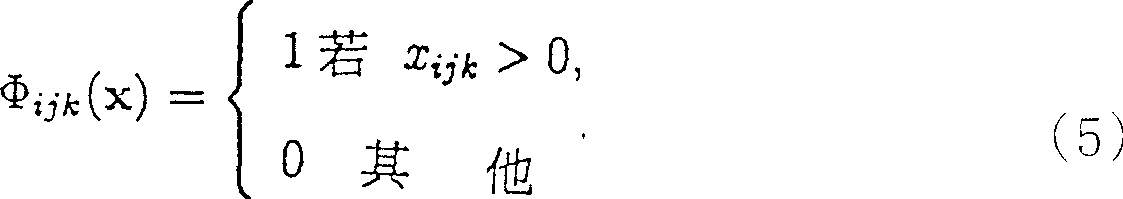
当把图象x转换为区带最大值图象时,根据数学式6,在i行j列象素的各区带值中,选择最大值。又,因前述区带最大值图象成为单区带图象,故在方便上,当作区带数1的前述图象来处理。因此,函数Bij1(x)的第3附加字为1。When the image x is converted into a zone maximum value image, according to
设图象x为二进制图象,当使图象x反转时,根据数学式7来进行计算。Assuming that the image x is a binary image, when inverting the image x, calculation is performed according to
Iijk(x)=1-Xijk (7)I ijk (x) = 1-X ijk (7)
图象X的位置p(i、j、k)的对数转换是根据数学式8来进行。式中,e是偏移(offset),是用来使自然对数函数的输出值达到有效范围,故一般e=1就可以。能由该对数化,将区带象素值彼此间的除算进行减算。又,设图象x为2n色调的数字图象111,若在存储器102上,具有查表(包含与区带数无关的2n个要素)的话,则不需每次计算自然对数函数,也不需具有标准的对数表。The logarithmic conversion of the position p(i, j, k) of the image X is performed according to
Lijk(x)=ln(xijk+e) (8)L ijk (x)=ln(x ijk +e) (8)
又,图象的位置p(i、j、k)的q附近位置的集合pijk(q)是用数学式9来表示。式中,q是4、8、24、48、80、120、(2r+1)2-1的连续数列,r是自然数。又,当超出图象大小的位置包含在集合pijk(q)的情形,只要没有特别指定,则能代用位置p(i、j、k)的。又,其他的情形,是依照指定,象素值相当于0,而且,代用图象所不含的虚构位置。借此能自动进行边缘处理。因此,集合Pijk(q)要素的数Nijk经常成为q。Also, the set pijk(q) of positions near q of the image position p(i, j, k) is represented by

因此,接下来,针对有关对应图象各区带象素值的最大8附近182的附近处理的函数及运算子,加以说明如下。Therefore, next, the functions and operators related to the neighborhood processing of the maximum 8
图象x的位置p(i、j、k)的平滑化是根据数学式10来进行。式中,int(v)是含有舍去实数v以下小数点。假如,图象x的区带象素值为整数值的话,则在组装硬件时,当Nijk=4时,对应xlmk的总和,将右移位指令变更为执行2次的电路,当Nijk=8时,对应xlmk的总和,将右移位指令变更为执行3次的电路,借此能省略执行除算的电路。The smoothing of the position p(i, j, k) of the image x is performed according to
虽是拉普拉斯算符(Laplacian)的计算,但如数学式11所示,这只是2阶差份运算子。8附近182是掌握噪声的微妙变化,零点及零交叉变多,正适合本发明。式中,因Nijk为4或8,故假如组装硬件时,当Nijk=4时,对应xijk,将左移位指令变更为执行2次的电路,当Nijk=8时,对应Xijk,将左移位指令变更为执行3次的电路,借此能省略执行乘算的电路。Although it is a Laplacian calculation, as shown in
根据由拉普拉斯算符所求出的值,来找出零点的方法而言,已知是找到从正变化到负的象素,但本发明,是根据数学式12,除了找到从负到正的零交叉象素外,经由从负到零或从零到正等零点,找到持续零的象素。在本发明,数学式12所找到的零点不是有边缘的场所,而是有噪声的场所,即,成为无边缘的场所。又,根据数学式12,实数值的二进制化也同时进行。According to the value obtained by the Laplacian operator, the method of finding the zero point is known to find pixels that change from positive to negative, but the present invention is based on
设图象x为任意的二进制图象,在图象x中,当弥补空孔的象素时,是根据数学式13来进行计算。式中,f是表示应弥补孔大小的参数,一般而言,f=1就可以。又,4附近的情形,因不能检知其性质上对角线,故较佳是尽量设定为8附近182。Let the image x be an arbitrary binary image. In the image x, when filling up empty pixels, the calculation is performed according to
设图象x为任意的二进制图象,在图象x中,当删除无孤立点的孤立孔时,是根据数学式14来进行计算。又,4附近的情形,因不能检知其性质上对角线,故较佳是尽量设定为8附近182。Let the image x be any binary image, in the image x, when deleting the isolated holes without isolated points, it is calculated according to
设图象x为任意的二进制图象,在图象x中,为了检知线宽为1的象素,使用4附近象素,根据数学式15来进行计算。Assuming that the image x is an arbitrary binary image, in order to detect a pixel with a line width of 1 in the image x, the calculation is performed according to
设2个图象x、y为任意的二进制图象,图象y是在图象x中,设为检知线宽为1的象素的图象,在图象x中,为了扩充线宽为1的象素线宽,使用4附近象素,根据数学式16来进行计算。Suppose two images x and y are arbitrary binary images, and image y is an image of a pixel whose detection line width is 1 in image x, in order to expand the line width The pixel line width of 1 is calculated according to
此处,若使用数学式15的线宽检知和数学式16的线宽扩充的话,则根据数学式17,能简单记述二进制图象的线宽互补。Here, if the detection of the line width of the
Cijk(x)=Kijk(x),J(x)) (17)C ijk (x) = K ijk (x), J(x)) (17)
其次,针对有关对应图象的各区带象素值的附近处理的函数及运算子,加以说明如下。Next, the functions and operators related to the neighborhood processing of pixel values corresponding to each region of the image are explained as follows.
当有2个图象x、y时,这些图象的最大值图象能根据数学式18来加以计算。When there are two images x, y, the maximum image of these images can be calculated according to
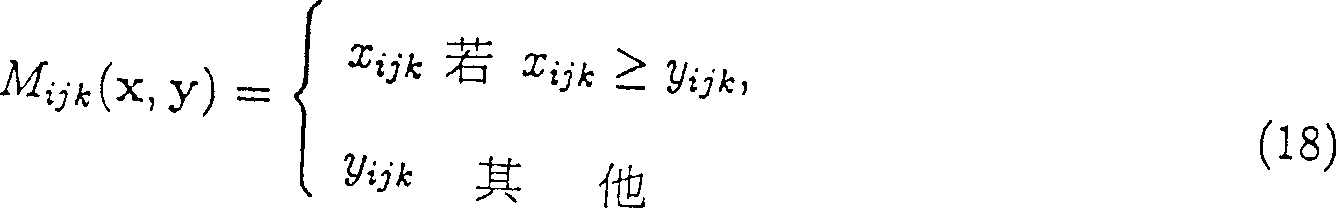
当有2个图象x、y时,这些图象的差份能根据数学式19来加以计算。When there are two images x, y, the difference between these images can be calculated according to
Dijk(x,y)=xijk-yijk (19)D ijk (x, y) = x ijk -y ijk (19)
式中,若使用数学式11的拉普拉斯算符和数学式19的差份的话,则能根据数学式20来简单记述图象组的鲜明化。In the formula, if the difference between the Laplace operator of the
Eijk(x)=Dijk(X,2 ijkX) (20)E ijk (x) = D ijk (X, 2 ijk X) (20)
当有2个图象x、y,图象y为单区带二进制图象时,根据数学式21,使用图象y的区带象素值,来取出图象x的各区带象素值。When there are two images x, y, and image y is a single-band binary image, according to
Oijk(x,y)=xijkyij1 (21)O ijk (x, y) = x ijk y ij1 (21)
当有2个图象x、y,图象x和y为二进制图象时,根据数学式22,能以图象x为基准,将图象y进行整形。When there are two images x, y, and the images x and y are binary images, according to Mathematical Formula 22, the image y can be reshaped based on the image x.

当有2个图象x、y,图象y为二进制图象时,根据数学式23,能在图象x的区带象素值附近,用图象y所指定的图象x的区带象素值平均值,将图象y所无指定的图象x的区带象素值加以内插。式中,int(v)是含有舍去实数v以下小数点的意。又,因图象y为二进制图象,分母为正数,故在存储器102中,存储从1到q的倒数,借此,能将整数的除算置换为实数的乘算。When there are two images x, y, and the image y is a binary image, according to the
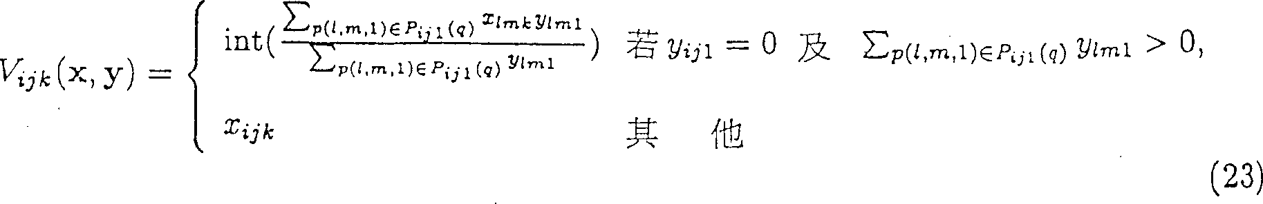
又,本发明,象素的位置及移动量等也由图象数据的处理,进行单纯处理。该处理称为位置的图象化。以下,针对有关位置图象化的一些函数及运算子加以说明。In addition, in the present invention, the position and movement amount of pixels are also simply processed by processing the image data. This process is called the visualization of the position. In the following, some functions and operators related to position imaging will be described.
首先,设位置p(l、m、o)的l、m、o各值为图象数据,设转换为区带象素值的运算子为#,被转换的区带象素值为#p(l、m、o)。其次,考虑区带象素值从位置p(i、j、k)移动到位置p(i+1、j+m、k+o)的情形。此时,区带象素值的移动量是用位置p(l、m、o)来表示者。即,移动量能视为来自某位置的向量。最后,把从区带象素值取出位置的运算子当做#-1。因此,#-1#p(l、m、o)=p(l、m、o)。First of all, assume that each value of l, m, and o in position p (l, m, o) is image data, set the operator converted into zone pixel value as #, and the converted zone pixel value is #p (l, m, o). Next, consider the case where the zone pixel value moves from position p(i,j,k) to position p(i+1,j+m,k+o). At this time, the movement amount of the zone pixel value is represented by the position p(l, m, o). That is, the movement amount can be regarded as a vector from a certain position. Finally, consider the operator that takes the position from the zone pixel value as #-1. Therefore, #-1#p(l, m, o)=p(l, m, o).
此处,根据数学式24,能用宽度方向和高度方向所显现的平面内,将移动量p(i、j、k)朝向180度相反方向。Here, according to
Υ(p(i,j,k))=p(-i,-j,k) (24)Υ(p(i,j,k))=p(-i,-j,k) (24)
当有图象x,图象x为单区带二进制图象时,朝图象x的位置p(i、j、k)的重心位置的移动量是根据数学式25来进行计算。又,本来,当计算重心时,虽需进行除算,但当计算往8附近182内的移动量时,因除算相抵消,故数学式25能省略除算。When there is an image x, and the image x is a single-zone binary image, the amount of movement toward the center of gravity of the position p (i, j, k) of the image x is calculated according to
从移动量p(i、j、k),根据数学式26、27及28,计算朝8附近182内的移动量,能加以图象化成移动量图象。又,数学式27及28是由图象的离散化,只使用在以数学式26对应不完的情形。From the amount of movement p(i, j, k), the amount of movement toward the vicinity of 8 182 is calculated according to the

因此,若使用数学式25、26、27及28的话,则根据数学式29、30及31,能简单记述朝单区带二进制图象x的重心方向移动量图象的区带象素值。又,移动量图象的区带数成为1。Therefore, if
Δij1(x)=θ(Gij1(x)) (29)Δ ij1 (x) = θ(G ij1 (x)) (29)
Δ’ij1(x)=θ’(Gij1(x)) (30)Δ' ij1 (x) = θ'(G ij1 (x)) (30)
Δ”ij1(x)=θ”(Gij1(x)) (31)Δ” ij1 (x) = θ” (G ij1 (x)) (31)
另一方面,若使用数学式24的话,因能求出重心位置的相反位置,故根据数学式32,能简单记述朝单区带二进制图象x的重心和相反方向的移动量图象的区带象素值。又,移动量图象的区带数成为1。On the other hand, if the
Rij1(x)=θ(Υ(Gij1(x))) (32)R ij1 (x)=θ(Υ(G ij1 (x))) (32)
当有2种图象x、y,图象y为移动量图象时,根据数学式33,将图象x的区带象素值移动到图象y所指示的移动位置后,能将移动到相同区带象素的区带象素值的总合设定为浓淡图象。When there are two kinds of images x, y, and image y is the moving amount image, according to mathematical formula 33, after the zone pixel value of image x is moved to the moving position indicated by image y, the moving The sum of zone pixel values to the same zone pixel is set as a shaded image.
Γijk(x,y)=∑xlmk在p(l,m,l)∈Pij1(q)及#-1ylm1=p(i-l,j-m,0)Γ ijk (x, y) = ∑ x lmk at p(l, m, l) ∈ P ij1 (q) and # -1 y lm1 = p(il, jm, 0)
(33)(33)
此处,由使用数学式5、29、30、31及33,根据数学式34、35及36,将单区带浓淡图象x移动到附近的重心方向后,能简单记述移动到相同区带象素的区带象素值的总合。Here, by using
Λij1(x)=Γij1(x,Δ(Ф(x))) (34)Λ ij1 (x) = Γ ij1 (x, Δ(Ф(x))) (34)
Λ’ij1(x)=Γij1(x,Δ’(Ф(x))) (35)Λ' ij1 (x) = Γ ij1 (x, Δ'(Ф(x))) (35)
Λ″ij1(x)=Γij1(x,Δ″(Ф(x))) (36)Λ″ ij1 (x) = Γ ij1 (x, Δ″(Ф(x))) (36)
又,在数学式33中,若附近数q被限定在8的话,则移动量图象y在各象素能从8附近182中,特别指定移动处。此处,图象x为冗余信息图象132,而且,如第12图所示,对应x的各象素的8附近182,以逆时针旋转,附加从l到8的号码时,从数学式37到数学式44的8个数学式,是分别在8个移动处,求出可能移动的图象x的区带象素值。Also, in Mathematical Expression 33, if the number of neighborhoods q is limited to 8, the movement amount image y can specify a movement location from 8


此处,使用数学式45、46及47,来取代数学式34、35及36,借此,从由8个移动处冗余信息183所构成的8区带浓淡图象x、及由冗余信息131所构成的单区带浓淡图象y,能产生8个各移动处的移动处冗余信息183。Here,
Λ* ijk(x,y)=Γijk(x,Δ(Ф(y)))+Γijk(Ф(y),Δ(Ф(y))) (45)Λ * ijk (x, y) = Γ ijk (x, Δ(Ф(y))) + Γ ijk (Ф(y), Δ(Ф(y))) (45)
Λ’* ijk(x,y)=Γijk(x,Δ’(Ф(y)))+Γijk(Ф(y),Δ’(Ф(y))) (46)Λ' * ijk (x, y) = Γ ijk (x, Δ'(Ф(y))) + Γ ijk (Ф(y), Δ'(Ф(y))) (46)
Λ”* ijk(x,y)=Γijk(x,Δ”(Ф(y)))+Γijk(Ф(y),Δ”(Ф(y))) (47)Λ” * ijk (x, y) = Γ ijk (x, Δ”(Ф(y)))+Γ ijk (Ф(y), Δ”(Ф(y))) (47)
又,根据条件,也能使用Γ* ijk(y,Δ(Ф(y)))来取代Γ* ijk(Ф(y),Δ(Ф(y)))。Also, depending on conditions, Γ * ijk (y, Δ(Ф(y))) can be used instead of Γ * ijk (Ф(y), Δ(Ф(y))).
当有2种图象x、y,图象x为二进制图象,图象y为移动量图象时,因能求出图象x的各区带象素值的移动处位置,故能找到移动处重复的区带象素值。此处,图象x的各区带象素值的移动处不是重复,而且表示移动的各区带象素值存在的可能移动图象的区带象素值是根据数学式48来产生。又,可能移动图象的区带数成为1。When there are two kinds of images x and y, image x is a binary image, and image y is a moving image, because the shift position of each zone pixel value of image x can be obtained, the moving position can be found. Repeated band pixel values at . Here, the moving positions of the pixel values of the regions of the image x are not repeated, and the pixel values of the regions of the possible moving image representing the existence of the pixel values of the moving regions are generated according to Mathematical Formula 48. Also, the number of zones in which a moving image can be moved is 1.
当有3种图象x、y、w,图象y为可能移动图象,图象w为移动量图象时,根据数学式49,能移动图象x的区带象素值。When there are three types of images x, y, and w, image y is a possible moving image, and image w is a moving amount image, according to Mathematical Formula 49, the region pixel value of image x can be moved.
此处,若使用数学式32、48及49的话,则根据数学式50,在与从二进制图象y计算所得的重心位置相反方向,能简单记述移动图象x的区带象素所得到图象的区带象素值。Here, if
Uijk(x,y)=Tijk(x,H(y,R(y)),R(y)U ijk (x, y) = T ijk (x, H(y, R(y)), R(y)
(50)(50)
此处,使用从数学式2到数学式50,借此,能记述组装第10图所示的图象存储机构12、颜色信息产生机构41、边缘信息产生机构14、边缘信息形成机构15、位置/大小检测机构17、位置/大小/倾斜检测机构44、区域正规化机构27、遮蔽机构40、及图象保持机构39的数据处理装置110的所有阵列运算单元100的算法。以下,使用数据处理装置110中的任意阵列运算单元100的算法,来说明图象存储机构12、颜色信息产生机构41、边缘信息产生机构14、边缘信息形成机构15、位置/大小检测机构17、位置/大小/倾斜检测机构44、区域正规化机构27、遮蔽机构40、及图象保持机构39。Here, by using
由数据处理装置110来实现的图象存储机构12,为了存储数字图象111,排列成格子状的阵列运算单元100是进行同步并列动作。设在格子上i行j列所配置的阵列运算单元100为AOUij,则AOUij的算法如第13图所示。In the
在步骤1201中,将AOUij配置在格子上的i行j列上。这是逻辑性也是物理性,是用来决定AOUij的附近所必要的。In step 1201, AOU ij is arranged on row i and column j on the grid. This is logical and physical, and it is necessary to determine the vicinity of AOU ij .
在步骤1202中,设定AOUij的附近和变数的初始值。In step 1202, the neighborhood of AOU ij and initial values of variables are set.
在步骤1203中,判断依序所输入的数字图象111是否变化。假如无数字图象111的话(步骤1203:是),则结束算法。假如有数字图象111话(步骤1203:否),则移行到步骤1204。但是,当只对应特别指定的图象大小,来组装阵列运算单元100时,即使设定为无限环路也可以。In step 1203, it is judged whether the sequentially input
在步骤1204中,数字图象111在准备前,等待输入。In step 1204, the
在步骤1205中,输入区带数份的数字图象111的i行j列的象素。因此,AOUij必须要有至少存储区带数份的图象数据的存储器102。In step 1205, the pixels of row i and column j of the
在步骤1206中,在输入等待期间,为了能输出,而存储数字图象111的i行j列的象素。In step 1206, during the waiting period for input, the pixels of row i and column j of
在步骤1207中,输出数字图象111的区带象素值。然后,返回步骤1203。In step 1207, the zone pixel values of the
借此,使用由阵列运算单元100所构成的数据处理装置110,图象存储机构12能存储数字图象111。Thereby, the
如第14图所示,由数据处理装置110所实现的颜色信息产生机构41,为了从数字图象111的各象素产生颜色信息171,排列成格子状的阵列运算单元100是进行同步并列动作。设在格子上i行j列所配置的阵列运算单元100为AOUij,则AOUij的算法如15图所示。As shown in FIG. 14, the color information generation mechanism 41 implemented by the
在步骤4101中,将AOUij配置在格子上的i行j列上。这是逻辑性也是物理性,是用来决定AOUij的附近所必要的。In step 4101, AOU ij is arranged on row i and column j on the grid. This is logical and physical, and it is necessary to determine the vicinity of AOU ij .
在步骤4102中,设定AOUij的附近和变数的初始值。In step 4102, the neighborhood of AOU ij and initial values of variables are set.
在步骤4103中,判断依序所输入的数字图象111是否变化。假如无数字图象111的话(步骤4103:是),则结束算法。假如有数字图象111的话(步骤4103:否),则移行到步骤4104。但是,当只对应特别指定的图象大小,来组装阵列运算单元100时,即使设定为无限环路也可以。In step 4103, it is judged whether the sequentially input
在步骤4104中,输入区带数份的数字图象111的i行j列的象素。因此,AOUij必须要有至少存储区带数份的图象数据的存储器102。In step 4104, the pixels of row i and column j of the
在步骤4105中,从数字图象111的i行j列的象素,抽出特别指定颜色,来产生颜色信息171。所产生的颜色信息171是当作颜色信息图象172的区带象素值来处理。In step 4105, a specified color is extracted from the pixels at row i and column j of the
在步骤4106中,输出颜色信息图象172的区带象素值。然后,返回步骤4103。In step 4106, the zone pixel values of the
借此,使用由阵列运算单元100所构成的数据处理装置110,颜色信息产生机构41能从数字图象111产生颜色信息图象172。Thereby, the color information generating means 41 can generate the
如第16图所示,由数据处理装置110所实现的边缘信息产生机构14,为了从数字图象111产生粗边缘信息图象113,排列成格子状的阵列运算单元100是进行同步并列动作。设在格子上i行j列所配置的阵列运算单元100为AOUij,则对应边缘信息产生机构14的AOUij的算法如17图所示。As shown in FIG. 16, the edge
在步骤1401中,将AOUij配置在格子上的i行j列上。这是逻辑性也是物理性,是用来决定AOUij的附近所必要的。In step 1401, AOU ij is arranged on row i and column j on the grid. This is logical and physical, and it is necessary to determine the vicinity of AOU ij .
在步骤1402中,设定AOUij的附近和变数的初始值。在附近的设定中,也可将前述各函数所使用的附近大/小q个别决定为4或8,也可将全部统一为4或8,本发明的边缘信息产生机构14为了提高所产生的粗边缘信息112的正确度,较佳是将附近大小q全部设定为8。但是,由用来产生粗边缘信息112的计算时间的限制、和数字图象111的区带数等,边缘信息产生机构14视需要,能由适当变化附近大小,来进行处置。In step 1402, the neighborhood of AOU ij and initial values of variables are set. In the setting of the vicinity, the nearby large/small q used by the above-mentioned functions can also be individually determined as 4 or 8, and can also be unified as 4 or 8. The edge
在步骤1403中,判断数字图象111是否结束。假如无数字图象111的话(步骤1403:是),则结束算法。假如有数字图象111的话(步骤1403:否),则移行到步骤1404。但是,当对应特别指定的区带数和图象大小,来组装阵列运算单元100时,即使设定为无限环路也可以。In step 1403, it is judged whether the
在步骤1404中,输入区带数份数字图象111的i行j列的象素。这是因为AOUij整批处理数字图象111的i行j列的象素的缘故。因此,AOUij至少必须要有存储区带数份的图象数据的存储器102。In step 1404, pixels in row i and column j of the
在步骤1405中,AOUij是与附近的阵列运算单元100进行通信,借此,对应所输入的数字图象111的各区带象素值,根据Sijk(x),进行平滑化。被平滑化的区带象素值是当作平滑化图象的区带象素值来处理。此处,函数Sijk(x)也可视需要,重复多次。一般的多区带图象的情形,该次数只要2次就可以。In step 1405, the AOU ij communicates with the adjacent
在步骤1406中,对应平滑化图象的各区带象素值,根据函数Lijk(x),进行对数转换。被对数转换的各区带象素值是当作对数转换图象的区带象素值来处理。In step 1406, the logarithmic transformation is performed according to the function L ijk (x) corresponding to the pixel values of each zone of the smoothed image. The logarithmically converted band pixel values are treated as band pixel values of the logarithmically transformed image.
在步骤1407中,AOUij是与附近的阵列运算单元100进行通信,借此,对应对数转换图象的各区带象素值,根据函数Eijk(x),进行鲜明化。被鲜明化的区带象素值是当作鲜明化图象的区带象素值来处理。又,当在数字图象111中,含有大量噪声时,能省略此步骤。In step 1407, the AOU ij communicates with the nearby
在步骤1408中,对应鲜明化图象的各区带象素值,根据函数Dijk(x,y),减去1输入前鲜明化图象的各区带象素值。计算差份的区带象素值是当作时间差份图象的区带象素值来处理。In step 1408, according to the function D ijk (x, y) corresponding to each area pixel value of the sharpened image, 1 is subtracted from each area pixel value of the sharpened image before input. The zone pixel values of the calculated difference are treated as the zone pixel values of the time difference image.
在步骤1409中,是用鲜明化图象所对应的各区带象素值,来置换1输入前鲜明化图象的各区带象素值。In step 1409, the corresponding region pixel values of the sharpened image are used to replace each region pixel value of the pre-input sharpened image.
在步骤1410中,AOUij是与附近的阵列运算单元100进行通信,借此,对应时间差份图象的各区带象素值,根据运算子2 ijk(x),进行拉普拉斯算符的计算。计算拉普拉斯算符的区带象素值是当作时间差份拉普拉斯算符图象的区带象素值来处理。In step 1410, the AOU ij communicates with the nearby
在步骤1411中,AOUij是与附近的阵列运算单元100进行通信,借此,对应时间差份拉普拉斯算符图象的各区带象素值,根据函数Zijk(x),抽出零点。抽出零点的区带象素值是当作时间差份零点图象的区带象素值来处理。In step 1411, the AOU ij communicates with the nearby
在步骤1412中,是对应时间差份拉普拉斯算符图象的各区带象素值,根据函数Bijk(x),检测出各区带象素值中的最大值。所检测出的最大值区带象素值是当作最大值时间差份零点图象的区带象素值来处理。又,为了方便起见,区带数为1。In step 1412, the maximum value of the pixel values in each zone is detected according to the function B ijk (x) corresponding to the pixel values in each zone of the Laplacian operator image of the time difference. The detected maximum zone pixel value is treated as the zone pixel value of the maximum time difference zero point image. Also, the number of zones is set to one for convenience.
在步骤1413中,AOUij是与附近的阵列运算单元100进行通信,借此,对应鲜明化图象的各区带象素值,根据运算子2 ijk(x),进行拉普拉斯算符的计算。计算拉普拉斯算符的区带象素值是当作拉普拉斯算符图象的区带象素值来处理。In step 1413, the AOU ij communicates with the nearby
在步骤1414中,AOUij是与附近的阵列运算单元100进行通信,借此,对应拉普拉斯算符图象的各区带象素值,根据函数Zijk(x),抽出零点。抽出零点的区带象素值是当作零点图象的区带象素值来处理。In step 1414, the AOU ij communicates with the nearby
在步骤1415中,是对应拉普拉斯算符图象的各区带象素值,根据函数Bij1(x),检测出各区带象素值中的最大值。所检测出的最大值区带象素值是当作最大值零点图象的区带象素值来处理。又,为了方便起见,区带数为1。In step 1415, corresponding to the pixel values of each zone of the Laplacian operator image, the maximum value among the pixel values of each zone is detected according to the function B ij1 (x). The detected maximum value zone pixel values are treated as zone pixel values of the maximum value zero point image. Also, the number of zones is set to one for convenience.
在步骤1416中,是对应拉普拉斯算符图象的各区带象素值和时间差份拉普拉斯算符图象的各区带象素值,根据函数Mijk(x,y),检测出位于各图象相同位置的区带象素值中的最大值。所检测出的最大值区带象素值是当作混合零点图象的区带象素值来处理。又,为了方便起见,区带数为1。In step 1416, corresponding to each zone pixel value of the Laplacian operator image and each zone pixel value of the time difference Laplacian operator image, according to the function M ijk (x, y), detect Find the maximum value of the zone pixel values located at the same position in each image. The detected maximum zone pixel value is treated as the zone pixel value of the mixed null image. Also, the number of zones is set to one for convenience.
在步骤1417中,AOUij是与附近的阵列运算单元100进行通信,借此,对应混成零点图象的区带象素值,根据函数Fijk(x),将孔加以除去。被除去孔的区带象素值是当作孔除去混成零点图象的区带象素值来处理。又,为了方便起见,区带数为1。此处,函数Fijk(x),也可视需要重多个次。一般的多区带图象的情形,此次数1次就可以。In step 1417, the AOU ij communicates with the nearby
在步骤1418中,AOUij是与附近的阵列运算单元100进行通信,借此,对应孔除去混成零点图象的区带象素值,根据函数Aijk(x),将孤立点及孤立孔加以除去。被除去孤立点及孤立孔的区带象素值当作噪声除去混成零点图象的区带象素值来处理。又,为了方便起见,区带数为1。In step 1418, the AOU ij communicates with the nearby
在步骤1419中,对应噪声除去混成零点图象的区带象素值,根据函数Iijk(x),使0和1反转。被反转的区带象素值当作粗边缘信息图象113的区带象素值来处理。In
在步骤1420中,输出粗边缘信息图象113的区带象素值。然后,返回步骤1403。In step 1420, the region pixel values of the rough
借此,使用由阵列运算单元100构成的数据处理装置110,边缘信息产生机构14能从数字图象111产生粗边缘信息图象113。Thereby, using the
如第18图所示,由数据处理装置110所实现的边缘信息形成机构15,为了产生由粗边缘信息112所构成的粗边缘信息图象113、和数字图象111、和由形成边缘信息114所构成的形成边缘信息图象115,排列成格子状的阵列运算单元100是进同步并列动作。设在格子上i行j列所配置的阵列运算单元100为AOUij,则AOUij的算法如19图所示。As shown in Figure 18, the edge
步骤1501中,将AOUij配置在格子上的i行j列上。这是逻辑性也是物理性,是用来决定AOUij的附近所必要的。In step 1501, AOU ij is arranged on row i and column j on the grid. This is logical and physical, and it is necessary to determine the vicinity of AOU ij .
在步骤1502中,设定AOUij的附近和变数的初始值。在附近的设定中,也可将前述各函数所使用的附近大小q个别决定为4或8,也可将全部统一为4或8,本发明的边缘信息形成机构15为了提高所形成的形成边缘信息114的正确度,较佳是将附近大小q全部设定为8。但是,由用来形成粗边缘信息112的计算时间的限制、和所输入的数字图象111的区带数等,借此边缘信息形成机构15视需要,能适当变化附近大小,来进行处置。In step 1502, the neighborhood of AOU ij and initial values of variables are set. In the setting of the neighborhood, the neighborhood size q used by each of the aforementioned functions can also be individually determined as 4 or 8, or all of them can be unified as 4 or 8. The edge
在步骤1503中,判断依序所输入的数字图象111或粗边缘信息图象113是否变化。假如无数字图象111或粗边缘信息图象113的话(步骤1503:是),则结束算法。假如有数字图象111或粗边缘信息图象113的话(步骤1503:否),则移行到步骤1504。但是,当对应特别指定的区带数和图象大小,来组装阵列运算单元100时,即使设定为无限环路也可以。In step 1503, it is judged whether the sequentially input
在步骤1504中,输入区带数份数字图象111及粗边缘信息图象113的i行j列的象素。这是因为AOUij整批处理数字图象111及粗边缘信息图象113的i行j列的象素的故。因此,AOUij至少必须要有存储区带数份的图象数据的存储器102。In step 1504, pixels in row i and column j of the
在步骤1505中,将数字图象111的i行j列的象素与粗边缘信息图象113的i行j列的象素加以分离。这是因为AOUij将数字图象111的i行j列的象素与粗边缘信息图象113的i行j列的象素当作各自独立的图象象素来处理的故。假如,数字图象111的i行j列的象素与粗边缘信息图象113的i行j列的象素从开始便被分离输入的话,则无特别进行。In step 1505, the pixels of row i and column j of the
在步骤1506中,AOUij是与附近的阵列运算单元100进行通信,借此,对应所输入的数字图象111的各区带象素值,根据Sijk(x),进行平滑化。被平滑化的各区带象素值是作为平滑化图象的区带象素值处理。此处,函数Sijk(x)也可视需要,重复多次。一般的多区带图象的情形,该次数只要2次就可以。In step 1506, the AOU ij communicates with the nearby
在步骤1507中,对应平滑化图象的各区带象素值,根据函数Lijk(x),进行对数转换。被对数转换的各区带象素值是当作对数转换图象的区带象素值来处理。In step 1507, the logarithmic conversion is performed according to the function L ijk (x) corresponding to the pixel values of each zone of the smoothed image. The logarithmically converted band pixel values are treated as band pixel values of the logarithmically transformed image.
在步骤1508中,AOUij是与附近的阵列运算单元100进行通信,借此,对应对数转换图象的各区带象素值,根据函数Eijk(x),进行鲜明化。被鲜明化的区带象素值是当作鲜明化图象的区带象素值来处理。又,当在数字图象111中,含有大量噪声时,能省略此步骤。In step 1508, the AOU ij communicates with the nearby
在步骤1509中,AOUij是与附近的阵列运算单元100进行通信,对应鲜明化图象的各区带象素值,根据运算子2 ijk(x),进行拉普拉斯算符的计算。计算拉普拉斯算符的区带象素值是当作拉普拉斯算符图象的区带象素值来处理。In step 1509, the AOU ij communicates with the nearby
在步骤1510中,AOUij是与附近的阵列运算单元100进行通信,借此,对应拉普拉斯算符图象的各区带象素值,根据函Zijk(x),抽出零点。抽出零点的区带象素值是当作零点图象的区带象素值来处理。In step 1510, the AOU ij communicates with the nearby
在步骤1511中,对应零点图象的各区带象素值,根据函数Bijk(x),在各区带象素值中,检测出最大值。所检测出的最大区带象素值是当作最大值零点图象的区带象素值来处理。又,为了方便起见,区带数为1。In step 1511, corresponding to the pixel values of each zone of the zero-point image, according to the function B ijk (x), the maximum value is detected among the pixel values of each zone. The detected maximum zone pixel value is treated as the zone pixel value of the maximum value null image. Also, the number of zones is set to one for convenience.
在步骤1512中,对应最大值零点图象的区带象素值,根据函数Iijk(x),反转0和1。被反转的区带象素值是当作基础边缘信息图象的区带象素值来处理。In
在步骤1513中,所输入的粗边缘信息图象113的区带象素值是当作第1次整形粗边缘信息图象的区带象素值来处理,AOUij是与附近的阵列运算单元100进行通信,借此,使用基础边缘信息图象的区带象素值,对应整形粗边缘信息图象的各区带象素值,根据函数Qijk(x,y),进行整形。被整形的区带象素值是再当作整形粗边缘信息图象的区带象素值来处理,此处,函数Qijk(x,y)本来是重复到整形粗边缘信息图象的区带象素值不变化。但是,由于计算时间的限制、所输入的粗边缘信息图象113的品质、所形成的形成边缘信息图象115所求出的品质等,故较佳是整形处理以适当的重复次数来结束计算。In step 1513, the zone pixel value of the input rough
在步骤1514中,AOUij是与附近的阵列运算单元100进行通信,借此,对应整形粗边缘信息图象的区带象素值,根据函数Cijk(x),进行线宽互补。被互补后的区带象素值是当作形成边缘信息图象115的区带象素值来处理。In step 1514, the AOU ij communicates with the nearby
在步骤1515中,输出形成边缘信息图象115的区带象素值。然后,返回步骤1503。In step 1515, the region pixel values forming the
借此,使用由阵列运算单元100所构成的数据处理装置110,边缘信息形成机构15能将粗边缘信息图象113形成为形成边缘信息图象115。Thereby, the edge
此处,所谓从粗边缘信息图象113到形成边缘信息图象115的形成,是从摄象某场面的低解析度的数字图象111所产生的边缘信息,能视为推定从摄象相同场面的高解析度的数字图象111所应产生的边缘信息。此处,对应自然数n,如第20图所示,当从把数字图象111降低到1/n的低解析度数字图象116,使用边缘信息产生机构14,产生低解析度粗边缘信息图象117时,将低解析度粗边缘信息图象117放大n倍,借此,能产生粗边缘信息图象113。但是,为了将数字图象111的解析度设定为1/n,也可对应水平及垂直方向,单纯在数字图象111的连续n个中,抽出1个。又,为了将低解析度粗边缘信息图象117放大n倍,较佳是对应水平及垂直方向,单纯在低解析度粗边缘信息图象117的连续象素间,弥补n-1个区带象素值为0的象素。此时,若n不太大的话,则实现边缘信息形成机构15的数据处理装置110,其形成粗边缘信息图象113(将低解析度粗边缘信息图象117放大)形成边缘信息图象115、和实现边缘信息形成机构15的数据处理装置110,由数字图象111所产生的粗边缘信息图象113的形成边缘信息图象115是几乎相同的。其理由是边缘信息形成机构15使用数字图象111,在内部所产生的边缘信息中,为了使用哪种边缘信息来作为参考,边缘信息形成机构15只使用粗边缘信息图象113的故。因此,当把低解析度粗边缘信息图象117放大的粗边缘信息图象113输入到边缘信息形成机构15时,实现边缘信息产生机构14(从低解析度数字图象116产生低解析度粗边缘信息图象117)的数据处理装置110,能减低计算量或硬件量。Here, the so-called formation from the rough
又,若使该方法发展的话,则如第21图所示,在从低解析度数字图象116(降低数字图象111的解析度)所产生的低解析度粗边缘信息图象117之中,能产生切出粗边缘信息112周边的低解析度切出粗边缘信息图象118。若将该低解析度切出粗边缘信息图象118加以放大的切出粗边缘信息图象119、和数字图象111中切出相同区域的切出数字图象120,输入到实现边缘信息形成机构15的数据处理装置110的话,则能产生切出形成边缘信息图象121。该情形,实现边缘信息形成机构15的数据处理装置110能减低硬件量。视觉装置2,切出数字图象120也能视为以经常在数字图象111之中央变化的方式来使移动摄象机10的方向及倍率变化。Also, if this method is developed, as shown in FIG. 21, in the low-resolution rough
如第22图所示,由数据处理装置110所实现的位置/大小检测机构17,为了从粗边缘信息图象113(把粗边缘信息112当作象素),产生冗余信息图象132(把冗余信息131当作象素),排列成格子状的阵列运算单元100是进行同步并列动作。设在格子上i行j列所配置的阵列运算单元100为AOUij,则AOUij的算法如第23图所示。As shown in Fig. 22, the position/
在步骤1701中,将AOUij配置在格子上的i行j列上。这是逻辑性也是物理性,是用来决定AOUij的附近所必要的。In step 1701, AOU ij is arranged on row i and column j on the grid. This is logical and physical, and it is necessary to determine the vicinity of AOU ij .
在步骤1702中,设定AOUij的附近和变数的初始值。在附近的设定中,可以个别决定前述各函数所使用的附近大小q,也可统一全部。本发明的数据处理装置110为了提高所产生的冗余信息图象132的正确度,较佳是将附近大小q所有设定为大的值。但是,因用来计算物体的粗边缘信息112的重心的计算时间的限制、和所输入的粗边缘信息图象113的大小等,位置/大小检测机构17是视需要,能适当改变附近大小,来加以对应。In step 1702, the neighborhood of AOU ij and initial values of variables are set. In the setting of the neighborhood, the size q of the neighborhood used by each of the above-mentioned functions may be individually determined, or all of them may be unified. In order to improve the accuracy of the generated
在步骤1703中,判断依序所输入的粗边缘信息图象113是否变化。假如无粗边缘信息图象113的话(步骤1703:是),则结束算法。假如有粗边缘信息图象113的话(步骤1703:否),则移行到步骤1704。但是,当只对应特别指定的图象大小,来组装阵列运算单元100时,即使设定为无限环路也可以。In step 1703, it is judged whether the sequentially input rough
在步骤1704中,输入1区带份的粗边缘信息图象113的i行j列的象素。因此,AOUij必须要有至少存储1区带份的图象数据的存储器102。In step 1704, the pixels at row i and column j of the rough
在步骤1705中,将粗边缘信息图象113的粗边缘信息112转换为冗余信息图象132的冗余信息131。冗余信息131成为相当于1或0的区带象素值。In step 1705, the
在步骤1706中,AOUij是与附近的阵列运算单元100进行通信,借此,对应冗余信息图象132的各区带象素值,根据函数Δij1(x),计算移动量。将移动量进行图象化的区带象素值当作移动量图象的区带象素值来处理。In step 1706, the AOU ij communicates with the nearby
在步骤1707中,AOUij是与附近的阵列运算单元100进行通信,借此,对应冗余信息图象132的各区带象素值,根据函数Λij1(x),使移动量移动到指示处。将所移动的区带象素值当作新的冗余信息图象132的区带象素值来处理。In step 1707, the AOU ij communicates with the nearby
在步骤1708中,判断表示从步骤1706到步骤1707的重复次数的移动次数是否达到指定次数。假如,移动次数不能达到指定次数的话(步骤1708:否),则返回步骤1706。假如,移动次数能达到指定次数的话(步骤1708:是),则移行到步骤1709。又,该指定次数是由形成边缘信息图象115的大小和形成边缘信息114所显现的物体的大小,及附近大小q来决定。若视使用目的,设定适当的参数的话,则即使多些决定指定次数,也无问题,若指定次数太多的话,则检测出位置及大小所需要的时间就会变长。In step 1708, it is judged whether or not the number of shifts representing the number of repetitions from step 1706 to step 1707 has reached a specified number of times. If the number of times of movement cannot reach the specified number of times (step 1708: No), then return to step 1706. If the number of times of movement can reach the specified number of times (step 1708: Yes), then move to step 1709. In addition, the specified number of times is determined by the size of the image forming the
在步骤1709中,AOUij是与附近的阵列运算单元100进行通信,借此,对应冗余信息图象132的各区带象素值,根据函数Δ’ij1(x),计算移动量。将移动量进行图象化的区带象素值是当作移动量图象的区带象素值来处理。In step 1709, the AOU ij communicates with the adjacent
在步骤1710中,AOUij是与附近的阵列运算单元100进行通信,借此,对应冗余信息图象132的各区带象素值,根据函数Λ’ij1(x),使移动量移动到指示处。所移动的区带象素值是当作新的冗余信息图象132的区带象素值来处理。In step 1710, the AOU ij communicates with the nearby
在步骤1711中,输出冗余信息图象132的区带象素值。然后,返回步骤1703。In step 1711, the region pixel values of the
又,因冗余信息图象132的各冗余信息131是表示位于以其位置为中心的周边的粗边缘信息112的总数,故其结果,意味着以其位置为中心的物体的大小。Also, since each
借此,使用由阵列运算单元100所构成的数据处理装置110,位置/大小检测机构17能从粗边缘信息图象113产生冗余信息图象132。Thereby, using the
此处,在第23图的算法中,若使用表示物体区域141的物体区域图象142,来取代由粗边缘信息112所构成的粗边缘信息图象113的话,则如第24图所示,由数据处理装置110所实现的位置/大小检测机构17也能从表示物体区域141的物体区域图象142来产生表示冗余信息131的冗余信息图象132。但是,当使用物体区域图象142时,因冗余信息图象132的各冗余信息131是表示把其位置当作中心的物体区域141的象素的总数,故其结果,意味着以其位置为中心的物体的面积。因此,当从冗余信息图象132求出物体大小时,要注意取冗余信息131的平方根等。又,当使用形成边缘信息图象115及颜色信息图象172时也是同样。Here, in the algorithm in FIG. 23, if the
又,如第25图所示,由数据处理装置110所实现的位置/大小/倾斜检测机构44,为了从粗边缘信息图象113(把粗边缘信息112当作象素),产生冗余信息图象132(把冗余信息131当作象素),排列成格子状的阵列运算单元100是进行同步并列动作。设在格子上i行j列所配置的阵列运算单元100为AOUij,则AOUij的算法如第26图所示。Also, as shown in FIG. 25, the position/size/
在步骤4401中,将AOUij配置在格子上的i行j列上。这是逻辑性也是物理性,是用来决定AOUij的附近所必要的。In step 4401, AOU ij is arranged on row i and column j on the grid. This is logical and physical, and it is necessary to determine the vicinity of AOU ij .
在4402中,设定AOUij的附近和变数的初始值。在附近的设定中,可以个别决定前述各函数所使用的附近大小q,也可统一全部。本发明的数据处理装置110为了提高所产生的冗余信息图象132的正确度,较佳是将附近大小q所有设定为大的值。但是,因用来计算物体的粗边缘信息112的重心等的计算时间的限制、和所输入的粗边缘信息图象113的大小等,位置/大小/倾斜检测机构44是视需要,能适当改变附近大小,来加以对应。In 4402, the neighborhood of AOU ij and initial values of variables are set. In the setting of the neighborhood, the size q of the neighborhood used by each of the above-mentioned functions may be individually determined, or all of them may be unified. In order to improve the accuracy of the generated
在步骤4403中,判断依序所输入的粗边缘信息图象113是否变化。假如无粗边缘信息图象113的话(步骤4403:是),则结束算法。假如有粗边缘信息图象113的话(步骤4403:否),则移行到步骤4404。但是,当只对应特别指定的图象大小来组装阵列运算单元100时,即使设定为无限环路也可以。In step 4403, it is judged whether the sequentially input rough
在步骤4404中,输入1区带份的粗边缘信息图象113的i行j列的象素。因此,AOUij必须要有至少存储1区带份的图象数据的存储器102。In step 4404, the pixels of row i and column j of the rough
在步骤4405中,将粗边缘信息图象113的粗边缘信息112转换为冗余信息图象132的冗余信息131。冗余信息131成为相当于1或0的区带象素值。又,8个移动处冗余信息183是用相当于0的区带象素值来进行清除。In step 4405, the
在步骤4406中,AOUij是与附近的阵列运算单元100进行通信,借此,对应冗余信息图象132的各区带象素值,根据函数Δij1(x),计算移动量。将移动量进行图象化的区带象素值是当作移动量图象的区带象素值来处理。In step 4406, the AOU ij communicates with the adjacent
在步骤4407中,AOUij是与附近的阵列运算单元100进行通信,借此,对应移动处冗余信息图象184的各区带象素值,根据函数Λ*ij1(x,y),使移动量移动到指示处。所移动的区带象素值是当作新的移动处冗余信息图象184的区带象素值来处理。In step 4407, the AOU ij communicates with the nearby
在步骤4408中,AOUij是与附近的阵列运算单元100进行通信,借此,对应冗余信息图象132的各区带象素值,根据函数Λij1(x),使移动量移动到指示处。所移动的区带象素值是当作新的冗余信息图象132的区带象素值来处理。In step 4408, the AOU ij communicates with the nearby
在步骤4409中,判断表示从步骤4406到步骤4408的重复次数的移动次数是否达到指定次数。假如,移动次数不能达到指定次数的话(步骤4409:否),则返回步骤4406。假如,移动次数能达到指定次数的话(步骤4409:是),则移行到步骤4410。该指定次数是由粗边缘信息图象113的大小和粗边缘信息112所显现的物体大小,及附近大小q来决定。若视使用目的,设定适当的参数的话,则即使多些决定指定次数,也没问题,若指定次数太多的话,则检测出位置、大小及倾斜所需要的时间就会变长。In step 4409, it is judged whether the number of moves representing the number of repetitions from step 4406 to step 4408 has reached a specified number of times. If the number of times of movement cannot reach the specified number of times (step 4409: No), then return to step 4406. If the number of times of movement can reach the specified number of times (step 4409: Yes), then move to step 4410. The specified number of times is determined by the size of the rough
在步骤4410中,AOUij是与附近的阵列运算单元100进行通信,借此,对应冗余信息图象132的各区带象素值,根据函数Δ’ij1(x),计算移动量。将移动量进行图象化的区带象素值是当作移动量图象的区带象素值来处理。In step 4410, the AOU ij communicates with the adjacent
在步骤4411中,AOUij是与附近的阵列运算单元100进行通信,借此,对应移动处冗余信息图象184的各区带象素值,根据函数Λ’* ijk(x,y),使移动量移动到指示处。所移动的区带象素值是当作新的移动处冗余信息图象184的区带象素值来处理。In step 4411, the AOU ij communicates with the nearby
在步骤4412中,AOUij是与附近的阵列运算单元100进行通信,借此,对应冗余信息图象132的各区带象素值,根据函数Λ’ij1(x),使移动量移动到指示处。所移动的区带象素值是当作新的冗余信息图象132的区带象素值来处理。In step 4412, the AOU ij communicates with the nearby
在步骤4413中,判断表示从步骤4406到步骤4412的重复次数的缩退次数是否达到指定次数。假如,缩退次数不能达到指定次数的话(步骤4413:否),则返回步骤4406。假如,缩退次数能达到指定次数的话(步骤4413:是),则移行到步骤4414。又,该指定次数是由粗边缘信息图象113的大小和粗边缘信息112所显现的物体大小,及附近大小q来决定。若视使用目的,设定适当的参数的话,则即使多些决定指定次数,也没问题,若指定次数太多的话,则检测出位置、大小及倾斜所需要的时间就会变长。In step 4413, it is judged whether or not the number of retractions representing the number of repetitions from step 4406 to step 4412 has reached a specified number of times. If the number of withdrawals cannot reach the specified number of times (step 4413: No), then return to step 4406. If the number of retreats can reach the specified number of times (step 4413: Yes), then move to step 4414. In addition, the specified number of times is determined by the size of the rough
在步骤4414中,输出冗余信息图象132的区带象素值及移动处冗余信息图象184的各区带象素值。然后,返回步骤4403。In step 4414, the region pixel values of the
又,因冗余信息图象132的各冗余信息131是表示位于以该位置为中心的周边的粗边缘信息112的总数,故其结果,意味着以该位置为中心的物体的大小。又,因只在有冗余信息131的象素,有移动处冗余信息183,故其结果,意味着以该位置为中心的物体的倾斜。Also, since each
借此,使用由阵列运算单元100所构成的数据处理装置110,位置/大小/倾斜检测机构44能从粗边缘信息图象113,产生冗余信息图象132及移动处冗余信息图象184。但是,假如,该冗余信息图象132所显现的物体的大致重心位置,若偏移实际重心位置太大的话,则较佳是在步骤4410中,交互使用函数Δ’ij1(x)及函数Δ”ij1(x)。同样地,在步骤4411中,交互使用函数Λ’* ijk(x,y)及Λ’* ijk(x,y),在步骤4412中,较佳是交互使用函数Λ’ij1(x)及Λ”ij1(x,y)。Thereby, using the
此处,在第26图的算法中,也能使用由形成边缘信息114所构成的形成边缘信息图象115,来取代由粗边缘信息112所构成的粗边缘信息图象113。又,若使用表示物体区域141的物体区域图象142,来取代由粗边缘信息112所构成的粗边缘信息图象113的话,则如第27图所示,位置/大小/倾斜检测机构44,也能从表示物体区域141的物体区域图象142,产生冗余信息图象132及移动处冗余信息图象184。但是,当使用物体区域图象142时,因冗余信息图象132的各冗余信息131是表示以该位置为中心的物体区域141的象素的总数,故其结果,意味着以该位置为中心的物体的面积。因此,当从冗余信息图象132来求出物体的大小时,要注意取冗余信息131的平方根。使用由颜色信息(表示物体的特别指定颜色的有无)所构成的颜色信息图象172来取代物体区域图象142的情形也是同样。Here, in the algorithm shown in FIG. 26, the formed
以上,是针对从粗边缘信息图象113、形成边缘信息图象115、物体区域图象142及颜色信息图象172,产生移动处冗余信息图象184的方法,加以说明。至于以下,针对从移动处冗余信息183求出物体倾斜角度的方法加以说明。Above, the method for generating the
首先,设从第12图及第28图所示的附近1到附近8的移动处冗余信息183分别为N1~N8,则以逆时针旋转所显现的倾斜角度θ,例如,根据数学式51来求出。又,倾斜角度θ是用弧度来表示者,当物体是水平及垂直时,倾斜角度θ为0弧度。First, assuming that the

例如,当从N1到N8的移动处冗余信息183如第28图所示时,倾斜角度θ约成为-0.4弧度。数学式51是用来求出倾斜角度θ的简单数学式,当然,进行比数学式51更细的条件,借此,本发明的使用者能更正确求出倾斜角度θ。其他,为了求出对应水平的倾斜角度θ,使用数学式52。For example, when the
又,若该倾斜角度θ概略就可以的话,则函数arctan(y/x)不必使用对数表。例如,若该倾斜角度θ只要取0弧度、π/4弧度、π/2弧度及3π/4弧度中的任一弧度就可以的话,则函数arctan(y/x)也可使用数学式般近似值。Also, if the inclination angle θ is approximately sufficient, the function arctan(y/x) does not need to use a logarithmic table. For example, if the inclination angle θ can be any one of 0 radians, π/4 radians, π/2 radians and 3π/4 radians, then the function arctan(y/x) can also use a mathematical approximation .
此处,阵列运算单元100是计算数学式51及数学式52,若产生冗余信息131及由倾斜角度θ所构成的倾斜大小信息185的话,则阵列运算单元100与输出8个移动处冗余信息183的情形相较,能输出更少的数据量。例如,当倾斜角度θ被限定在4种时,若对应各自倾斜角度的冗余信息131被分配为个别的区带象素值的话,则倾斜大小信息图象186成为4区带图象。又,若4种的倾斜角度θ用1种的区带象素值来表示的话,则倾斜大小信息图象186成为2区带图象。其他,若倾斜角度θ也可用一定的刻度范围来表示的话,则存储器102也可只存储备有必要数倾斜角度的查表,来取代对数表。当然,阵列运算单元100也可使用数学式53般的近似函数。Here, the
然而,在第25图及第27图,是粗边缘信息图象113(含有分别对应1个物体所产生的粗边缘信息112)及物体区域图象142(含有物体区域141),是被输入到位置/大小/倾斜检测机构44,但当然,当在粗边缘信息图象113及物体区域图象142中,有多个物体的情形,位置/大小/倾斜检测机构44也能检测出各个物体的位置、大小及倾斜。而且,如第29图所示,颜色信息图象172成为结构时,位置/大小/倾斜检测机构44能从各个颜色信息171的块,检测出位置、大小及倾斜。因此,位置/大小/倾斜检测机构44也能利用在结构解析。However, in Fig. 25 and Fig. 27, the rough edge information image 113 (containing the
又,以上,是针对位置/大小/倾斜检测机构44加以说明。由前述的说明可知,若粗边缘信息图象113中的1个物体的轮廓能用多个等间隔的线段来表示的话,则位置/大小/倾斜检测机构44能从该粗边缘信息信息图象113,求出这些线段的长度及倾斜。但是,为了对应位于任意位置的任意物体,产生该粗边缘信息图象113,因另外必须要有使用多个大遮罩的特别图象处理装置,故实际上,位置/大小/及倾斜检测机构44是对应1个物体,否则,只能输入含少数线段的粗边缘信息图象113或形成源信息图象115。因此,位置/大小/倾斜检测机构44是限定使用前述的方法,从这些粗边缘信息图象113,不能求出表示1个物体轮廓的多个线段的长度及倾斜。In addition, the above description is for the position/size/
但是,当位置/大小/倾斜检测机构44只执行对应8附近182的局部处理时,即,在第26图的步骤4406及步骤4410中,当附近大小q为8时,位置/大小/倾斜检测机构44是根据条件,有时能求出粗边缘信息图象113中的粗边缘信息112所构成的多个线段及曲线的法线方向。特别是粗边缘信息图象113中的多个线段及曲线的线宽概略为2或3象素时,即,对应形成边缘信息114,位置/大小/倾斜检测机构44是确实将这些线段及曲线分割成一定量以下的形成边缘信息114,能进一步求出这些线段及曲线的法线方向角度。例如,第31图的情形,位置/大小/倾斜检测机构44是相对于水平,相对于135度倾斜的形成边缘信息图象115中的线段,相对于水平,输出45度的角度。当然,位置/大小/倾斜检测机构44所输出的物体的大小是相对于水平,成为倾斜135度线段的长度。又,第32图的情形,位置/大小/倾斜检测机构44将形成边缘信息图象115中的十字形分割成5种线段后,相对于形成边缘信息图象115中的水平线段,相对于水平输出90度的角度,相对于形成边缘信息图象115中的垂直线段,相对于水平输出0度的角度。其次,第33图的情形,位置/大小/倾斜检测机构44是将形成边缘信息图象115中的三角形分割成6个线段,分别输出法线方向的角度。其次,第34图的情形,位置/大小/倾斜检测机构44是将形成边缘信息图象115中的四角形分割成8个线段,分别输出法线方向的角度。又,由第34图可知,四角形的4个角,分别转换为倾斜该四角形重心方向的短的线段。其次,第35图的情形,位置/大小/倾斜检测机构44是将形成边缘信息图象115中的90度倾斜的四角形(此处,叫作棱形)分割成6个线段,分别输出法线方向的角度。最后,第36图的情形,位置/大小/倾斜检测机构44是将形成边缘信息图象115中的圆形分割成8个线段,分别输出法线方向的角度。此处,若位置/大小/倾斜检测机构44使用数学式54,在这些法线方向的角度,加90度的话,则位置/大小/倾斜检测机构44能求出表示形成边缘信息图象115中的物体轮廓的多个线段及曲线的切线方向的角度。However, when the position/size/
又,若位置/大小/倾斜检测机构44是视为输出多个线段及曲线(表示形成边缘信息图象115中的物体轮廓)的法线方同的角度者和几何解析机构37的话,则位置/大小/倾斜检测机构44也可使用数学式52。Also, if the position/size/
此处,对应形成边缘信息图象115中的所有各种物体,若能将位置/大小/倾斜检测机构44所输出的倾斜大小信息图象186的倾斜大小信息185集中在几何解析机构37的1处的话,则几何解析机构37就能识别该物体的形状。因此,将多个信息集中在一处的方法业已由位置/大小/倾斜检测机构44来加以实现。但是,与1个物体有关联的倾斜大小信息185,因分散在倾斜大小信息图象186中,故如第29图所示,几何解析机构37要用与位置/大小/倾斜检测机构44同样的方法,不易将倾斜大小信息185集中在一处。因此,以下,针对利用形成边缘信息图象115,将倾斜大小信息185集中在1处的位置/大小/形状检测机构45加以说明。Here, corresponding to all various objects forming in the
首先,将数学式37~44分别扩充到数学式55~62。式中,k是取得倾斜大小信息185所显现的线段的倾斜角度θ的0度以上180度以下的范围被区分为多个区域的情形,表示各自区域所分配的号码。例如,当倾斜角度θ被区分为0度、45度、90度及135度4种的区域情形,k=0时,k是表示0度的区域,k=1时,k是表示45度的区域,k=2时,k是表示90度的区域,k=3时,k是表示135度的区域。First, extend the


当然,也能将倾斜角度θ区分为任意数的区域,以下,为了简单说明,设使用该条件。在数学式56~62中,若k为0的话,则数学式56~62分别成为数学式37~44。因此,在位置/大小/倾斜检测机构44中,的个阵列运算单元100能分别使用数学式55~62来取代数学式37~44。Of course, the inclination angle θ can also be divided into an arbitrary number of regions, and in the following, for the sake of simplicity of description, this condition is assumed to be used. In
其次,数学式63是被追加于数学式55~62。该数学式63是在倾斜大小信息图象186中,被用来计算倾斜角度θ的各区域所含的倾斜大小信息185所显现的线段的长度的总合。Next,
Γ** i,j,9k+9(x,y)=0 (63)Γ ** i, j, 9k+9 (x, y) = 0 (63)
此处,使用数学式64、65及66来取代数学式45、46及47,借此,从由36个移动处倾斜冗余信息187所构成的36区带浓淡图象x和由冗余信息131所构成的单区带浓淡图象y,在各倾斜角度θ的各区域,产生每8个移动处的移动处倾斜冗余信息187、和表示倾斜大小信息185所显现的线段长度总合的移动处倾向冗余信息187。Here,
Λ** ijk(x,y)=Γijk(x,Δ(Ф(y)))+Γ** ijk(Ф(y),Δ(Ф(y))) (64)Λ ** ijk (x, y) = Γ ijk (x, Δ(Ф(y))) + Γ ** ijk (Ф(y), Δ(Ф(y))) (64)
Λ’** ijk(x,y)=Γijk(x,Δ’(Ф(y)))+Γ** ijk(Ф(y),Δ’(Ф(y))) (65)Λ' ** ijk (x, y) = Γ ijk (x, Δ'(Ф(y))) + Γ ** ijk (Ф(y), Δ'(Ф(y))) (65)
Λ”** ijk(x,y)=Γijk(x,Δ”(Ф(y)))+Γ** ijk(Ф(y),Δ”(Ф(y))) (66)Λ" ** ijk (x, y) = Γ ijk (x, Δ"(Ф(y))) + Γ ** ijk (Ф(y), Δ"(Ф(y))) (66)
又,如第37图~第41图所示,由数据处理装置110所实现的位置/大小/形状检测机构45,为了从形成边缘信息图象115(把形成边缘信息114当作象素),产生冗余信息图象132(把冗余信息131当作象素),进一步,从倾斜大小信息图象186(把倾斜大小信息185当作象素),产生移动处倾斜冗余信息图象188(把移动处倾斜冗余信息187当作象素),排列成格子状的阵列运算单元100是进行同步并列动作。设在格子上i行j列所配置的阵列运算单元100为AOUij,则AOUij的算法如第42图所示。Also, as shown in Figures 37 to 41, the position/size/
在步骤4501中,是将AOUij配置在格子上的i行j列上。这是逻辑性也是物理性,是用来决定AOUij的附近所必要的。In step 4501, the AOU ij is arranged on row i and column j on the grid. This is logical and physical, and it is necessary to determine the vicinity of AOU ij .
在步骤4502中,设定AOUij的附近和变数的初始值。在附近的设定中,可以个别决定前述各函数所使用的附近大小q,也可统一全部。本发明的数据处理装置110为了提高所产生的冗余信息图象132的正确度,较佳是将附近大小q所有设定为大的值。但是,因用来计算物体的形成边缘信息114的重心等的计算时间的限制、和所输入的形成边缘信息图象115的大小等,位置/大小/倾斜检测机构44视需要,能适当改变附近大小,来加以对应。In
在步骤4503中,判断依序所输入的形成边缘信息图象115是否变化。假如无形成边缘信息图象115的话(步骤4503:是),则结束算法。假如有形成信息图象115的话(步骤4503:否),则移行到步骤4504。但是,当只对应特别指定的图象大小,来组装阵列运算单元100时,即使设定为无限环路也可以。In step 4503, it is judged whether the
在步骤4504中,输入1区带份的形成边缘信息图象115的i行j列的象素和倾斜大小信息图象186的i行j列的象素。因此,AOUij必须要有至少存储1区带份的图象数据的存储器102。In step 4504, the pixels forming the i row j column of the
在步骤4505中,将形成边缘信息图象115的i行j列的象素和倾斜大小信息图象186的i行j列的象素加以分离。假如,形成边缘信息图象115的i行j列的象素和倾斜大小信息图象186的i行j列的象素从开始便被分离并被输入的话,则不进行任何特别动作。In step 4505, the pixels forming the i-row and j-column of the
在步骤4506中,将形成边缘信息图象115的形成边缘信息114转换为冗余信息图象132的冗余信息131。冗余信息131成为相当于1或0的区带象素值。In step 4506, the formed
在步骤4507中,将倾斜大小信息图象186的倾斜大小信息185转换为移动处倾斜冗余信息图象188的移动处倾斜冗余信息187。对应倾斜大小信息185所显现的倾斜角度θ的所有区域,位置在中央的移动处倾斜冗余信息187成为相当于正整数的区带象素值。又,32个移动处倾斜冗余信息187是用相当于0的区带象素值来进行清除。In step 4507, the
在步骤4508中,AOUij是与附近的阵列运算单100进行通信,借此,对应冗余信息图象132的各区带象素值,根据函数Δij1(x),计算移动量。将移动量加以图象化的区带象素值是当作移动量图象的区带象素值来处理。In
在步骤4509中,AOUij是与附近的阵列运算单元100进行通信,借此,对应移动处倾斜冗余信息图象188的各区带象素值,根据函数Λ** ij1(x,y),使移动量移动到指示处。所移动的区带象素值是当作新的移动处倾斜冗余信息图象188的区带象素值来处理。In step 4509, the AOU ij is to communicate with the nearby
在步骤4510中,AOUij是与附近的阵列运算单元100进行通信,借此,对应冗余信息图象132的各区带象素值,根据函数Λij1(x),使移动量移动到指示处。所移动的区带象素值是当作新的冗余信息图象132的区带象素值来处理。In step 4510, the AOU ij communicates with the nearby
在步骤4511中,判断表示从步骤4508到步骤4510的重复次数的移动次数是否达到指定次数。假如,移动次数不能达到指定次数的话(步骤4511:否),则返回步骤4508。假如,移动次数能达到指定次数的话(步骤4511:是),则移行到步骤4512。又,该指定次数是由形成边缘信息图象115的大小和形成边缘信息114所显现的物体大小,及附近大小q来决定。若视使用目的,设定适当的参数的话,则即使多些决定指定次数,也没问题,但若指定次数太多的话,则检测出位置、大小及形状所需要的时间就会变长。In step 4511, it is judged whether the number of moves representing the number of repetitions from
在步骤4512中,AOUij是与附近的阵列运算单元100进行通信,借此,对应冗余信息图象132的各区带象素值,根据函数Δ’ij1(x),计算移动量。将移动量加以图象化的区带象素值是当作移动量图象的区带象素值来处理。In step 4512, the AOU ij communicates with the adjacent
在步骤4513中,AOUij是与附近的阵列运算单元100进行通信,借此,对应移动处倾斜冗余信息图象188的各区带象素值,根据函数Λ’** ijk(x,y),使移动量移动到指示处。所移动的区带象素值是当作新的移动处倾斜冗余信息图象184的区带象素值来处理。In step 4513, AOU ij communicates with the nearby
在步骤4514中,AOUij是与附近的阵列运算单元100进行通信,借此,对应冗余信息图象132的各区带象素值,根据函数Λ’ij1(x),使移动量移动到指示处。所移动的区带象素值是当作新的冗余信息图象132的区带象素值来处理。In step 4514, the AOU ij communicates with the nearby
在步骤4515中,判断表示从步骤4508到步骤4514的重复次数的缩退次数是否达到指定次数。假如,缩退次数不能达到指定次数的话(步骤4515:否),则返回步骤4508。假如,缩退次数能达到指定次数的话(步骤4515:是),则移行到步骤4516。又,该指定次数是由形成边缘信息图象115的大小和形成边缘信息114所显现的物体大小,及附近大小q来决定。若视使用目的,设定适当的参数的话,则即使多些决定指定次数,也没问题,但若指定次数太多的话,则检测出位置、大小及倾斜所需要的时间就会变长。In step 4515, it is judged whether or not the number of withdrawals representing the number of repetitions from
在步骤4516中,输出冗余信息图象132的区带象素值及移动处倾斜冗余信息图象188的各区带象素值。然后,返回步骤4503。In step 4516, the region pixel values of the
又,因冗余信息图象132的各冗余信息131是表示位于以该位置为中心的周边的形成边缘信息114的总数,故其结果,意味着以该位置为中心的物体的大小。又,因在有冗余信息131的象素附近,有移动处倾斜冗余信息187,故几乎所有的移动处倾斜冗余信息187与冗余信启、131同时集中在一处。而且,在线段的倾斜角度θ的各区域,位置在中央的移动处倾斜冗余信息187的总合是与物体的大小大致一致。Also, since each
借此,使用由阵列运算单元100所构成的数据处理装置110,位置/大小/形状检测机构45是从形成边缘信息图象115,能产生冗余信息图象132及移动处倾斜冗余信息图象188。但是,假如,该冗余信息图象132所显现的物体的概略该重心位置,若偏移实际重心位置太大的话,则较佳是在步骤4512中,交互使用函数Δ’ij1(x)及函数Δ”ij1(x)。同样地,较佳是在步骤4513中,交互使用函数Λ’** ijk(x,y)及Λ”** ijk(x,y),在步骤4514中,交互使用函数Λ’jj1(x)及Λ”ij1(x,y)。Thereby, using the
此处,当根据数学式,考虑倾斜角度θ被区分为0度(0弧度)、45度(π/4弧度)、90度(π/2弧度)及135度(3π/4弧度)的4个区域的情形。即,该倾斜角度θ是表示形成边缘信息图象115所显现的切线方向的角度。以下,以该情形为例,针对从移动处倾斜冗余信息图象188产生形状大小信息图象190的方法,加以说明。Here, when according to the mathematical formula, consider that the inclination angle θ is divided into 4 degrees of 0 degrees (0 radians), 45 degrees (π/4 radians), 90 degrees (π/2 radians) and 135 degrees (3π/4 radians). situation of the region. That is, the inclination angle θ is an angle indicating a tangential direction in which the
首先,设36区带浓淡图象x为移动处倾斜冗余信息图象188。因此,图象x是在每9区带,被分割成4种图象,成为对应被区分为0度、45度、90度及135度的倾斜角度θ的线段的移动处冗余信息图象184。此时,将数学式52变形为数学式67,借此,能求出这些线段的移动方向θ*i,j,k+1(x)。又,当k=0时,k是表示0度的倾斜区域,当k=1时,k是表示45度的区域,当k=2时,k是表示90度的区域,当k=3时,First, let the 36-band shaded image x be the oblique
k是表示135度的区域。k is an area representing 135 degrees.
当然,若移动方向θ* i,j,k+1(x)也可用一定刻度宽来表示的话,则存储器102也可只存储备有必要数移动方向的查表,来取代对数表。Of course, if the moving direction θ * i,j,k+1 (x) can also be represented by a certain scale width, then the
此处,36区带浓淡图象x的位置p(i,j,k)的物体形状Xij1(x)是水平线段(0度)、右上线段(45度)、垂直线段(90度)、右下线段(135度)、十字形(0度)、X形(45度)、星形(十字形和X形的组合)、向上三角形、向下三角形、向左三角形、同右三角形、四角形、菱形(90度)、圆形及其他形中的任一种形,分别被分配1~15号。此时,物体的形状Xij1(x)是根据数学式68及69来进行计算。又,为了方便起见,区带数为1。Here, the object shape X ij1 (x) of the position p(i, j, k) of the 36-zone shaded image x is a horizontal line segment (0 degree), an upper right line segment (45 degree), a vertical line segment (90 degree), Lower right segment (135 degrees), cross (0 degrees), X (45 degrees), star (combination of cross and X), upward triangle, downward triangle, left triangle, same right triangle, square, Any one of rhombus (90 degrees), circle, and other shapes is assigned

当然,数学式68及69能视精度,变更条件。又,若数学式68及69进一步细分条件的话,则数学式68及69也能识别变形物体及噪声多的图象中的物体形状。而且,也可使用感知器(perceptron)的神经网络来取代数学式48及69。另一方面,若数学式67只使用数学式53,来只输出0度(0弧度)、45度(π/4弧度)、90度(π/2弧度)及135度(3π/4弧度)中的任一个的话,则数学式68及69的条件式变成更简单。Of course, the conditions of
此处,位置/大小/形状检测机构45中的多个阵列运算单元100是组合根据数学式68及69所求出的物体形状Xijk(x)和冗余信息图象132的i行j列的冗余信息131,来产生形状大小信息189,借此,位置/大小/形状检测机构45能输出表示各区带象素值所对应的图形大小的15区带的形状大小信息图象190(参照第45图).该位置/大小形状检测机构45,1个区带象素值是表示图形的号码,另一个区带象素值也可输出表示该图形大小的2区带的形状大小信息图象190.Here, the plurality of
又,组合位置/大小/倾斜检测机构44及位置/大小/形状检测机构45,借此,视觉装置2能从形成边缘信息图象115检测出物体的形状.因此,以下,针对组合位置/大小/倾斜检测机构44及位置/大小/形状检测机构45的几何解析机构37,加以说明.Also, the position/size/
首先,如图43图所示,几何解析机构37是由位置/大小/倾斜检测机构44及位置/大小/形状检测机构45所构成。进一步,位置/大小/倾斜检测机构44是输入由形成边缘信息114(表示是否有物体的边缘)所构成的形成边缘信息图象115,输出由倾斜大小信息185所构成的倾斜大小信息图象186,位置/大小/形状检测机构45是输入形成边缘信启、图象115及倾斜大小信息图象186,输出由移动处倾斜冗余信息187所构成的移动处倾斜冗余信息图象188。例如,在第43图中,几何解析机构37是从形成边缘信息图象115(表示三角形轮廓),相对于水平,检测出0度、45度及135度倾斜线段。有,如第44图所示,形成边缘信息图象115即使用虚线来表示三角形的轮廓,几何解析机构37也能检测出该三角形的形状。这是位置/大小/倾斜检测机构44从细分割构成图形的至少1个线段的特征,能容易进行推察。First, as shown in FIG. 43 , the
其次,如第45图所示,几何解析机构37,能直接输出由形状大小信息189(表示形成边缘信息图象115中的物体的形状识别结果)所构成的形状大小信息图象190。此时,位置/大小/形状检测机构45必须要有从移动处倾斜冗余信息图象188,来辨别物体形状的机构,但几何解析机构37所输出的辨别结果的数据量是较移动处倾斜冗余信息图象188,大幅度变小。在第45图中,形状大小信息图象190的所有形状是如分配为相异之区带所示,但该形状大小信息图象190也可以是2区带图象(由表示形状的区带和表示大小的区带所构成)。Next, as shown in FIG. 45, the
最后,如第46图所示,几何解析机构37是如颜脸图案般,对由多个图形所构成的图案,能检测出各图形的位置、大小及形状。又,如第47图所示,几何解析机构37是将结构分割成多个微小区域,也能检测出各微小区域图形的形状及大小。Finally, as shown in FIG. 46, the
又,此处,几何解析机构37是针对使用形成边缘信息图象115的情形,加以说明,但若线宽为大致2或3象素的单区带图象的话,则也可产生该图象。Also, here, the
又,如第48图所示,由数据处理装置110所实现的区域正规化机构27,为了从物体区域图象142(含有物体区域141)、及数字图象111(含有与物体区域141重叠的分割物体区域143),产生正规化图象145(含有正规化区域144),排列成格子状的阵列运算单元100是进行同步并列动作。设在格子上i行j列所配置的阵列运算单元100为AOUij,则AOUij的算法如第49图所示。In addition, as shown in FIG. 48, the
在步骤2701中,将AOUij配置在格子上的i行j列上。这是逻辑性也是物理性,是用来决定AOUij的附近所必要的。In step 2701, AOU ij is arranged on row i and column j on the grid. This is logical and physical, and it is necessary to determine the vicinity of AOU ij .
在步骤2702中,设定AOUij的附近和变数的初始值。在附近的设定中,可以个别决定前述各函数所使用的附近大小q,也可统一全部。为了提高本发明的区域正规化机构27所产生的正规化图象145的正确度,较佳是将附近大小q所有设定为大的值。但是,因用来把分割物体区域143正规化的计算时间的限制、和所输入的数字图象111的大小等,区域正规化机构27是视需要,能适当改变附近大小,来加以对应。In step 2702, the neighborhood of AOU ij and initial values of variables are set. In the setting of the neighborhood, the size q of the neighborhood used by each of the above-mentioned functions may be individually determined, or all of them may be unified. In order to improve the accuracy of the normalized
在步骤2703中,判断依序所输入的物体区域图象142或数字图象111是否变化。假如无物体区域图象142或数字图象111的话(步骤2703:是),则结束算法。假如有物体区域图象142或数字图象111的话(步骤2703:否),则移行到步骤2704。但是,当只对应特别指定的区带数及图象大小,来组装阵列运算单元100时,即使设定为无限环路也可以。In step 2703, it is judged whether the sequentially input
在步骤2704中,输入1区带份的物体区域图象142的i行j列的象素、和数区带份的数字图象111的i行j列的象素。这是因AOUij整批处理物体区域图象142的i行j列的象素、和数字图象111的i行j列的象素的缘故。因此,AOUij必须要有至少存储数份总区带的图象数据的存储器102。In step 2704, the pixels at row i and column j of the
在步骤2705中,将物体区域图象142的i行j列的象素、和数字图象111的i行j列的象素加以分离。这是因为将物体区域图象142的i行j列的象素、和数字图象111的i行j列的象素当作各自独立的图象象素来处理的故。假如,物体区域图象142的i行j列的象素、和数字图象111的i行j列的象素从开始便被分离并被输入的话,则不进行任何特别动作。物体区域图象142及数字图象111被复制在各更新物体区域图象及更新数据图象。In step 2705, the pixels at row i and column j of the
在步骤2706中,AOUij是与附近的阵列运算单元100进行通信,借此,对应更新物体区域图象的各区带象素值,根据函数Rij1(x),来计算移动量。将移动量加以图象化的区带象素值是当作移动量图象的区带象素值来处理。In step 2706, the AOU ij communicates with the nearby
在步骤2707中,AOUij是与附近的阵列运算单元100进行通信,借此,对应更新物体区域图象的各区带象素值,根据函数Hijk(x,y),能找到可能移动的移动处区带象素值。表示是否是可能移动的移动处的值是当作可能移动图象的区带象素值来处理。In step 2707, the AOU ij communicates with the nearby
在步骤2708中,AOUij是与附近的阵列运算单元100进行通信,借此,对应更新物体区域图象的各区带象素值,根据函数Uijk(x,y),移动到可能移动处。所移动的区带象素值是当作新的更新物体区域图象的区带象素值来处理。In step 2708, the AOU ij communicates with the nearby
在步骤2709中,AOUij是与附近的阵列运算单元100进行通信,借此,对应更新数字图象的各区带象素值,根据函数Uijk(x,y),移动到可能移动处。所移动的区带象素值是当作新的更新数字图象的区带象素值来处理。In step 2709, the AOU ij communicates with the nearby
在步骤2710中,判断表示从步骤2706到步骤2709的重复次数的移动次数是否达到指定次数。假如,移动次数不能达到指定次数的话(步骤2710:否),则返回步骤2706。假如,移动次数能达到指定次数的话(步骤2710:是),则移行到步骤2711。又,该指定次数是由数字图象111的大小和数字图象111的分割物体区域143的大小,及附近大小q来决定。若视使用目的,设定适当的参数的话,则即使多些决定指定次数,也没问题,但若指定次数太多的话,则正规化所需要的时间就会变长。In step 2710, it is judged whether the number of moves representing the number of repetitions from step 2706 to step 2709 has reached a specified number of times. If the number of times of movement cannot reach the specified number of times (step 2710: No), then return to step 2706. If the number of moves can reach the specified number of times (step 2710: Yes), then move to step 2711. In addition, the specified number of times is determined by the size of the
在步骤2711中,AOUij是与附近的阵列运算单元100进行通信,借此,对应结束移动的更新物体区域图象的各区带象素值,根据函数Vijk(x,y),用附近的平均值来进行内插。又,x和y同时成为更新物体区域图象。用平均值来弥补的区带象素值是当作正规化的更新物体区域图象的区带象素值来处理。In step 2711, the AOU ij communicates with the nearby
在步骤2712中,AOUij是与附近的阵列运算单元100进行通信,借此,对应结束移动的更新数字图象的各区带象素值,根据函数Vijk(x,y),用附近的平均值来进行弥补。又,x成为更新数字图象。y成为更新物体区域图象。用平均值来弥补的区带象素值是当作正规化的更新数字图象的区带象素值来处理。In step 2712, the AOU ij communicates with the nearby
在步骤2713中,是判断内插次数(表示从步骤2711到步骤2712的重复次数)是否达到指定次数。假如,内插次数不能达到指定次数的话(步骤2713:否),则返回步骤2711。假如,内插次数能达到指定次数的话(步骤2713:是),则移行到步骤2714。一般而言,内插次数只要附近大小q的一半程度的次数就可以。In step 2713, it is judged whether the number of times of interpolation (representing the number of repetitions from step 2711 to step 2712) has reached the specified number of times. If the number of times of interpolation cannot reach the designated number of times (step 2713: No), then return to step 2711. If the number of times of interpolation can reach the specified number (step 2713: Yes), then go to step 2714. In general, the number of times of interpolation should be about half the size q of the vicinity.
在步骤2714中,是判断继续次数(表示从步骤2706到步骤2713的重复次数)是否达到指定次数。假如,继续次数不能达到指定次数的话(步骤2714:否),则返回步骤2706。假如,继续次数能达到指定次数的话(步骤2714:是),则移行到步骤2715。又,该指定次数是由数字图象111的大小和数字图象111的分割物体区域143的大小,及附近大小q来决定。若视使用目的,设定适当的参数的话,则即使多些决定指定次数,也没问题,但若指定次数太多的话,则正规化所需要的时间就会变长。In step 2714, it is judged whether the number of continuations (representing the number of repetitions from step 2706 to step 2713) has reached the specified number of times. If the number of times of continuation cannot reach the designated number of times (step 2714: No), then return to step 2706. If the number of continuations can reach the specified number of times (step 2714: Yes), then move to step 2715. In addition, the specified number of times is determined by the size of the
在步骤2715,输出更新数字图象的区带象素值来作为正规化图象145的区带象素值。然后,返回步骤2703。In step 2715, the zone pixel values of the updated digital image are output as the zone pixel values of the normalized
借此,使用由阵列运算单元100所构成的数据处理装置110,区域正规化机构27是从物体区域图象142及数字图象111,产生正规化图象145。Thus, using the
此处,如形状大小信息图象190,当具有独立1象素的信息时,区域正规化机构27不必进行象素间的内插。该情形,如第50图所示,区域正规化机构27能省略步骤2710、2711、2712及2713。即,该区域正规化机构27即使不执行函数Vijk(x,y)也可以。因此,当阵列运算单元100由硬件来进行实现时,可省略除算电路。又,如已知所述,使用将分割物体区域143加以正规化的正规化图象145的方法,也可使用在把眼珠模样和条纹模样进行图案匹配。Here, as in the shape
如第51图所示,由数据处理装置110所实现的遮蔽机构40,为了从数字图象111及物体区域图象142,产生遮罩图象148,排列成格子状的阵列运算单元100是进行同步并列动作。设在格子上i行j列所配置的阵列运算单元100为AOUij,则AOUij的算法如第52图所示。As shown in FIG. 51, the
在步骤4001中,将AOUij配置在格子上的i行j列上。这是逻辑性也是物理性,是用来决定AOUij的附近所必要的。In step 4001, AOU ij is arranged on row i and column j on the grid. This is logical and physical, and it is necessary to determine the vicinity of AOU ij .
在步骤4002中,设定AOUij附近和变数的初始值。In step 4002, initial values of AOU ij vicinity and variables are set.
在步骤4003中,判断依序所输入的数字图象111或物体区域图象142是否变化。假如无数字图象111或物体区域图象142的话(步骤4003:是),则结束算法。假如有数字图象111或物体区域图象142的话(步骤4003:否),则移行到步骤4004。但是,当对应特别指定的区带数及图象大小,来组装阵列运算单元100时,即使设定为无限环路也可以。In step 4003, it is judged whether the sequentially input
在步骤4004中,输入数区带份的数字图象111及物体区域图象142的i行j列的象素。这是因为AOUij整批处理数字图象111及物体区域图象142的i行j列的象素的缘故。因此,AOUij必须要有至少存储数区带份图象数据的存储器102。In step 4004, the pixels of row i and column j of
在步骤4005中,对应数字图象111的各区带象素,根据函数Oijk(x,y),进行遮罩处理。被遮罩的区带象素值是当作遮罩图象148的区带象素值来处理。In step 4005, corresponding to each zone pixel of the
在步骤4006中,输出遮罩图象148的区带象素值。然后,返回步骤4003。In step 4006, the zone pixel values of the
借此,使用由阵列运算单元100所构成的数据处理装置110,遮蔽机构40能将数字图象111中的分割物体区域143以外进行遮罩。Thereby, using the
由数据处理装置110所实现的图象保持机构39,为了存储正规化图象145,排列成格子状的阵列运算单元100是进行同步并列动作。设在格子上i行j列所配置的阵列运算单元100为AOUij,则AOUij的算法如第53图所示。In the
在步骤3801中,将AOUij配置在格子上的i行j列上。这是逻辑性也是物理性,是用来决定AOUij的附近所必要的。In step 3801, AOU ij is arranged on i row j column on the grid. This is logical and physical, and it is necessary to determine the vicinity of AOU ij .
在步骤3802中,设定AOUij附近和变数的初始值。In step 3802, the initial values of AOU ij vicinity and variables are set.
在步骤3803中,判断依序所输入的正规化图象145是否变化。假如无正规化图象145的话(步骤3803:是),则结束算法。假如有正规化图象145的话(步骤3803:否),则移行到步骤3804。但是,当只对应特别指定的图象大小,来组装阵列运算单元100时,即使设定为无限环路也可以。In step 3803, it is judged whether the sequentially input normalized
在步骤3804中,输入数区带份的正规化图象145的i行j列的象素。因此,AOUij必须要有至少存储数区带份的图象数据的存储器102。In step 3804, the pixels at row i and column j of the normalized
在步骤3805中,若需要输出处的机构的话,则将正规化图象145的格式进行转换。特别是,将正规化图象145的区带数设定为1,当数字图象111的区带数为4以上时,将正规化图象145的区带数设定为3,容易产生类比信号时,较为方便。否则,则不进行任何动作。In step 3805, the format of the normalized
在步骤3806中,为了能将图象数据确实发送到处理速度相异的输出处的机构,存储正规化图象145的i行j列的象素。In step 3806, the pixels of row i and column j of the normalized
在步骤3807中,输出正规化图象145的区带象素值。然后,返回步骤3803。In step 3807, the zone pixel values of the normalized
借此,使用由阵列运算单元100所构成的数据处理装置110,图象保持机构39能输出正规化图象145。又,保持数字图象111及遮罩图象148的图象保持机构39也进行同样动作。Thereby, the image holding means 39 can output the normalized
以上,数据处理装置110是输入1个或2个图象,针对进行图象处理(只由附近处理所构成)的图象存储机构12、颜色信息产生机构41、边缘信息产生机构14、边缘信息形成机构15、位置/大小检测机构17、位置/大小/倾斜检测机构44、区域正规化机构27、遮蔽机构40、及图象保持机构39,加以说明。但是,图案匹配机构38必须使用许多的图象。因此,以下,针对一面表示用图案匹配机构38所使用的附近处理,一面由数据处理装置110来实现图案匹配机构38的方法,加以说明。Above, the
首先,设1个图象为x,设n个样板图象146为y1、y2、、、yh、、、yn。若使用自然数g的话,则匹配结果图象147的i行j列的匹配结果δij1,根据数学式70,将图象x的i行j列的象素与样板图象146的i行j列的象素及其q附近进行比较,指示样板图象146(具有与图象x的i行j列的象素最类似的象素)的号码。又,因匹配结果图象147成为单区带图象,故为了方便起见,当作区带数1的图象来处理。因此,匹配结果δij1的第3添附字为1。又,当q=0时,在q附近,也不含有1个象素。First, let one image be x, and

如第54图所示,由数据处理装置110来实现的图案匹配,为了产生由匹配结果(在样板图象146中,表示最类似输入图象的图象号码)所构成的匹配结果图象147,排列成格子状的阵列运算单元100是进行同步并列动作。设在格子上的i行j列所配置的阵列运算单元100为AOUij,则AOUij的算法如第55图所示。As shown in FIG. 54, the pattern matching implemented by the
在步骤2901中,将AOUij配置在格子上的i行j列上。这是逻辑性也是物理性,是用来决定AOUijij的附近所必要的。In step 2901, AOU ij is arranged on row i and column j on the grid. This is both logical and physical, and it is necessary to determine the vicinity of AOUij ij .
在步骤2902中,设定AOUij的附近和变数的初始值。在附近的设定中,可以个别决定前述各函数所使用的附近大小q,也可统一全部。为了提高本发明的数据处理装置110所产生的匹配结果图象147的正确度,较佳是将附近大小q所有设定为大的值。但是,因用来更新匹配结果的计算时间的限制、和所输入图象的大小等,图案匹配是视需要,能适当改变附近大小,来加以对应。又,在该步骤中,也能对应事前准备的多个样板图象146的i行j列的象素及其q附近的所有象素,进行初始设定。In step 2902, the neighborhood of AOU ij and initial values of variables are set. In the setting of the neighborhood, the size q of the neighborhood used by each of the above-mentioned functions may be individually determined, or all of them may be unified. In order to improve the accuracy of the matching
在步骤2903中,判断依序输入图象是否变化。假如无输入图象的话(步骤2903:是),则结束算法。假如有输入图象的话(步骤2903:否),则移行到步骤2904。但是,当只对应特别指定的图象大小,来组装阵列运算单元100时,即使设定为无限环路也可以。In step 2903, it is judged whether the sequential input image changes. If there is no input image (step 2903: yes), then the algorithm ends. If there is an input image (step 2903: No), then move to step 2904. However, when the array
在步骤2904中,输入数区带份的输入图象的i行j列的象素。因此,AOUij必须要有至少存储数区带份的图象数据的存储器102。In step 2904, the pixels of row i and column j of the input image for the number of bands are input. Therefore, the AOU ij must have a
在步骤2905中,从输入图象和样板图象146,计算匹配结果图象147的匹配结果δij1。匹配结果成为区带象素值(表示最接近输入图象的样板图象146的号码)。In step 2905, from the input image and the
在步骤2906中,输出匹配结果图象147的区带象素值。然后,返回步骤2903。In step 2906, the zone pixel values of the matching
借此,使用由阵列运算单元100所构成的数据处理装置110,图案匹配装置38能从输入图象,产生匹配结果图象147。又,当输入图象被追加在样板图象146时,在步骤2906的后,执行所需要的局部处理。Thereby, using the
以上,使用由阵列运算单元100所构成的数据处理装置110,针对进行图象处理(只由附近处理所构成)的方法,加以说明。以下,使用由阵列运算单元100所构成的数据处理装置110,针对物体/背景分离机构16(只由附近处理来进行实现),加以说明。In the above, the method of performing image processing (consisting only of neighborhood processing) using the
首先,非线性振荡器一般会引起引入现象。所谓该引入现像是在限制周期和吸引元件(attractor)等的周期性动作中,具有不同周期的非线性振荡器进行相互作用,用简单常数比的周期,进行振动的限制现象。此时,若使1个非线性振荡器的振动变化的话,则其他的非线性振荡器的振动也配合变化,故这些非线性振荡器是进行同步。而且,调整非线性振荡器的相互作用,借此能极力减小或增大相互振动的相位差。此处,若操作该相互作用的话,则能将非线性振荡器的一群分割成具有不同相位的多个组。物体/背景分离机构16是利用该非线性振荡器的引入现象,把边缘信息图象中的边缘信息当作边界,将物体和背景加以分离,产生表示物体区域141的物体区域图象142。又,此处,就非线性振荡器而言,举使用范德堡尔(Van der pol)时为例加以说明。First, nonlinear oscillators generally cause pull-in phenomena. The introduction phenomenon is a limiting phenomenon in which nonlinear oscillators having different periods interact with each other to vibrate with a period of a simple constant ratio during the periodical operation of the limiting period and the attractor. At this time, if the vibration of one nonlinear oscillator is changed, the vibrations of other nonlinear oscillators are also changed accordingly, so these nonlinear oscillators are synchronized. Furthermore, by adjusting the interaction of the nonlinear oscillators, it is possible to minimize or increase the phase difference of mutual vibrations. Here, if this interaction is manipulated, a group of nonlinear oscillators can be divided into a plurality of groups having different phases. The object/
又,在由排列成格子状的非线性振荡器所构成的非线性振荡器网络,设位于i行j列的非线性振荡器为ωij,则位于非线性振荡器ωij的q附近的非线性振荡器的集合Ωij(q)能用数学式71来表示。式中,q是4、8、24、48、80、120、(2r+1)2-1的持续数列,r是自然数。又,超出网络大小的非线性振荡器当包含在附近集合Ωij(q)的情形,能当作代用非线性振荡器ωij。借此,自动进行边缘处理。因此,附近集合Ωij(q)的因数经常成为q。又,由此可知,非线性振荡器网络成为与单区带图象相同的处理。为了简化表现,非线性振荡器网络,添附字只使用宽方向和高度方向2种。In addition, in the nonlinear oscillator network composed of nonlinear oscillators arranged in a grid, let the nonlinear oscillator located in row i and column j be ω ij , then the nonlinear oscillator located near the q of the nonlinear oscillator ω ij A set of linear oscillators Ω ij (q) can be represented by Mathematical Expression 71. In the formula, q is a continuous sequence of 4, 8, 24, 48, 80, 120, (2r+1) 2 -1, and r is a natural number. Also, nonlinear oscillators exceeding the size of the network can be used as surrogate nonlinear oscillators ω ij when included in the nearby set Ω ij (q). Thereby, edge processing is performed automatically. Therefore, the factors of the nearby set Ω ij (q) often become q. Also, it can be seen from this that the nonlinear oscillator network is processed in the same way as the single-segment image. In order to simplify the representation, only the width direction and the height direction are used for the non-linear oscillator network and appended characters.
其次,非线性振荡器是在位于qa附近所包含的附近集合Ωij(qa)的非线性振荡器之间,根据数学式72计算所得的耦台埴Tjkl来进行祸合。又,当不使用对数表的情形,也能根掘数学式73的近似。又,μ、ν是适当的正的常数。Next, the nonlinear oscillator is coupled between the nonlinear oscillators located in the nearby set Ω ij (qa) included in the vicinity of qa , using the coupling value T jkl calculated according to
当然,由于ν是常数,若使用ν的倒数的话,则将数学式72的除算变更为乘算。而且,若τijkl耦合值只取正实数的话,则函数sinc(x)也可经常为1。Of course, since ν is a constant, if the reciprocal of ν is used, the division in
当非线性振荡器网络的所有非线性振荡器用完全同相位来进行同步时,限于用处理器101来进行计算,非线性振荡器ωij是永久同相位地进行持续动作。因此,若受到外部噪声ρij的话,就能回避该状态。就外部噪声而言,虽也能使用拟似乱数,但从外部输入浓淡图象,借此,只要用数学式74的简单式来求出就可以。又, ζ’ij是表示该浓淡图象的i行j列的区带象素值。又,k是适当的正的常数。When all the nonlinear oscillators of the nonlinear oscillator network are synchronized with exactly the same phase, the calculation is limited to the
因非线性振荡器ωij,与附近集合Ωij(qa)的非线性振荡器ωkl同步,根据数学式75,来计算附近输入总合σij。又,ζij是表示边缘信息图象的i行j列的边缘信息的有无。若有边缘信息的话,则为1,若无的话,则为0。Since the nonlinear oscillator ω ij is synchronized with the nonlinear oscillator ω kl of the nearby set Ω ij (qa), according to Mathematical Formula 75, the nearby input sum σ ij is calculated. Also, ζ ij indicates the presence or absence of edge information at row i and column j of the edge information image. It is 1 if there is edge information, and 0 if there is no edge information.
构成范德堡尔非线性振荡器ωij的2个参数Фij和ψij是根据数学式76及77,来进行计算。又,γ、ε是适当的正的常数。The two parameters Ф ij and ψ ij constituting the van der Pol nonlinear oscillator ω ij are calculated according to Mathematical Expressions 76 and 77. Also, γ and ε are appropriate positive constants.
为了将非线性振荡器分离成物体区域141和背景区域,必须计算所有的非线性振荡器的相位偏移,但因单纯分离成物体区域141和背景区域2种,故参数ψij是用临界值θ以上或小于临界值θ,来计算相位偏移。输出分割物体区域141和背景区域的结果的输出λij是根据数学式78来求出。又,θ是适当的正的常数。In order to separate the nonlinear oscillator into the
虽边缘信息将物体和背景加以分离,但当不充分时,必须内插边缘信息。因此,在位于非线性振荡器ωij的qb附近的非线性振荡器的集合Ωij(qb)中,若干非线性振荡器必须求出是否引起相位偏移。因此,根据数学式79,来计算轮廓参数ηij。Although the edge information separates the object from the background, when it is insufficient, the edge information must be interpolated. Therefore, in the set Ω ij (qb) of nonlinear oscillators located near the qb of the nonlinear oscillator ω ij , it is necessary to determine whether or not some nonlinear oscillators cause a phase shift. Therefore, according to
根据数学式80,来计算以该结果为基准,表示边缘信息的内插比例的边界参数ξij。又,α、β、ηmin、ηmax是适当的正的常数。Based on this result, a boundary parameter ξ ij representing an interpolation ratio of the edge information is calculated according to

以上,虽针对范德堡尔作为非线性振荡器来说明的情形,其他,布鲁塞尔机(Brusselator)及integrate-and-fire型振荡器般的限制周期,稳定的非线性振荡器、及产生洛伦兹吸引元件(Lorentz attrator)及罗斯勒(Roessler)方程序的吸引元件的不规则(chaos)型振荡器等,引起引入现象的任意非线性振荡器也能动作。此时,较佳是用各非线性振荡器的参数来置换参数φij和ψij且进行追加。此时,至少在1个参数中,只追加附近输入总合σij和外部噪声ρij。In the above, although the van der Polauer is used as a nonlinear oscillator to explain the situation, others, Brusselator (Brusselator) and integrate-and-fire type oscillators with limited periods, stable nonlinear oscillators, and Loren Any nonlinear oscillator that causes pull-in phenomenon, such as a Lorentz attrator and a chaos type oscillator of an attractor of Roessler's equation, can also operate. In this case, it is preferable to replace and add parameters φ ij and ψ ij with parameters of each nonlinear oscillator. At this time, only the nearby input sum σ ij and external noise ρ ij are added to at least one parameter.
使用数学式71~数学式80,借此能记述数据处理装置110(能组装物体/背景分离机构16)的所有阵列运算单元100的算法。以下,使用数据处理装置110中的任意阵列运算单元100的算法,针对物体/背景分离机构16加以说明。Using Equation 71 to
如第56图所示,由数据处理装置110来实现的物体/背景分离机构16是使用对应三角形的边缘信息151及该三角形的边缘信息151的冗余信息131,为了分离成三角形的内侧区域152和三角形的外侧区域153,排列成格子状的阵列运算单元100是进行同步并列动作。设在格子上i行j列所配置的阵列运算单元100为AOUij,则AOUij的算法如第57图所示。As shown in FIG. 56, the object/
在步骤1601中,AOUij是配置在格子上i行j列。In step 1601, AOU ij is arranged in row i and column j on the grid.
在步骤1602中,根据数学式72及73,用耦合值τijkl来连接附近彼此间ωij和ωkl。In step 1602, according to
在步骤1603中,在非线形振荡器的参数Фij和ψij,设定适当的初始值。In step 1603, appropriate initial values are set for the parameters Φ ij and ψ ij of the nonlinear oscillator.
在步骤1604中,判断依序所输入的形成边缘信息图象115是否变化。假如无形成边缘信息图象115的话(步骤1604:是),则结束算法。假如有形成边缘信息图象115的话(步骤1604:否),则移行到步骤1605。但是,当只对应特别指定的区带数及图象大小,来组装阵列运算单元100时,即使设定为无限环路也可以。In step 1604, it is judged whether the
在步骤1605中,输入数个区带份的形成边缘信息图象115及冗余信息图象132的i行j列的象素。这是因为AOUij整批处理形成边缘信息图象115及冗余信息图象132的i行j列的象素的故。因此,AOUij必须要有至少存储数区带份的图象数据的存储器102。In step 1605, pixels of rows i and columns j of the
在步骤1606中,将形成边缘信息图象115的i行j列的象素及冗余信息图象132的i行j列的象素加以分离,分别为ζij及ζ’ij。这是因为AOUij把形成边缘信息图象115的i行j列的象素和冗余信息图象132的i行j列的象素当作各自独立图象的象素来处理的缘故。假如,形成边缘信息图象115的i行j列的象素和冗余信息图象132的i行j列的象素从开始被分离且进行输入的话,则分别只当作ζij及ζ’ij。In step 1606, the pixels forming the i-row j-column of the
在步骤1607中,从冗余信息图象131ζ’ij,根据数学式74,来计算外部噪声ρij。In step 1607, external noise ρ ij is calculated from the redundant information image 131ζ' ij according to Mathematical Formula 74.
在步骤1608中,从具有附近集合Ωij(qa)的非线性振荡器ωkl的阵列运算单元100的AOUkl,输入ζkl、ξkl、ψkl,数学式75,来计算合计值σij。In step 1608, ζ kl , ξ kl , and ψ kl are input from the AOU kl of the
在步骤1609中,根据数学式76及77,来计算非线性振荡器的参数Фij、ψij。即,用龙格库塔(Runge Kutta)法来解这些数学式所示的微分方程序。In step 1609, parameters Φ ij and ψ ij of the nonlinear oscillator are calculated according to formulas 76 and 77. That is, the differential equations shown in these mathematical formulas are solved by the Runge-Kutta method.
在步骤1610中,根据数学式78,来计算非线性振荡器的输出λij。此处,设ψij≥θ,则λij-1,其他的话,则λij0。In step 1610 , the output λ ij of the nonlinear oscillator is calculated according to Mathematical Formula 78 . Here, if ψ ij ≥ θ, then λ ij -1, otherwise, then λ ij 0.
在步骤1611中,从具有附近集合Ωij(qb)中的非线性振荡器ωkl的阵列运算单元100的AOUkl,输入λkl,根据数学式79,来计算轮廓参数ηij。In step 1611, λ kl is input from the AOU kl of the
在步骤1612中。根据数学式80,来计算边界参数ξij。即,用差份法或龙格库塔法来解该数学式所表示的微分方程序。In step 1612. According to
在步骤1613中,判断表示从步骤1608到步骤1612的重复次数的分离次数是否达到指定次数。假如,分离次数不能达到指定次数的话(步骤1613:否),则返回步骤1608。假如,分离次数能达到指定次数的话(步骤1613:是),则移行到步骤1614。In step 1613, it is judged whether the number of separations representing the number of repetitions from step 1608 to step 1612 has reached a specified number of times. If the number of times of separation cannot reach the specified number of times (step 1613: No), then return to step 1608. If the number of times of separation can reach the designated number of times (step 1613: Yes), then go to step 1614.
在步骤1614中,输出成为物体区域图象142的区带象素值的非线性振荡器的输出λij。然后。返回步骤1604。In step 1614, the output λ ij of the nonlinear oscillator which becomes the zone pixel value of the
为了求出步骤1613的分离次数,能使用下列方法。在物体/背景分离机构16中,若图象大小为一定的话,则与非线性振荡器的初期状态无关,在大致所有的形成边缘信息114中,用某一定时间,来结束分离,事前计算此时间,较佳是求出从步骤1608到步骤1612的重复次数。这是因为若非线性振荡器的初始状态在一定范围内的话,则由引入现象使非线性振荡器同步的时间,无大差的缘故。In order to find the number of separations in step 1613, the following method can be used. In the object/
因此,只计算非线性振荡器,使用三角形的边缘信息151,能分离三角形的内侧区域152和三角形的外侧区域153是因为利用非线性振荡器性质的引入的现象。即,当用正的耦合值来耦合2个非线性振荡器的情形,成为同相位,用负的耦合值来耦合时,相位变成极大。若使用该性质的话,则能用附近彼此正的耦合值来耦合并排成格子状的非线性振荡器,借此不直接耦合的非线性振荡器彼此间成为同相位。若进一步,用负的耦合值,耦合位于挟持形成边缘信息114的象素场所的非线性振荡器彼此间的话,则边缘信息的两侧极力彼此偏移相位。借此,不耦合所有的非线性振荡器,在三角形的边缘信息151的内侧和外侧,能集合各不同的相位。因此,物体/背景分离机构16是如第56图所示,分离成三角形的内侧区域152和三角形的外侧区域153。此时,三角形的内侧区域152和三角形的外侧区域153的相位差超过90度,尽可能,趋近180度,能分离三角形和背景区域。Therefore, calculating only the nonlinear oscillator and using the edge information 151 of the triangle, it is possible to separate the inner region 152 of the triangle and the outer region 153 of the triangle because of the phenomenon introduced by the nature of the nonlinear oscillator. That is, when two nonlinear oscillators are coupled with a positive coupling value, they are in the same phase, and when they are coupled with a negative coupling value, the phase becomes maximum. If this property is used, it is possible to couple nonlinear oscillators arranged in a grid with mutually positive coupling values nearby, whereby nonlinear oscillators that are not directly coupled become in phase with each other. Furthermore, if a negative coupling value is used to couple the nonlinear oscillators located at the pixel location where the
此处,重要的是,本实施例,在每次得到形成边缘信息114时,用以下所示的方法,拟似变更耦合值。首先,为了用数学式72及73来规定,将非线性振荡器ωkl用来耦合成非线性振荡器ωij的耦合值当作τijkl(参照步骤1602)。在形成边缘信息114中,当ζij和ζkl同时有边缘时,为1,当ζij和ζkl同时无边缘时,为0。在形成边缘信息114中,若输入ζij和ζkl的话(参照步骤1605),则形成边缘信息114ζkl从阵列运算单元100的AOUkl,被传送到AOUij,在AOUij,计算耦合值τijkl(1-ζkl),当作耦合值τijkl的代用(参照步骤1608)。对应该代用的耦合值τijkl(1-ζkl),边界参数ζij是当作从0到1的倍率来作用(参照步骤1608)。What is important here is that in this embodiment, the coupling value is pseudo-changed by the method shown below every time the
如第58图所示,当形成边缘信息114成为虚线状态的三角形的边缘信息154时,必须进行虚线的内插。首先,若使用虚线状态的三角形的边缘信息154,使系统动作的话(参照步骤1605)的话,则虚线状态的三角形的边缘信息154的内侧和外侧,相位差大致超过90度,但三角形的内侧和外侧的边界部分不明确。此处,各AOUij是计算非线性振荡器的输出λij(参照步骤1601)。当该输出λij为1时,在附近的非线性振荡器中,设λkl为1的非线性振荡器为ωkl,则参数ψij和ψkl同时为θ以上。即,λij和λkl大致为同相位,若θ为正值的话,则相位差最坏也不会超过90度。该相位差的最大值是由θ值来决定,在λij和λθθθ同时为1的范围,若增大θ值的话,则该相位差趋近0度。因此,若使用λij和λkl的话,则在附近的非线性振荡器中,表示大致同相位数的轮廓参数ηij,是根据数学式79来进行计算(步骤1611)。其次,该轮廓参数ηij是在附近全体中,若是大致一半的话,则能根据数学式80,使耦合值的倍率的边界参数ξij减少,其他的话,则根据数学式80,来进行增加(参照步骤1612)。例如,8附近182的情形,若是从3到5之间的话,则能根据数学式80,减少边界参数。若重复该过程,使动作持续的话,则提供第58图所示的虚线状态的三角形边缘信息154时,被分离成虚线三角形的内侧区域155和虚线三角形的外侧区域156。As shown in FIG. 58, when forming edge information 154 of a triangle in which the
如第59图所示,当重叠2个三角形时,能得到前方三角形的边缘信息157和后方的三角形的边缘信息158。此时,前方三角形的内侧区域159、后方三角形的内侧区域160和二重三角形的背景区域161的3个区域的非线性振荡器的相位彼此偏移,借此,被分离成3个区域。又,如第60图所示,2个重叠圆形的边缘信息162即使是虚线,也被分离成前方圆形的内侧区域163、后方圆形的内侧区域164和双重圆的背景区域165的3种。As shown in FIG. 59, when two triangles are superimposed,
借此,使用由阵列运算单元100所构成的数据处理装置110,物体/背景分离机构16是以形成边缘信息图象115的形成边缘信息114为边界,能将物体区域141和背景区域加以分离。又,被分离的多个区域是由输出λij,随着时间经过,依序取出,但阵列运算单元100是计算非线性振荡器的相位,借此把所分离的多个区域当作相位组,能进行一次输出。Thus, using the
又,以上,主要是针对视觉装置2的算法加以说明。因此,以下,针对阵列运算单元100的结构,特别是针对LSI的电路设计加以说明。In addition, the above description mainly focuses on the algorithm of the
首先,阵列运算单元(ARRAY OPERATION UNIT)100是使用输入图象的1个象素和其附近象素,借此产生输出图象的1个象素。此处,如第1图所示,将阵列运算单元100配合输入图象的大小,排列成格子状,借此数据处理装置110能从输入图象产生输出图象。又,在第11图中,将阵列运算单元100简写成AOU。其次,阵列运算单元100也可由专用硬件来进行组装,也能在泛用电脑上,由软件来进行组装。即,若数据处理装置110能从输入图象产生输出图象的话,则阵列运算单元100的组装装置不受限制。以下,针对阵列运算单元100由专用硬件进行组装时,加以说明后,针对假设阵列运算单元(VIRTUAL ARRAY OPERATION UNIT)105由专用硬件来组装时加以说明。First, the
阵列运算单元100是如第61图所示,由用来计算图象处理的数学式的处理器(PROCESSOR)101、和用来存储数学式所使用的所有的参数、常数、函数及运算子的存储器(MEMORY)102、及用来与附近的阵列运算单元100进行通信的控制器(CONTROLLER)103所构成,处理器101是由地址总线51所指定的地址(ADDRESS),能选择存储器102及控制器103的任意存储器元件及寄存器。又,处理器101是透过数据总线52,与存储器102及控制器103连接,以使能双向进行通信,能存取在地址总线51所指定的任意存储器元件及寄存器的数据(DATA)。若控制器103输入到由1个以上的输入象素所构成的前输入数据组(FRONT INPUT DATA SET)的话,则处理器101将前输入数据组存储在存储器102。又,控制器103是将处理器101计算所得的存储器102中的计算数据(CALCURATION DATA)传送到邻接的阵列运算单元100,同时,处理器101是从控制器所邻接的阵列运算单元100所接收的计算数据存储在存储器102。若进一步需要的话,处理器101是将该计算数据,传送给与传送该计算数据的阵列运算单元100的其他阵列运算单元100。最后,控制器103是把输出图象的象素当作结果数据(RESULT DATA)加以输出。The
因此,在各阵列运算单元100中,搭载控制器103的理由是阵列运算单元100彼此间在进行通信间,处理器101能动作,故处理器101在通信所等待的时间中,也能进行计算,能实现高速处理,即使使附近的阵列运算单元100的数变化,也不必变更硬件,因控制器103能自动进行图象的边缘处理,即,因能自动进行对应图象中的边缘象素的例行处理,故处理器101的程序不必进行边缘处理,成为非常单纯的缘故。Therefore, the reason why the
控制器103的方块图是如第62图所示。地址缓冲器(ADDRESS BUFFER)53是透过地址总线(ADDRESS BUS)51,从处理器101,接收地址(ADDRESS),由地址解码器(ADDRESSDECODER)54,选择各寄存器及其他的功能方块。数据缓冲器(DATA BUFFER)55,是透过数据总线(DATA BUS)52,从处理器101,接收数据(DATA),透过用地址解码器54所选择的寄存器和内部数据总线56,进行排他的通信。通信方向是由读入(READ)来进行指定。当地址是指定标记寄存器(FLAGREGISTER)57时,数据是被存储在标记寄存器57,被标记解码器(FLAG DECORDER)58,进行解码,当作多个信号(SIGNALS)发送给邻接的阵列运算单元100。又,多个信号的详细是如第63图及第64图所示。多个信号是由标记编码器(FLAG ENCORDER)59来接收,被解析后,存储在状态寄存器(STATUS REGISTER)60,又,当作接收(RECEIVE)(输出),反馈给发送处的阵列运算单元100。接收(输出)是用多个信号的发送处的标记编码器59来进行接收,结果,确认多个信号的发送完成。若由地址来选择状态寄存器60的话,状态寄存器60的内容就会透过数据总线52,当作数据发送到处理器101。若标记编码器59接收对应1个以上的输入图象(INPUTIMAGE)的1个以上的前输入送达(FRONT INPUT SENT)的话,则由1个以上的输入图象所构成的前输入数据组(FRONTINPUT DATA SET)是读入必要存储容量份所准备的前输入数据寄存器(FRONT INPUT DATA REGISTER)61中。若由地址来选择前输入数据寄存器61的话,则前输入数据寄存器61的内容当作数据被发送到处理器101。若处理器101完成计算的话,则由地址来选择结果数据寄存器(RESULT DATA REGISTER)62,结果数据寄存器62是读入结果数据(RESULT DATA)。与此同时,标记编码器59是发送结果送达(RESULT SEND)。The block diagram of the
若附近的阵列运算单元100能接收计算数据的话,则处理器101是将计算数据写入到输出数据寄存器(OUTPUT DATAREGISTER)63的地址,控制器103是将该计算数据储存在输出数据寄存器63。然后,控制器103是将该计算数据发送给邻接的所有阵列运算单元100。若从上侧的阵列运算单元100来接收多个信号(SIGNALS)的话,则将业已从上侧的阵列运算单元100所接收的计算数据储存在上输入数据寄存器(UPPERINPUT DATA REGISTER)64。然后,若由地址来选择上输入数据寄存器64的话,则上输入数据寄存器64的计算数据被输出到处理器101。从下侧、左侧、右侧的阵列运算单元100来接收多个信号时也同样,下输入数据寄存器65、左输入数据寄存器66、右输入数据寄存器67也同样进行动作。If the nearby
各种缓冲器、各种寄存器及地址解码器54的各方块是泛用的电子电路。标记解码器58及标记编码器59是具体上,分别具有第63图及第64图所示的输入输出信号。The various buffers, the various registers, and the blocks of the
类别(TYPE)是用1比特以上来表示输出数据寄存器(OUTPUT DATA REGISTER)63所写入的内容种类。该比特数是为了能区别阵列运算单元100能传送所有的计算数据来决定。计数-X(COUNT-X)及计数-Y(COUNT-Y)不是各1比特以上的码,而是整数,分别表示排列成二维格子状的阵列运算单元100间的水平方向的传送次数及垂直方向的传送次数。阵列运算单元100是在最初发送计算数据时,计数-X及计数-Y为0。阵列运算单元100每次在水平方向传送计算数据时,在计数-X中加1,阵列运算单元100每次在垂直方向传送计算数据时,在计数-Y中加1。处理器101是在上下左右中,在任何方向,将是否发送输出数据寄存器63的内容指定在标记寄存器57的送达标记(SEND FLAG)后,若标记解码器58接收指定输出数据寄存器63的地址解码器54之中央解码(CENTRALDECODING)的话,则标记解码器58配合送达标记的指定方向,输出送达(SEND)。送达标记是用4比特来表示。当阵列运算单元100在上侧传送计算数据时,处理器101是在送达标记中设定1000,在下侧传送时,设定为0100,在左侧传送时,设定为0010,在右侧传送时,设定为0001。又,当阵列运算单元100将计算数据发送给四方的阵列运算单元100时,处理器101是在送达标记中设定1111。Class (TYPE) is to represent the content type written in the output data register (OUTPUT DATA REGISTER) 63 with more than 1 bit. The number of bits is determined in order to distinguish that the
其他,若在结果数据寄存器62读入结果数据的话,则标记解码器58是同时接收结果解码(RESULT DECODING),发送结果送达(RESULT SEND)。Others, if the result data is read in the result data register 62, the
标记编码器59即使从阵列运算单元100中的任一个接收送达(输入)的话,则马上在接收方向,将接收(输出)设定为1,进行发送。然后,标记编码器59输入接收方向的计算数据的类别、计数-X及计数-Y,更新该部分的状态寄存器60的内容。发送处的阵列运算单元100的标记编码器59,若接收(输入)为1的话,则更新状态寄存器60的接收状态(RECEIVESTATUS)。借此,各阵列运算单元100,处理器101只检查状态寄存器60的接收状态,能判断在哪个输入数据寄存器中,存储有效的计算数据。此处,例如,若在右输入数据寄存器67中,写入计算数据的话,处理器101指定地址,借此能从右输入数据寄存器67读入计算数据。而且,右解码(RIGHTDECODING)是从地址解码器54,发送到标记编码器59,在接收状态中,右方向返回0,向右侧的接收(输出)是当作0来进行发送。上下左侧的情形也进行同样的动作。When the
其他,若用1个标记编码器59也能接收输入图象用的前输入送达的话,则将对应状态寄存器60中所接收的前输入送达的输入图象用的前输入送达状态(FRONT INPUT SENDSTATUS)设定为1。又,当处理器101从输入图象用的前输入数据寄存器61读入计算数据时,地址解码器54是把前解码(FRONT DECODING)发送到标记编码器59,将对应所接收的前输入送达的前输入送达状态设定为0。处理器101是读入状态寄存器60的内容,借此,在前输入数据寄存器61中,能判断是否存储最新的输入图象。In addition, if the previous input delivery for the input image can also be received by one
又,该阵列运算单元100主要是以从1个以上的输入图象产生1个输出图象为前提加以记述,但视用途,为了能输出计算途中的计算数据,必须变更电路。此时,只增加应输出的结果数据的数的标记解码器58的结果送达,为了只将对应结果数据寄存器62所读入的结果数据的结果送达设定为1,也可只变更程序。Also, the
以下,使用具体的电路图,针对标记解码器58、标记寄存器57、标记编码器59及状态寄存器60加以说明。Hereinafter, the
当标记寄存器57中,使用型号74LS377的数字电路402时,标记解码器58及标记寄存器57的电路图是如第65图所示。但是,写入(WRITE)是与时钟信号(CLK)同步,而且,当写入上升时,标记寄存器57是透过内部数据总线56,储存标记者。又,在第65图中,省略了有关结果送达的电路。在第65图中,写入和中央解码两者成为有效之后,在1时钟后,送达(输出)仅输出1时钟的时间,另一方面,若标记寄存器57储存标记的话,就会马上输出计算数据的类别、计数-X及计数-Y。假如,标记解码器58的设计者变更发送送达(输出)的时序的话,也可变更送达用正反馈81的数,或只反传送达用正反馈81的触发逻辑。When a 74LS377
当在状态寄存器60中,使用型号74ALS573的数字电路402时,标记编码器59及状态寄存器60的方块是如第66图所示。但是,读入(READ)是与时钟信号(CLK)同步,而且,读入是有效,而且,当时钟信号上升时,处理器101是透过内部数据总线56,读入状态。又,在第66图中,省略了有关前输入送达的电路。在对应4附近的阵列运算单元100的输入端子,安装了下拉(pull down)电阻器。从左右的各阵列运算单元100所接收的送达(输入)、计算数据的类别、计数-X及计数-Y是输入到水平方向用状态电路82,从上下的各阵列运算单元100所接收的送达(输入)、计算数据的类别、计数-X及计数-Y是输入到垂直方向用状态电路83。水平方向用状态电路82及垂直方向用状态电路83所输出的4种接收(输出)是与4附近的阵列运算单元100所接收的4种接收(输入)同时非同步地储存在1个状态寄存器60。借此,处理器101从该状态寄存器60,只读入状态,能掌握4附近的阵列运算单元100的通信状况。When the
右侧的阵列运算单元100所连接的阵列运算单元100的水平方向用状态电路82的电路图如第67图所示。假如接收水平方向用状态电路82为1的送达(输入)的话,则送达输入用锁定电路85非同步存储送达(输入)。借此,右输入解码被输入到水平方向用状态电路82的前,接收(输出)持续为1。而且,因水平方向用状态电路82能将是1的接收(输出)马上反馈给右侧的阵列运算单元100,故若右侧的阵列运算单元100发送时钟信号的半周期以内是1的送达(输出)后,能接收是1的接收(输入)。因此,在右侧的阵列运算单元100,处理器101是将送达标记写入标记寄存器57后,从状态寄存器60写入接收状态之间,也可不等待。又,若水平方向用状态电路82使用多个计数用半加算器84,在所接收的计数-X中加1的话,则同时,在送达(输入)为1的期间,计算数据类别、计数-X及计数-Y是被非同步储存在状态寄存器60中。此时,计算数据也使用该送达(输入),被非同步储存在右输入数据状态寄存器67中。若读入及状态寄存器右解码同时成为有效的话,则状态寄存器60就会透过内部数据总线56,在处理器101,输出计算数据的类别、计数-X及计数-Y。又,在左侧的阵列运算单元100所连接的水平方向用状态电路82的电路图中,是分别使用左输入解码及状态寄存器左解码,来取代右输入解码及状态寄存器右解码。又,垂直方向用的状态电路83的电路图是使用多个计数用半加算器84,在所接收的计数-Y中加1。The circuit diagram of the state circuit 82 for the horizontal direction of the
以上是针对只具有1个控制器103的阵列运算单元100加以说明。但是。若阵列运算单元100只备有1个控制器103的话,则传送效率可能会降低。此处,针对备有多个控制器103的阵列运算单元100加以说明。The above is the description of the
如第68图所示,阵列运算单元100能备有多个控制器103。第68图的情形,阵列运算单元100是备有被配置在对角线的5个控制器103,各控制器103是连接在地址总线51及数据总线52。处理器101为了能识别5个控制器103,在各控制器103的地址解码器54中,分配不同的地址。因各控制器103备有前输入数据寄存器61及结果数据寄存器62,故所有的控制器103是独立输入前输入数据组,及能输出结果数据。而且,各控制器103是在邻接的阵列运算单元100的5个控制器103中,与相异的1个连接,借此阵列运算单元100能将通信区带最大扩大到5倍。借此,阵列运算单元100在传送多个的计算数据时,若也能增加控制器103的数的话,则传送效率不会降低。As shown in FIG. 68, the
又,当阵列运算单元100备有多个控制器103时,处理器101必须监视所有控制器103的状态寄存器60中的状态。在监视调度中,主要使用循环(round-robin)方式。Also, when the
至于循环方式,控制器103是逻辑性地排列成环状,处理器101是沿着环状,依序存取在控制器103。假如控制器103接收计算数据的话,处理器101是从该控制器103读入此计算数据。然后,处理器101移动到下一顺号的控制器103。因此,所有的控制器103被进行对等处理。当阵列运算单元100的控制器103的通信区带比短时间传送的数据量窄时,该方法有效。As for the loop mode, the
其他,在控制器103中,附加优先度相异的号码,处理器101也能每次从最高优先度,使用依序存取在控制器103的优先度方式。当阵列运算单元100的控制器103的通信区带比短时间传送的数据量广时,该方法有效。In addition, in the
一般而言,因考虑阵列运算单元100只备有少数的控制器,故当数据处理装置110执行局部并列图象处理时,循环方式比优先度方式有利。但是,数据处理装置110为了高速执行局部并列图象处理(包含必须传送多量计算数据的函数),当阵列运算单元100备有充分数的控制器103时,若剩下的函数是参照4附近或8附近的计算数据的话,则循环方式的通信效率会降低。该情形,优先度方式较有利。当然,若所有的控制103及处理器101组装中断功能的话,则处理器101不必定期监视控制器103的状态寄存器60中的状态。Generally speaking, considering that the
又,当把控制器103排列在LSI的组装平面上时,主要有LSI(大型集成电路)的组装面积变大、控制器103间的配线变复杂、变长、及不易增加控制器103数目的3个问题。但是,若使用三维LSI技术的话,LSI设计者能易于解决这些问题。以下,针对使用三维LSI技术的阵列运算单元100加以说明。Also, when the
如第69图所示,控制器103是使用三维LSI技术,借此在阵列运算单元100内,进行集成。第69图的情形,5个控制器103是集成在处理器101及存储器102上,各控制器103是由垂直配线的地址总线51及数据总线52,与处理器101及存储器102连接。由第69图可知,即使增加控制器103的数,各层的组装面积也不会增大,且较佳是控制器103在相同的层内,与邻接的控制器103连接。而且,LSI设计者只增加控制器103的数,就只能用必要数来增加组装控制器103的层,而且,若连地址总线51也能进行适当设计的话,LSI设计者能在底层,不必加工就可以。当然,各层的控制器103除了地址解码54之外,全部是由相同的电路来构成,故新集成之控制器103的设计极为简单。As shown in FIG. 69, the
又,如第68图及第69图所示,阵列运算单元100备有多个控制器103,借此,阵列运算单元100不仅能扩大与邻接之阵列运算单元100之间的通信区带,而且,能辨别从哪个控制器103,得到哪种计算数据。因此,以下,使用多个控制器103,借此,能将连续之多个阵列运算单元100汇总成1个组,而且,该组中的阵列运算单元100针对共有处理器101及存储器102的数据处理装置110加以说明。Also, as shown in FIG. 68 and FIG. 69, the
首先,如第70图所示,排列成二维格子状的阵列运算单元100是汇总成适当大小的矩形的组。该组称为假设阵列运算单元105。第70图的情形,假设阵列运算单元105是将4×4的阵列运算单元100汇总成1个组。其次,如第61图、第68图及第69图所示,假设阵列运算单元105备有处理器101、存储器102、及阵列运算单元100的纵和横的个数的最大值以上的控制器103。第70图的情形,假设阵列运算单元105至少必须有4个控制器103。又,各控制器103是具有第67图所示的水平方向用状态电路82。在这些控制器103中,为了方便起见,附加1~4的号码。例如,即使控制器103的数超过4个,在这些控制器103中,附加1~4的号码。借此,在特别指定的阵列运算单元100中,多个控制器103被加以分配。而且,如第71图所示,在阵列运算单元100的通信路中,也和控制器103一样,附加1~4的号码。但是,对应上下和左右的各通信网络,彼此相对的号码成为相同。最后,处理器101能执行16个阵列运算单元100的程序是存储在存储器102。但是,当阵列运算单元100与邻接的假设阵列运算单元105的阵列运算单元100进行通信时,在务必与通信网络所附的号码一致的控制器103中,为了透过相异的1个,来组装程序的。借此,假设阵列运算单元105能识别从哪个阵列运算单元100向哪个阵列运算单元100,计算数据是否被发送。First, as shown in FIG. 70, the
但是,假设阵列运算单元105只增加控制器103的数目,不能完全组装多个阵列运算单元100。这是因为假设阵列运算单元105是从其他的假设阵列运算单元105输入前输入数据组,在其他的假设阵列运算单元105中,必须输出结果数据的缘故。如第68图所示,控制器103被组装在二维平面上时,假如,控制器103的数目充分的话,就能和计算数据同样,在控制器103上,附加号码,该问题是由程序来解决。但是,第71图的情形,控制器103也必须有16个。因此,当假设阵列运算单元105所含的阵列运算单元100数目增加时,该方法变成非常无效率。况且,如第69图所示,当控制器103被集成时,要确保前输入数据组及结果数据用的通信网络变成非常困难。因此,以下,针对只变更控制器103的前输入数据寄存器61,借此解决该问题的方法,加以说明。However, assuming that the
首先,控制器103是考虑从其他的控制器103,当作前输入数据组的1个前输入数据,输入结果数据的情形,而且,当作前输入送达,输入结果送达的情形。此时,如第72图所示,前输入数据寄存器61是备有前输入移位寄存器68(由与假设阵列运算单元105中的阵列运算单元100的数相等的寄存器所构成)、和前输入计数器69。前输入计数器69是把寄存器的数当作初始值的下数计数器(down counter),当前输入计数器69的计数数为0时,前输入计数器69是输出前输入状态。然后,若输入前输入数据的话,前输入计数器69就会被初始化为初始值。在第72图中,前输入移位寄存器68是由16个寄存器所构成,若在前输入移位寄存器68中,输入16个前输入数据的话,则输出前输入状态。其次,前输入移位寄存器68的各寄存器和前输入计数器69是当作触发信号,输入到前输入送达。而且,地址解码器54是将地址加以解码,在前输入移位寄存器68的寄存器中,选择1个。借此,若处理器101在前输入移位寄存器68中,指定适当的地址的话,则各寄存器能在数据总线52,将前输入数据加以输出。又,在第72图中,地址解码器54的其他信号线被省略。此处,若假设阵列运算单元105依一定顺号输出16个阵列运算单元100的话,则这些前输入数据会依输出顺序,存储在前输入移位寄存器68中。因此,前输入计数器69所输出的前输入状态是在被存储于状态寄存器的时点,若处理器101存取在各寄存器的话,则处理器101能获得特别指定的阵列运算单元100的前输入数据。First, the
又,如第73图所示,逆时针旋转传送计算数据,借此,阵列运算单元100能有效传送计算数据。当然,阵列运算单元100也可顺时针旋转传送计算数据。此时,存储器102及处理器101若备有储存栈(stack)及循环缓冲器等的话,则阵列运算单元100能事先只将应传送的计算数据储存在该储存栈及该循环缓冲器。因此,当阵列运算单元100将计算数据写入到控制器103时,该阵列运算单元100能短时间参照该计算数据。同样地,如第74图所示,逆时针旋转及顺时针旋转传送计算数据,借此,假设阵列运算单元105也能有效传送计算数据。Also, as shown in FIG. 73, the calculation data is transmitted counterclockwise, whereby the
因此,以上,是针对控制器103传送计算数据时,处理器101是从该控制器103读入计算数据,或在该控制器103中,写入计算数据的若干方法加以说明。至于该方法,为了传送计算数据,处理器101进行必要的计算,因1个控制器103的硬件量少,故阵列运算单元100及假设阵列运算单元105能备有多个的控制器103。但是,控制器103在传送计算数据时,处理器101必须将该控制器103和计算数据进行通信,故处理器101的通信时间不仅变长,而且处理器101为了结束计算数据的传送,必须判定计算数据的传送次数。因此,以下,针对处理器101将控制器103和计算数据进行通信的次数变少,且处理器101即使不判定计算数据的传送次数也可以的方法,加以说明。Therefore, above, when the
如第77图~第80图所示,在权利要求12项发明的视觉装置2的组装形态中,对应阵列运算单元100所备有的2个以上的控制器103,分配连续号码,而且,被分配号码的所有控制器103是在阵列运算单元100的控制器103中,在只偏移1个号码的控制器103中,为了能发送计算数据,配置了多个信号线。例如,在第77图~第80图中,1个阵列运算单元100备有4个控制器103,分别分配0~3的号码。第77图是所有的阵列运算单元100的各控制器103,在上侧的阵列运算单元100的4个控制器103中,表示把计算数据发送给号码只1个小者。又,0号的控制器103是废除所接收的计算数据。第78图是表示所有的阵列运算单元100的各控制器103在下侧的阵列运算单元100的4个控制器103中,将计算数据发送给号码只1个大之中。又,3号的控制器103是所接收的计算数据被废除者。第79图是表示所有的阵列运算单元100的各控制器103在左侧的阵列运算单元100的4个控制器103中,将计算数据发送给号码只1个大之中。又,3号的控制器103是所接收的计算数据被废除的。第80图是表示所有的阵列运算单元100的各控制器103在右侧的阵列运算单元100的4个控制器103中,将计算数据发送给号码只1个小之中。又,0号的控制器103是所接收的计算数据被废除的。依照第77图~第80图所示的计算数据的流程,各控制器103是传送计算数据,该计算数据的传送次数是在3次以内。而且,处理器101是将计算数据写入到任意号码的控制器103,借此,该计算数据只传送与该控制器103的号码有关联的次数。例如,第77图的情形,在2号的控制器103中,若写入计算数据的话,该计算数据是在上侧只传送2次。同样地,第78图的情形,在2号的控制器103中,若写入计算数据的话,该计算数据是在下侧只传送1次。借此,处理器最初将计算数据的传送次数加以计算后,该处理器101不仅不必判定传送次数,而且,处理器101最初将计算数据写入1个控制器103后,在多个上侧的阵列运算单元100中,处理器101也可只写入该计算数据,该处理器101不必再度写入该计算数据。即,各阵列运算单元100的处理器101能减低向多个控制器103的存取次数。又,在第77图~第80图中,阵列运算单元100虽被排列成格子状,但当然,多个假设阵列运算单元105排列成格子状的情形也同样。又,如第81图所示,多个控制器103被集成的情形也是同样。又,第77图~第80图所示的方法,计算数据是在上下左右中,只传送1方向所决定的次数。此处,为了如第73图~第76图所示的漩涡状,逆时针旋转及顺时针旋转传送计算数据,较佳是如第82图所示,在上下左右中,组合2方向的传送。又,第82图是表示在48附近的阵列运算单元100中,为了逆时针旋转传送计算数据,将该计算数据传送给3个右侧的各阵列运算单元100,同时,在3个右侧的各阵列运算单元100中,表示将该计算数据传送给3个上侧的阵列运算单元100的情形。此时,如虚线所示,在3个右侧的各阵列运算单元100中,控制器103所接收的计算数据是传送给3号的控制器103。该传送叫做再传送(retransmit)。又,该再传送一般是由处理器101来执行。其理由是因为由计算数据所传送的附近大小,控制器103所接收的计算数据被写入的控制器103的号码变化,即,再传送的组合数最大成为控制器103数的平方的故。而且,即使阵列运算单元100备有多个的控制器103,处理器101也能在任意的控制器103间,再传送计算数据。因此,如第83图所示,将多个(此处为8个)的控制器103分为各4个的2组,分别分配0~3及0’~3’的号码者。而且,将0~3号的控制器103分配为传送用,将0’~3’号的控制器103分配为再传送用者。当然,也可将多个的控制器103分成适当数的组,进一步将分别的组分配为传送用及再传送用。此时,处理器101是将传送用控制器103所接收的计算数据,再传送为再传送用的控制器103,借此,计算数据是透过传送用的控制器103,传送给6个水平方向的阵列运算单元100及6个垂直方向的阵列运算单元100,然后,透过再传送用的控制器103,传送给48附近的阵列运算单元100,该方法,是当多个再传送前的计算数据及多个再传送后的计算数据传送1方向时,多个再传送前的计算数据及多个再传送后的计算数据是分别由传送用的控制器103及再传送用的控制器103,个别进行传送,故处理器101能有效地执行再传送。As shown in Figs. 77 to 80, in the assembly form of the
又,以上,是针对控制器103间的计算数据的流程和再传送加以说明。但是,至于第62图所示的控制器103,则不能执行该传送方法。因此,以下,针对具有计算数据的传送功能的新的控制器103加以说明。又,内部数据总线56的范围虽能自由决定,但以下为了简单说明,内部数据总线56的范围设为16比特。又,以下,使用阵列运算单元100来加以说明,只要没有特别指示,假设阵列运算单元105的情形也是同样。In addition, the above is a description of the flow and retransmission of calculation data between the
首先,如第84图所示,控制器103是具有:地址缓冲器53、数据缓冲器55、地址解码器54、4个传送电路(TRANSMITCIRCUIT)801、1个以上的前输入电路(FRONT INPUTCIRCUIT)802、1个以上的结果输出电路(RESULT OUTPUTCIRCUIT)803及通信状态缓冲器(COMMUNICATION STATUSBUFFER)804。又,信号x’是表示信号x的负逻辑,粗线是表示多个信号线束。此时,4个传送电路801是分别由下往上、由上往下、由右往左、及由左往右,来传送计算数据及计算状态。因此,为了实现第77图所示的计算数据的流程,在各控制器103中,传送由下往上的计算数据的传送电路801彼此间是加以连接。同样地,第78图~第80图的情形,也分别由上往下、由左往右、及由右往左,来传送计算数据的传送电路801彼此间是加以连接。传送电路801的详细容后再加以说明。First, as shown in FIG. 84, the
其次,地址缓冲器53、数据缓冲器55及地址解码器54是与已知同样。但是,地址解码器54是视需要,产生解码信号。Secondly, the
其次,通信状态缓冲器804是输出第85图所示的4个传送电路801、前输入电路802及结果输出电路803,在内部数据总线56,输出往上下左右各方向的送达状态、往上下左右各方向的接收状态、前输入状态、结果状态。在该通信状态缓冲器804中,是使用一般性的线路缓冲器。又,由第85图可知,16比特宽的内部数据总线56的情形,通信状态缓冲器804能将前输入状态及结果状态分别最大增加到7。因此,控制器103的设计者视需要,能增加前输入电路802及结果输出电路803。Next, the
其次,如第86图所示,在前输入电路802中,当前输入送达每次上升时,前输入数据输入寄存器831是依序存储多个(此处为16个)的前输入数据。当然,前输入送达下降时,前输入数据输入寄存器831也能依序存储多个(此处为16个)的前输入数据。而且,前输入数据计数器836是计算前输入送达的上升次数,若该上升次数达到一定的次数(此处为16个)的话,计数最小’是当作0加以输出。又,在第86图中,在前输入数据计数器836的计数器部分,使用型号74LS169,当然,也可使用其他的计数器。又,设计数最小’为0,则由前输入电路用控制器835,多个(此处为16个)的前输入数据被存储在前输入数据输出寄存器833。借此,即使进一步输入前输入数据,也不能变更前输入数据输出寄存器833所存储的多个前输入数据。然后,当每次前输入解码0’为0时,前输入数据输出寄存器833所存储的多个前输入数据被移位,透过前输入数据线缓冲器834,在每1个内部数据总线56进行输出。Next, as shown in FIG. 86, in the
此处,前输入电路用控制器835的状态迁移图是如第87图所示。以下,针对该状态迁移图加以说明。Here, the state transition diagram of the controller 835 for the front input circuit is shown in FIG. 87 . Hereinafter, this state transition diagram will be described.
状态841是等待状态(01),将前输入状态设定为0,将负载设定为1,将可更新’设定为1。若重设’为有效的话,则移行到状态841。又,若计数最小’为0的话,则移行到状态842。否则,则移行到状态841。State 841 is a waiting state (01), which sets pre-input state to 0, load to 1, and updateable' to 1. If reset ' is effective, then transition to state 841. Also, if the count minimum' is 0, the process goes to state 842. Otherwise, go to state 841 .
状态842是负载状态(00),将前输入状态设定为0,将负载设定为1,将可更新’设定为0。然后,移行到状态843。State 842 is the load state (00), which sets pre-input state to 0, load to 1, and updateable' to 0. Then, transition to state 843 .
状态843是移基准备状态(11),将前输入状态设定为1,将负载设定为0,将可更新’设定为1。若前输入解码0’为0的话,则移行到状态844。若前输入解码1’为0的话,则移行到状态841。否则,则移行到状态843。The state 843 is the base transfer preparation state (11), and the previous input state is set to 1, the load is set to 0, and the updateable' is set to 1. If the previous input decoding 0' is 0, then move to state 844. If the previous input decoding 1' is 0, then move to state 841. Otherwise, go to state 843 .
状态844是移位中状态(10),将前输入状态设定为1,将负载设定为0,将可更新’设定为0。然后,移行到状态843。The state 844 is the shifting state (10), and the previous input state is set to 1, the load is set to 0, and the updateable' is set to 0. Then, transition to state 843 .
又,被分配成各状态的号码能进行变更。Also, the number assigned to each state can be changed.
又,在第86图中,前输入数据输入寄存器831是配合内部数据总线56的范围,输入前输入数据,但当然,也可每1比特输入前输入数据。该情形,前输入数据计数器836的最大计数成为一定的次数(此处为15次)和内部数据总线56的比特数的积。因此,每1比特输入前输入数据,借此,当LSI设计者把视觉装置2组装在三维LSI时,能大幅减少垂直信号线278。因此,LSI设计者能减少组装面积大的导通孔(via)等的数,三维LSI的组装变成容易。Also, in FIG. 86, the pre-input data input register 831 inputs the pre-input data in accordance with the range of the
其次,如第88图所示,在结果输出电路803,选择结果解码0’,进一步,当写入’每次上升时,结果数据输入寄存器851是透过内部数据总线56,一面将多个(此处为16个)的结果数据进行移位,一面进行存储。然后,结果解码1’成为有效1’,而且,当写入’上升时,结果状态成为1。结果输出电路用控制器854是从结果数据输入寄存器851,透过结果数据多工器852,使多个结果数据移动到结果数据输出寄存器853,同时,依序将结果数据输出寄存器853中的多个结果数据加以移位。此时,结果送达重复1和0。而且,结果数据计数器856是计算结果数据的输出次数,若该次数达到一定次数(此处为16次)的话,则结果状态当作0进行输出。又,在第88图中,在结果数据计数器856的计数器部分,虽使用型号74L169,但当然,也可使用其他的计数器。Next, as shown in Figure 88, in the
此处,结果输出电路用控制器854的状态迁移图是如第89图所示。以下,针对该状态迁移图加以说明。Here, the state transition diagram of the
状态861是等待状态(111),将结果重设’设定为1,将可计数’设定为1,将可更新’设定为1。若重设’为有效的话,则移行到状态861。又,若结果状态为1的话,则移行到状态862。否则,则移行到状态861。State 861 is a waiting state (111), set result reset' to 1, set countable' to 1, and set updateable' to 1. If reset ' is effective, then transition to state 861. Also, if the resulting state is 1, then the process goes to state 862 . Otherwise, go to state 861 .
状态862是负载状态(110),将结果重设’设定为1,将可计数’设定为1,将可更新’设定为0。若计数最大’为0的话,则移行到状态864,否则,则移行到状态863。State 862 is the load state (110), set result reset' to 1, set countable' to 1, and set updateable' to 0. If counting maximum ' is 0, then transition to state 864, otherwise, then transition to state 863.
状态863是移位中状态(100),将结果重设’设定为1,将可计数’设定为0,将可更新’设定为0。若计数最大’为0的话,则移行到状态864,否则,则移行到状态863。The state 863 is the shifting state (100), and the result reset' is set to 1, the countable' is set to 0, and the updateable' is set to 0. If counting maximum ' is 0, then transition to state 864, otherwise, then transition to state 863.
状态864是移位结束状态(011),将结果重设’设定为0,将可计数’设定为1,然后,移行到状态861。The state 864 is the shift end state (011), the result reset' is set to 0, the countable' is set to 1, and then the state 861 is shifted to.
又,被分配成各状态的号码能进行变更。Also, the number assigned to each state can be changed.
又,在第88图,结果数据输出寄存器853及结果数据多工器852是配合内部数据总线56的范围,将结果数据进行移位,但当然,也可每1比特将结果数据进行移位。该情形,结果数据计数器856的最大计数成为一定的次数(此处为15次)和内部数据总线56的比特数的积。因此,每1比特输出结果数据,借此,当LSI设计者把视觉装置2组装在三维LSI时,能大幅减少垂直信号线278。因此,LSI设计者能减少组装面积大的通路等的数,三维LSI的组装变成容易。Also, in FIG. 88, the result
又,以上,是针对新的控制器103中,除了传送电路801的部分加以说明。以下,针对传送电路801加以说明。Also, the above description is for the part of the
如第90图所示,各传送电路801是包含:正逻辑传送电路用控制器811a、正逻辑送达锁定812a、送达状态产生电路813、计算数据接收锁定814a、计算状态接收锁定814b、计算数据线缓冲器815a、计算数据发送寄存器816a、计算状态发送寄存器816b、计算数据多工器817a、及计算状态多工器817b。又,视需要,在输入端子,安装上拉电阻器及下拉电阻器。从邻接的阵列运算单元100的1个控制器103所接收的计算数据及计算状态,是当送达(输入)为有效时,分别被存储在计算数据接收锁定814a及计算状态接收锁定814b。当接收计算数据解码’为有效,且读入’为有效时,该计算数据是透过计算数据线缓冲器815a,而输出至内部数据总线56。又,当接收计算状态解码’为有效,且读入’为有效时,该计算状态是透过计算状态线缓冲器815b,而输出至内部数据总线56。另一方面,透过内部数据总线56,由处理器101所写入的计算数据及计算状态,是当送达计算状态解码’为有效,且写入’为上升时,分别被存储在计算数据传送寄存器816a及计算状态传送寄存器816b。计算数据多工器817a是依照送达/传送开关,从计算数据接收锁定814a及计算数据发送寄存器816a的任一个中,选择计算数据,发送给邻接的阵列运算单元100的1个控制器103。计算状态多工器817b是依照送达/传送开关,从计算状态接收锁定814b及计算状态发送寄存器816b的任一个中,选择计算状态,发送给邻接的阵列运算单元100的1个控制器103。此时,送达(输出)变成有效。正逻辑送达锁定812a是当送达(输入)为有效时,将接收(输出)设定为有效,同时,将接收状态和传送状态设定为1。又,当接收计算状态数据解码’为有效时,接收状态虽为0,但当接收计算状态数据解码’为有效时,即使接收状态为0也可以。又,当传送重设’为有效时,传送状态成为0。当送达状态产生电路813把计算状态写入在计算状态发送寄存器816b时,将送达状态设定为1。又,当送达状态产生电路813把计算状态写入在计算数据发送寄存器816a时,也可将送达状态设定为1。当送达重设’为有效时,送达状态成为0。正逻辑传送电路用控制器811a是输入接收(输入),输出送达(输出),同时,输入送达状态及传送状态,输出发送/传送开关、送达重设及传送重设。As shown in Figure 90, each
此处,正逻辑传送电路用控制器811a的状态迁移图是如第91图所示。以下,针对该状态迁移图加以说明。Here, the state transition diagram of the controller 811a for the positive logic transfer circuit is shown in FIG. 91 . Hereinafter, this state transition diagram will be described.
状态821是等待状态(01100),将发送重置’设定为1,将传送重设’设定为1,将送达(输出)设定为0,将发送/传送开关设定为0。若重设’为有效的话,则移行到状态821。若接收(输入)为0,且传送状态为1的话,则移行到状态822。若接收(输入)为0,且传送状态为0,且发送状态为1的话,则移行到状态825。否则,则移行到状态821。
状态822是传送开始状态(11110),将发送重设’设定为1,将传送重设’设定为1,将送达(输出)设定为1,将发送/传送开关设定为0。然后,移行到状态823。State 822 is the transmit start state (11110), set send reset' to 1, set transmit reset' to 1, set delivered (output) to 1, set send/deliver switch to 0 . Then, transition to state 823 .
状态823是传送中状态(11010),将发送重设’设定为1,将传送重设’设定为1,将送达(输出)设定为0,将发送/传送开关设定为0。若接收(输入)为0,则移行到状态824。否则,则移行到状态823。State 823 is the transmitting state (11010), set send reset' to 1, set transmit reset' to 1, set delivered (output) to 0, set send/transmit switch to 0 . If the reception (input) is 0, then go to state 824 . Otherwise, go to state 823 .
状态824是传送结束状态(11000),将发送重设’设定为1,将传送重设’设定为0,将送达(输出)设定为0,将发送/传送开关设定为0。然后,移行到状态821。State 824 is the transfer end state (11000), set send reset' to 1, set send reset' to 0, set delivered (output) to 0, set send/transfer switch to 0 . Then, transition to
状态825是发送开始状态(11111),将发送重设’设定为1,将传送重设’设定为1,将送达(输出)设定为1,将发送/传送开关设定为1。然后,移行到状态826。State 825 is the send start state (11111), set send reset' to 1, set transmit reset' to 1, set delivered (output) to 1, set send/deliver switch to 1 . Then, transition to state 826 .
状态826是发送中状态(11101),将发送重设’设定为1,将传送重设’设定为1,将送达(输出)设定为0,将发送/传送开关设定为1。若接收(输入)为0,则移行到状态827。否则,则移行到状态826。State 826 is the sending state (11101), set send reset' to 1, set transmit reset' to 1, set delivered (output) to 0, and set send/transmit switch to 1 . If the reception (input) is 0, then go to state 827 . Otherwise, go to state 826 .
状态827是发送结束状态(10101),将发送重设’设定为0,将传送重设’设定为1,将送达(输出)设定为0,将发送/传送开关设定为1。然后,移行到状态821。State 827 is the send end state (10101), set send reset' to 0, set transmit reset' to 1, set delivered (output) to 0, set send/deliver switch to 1 . Then, transition to
又,被分配成各个状态的号码可变更。In addition, the number assigned to each state can be changed.
第90图是表示送达(输入)、送达(输出)、接收(输入)、及接收(输出)为正逻辑的传送电路801,当然,如第92图所示,送达(输入)、送达(输出)、接收(输入)、及接收(输出)也可是负逻辑。该情形,视需要,使用送达用反相器818等,借此使送达(输入)、送达(输出)、接收(输入)、及接收(输出)的逻辑反相。The 90th figure shows that delivery (input), delivery (output), reception (input), and reception (output) are positive
又,如第93图所示,分别使用负逻辑送达寄存器812c、计算数据接收寄存器814c及计算状态接收寄存器814d,来取代负逻辑送达锁定812b、计算数据接收锁定814a及计算状态接收锁定814b。而且,当送达(输入)’上升时,接收(输出)’成为有效,同时,从邻接的阵列运算单元100的1个控制器103所接收的计算数据及计算状态是分别存储在计算数据接收寄存器814c及计算状态接收寄存器814d。Also, as shown in FIG. 93, the negative
又,以上是针对视觉装置2加以说明,因此,以下,举本发明的联动式计数器410的实施例,参照图面,加以说明。In addition, the above description is for the
首先,如第96图所示,对应权利要求13项发明的联动式计数器401的实施例是由同步式计数器411、和计数器部分(由结束值判定用逻辑门412及启动信号用逻辑门416所构成)、联动信号放大用逻辑门413、联动部分(由联动信号用锁定电路414及联动信号用逻辑门所构成)所构成。又,在第96图中,联动式计数器401是从其他的3个联动式计数器401输入联动信号BLK1’、BLK2’及BLK3’者。又,信号X’是表示信号X的负逻辑者。又,在第96图中,结束值判定用逻辑门412中,是使用AND门,在启动信号用逻辑门416及联动信号用锁定电路414中,是使用NAND门,在联动信号放大用逻辑门413中,使用NOT门,在联动信号用逻辑门415中,使用OR门,但当然也能使用其他的逻辑门。At first, as shown in the 96th figure, the embodiment of the
至于计数器部分,同步式计数器411、结束值判定用逻辑门412及启动信号用逻辑门416是被配线成环状。即,同步式计数器411是输入启动信号P,输出计数。结束值判定用逻辑门412是输入计数,输出联动信号BLK0。启动信号用逻辑门416是至少在1个输入端子,输入联动信号BLK0,输出启动信号P。As for the counter part, the
例如,第97图的情形,同步式计数器411是备有3个JK型正反馈,使用这些JK型正反馈的输出QA、QB及QC,输出从0到7的计数。又,这些JK型正反馈也能分别输出QA、QB及QC的负逻辑输出QA’、QB’及QC’。时钟信号是由计数器用逻辑门422c进行反相后,在分支点D1及D2,分配3个JK型正反馈的时钟端子。这些JK型正反馈是由时钟信号CLK的上升边缘来进行动作。在分支点E1,启动信号P是分配在左的JK型正反馈的J端子及K端子。借此,当启动信号P的电压为High基准时,该JK型正反馈的J端子及K端子的两者电压成为High基准。因此,在时钟信号CLK每次上升时,反转该JK型正反馈的输出QA及QA’的电压。同样地,在分支电E2中,启动信号P是被分配在计数器用逻辑门422a及422b分别的输入端子中的至少1个。又,在分支点F中,输出信号QA是被分配在计数器用逻辑门422a及b分别的输入端子中的至少1个。而且,输出信号QB是被分配在计数器用逻辑门422b的输入端子中的至少1个。计数器用逻辑门422a及422b的输出端子是分别连接在中央及右的JK型正反馈的J端子及K端子。借此,当启动信号P的电压为High基准时,若输出信号QA的电压成为High基准的话,则中央的JK型正反馈的J端子和K端子的两者电压成为High基准。因此,在时钟信号CLK每次上升时,反转该JK型正反馈的输出信号QB及QB’的电压。而且,当启动信号P的电压为High基准时,若输出信号QA及QB的电压同时为High基准的话,则右的JK型正反馈的J端子和K端子的两者电压成为High基准。因此,在时钟信号CLK每次上升时,反转该JK型正反馈的输出信号QC及QC’的电压。即,当启动信号P的电压为High基准时,在时钟信号CLK每次上升时,同步式计数器411是增加1个输出的计数。For example, in the situation of Fig. 97, the
又,在第96图中,结束值判定用逻辑门412为了输出联动信号BLK0,在结束值判定用逻辑门412的多个(此处为3个)的输入端子,输入输出信号QA、QB及QC。借此,若同步式计数器411所输出的计数为7的话,则输出信号QA、QB及QC的电压全部为High基准,故联动信号BLK0的电压为High基准。在分支点U1,联动信号BLK0是被输入到启动信号用逻辑门416的输入端子中的至少1个。借此,假如联动信号BLK0为Low基准的话,则启动信号P成为High基准。因此,在计数达到7的前,同步式计数器411是增加1个计数,计数若达到7的话,则同步式计数器411停止。Also, in the 96th figure, in order to output the linkage signal BLK0 with the
又,第97图是表示2进3位数的同步式计数器411(由与时钟信号CLK同步的3个JK型正反馈所构成),但使用N个JK型正反馈的数,借此易于变更为2进N位数的同步式计数器411。又,计数器用逻辑门422a及422b是取代输出信号QA及QB,分别将输出信号QA’及QB’加以输入,借此,同步式计数器411被变更为下数计数器。Also, Fig. 97 shows a
至于联动部分,联动信号放大用逻辑门413是将联动信号BLK0加以放大,输出联动信号BLK0’,同时,根据从外部所输入的联动信号BLK1’、BLK2’及BLK3’,联动信号用逻辑门415及联动信号用锁定电路414是控制启动信号用逻辑门416。即,若联动信号BLK0的电压为High基准的话,则联动信号放大用逻辑门413是将联动信号BLK0’的电压设定为Low基准。否则,则联动信号BLK0’的电压为High基准。又,在多个(此处为3)的联动信号用锁定电路414a~414c的1个输入端子,分别输入联动信号BLK1’、BLK2’及BLK3’,同时,在分支点U2及U3中,联动信号BLK0是被分配在联动信号用锁定电路414a~414c的另一个输入端子。而且,联动信号用锁定电路414a~414c的输出信号QG1’、QG2’及QG3’是被输入到联动信号用锁定电路414的多个(此处为3个)的输入端子,联动信号用锁定电路414的输出信号G’是被输入到启动信号用逻辑门416的至少1个端子。因此,当联动信号BLK0为High基准,且联动信号BLK1’、BLK2’及BLK3’全部为Low基准时,即,当联动信号BLK0’、BLK1’、BLK2’及BLK3’全部为Low基准时,联动信号用锁定电路414a~414c的输出信号QG1’、QG2’及QG3’全部成为Low基准。而且,启动信号也能成为Low基准。而且,当联动信号BLK0为High基准时,一旦联动信号BLK1’、BLK2’及BLK3’的任1个成为Low基准,然后,即使恢复为High基准,在输出信号QG1’、QG2’及QG3’中所对应者仍是Low基准。即,若联动信号BLK0为High基准的话,则联动信号BLK1’、BLK2’及BLK3’即使同时不成为Low基准,启动信号也能成为Low基准。但是,若联动信号BLK0为Low基准的话,则联动信号用锁定电路414a~414c的输出信号QG1’、QG2’及QG3’全部成为High基准。而且,即使联动信号BLK0再度成为High基准,联动信号用锁定电路414a~414c的输出信号QG1’、QG2’及QG3’仍旧成为High基准。借此,联动部分能将联动信号BLK0’的相位和周期配合联动信号BLK1’、BLK2’、BLK3’及BLK4’中相位最滞后者的相位和周期。As for the linkage part, the
又,第96图是表示联动式计数器401从3个联动式计数器401输入联动信号时,视所连接的联动式计数器401的数,变更联动信号用逻辑门415的输入端子数,否则,较佳是在联动信号用逻辑门415的输入端子中,下拉是不必要的。Also, Fig. 96 shows that when the linked
又,在第96图所示的同步式计数器411中,将计数的初始值固定在0,将结束值固定在7。但是,根据LSI的规格,计数的初始值及结束值有时被变更。此处,如第98图所示,权利要求14的发明所对应的联动式计数器401的实施例,是使用同步式计数器411(具有市售的同步式计数器411般的同步式清除机构及同步式负载机构),借此,能设定任意的初始值及结束值。In addition, in the
例如,如第98图所示,当同步式计数器411具有同步清除机构时,在计数器部分,同步式计数器411、结束值判定用逻辑门412及启动信号用逻辑门416被配线成环状,同时,初始化信号用逻辑门417的输出端子是被连接在同步式计数器411的清除端子。即,同步式计数器411是输入启动信号P和初始化信号INIT,输出计数。结束值判定用逻辑门412是输入计数,输出联动信号BLK0。启动信号用逻辑门416是将联动信号BLK0输入到至少1个输入端子,输出启动信号P。初始化信号用逻辑门417是输入联动信号BLK0及启动信号P,输出初始化信号INIT。For example, as shown in Figure 98, when the
例如,第99图的情形,同步式计数器411是备有型号74163的上数计数器(up counter),使用输出信号QA~QD,能输出从0到15的计数。又,计数器用逻辑门422a~422c是分别将输出信号QA~QC的负逻辑输出QA’~QC’加以输出。启动端子T被上拉(pull up),负载端子LOAD被上拉,初始值用端子A~D是被下拉(pull down)。借此,当启动信号P的电压为High基准,且清除信号CLR为High基准时,在时钟信号CLK每次上升时,同步式计数器411所输出的计数增加1。而且,与启动信号P的电压无关,当清除信号CLR为Low基准时,若时钟信号CLK上升的话,则同步式计数器411所输出的计数为0。其他的情形,同步式计数器411不进行动作。For example, in the case of FIG. 99, the
在此,如第98图所示,当同步式计数器411的计数为5时,结束值判定用逻辑门412是将联动信号BLK0的电压设定为High基准。否则,则联动信号BLK0的电压为Low基准。在分支点U1,联动信号BLK0是被输入到启动信号用逻辑门416的输入端子中的至少1个。借此,假如联动信号BLK0的电压为Low基准的话,则启动信号P成为High基准,因此,在计数达到5的前,同步式计数器411就会增加1个计数,若计数达到5的话,同步式计数器411便停止。在分支点U4,联动信号BLK0是被输入到初期化信号用逻辑门417的输入端子中的至少1个。而且,在分支点V,启动信号P是被输入到初期化信号用逻辑门417的输入端子中的至少1个。借此,假如联动信号BLK0及启动信号P同时为High基准的话,则初期化信号用逻辑门417的初始化信号INIT成为Low基准。因此,同步式计数器411便停止,若联动信号BLK1’、BLK2’及BLK3’一但成为Low基准的话,则同步式计数器411是将计数设定为0,再开始动作。Here, as shown in FIG. 98, when the count of the
以上,是针对联动式计数器401单体的电路构成加以说明。以下,在连接多个联动式计数器401时,联动式计数器401彼此如何联动,使用时序图加以说明。The above is a description of the circuit configuration of the linked
首先,如第100图所示,考虑连接3个联动式计数器401a~401c的情形。又,在第100图中,将联动式计数器401a~401c简写为ICU。各联动式计数器401a~401c的联动信号BLK0’是被输入到剩下的联动式计数器401a~401c的联动信号用逻辑门415。因此,联动信号用逻辑门415也可是2输入逻辑门。当这些3个联动式计数401a~401c稳定动作时,联动式计数器401a的时序图是如第101图所示。又,因所有的联动式计数器401a~401c是对称,故剩下的联动式计数器401b及401c的时序图也是同样。First, as shown in Fig. 100, consider a case where three linked counters 401a to 401c are connected. In addition, in Fig. 100, interlocking counters 401a to 401c are abbreviated as ICU. The link signal BLK0' of each linked counter 401a to 401c is input to the
由第101图可知,当联动式计数器401a~401c的计数一致时,启动信号用逻辑门416的输出瞬间成为High基准,但马上恢复为Low基准,故同步式计数器411能连续进行计数。因此,联动式计数器401a~401c能持续输出相同的计数。It can be seen from Fig. 101 that when the counts of the linked counters 401a~401c are consistent, the output of the start
如第102图所示,联动信号BLK1’的相位因某种理由超前时,联动式计数器401是与联动信号BLK1’无关而动作。因此,联动信号BLK1’对计数无影响。又,产生联动信号BLK1’的联动式计数器401是使联动信号BLK1’的相位配合联动信号BLK0’及联动信号BLK2’的相位动作。As shown in Fig. 102, when the phase of the interlock signal BLK1' advances for some reason, the
如第103图所示,联动信号BLK2’的相位因某种理由滞后时,联动式计数器401是使联动信号BLK0’的相位配合联动信号BLK2’的相位进行动作。因此,在联动信号BLK2’的成为Low基准前,联动式计数器401是当作计数,持续输出结束值。As shown in FIG. 103, when the phase of the interlock signal BLK2' lags for some reason, the
如第104图所示,联动信号BLK1’的相位因某种理由超前,联动信号BLK2’的相位因某种理由滞后时,联动式计数器401是使联动信号BLK0’的相位配合联动信号BLK2’的相位进行动作。因此,在联动信号BLK2’成为Low基准前,联动式计数401是当作计数,持续输出结束值。As shown in FIG. 104, when the phase of the linkage signal BLK1' leads for some reason and the phase of the linkage signal BLK2' lags behind for some reason, the
由前述可知,3个联动式计数器401a~401c是在计数最滞后者中,配总合数。这在连接相异结束值的联动式计数器401时也成立。因此,当导通电源时,即使3个联动式计数器401a~401c的计数相异,在时钟信号的周期中乘上结束值的最大数的时间以内,3个联动式计数器401a~401c的计数也一致。It can be seen from the foregoing that the three linkage counters 401a-401c are the ones with the most lagging counts, and the total number is matched. This is also true when linked counters 401 with different end values are connected. Therefore, when the power is turned on, even if the counts of the three interlocked counters 401a to 401c are different, the counts of the three interlocked counters 401a to 401c will be equal within the period of multiplying the maximum number of the end value in the period of the clock signal. unanimous.
又,如第96图及第98图所示,在权利要求13项及第14的发明所对应的联动式计数器401的实施例中,时钟信号CLK是从外部供应。因此,由第100图可知,因各联动式计数器401是空间分离,各联动式计数器所供应的时钟信号CLK,因传输延迟时间,故未必限于同时上升。特别是联动式计数器401被配置在LSI的广范围时,各联动式计数器所供应的时钟信号CLK的相位确实偏移。因此,以下,针对取代从外部供应时钟信号CLK,联动式计数器401是产生本身时钟信号CLK,借此调整时钟信号CLK的相位的方法,加以说明。Also, as shown in FIG. 96 and FIG. 98, in the embodiments of the linked counter 401 corresponding to the inventions of
如第105图所示,在权利要求15的发明所对应的联动式计数器401的实施例是和权利要求13的发明所对应的联动式计数器401的实施例,由同步式振荡电路418构成。同样地,如第106图所示,在权利要求16的发明所对应的联动式计数器401的实施例是和权利要求14的发明所对应的联动式计数器401的实施例,由同步式振荡电路418构成。第105图的情形,在分支点V,启动信号P是被分配在同步式振荡电路418的SYNC端子,同时,同步式振荡电路418所产生的时钟信号CLK是从CLK端子供应给同步式计数器411。第106图的情形,在分支点V1,启动信号P是被分配在同步式振荡电路418的SYNC端子,同时,同步式振荡电路418所产生的时钟信号CLK是从CLK端子供应给同步式计数器411。同步式振荡电路418是对应SYNC端子的电压,变更时钟信号CLK的相位者。以下,针对同步式振荡电路418,详细加以说明。As shown in FIG. 105, an embodiment of the interlocking
首先,第107图所示的同步式振荡电路418是环状振荡器的变形,是由同步信号用锁定电路431、2个振荡用逻辑门432a、432b及时钟信号放大用逻辑门433所构成。又,同步信号用锁定电路431是D型锁定器,振荡用逻辑门432a、432b及时钟信号放大用逻辑门433是NOT门。同步信号用锁定电路431及振荡用逻辑门432a、432b是被配线成环状。即,同步信号用锁定电路431的Q’端子是被连接在振荡用逻辑门432a的输入端子,振荡用逻辑门432a的输入端子是被连接在振荡用逻辑门432b的输入端子,振荡用逻辑门432b的输出端子是透过分支点H,被连接在同步信号用锁定电路431的D端子。同步式振荡电路418的SYNC端子是被连接在同步信号用锁定电路431的G端子。且振荡用逻辑门432b的输出端子是透过分支点H,被连接在时钟信号放大用逻辑门433的输入端子,时钟信号放大用逻辑门433是输出时钟信号CLK。又时钟信号放大用逻辑门433的输入端子也可连接在同步信号用锁定电路431、及振荡用逻辑门432a、432b中的任一个输出端子。又,也可视需要,使用多个时钟信号放大用逻辑门433。假如SYNC端子为High基准的话,则同步信号用锁定电路431的D端子和Q’端子分别作为NOT门的输入端子及输出端子的功能。即,同步信号用锁定电路431的Q’端子所输出的信号QS’是反转振荡用逻辑门432b的输出信号。否则,同步信号用锁定电路431的Q’端子则与同步信号用锁定电路431的D端子电压无关,维持现在的电压。信号QS’是延迟振荡用逻辑门432b的输出信号。因此,如第108图所示,当SYNC端子为High基准时,同步式振荡电路418是进行自激振荡。另一方面,当SYNC端子为Low基准时,同步式振荡电路418是停止自激振荡。First, the
但是,第107图所示的同步式振荡电路418的情形,自激振荡的周期是依存同步信号用锁定电路431、及振荡用逻辑门432a、432b的切换时间,故多个同步式振荡电路418所产生的时钟信号CLK的周期不限定全部一致。因此,当在同步信号用锁定电路431、及振荡用逻辑门432a、432b中,使用CMOS(互补型金属氧化膜半导体)时,如第109图所示,振荡用电阻器434a是连接在分支点I及J间,振荡用电容器435是连接在分支点J及H之间,借此,同步式振荡电路418能用一定的周期进行自激振荡。又,把振荡用电阻器434a的电阻值当作R欧姆,振荡用电容器435的电容量当作C法拉第。又,振荡用电阻器434b是保护电阻器,把振荡用电阻器434b的电阻值当作R0欧姆。However, in the case of the
其次,第110图所示的同步式振荡电路418是不稳多谐振荡器的变形,是由同步信号用锁定电路431、振荡用逻辑门432、2个振荡用电阻器434a、434b、2个振荡用电容器435a、435b、及时钟信号放大用逻辑门433所构成。又,同步信号用锁定电路431是D型锁定器,振荡用逻辑门432是NAND门,时钟信号放大用逻辑门433是NOT门。同步信号用锁定电路431、振荡用逻辑门432、及振荡用电容器435a、435b是配线成环状。即,同步信号用锁定电路431的Q’端子是透过分支点H,被连接在振荡用电容器435b的1个端子,振荡用电容器435b的另1个端子,是透过分支点J,被连接在振荡用逻辑门432的全部的输入端子,振荡用逻辑门432的输出端子是透过分支点K1及K2,被连接在振荡用电容器435a的1个端子,振荡用电容器435a的另1个端子,是透过分支点L,被连接在同步信号用锁定电路431的D端子。而且,振荡用电阻器434a是连接在分支点L及H之间,振荡用电阻器434b是连接在分支点J及K2之间。又,把振荡用电阻器434a、434b的电阻值同时当作R欧姆,振荡用电容器435a、435b的电容量同时当作C法拉第。同步式振荡电路418的SYNC端子是被连接在同步信号用锁定电路431的G端子。又,振荡用逻辑门432的输出端子是透过分支点K1,被连接在时钟信号放大用逻辑门433的输入端子,时钟信号放大用逻辑门433是输出时钟信号CLK。又,时钟信号放大用逻辑门433的输入端子也可连接在同步信号用锁定电路431及振荡用逻辑门432的任1个输出端子。又,也可视需要,使用多个时钟信号放大用逻辑门433。该同步式振荡电路418的时序图是和第108图同样。Next, the synchronous
以上,针对使SYNC端子的电压变化,借此重复自激振荡和停止的若干同步式振荡电路418,加以说明。因这些同步式振荡电路418是对应时钟信号CLK,未产生不要的脉冲,故联动式计数器401能控制同步电路。但是,因时钟信号CLK的周期有时比这些同步式振荡电路418的自激振荡周期长很多,故对时钟信号CLK的颤动成为问题的电子电路而言,该时钟信号CLK的情形非常差。因此,最后,针对持续自激振荡的同步式振荡电路418加以说明。In the above, the several
第111图所示的同步式振荡电路418是由同步信号用正反馈电路436、同步信号放大器437、环路滤波器438、电压控制振荡器439及时钟信号放大用逻辑门433所构成。又,同步信号用正反馈电路436是D型正反馈,同步信号放大器437及时钟信号放大用逻辑门433是NOT门,环路滤波器438是滞后型环路滤波器,电压控制振荡器439是使用晶体振荡器443的科耳毕兹型振荡电路的变形。The
同步信号用正反馈电路436是与时钟信号放大用逻辑门433所输出的时钟信号CLK同步,存储D端子所输入的同步式振荡电路418的SYNC端子的电压,当作信号QS加以输出。同步信号放大器437是将信号QS加以反转,输出信号SA’。The synchronous signal
环路滤波器438是由环路滤波器用电阻器441及环路滤波器用电容器422所构成。信号SA’所含的高频噪声是由环路滤波器用电容器422来加以除去,环路滤波器438是从分支点N输出信号VC。又,将环路滤波器用电阻器441的电阻值当作R3,将环路滤波器用电容器422的电容量当作C3。又,除去噪声的区带是由时间常数R3C3来决定。The
电压控制振荡439是由振荡用逻辑门432、晶体振荡器443、可变电容二极管444、3个振荡用电阻器434a~434c、及2个振荡用电容器435a、435b来构成。晶体振荡器443、振荡用电容器435a、435b、及可变电容二极管444是被配线成环状。即,可变电容二极管444的阳极端子是被接地,可变电容二极管444的阴极端子是在分支点H,与振荡用电容器435a的1个端子连接,振荡用电容器435a的另1个端子是在分支点J1,与晶体振荡器443的1个端子连接,晶体振荡器443的另1个端子是在分支点K,与振荡用电容器435b的1个端子连接,振荡用电容器435b的另1个端子是接地。借此来形成LC电路。晶体振荡器443的1个端子是在分支点J1及J2,与振荡用逻辑门432的输入端子连接,振荡用电阻器434b是在分支点L及K,连接振荡用逻辑门432的输出端子和晶体振荡器443的另1个端子。借此,晶体振荡器443的振荡被加以放大。振荡用电阻器434a是在分支点L及J2,连接振荡用逻辑门432的输出端子和输入端子。借此,从振荡用逻辑门432的输出端子,对振荡用逻辑门432的输入端子、晶体振荡器443及振荡用电容器435a供应电流。振荡用电阻器434c的1个端子是输入信号VC,振荡用电阻器434c的另1个端子是在分支点H,与可变电容二极管444的阴极端子连接。振荡用电阻器434a是保护电阻器,能将信号VC的电压施加在可变电容二极管444的阴极端子。因此,若信号VC的电压高的话,可变电容二极管444的电容量变小,故电压控制振荡器439的自激振荡频率变高,若信号VC的电压趋近0V的话,则可变电容二极管444的电容量变大,电压控制振荡器439的自激振荡频率变低。又,设振荡用电阻器434a~434c的电阻值分别为R1、R2及R0Ω(欧姆),振荡用电容器435a、435b的电容量分别为C1及C2F(法拉第)。The voltage-controlled
时钟信号放大用逻辑门433,是从分支点L,输入电压控制振荡器439所输出的自激振荡的波形,输出被放大成矩形波的时钟信号CLK。时钟信CLK是在分支点M,被分配在同步信号用正反馈电路436的时钟端子。也可视需要,使用多个时钟信号放大用逻辑门433。The clock signal amplifying
因此,如第112图所示,当SYNC端子的电压高时,第111图的同步式振荡电路418能缩短时钟信号CLK的周期,故该同步式振荡电路418能细调整时钟信号CLK的相位。假如电压控制振荡器439能设定2倍频率的话,则邻接的联动式计数器401所产生的时钟信号CLK的相位差为π弧度。即,能达到时钟信号CLK的半周期以内。又,在第111图中,虽使用滞后型环路滤波器来作为环路滤波器438,但也可使用滞后超前型环路滤波器来取代滞后型环路滤波器。又,可使用各种电压控制振荡器439来取代第111图所示的电压控制振荡器439。该情形,必须对应控制电压控制振荡器439的电压范围,变更同步信号放大器437的输出电压。在第111图中,虽使用NOT门来作为同步信号放大器437,但视需要,可使用OP放大器。Therefore, as shown in FIG. 112, when the voltage of the SYNC terminal is high, the
又,权利要求13~16的发明所对应的联动式计数器401的实施例,如第100图所示,未必与其他所有的联动式计数器401连接。因此,以下,针对联动式计数器401被规则排列的情形,加以说明。Furthermore, the embodiment of the interlocking
如第113图所示,权利要求17的发明所对应的联动装置的实施例,是将排列成正方格子状的联动式计数器401连接邻接彼此的网络。该情形,联动信号用锁定电路414的个数为4。又,在边缘的联动式计数器401中,无连接处的联动信号用锁定电路414的输入是被下拉。取代将联动式计数器401排列成正方格子状,如第114图所示,也能排列成六角格子状,能进行邻接彼此。因此,配置联动式计数器401,借此,因所有的联动信号用信号线的长度大致相等,故联动式计数器401易于相互进行联动。因此,如管线(pipeline)处理装置、DSP(Digital Signal Processor)、脉动阵列(systolicarray)、数据流处理器、及并列图象处理装置般,对应大型且规则性的数据电路402,这些二维联动装置易于供应给联动式计数器401的计数,即,能易于供应时钟信号CLK的分频信号。As shown in FIG. 113, an embodiment of the interlocking device corresponding to the invention of
又,如第116图所示,三维联动装置是使用三维LSI技术,多个层叠排列成前述的正方格子状及六角格子状的联动式计数器401的网络。当联动式计数器401排列成正方格子状时,联动信号用锁定电路414的个数为6,当联动式计数器401排列成六角格子状时,联动信号用锁定电路414的个数为8。第116图的情形,排列成正方格子状的联动式计数器401的网络是集成3个,用实线表示各联动式计数器401的联动信号。又,在各联动式计数器401的联动信号用锁定电路414的输入端子中,不与邻接的联动式计数器401连接者是当作上拉或下拉者。由第116图所示,将各层的联动式计数器401加以集成,借此层间的联动信号的信号线的长度是相等,且变最短。因此,变更层间的配线材料,又,使用延迟线等,借此跨层的联动信号的传输延迟时间,能易于调整,以使层内的联动信号的传输延迟时间变相等,故相异层的联动式计数器401能相互同步。Also, as shown in FIG. 116, the three-dimensional interlocking device is a network of a plurality of interlocking counters 401 stacked and arranged in the aforementioned square lattice and hexagonal lattice using three-dimensional LSI technology. When the linked
又,如第117图所示,用来分配计数的联动装置是将排列成正方格子状及六角格子状的联动式计数器401的网络、及处理器101及运算电路等的数字电路402、光电二极管及A/D转换电路204等的类比电路403被组装在三维LSI的相异层。第117图的情形,排列成正方格子状的联动式计数器401是组装在第2层及第5层,数字电路402是组装在第1层、第3层及第4层,类比电路403是组装在第6层。又,在第117图中,实线是表示联动信号,虚线是表示计数。又,联动信号及计数以外的信号线被省略。被组装在第2层及第5层的联动式计数器401中,集成者彼此间因输入相互的联动信号,故位于第2层及第5层的所有联动式计数器401能产生相同计数。而且,因联动式计数401的网络是组装在与数字电路402及类比电路403相异的层,故不会因数字电路402及类比电路403的配置,使联动式计数器401的配置偏移,而且,联动信号的信号线不会迂回。而且,在三维LSI的各层间,施加噪声对策,借此联动式计数器401不会受到数字电路402及类比电路403的噪声的影响,故联动式计数器401稳定地动作。同样地,数字电路402及类比电路403与这些配置场所无关,能从最短距离的联动式计数器401输入计数。这是因为LSI设计者在数字电路402及类比电路403的组装层内,不必迂回计数的信号线的故,故该LSI设计者即使将数字电路402及类比电路403配置在任意的场所,也能将计数的传输时间达到一定范围内。因此,数字电路402及类比电路403的设计也成为容易。特别是,第117图所示的联动式计数器401的网络,其排列成正方形格子状及六角格子状的处理器101是将同时处理的数据向垂直方向对应管线处理的脉动阵列及并列图象处理装置,能有效供应计数,即,能供应时钟信号CLK的分频信号。Also, as shown in Fig. 117, the interlocking device used for distributing counting is a network of interlocking counters 401 arranged in a square lattice shape and a hexagonal lattice shape, and
又,若使用用来分配权利要求17项、三维联动装置及计数的联动装置的话,则所有的联动式计数器401是涉及LSI全体,能供应相同的计数。即,使用该计数,借此,能设计联动式信号分配电路,以使适当的信号在LSI全体能同时分配。Also, if the linkage for allocating
如118图所示,联动式信号分配电路是由信号分配用解码器451,将联动式计数器401的计数进行解码,借此产生多个解码结果。而且,在这些解码结果中的2个,若分别表示计时开始时刻及计时结束时刻的话,则当信号分配用锁定电路452输入适当的信号SIGIN时,信号分配用锁定电路452是从输入时刻到结束时刻存储信号SIGIN,信号分配用逻辑门453是只在计时开始时刻,在信号分配用正反馈电路454,输出由信号分配用锁定电路452所存储的信号SIGIN,信号分配用正反馈电路454是输出与时钟信号CLK同步的信号SIGOUT及信号SIGOUT’。借此,联动式信号分配电路是从任意的时间延迟的信号SIGIN,与时钟信号CLK同步,而且,产生信号SIGOUT(仅时钟信号CLK周期的整数倍时间为有效)。As shown in FIG. 118 , the linked signal distribution circuit uses the
例如,第118图的情形,信号分配用解码器451是输入表示从0到7的计数的联动式计数器401的3个输出QA~QC、及这些负逻辑输出QA’~QC’,使用8个NOR门,从0到7的计数,分别产生8个解码结果。即,8个NOR门是分别备有多个(此处为3个)的输入端子,在分支矩阵X中,联动式计数器401的输出QA、QB及QC是被分配在输出解码结果的NOR门,联动式计数器401的输出QA’、QB及QC是被分配在输出解码结果1的NOR门,联动式计数器401的输出QA、QB’及QC是被分配在输出解码结果2的NOR门,联动式计数器401的输出QA’、QB’及QC是被分配在输出解码结果3的NOR门,联动式计数器401的输出QA、QB及QC’是被分配在输出解码结果4的NOR门,联动式计数器401的输出QA’、QB及QC’是被分配在输出解码结果5的NOR门,联动式计数器401的输出QA、QB’及QC’是被分配在输出解码结果6的NOR门,联动式计数器401的输出QA’、QB’及QC’是被分配在输出解码结果7的NOR门。因此,从解码结果0~7中,选择任意的2个,分别当作计时开始时刻及计时结束时刻,借此,当计时开始时刻成为High基准后,计时结束时刻成为High基准前的时间是从时钟信号CLK的周期的0倍成为7倍。并且,8个NOT门分别输入从解码结果0到解码结果7,分别输出负逻辑解码结果0’~7’。因此,使用负逻辑解码结果0’~7’,借此,计时开始时刻及计时结束时刻,也能用负逻辑来表示。For example, in the situation of Fig. 118, the
又,第118图的情形,计时开始时刻是负逻辑解码结果3’,计时结束时刻是解码结果5。因此,联动式信号分配电路为了使用负逻辑解码结果3’及解码结果5,为了从任意的时间延迟信号SIGIN产生信号SIGOUT,首先,信号分配用锁定电路452是在2个输入端子的1个,输入信号SIGIN,输出信号QS’。信号分配用逻辑门453是在2个输入端子,输入输出信号QS’及负逻辑解码结果3’,输出信号J3。信号分配用正反馈电路454是在J端子,输入信号J3,在K端子输入解码结果5。又,因在信号分配用正反馈电路454的时钟端子,输入时钟信号CLK,故信号分配用正反馈电路454是一面与时钟信号CLK的下降同步,从Q端子输出信号SIGOUT,从Q’端子输出信号SIGOUT’。最后,在分支点Y,信号SIGOUT被分配在信号分配用锁定电路452的2个输入端子中另一个。以下,一面参照第119图的时序图,一面针对第118图所示的联动式信号分配电路加以说明。Also, in the case of Fig. 118, the counting start time is the negative logic decoding result 3', and the counting end time is the
首先,若信号SIGIN成为High基准的话,则信号分配用锁定电路452是把信号QS’设定为Low基准。然后,即使信号SIGIN成为Low基准,信号SIGOUT仍旧成为High基准,信号QS’仍旧成为Low基准。信号QS’成为Low基准后,负逻辑解码结果3’只在Low基准时,信号分配用逻辑453是将信号J3设定为High基准。即,信号SIGOUT成为High基准后,若联动式计数401的计数成为3的话,信号J3就会成为High基准。此时,信号分配用正反馈电路454的J端子成为High基准,故信号SIGOUT在时钟信号CLK的下降时,成为High基准。又,信号SIGOUT是被输入到信号分配用锁定电路452,故信号分配用锁定电路452被进行重设,信号QS’成为High基准。在该状态下,即使联动式计数器401的计数成为4,信号分配用正反馈电路454的J端子及K端子同时成为Low基准,故信号SIGOUT仍是High基准。但是,若联动式计数器401的计数成为5的话,则解码结果5成为High基准,信号分配用正反馈电路454的K端子也成为High基准。即,信号SIGOUT是在时钟信号CLK的下降时,成为Low基准。由第119图可知,若输入信号SIGIN的话,则从解码结果3’为Low基准时,从时钟信号CLK下降的时刻,到解码结果5为High基准时,到时钟信号CLK下降的时刻,输出信号SIGOUT。因此,数字电路402为了配置在LSI的何处,解码结果5的上升时,数字电路402能确实输入信号SIGOUT。该功能几乎不变更重设信号、中断信号及输入输出信号等业已设计的数字电路402,在组装1个系统LSI时,是必要且不可欠缺的。First, when the signal SIGIN becomes the High standard, the signal
其他,如第120图所示,联动式信号分配电路,是在分支点Z,解码结果5也可被分配到信号分配用锁定电路452的2个输入端子中的另1个端子。第118图所示的联动式信号分配电路的情形,信号分配用锁定电路452是由信号SIGOUT来进行重设。因此,当信号SIGOUT为High基准时,信号SIGIN即使成为High基准,信号分配用锁定电路452也不能存储信号SIGIN。相对的,第120图所示的联动式信号分配电路的情形,信号分配用锁定电路452是由解码结果来进行重设。因此,当信号SIGOUT为High基准时,信号SIGIN即使成为High基准,若解码结果5不是High基准的话,信号分配用锁定电路452也能存储信号SIGIN。即,若解码结果5从High基准变成Low基准后,信号SIGIN成为High基准的话,信号分配用锁定电路452是能存储信号SIGIN。因此,取代解码结果5,在信号分配用锁定电路452的2个输入端子的另1个端子,输入解码结果4的话,则即使信号SIGOUT是High基准,信号分配用锁定电路452也能存储信号SIGIN。In addition, as shown in FIG. 120, in the linked signal distribution circuit, at the branch point Z, the
又,在第118图及第120图的信号分配用解码器451、信号分配用锁定电路452及信号分配用逻辑门453中,使用NOR门,但也可使用NAND门等。又,在第118图及第120图中,为了表示计时开始时刻及计时结束时刻,分别使用负逻辑解码结果3’及解码结果5,但当然也可使用其他解码结果及负逻辑解码结果。若从外部输入适当的信号SIGIN的话,则信号分配用锁定电路452一旦存储该信号后,由信号分配用逻辑门453,在计时开始时刻,输入到信号分配用正反馈电路454。信号分配用正反馈电路454是与时钟信号同步,存储输入信号,在计时结束时刻,被进行重设。借此,与输入信号的传输延迟时间无关,联动式信号分配电路能从计时开始时刻到计时结束时刻,输出到达计时开始时刻前的输入信号。又,当输入信号的逻辑反转时,在信号分配用锁定电路452的前,施加逻辑门,借此,联动式信号分配电路能进行正常动作。In addition, in the
又,以上,针对联动装置加以说明。因此,以下,举本发明的图象检测器251的实施例,参照图面加以说明。In addition, the above description has focused on the interlocking device. Therefore, an embodiment of the
如第121图及第122图所示,本发明的图象检测器251是备有多个检测器模块252,而且,这些检测器模块252是输出象素信号。即,该图象检测器251能并列输出仅检测器模块252数的象素信号。此处,假如这些检测器模块252只输出1个象素信号的话,则该图象检测器251是与已知的象素并列型同等。又,在第121图及第122图中,1个检测器模块252被简写成SM,邻接的检测器模块252彼此间隔是为了易见,被放大。在第121图中,多个检测器模块252是排列成格子状,在第122图中,多个检测器模块252是排列成六角格子状。其他,多个检测器模块252也可排列成直线状及圆形状,多个检测器模块252也可被配置在任意的场所。因此,以下,当图象检测器251使用电荷耦合元件263的情形、和当图象检测器251的用CMOS技术来制造的情形两者中,针对1个检测器模块252依序输出多个象素信号的方法加以说明。As shown in FIG. 121 and FIG. 122, the
首先,当图象检测器251使用电荷耦合元件263的情形,是如第123图所示,摄象1象素的象素单元253是至少由光敏元件261及电荷传送门262所构成。在光敏元件261中,是使用光电二极管、光电晶体管及HARP(High-gainAvalanche Rushing amorphous Photoconductor)膜,视需要,储存电荷的电容器及半导体开关附加在光敏元件261。电荷传送门262是半导体开关,当在象素元件253中,输入行选择信号时,电荷传送门262便导通。借此,光敏元件261所储存的电荷是从象素元件253取出。因此,如第124图所示,在权利要求18项发明的图象检测器251的实施例中,检测器模块252是将多个象素元件253排列成格子状。在第124图中,如1条线来描所有的象素元件253般,电荷耦合元件263被配置成S字形,在这些各象素元件253中,电荷传送门262是连接在电荷耦合元件263。又,电荷传送用驱动装置264是至少透过1条的行选择信号线265,将行选择信号供应给所有的象素元件253的电荷传送门262,同时,至少透过1条的电荷传送信号线266,将电荷传送信号供应给电荷耦合元件263,至少从1个光敏元件261,将电荷耦合元件263所传送的电荷传送给斗链(bucket brigade)式中任1端。电荷耦合元件263所传送的电荷是依序输入到输出放大器267。输出放大器267是将所输入的电荷转换为电压后,当作象素信号加以输出。又,电荷传送用驱动装置264是视图象检测器251的用途,能1次只将1个行选择信号设定为有效,但此处,主要是电荷传送用驱动装置264是将所有的行选择信号同时设定为有效。借此,电荷耦合元件263能将所有的光敏元件261所储存的电荷以斗链式依序传送,故检测器模块252能从所有的光敏元件261,在短时间,且容易取出电荷,当作象素信号加以输出。而且,电荷传送用驱动装置264是至少透过1条的电荷传送信号线266,将电荷传送信号供应给电荷耦合元件263后,该电荷传送用驱动装置264是输出象素同步信号。借此,从所有的检测器模块252的外部,能判别所有的各检测器模块252已输出象素信号。First, when the
然而,在第124图中,电荷耦合元件263虽被配置成S字形,但如第125图所示,电荷耦合元件263也可配置成漩涡状。而且,当多个象素元件253被配置成六角格子状时,电荷耦合元件263是如第126图所示,可配置成漩涡状。又,在第126图中,1个象素元件253被简写为PC。至于这些检测器模块252,因电荷耦合元件263能从位于检测器模块252边缘的象素元件253的光敏元件261、或位于中心的象素元件253的光敏元件261,依序取出电荷,故由只限制象素信号(从检测器模块252接收多个象素信号的电子电路)的数,图象检测器251即能易于变更解析度。However, in FIG. 124, although the charge-coupled
其次,图象检测器251仅在制造CMOS技术时,如第127图所示,摄象1象素的象素单元253是至少由光敏元件261、电荷放大器271及行选择门272所构成。在光敏元件261中,是使用光电二极管、光电晶体管及HARP膜,视需要,储存电荷的电容器及半导体元件被附加在光敏元件261。行选择门272是半导体开关,当行选择信号被输入到象素单元253时,行选择门272便导通。借此,从象素单元253取出光敏元件261所储存的电荷。因此,如第128图所示,在权利要求19的发明所对应的图象检测器251的实施例中,检测器模块252是将多个象素单元253排列成格子状。由第128图可知,该检测器模块252的构成是与使用一般的CMOS技术的图象检测器251的构成是同等。在第128图中,9个象素单元253是排列成3行3列的行列。又,在垂直移位寄存器273及水平移位寄存器274中,使用3段1比特循环移位寄存器,分别只1个输出成为有效。而且,水平移位寄存器274进行一循环时,垂直移位寄存器273则移位1次。因此,由垂直移位寄存器273及水平移位寄存器274的组合,能从9个象素单元253中选择1个。其详细是如以下所述。Next,
首先,当垂直移位寄存器273将第1行的行选择信号设定为有效时,位于第1行的3个象素单元253的行选择门272便导通,故在3个象素单元253中,光敏元件261所储存的电荷是由电荷放大器271转换为电压,该电压是从行选择门272的输出端子输出。因此,仅位于第1行的3个象素单元253所输出的电压分别透过3条垂直信号线278,输入到3个噪声消除器275。另一方面,位于第2行及第3行的6个象素单元253,光敏元件261是储存电荷。在各列的噪声消除器275中,为了抑制位于相同列的3个象素单元253的电荷放大器271及行选择门272所产生的噪声,使用CDS(相关双重取样)电路。当水平移位寄存器274将第1列的列选择信号设定为有效时,位于第1列的噪声消除器275所输出的电压是被输入到输出放大器267,该输出放大器267将该电压加以放大后,该输出放大器267是输出第1行第1列的象素单元253所对应的象素信号。同样地,当水平移位寄存器274将第2列及第3列的列选择信号设定为有效时,输出放大器267是分别输出第1行第2列及第1行第3列的象素单元253所对应的象素信号。又,水平移位寄存器274选择1列后,输出象素同步信号。借此,输出放大器267输出象素信号能从该检测器模块252的外部来进行判别。其次,若水平移位寄存器274的输出进行一循环的话,则垂直移位寄存器273将第2行的行选择信号设定为有效。最后,垂直移位寄存器273将第3行的行选择信号设定为有效,然后,若水平移位寄存器274的输出进行一循环的话,则垂直移位寄存器273将第1行的行选择信号设定为有效。借此,垂直移位寄存器273及水平移位寄存器274能依序选择所有的象素单元253,故检测器模块252能输出所有的象素信号。First, when the
又,在第128图中,9个象素单元253虽排列成格子状,但当然,多个象素单元253也可排列成六角格子状。该情形,行选择信号线265及列选择信号线277、和垂直信号线278及水平信号线279是分别配合这些象素单元253的配置,被配线成S字形,或用120角度来交叉配线。Also, in Fig. 128, nine
最后,使1个检测器模块252旋转90度,来调换该检测器模块252的行及列。当然,垂直移位寄存器273及水平移位寄存器274也能同样进行调换。因此,在权利要求18项及第19的发明所对应的图象检测器251的实施例中,也包含调换行和列的图象检测器251。Finally, one
以上,多个检测器模块252是针对LSI的组装面所组装的情形加以说明。当然,由这些检测器模块252所输出的象素信号用的信号线及象素同步信号用的信号线也被配线在同一组装面。但是,该情形,根据这些检测器模块252所组装的图象检测器251的场所,象素信号用的信号线的配线长度及象素同步信号用的信号线的配线长度分别不同,而且,所有的光敏元件261的数值孔径变低。因此,以下,针对使用三维LSI技术,在图象检测器251的背面,输出所有的象素信号及象素同步信号的图象检测器251,加以说明。Above, the plurality of
首先,如第129图及第130图所示,所有的检测器模块252是从图象检测器251的背面,输出象素信号及象素同步信号。该象素信号用的信号线及象素同步信号用的信号线的配线是在图象检测器251的基板钻孔,并且,在该孔中,使用充填铜等的金属的三维LSI技术来加以实现。由第129图及第130图可知,图象检测器251的设计者能分别使由所有的检测器模块252所输出的所有象素信号用的信号线的配线长度及所有象素同步信号用的信号线的配线长度相等。而且,该设计者在检测器模块252的组装面,因不必配线象素信号用的信号线及象素同步信号用的信号线,故该设计者能缩小检测器模块252的组装面积,而且,能缩小邻接的检测器模块252的彼此间隔。因此,该设计者能在图象检测器251上,排列多个的检测器模块252。First, as shown in FIG. 129 and FIG. 130 , all
然而,使用三维LSI技术,1个检测器模块252本身是由多个层所构成。例如,如第131图所示,1个检测器模块252是由电荷耦合元件263被配置成S字形的第1层、排列成格子状的多个(此处为9个)的电荷传送门262、电荷传送用驱动装置264及输出放大器267所组装的第2层、多个(此处为9个)的光敏元件261排列成格子状的第3层所构成。在该检测器模块252中,多个信号线是配线如以下般。又,在第131图中,电源线、接地线、时钟信号线及重设信号线等被加以省略。However, using the three-dimensional LSI technology, one
首先,在第2层中,多个(此处为3条)的行选择信号线265是分别贯通位于各行的多个(此处为3个)的电荷传送门262来进行配线,至少1条的电荷信号线266是沿着所有的电荷传送门262,被配线成S字形。其次,在第1层,电荷传送信号线266电荷耦合元件263是沿着电荷传送门262,被配线成S字形。此时,电荷传送信号线266以与电荷耦合元件263重叠的方式,使第2层被集成在第1层,从电荷传送信号线266向电荷耦合元件263的上面,配置多个信号线,而且,从多个电荷传送门262向电荷耦合元件263的侧面,配置信号线。其次,从第1层的电荷耦合元件263的末端,向第2层的输出放大器267,配置信号线,输出放大器267所输出的象素信号用的信号线是贯通第1层。同样地,电荷传送用驱动装置264所输出的象素同步信号用的信号线是贯通第1层。最后,所有的光敏元件261以与所对应的电荷传送门262重叠的方式,使第3层被集成在第2层,从所有的各光敏元件261,向所对应的电荷传送门262,配置信号线。借此,在1个检测器模块252中,信号线的总配线长度不仅变短,而且光敏元件261的数值孔径变高,且在图象检测器251中,所有的光敏元件261能均等地进行配置。First, in the second layer, a plurality (here, three) of row
又,如第131图所示,光敏元件261及电荷传送用驱动装置264等是在与组装层相异的层,组装电荷耦合元件263,借此,图象检测器251的设计者能易于组合多个LSI制造技术。而且,将检查完成的多个检测器模块252在图象检测器251的基板上,集成格子状,借此,该设计者,也能提高图象检测器251的良率。而且,在所有的电荷传送信号线266,使用延迟线,从输出放大器267所连接的电荷耦合元件263的末端,电荷传送用驱动装置264是供应脉冲信号,借此从输出放大器267所连接的电荷耦合元件263的末端向另一末端依序传输电荷传送信号,故电荷耦合元件263所储存的电荷是向输出放大器267所连接的电荷耦合元件263的末端,斗链式进行传送。In addition, as shown in FIG. 131, the
又,如第132图所示,1个检测器模块252是由排列成格子状的多个(此处为9个)的行选择门272、垂直移位寄存器273、水平移位寄存器274、多个(此处为3个)的噪声消除器275、多个(此处为3个)的列选择门276及输出放大器267所组装的第1层、多个(此处为9个)的电荷放大器271阵列成格子状的第2层、多个(此处为9个)的光敏元件261排列成格子状的第3层所构成。在该检测器模块252中,多个信号线是如以下般进行配线,又,在第132图中,电源线、接地线、时钟信号线及重设线等被加以省略。Also, as shown in FIG. 132, one
首先,在第1层中,多个(此处为3条)的行选择信号线265是分别贯通位于各行的多个(此处为3个)的行选择门272来进行配线,多个(此处为3条)的垂直信号线278以分别贯通位于各列的多个(此处为3个)的行选择门272的方式来进行配线,分别向多个噪声消除器275,进行配线。其次,从这些噪声消除器275分别向位于各列的多个列选择门276,配置多个信号线,而且,从水平移位寄存器274向这些列选择门276,配置多个(此处为3个)的列选择门277。又,水平信号线279以贯通这些列选择门276的方式,向输出放大器267进行配线。此时,所有的电荷放大器,以与对应的行选择门272重叠的方式,使第2层被集成在第1层,从这些电荷放大器271向对应的行选择门272的上面,配置信号线,其次,输出放大器267所输出的象素信号用的信号线达到第1层的背面。同样地,水平移位寄存器274所输出的象素同步信号用的信号线达到第1层的背面。最后,所有的光敏元件261以与所对应的电荷放大器271重叠的方式,使第3层被集成在第2层,从所有的各光敏元件261,向所对应的电荷放大器271,配置信号线。借此,在1个检测器模块252中,信号线的总配线长度不仅变短,光敏元件261的数值孔径也变高,且在图象检测器251中,所有的光敏元件261能进行均等地配置。First, in the first layer, a plurality (here, three) of row
又,以上,使用三维LSI技术,针对所有的检测器模块252从背面输出多个象素信号及多个象素同步信号的图象检测器251,加以说明。以下,针对多个数字电路402将所有的检测器模块252所输出的象素信号进行并列处理后,这些数字电路402转换为多个象素数据的图象检测器251,加以说明。In addition, the
如第133图所示,权利要求20的发明所对应的图象检测器251的实施例,是由排列成二维格子状的多个数字电路402所组装的第1层、排列成二维格子状的多个A/D转换电路204所组装的第2层、及排列成二维格子状的多个检测器模块252所组装的第3层所构成,所有的A/D转换电路204是被集成在个别对应的数字电路402的上,并且,从所有的各检测器模块252,向所对应的A/D转换电路204,配置象素信号用的信号线,所有的各A/D转换电路204是向所对应的数字电路402,配置发送n比特的象素数据的n条信号线,所有的各检测器模块252,向所对应的数字电路402,配置象素同步信号用的信号线。因此,这些信号线全部不交叉,而且,所有的各A/D转换电路204常时独立将象素信号转换为n比特的象素数据。又,在第133图中,所有的数字电路402、所有的各A/D转换电路204及所有的检测器模块252,虽分别排列成格子状,但当然,这些也能排列成六角格子状。而且,在第133图中,电源线、接地线、时钟信号线、重设信号线及中断信号线等被加以省略。As shown in FIG. 133, the embodiment of the
又,当时钟信号供应给图象检测器251全体时,所有的各数字电路402是使用移位寄存器及串联/并联转换电路等,借此配合象素同步信号,将对应的检测器模块252依序输出的所有的象素信号能当作象素数据,进行接收。最后,该数字电路402是把进行图象处理的结果当作结果数据加以输出。此时,该数字电路402若将邻接的该数字电路402与至少1个象素数据进行通信的话,则该数字电路402能进行复杂的图象处理。Moreover, when the clock signal is supplied to the
然而,若所有的各检测器模块252具有多个的光敏元件261的话,则所对应的数字电路402的组装面积变大,故该数字电路402能具有处理器101及1组大容量的存储器102。因此,在所有的各数字电路402中,1组的存储器102是将对应的检测器模块252所产生的所有象素信号当作象素数据来加以存储,而且,处理器101能参照这些象素数据,进行图象处理。此时,若处理器101能从这些象素数据,产生存储器重写用同步信号、存储数据及存储地址的话,则处理器101也能易于变更1组存储器102中的存储数据。因此,在图象检测器251中的所有检测器模块252中,若照射含有存储器重写用同步信号、存储数据及存储地址的光信号的话,则在所有的数字电路402中,能同时重写1组存储器102中的存储数据。因此,以下,在至少1个检测器模块252中,照射含有存储器重写用同步信号、存储数据及存储地址的光信号,借此,在至少1个数字电路402中,针对处理器101变更1组存储器102中的存储数据的方法加以说明。However, if all the
首先,如第134图所示,图象检测器251中的各所有数字电路402是备有用来与处理器101、1组的存储器102及外部进行通信的控制器103,处理器101是透过地址总线51,选择1组的存储器102及控制器103,透过地址总线52,与1组的存储器102及控制器103进行通信。此时,在处理器101及控制器103中,供应时钟信号,而且,处理器101是将读出(READ)信号及写入(WRITE)信号的控制信号发送给1组的存储器102及控制器103。又,在处理器101及1组的存储器102中,也可使用泛用品。当然,1组的存储器102也可由使用三维LSI技术所集成的多个存储器元件所构成。特别是,当在该存储器102的至少1部分,当使用快闪存储器及MRAM(Magnetic Random Access Memory)般的非易失性存储器时,该存储器102的该部分常时能事先存储程序。First, as shown in FIG. 134, each
另一方面,如第135图所示,控制器103具有:地址缓冲器53、地址解码器54、数据缓冲器55、标记编码器59、状态寄存器60、前输入数据寄存器61、结果数据寄存器62、前输入移位寄存器68及前输入计数器69。地址缓冲器53是透过地址总线51,从处理器101接收地址。地址解码器54是将该地址解码,借此来选择前输入数据寄存器61及状态寄存器60。数据缓冲器55是透过数据总线52,对处理器101进行数据通信。处理器101只在输出读出信号时,该数据缓冲器55是从内部数据总线56,对数据总线52输出数据。当控制器103输入多个象素数据时,前输入移位寄存器68是一面与象素同步信号进行同步,一面依序储存这些象素数据,同时,前输入计数器69是计算象素同步信号的数。但是,该前输入计数器69也可是上数计数器或下数计数器。当前输入移位寄存器68储存所有(此处为9个)的象素数据时,前输入计数器69是把前输入送达(FRONT INPUT SEND)设定为1,对标记编码器59进行输出。该标记编码器59是常时产生具有前输入送达的状态(STATUS)信号,而且,在状态寄存器60进行输出的同时,一面与时钟信号同步,一面对前输入数据寄存器61及状态寄存器60输出触发信号。借此,前输入数据寄存器61中的所有(此处为9个)的寄存器是一面与该触发信号同步,一面分别储存9个象素数据,同时,状态寄存器60是一面与该触发信号进行同步,一面储存状态信号。因此,当地址解码器54从处理器101接收地址时,地址解码器54能选择前输入数据寄存器61中的所有寄存器及状态寄存器60中的1个,从该选择的寄存器,向内部数据总线56,输出象素数据或状态。因此,处理器101能读入象素数据或状态。又,当地址解码器54选择状态寄存器60时,标记编码器59是将状态中的前输入送达设定为一端0。借此,处理器101是只检查状态中的前输入送达,处理器101是判别控制器103是否输入所有的象素数据。最后,当处理器101把结果数据写入在控制器103时,处理器101是对地址总线51输出结果数据寄存器62的地址。地址解码器54是将该地址进行解码,选择结果数据寄存器62,借此,结果数据寄存器62能从内部数据总线56,输入结果数据。此处,处理器101是输出写入信号,借此标记编码器59是输入该写入信号,来产生触发信号,故结果数据寄存器62能保持所输入的结果数据。所保持的结果数据是从结果数据寄存器62,对外部输出。又,标记编码器59是产生触发信号后,视需要,能输出结果送达(RESULT SEND)者。该结果送达是与象素同步信号同样地,表示输出结果数据者。On the other hand, as shown in Figure 135, the
又,如第136图所示,在所有的检测器模块252所组装的图象检测器251的表面,显示器及激光装置般的光源290是照射光,借此,在所有的各数字电路402中,控制器103是配合象素同步信号,依序输入对应的检测器模块252的所有光敏元件261所接受的光,来作为多个象素数据。而且,在至少1个数据电路402中,处理器101是将这些象素数据存储在1组的存储器102后,处理器101是从这些象素数据,产生存储重写用同步信号、存储数据及存储地址,而且,视该存储重写用同步信号,在该存储地址中,存储数据。处理器101用来重写1组的存储器102中的存储数据的存储程序是如第137图所示。以下,针对该存储程序加以说明。Also, as shown in FIG. 136, on the surface of the
在步骤8001中,处理器101是将处理器101的寄存器中的数据储存在1组的存储器102,将处理器101的寄存器进行初始化。In step 8001, the
在步骤8002中,处理器101是从控制器103输入状态。In step 8002 , the
在步骤8003中,处理器101是判定状态中的前输入送达。假如,前输入送达为1(步骤8003:是)的话,则移行到步骤8004。否则(步骤8003:否),则移行到步骤8010。In step 8003, the
在步骤8004中,处理器101是从控制器103读入1个所有的象素数据,依序储存在1组的存储器102。In step 8004, the
在步骤8005中,处理器101是从1组的存储器102所储存的多个象素数据,至少产生1比特的存储重写用同步信号。In step 8005, the
在步骤8006中,处理器101是判定存储重写用同步信号。假如存储重写用同步信号为1的话(步骤8006:是),则移行到步骤8007。否则(步骤8006:否),则移行到步骤8010。In step 8006, the
在步骤8007中,处理器101是从1组的存储器102所储存的多个象素数据,至少产生1比特的存储数据。In step 8007, the
在步骤8008中,处理器101是从1组的存储器102所储存的多个象素数据,至少产生1比特的存储地址。In step 8008, the
在步骤8009中,处理器101将所产生的存储数据储存在所产生的存储地址。此时,也可在该存储地址中,施加适当偏移地址。In step 8009, the
在步骤8010中,处理器101是将1组的存储器102所储存的多个象素数据,复原在处理器101的寄存器,结束该存储程序。In step 8010, the
又,在步骤8005中,当处理器101能产生2比特以上的存储重写用同步信号时,在的个数字电路402,分配适当的识别号码者。此时,在步骤8006中,这些数字电路402是分别比较存储重写用同步信号和本身的识别号码,借此,这些数字电路402能判断现在所照射的光是否含有本身用的存储数据。因此,在所有的检测器模块252的光敏元件261,即使从光源291照射相同的光,也只能变更特别指定的数字电路402的1组存储器102所存储的存储数据。Also, in step 8005, when the
其他,在第136图中,排列成格子状的多个检测器模块252、排列成格子状的多个A/D转换电路204及排列成格子状的多个数字电路402是被进行集成,当然,1个检测器模块252、1个A/D转换电路204及1个数字电路402也可配置在LSI中的任意位置。而且,这些也可配置在LSI的1个组装面。In addition, in Figure 136, a plurality of
然而,第137图所示的存储程序的情形,在至少1个数字电路402中,处理器101必须定期性监视控制器103。因此,就常时输入光信号的接收装置而言,当利用图象检测器251时,虽只适合该存储程序,但在不必常时重写存储器102中的程序的一般图象检测器251的用途中,该存储程序的费用不仅变大,而且由所输入的图象能任意产生存储重写信号。但是,假如处理器101至少能输入1个存储重写信号的话,则存储程序(routine)的费用会变小,而且不会因所输入的图象任意产生存储重写信号。因此,当至少1个存储重写信号被写入图象检测器251时,在所有组装有检测器模块252的图象检测器251的表面,显示器及激光装置般的光源291是照射光。但是,1个存储重写信号也可输入到所有数字电路402的处理器101中,多个图象重写信号中的任一个也可输入到多个数字电路402的处理器101中。存储重写信号是一种中断信号,当该存储重写信号被输入到处理器101时,处理器101是依照1组存储器102中所存储的存储程序,重写程序等1组的存储器102中的存储数据。借此,至少输入1个存储重写信号的1个数字电路402,处理器101是从这些象素数据,产生存储重写用同步信号、存储数据及存储地址,而且,视该存储重写用同步信号,将该存储数据储存在该存储地址。当存储重写信号输入到处理器101时,处理器101用来重写1组存储器102中至少1个存储数据的存储程序是如第138图所示。以下,针对该存储程序加以说明。However, in the case of storing programs shown in FIG. 137, in at least one
在步骤8101中,处理器101是将处理器101的寄存器中的数据储存在1组的存储器102,将处理器101的寄存器进行初始化。In step 8101, the
在步骤8102中,处理器101是从控制器103,输入状态In step 8102,
在步骤8103中,处理器101是判定状态中的前输入送达。假如,前输入送达为1的话(步骤8103:是),则移行到步骤8104。否则(步骤8103:否),则移行到步骤8102。In step 8103, the
在步骤8104中,处理器101是从控制器103读入1个所有的象素数据,依序储存在1组的存储器102。In step 8104, the
在步骤8105中,处理器101是从1组的存储器102所储存的多个象素数据,至少产生1比特的存储重写用同步信号。In step 8105, the
在步骤8106中,处理器101是判定存储重写用同步信号。假如存储重写用同步信号为1的话(步骤8106:是),则移行到步骤8107。否则(步骤8106:否),则移行到步骤8102。In step 8106, the
在步骤8107中,处理器101是从1组的存储器102所储存的多个象素数据,至少产生1比特的存储数据。In step 8107, the
在步骤8108中,处理器101是从1组的存储器102所储存的多个象素数据,至少产生1比特的存储地址。In step 8108, the
在步骤8109中,处理器101是将所产生的存储数据储存在存储地址。此时,也可在该存储地址中,施加适当偏移地址。In step 8109, the
在步骤8110中,处理器101是判定存储重写信号。假如存储重写用同步信号为1的话(步骤8110:是),则移行到步骤8102。否则(步骤8110:否),则移行到步骤8111。In step 8110, the
在步骤8111中,处理器101是将1组的存储器102所储存的数据,复原在处理器101的寄存器,结束该存储程序。In step 8111, the
以上,针对处理器101用来重写1组的存储器102中至少1个存储数据的存储程序,加以说明。如上述,在该存储程序的步骤8005、8007及8008中,处理器101必须从1组的存储器102中的多个象素数据,产生存储重写用同步信号、存储数据及存储地址。因此,以下,针对当1个检测器模块252具有3×3的光敏元件261时,所对应的数字电路402的处理器101是从1组的存储器102中的多个象素数据,产生2比特的数字信息的方法加以说明。In the above, the stored program for the
首先,处理器101是从光源291,将该检测器模块252所照射的光当作二进制的象素数据来处理。因此,对应的数字电路402的1组存储器102所储存的9个象素数据的组合数为29=512。其次,光源291以对检测器模块252的9个光敏元件261能照射分别相异强度的光的方式,配置光源291和检测器模块252者。因此,在对应的数字电路402的1组存储器102中,实际上能储存512图案的象素数据。最后,光源291照射在检测器模块252的光是条纹状。因此,检测器模块252所光敏条纹的宽度是为0~3象素。此时,检测器模块252,光源291即使横倒或上下倒过来接受照射光,而且,即使1组存储器102所储存的9个象素数据中有1个不同,处理器101也必须正确地产生数字信息。因此,处理器101将1组存储器102所储存的9个象素数据与第139图及第140图所示的74图案的象素数据进行比较,借此,处理器101能从1的象素数据的比例为0、1/3、2/3及1的4组中,正确选择1组。即,处理器101能产生2比特的数字信息。又,在第139图及第140图中,黑的四角是表示0,白的四角是表示1。又,第139图(a)是表示是1的象素数据的比例为0的1个图案的象素数据,第139图(b)~(i)是表示是1的象素数据的比例为1/3的36个图案的象素数据,第140图(a)~(h)是表示是1的象素数据的比例为2/3的36个图案的象素数据,第140图(i)是表示是1的象素数据的比例为1的1个图案的象素数据。First, the
又,此处,是针对处理器101将从光源291所照射的光当作二进制的象素数据来处理时,加以说明,当然,处理器101为了将该照射光当作多个字元的象素数据来处理,配置光源291及检测器模块252,借此处理器101能产生2比特以上的数据信息。而且,光源291是如正方形、三角形、十字形般,输出比条纹复杂的图案,借此处理器101能产生2比特以上的数据信息。特别是,若检测器模块252具有多个的光敏元件261的话,则处理器101能一面防止因位置偏移及噪声所造成的误动作,一面能产生2比特以上的数据信息。Again, here, when the
然而,检测器模块252是使用原色滤色片,借此能检知红、绿及蓝,而且,使用补色滤色片,能检知青绿、深红、黄及绿。其他,在光敏元件261中,使用热电元件,借此,检测器模块252也能检知红外线。因此,光源291能将含有彩色图象般的多个区带的光照射在检测器模块252,借此,所对应的数字电路402的1组存储器102,能储存将光敏元件261的数乘上区带数所得的象素数据。例如,在具有3×3的光敏元件261的检测器模块252中,当安装原色滤色片时,处理器101依照前述的方法,能产生6比特的数字信息。当然,红、绿及蓝的3个区带是分别被分配在存储重写用同步信号、存储数据及存储地址,借此处理器101也产生2比特的存储重写用同步信号、2比特的存储数据及2比特的存储地址。However, the
又,如第136图所示,当使用显示器般的光源291时,为了将第139图及第140图所示的图案的光照射在图象检测器251的所有检测器模块252,该光源291必须显示高解析度的图象。但是,假如光源291能产生干涉条纹的话,则该光源291能将第139图及第140图所示的图案的光简单地照射在图象检测器251的所有图象检测器252。例如,如第141图所示,当使用透射型的绕射光栅293时,被光源291所照射的单波长的光,由透镜292转换成平行光,而且,照射在该绕射光栅293,借此,该绕射光栅293的各条纹宽能产生极细的干涉条纹。因此,图象检测器251的所有检测器模块252能接受条纹宽相同的光。又,光的波长变更,或光的入射角度变更,或绕射光栅293的缝隙宽度的变更,借此,变更干涉条纹的各条纹宽。如第142图所示,当使用反射型的绕射光栅293时,图象检测251的所有检测器模块252也能接受条纹宽相同的光。又,如第143图所示,当使用半反射镜等,在光导波路294中,形成绕射光栅293时,光源291所产生的激光光线般的同相位的光是射入到光导波路294,借此,该绕射光栅293能产生条纹宽极细的干涉条纹。因此,图象检测器251的所有检测器模块252能接受条纹宽相同的光。Also, as shown in FIG. 136, when using a display-like
其次,将从本发明的前述实施例能掌握的权利要求书以外的技术性思想与其效果同时加以说明。Next, technical ideas and effects other than the claims that can be grasped from the foregoing embodiments of the present invention will be described together.
第1发明是权利要求3项或第4的视觉装置,其特征在于,前述位置/大小/倾斜检测机构中至少1个前述阵列运算单元,只与8附近的前述阵列运算单元进行通信。因前述位置/大小/倾斜检测机构只执行8附近处理,故前述视觉装置能高速产生移动处冗余信息图象。又,当前述位置/大小/倾斜检测机构以前述二进制图象来输入形成边缘信息图象时,前述位置/大小/倾斜检测机构所输出的倾斜角度是相对于前述物体的轮廓线,成为法线方向。因此,本发明能对应前述形成边缘信息图象,有效求出前述轮廓线的前述法线方向,故多个前述物体的前述形状的检测的各种问题能适当予以解决。The first invention is the visual device according to
第2发明是权利要求20的图象检测器,其特征在于,至少1个前述数字电路是备有处理器、1组的存储器及控制器;前述控制器是具有:配合前述象素同步信号,从所对应的前述A/D转换电路,输入所有的前述象素数据的机构;判别所有的前述象素数据是否被输入,输出判别结果的机构;保持前述判别结果的机构;保持所有的前述象素数据的机构;由前述处理器所输出的地址,选择所有的前述象素数据及前述判别结果中的1个数据的机构;输出所选择的1个前述数据的机构;借此,在至少1个前述数字电路中,前述处理器是将前述控制器所保持的所有的前述象素数据中的至少1个存储在1组的前述存储器。因至少1个前述数字电路是备有前述处理器、1组的前述存储器及前述控制器,前述控制器能执行1组的前述存储器所存储的程序。在本发明,多个前述数字电路是备有前述处理器、1组的前述存储器及前述控制器,借此,多个前述处理器各自独立,将所有的前述象素数据存储在对应的1组的前述存储器,而且,能并列执行图象处理,故有关图象处理的各种问题能适当予以解决。The 2nd invention is the image detector of
第3发明,其特征在于,在第2前述发明的图象检测器,至少1个前述处理器是定期执行存储程序,前述存储程序是具有:将前述控制器所输入的所有前述象素数据存储在1组的前述存储器的机构;将1组的前述存储器所存储的至少1个前述象素数据转换为存储重写用同步信号的机构;将1组的前述存储器所存储的至少1个前述象素数据转换为存储数据的机构;将1组的前述存储器所存储的至少1个前述象素数据转换为存储地址的机构;将前述存储数据存储在1组的前述存储器的前述存储地址的机构;借此,在至少1个前述数字电路中,前述处理器是配合前述存储重写用信号,将前述存储数据存储在1组的前述存储器的前述存储地址。本发明,其查询(polling)中的前述处理器是配合前述存储重写用同步信号,用来将前述存储数据存储在1组的前述存储器的前述存储地址的算法的实施例。假如,1个前述检测器模块具有多个的前述光敏元件的话,例如,如前述光几乎不照射所有的前述光敏元件的情形、强的前述光照射所有的前述光敏元件的情形、前述光几乎不照射一半的前述光敏元件且剩下一半的前述光敏元件被照射强的前述光的情形那样,前述光的图案能表示前述存储重写用同步信号、前述存储数据及前述存储地址。The 3rd invention is characterized in that, in the image detector of the 2nd aforementioned invention, at least one of the aforementioned processors regularly executes the stored program, and the aforementioned stored program has the function of: storing all the aforementioned pixel data input by the aforementioned controller Mechanism for storing at least one aforementioned pixel data stored in one set of aforementioned memories; a mechanism for storing at least one aforementioned pixel data stored in one set of aforementioned memories; storing at least one aforementioned pixel data stored in one set of aforementioned memories A mechanism for converting pixel data into storage data; a mechanism for converting at least one aforementioned pixel data stored in a group of aforementioned memories into a storage address; a mechanism for storing the aforementioned storage data in the aforementioned storage address of a group of aforementioned memories; Thereby, in at least one of the digital circuits, the processor stores the storage data in the storage address of one set of the memory in conjunction with the storage rewriting signal. In the present invention, the aforementioned processor in polling is an embodiment of an algorithm for storing the aforementioned storage data in the aforementioned storage address of the aforementioned memory in one group in conjunction with the aforementioned synchronous signal for storing and rewriting. Assuming that one detector module has a plurality of photosensitive elements, for example, when the light hardly irradiates all the photosensitive elements, when strong light irradiates all the photosensitive elements, when the light hardly irradiates all the photosensitive elements, As in the case where half of the photosensitive elements are irradiated and the remaining half of the photosensitive elements are irradiated with strong light, the pattern of the light can represent the synchronous signal for storing and rewriting, the stored data, and the stored address.
第4发明,其特征在于,在第2的前述发明的图象检测器,当至少1个前处理器输入至少1个存储重写信号时,执行存储程序,前述存储程序是具有:将前述控制器所输入的所有前述象素数据存储在1组的前述存储器的机构;将1组的前述存储器所存储的至少1个前述象素数据转换为存储重写用同步信号的机构;将1组的前述存储器所存储的至少1个前述象素数据转换为存储数据的机构;将1组的前述存储器所存储的至少1个前述象素数据转换为存储地址的机构;将前述存储数据存储在1组的前述存储器的前述存储地址的机构;借此,在至少1个前述数字电路中,当前述处理器至少输入1个存储重写信号时,前述处理器是配合前述存储重写用同步信号,将前述存储数据存储在1组的前述存储器的前述存储地址。本发明,是具有中断功能的前述处理器,配合前述存储重写用同步信号,将前述存储数据存储在1组的前述存储器的前述存储地址的算法的实施例。假如,1个前述处理器模块具有多个的前述光敏元件的话,例如,是如前述光几乎不照射所有的前述光敏元件的情形、强的前述光照射所有的前述光敏元件的情形、前述光几乎不照射一半的前述光敏元件且强的前述光照射剩下的一半的前述光敏元件的情形、及强的前述光及弱的前述光交互照射所有的前述光敏元件的情形那样,前述光的图案能表示前述存储重写用同步信号、前述存储数据及前述存储地址。The fourth invention is characterized in that, in the image detector of the second aforementioned invention, when at least one pre-processor inputs at least one memory rewriting signal, the stored program is executed, and the aforementioned stored program has: the aforementioned control A mechanism for storing all the aforementioned pixel data input by a device in one set of aforementioned memories; a mechanism for converting at least one aforementioned pixel data stored in one set of aforementioned memories into a synchronous signal for storing rewriting; A mechanism for converting at least one pixel data stored in the aforementioned memory into stored data; a mechanism for converting at least one aforementioned pixel data stored in one group of the aforementioned memories into a storage address; storing the aforementioned stored data in one group mechanism of the aforementioned storage address of the aforementioned memory; whereby, in at least one of the aforementioned digital circuits, when the aforementioned processor inputs at least one storage rewriting signal, the aforementioned processor cooperates with the aforementioned storage rewriting synchronous signal to The storage data is stored in the storage address of the memory of one set. The present invention is an embodiment of an algorithm for storing the storage data in the storage address of a group of the aforementioned memory in the aforementioned processor having an interrupt function in conjunction with the aforementioned synchronous signal for storing and rewriting. Assuming that one processor module has a plurality of photosensitive elements, for example, the light does not irradiate almost all the photosensitive elements, the strong light irradiates all the photosensitive elements, the light almost The pattern of the light can Indicates the aforementioned synchronous signal for memory rewriting, the aforementioned memory data, and the aforementioned memory address.
以上是说明本实施例,本发明不被限定在前述的实施例,若是同业者的话,能实施各种形态,在不超出本发明的技术思想范围内,当然能适当改变本发明的构成,该改变也是属于本发明的技术范围。The above is the description of the present embodiment. The present invention is not limited to the aforementioned embodiments. If it is in the same industry, various forms can be implemented. Of course, the constitution of the present invention can be appropriately changed within the scope of the technical idea of the present invention. Changes also belong to the technical scope of the present invention.
实用性及其用途Practicality and its uses
依权利要求1项及第2的发明,除图象识别机构29及环境理解机构31外,所有的机构能由局部处理来实现。因此,图象检测器251的制造者是制造LSI(大型集成电路),该LSI是实现数据处理装置110(由排列成二维格子状的多个阵列运算单元100所构成),将该LSI只集成必要的数,借此,能实现简单且高速检测出动态图象中的至少1个物体的位置、大小、形状、颜色及结构的图象检测器251。又,该制造者使用系统LSI技术,能将实现图象识别机构29及环境理解机构31的泛用处理器组装在该图象检测器251。因此,该图象检测器251是视需要,能只输出环境地图,故接收该环境地图的电脑系统能减轻负载。又,因本发明极类似人脑的视觉功能,故本发明在解析人脑的视觉功能方面非常有用。According to the inventions of
依权利要求3的发明,只要进行局部并列图象处理,就能检测出由已知傅立叶转换及仿射(affine)转换等的大区域处理所检测出的物体的形状。因此,本发明能将图象压缩及图案识别等需要庞大计算量的图象处理进行高速化。According to the invention of
依权利要求3项及第4的发明,具有位置/大小/倾斜检测机构44及位置/大小/形状检测机构45的本发明,是变更附近大小,借此,对二进制图象中的至少1个物体,能检测出形状和结构的任一种。因此,本发明的利用者,是准备由附近大小不同的多个位置/大小/倾斜检测机构44及附近大小不同的多个位置/大小/形状检测机构45所构成的多个组合,能同时检测出二进制图象中的一定范围大小的物体的形状及结构。According to the invention of
依权利要求5的发明,本发明是以象素单位并列处理,借此,能从形成边缘信息图象115检测出物体的位置及形状。而且,在事前,即使不识别物体的大小及倾斜,本发明也能求出物体的形状。视觉装置2是根据用摄象机所摄象的动态图象的框图象或用数字相机所拍摄,由扫描器所取入的静止图象,也能利用在用来识别多个物体的前处理,能高速且低成本地实现动态图象及静态图象的图案识别。因输出36个以上的移动处倾斜冗余信息187,故从本发明输入移动处倾斜冗余信息图象188的系统,能视需要,从移动处倾斜冗余信息图象188,抽出物体的大小。According to the invention of
依权利要求6的发明,本发明是以象素单位并列处理,借此,能从形成边缘信息图象115检测出物体的位置及形状。而且,即使事先不识别物体的大小及倾斜,本发明也能求出物体的形状。本发明是根据用摄象机所摄象的动态图象的框图象或用数字相机所拍摄,由扫描器所取入的静止图象,也能利用在用来识别多个物体的前处理,能高速且低成本地实现动态图象及静态图象的图案识别装置。因阵列运算单元100只输出物体的检测结果,故从本发明输入物体的检测结果的系统,能将通信机构单纯化。According to the invention of
依权利要求7的发明,各非线性振荡器是当作干扰信号来输入冗余信息121,故本发明与已知的视觉装置2相较,能从背景区域,来高速分离出被二进制图象所区分的至少1个物体区域141。因此,图象检测器251的设计者能设计高速的图象检测器251。According to the invention of
依权利要求8项及第9的发明,阵列运算单元100是即使最大也只在2方向传送所接收的计算数据,而且,其大部分只在1方向就可以。即,当处理器101将计算数据写入到控制器103时,处理器101等待控制器103的机率变低。而且,阵列运算单元100能使计算数据的传送负载分散,故阵列运算单元100能有效率地传送计算数据。According to the inventions of
依权利要求10项及第11的发明,假设阵列运算单元105是即使最大也只在2方向传送所接收的计算数据,而且,其大部分只在1方向就可以。即,当处理器101将计算数据写入到控制器103时,处理器101等待控制器103的机率变低。而且,假设阵列运算单元105所含的阵列运算单元100数越增加,则处理器101不把计算数据写入控制器103,故假设阵列运算单元105能有效率地传送计算数据。According to the tenth and eleventh inventions, it is assumed that the
依权利要求13~16的发明,联动式计数器401是即使输入相位不同的多个联动信号,联动式计数器401也能从这些联动信号之中,选择相位最滞后者,来产生联动信号,同时,能输出配合联动信号的相位的计数。因此,多个联动式计数器401即使被分散在LSI全体,若所有的联动式计数器401也将联动信号进行相互通信的话,则所有的联动式计数器401的联动信号的相位与最滞后者一致,这些联动式计数401的计数也一致。这些计数是表示时钟信号的整数倍时间,故这些联动式计数器401能将同一的定时信号供应给LSI全体。又,因这些计数成为时钟信号的分频信号,故这些联动式计数器401也能将同一分频信号供应给LSI全体。另一方面,近年的LSI的大型化及时钟信号的高速化,要求减低LSI的消耗电力,故LSI设计者必须在LSI的各部分进行细的时钟控制。但是,因长距离配线所形成的传送延迟时间的显在化及时钟不规则的问题,LSI设计者,若只单纯地将时钟信号分频的话,进行时序设计就会变困难起来。因此,使用本发明,借此,LSI设计者能容易设计对应高频的时钟信号的LSI。According to the inventions of
依权利要求17的发明,联动装置是一面抑制联动信号的配线量,一面对管线处理装置、DSP(Digital SignalProcessor)、脉动阵列、数据处理器、及并列图象处理装置等越大型越要提高性能的并列系统全体中,能供应与时钟信号同步的分频信号及定时信号,故LSI设计者,能一面回避传输延迟时间的问题,一面设计大型并列系统。特别是,当使用权利要求15项及第16的联动式计数器401时,因这些联动式计数器401能产生时钟信号,故LSI设计者不必从LSI外部,供应时钟信号。而且,这些联动式计数器401所产生的时钟信号、和这些联动式计数器401所邻接的联动式计数器401所产生的时钟信号间的相位差是在2π弧度,即,是在时钟信号的1周期以内。因此,联动式计数器401是将时钟信号进行N分频,当产生N分频信号时,邻接的联动式计数器401所产生的N分频信号的相位差是在2π/N弧度以下,即,时钟信号的1周期以内。即,联动式计数器401是产生高频的时钟信号,而且,N越大,N分频信号的相位差越接近0弧度。因此,LSI设计者容易设计使用高频时钟信号的LSI。According to the invention of
依权利要求18项及第19的发明,图象检测器251的解析度越高,越增加检测器模块252的数,因1个检测器模块252的象素数比图象检测器251的象素数少很多,故图象检测器251的设计者能容易设计图象模块252。而且,图象检测器251的制造者是使用LSI集成技术,在基板上只排列检查完成的检测器模块252,而且,在短期间,能用高良率来制造图象检测器251。因此,LSI制造者容易制造相当于人类网膜的1亿象素以上的图象检测器251。又,对应本发明的图象检测器251的实施例是比一般性的图象检测器251,能在短时间取出所有的图象信号,而且,与象素并列的图象检测器251相较,只需要少的信号线。因此,在视觉装置2中,排列成格子状的多个假设阵列运算单元105,由使用对应本发明的图象检测器251的实施例,能在短时间只接收各必要的象素信号。According to the invention of
依权利要求20的发明,由于1个感测器模块252和对应的A/D转换电路204间的信号线的配线长度变短,故能抑制噪声对图象检测器251的影响。特别是权利要求20的发明的情形,是使用三维LSI技术,借此1个感测器模块252与对应的A/D转换电路204间的信号线、和1个A/D转换电路204与对应的数字电路402间的信号线的总配线长度变短,而且,因彼此不交叉,故能抑制噪声对图象检测器251的影响到最小限度。又,因A/D转换电路204的数与感测器模块252的数相等,故图象感测器251的象素数变多,图象检测器251的设计者可由增加检测器模块252中的光敏元件261的数,来减少A/D转换电路204的数。因此,图象检测器251的设计者可由增加A/D转换电路204所输出的数字信号的比特数,来设计高清晰的图象检测器251。进而,LSI制造者能容易制造直接且并列刺激人类视神经的1亿象素以上的图象检测器251。According to the invention of
附图说明Description of drawings
图1是识别数字图象中的至少1个物体的大致轮廓位置、大小及形状的视觉装置方块图。Fig. 1 is a block diagram of a vision device for recognizing the approximate outline position, size and shape of at least one object in a digital image.
图2是从背景分离出的数字图象中的1个物体区域的视觉装置方块图。Figure 2 is a block diagram of a vision apparatus for an object region in a digital image separated from the background.
图3是识别数字图象中的1个物体颜色的视觉装置方块图。Fig. 3 is a block diagram of a visual device for recognizing the color of an object in a digital image.
图4是识别数字图象中的1个物体图案的视觉装置方块图。Figure 4 is a block diagram of a vision device for recognizing a pattern of an object in a digital image.
图5是检测出数字图象中的1个物体位置、大小及倾斜的视觉装置方块图。Fig. 5 is a block diagram of a visual device for detecting the position, size and inclination of an object in a digital image.
图6是识别数字图象中的1个物体的视觉装置方块图。Figure 6 is a block diagram of a vision device for recognizing an object in a digital image.
图7是理解表示至少1个物体的数字图象视觉装置方块图。Fig. 7 is a block diagram of a digital image vision device for understanding and representing at least one object.
图8是控制移动摄象机来搜索物体的视觉装置方块图。Figure 8 is a block diagram of a vision device for controlling a moving camera to search for objects.
图9是以透镜光轴为中心,旋转移动摄象机时的图象座标说明图。Fig. 9 is an explanatory diagram of image coordinates when the camera is rotated and moved around the optical axis of the lens.
图10是控制移动摄象机来搜索物体,计算物体数的视觉装置方块图。Fig. 10 is a block diagram of a vision device for controlling a moving camera to search for objects and count the number of objects.
图11是被配置成格子状的阵列运算单元的方块图。Fig. 11 is a block diagram of array operation units arranged in a grid.
图12是以逆时针旋转附加顺号的8附近的号码说明图。FIG. 12 is an explanatory diagram of numbers around 8 with sequential numbers rotated counterclockwise.
图13是表示本实施例的图象存储机构的算法流程图。Fig. 13 is a flow chart showing the algorithm of the image storage mechanism of this embodiment.
图14是对应数字图象中的特别指定颜色,产生颜色信息时的说明图。Fig. 14 is an explanatory diagram for generating color information corresponding to a specified color in a digital image.
图15是表示本实施例的颜色信息产生机构的算法流程图。Fig. 15 is a flowchart showing the algorithm of the color information generation mechanism of this embodiment.
图16是使用数字图象,产生粗边缘信息时的说明图。Fig. 16 is an explanatory diagram for generating rough edge information using a digital image.
图17是表示本实施例的边缘信息产生机构的算法流程图。Fig. 17 is a flow chart showing the algorithm of the edge information generation mechanism of this embodiment.
图18是使用数字图象,将粗边缘信息形成为形成边缘信息时的说明图。Fig. 18 is an explanatory diagram for forming rough edge information into formed edge information using a digital image.
图19是表示本实施例的边缘信息形成机构的算法流程图。Fig. 19 is a flow chart showing the algorithm of the edge information forming mechanism of this embodiment.
图20是将从低解析度数字图象所产生的低解析度粗边缘信息形成为形成边缘信息时的说明图。Fig. 20 is an explanatory diagram for forming low-resolution rough edge information generated from a low-resolution digital image into formed edge information.
图21是将从低解析度数字图象所产生的低解析度粗边缘信息的区域切出后,形成为形成边缘信息时的说明图。Fig. 21 is an explanatory diagram of cutting out a region of low-resolution rough edge information generated from a low-resolution digital image to form edge information.
图22是检测出边缘信息图象中的物体位置及大小的说明图。Fig. 22 is an explanatory diagram for detecting the position and size of an object in an edge information image.
图23是表示本实施例的位置/大小检测机构算法流程图。Fig. 23 is a flowchart showing the algorithm of the position/size detection mechanism of this embodiment.
图24是检测出物体区域图象中的物体位置及大小的说明图。Fig. 24 is an explanatory diagram for detecting the position and size of an object in an object region image.
图25是检测出边缘信息图象中的物体位置、大小及倾斜时的说明图。Fig. 25 is an explanatory diagram for detecting the position, size and inclination of an object in an edge information image.
图26是表示本实施例的位置/大小/倾斜检测机构的算法流程图。Fig. 26 is a flowchart showing the algorithm of the position/size/tilt detection mechanism of this embodiment.
图27是检测出物体区域图象中的物体位置、大小及倾斜时的说明图。Fig. 27 is an explanatory diagram for detecting the position, size, and inclination of an object in an object region image.
图28是移动处冗余信息例的说明图。Fig. 28 is an explanatory diagram of an example of redundant information at a moving point.
图29是检测出颜色信息图象中的位置、大小及倾斜时的说明图。Fig. 29 is an explanatory diagram for detecting the position, size and inclination in the color information image.
图30是检测出边缘信息图象中的物体位置、大小及倾斜,输出倾斜大小信息时的说明图。Fig. 30 is an explanatory diagram for detecting the position, size and inclination of an object in an edge information image and outputting inclination size information.
图31是检测出形成边缘信息图象中的线段的法线方向时的说明图。Fig. 31 is an explanatory diagram for detecting the normal direction of a line segment forming an edge information image.
图32是检测出形成边缘信息图象中的十字形的法线方向时的说明图。Fig. 32 is an explanatory diagram for detecting the normal direction forming a cross in an edge information image.
图33是检测出形成边缘信息图象中构成三角形的多个线段的法线方向时的说明图。Fig. 33 is an explanatory diagram for detecting the normal direction of a plurality of line segments constituting a triangle in an edge information image.
图34是检测出形成边缘信息图象中构成四角形的多个线段的法线方向时的说明图。Fig. 34 is an explanatory diagram for detecting the normal direction of a plurality of line segments constituting a quadrangle in an edge information image.
图35是检测出形成边缘信息图象中构成棱形的多个线段的法线方向时的说明图。Fig. 35 is an explanatory diagram for detecting the normal direction of a plurality of line segments constituting a prism in an edge information image.
图36是检测出形成边缘信息图象中构成圆形的曲线的法线方向时的说明图。Fig. 36 is an explanatory diagram for detecting the normal direction of a curve constituting a circle in an edge information image.
图37是从含有线段的形成边缘信息图象及倾斜大小信息图象,产生移动处倾斜冗余信息图象时的说明图。Fig. 37 is an explanatory diagram for generating an oblique redundancy information image at a moving point from an edge information image and an inclination size information image including line segments.
图38是从含有三角形的形成边缘信息图象及倾斜大小信息图象,产生移动处倾斜冗余信息图象时的说明图。Fig. 38 is an explanatory diagram for generating an oblique redundancy information image at a moving point from an edge information image and an inclination size information image containing triangles.
图39是从含有四角形的形成边缘信息图象及倾斜大小信息图象,产生移动处倾斜冗余信息图象时的说明图。Fig. 39 is an explanatory diagram for generating an oblique redundancy information image at a moving point from an edge information image and an inclination size information image including squares.
图40是从含有棱形的形成边缘信息图象及倾斜大小信息图象,产生移动处倾斜冗余信息图象时的说明图。Fig. 40 is an explanatory diagram for generating an oblique redundant information image at a moving point from an edge information image and an oblique size information image containing a prism.
图41是从含有圆形的形成边缘信息图象及倾斜大小信息图象,产生移动处倾斜冗余信息图象时的说明图。Fig. 41 is an explanatory diagram for generating an oblique redundancy information image at a moving point from an edge information image and an inclination size information image including a circle.
图42是表示本实施例的位置/大小/形状检测机构的算法流程图。Fig. 42 is a flowchart showing the algorithm of the position/size/shape detection mechanism of this embodiment.
图43是输入三角形的形成边缘信息图象后,输出移动处倾斜冗余信息图象时的说明图。Fig. 43 is an explanatory diagram for outputting a shifted oblique redundant information image after inputting an edge information image of a triangle.
图44是输入不完全的三角形的形成边缘信息图象后,输出移动处倾斜冗余信息图象时的说明图。Fig. 44 is an explanatory diagram for outputting a shifted oblique redundant information image after an incomplete triangular edge information image is input.
图45是输入三角形的形成边缘信息图象后,输出形状大小信息图象时的说明图。Fig. 45 is an explanatory diagram for outputting a shape size information image after inputting an edge information image of a triangle.
图46是输入颜面部分的形成边缘信息图象后,输出形状大小信息图象时的说明图。Fig. 46 is an explanatory diagram for outputting a shape and size information image after inputting an edge information image of a face part.
图47是输入结构的形成边缘信息图象后,输出形状大小信息图象时的说明图。Fig. 47 is an explanatory diagram for outputting a shape and size information image after forming an edge information image of the input structure.
图48是将数字图象的分割物体区域正规化时的说明图。Fig. 48 is an explanatory diagram for normalizing divided object regions of a digital image.
图49是表示本实施例的区域正规化的算法流程图。Fig. 49 is a flow chart showing the algorithm of area normalization in this embodiment.
图50是表示省略象素间的内插时的本实施例的区域正规化装置的算法流程图。Fig. 50 is a flow chart showing the algorithm of the area normalization device of this embodiment when interpolation between pixels is omitted.
图51是使用分割物体区域图象,从数字图象产生遮罩图象时的说明图。Fig. 51 is an explanatory diagram for generating a mask image from a digital image using a segmented object region image.
图52是表示本实施例的遮蔽机构的算法流程图。Fig. 52 is a flow chart showing the algorithm of the masking mechanism of this embodiment.
图53是表示本实施例的图象保持机构的算法流程图。Fig. 53 is a flow chart showing the algorithm of the image holding mechanism of this embodiment.
图54是对应输入图象,从样板图象中,进行图案匹配时的说明图。Fig. 54 is an explanatory diagram for performing pattern matching from a template image corresponding to an input image.
图55是表示本实施例的图案匹配机构的算法流程图。Fig. 55 is a flow chart showing the algorithm of the pattern matching mechanism of this embodiment.
图56是从三角形的形成边缘信息图象及冗余信息图象产生物体区域图象时的说明图。Fig. 56 is an explanatory diagram for generating an object region image from a triangular forming edge information image and redundant information image.
图57是表示本实施例的物体/背景分离机构的算法流程图。Fig. 57 is a flowchart showing the algorithm of the object/background separation mechanism of this embodiment.
图58是表示虚线状态的三角形的边缘信息被分离为虚线三角形的内侧区域和外侧区域状态的说明图。FIG. 58 is an explanatory diagram showing a state in which edge information of a dotted-line triangle is separated into an inner area and an outer area of the dotted-line triangle.
图59是将重叠2个三角形的边缘信息分离为2个三角形区域和背景区域状态的说明图。FIG. 59 is an explanatory diagram of a state in which edge information overlapping two triangles is separated into two triangle areas and a background area.
图60是表示将重叠2个圆形物体区域的虚线状态的边缘信息分离为2个圆形区域和背景区域状态的说明图。FIG. 60 is an explanatory diagram showing a state in which edge information in a dotted line state overlapping two circular object regions is separated into two circular object regions and a background region.
图61是阵列运算单元内部构造的方块图。Fig. 61 is a block diagram of the internal structure of the array operation unit.
图62是控制器的方块图。Fig. 62 is a block diagram of a controller.
图63是表示标记解码器的输入输出信号的说明图。Fig. 63 is an explanatory diagram showing input and output signals of a marker decoder.
图64是表示标记编码器的输入输出信号的说明图。Fig. 64 is an explanatory diagram showing input and output signals of a mark encoder.
图65是标记解码器及标记寄存器的电路图。Fig. 65 is a circuit diagram of a flag decoder and a flag register.
图66是标记编码器及状态寄存器的方块图。Figure 66 is a block diagram of a tag encoder and status register.
图67是与右阵列运算单元进行通信的标记编码器和状态寄存器的电路图。Figure 67 is a circuit diagram of a flag encoder and status register in communication with the right array arithmetic unit.
图68是平面上配置5个控制器时的阵列运算单元的说明图。Fig. 68 is an explanatory diagram of an array arithmetic unit when five controllers are arranged on a plane.
图69是重叠5个控制器时的阵列运算单元的说明图。Fig. 69 is an explanatory diagram of an array arithmetic unit when five controllers are stacked.
图70是把16个阵列运算单元视为1个假设阵列运算单元时的说明图。FIG. 70 is an explanatory diagram when 16 array operation units are regarded as one virtual array operation unit.
图71是在1个假设阵列运算单元所含的16个的阵列运算单元中,附加控制器用的分配号码时的说明图。Fig. 71 is an explanatory diagram for adding allocation numbers for controllers to 16 array arithmetic units included in one hypothetical array arithmetic unit.
图72是依序存储16个的阵列运算单元所输出的16个的前输入数据的移位寄存器的说明图。FIG. 72 is an explanatory diagram of a shift register that sequentially
图73是阵列运算单元在120附近以逆时针旋转来传送数据时的传送路径的说明图。FIG. 73 is an explanatory diagram of a transfer path when the array arithmetic unit rotates counterclockwise around 120 to transfer data.
图74是与阵列运算单元一致的假设阵列运算单元在120附近以逆时针旋转来传送数据时的传送路径的说明图。FIG. 74 is an explanatory diagram of a transmission path when an array operation unit consistent with the array operation unit is assumed to transmit data while rotating counterclockwise in the vicinity of 120 .
图75是含有4×4的阵列运算单元的假设阵列运算单元在120附近以逆时针旋转来传送数据时的原理性的传送路径的说明图。FIG. 75 is an explanatory diagram of a principle transmission path when an array operation unit including a 4×4 array operation unit is assumed to rotate counterclockwise around 120 to transmit data.
图76是含有4×4的阵列运算单元的假设阵列运算单元在120附近以逆时针旋转来传送数据时的实际传送路径的说明图。FIG. 76 is an explanatory diagram of an actual transmission path when an array operation unit including a 4×4 array operation unit is assumed to transmit data by rotating counterclockwise around 120. FIG.
图77是阵列运算单元的各4个控制器在上侧的阵列运算单元的控制器中,对所分配号码为小1个,发送数据时的配线说明图。Fig. 77 is an explanatory diagram of wiring when each of the four controllers of the array operation unit transmits data with an assigned number smaller than one among the controllers of the upper array operation unit.
图78是阵列运算单元的各4个控制器是在下侧的阵列运算单元的控制器中,对所分配号码为大1个,发送数据的配线说明图。Fig. 78 is an explanatory diagram of the wiring for sending data for each of the four controllers of the array operation unit in which the allocated number is one larger than that of the controllers of the array operation unit on the lower side.
图79是阵列运算单元的各4个控制器是在左侧的阵列运算单元的控制器中,对所分配号码为大1个,发送数据的配线说明图。Fig. 79 is an explanatory diagram of the wiring of each of the four controllers of the array operation unit, among the controllers of the array operation unit on the left, the number assigned is one larger, and the data is sent.
图80是阵列运算单元的各4个控制器是在右侧的阵列运算单元的控制器中,对所分配号码为小1个,发送数据的配线说明图。Fig. 80 is an explanatory diagram of wiring for sending data for each of the four controllers of the array operation unit, among the controllers of the array operation unit on the right side, the assigned number is one smaller.
图81是阵列运算单元中垂直配置的各4个控制器是在右侧的阵列运算单元的控制器中,对所分配号码为小1个者,发送数据时的配线说明图。Fig. 81 is an explanatory diagram of wiring when data is transmitted to the one whose assigned number is one smaller than that of the controllers of the array operation unit on the right side, where four controllers arranged vertically in the array operation unit each.
图82是备有传送用的控制器的阵列运算单元,以逆时针旋转来传送数据时的右上方向的传送路径说明图。Fig. 82 is an explanatory diagram of the transmission path in the upper right direction when the array operation unit equipped with the controller for transmission transmits data by counterclockwise rotation.
图83是备有传送用和再传送用的控制器的阵列运算单元,以逆时针旋转来传送数据时的右上方向的传送路径说明图。Fig. 83 is an explanatory view of the transmission path in the upper right direction when the array arithmetic unit equipped with the controllers for transmission and retransmission transmits data by counterclockwise rotation.
图84是备有4个传送电路的控制器的说明图。Fig. 84 is an explanatory diagram of a controller equipped with four transmission circuits.
图85是通信状态缓冲器的每一比特的分配说明图。Fig. 85 is an explanatory diagram of allocation of each bit of the communication state buffer.
图86是输入16个前输入数据的前输入电路说明图。Fig. 86 is an explanatory diagram of a front input circuit for inputting 16 front input data.
图87是前输入电路用控制器的状态迁移图。Fig. 87 is a state transition diagram of the controller for the front input circuit.
图88是输出16个结果数据的结果输出电路说明图;Fig. 88 is an explanatory diagram of a result output circuit for outputting 16 result data;
图89是结果输出电路用控制器的状态迁移图。Fig. 89 is a state transition diagram of the controller for the result output circuit.
图90是将正逻辑的送达和接收进行通信,送达为有效时,存储计算数据的传送电路说明图。Fig. 90 is an explanatory diagram of a transmission circuit for storing calculation data when the forwarding and receiving of the positive logic are communicated, and the forwarding is valid.
图91是将正逻辑的送达和接收进行通信的传送电路用控制器的状态迁移图。Fig. 91 is a state transition diagram of a transmission circuit controller that communicates positive logic transmission and reception.
图92是将负逻辑的送达和接收进行通信,送达为有效时,存储计算数据的传送电路说明图。Fig. 92 is an explanatory diagram of a transfer circuit for storing calculation data when the send and receive of negative logic are communicated and the send is enabled.
图93是将负逻辑的送达和接收进行通信,送达为上升时,存储计算数据的传送电路说明图。FIG. 93 is an explanatory diagram of a transfer circuit for storing calculation data when the transfer and reception of negative logic are communicated, and when the transfer is rising.
图94是计算状态的每一比特的分配说明图。Fig. 94 is an explanatory diagram for assigning each bit of the calculation state.
图95是假设阵列运算单元所包含的4×4的的阵列运算单元的位置说明图。FIG. 95 is an explanatory diagram illustrating the position of a 4×4 array operation unit assumed to be included in the array operation unit.
图96是基本的联动式计数器的电路图。Fig. 96 is a circuit diagram of a basic ganged counter.
图97是使用3个正反馈的同步式计数器的电路图。Fig. 97 is a circuit diagram of a synchronous counter using three positive feedbacks.
图98是同步式计数器计算到5的联动式计数器的电路图。Fig. 98 is a circuit diagram of a synchronous counter counting up to 5 linkage counters.
图99是使用型号74163的同步式计数器的电路图。Figure 99 is a circuit diagram of a synchronous counter using the
图100是由3个联动式计数器所构成的网络方块图。Figure 100 is a network block diagram composed of three linked counters.
图101是3个联动式计数器同步时的时序图。Figure 101 is a timing diagram when three linkage counters are synchronized.
图102是3个联动式计数器中,1个相位超前时的时序图。Fig. 102 is a timing chart when one of the three linked counters is advanced.
图103是3个联动式计数器中,1个相位滞后时的时序图。Fig. 103 is a timing chart when one of the three linked counters lags behind.
图104是3个联动式计数器的相位不同时的时序图。Fig. 104 is a timing chart when the phases of three linked counters are different.
图105是备有同步式振荡电路的联动式计数器的电路图。Fig. 105 is a circuit diagram of a linked counter equipped with a synchronous oscillation circuit.
图106是备有同步式振荡电路,同步式计数器计算到5的联动式计数器的电路图。Fig. 106 is equipped with a synchronous oscillation circuit, a circuit diagram of a synchronous counter counting up to 5 linkage counters.
图107是使用环形振荡器时的同步式振荡电路的电路图。Fig. 107 is a circuit diagram of a synchronous oscillation circuit using a ring oscillator.
图108是第107图的时序图。FIG. 108 is a timing chart of FIG. 107.
图109是使用由CMOS闸门所构成的环形振荡器时的同步式振荡电路的电路图。Fig. 109 is a circuit diagram of a synchronous oscillation circuit using a ring oscillator composed of CMOS gates.
图110是使用由TTL闸门所构成的非稳多谐振荡器时的同步式振荡电路的电路图。Fig. 110 is a circuit diagram of a synchronous oscillation circuit using an astable multivibrator composed of TTL gates.
图111是使用环路滤波器及电压控制振荡器时的同步式振荡电路的电路图。Fig. 111 is a circuit diagram of a synchronous oscillation circuit using a loop filter and a voltage controlled oscillator.
图112是第111图的时序图。FIG. 112 is a timing chart of FIG. 111.
图113是由排列成正方格子状的联动式计数器所构成的网络方块图。Figure 113 is a network block diagram composed of linked counters arranged in a square lattice.
图114是由排列成六角格子状的联动式计数器所构成的网络方块图。Figure 114 is a network block diagram composed of linked counters arranged in a hexagonal lattice.
图115是由排列成彼此距离相等的联动式计数器所构成的网络方块图。Figure 115 is a block diagram of a network formed by linked counters arranged at equal distances from each other.
图116是以重叠格子的方式,将联动式计数器加以集成时的说明图。Fig. 116 is an explanatory diagram when interlocking counters are integrated in overlapping grids.
图117是将联动式计数器、数字电路及类比电路加以集成时的说明图。Fig. 117 is an explanatory diagram for integrating a linked counter, a digital circuit and an analog circuit.
图118是由信号分配用正反馈电路的输出,来重设信号分配用锁定电路时,在信号分配用解码器的输出中,使用3号及5号来产生输出信号的联动式信号分配电路的电路图。Figure 118 is the output of the positive feedback circuit for signal distribution to reset the lock circuit for signal distribution, in the output of the decoder for signal distribution, use No. 3 and No. 5 to generate the linkage signal distribution circuit of the output signal circuit diagram.
图119是在信号分配用解码器的输出中,使用3号及5号来产生输出信号的联动式信号分配电路的时序图。Fig. 119 is a timing chart of an interlocking type signal distribution circuit that generates an output signal using No. 3 and No. 5 in the output of the signal distribution decoder.
图120是由信号分配用解码器的输出,来重设信号分配用锁定电路时,在信号分配用解码器的输出中,使用3号及5号来产生输出信号的联动式信号分配电路的电路图。Figure 120 is a circuit diagram of a linked signal distribution circuit that uses No. 3 and No. 5 to generate output signals when the locking circuit for signal distribution is reset by the output of the decoder for signal distribution. .
图121是排列成格子状的多个检测器模块并列输出象素信号时的说明图。Fig. 121 is an explanatory diagram when a plurality of detector modules arranged in a grid pattern output pixel signals in parallel.
图122是排列成六角格子状的多个检测器模块并列输出象素信号时的说明图。Fig. 122 is an explanatory diagram of a case where a plurality of detector modules arranged in a hexagonal lattice output pixel signals in parallel.
图123是由光敏元件及电荷传送门所构成的象素元件的说明图。Fig. 123 is an explanatory diagram of a pixel element composed of a photosensitive element and a charge transfer gate.
图124是检测器模块使用被配置成S字形的电荷耦合元件及电荷传送用驱动装置,从排列成格子状的多个象素元件依序取出象素信号时的说明图。FIG. 124 is an explanatory view of a detector module when sequentially extracting pixel signals from a plurality of pixel elements arranged in a lattice using charge-coupled elements arranged in an S-shape and a charge transfer drive device.
图125是检测器模块使用被配置成漩涡状的电荷耦合元件及电荷传送用驱动装置,从排列成格子状的多个象素元件依序取出象素信号时的说明图。Fig. 125 is an explanatory view of a detector module when sequentially extracting pixel signals from a plurality of pixel elements arranged in a lattice using charge-coupled elements arranged in a spiral shape and a drive device for charge transfer.
图126是检测器模块使用被配置成漩涡状的电荷耦合元件,从排列成六角格子状的多个象素元件依序取出象素信号的说明图。FIG. 126 is an explanatory diagram for a detector module to sequentially extract pixel signals from a plurality of pixel elements arranged in a hexagonal lattice using charge-coupled elements arranged in a spiral shape.
图127是由光敏元件、电荷放大器及行选择门所构成的象素元件说明图Figure 127 is an explanatory diagram of a pixel element composed of a photosensitive element, a charge amplifier and a row selection gate
图128是检测器模块使用垂直移位寄存器及水平移位寄存器,从排列成格子状的多个象素元件依序取出象素信号时的说明图。Fig. 128 is an explanatory diagram for sequentially fetching pixel signals from a plurality of pixel elements arranged in a grid using a vertical shift register and a horizontal shift register in the detector module.
图129是排列成格子状的的个检测器模块从上方接收光后,往下方输出象素信号时的说明图。Fig. 129 is an explanatory diagram of a case where detector modules arranged in a lattice form receive light from above and output pixel signals downward.
图130是排列成六角格子状的的个检测器模块是从上方接收光后,往下方输出象素信号时的说明图。Fig. 130 is an explanatory diagram of a case where detector modules arranged in a hexagonal grid receive light from above and output pixel signals to the bottom.
图131是组装有多个光敏元件的层、组装有电荷传送用驱动装置、多个电荷传送门及输出放大器的层、以及组装有电荷耦合元件的层,被集成时的说明图。FIG. 131 is an explanatory diagram of a layer incorporating a plurality of photosensitive elements, a layer incorporating a charge transfer driver, a plurality of charge transfer gates, and an output amplifier, and a layer incorporating a charge-coupled element, when they are integrated.
图132是组装有多个光敏元件的层、组装有多个电荷放大器的层、以及组装有垂直移位寄存器、水平移位寄存器、多个行选择门、多个噪声消除器、多个列选择门及输出放大器的层,被集成时的说明图。Figure 132 is a layer assembled with a plurality of photosensitive elements, a layer assembled with a plurality of charge amplifiers, and a vertical shift register, a horizontal shift register, a plurality of row selection gates, a plurality of noise cancellers, and a plurality of column selections This is an explanatory diagram when the layers of gates and output amplifiers are integrated.
图133是组装有多个检测器模块的层、组装有多个A/D转换电路的层、以及组装有多个数字电路的层,被集成时的说明图。FIG. 133 is an explanatory diagram of a layer in which a plurality of detector modules is incorporated, a layer in which a plurality of A/D conversion circuits are incorporated, and a layer in which a plurality of digital circuits are incorporated, when they are integrated.
图134是备有处理器、1组存储器及控制器的数字电路方块图。Fig. 134 is a block diagram of a digital circuit equipped with a processor, a set of memory and a controller.
图135是前输入移位寄存器依序输入象素数据,前输入数据寄存器保持象素数据,地址解码器选择象素数据的控制器方块图。Fig. 135 is a block diagram of a controller for sequentially inputting pixel data to the front input shift register, holding pixel data to the front input data register, and selecting pixel data by the address decoder.
图136是从光源,将光照射在备有数字电路的图象检测器时的说明图。Fig. 136 is an explanatory diagram when light is irradiated from a light source to an image detector equipped with a digital circuit.
图137是处理器一面监视控制器,一面用来重写1组存储器中的存储数据的存储器程序的流程图。Fig. 137 is a flowchart of a memory program for the processor to rewrite stored data in one group of memories while monitoring the controller.
图138是处理器输入存储器重写信号时,用来重写1组存储器中的存储数据的存储器程序的流程图。Fig. 138 is a flowchart of a memory program for rewriting stored data in one group of memories when a processor inputs a memory rewrite signal.
图139是在3×3的光敏元件中,当0或3个接光敏时,1组存储器所储存的9个象素数据的说明图。Fig. 139 is an explanatory diagram of 9 pixel data stored in one set of memory when 0 or 3 of the photosensitive elements are connected to the photosensitive elements of 3*3.
图140是在3×3的光敏元件中,当6或9个接光敏时,1组存储器所储存的9个象素数据的说明图。Fig. 140 is an explanatory diagram of 9 pixel data stored in a group of memories when 6 or 9 photosensitive elements are connected to the photosensitive elements of 3*3.
图141是使用透射型绕射光栅,将干涉条纹照射在图象检测器时的说明图。Fig. 141 is an explanatory diagram for irradiating interference fringes to an image detector using a transmission type diffraction grating.
图142是使用反射型绕射光栅,将干涉条纹照射在图象检测器时的说明图。Fig. 142 is an explanatory diagram for irradiating interference fringes to an image detector using a reflective diffraction grating.
图143是使用光导波路中所形成的绕射光栅,将干涉条纹照射在图象检测器时的说明图。Fig. 143 is an explanatory diagram for irradiating an image detector with interference fringes using a diffraction grating formed in an optical waveguide.
Claims (4)
Applications Claiming Priority (21)
| Application Number | Priority Date | Filing Date | Title |
|---|---|---|---|
| JP69886/2001 | 2001-03-13 | ||
| JP69886/01 | 2001-03-13 | ||
| JP2001069886 | 2001-03-13 | ||
| JP134921/01 | 2001-05-02 | ||
| JP2001134921 | 2001-05-02 | ||
| JP134921/2001 | 2001-05-02 | ||
| JP160172/01 | 2001-05-29 | ||
| JP160172/2001 | 2001-05-29 | ||
| JP2001160172 | 2001-05-29 | ||
| JP2001176755 | 2001-06-12 | ||
| JP176755/2001 | 2001-06-12 | ||
| JP176755/01 | 2001-06-12 | ||
| JP229174/2001 | 2001-07-30 | ||
| JP2001229174 | 2001-07-30 | ||
| JP229174/01 | 2001-07-30 | ||
| JP321614/2001 | 2001-10-19 | ||
| JP321614/01 | 2001-10-19 | ||
| JP2001321614 | 2001-10-19 | ||
| JP388967/2001 | 2001-12-21 | ||
| JP2001388967 | 2001-12-21 | ||
| JP388967/01 | 2001-12-21 |
Related Child Applications (2)
| Application Number | Title | Priority Date | Filing Date |
|---|---|---|---|
| CNB2005101254735A Division CN100385460C (en) | 2001-03-13 | 2002-03-07 | Linkage counter and linkage device |
| CNB2005101267082A Division CN100338598C (en) | 2001-03-13 | 2002-03-07 | Visual device, interlocking counter, and image sensor |
Publications (2)
| Publication Number | Publication Date |
|---|---|
| CN1503959A CN1503959A (en) | 2004-06-09 |
| CN1301491C true CN1301491C (en) | 2007-02-21 |
Family
ID=27567025
Family Applications (1)
| Application Number | Title | Priority Date | Filing Date |
|---|---|---|---|
| CNB028048334A Expired - Fee Related CN1301491C (en) | 2001-03-13 | 2002-03-07 | Vision device, linked counter and image detector |
Country Status (6)
| Country | Link |
|---|---|
| US (5) | US20040051795A1 (en) |
| EP (1) | EP1378862B1 (en) |
| JP (4) | JP4202146B2 (en) |
| CN (1) | CN1301491C (en) |
| DE (1) | DE60238041D1 (en) |
| WO (1) | WO2002073538A1 (en) |
Families Citing this family (35)
| Publication number | Priority date | Publication date | Assignee | Title |
|---|---|---|---|---|
| CN100419668C (en) * | 2003-05-23 | 2008-09-17 | 日本电信电话株式会社 | Parallel processing device and parallel processing method |
| GB2403799B (en) * | 2003-07-11 | 2006-04-12 | Rolls Royce Plc | Image-based measurement |
| JP4428067B2 (en) * | 2004-01-28 | 2010-03-10 | ソニー株式会社 | Image collation apparatus, program, and image collation method |
| US7733298B2 (en) * | 2004-10-19 | 2010-06-08 | Hewlett-Packard Development Company, L.P. | Display device |
| GB2431717A (en) * | 2005-10-31 | 2007-05-02 | Sony Uk Ltd | Scene analysis |
| JP2009049979A (en) * | 2007-07-20 | 2009-03-05 | Fujifilm Corp | Image processing apparatus, image processing method, image processing system, and program |
| JP4636130B2 (en) * | 2008-06-27 | 2011-02-23 | ソニー株式会社 | Image processing apparatus, imaging apparatus, image processing method, and program |
| US8405720B2 (en) * | 2008-08-08 | 2013-03-26 | Objectvideo, Inc. | Automatic calibration of PTZ camera system |
| JP4702440B2 (en) * | 2008-11-27 | 2011-06-15 | ソニー株式会社 | Information processing apparatus, display switching method, and program |
| JP4748270B2 (en) * | 2009-01-30 | 2011-08-17 | 株式会社ニコン | Image processing apparatus and image processing program |
| US8184804B2 (en) * | 2009-04-30 | 2012-05-22 | Apple Inc. | Hash function using a piling-up process |
| JP5656370B2 (en) * | 2009-07-01 | 2015-01-21 | キヤノン株式会社 | Image processing apparatus, image processing system, image processing method, and program |
| US9129409B2 (en) * | 2009-07-29 | 2015-09-08 | Qualcomm Incorporated | System and method of compressing video content |
| US9106925B2 (en) * | 2010-01-11 | 2015-08-11 | Ubiquity Holdings, Inc. | WEAV video compression system |
| EP2561506A2 (en) * | 2010-04-22 | 2013-02-27 | Qualcomm Mems Technologies, Inc | Active matrix pixel with integrated processor and memory units |
| US8654226B2 (en) | 2011-03-16 | 2014-02-18 | Analog Devices, Inc. | Clock gated power saving shift register |
| US9257468B2 (en) * | 2012-11-21 | 2016-02-09 | Olympus Corporation | Solid-state imaging device, imaging device, and signal reading medium that accumulates an amplified signal without digitization |
| JP5820627B2 (en) * | 2011-06-09 | 2015-11-24 | オリンパス株式会社 | Solid-state imaging device, imaging device, and signal readout method |
| US9013615B2 (en) | 2011-09-21 | 2015-04-21 | Semiconductor Components Industries, Llc | Image sensor with flexible interconnect capabilities |
| WO2013049333A1 (en) * | 2011-09-28 | 2013-04-04 | Panavision Imaging | System and method for delayed clock distribution in column-parallel a/d architectures used in cmos image sensors |
| JP5893417B2 (en) * | 2012-01-24 | 2016-03-23 | キヤノン株式会社 | Analysis device, control method, and program |
| DE112012006213T8 (en) * | 2012-04-12 | 2015-01-15 | Hitachi, Ltd. | Drive device for a three-phase synchronous motor |
| WO2014045738A1 (en) * | 2012-09-19 | 2014-03-27 | 富士フイルム株式会社 | Image processing device, imaging device, image processing method, and image processing program |
| US9854138B2 (en) * | 2012-09-20 | 2017-12-26 | Gyrus Acmi, Inc. | Fixed pattern noise reduction |
| JP6404101B2 (en) * | 2013-12-05 | 2018-10-10 | Ckd株式会社 | Piping joint, fluid supply control device, and piping connection structure |
| US10049469B2 (en) | 2013-12-16 | 2018-08-14 | Stc.Unm | System and methods for computing forward and inverse discrete periodic radon transform |
| JP6355397B2 (en) * | 2014-04-10 | 2018-07-11 | キヤノン株式会社 | SOLID-STATE IMAGING ELEMENT CONTROL METHOD, ELECTRONIC DEVICE, PROGRAM, STORAGE MEDIUM |
| CN104218165A (en) * | 2014-08-20 | 2014-12-17 | 京东方科技集团股份有限公司 | Organic light-emitting diode device and display device |
| JP2018101165A (en) * | 2015-04-27 | 2018-06-28 | 国立大学法人 奈良先端科学技術大学院大学 | Color image processing method, color image processing program, object recognition method and apparatus |
| CN107637064A (en) | 2015-06-08 | 2018-01-26 | 深圳市大疆创新科技有限公司 | Method and apparatus for image procossing |
| US9809720B2 (en) * | 2015-07-06 | 2017-11-07 | University Of Massachusetts | Ferroelectric nanocomposite based dielectric inks for reconfigurable RF and microwave applications |
| US11275582B2 (en) * | 2017-01-06 | 2022-03-15 | Montana Systems Inc. | Event-driven design simulation |
| US10839992B1 (en) | 2019-05-17 | 2020-11-17 | Raytheon Company | Thick film resistors having customizable resistances and methods of manufacture |
| KR102366364B1 (en) * | 2021-08-25 | 2022-02-23 | 주식회사 포스로직 | Method for geomatrical pattern matching and device for performing the method |
| CN116386769A (en) * | 2022-11-01 | 2023-07-04 | 南京理工大学 | A Design Method of High Rigidity and High Strength Three-dimensional Lattice Structure |
Citations (4)
| Publication number | Priority date | Publication date | Assignee | Title |
|---|---|---|---|---|
| JPH05324954A (en) * | 1991-11-28 | 1993-12-10 | Nec Corp | Device for counting the number of parked cars |
| JPH07175934A (en) * | 1993-12-17 | 1995-07-14 | Tokyo Gas Co Ltd | Fluid image processing analyzer |
| WO2000016259A1 (en) * | 1998-09-10 | 2000-03-23 | Ecchandes Inc. | Visual device |
| JP2000097677A (en) * | 1998-09-21 | 2000-04-07 | Matsushita Electric Ind Co Ltd | Image recognition method |
Family Cites Families (56)
| Publication number | Priority date | Publication date | Assignee | Title |
|---|---|---|---|---|
| GB1258595A (en) * | 1969-06-23 | 1971-12-30 | ||
| US3671875A (en) * | 1971-05-20 | 1972-06-20 | Bell Telephone Labor Inc | Digitally operated signal regenerator and timing circuit |
| GB1454781A (en) * | 1973-04-03 | 1976-11-03 | Marconi Co Ltd | Counter synchronization circuit |
| US4635292A (en) * | 1983-12-19 | 1987-01-06 | Matsushita Electric Industrial Co., Ltd. | Image processor |
| JPS60179871A (en) * | 1984-02-27 | 1985-09-13 | Nippon Telegr & Teleph Corp <Ntt> | Array processor |
| JPS6238677A (en) * | 1985-08-13 | 1987-02-19 | Mitsubishi Electric Corp | Solid-state image pickup device |
| US4805026A (en) * | 1986-02-18 | 1989-02-14 | Nec Corporation | Method for driving a CCD area image sensor in a non-interlace scanning and a structure of the CCD area image sensor for driving in the same method |
| JPS63174356A (en) | 1987-01-14 | 1988-07-18 | Agency Of Ind Science & Technol | Image processing semiconductor device |
| US5129092A (en) * | 1987-06-01 | 1992-07-07 | Applied Intelligent Systems,Inc. | Linear chain of parallel processors and method of using same |
| US4908751A (en) * | 1987-10-15 | 1990-03-13 | Smith Harry F | Parallel data processor |
| US5144447A (en) * | 1988-03-31 | 1992-09-01 | Hitachi, Ltd. | Solid-state image array with simultaneously activated line drivers |
| US4918742A (en) * | 1988-04-22 | 1990-04-17 | The Boeing Company | Image processing using multi-pass convolution with small kernels |
| JPH01283677A (en) * | 1988-05-11 | 1989-11-15 | Fujitsu Ltd | Visual recognizing device |
| JPH01286620A (en) * | 1988-05-13 | 1989-11-17 | Nec Corp | N-ary counter circuit |
| US4920158A (en) * | 1989-10-11 | 1990-04-24 | Medipro Sciences Limited | Hydrogel-forming wound dressing or skin coating material |
| US4972495A (en) * | 1988-12-21 | 1990-11-20 | General Electric Company | Feature extraction processor |
| GB8901200D0 (en) * | 1989-01-19 | 1989-03-15 | Eev Ltd | Camera using imaging array |
| JPH03227120A (en) * | 1990-01-31 | 1991-10-08 | Nec Corp | Counter circuit |
| US5577262A (en) * | 1990-05-22 | 1996-11-19 | International Business Machines Corporation | Parallel array processor interconnections |
| KR930005746B1 (en) * | 1990-10-13 | 1993-06-24 | 금성일렉트론 주식회사 | Zigzag Interline Solid State Imaging Device |
| US5131054A (en) * | 1991-01-09 | 1992-07-14 | Thinking Machines Corporation | Character recognition system using massively parallel computer that identifies a query character using degree of similarity with plurality of training characters of known identity |
| JPH04280677A (en) * | 1991-03-08 | 1992-10-06 | Sony Corp | Laminated type solid-state image pickup device |
| US5274476A (en) * | 1991-08-14 | 1993-12-28 | Gold Star Electron Co., Ltd. | CCD image sensor with photodiodes in a zig-zag pattern and particular transfer gate electrodes formed over channel stop regions and VCCD regions |
| JPH05121713A (en) * | 1991-10-28 | 1993-05-18 | Olympus Optical Co Ltd | Three dimensional integrated circuit device employing amplification type optical element |
| JP3173851B2 (en) * | 1992-04-13 | 2001-06-04 | 三菱電機株式会社 | CSD type solid-state imaging device |
| JPH05327479A (en) * | 1992-05-18 | 1993-12-10 | Oki Micro Design Miyazaki:Kk | Semiconductor integrated circuit device |
| DE4322343C2 (en) * | 1992-07-06 | 1996-10-02 | Mitsubishi Electric Corp | Means for detecting a motion vector and method for determining a motion vector |
| DE4225388C2 (en) * | 1992-07-31 | 1996-08-14 | Siemens Ag | Circuit arrangement for the synchronization of decentralized meters |
| US5530650A (en) * | 1992-10-28 | 1996-06-25 | Mcdonnell Douglas Corp. | Computer imaging system and method for remote in-flight aircraft refueling |
| JPH07177435A (en) * | 1993-12-17 | 1995-07-14 | Nippon Steel Corp | High-speed visual sensor device |
| JPH07192663A (en) * | 1993-12-27 | 1995-07-28 | Hitachi Ltd | Imaging device |
| US5454018A (en) * | 1993-12-30 | 1995-09-26 | Sgs-Thomson Microelectronics, Inc. | Counter circuit with automatic reset |
| JP3163215B2 (en) * | 1994-03-07 | 2001-05-08 | 日本電信電話株式会社 | Line extraction Hough transform image processing device |
| JP3308770B2 (en) * | 1994-07-22 | 2002-07-29 | 三菱電機株式会社 | Information processing apparatus and calculation method in information processing apparatus |
| JP3639014B2 (en) * | 1994-10-21 | 2005-04-13 | 松下電器産業株式会社 | Signal processing device |
| JP3424360B2 (en) * | 1994-12-08 | 2003-07-07 | 株式会社日立製作所 | Solid-state imaging device |
| EP0776571A1 (en) * | 1995-06-23 | 1997-06-04 | Koninklijke Philips Electronics N.V. | Method of operating a ccd imager, and ccd imager suitable for the implementation of such a method |
| JP2785782B2 (en) * | 1995-12-27 | 1998-08-13 | 日本電気株式会社 | Solid-state imaging device |
| JP3436629B2 (en) * | 1996-01-08 | 2003-08-11 | シャープ株式会社 | Apparatus for display and imaging |
| JPH09247535A (en) * | 1996-03-12 | 1997-09-19 | Toshiba Corp | Solid-state imaging device |
| US6037577A (en) * | 1997-03-11 | 2000-03-14 | Kabushiki Kaisha Toshiba | Amplifying solid-state image pickup device and operating method of the same |
| US6337713B1 (en) * | 1997-04-04 | 2002-01-08 | Asahi Kogaku Kogyo Kabushiki Kaisha | Processor for image-pixel signals derived from divided sections of image-sensing area of solid-type image sensor |
| US6023753A (en) * | 1997-06-30 | 2000-02-08 | Billion Of Operations Per Second, Inc. | Manifold array processor |
| JP3260663B2 (en) * | 1997-07-23 | 2002-02-25 | 沖電気工業株式会社 | Method of detecting composition distribution on inner surface of hole |
| JP3619352B2 (en) * | 1997-08-28 | 2005-02-09 | 株式会社ルネサステクノロジ | Semiconductor integrated circuit device |
| JPH11353288A (en) * | 1998-06-04 | 1999-12-24 | Toshiba Corp | Parallel computer and memory device |
| JP3439699B2 (en) * | 1998-11-05 | 2003-08-25 | 松下電器産業株式会社 | Amplification type solid-state imaging device and driving method thereof |
| JP2000184282A (en) * | 1998-12-15 | 2000-06-30 | Canon Inc | Imaging device, driving method of imaging device, image processing method, information recording medium, and image processing system |
| JP4489305B2 (en) * | 1999-03-16 | 2010-06-23 | 浜松ホトニクス株式会社 | High-speed visual sensor device |
| JP2000278605A (en) * | 1999-03-29 | 2000-10-06 | Canon Inc | Imaging device and image processing system |
| JP3987232B2 (en) * | 1999-04-14 | 2007-10-03 | 日本放送協会 | Method for driving CCD type imaging device and CCD type imaging device |
| KR100586363B1 (en) * | 1999-11-22 | 2006-06-08 | 마쯔시다덴기산교 가부시키가이샤 | Charge coupled device and imaging system using the same |
| JP2001238435A (en) * | 2000-02-25 | 2001-08-31 | Nec Corp | Voltage-transforming circuit |
| US20010036322A1 (en) * | 2000-03-10 | 2001-11-01 | Bloomfield John F. | Image processing system using an array processor |
| JP4589562B2 (en) * | 2000-05-11 | 2010-12-01 | 株式会社エッチャンデス | Interlocking counter, counter network and interlocking signal distribution circuit |
| US6518805B2 (en) * | 2000-10-04 | 2003-02-11 | Broadcom Corporation | Programmable divider with built-in programmable delay chain for high-speed/low power application |
-
2002
- 2002-03-07 EP EP02702788A patent/EP1378862B1/en not_active Expired - Lifetime
- 2002-03-07 JP JP2002572118A patent/JP4202146B2/en not_active Expired - Fee Related
- 2002-03-07 WO PCT/JP2002/002110 patent/WO2002073538A1/en not_active Ceased
- 2002-03-07 CN CNB028048334A patent/CN1301491C/en not_active Expired - Fee Related
- 2002-03-07 DE DE60238041T patent/DE60238041D1/en not_active Expired - Lifetime
-
2003
- 2003-03-07 US US10/471,555 patent/US20040051795A1/en not_active Abandoned
-
2007
- 2007-07-17 US US11/778,957 patent/US20080025593A1/en not_active Abandoned
- 2007-07-17 US US11/779,017 patent/US20080024667A1/en not_active Abandoned
- 2007-07-17 US US11/778,988 patent/US20080025567A1/en not_active Abandoned
- 2007-07-17 US US11/779,002 patent/US7664220B2/en not_active Expired - Fee Related
-
2008
- 2008-06-23 JP JP2008163232A patent/JP2008259244A/en active Pending
- 2008-06-23 JP JP2008163764A patent/JP4625513B2/en not_active Expired - Fee Related
- 2008-06-23 JP JP2008163569A patent/JP4589987B2/en not_active Expired - Fee Related
Patent Citations (4)
| Publication number | Priority date | Publication date | Assignee | Title |
|---|---|---|---|---|
| JPH05324954A (en) * | 1991-11-28 | 1993-12-10 | Nec Corp | Device for counting the number of parked cars |
| JPH07175934A (en) * | 1993-12-17 | 1995-07-14 | Tokyo Gas Co Ltd | Fluid image processing analyzer |
| WO2000016259A1 (en) * | 1998-09-10 | 2000-03-23 | Ecchandes Inc. | Visual device |
| JP2000097677A (en) * | 1998-09-21 | 2000-04-07 | Matsushita Electric Ind Co Ltd | Image recognition method |
Also Published As
| Publication number | Publication date |
|---|---|
| EP1378862A4 (en) | 2009-06-17 |
| JP2008289179A (en) | 2008-11-27 |
| JP2008243233A (en) | 2008-10-09 |
| US7664220B2 (en) | 2010-02-16 |
| EP1378862B1 (en) | 2010-10-20 |
| CN1503959A (en) | 2004-06-09 |
| WO2002073538A1 (en) | 2002-09-19 |
| JP4589987B2 (en) | 2010-12-01 |
| EP1378862A1 (en) | 2004-01-07 |
| JP2008259244A (en) | 2008-10-23 |
| US20080025593A1 (en) | 2008-01-31 |
| US20040051795A1 (en) | 2004-03-18 |
| US20080025567A1 (en) | 2008-01-31 |
| JP4202146B2 (en) | 2008-12-24 |
| US20080024639A1 (en) | 2008-01-31 |
| JP4625513B2 (en) | 2011-02-02 |
| US20080024667A1 (en) | 2008-01-31 |
| JPWO2002073538A1 (en) | 2004-07-02 |
| DE60238041D1 (en) | 2010-12-02 |
Similar Documents
| Publication | Publication Date | Title |
|---|---|---|
| CN1301491C (en) | Vision device, linked counter and image detector | |
| CN1293518C (en) | Triangle drawing method and device with cutting and supporting frame mode | |
| CN1291352C (en) | Colour image processor and patterns extractor | |
| CN101064038A (en) | Image processing device and method, recording medium, and program | |
| CN1754384A (en) | Image processing device and method, learning device and method, recording medium, and program | |
| CN1334544A (en) | Two-dimension code reading method, information recording medium and two-dimension code reading device | |
| CN1252667A (en) | Image reader | |
| CN1645241A (en) | Imaging apparatus, method and device for processing images | |
| CN1158854C (en) | Image processing apparatus, image processing method, and program | |
| CN1684491A (en) | Image processing device, image projection device, image processing method and program | |
| CN1649384A (en) | Image processing apparatus, image processing program and storage medium | |
| CN1867940A (en) | Imaging apparatus and image processing method therefor | |
| CN1813267A (en) | Signal processing device and signal processing method, and program and recording medium | |
| CN1421020A (en) | Image processing apparatus | |
| CN1345430A (en) | Signal processing method and device, and recording medium | |
| CN1869821A (en) | Method for picture area representation using two-stage resolution ratio | |
| CN1480903A (en) | Specificity information assignment, object extraction and 3-D model generation method and appts thereof | |
| CN1510593A (en) | Orchestration system, orchestration program and orchestration method | |
| CN1359587A (en) | Recording of information | |
| CN1805531A (en) | Information processing apparatus, information processing method, recording medium, and program | |
| CN1577333A (en) | Image processing apparatus, image processing method, program for implementing image processing method, and recording medium recording program | |
| CN1910909A (en) | Vldeo type judgment system, vldeo processlng system, video processing method, and video processing program | |
| CN1910900A (en) | Unauthorized copy preventing device and method thereof, and program | |
| CN1760716A (en) | Image display device and projector | |
| CN1174614A (en) | beam steering using interferometry, signal processing, amplification and computer logic |
Legal Events
| Date | Code | Title | Description |
|---|---|---|---|
| C06 | Publication | ||
| PB01 | Publication | ||
| C10 | Entry into substantive examination | ||
| SE01 | Entry into force of request for substantive examination | ||
| C14 | Grant of patent or utility model | ||
| GR01 | Patent grant | ||
| C17 | Cessation of patent right | ||
| CF01 | Termination of patent right due to non-payment of annual fee |
Granted publication date: 20070221 Termination date: 20120307 |