JP4407601B2 - 電気光学装置および画像印刷装置 - Google Patents
電気光学装置および画像印刷装置 Download PDFInfo
- Publication number
- JP4407601B2 JP4407601B2 JP2005277268A JP2005277268A JP4407601B2 JP 4407601 B2 JP4407601 B2 JP 4407601B2 JP 2005277268 A JP2005277268 A JP 2005277268A JP 2005277268 A JP2005277268 A JP 2005277268A JP 4407601 B2 JP4407601 B2 JP 4407601B2
- Authority
- JP
- Japan
- Prior art keywords
- lens array
- electro
- light
- converging lens
- adhesive
- Prior art date
- Legal status (The legal status is an assumption and is not a legal conclusion. Google has not performed a legal analysis and makes no representation as to the accuracy of the status listed.)
- Expired - Fee Related
Links
- 239000000853 adhesive Substances 0.000 claims description 205
- 230000001070 adhesive effect Effects 0.000 claims description 195
- 125000006850 spacer group Chemical group 0.000 claims description 144
- 238000012546 transfer Methods 0.000 claims description 51
- 230000031700 light absorption Effects 0.000 claims description 16
- 230000005540 biological transmission Effects 0.000 claims description 10
- 238000007789 sealing Methods 0.000 description 41
- 230000004308 accommodation Effects 0.000 description 39
- 238000004519 manufacturing process Methods 0.000 description 27
- 239000000463 material Substances 0.000 description 21
- 230000003287 optical effect Effects 0.000 description 19
- 239000011521 glass Substances 0.000 description 12
- 239000000758 substrate Substances 0.000 description 12
- 238000013461 design Methods 0.000 description 10
- 238000000034 method Methods 0.000 description 10
- 230000001105 regulatory effect Effects 0.000 description 10
- 239000007787 solid Substances 0.000 description 10
- 238000007711 solidification Methods 0.000 description 9
- 230000008023 solidification Effects 0.000 description 9
- 238000010586 diagram Methods 0.000 description 7
- 230000002093 peripheral effect Effects 0.000 description 6
- 239000012466 permeate Substances 0.000 description 6
- 238000012986 modification Methods 0.000 description 5
- 230000004048 modification Effects 0.000 description 5
- 230000000694 effects Effects 0.000 description 4
- 239000012530 fluid Substances 0.000 description 4
- 238000005304 joining Methods 0.000 description 4
- 229920006332 epoxy adhesive Polymers 0.000 description 3
- 238000002347 injection Methods 0.000 description 3
- 239000007924 injection Substances 0.000 description 3
- 230000001678 irradiating effect Effects 0.000 description 3
- 239000004973 liquid crystal related substance Substances 0.000 description 3
- 239000003973 paint Substances 0.000 description 3
- 229920003023 plastic Polymers 0.000 description 3
- 229920001187 thermosetting polymer Polymers 0.000 description 3
- 238000002834 transmittance Methods 0.000 description 3
- 238000009826 distribution Methods 0.000 description 2
- 238000005192 partition Methods 0.000 description 2
- 239000004033 plastic Substances 0.000 description 2
- NAWXUBYGYWOOIX-SFHVURJKSA-N (2s)-2-[[4-[2-(2,4-diaminoquinazolin-6-yl)ethyl]benzoyl]amino]-4-methylidenepentanedioic acid Chemical compound C1=CC2=NC(N)=NC(N)=C2C=C1CCC1=CC=C(C(=O)N[C@@H](CC(=C)C(O)=O)C(O)=O)C=C1 NAWXUBYGYWOOIX-SFHVURJKSA-N 0.000 description 1
- 239000004642 Polyimide Substances 0.000 description 1
- 229910004298 SiO 2 Inorganic materials 0.000 description 1
- 229910052782 aluminium Inorganic materials 0.000 description 1
- XAGFODPZIPBFFR-UHFFFAOYSA-N aluminium Chemical compound [Al] XAGFODPZIPBFFR-UHFFFAOYSA-N 0.000 description 1
- QVGXLLKOCUKJST-UHFFFAOYSA-N atomic oxygen Chemical compound [O] QVGXLLKOCUKJST-UHFFFAOYSA-N 0.000 description 1
- 239000011230 binding agent Substances 0.000 description 1
- 239000000969 carrier Substances 0.000 description 1
- 239000000919 ceramic Substances 0.000 description 1
- 239000003795 chemical substances by application Substances 0.000 description 1
- 239000011248 coating agent Substances 0.000 description 1
- 238000000576 coating method Methods 0.000 description 1
- 239000004020 conductor Substances 0.000 description 1
- 239000002274 desiccant Substances 0.000 description 1
- 230000006866 deterioration Effects 0.000 description 1
- 238000011161 development Methods 0.000 description 1
- 239000010408 film Substances 0.000 description 1
- 230000004907 flux Effects 0.000 description 1
- 238000010438 heat treatment Methods 0.000 description 1
- 238000005286 illumination Methods 0.000 description 1
- 238000003384 imaging method Methods 0.000 description 1
- AMGQUBHHOARCQH-UHFFFAOYSA-N indium;oxotin Chemical compound [In].[Sn]=O AMGQUBHHOARCQH-UHFFFAOYSA-N 0.000 description 1
- 230000007257 malfunction Effects 0.000 description 1
- 238000005259 measurement Methods 0.000 description 1
- 229910052751 metal Inorganic materials 0.000 description 1
- 239000002184 metal Substances 0.000 description 1
- 239000013307 optical fiber Substances 0.000 description 1
- 229910052760 oxygen Inorganic materials 0.000 description 1
- 239000001301 oxygen Substances 0.000 description 1
- 239000002245 particle Substances 0.000 description 1
- 238000002161 passivation Methods 0.000 description 1
- 229920001721 polyimide Polymers 0.000 description 1
- 239000000047 product Substances 0.000 description 1
- 239000010409 thin film Substances 0.000 description 1
Images


Classifications
-
- B—PERFORMING OPERATIONS; TRANSPORTING
- B41—PRINTING; LINING MACHINES; TYPEWRITERS; STAMPS
- B41J—TYPEWRITERS; SELECTIVE PRINTING MECHANISMS, i.e. MECHANISMS PRINTING OTHERWISE THAN FROM A FORME; CORRECTION OF TYPOGRAPHICAL ERRORS
- B41J2/00—Typewriters or selective printing mechanisms characterised by the printing or marking process for which they are designed
- B41J2/435—Typewriters or selective printing mechanisms characterised by the printing or marking process for which they are designed characterised by selective application of radiation to a printing material or impression-transfer material
- B41J2/447—Typewriters or selective printing mechanisms characterised by the printing or marking process for which they are designed characterised by selective application of radiation to a printing material or impression-transfer material using arrays of radiation sources
-
- G—PHYSICS
- G02—OPTICS
- G02F—OPTICAL DEVICES OR ARRANGEMENTS FOR THE CONTROL OF LIGHT BY MODIFICATION OF THE OPTICAL PROPERTIES OF THE MEDIA OF THE ELEMENTS INVOLVED THEREIN; NON-LINEAR OPTICS; FREQUENCY-CHANGING OF LIGHT; OPTICAL LOGIC ELEMENTS; OPTICAL ANALOGUE/DIGITAL CONVERTERS
- G02F1/00—Devices or arrangements for the control of the intensity, colour, phase, polarisation or direction of light arriving from an independent light source, e.g. switching, gating or modulating; Non-linear optics
- G02F1/01—Devices or arrangements for the control of the intensity, colour, phase, polarisation or direction of light arriving from an independent light source, e.g. switching, gating or modulating; Non-linear optics for the control of the intensity, phase, polarisation or colour
- G02F1/13—Devices or arrangements for the control of the intensity, colour, phase, polarisation or direction of light arriving from an independent light source, e.g. switching, gating or modulating; Non-linear optics for the control of the intensity, phase, polarisation or colour based on liquid crystals, e.g. single liquid crystal display cells
- G02F1/133—Constructional arrangements; Operation of liquid crystal cells; Circuit arrangements
- G02F1/1333—Constructional arrangements; Manufacturing methods
- G02F1/1335—Structural association of cells with optical devices, e.g. polarisers or reflectors
- G02F1/133526—Lenses, e.g. microlenses or Fresnel lenses
-
- B—PERFORMING OPERATIONS; TRANSPORTING
- B41—PRINTING; LINING MACHINES; TYPEWRITERS; STAMPS
- B41J—TYPEWRITERS; SELECTIVE PRINTING MECHANISMS, i.e. MECHANISMS PRINTING OTHERWISE THAN FROM A FORME; CORRECTION OF TYPOGRAPHICAL ERRORS
- B41J2/00—Typewriters or selective printing mechanisms characterised by the printing or marking process for which they are designed
- B41J2/435—Typewriters or selective printing mechanisms characterised by the printing or marking process for which they are designed characterised by selective application of radiation to a printing material or impression-transfer material
- B41J2/447—Typewriters or selective printing mechanisms characterised by the printing or marking process for which they are designed characterised by selective application of radiation to a printing material or impression-transfer material using arrays of radiation sources
- B41J2/45—Typewriters or selective printing mechanisms characterised by the printing or marking process for which they are designed characterised by selective application of radiation to a printing material or impression-transfer material using arrays of radiation sources using light-emitting diode [LED] or laser arrays
- B41J2/451—Special optical means therefor, e.g. lenses, mirrors, focusing means
Landscapes
- Physics & Mathematics (AREA)
- Optics & Photonics (AREA)
- Nonlinear Science (AREA)
- Health & Medical Sciences (AREA)
- Toxicology (AREA)
- General Health & Medical Sciences (AREA)
- General Physics & Mathematics (AREA)
- Crystallography & Structural Chemistry (AREA)
- Chemical & Material Sciences (AREA)
- Mathematical Physics (AREA)
- Electroluminescent Light Sources (AREA)
- Printers Or Recording Devices Using Electromagnetic And Radiation Means (AREA)
- Optical Fibers, Optical Fiber Cores, And Optical Fiber Bundles (AREA)
- Facsimile Heads (AREA)
- Photovoltaic Devices (AREA)
- Devices For Indicating Variable Information By Combining Individual Elements (AREA)
Description

図2は、本発明の第1の実施の形態に係る電気光学装置10の概略を示す斜視図である。図に例示された電気光学装置10は、電子写真方式を利用した画像印刷装置における像担持体(例えば図2に示すように感光体ドラム110)に潜像を書き込むためのライン型の光ヘッドとして用いられる。電気光学装置10は、複数の有機EL素子(電気光学素子)が同一平面上に配列された発光パネル(電気光学パネル)12と、発光パネル12に重ねられた集束性レンズアレイ40を備える。集束性レンズアレイ40は、EL素子アレイが設けられた発光パネル12と感光体ドラム110の間に配置されている。発光パネル12の有機EL素子アレイからの光は、集束性レンズアレイ40の複数の屈折率分布型レンズを透過し、感光体ドラム110に到達する。
図7は、本発明の第2の実施の形態に係る電気光学装置10Aの概略を示す正面図である。この実施の形態では、発光パネル12の封止体16と集束性レンズアレイ40との間に光透過性のスペーサ部材50が介在させられ、スペーサ部材50は封止体16と集束性レンズアレイ40に接合されている。スペーサ部材50は、ガラスまたはプラスチックで形成され、少なくとも封止体16に対向する面および集束性レンズアレイ40に対向する面が平坦にされている。
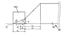
図9は、実際の発光位置と集束性レンズアレイ40の屈折率分布型レンズ42(図3ないし図5参照)との間に固体の光透過要素TR1と空気の層が存在する場合の光の進路の例を示す。次に、上述した式(2)の根拠をさらに詳細に説明する。
nb・sinθb≒sinθb=na・sinθa ...(9)
ここで、nbは空気の屈折率であり、θbは光透過要素TR1と空気の間の界面での空気への入射角、naは光透過要素TR1の屈折率であり、θaは光透過要素TR1と空気の間の界面での光透過要素TR1からの出射角である。na>nb≒1なので、θb>θaである。
tanθa=α/da ...(10)
tanθb=α/db ...(11)
ここで、daは光透過要素TR1の厚さ、dbは仮想的な発光位置上の点Pbから光透過要素TR1と空気の間の界面までの距離である。
db=da・cosθb/na・cosθa ...(12)
db=da/na ...(13)
nb・sinθb≒sinθb=na・sinθa=nd・sinθd ...(15)
ここで、nbは空気の屈折率であり、θbは光透過要素TR2がないと仮定した場合の空気と光透過要素TR1の間の界面での空気からの出射角(図10参照)、naは光透過要素TR1の屈折率であり、θaは光透過要素TR2がないと仮定した場合の空気と光透過要素TR1の間の界面での光透過要素TR1への入射角であり、光透過要素TR2がある場合の光透過要素TR2と光透過要素TR1の間の界面での光透過要素TR1への入射角である。na>nb≒1なので、θb>θaである。また、ndは光透過要素TR2の屈折率であり、θdは光透過要素TR2がある場合の光透過要素TR2と光透過要素TR1の間の界面での光透過要素TR2からの出射角である。nd>nb≒1なので、θb>θdである。さらに、図12(a)では、光透過要素TR1の屈折率naと光透過要素TR2の屈折率ndが互いに等しいので、θd=θaである。
tanθd=β/dd ...(16)
tanθb=β/dc ...(17)
ここで、ddは光透過要素TR2の厚さ、dcは仮想的な発光位置上の点Paから光透過要素TR2と光透過要素TR1の間の界面までの距離である。
dc=dd・cosθb/nd・cosθd ...(18)
dc=dd/nd ...(19)
L0=db+dc=da/na+dc=da/na+dd/nd ...(20)
L0=da/na+dd/nd=(da+dd)/na ...(24)
上述のように、発光パネル12と集束性レンズアレイ40との間に透明なスペーサ部材または透明な接着剤が介在する場合には、空気の層のみが介在する場合に比較して、発光パネル12上の像を集束性レンズアレイ40に対して焦点整合状態にするのに適切な発光パネル12と集束性レンズアレイ40との間隔が長くなる。別の見方をすると、発光パネル12と集束性レンズアレイ40との間隔が固定的に定まっていて(例えば図6のカバー13に発光パネル12と集束性レンズアレイ40があらかじめ固定されている場合など)、その間隔が集束性レンズアレイ40の発光パネル12側の空気中の実際の作動距離よりも長い場合には、適切な厚さのスペーサ部材または接着剤を両者の間に配置することにより、実質的に作動距離を伸ばして、発光パネル12と集束性レンズアレイ40との固定的な間隔に一致させることが可能である。
次に、上述した各種の電気光学装置の製造方法、特に透明な接着剤を必要箇所に適切な厚さで設ける方法を説明する。まず、発光パネル12と集束性レンズアレイ40を直接接合する第1の実施の形態の製造方法を説明する。図5に示すように、発光パネル12と集束性レンズアレイ40を極めて薄い接着剤38で接着する場合には、製造方法は単純であり、発光パネル12と集束性レンズアレイ40の少なくとも一方に接着剤38をコートして、他方をこれに接着すればよい。
上述したように、実施の形態の電気光学装置(例えば電気光学装置10,10A)は、電子写真方式を利用した画像印刷装置における像担持体に潜像を書き込むためのライン型の光ヘッドとして用いることが可能である。画像印刷装置の例としては、プリンタ、複写機の印刷部分およびファクシミリの印刷部分がある。
図46は、実施の形態の電気光学装置(例えば電気光学装置10,10A)のいずれかをライン型の光ヘッドとして用いた他の画像印刷装置の縦断面図である。この画像印刷装置は、ベルト中間転写体方式を利用したロータリ現像式のフルカラー画像印刷装置である。図46に示す画像印刷装置において、感光体ドラム(像担持体)165の周囲には、コロナ帯電器168、ロータリ式の現像ユニット161、有機ELアレイ露光ヘッド167、中間転写ベルト169が設けられている。
本発明に係る電気光学装置は、さらに各種の露光装置および照明装置に応用することが可能である。
Claims (3)
- 与えられた電気エネルギにより発光特性または光の透過特性が変化する複数の電気光学素子が配列された電気光学パネルと、
前記電気光学パネルから進行する光を透過させて前記電気光学パネル上の像に対する正立像を結像可能な屈折率分布型レンズが複数配列されて、複数の前記屈折率分布型レンズで得られた像が1つの連続した像を構成する集束性レンズアレイと、
前記電気光学パネルと前記集束性レンズアレイとの間に配置された透明なスペーサ部材とを備え、
前記スペーサ部材は前記集束性レンズアレイと透明な接着剤によって接合され、
前記スペーサ部材は前記電気光学パネルと透明な接着剤によって接合され、
前記集束性レンズアレイは、前記電気光学パネル側の作動距離と、前記電気光学パネルと反対側の作動距離とが等しく、
前記スペーサ部材には、前記電気光学パネルにも前記集束性レンズアレイにも対向しないすべての面に、前記スペーサ部材の内部を前記スペーサ部材の側面に向かって進む光を吸収する光吸収層が形成されており、前記光吸収層の屈折率が前記スペーサ部材の屈折率よりも高い、
ことを特徴とする電気光学装置。 - 前記電気光学パネルの電気光学素子と前記集束性レンズアレイの間にある光透過要素の各々の屈折率をni、前記光透過要素の各々の厚さをdi、前記光透過要素の数をm、前記集束性レンズアレイの電気光学パネル側の空気中の作動距離をL0としたとき、式(A)を満たすことを特徴とする請求項1に記載の電気光学装置。
- 像担持体と、
前記像担持体を帯電する帯電器と、
前記電気光学パネルから進行して前記集束性レンズアレイを透過する光を、前記像担持体の帯電された面に照射して潜像を形成する請求項1又は2に記載の電気光学装置と、
前記潜像にトナーを付着させることにより前記像担持体に顕像を形成する現像器と、
前記像担持体から前記顕像を他の物体に転写する転写器とを備える画像印刷装置。
Priority Applications (4)
| Application Number | Priority Date | Filing Date | Title |
|---|---|---|---|
| JP2005277268A JP4407601B2 (ja) | 2005-01-12 | 2005-09-26 | 電気光学装置および画像印刷装置 |
| US11/322,483 US7660022B2 (en) | 2005-01-12 | 2006-01-03 | Electro-optical device, image printing apparatus, and method of manufacturing electro-optical device |
| KR1020060002109A KR100743168B1 (ko) | 2005-01-12 | 2006-01-09 | 전기 광학 장치, 화상 인쇄 장치 및 전기 광학 장치의 제조방법 |
| TW095101055A TWI302124B (en) | 2005-01-12 | 2006-01-11 | Electro-optical device, image printing apparatus, and method of manufacturing electro-optical device |
Applications Claiming Priority (2)
| Application Number | Priority Date | Filing Date | Title |
|---|---|---|---|
| JP2005004843 | 2005-01-12 | ||
| JP2005277268A JP4407601B2 (ja) | 2005-01-12 | 2005-09-26 | 電気光学装置および画像印刷装置 |
Publications (2)
| Publication Number | Publication Date |
|---|---|
| JP2006218849A JP2006218849A (ja) | 2006-08-24 |
| JP4407601B2 true JP4407601B2 (ja) | 2010-02-03 |
Family
ID=36652872
Family Applications (1)
| Application Number | Title | Priority Date | Filing Date |
|---|---|---|---|
| JP2005277268A Expired - Fee Related JP4407601B2 (ja) | 2005-01-12 | 2005-09-26 | 電気光学装置および画像印刷装置 |
Country Status (4)
| Country | Link |
|---|---|
| US (1) | US7660022B2 (ja) |
| JP (1) | JP4407601B2 (ja) |
| KR (1) | KR100743168B1 (ja) |
| TW (1) | TWI302124B (ja) |
Families Citing this family (11)
| Publication number | Priority date | Publication date | Assignee | Title |
|---|---|---|---|---|
| JP2006218848A (ja) * | 2005-01-12 | 2006-08-24 | Seiko Epson Corp | 電気光学装置、画像印刷装置方法および電気光学装置の製造方法 |
| JP4912089B2 (ja) * | 2006-08-30 | 2012-04-04 | 京セラ株式会社 | 光プリンタヘッド |
| US9387688B2 (en) * | 2008-07-22 | 2016-07-12 | Brother Kogyo Kabushiki Kaisha | Exposure device and method for producing the same |
| JP5463894B2 (ja) * | 2009-12-15 | 2014-04-09 | セイコーエプソン株式会社 | 光源装置の製造方法 |
| CN102213932A (zh) * | 2010-04-01 | 2011-10-12 | 株式会社东芝 | 光学头、图像形成装置以及光学头的制造 |
| JP2011213085A (ja) | 2010-04-02 | 2011-10-27 | Fuji Xerox Co Ltd | 露光ヘッド及びその製造方法、カートリッジ、並びに画像形成装置 |
| JP5696379B2 (ja) * | 2010-06-23 | 2015-04-08 | 富士ゼロックス株式会社 | 結像ユニット。露光ヘッド及びその製造方法、カートリッジ、並びに画像形成装置 |
| JP5206753B2 (ja) * | 2010-09-01 | 2013-06-12 | 富士ゼロックス株式会社 | 露光装置及び画像形成装置 |
| JP6335456B2 (ja) * | 2012-10-05 | 2018-05-30 | キヤノン株式会社 | 露光装置および画像形成装置 |
| JP5212568B1 (ja) * | 2012-10-10 | 2013-06-19 | 富士ゼロックス株式会社 | 露光装置、画像形成装置 |
| JP6943225B2 (ja) * | 2018-06-22 | 2021-09-29 | 沖電気工業株式会社 | 露光ヘッド、画像形成装置、読取ヘッド及び読取装置 |
Family Cites Families (24)
| Publication number | Priority date | Publication date | Assignee | Title |
|---|---|---|---|---|
| JPS63103288A (ja) | 1986-10-21 | 1988-05-07 | オリンパス光学工業株式会社 | 端面発光el素子投影光学系 |
| GB2236818B (en) | 1989-09-14 | 1993-07-07 | Gen Motors France | Dual master cylinder |
| JPH03126003A (ja) | 1989-10-12 | 1991-05-29 | Toshiba Corp | 光学部品固定部構造 |
| JP2924110B2 (ja) | 1990-07-04 | 1999-07-26 | ミノルタ株式会社 | 光シャッタ装置 |
| JPH0530819A (ja) | 1991-07-29 | 1993-02-09 | Yanmar Agricult Equip Co Ltd | 水田用泥面検出装置 |
| JPH0538845A (ja) * | 1991-08-06 | 1993-02-19 | Eastman Kodak Japan Kk | 発光ダイオードアレイプリンタヘツド |
| US5902997A (en) * | 1994-05-20 | 1999-05-11 | Siemens Aktiengesellschaft | Device for spacing at least one lens from an optoelectronic component |
| US5655189A (en) * | 1994-05-27 | 1997-08-05 | Kyocera Corporation | Image device having thermally stable light emitting/receiving arrays and opposing lenses |
| JPH09293903A (ja) | 1996-04-30 | 1997-11-11 | Iwasaki Electric Co Ltd | 発光ダイオード配列体 |
| US6067106A (en) * | 1997-04-16 | 2000-05-23 | Canon Kabushiki Kaisha | Scanning optical apparatus |
| CA2240117A1 (en) * | 1997-07-23 | 1999-01-23 | Litton Systems, Inc. | Absorbing coating of optical media to prevent reflection, transmission and scatter |
| JP3702123B2 (ja) | 1999-04-27 | 2005-10-05 | 京セラ株式会社 | 光プリンタヘッド |
| JP2001010106A (ja) | 1999-07-02 | 2001-01-16 | Dainippon Screen Mfg Co Ltd | 記録ヘッド |
| JP2001026139A (ja) | 1999-07-15 | 2001-01-30 | Canon Inc | 露光装置及びそれを備える画像形成装置 |
| US6545819B1 (en) * | 1999-08-31 | 2003-04-08 | Canon Kabushiki Kaisha | Zoom lens and optical apparatus having the same |
| US6512219B1 (en) * | 2000-01-25 | 2003-01-28 | Amkor Technology, Inc. | Fabrication method for integrally connected image sensor packages having a window support in contact with the window and active area |
| CN100463484C (zh) | 2001-03-29 | 2009-02-18 | 松下电器产业株式会社 | 图像写入装置,光源,光源单元,微透镜以及微透镜的制造方法 |
| JP3708024B2 (ja) | 2001-03-29 | 2005-10-19 | 松下電器産業株式会社 | 画像書込み装置と画像書込み装置の光源 |
| JP2003025625A (ja) | 2001-07-16 | 2003-01-29 | Ricoh Co Ltd | 光プリントヘッドおよび画像形成装置 |
| JP3868780B2 (ja) | 2001-09-28 | 2007-01-17 | 日本板硝子株式会社 | 光書き込みヘッド |
| WO2003029011A1 (fr) | 2001-09-28 | 2003-04-10 | Nippon Sheet Glass Co.,Ltd. | Reseau de lentilles de resine et tete d'ecriture optique |
| JP2004058448A (ja) * | 2002-07-29 | 2004-02-26 | Denso Corp | 光プリンタヘッド |
| JP4089417B2 (ja) * | 2002-12-16 | 2008-05-28 | 富士ゼロックス株式会社 | 画像形成装置、および画像形成装置の制御方法 |
| JP2006218848A (ja) * | 2005-01-12 | 2006-08-24 | Seiko Epson Corp | 電気光学装置、画像印刷装置方法および電気光学装置の製造方法 |
-
2005
- 2005-09-26 JP JP2005277268A patent/JP4407601B2/ja not_active Expired - Fee Related
-
2006
- 2006-01-03 US US11/322,483 patent/US7660022B2/en not_active Expired - Fee Related
- 2006-01-09 KR KR1020060002109A patent/KR100743168B1/ko not_active IP Right Cessation
- 2006-01-11 TW TW095101055A patent/TWI302124B/zh not_active IP Right Cessation
Also Published As
| Publication number | Publication date |
|---|---|
| JP2006218849A (ja) | 2006-08-24 |
| US20060152653A1 (en) | 2006-07-13 |
| KR100743168B1 (ko) | 2007-07-27 |
| KR20060082403A (ko) | 2006-07-18 |
| TWI302124B (en) | 2008-10-21 |
| US7660022B2 (en) | 2010-02-09 |
| TW200631808A (en) | 2006-09-16 |
Similar Documents
| Publication | Publication Date | Title |
|---|---|---|
| KR100743168B1 (ko) | 전기 광학 장치, 화상 인쇄 장치 및 전기 광학 장치의 제조방법 | |
| KR100789871B1 (ko) | 전기 광학 장치, 화상 인쇄 장치 및 전기 광학 장치의 제조방법 | |
| US7697022B2 (en) | Electro-optical device and image forming apparatus | |
| JP2007190742A (ja) | 電気光学装置および画像印刷装置 | |
| CN100549855C (zh) | 电光学装置、图像打印装置以及电光学装置的制造方法 | |
| JP4353250B2 (ja) | 発光装置および画像印刷装置 | |
| CN101153696B (zh) | 电光装置、图像形成装置 | |
| JP4320681B2 (ja) | 電気光学装置および画像形成装置 | |
| JP2009099379A (ja) | 発光装置及び電子機器 | |
| JP4830332B2 (ja) | 電気光学装置、画像印刷装置および画像読み取り装置 | |
| JP4281795B2 (ja) | 電気光学装置、画像形成装置、および電気光学装置の製造方法 | |
| JP2008143025A (ja) | 電気光学装置、画像形成装置、および電気光学装置の製造方法 | |
| JP4617959B2 (ja) | 電気光学装置、画像印刷装置および画像読み取り装置 | |
| JP2011131457A (ja) | 光源装置および画像形成装置 | |
| JP4586560B2 (ja) | 画像印刷装置 | |
| JP2007090676A (ja) | 画像印刷装置ならびに画像印刷装置の調整方法および製造方法 | |
| JP2008149463A (ja) | 電気光学装置および画像形成装置 | |
| JP2007237575A (ja) | 電気光学装置、画像形成装置および電気光学装置の製造方法 | |
| JP2007253375A (ja) | 露光装置および画像形成装置 | |
| JP4367365B2 (ja) | 画像印刷装置 | |
| JP2007223298A (ja) | 電気光学装置および画像印刷装置 | |
| JP2007055106A (ja) | 露光装置および画像形成装置 | |
| JP2007276254A (ja) | 露光装置および画像形成装置 | |
| JP2007125841A (ja) | 露光装置および画像形成装置 | |
| JP2006264217A (ja) | 画像形成装置 |
Legal Events
| Date | Code | Title | Description |
|---|---|---|---|
| RD04 | Notification of resignation of power of attorney |
Free format text: JAPANESE INTERMEDIATE CODE: A7424 Effective date: 20070404 |
|
| A977 | Report on retrieval |
Free format text: JAPANESE INTERMEDIATE CODE: A971007 Effective date: 20081210 |
|
| A131 | Notification of reasons for refusal |
Free format text: JAPANESE INTERMEDIATE CODE: A131 Effective date: 20081216 |
|
| RD03 | Notification of appointment of power of attorney |
Free format text: JAPANESE INTERMEDIATE CODE: A7423 Effective date: 20090116 |
|
| A521 | Request for written amendment filed |
Free format text: JAPANESE INTERMEDIATE CODE: A523 Effective date: 20090213 |
|
| A02 | Decision of refusal |
Free format text: JAPANESE INTERMEDIATE CODE: A02 Effective date: 20090512 |
|
| A521 | Request for written amendment filed |
Free format text: JAPANESE INTERMEDIATE CODE: A523 Effective date: 20090811 |
|
| A911 | Transfer to examiner for re-examination before appeal (zenchi) |
Free format text: JAPANESE INTERMEDIATE CODE: A911 Effective date: 20090827 |
|
| TRDD | Decision of grant or rejection written | ||
| A01 | Written decision to grant a patent or to grant a registration (utility model) |
Free format text: JAPANESE INTERMEDIATE CODE: A01 Effective date: 20091020 |
|
| A01 | Written decision to grant a patent or to grant a registration (utility model) |
Free format text: JAPANESE INTERMEDIATE CODE: A01 |
|
| A61 | First payment of annual fees (during grant procedure) |
Free format text: JAPANESE INTERMEDIATE CODE: A61 Effective date: 20091102 |
|
| R150 | Certificate of patent or registration of utility model |
Free format text: JAPANESE INTERMEDIATE CODE: R150 |
|
| FPAY | Renewal fee payment (event date is renewal date of database) |
Free format text: PAYMENT UNTIL: 20121120 Year of fee payment: 3 |
|
| FPAY | Renewal fee payment (event date is renewal date of database) |
Free format text: PAYMENT UNTIL: 20121120 Year of fee payment: 3 |
|
| FPAY | Renewal fee payment (event date is renewal date of database) |
Free format text: PAYMENT UNTIL: 20131120 Year of fee payment: 4 |
|
| LAPS | Cancellation because of no payment of annual fees |