JP4342970B2 - Semiconductor memory device and manufacturing method thereof - Google Patents
Semiconductor memory device and manufacturing method thereof Download PDFInfo
- Publication number
- JP4342970B2 JP4342970B2 JP2004025935A JP2004025935A JP4342970B2 JP 4342970 B2 JP4342970 B2 JP 4342970B2 JP 2004025935 A JP2004025935 A JP 2004025935A JP 2004025935 A JP2004025935 A JP 2004025935A JP 4342970 B2 JP4342970 B2 JP 4342970B2
- Authority
- JP
- Japan
- Prior art keywords
- region
- conductivity type
- plug
- drain region
- emitter
- Prior art date
- Legal status (The legal status is an assumption and is not a legal conclusion. Google has not performed a legal analysis and makes no representation as to the accuracy of the status listed.)
- Expired - Fee Related
Links
- 239000004065 semiconductor Substances 0.000 title claims description 82
- 238000004519 manufacturing process Methods 0.000 title claims description 31
- 230000015654 memory Effects 0.000 claims description 142
- 239000010410 layer Substances 0.000 claims description 111
- 239000012535 impurity Substances 0.000 claims description 107
- 238000000034 method Methods 0.000 claims description 69
- 238000003860 storage Methods 0.000 claims description 45
- 239000000758 substrate Substances 0.000 claims description 44
- 239000011229 interlayer Substances 0.000 claims description 42
- 238000009792 diffusion process Methods 0.000 claims description 37
- 238000009825 accumulation Methods 0.000 claims description 9
- 239000013078 crystal Substances 0.000 claims description 4
- 108091006146 Channels Proteins 0.000 description 51
- 230000000052 comparative effect Effects 0.000 description 32
- VYPSYNLAJGMNEJ-UHFFFAOYSA-N Silicium dioxide Chemical compound O=[Si]=O VYPSYNLAJGMNEJ-UHFFFAOYSA-N 0.000 description 30
- 229910052814 silicon oxide Inorganic materials 0.000 description 30
- XUIMIQQOPSSXEZ-UHFFFAOYSA-N Silicon Chemical compound [Si] XUIMIQQOPSSXEZ-UHFFFAOYSA-N 0.000 description 29
- 229910052710 silicon Inorganic materials 0.000 description 28
- 239000010703 silicon Substances 0.000 description 28
- 238000010586 diagram Methods 0.000 description 20
- 229910021420 polycrystalline silicon Inorganic materials 0.000 description 17
- 229920005591 polysilicon Polymers 0.000 description 17
- 230000015572 biosynthetic process Effects 0.000 description 14
- 239000000969 carrier Substances 0.000 description 12
- 238000002955 isolation Methods 0.000 description 12
- 230000000694 effects Effects 0.000 description 11
- 238000001020 plasma etching Methods 0.000 description 10
- 230000006378 damage Effects 0.000 description 8
- 238000005229 chemical vapour deposition Methods 0.000 description 6
- 150000004767 nitrides Chemical class 0.000 description 6
- 230000002093 peripheral effect Effects 0.000 description 6
- 238000000206 photolithography Methods 0.000 description 6
- 108010075750 P-Type Calcium Channels Proteins 0.000 description 5
- 229910052581 Si3N4 Inorganic materials 0.000 description 5
- HQVNEWCFYHHQES-UHFFFAOYSA-N silicon nitride Chemical compound N12[Si]34N5[Si]62N3[Si]51N64 HQVNEWCFYHHQES-UHFFFAOYSA-N 0.000 description 5
- 238000005468 ion implantation Methods 0.000 description 3
- 238000004518 low pressure chemical vapour deposition Methods 0.000 description 3
- NBIIXXVUZAFLBC-UHFFFAOYSA-N Phosphoric acid Chemical compound OP(O)(O)=O NBIIXXVUZAFLBC-UHFFFAOYSA-N 0.000 description 2
- OAICVXFJPJFONN-UHFFFAOYSA-N Phosphorus Chemical group [P] OAICVXFJPJFONN-UHFFFAOYSA-N 0.000 description 2
- RTAQQCXQSZGOHL-UHFFFAOYSA-N Titanium Chemical compound [Ti] RTAQQCXQSZGOHL-UHFFFAOYSA-N 0.000 description 2
- 238000005530 etching Methods 0.000 description 2
- 238000010438 heat treatment Methods 0.000 description 2
- 230000003647 oxidation Effects 0.000 description 2
- 238000007254 oxidation reaction Methods 0.000 description 2
- 230000003071 parasitic effect Effects 0.000 description 2
- 229910052698 phosphorus Inorganic materials 0.000 description 2
- 239000011574 phosphorus Substances 0.000 description 2
- 229910052719 titanium Inorganic materials 0.000 description 2
- 239000010936 titanium Substances 0.000 description 2
- 229910021341 titanium silicide Inorganic materials 0.000 description 2
- 101100207343 Antirrhinum majus 1e20 gene Proteins 0.000 description 1
- ZOXJGFHDIHLPTG-UHFFFAOYSA-N Boron Chemical group [B] ZOXJGFHDIHLPTG-UHFFFAOYSA-N 0.000 description 1
- 229910000147 aluminium phosphate Inorganic materials 0.000 description 1
- 230000003321 amplification Effects 0.000 description 1
- 229910052796 boron Inorganic materials 0.000 description 1
- 239000003990 capacitor Substances 0.000 description 1
- 238000005516 engineering process Methods 0.000 description 1
- 230000010354 integration Effects 0.000 description 1
- 239000000463 material Substances 0.000 description 1
- 239000011159 matrix material Substances 0.000 description 1
- 229910021421 monocrystalline silicon Inorganic materials 0.000 description 1
- 238000003199 nucleic acid amplification method Methods 0.000 description 1
- 230000002265 prevention Effects 0.000 description 1
- 238000004544 sputter deposition Methods 0.000 description 1
Images


Classifications
-
- H—ELECTRICITY
- H10—SEMICONDUCTOR DEVICES; ELECTRIC SOLID-STATE DEVICES NOT OTHERWISE PROVIDED FOR
- H10D—INORGANIC ELECTRIC SEMICONDUCTOR DEVICES
- H10D30/00—Field-effect transistors [FET]
- H10D30/01—Manufacture or treatment
- H10D30/021—Manufacture or treatment of FETs having insulated gates [IGFET]
- H10D30/0411—Manufacture or treatment of FETs having insulated gates [IGFET] of FETs having floating gates
-
- G—PHYSICS
- G11—INFORMATION STORAGE
- G11C—STATIC STORES
- G11C16/00—Erasable programmable read-only memories
- G11C16/02—Erasable programmable read-only memories electrically programmable
- G11C16/06—Auxiliary circuits, e.g. for writing into memory
- G11C16/34—Determination of programming status, e.g. threshold voltage, overprogramming or underprogramming, retention
- G11C16/3418—Disturbance prevention or evaluation; Refreshing of disturbed memory data
- G11C16/3431—Circuits or methods to detect disturbed nonvolatile memory cells, e.g. which still read as programmed but with threshold less than the program verify threshold or read as erased but with threshold greater than the erase verify threshold, and to reverse the disturbance via a refreshing programming or erasing step
-
- H—ELECTRICITY
- H10—SEMICONDUCTOR DEVICES; ELECTRIC SOLID-STATE DEVICES NOT OTHERWISE PROVIDED FOR
- H10D—INORGANIC ELECTRIC SEMICONDUCTOR DEVICES
- H10D30/00—Field-effect transistors [FET]
- H10D30/60—Insulated-gate field-effect transistors [IGFET]
- H10D30/68—Floating-gate IGFETs
- H10D30/681—Floating-gate IGFETs having only two programming levels
-
- H—ELECTRICITY
- H10—SEMICONDUCTOR DEVICES; ELECTRIC SOLID-STATE DEVICES NOT OTHERWISE PROVIDED FOR
- H10D—INORGANIC ELECTRIC SEMICONDUCTOR DEVICES
- H10D30/00—Field-effect transistors [FET]
- H10D30/60—Insulated-gate field-effect transistors [IGFET]
- H10D30/711—Insulated-gate field-effect transistors [IGFET] having floating bodies
-
- H—ELECTRICITY
- H10—SEMICONDUCTOR DEVICES; ELECTRIC SOLID-STATE DEVICES NOT OTHERWISE PROVIDED FOR
- H10D—INORGANIC ELECTRIC SEMICONDUCTOR DEVICES
- H10D64/00—Electrodes of devices having potential barriers
- H10D64/01—Manufacture or treatment
- H10D64/031—Manufacture or treatment of data-storage electrodes
- H10D64/035—Manufacture or treatment of data-storage electrodes comprising conductor-insulator-conductor-insulator-semiconductor structures
-
- H—ELECTRICITY
- H10—SEMICONDUCTOR DEVICES; ELECTRIC SOLID-STATE DEVICES NOT OTHERWISE PROVIDED FOR
- H10D—INORGANIC ELECTRIC SEMICONDUCTOR DEVICES
- H10D86/00—Integrated devices formed in or on insulating or conducting substrates, e.g. formed in silicon-on-insulator [SOI] substrates or on stainless steel or glass substrates
- H10D86/01—Manufacture or treatment
-
- H—ELECTRICITY
- H10—SEMICONDUCTOR DEVICES; ELECTRIC SOLID-STATE DEVICES NOT OTHERWISE PROVIDED FOR
- H10D—INORGANIC ELECTRIC SEMICONDUCTOR DEVICES
- H10D86/00—Integrated devices formed in or on insulating or conducting substrates, e.g. formed in silicon-on-insulator [SOI] substrates or on stainless steel or glass substrates
- H10D86/201—Integrated devices formed in or on insulating or conducting substrates, e.g. formed in silicon-on-insulator [SOI] substrates or on stainless steel or glass substrates the substrates comprising an insulating layer on a semiconductor body, e.g. SOI
-
- G—PHYSICS
- G11—INFORMATION STORAGE
- G11C—STATIC STORES
- G11C16/00—Erasable programmable read-only memories
- G11C16/02—Erasable programmable read-only memories electrically programmable
- G11C16/04—Erasable programmable read-only memories electrically programmable using variable threshold transistors, e.g. FAMOS
Landscapes
- Semiconductor Memories (AREA)
- Dram (AREA)
Description
本発明は、半導体メモリ装置に係り、例えばSOI基板のような基板に形成されたトランジスタのチャネルボディの多数キャリア蓄積状態によりデータ記憶を行う半導体メモリ装置及びその製造方法に関する。 The present invention relates to a semiconductor memory device, and more particularly, to a semiconductor memory device that stores data by a majority carrier accumulation state of a channel body of a transistor formed on a substrate such as an SOI substrate, and a method of manufacturing the same.
最近、従来のDRAM代替を目的として、より単純なセル構造でダイナミック記憶を可能とした半導体メモリ装置が提案されている(特許文献1参照)。メモリセルは、SOI基板に形成されたフローティングのボディ(チャネルボディ)を持つ一つのトランジスタにより構成される。このメモリセルは、ボディに過剰の多数キャリアが蓄積された状態を第1データ状態(例えば、データ“1”)、ボディから過剰の多数キャリアが放出された状態を第2データ状態(例えば、データ“0”)として、二値記憶を行う。 Recently, for the purpose of replacing the conventional DRAM, a semiconductor memory device capable of dynamic storage with a simpler cell structure has been proposed (see Patent Document 1). The memory cell is composed of one transistor having a floating body (channel body) formed on an SOI substrate. In this memory cell, a state in which excessive majority carriers are accumulated in the body is a first data state (for example, data “1”), and a state in which excessive majority carriers are discharged from the body is a second data state (for example, data Binary storage is performed as “0”).
このようなメモリセルを“FBC(Floating Body Cell)”といい、FBCを用いた半導体メモリ装置を“FBCメモリ”という。FBCメモリは、通常のDRAMのようにキャパシタを用いないから、セルアレイの構造が単純であり、単位セル面積が小さく、従って高集積化が容易であるという長所を持つ。 Such a memory cell is called an “FBC (Floating Body Cell)”, and a semiconductor memory device using the FBC is called an “FBC memory”. Since an FBC memory does not use a capacitor as in a normal DRAM, the structure of the cell array is simple, the unit cell area is small, and thus high integration is easy.
FBCにおいても、DRAM等の他の半導体メモリと同様にデータの高速書込みやデータ破壊の防止が望まれる。 Also in the FBC, like other semiconductor memories such as DRAMs, it is desired to prevent high-speed data writing and data destruction.
本発明の目的は、データの高速書込みを可能にする半導体メモリ装置及びその製造方法を提供することである。 An object of the present invention is to provide a semiconductor memory device and a method for manufacturing the same that enable high-speed data writing.
本発明の他の目的は、データ破壊の防止を可能にする半導体メモリ装置及びその製造方法を提供することである。 Another object of the present invention is to provide a semiconductor memory device and a manufacturing method thereof that can prevent data destruction.
本発明に係る半導体メモリ装置の一態様は、基板と、絶縁層により前記基板と絶縁分離された第1導電型の半導体層と、ゲート電極と、前記半導体層に設けられた第2導電型のドレイン領域及びソース領域と、これらの領域の間の前記半導体層に設けられた第1導電型のチャネルボディと、を含むと共に前記チャネルボディの多数キャリア蓄積状態によりデータを記憶する記憶トランジスタと、前記ドレイン領域の上面と接する位置に設けられると共に前記ドレイン領域中の第2導電型の不純物濃度よりも第1導電型の不純物濃度が高く、前記ドレイン領域よりも浅く前記ドレイン領域に形成された第1導電型の不純物拡散領域と、前記不純物拡散領域をエミッタ領域、前記ドレイン領域をベース領域、前記チャネルボディをコレクタ領域とするバイポーラトランジスタであって前記記憶トランジスタにデータを書込むための書込トランジスタと、を備えることを特徴とする。 One embodiment of a semiconductor memory device according to the present invention includes a substrate, a first conductivity type semiconductor layer isolated from the substrate by an insulating layer, a gate electrode, and a second conductivity type provided in the semiconductor layer. A storage transistor including a drain region and a source region, and a first conductivity type channel body provided in the semiconductor layer between these regions, and storing data according to a majority carrier accumulation state of the channel body; top in contact with the impurity concentration of the first conductivity type than the impurity concentration of the second conductivity type in said drain region with is provided at a position of the drain region is rather high, the formed in the drain region shallower than said drain region An impurity diffusion region of one conductivity type, the impurity diffusion region as an emitter region, the drain region as a base region, and the channel body as a collector region. A write transistor for writing data to the storage transistor a bipolar transistor that is characterized in that it comprises.
本発明に係る半導体メモリ装置の他の態様は、基板と、絶縁層により前記基板と絶縁分離された第1導電型の半導体層と、ゲート電極と、前記半導体層に設けられた第2導電型の一対の不純物領域と、これらの領域の間の前記半導体層に設けられた第1導電型のチャネルボディと、を含むと共に前記チャネルボディの多数キャリア蓄積状態によりデータを記憶する複数の記憶トランジスタと、前記複数の記憶トランジスタを覆う層間絶縁膜と、前記複数の記憶トランジスタのうち前記一対の不純物領域の一方が隣り合っている記憶トランジスタどうしで共用すると共に前記層間絶縁膜に設けられこの膜から突き出して前記一対の不純物領域の一方に埋め込まれ、前記絶縁層まで達する導電性のプラグと、を備えることを特徴とする。 According to another aspect of the semiconductor memory device of the present invention, there is provided a substrate, a semiconductor layer of a first conductivity type insulated from the substrate by an insulating layer, a gate electrode, and a second conductivity type provided in the semiconductor layer. A plurality of storage transistors for storing data in accordance with a majority carrier accumulation state of the channel body, and a first conductivity type channel body provided in the semiconductor layer between the regions. And an interlayer insulating film covering the plurality of memory transistors, and one of the pair of impurity regions among the plurality of memory transistors being shared by adjacent memory transistors and protruding from the film provided in the interlayer insulating film And a conductive plug embedded in one of the pair of impurity regions and reaching the insulating layer .
本発明に係る半導体メモリ装置の製造方法の一態様は、ゲート電極と、絶縁層により基板と絶縁分離された第1導電型の半導体層に設けられた第2導電型のドレイン領域及びソース領域と、これらの領域の間の前記半導体層に設けられた第1導電型のチャネルボディと、を含む記憶トランジスタを形成する工程と、前記記憶トランジスタを覆う層間絶縁膜を形成する工程と、前記ドレイン領域を露出するエミッタ用コンタクトホールを前記層間絶縁膜に形成する工程と、前記エミッタ用コンタクトホールに第1導電型のエミッタプラグを形成する工程と、前記エミッタプラグ中の第1導電型の不純物を前記ドレイン領域の上面に熱拡散して前記ドレイン領域の上面に、前記ドレイン領域中の第2導電型の不純物濃度よりも第1導電型の不純物濃度が高く、前記ドレイン領域よりも浅く前記ドレイン領域に形成された第1導電型のエミッタ領域を形成する工程と、を備えることを特徴とする。 One aspect of a method for manufacturing a semiconductor memory device according to the present invention includes: a gate electrode; a drain region and a source region of a second conductivity type provided in a semiconductor layer of a first conductivity type that is insulated from the substrate by an insulating layer; A step of forming a storage transistor including a first conductivity type channel body provided in the semiconductor layer between these regions, a step of forming an interlayer insulating film covering the storage transistor, and the drain region Forming a contact hole for emitter exposing the interlayer insulating film, a step of forming an emitter plug of a first conductivity type in the contact hole for emitter, and an impurity of the first conductivity type in the emitter plug An impurity of the first conductivity type is formed on the upper surface of the drain region by thermal diffusion to the upper surface of the drain region, compared with the impurity concentration of the second conductivity type in the drain region. Degree is rather high, characterized in that it comprises the steps of forming the emitter region of the first conductivity type formed in the drain region shallower than said drain region.
本発明に係る半導体メモリ装置の製造方法のさらに他の態様は、ゲート電極と、絶縁層により基板と絶縁分離された第1導電型の半導体層に設けられた第2導電型の一対の不純物領域と、これらの領域の間の前記半導体層に設けられた第1導電型のチャネルボディと、を含む複数の記憶トランジスタが、隣り合うものどうしで前記一対の不純物領域の一方を共用するように形成する工程と、前記複数の記憶トランジスタを覆う層間絶縁膜を形成する工程と、前記一対の不純物領域を貫通して前記絶縁層まで達するコンタクトホールを前記層間絶縁膜に形成する工程と、前記コンタクトホールに、前記一対の不純物領域の一方の内部にまで入り込み、前記絶縁層に到達すると共に隣り合う記憶トランジスタどうしで共用する導電性のプラグを形成する工程と、を備えることを特徴とする。 According to still another aspect of the method for manufacturing a semiconductor memory device of the present invention, a pair of impurity regions of a second conductivity type provided in a gate electrode and a semiconductor layer of the first conductivity type isolated from the substrate by an insulating layer. And a plurality of memory transistors including a first conductivity type channel body provided in the semiconductor layer between these regions are formed so that adjacent ones share one of the pair of impurity regions. A step of forming an interlayer insulating film covering the plurality of storage transistors, a step of forming a contact hole through the pair of impurity regions and reaching the insulating layer in the interlayer insulating film, and the contact hole to, one of the viewing write enters into the inside, form a conductive plug to be shared by the memory transistor to each other adjacent both upon reaching the insulating layer of the pair of impurity regions Characterized in that it comprises the steps of, a.
本発明の一局面によれば、データの高速書込みが可能な半導体メモリ装置及びその製造方法を実現することができる。また、本発明の他の局面によれば、データ破壊の防止が可能な半導体メモリ装置及びその製造方法を実現することができる。 According to one aspect of the present invention, a semiconductor memory device capable of high-speed data writing and a method for manufacturing the same can be realized. According to another aspect of the present invention, a semiconductor memory device capable of preventing data destruction and a method for manufacturing the same can be realized.
本発明の実施形態を以下の項目に分けて説明する。メモリセルはFBCを意味する。
[第1実施形態]
(第1比較例)
(第2比較例)
(第1実施形態に係るメモリセルの構造)
(第1実施形態の主な効果)
(第1実施形態に係るメモリセルの製造方法)
(第1実施形態に係るセルアレイ)
[第2実施形態]
[第3実施形態]
[第4実施形態]
[第5実施形態]
(第5実施形態に係るメモリセルの構造)
(第5実施形態の主な効果)
(第5実施形態に係るメモリセル製造方法)
[第6実施形態]
[第7実施形態]
なお、各実施形態を説明する図において、既に説明した図の符号で示すものと同一のものについては、同一符号を付すことにより説明を省略する。
The embodiment of the present invention will be described by dividing it into the following items. A memory cell means FBC.
[First Embodiment]
(First comparative example)
(Second comparative example)
(Structure of Memory Cell According to First Embodiment)
(Main effects of the first embodiment)
(Method for Manufacturing Memory Cell According to First Embodiment)
(Cell array according to the first embodiment)
[Second Embodiment]
[Third Embodiment]
[Fourth Embodiment]
[Fifth Embodiment]
(Structure of Memory Cell According to Fifth Embodiment)
(Main effects of the fifth embodiment)
(Memory Cell Manufacturing Method According to Fifth Embodiment)
[Sixth Embodiment]
[Seventh Embodiment]
Note that, in the drawings for explaining the embodiments, the same components as those shown in the drawings already described are denoted by the same reference numerals, and the description thereof is omitted.
[第1実施形態]
第1実施形態に係るメモリセルを説明する前に、この理解のために、まず、第1及び第2比較例から説明する。
[First Embodiment]
Before describing the memory cell according to the first embodiment, first, for the sake of understanding, the first and second comparative examples will be described.
(第1比較例)
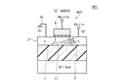
図1は、第1比較例に係るメモリセルの断面の模式図である。メモリセルMCは、一つの記憶トランジスタMTrから構成されている。記憶トランジスタMTrは、SOI基板1に形成されている。記憶トランジスタMTrは、SOI基板1のp型の半導体層3に設けられたn型のドレイン領域5及びソース領域7と、半導体層3の上にゲート絶縁膜を介して配置されたゲート電極9と、を備える。ドレイン領域5とソース領域7の間であってゲート電極9直下の半導体層3には、p型のチャネルボディ11が形成されている。チャネルボディ11は、フローティングボディとなる。ゲート電極9はワード線WLに接続され、ドレイン領域5はビット線BLに接続され、ソース領域7はソース線SLに接続されている。ソース線SLは接地されている。
(First comparative example)
FIG. 1 is a schematic cross-sectional view of a memory cell according to a first comparative example. The memory cell MC is composed of one storage transistor MTr. The storage transistor MTr is formed on the
メモリセルMCの動作について図1〜図3で説明する。図2及び図3で示す断面の構造は図1のそれと同じである。図1はデータ“1”の書込み動作、図2はデータ“0”の書込み動作、図3はデータの読出し動作を示している。 The operation of the memory cell MC will be described with reference to FIGS. The structure of the cross section shown in FIGS. 2 and 3 is the same as that of FIG. 1 shows a data “1” write operation, FIG. 2 shows a data “0” write operation, and FIG. 3 shows a data read operation.
図1に示すように、メモリセルMCへのデータ“1”の書込みには、メモリセルMCに大きなチャネル電流が流れるバイアス条件を与える。例えば、ワード線WLに1.5V、ビット線BLに1.5Vを印加する。これにより、ドレイン領域5近傍でインパクトイオン化により発生する多数キャリア(図の例ではホールhole)をチャネルボディ11に蓄積する。
As shown in FIG. 1, when data “1” is written to the memory cell MC, a bias condition for allowing a large channel current to flow through the memory cell MC is given. For example, 1.5V is applied to the word line WL and 1.5V is applied to the bit line BL. As a result, majority carriers (holes in the example in the figure) generated by impact ionization in the vicinity of the
一方、データ“0”書込みは、図2に示すように、例えばワード線WLに1.5V、ビット線BLに−1Vを印加する。これにより、ドレイン領域5とチャネルボディ11の間のPN接合を順バイアス状態として、ボディ11の多数キャリアをドレイン領域5側に放出させる。
On the other hand, for writing data “0”, as shown in FIG. 2, for example, 1.5V is applied to the word line WL and −1V is applied to the bit line BL. As a result, the PN junction between the
ボディ11のキャリア蓄積状態の相違は、記憶トランジスタMTrのしきい値の相違として現れる。従って、図3に示すように、例えばワード線WLに1.5V、ビット線BLに0.2Vを与えて、セル電流の有無又は大小を検出することにより、データ“0”,“1”の読出しができる。
The difference in the carrier accumulation state of the
図4は、記憶トランジスタMTrのドレイン電流Ids−ゲート電圧Vgs特性をデータ“0”,“1”について示している。なお、チャネルボディ11の過剰の多数キャリアは、長時間放置すると、ドレイン領域5、ソース領域7との間のPN接合を介して抜ける。従って、DRAMと同様に一定周期でリフレッシュ動作を行うことが必要である。
FIG. 4 shows the drain current Ids-gate voltage Vgs characteristics of the storage transistor MTr for data “0” and “1”. If excessive majority carriers in the
(第2比較例)
図5は、第2比較例に係るメモリセルMCの断面の模式図である。図6はその等価回路を示している。このメモリセルMCは、図1の記憶トランジスタMTrに、データ書込み用の書込トランジスタWTrを加えた構成をしている。トランジスタWTrは、寄生PNPバイポーラトランジスタである。詳しくは、トランジスタWTrのp型のエミッタ領域13は、この領域とp型のチャネルボディ11との間にn型のドレイン領域5が位置するように、半導体層3に設けられている。トランジスタWTrは、ドレイン領域5をn型のベース領域、チャネルボディ11をp型のコレクタ領域としている。
(Second comparative example)
FIG. 5 is a schematic diagram of a cross section of the memory cell MC according to the second comparative example. FIG. 6 shows an equivalent circuit thereof. The memory cell MC has a configuration in which a write transistor WTr for data writing is added to the storage transistor MTr of FIG. The transistor WTr is a parasitic PNP bipolar transistor. Specifically, the p-
メモリセルMCのゲート電極9はワード線WLに接続され、ドレイン領域5はワード線WLと交差するビット線BLに接続され、ソース領域7はソース線SLに接続される。エミッタ領域13は、ワード線WLと並行するエミッタ線ELに接続される。
第2比較例に係るメモリセルMCは、第1比較例と同様に、記憶トランジスタMTrのチャネルボディ11が過剰の多数キャリア(ホール)を保持する第1データ状態(“1”データ)と、それより過剰のホールが少ない第2データ状態(“0”データ)を、ダイナミックに記憶する。図5には、メモリセルMCに“1”書込みを行う場合のバイアス例を示している。“1”書込み時、ワード線WLに−1.5V、ビット線BLに−1V、エミッタ線ELに0Vが与えられる。ソース線SLは0Vである。
As in the first comparative example, the memory cell MC according to the second comparative example has the first data state (“1” data) in which the
このとき、p型のエミッタ領域13とn型のドレイン領域5との間のPN接合(トランジスタWTrのベース・エミッタ接合)が順バイアスになり、エミッタ領域13からドレイン領域5にホールholeが注入される。注入されたホールは、一部がドレイン領域5で再結合し、残りがp型のチャネルボディ11に到達する。言い換えれば、“1”書込みは、書込トランジスタWTrであるバイポーラトランジスタのオン動作により、記憶トランジスタMTrのチャネルボディ11にホールを注入する動作となる。以下、この書込みを“バイポーラ書込み”という。
At this time, the PN junction (base-emitter junction of the transistor WTr) between the p-
バイポーラ書込みでは、エミッタ線ELとビット線BL間の電圧を調整することにより、チャネルボディ11に流れ込む電流(コレクタ電流)を容易に増やすことができる。このため、高速の“1”書込みが可能になる。
In bipolar writing, the current (collector current) flowing into the
“0”書込みは、第1比較例と同様である。ワード線WLに例えば1.5Vを与えて、チャネルボディ11の電位を上げ、ビット線BLには例えば−2Vを与える。書込トランジスタWTrはオフを保つ。これにより、チャネルボディ11とドレイン領域5の間が順方向バイアスされ、チャネルボディ11のホールがドレイン領域5に放出されて、過剰ホールの少ない“0”データが書かれる。第2比較例のメモリセルMCも、“0”又は“1”データをダイナミックに記憶するから、一定周期でのデータリフレッシュが必要である。
“0” writing is the same as in the first comparative example. For example, 1.5V is applied to the word line WL to raise the potential of the
(第1実施形態に係るメモリセルの構造)
第1実施形態に係るメモリセルは、第2比較例と同様の書込み動作であるが、エミッタ領域の不純物濃度を第2比較例よりも高くできるため、書込みをさらに高速化できる。図7は、第1実施形態に係るメモリセルの概要を示す模式図である。このメモリセルMCは、第2比較例と同様に一組の記憶トランジスタMTrと書込トランジスタWTrにより構成される。
(Structure of Memory Cell According to First Embodiment)
The memory cell according to the first embodiment has the same write operation as that of the second comparative example. However, since the impurity concentration of the emitter region can be made higher than that of the second comparative example, the writing can be further speeded up. FIG. 7 is a schematic diagram showing an outline of the memory cell according to the first embodiment. Similar to the second comparative example, the memory cell MC includes a pair of a memory transistor MTr and a write transistor WTr.
記憶トランジスタMTrは、フローティングボディを持つNMOSトランジスタである。書込トランジスタWTrは、そのフローティングボディをコレクタとするバイポーラトランジスタである。これらのトランジスタは、シリコン基板21(基板の一例)、シリコン酸化層23(絶縁層の一例)、単結晶のp型のシリコン層25(第1導電型の半導体層の一例)が積層された構造を有するSOI基板27に形成されている。シリコン層25は、シリコン酸化層23によりシリコン基板21と絶縁分離されている。シリコン層25を囲むように素子分離絶縁膜29が形成されている。
The memory transistor MTr is an NMOS transistor having a floating body. Write transistor WTr is a bipolar transistor whose collector is the floating body. These transistors have a structure in which a silicon substrate 21 (an example of a substrate), a silicon oxide layer 23 (an example of an insulating layer), and a single crystal p-type silicon layer 25 (an example of a first conductivity type semiconductor layer) are stacked. Is formed on an
記憶トランジスタMTrは、シリコン層25にゲート絶縁膜31を介して配置されたゲート電極33と、これと自己整合的にシリコン層25に形成されたn型(第2導電型の一例)のドレイン領域35及びソース領域37と、を備える。これらの領域の間であってゲート電極33直下のシリコン層25には、p型のチャネルボディ39が形成されている。チャネルボディ39は、フローティングボディとなる。記憶トランジスタMTrは、第1及び第2比較例と同様に、チャネルボディ39の多数キャリア蓄積状態によりデータを記憶する。詳しくは、チャネルボディ39が過剰の多数キャリアを保持する第1データ状態と、チャネルボディ39が第1データ状態より少ない多数キャリアを保持する第2データ状態とのいずれかを記憶する。
The memory transistor MTr includes a
ドレイン領域35のゲート電極33側の上面と接する位置には、p型(第1導電型の一例)の不純物拡散領域41が設けられている。詳しくは、不純物拡散領域41は、ドレイン領域35よりも浅くドレイン領域35に形成されている。書込トランジスタWTrは、p型の不純物拡散領域41をエミッタ領域、n型のドレイン領域35をベース領域、p型のチャネルボディ39をコレクタ領域とするPNPバイポーラトランジスタであり、記憶トランジスタMTrへのデータの書込みに利用される。
A p-type (an example of a first conductivity type)
不純物拡散領域41(エミッタ領域)は、ドレイン領域35(ベース領域)よりも浅い。具体的には、不純物拡散領域41の深さは20〜30nmであり、ドレイン領域35の深さは50〜150nmである。また、不純物拡散領域41(エミッタ領域)のp型の不純物濃度は、ドレイン領域35(ベース領域)のn型の不純物濃度1×10¹⁹/cm3より大きく、例えば、1×1020〜1×1021/cm3である。
The impurity diffusion region 41 (emitter region) is shallower than the drain region 35 (base region). Specifically, the depth of the
ドレイン領域35のうち素子分離絶縁膜29と不純物拡散領域41との間には、この領域35と接続する導電性のドレインプラグ43(コンタクトプラグ)が設けられている。このプラグ43は、n型の不純物を含むポリシリコンで構成される。
In the
不純物拡散領域41(エミッタ領域)上には、この領域41と接続する導電性のエミッタプラグ45が形成されている。エミッタプラグ45は、p型の不純物を含むポリシリコンであり、この不純物をドレイン領域35に拡散することにより、不純物拡散領域41が形成される。
On the impurity diffusion region 41 (emitter region), a conductive emitter plug 45 connected to the
また、ソース領域37上には、この領域37と接続する導電性のソースプラグ47が設けられている。プラグ47はn型のポリシリコンである。ソースプラグ47、ゲート電極33、エミッタプラグ45、ドレインプラグ43の順に並んでいる。
Further, a conductive source plug 47 connected to the
なお、SOI基板27には、複数のメモリセルMCがアレイ状に配置されたセルアレイが配置されている(セルアレイの構造は後で説明する)。このSOI基板27には、ビット線セレクタのようなセルアレイの周辺回路も形成されている。これを示すのが図8の断面図である。メモリセルMCの断面は図7と同様である。SOI基板27の周辺回路領域には、周辺回路の構成要素となるNMOSトランジスタQが表れている。
Note that a cell array in which a plurality of memory cells MC are arranged in an array is arranged on the SOI substrate 27 (the structure of the cell array will be described later). On the
(第1実施形態の主な効果)
第1実施形態の主な効果を第2比較例と比較しながら説明する。図9は、第2比較例に係るメモリセルの主要部の模式図であり、図7と対応する。図9が図7と相違する主な点は次ぎの通りである。素子分離絶縁膜29とドレイン領域35の間のp型のシリコン層25がエミッタ領域49にされている。エミッタ領域49のp型の不純物濃度は、1×10¹⁷/cm3である。また、ドレインプラグ43とエミッタプラグ45の順番が入れ替わっている。
(Main effects of the first embodiment)
The main effects of the first embodiment will be described in comparison with the second comparative example. FIG. 9 is a schematic diagram of the main part of the memory cell according to the second comparative example, and corresponds to FIG. The main points in which FIG. 9 is different from FIG. 7 are as follows. A p-
さて、エミッタ領域を高濃度化すれば、hFE(hFE;パイポーラトランジスタの電流増幅率)が大きくなるため、書込み電流が大きくなり、その結果、バイポーラ書込みをさらに高速化できる。しかし、図9の第2比較例では、エミッタ領域49のp型不純物濃度をドレイン領域35のn型不純物濃度よりも高くできない。この理由を説明する。
By increasing the concentration of the emitter region, hFE (hFE; current amplification factor of the bipolar transistor) increases, so that the write current increases, and as a result, the speed of bipolar writing can be further increased. However, in the second comparative example of FIG. 9, the p-type impurity concentration of the
第2比較例では、エミッタ領域49がドレイン領域35(ベース領域)とドレイン領域35の側面48で接合する構造なので、p型のシリコン層25をエミッタ領域49にしている。記憶トランジスタMTrは、p型のシリコン層25にn型のドレイン領域35及びソース領域37を形成したNMOS構造である。このNMOSが動作するためには、シリコン層25のp型不純物濃度がドレイン領域35及びソース領域37のn型不純物濃度より低くなければならない。例えば、ドレイン領域35及びソース領域37のn型不純物濃度が1×10¹⁹/cm3の場合、シリコン層25のp型不純物濃度は1×1017/cm3となるので、エミッタ領域49のp型不純物濃度は1×1017/cm3となる。よって、第2比較例では、エミッタ領域49のp型不純物濃度がドレイン領域35(ベース領域)のn型不純物濃度より低くなるので、書込トランジスタWTrのhFEは1以下となり、通常のバイポーラトランジスタより小さくなる。
In the second comparative example, since the
これに対して、図7に示す第1実施形態では、ドレイン領域35の上面と接する位置にエミッタ領域となるp型の不純物拡散領域41を設けている。このため、第2比較例のような制約はなく、不純物拡散領域41のp型不純物濃度をドレイン領域35のn型不純物濃度よりも高くできる。したがって、書込トランジスタWTrのhFEを1より大きくでき、書込みのさらなる高速化が可能となる。例えば、第1実施形態では第2比較例よりも、エミッタ領域のp型不純物濃度が二桁以上高くなり、これによりエミッタ電流も二桁以上高くなるため、記憶トランジスタMTrへの高速書込みが可能となる。
On the other hand, in the first embodiment shown in FIG. 7, a p-type
なお、不純物拡散領域41をゲート電極33側ではなく、素子分離絶縁膜29側に配置し、これに伴いエミッタプラグ45を外側に配置し、ドレインプラグ43をエミッタプラグ45とゲート電極33の間に配置した構造でも、上記の効果を得ることができる。
The
(第1実施形態に係るメモリセルの製造方法)
第1実施形態に係るメモリセルの製造方法について、図10〜図22を用いて説明する。図10〜図22は、この製造方法を工程順に示すSOI基板等の断面図である。まず、図10に示すように、SOI基板27を準備する。SOI基板27は、支持基板となるシリコン基板21、埋め込み酸化膜となるシリコン酸化層23、p型のシリコン層25が積層された構造を有する。シリコン層25のp型の不純物濃度は比較的低くされている(1×10¹⁴/cm3)。
(Method for Manufacturing Memory Cell According to First Embodiment)
A method for manufacturing a memory cell according to the first embodiment will be described with reference to FIGS. 10 to 22 are sectional views of an SOI substrate and the like showing this manufacturing method in the order of steps. First, as shown in FIG. 10, an
図11に示すように、フォトリソグラフィと反応性イオンエッチングにより、シリコン層25の素子形成領域51以外の領域を除去してトレンチ53を形成する。トレンチ53に、STI(Shallow Trench Isolation)技術により素子分離絶縁膜29を形成する。次に、シリコン層25の全面にやや高濃度のp型の不純物をイオン注入することにより、素子形成領域51をチャネル領域にする。このときの素子形成領域51の不純物濃度は、1×10¹⁸/cm3である。このイオン注入の条件は、例えば、p型の不純物がホウ素であり、ドーズ量が1×1013/cm2〜1.5×1013/cm2である。
As shown in FIG. 11,
図12に示すように、シリコン層25の全面に熱酸化により、ゲート絶縁膜となる薄い絶縁膜を形成する。その上に厚さ300nm程度のポリシリコン膜をCVD(Chemical Vapor Deposition)により形成する。上記ポリシリコン膜と薄い絶縁膜をフォトリソグラフィと反応性イオンエッチングによりパターニングして、素子形成領域51にゲート電極33、ゲート絶縁膜31を形成する。
As shown in FIG. 12, a thin insulating film to be a gate insulating film is formed on the entire surface of the
図13に示すように、ゲート電極33をマスクとしてn型の不純物を素子形成領域51にイオン注入して、LDD領域であるn型低濃度領域57を形成する。このイオン注入の条件は、例えば、n型の不純物がリンであり、ドーズ量が1×10¹³/cm2程度である。そして、シリコン層25の全面にCVDにより、シリコン窒化膜を形成する。この窒化膜を反応性イオンエッチングによりエッチングすることにより、ゲート電極33の側面に側壁窒化膜55を形成する。ゲート電極33及び側壁窒化膜55をマスクとしてn型の不純物を素子形成領域51にイオン注入して、n型高濃度領域59を形成する。このイオン注入の条件は、例えば、n型の不純物がリンであり、ドーズ量が1×1013/cm2〜2×1013/cm2である。n型低濃度領域57とn型高濃度領域59により、LDD構造のドレイン領域35、ソース領域37が構成される。これらの領域35,37のn型不純物濃度は、1×1019/cm3である。以上により、ゲート電極33、ドレイン領域35、ソース領域37及びチャネルボディ39を含む記憶トランジスタMTrが形成される。
As shown in FIG. 13, n-type impurities are ion-implanted into the
図14に示すように、側壁窒化膜55をエッチング(例えば加熱燐酸)により除去する。側壁窒化膜55は周辺回路のMOSトランジスタ用であり、記憶トランジスタMTr用の側壁酸化膜は後の工程で形成される。
As shown in FIG. 14, the
図15に示すように、シリコン層25の全面に、LPCVD(Low Pressure Chemical Vapor Deposition)により、順に、シリコン酸化膜61、シリコン窒化膜63、比較的厚め(300nm)のシリコン酸化膜65を形成する。これらが記憶トランジスタMTrを覆う層間絶縁膜67となる。そして、ゲート電極33上のシリコン窒化膜63が露出するまで、シリコン酸化膜65を研磨して、シリコン酸化膜65を平坦化する。
As shown in FIG. 15, a
図16に示すように、層間絶縁膜67に、フォトリソグラフィと反応性イオンエッチングにより、ドレイン領域35を露出するドレイン用コンタクトホール69、ソース領域37を露出するソース用コンタクトホール71を形成する。
As shown in FIG. 16, a
図17に示すように、厚さ400nmのn型のポリシリコン膜を、コンタクトホール69,71が埋まるように、層間絶縁膜67の全面にCVDにより形成する。そして、このポリシリコン膜がコンタクトホール69,71に残るように、このポリシリコン膜を反応性イオンエッチングする。これにより、ドレイン用コンタクトホール69にドレインプラグ43、ソース用コンタクトホール71にソースプラグ47を形成する。
As shown in FIG. 17, an n-type polysilicon film having a thickness of 400 nm is formed by CVD on the entire surface of the
図18に示すように、フォトリソグラフィと反応性イオンエッチングにより、ドレインプラグ43とゲート電極33との間の層間絶縁膜67に、ドレイン領域35を露出するエミッタ用コンタクトホール73を形成する。
As shown in FIG. 18, an
図19に示すように、コンタクトホール73が埋まるように、エミッタプラグとなる厚さ400nmのp型のポリシリコン膜を、CVDにより層間絶縁膜67の全面に形成する。このポリシリコン膜のp型の不純物濃度は、1e20/cm3程度である。そして、このポリシリコン膜がコンタクトホール73に残るように、このポリシリコン膜を反応性イオンエッチングする。これにより、エミッタ用コンタクトホール73にエミッタプラグ45を形成する。
As shown in FIG. 19, a p-type polysilicon film having a thickness of 400 nm serving as an emitter plug is formed on the entire surface of the
図20に示す構造体を熱処理する。条件は、温度1015℃であり、時間10秒である。この熱処理で、ドレイン領域35、ソース領域37のn型の不純物を活性化させる。また、この熱処理により、p型のエミッタプラグ45からドレイン領域35の上面50(表面)にp型の不純物が拡散して、ドレイン領域35の上面50に、この領域35中のn型不純物濃度よりもp型不純物濃度が高いp型の不純物拡散領域41(エミッタ領域)が形成される。これにより、不純物拡散領域41をエミッタ領域、ドレイン領域35をベース領域、チャネルボディ39をコレクタ領域とするバイポーラトランジスタである書込トランジスタWTrが形成される。
The structure shown in FIG. 20 is heat-treated. The conditions are a temperature of 1015 ° C. and a time of 10 seconds. By this heat treatment, the n-type impurities in the
図21に示すように、露出しているシリコン窒化膜63、その下のシリコン酸化膜61を反応性イオンエッチングで除去して、ゲート電極33の上面を露出させる。そして、層間絶縁膜67の全面にスパッタリングによりチタン膜を形成する。図21に示す構造体を熱処理することにより、このチタン膜を、ゲート電極33、ドレインプラグ43、エミッタプラグ45及びソースプラグ47中のシリコンと反応させる。これにより、ゲート電極33、ドレインプラグ43、エミッタプラグ45及びソースプラグ47の上面にチタンシリサイド膜75を形成する。
As shown in FIG. 21, the exposed
図22に示すように、層間絶縁膜67の上にLPCVDにより、層間絶縁膜となる厚さ600nmのシリコン酸化膜77を形成する。その後、図示はしないがシリコン酸化膜77にプラグが形成される。これにより、ドレインプラグ43をビット線BLに、エミッタプラグ45をエミッタ線ELに、ソースプラグ47をソース線SLに、それぞれ接続する。以上の工程により、第1実施形態に係るメモリセルを作製することができる。
As shown in FIG. 22, a 600 nm thick
なお、図18及び図19に示すように、エミッタ用コンタクトホール73をドレイン用コンタクトホール69よりもゲート電極33側に位置するように形成することにより、エミッタプラグ45をドレインプラグ43よりもゲート電極33側に形成している。しかしながら、逆にしてもよい。つまり、ドレイン用コンタクトホール69をエミッタ用コンタクトホール73よりもゲート電極33側に位置するように形成して、ドレインプラグ43をエミッタプラグ45よりもゲート電極33側に形成する。
As shown in FIGS. 18 and 19, the
また、ドレインプラグ43及びソースプラグ47の形成後に、エミッタプラグ45を形成している。しかしながら、この逆でもよい。
In addition, the
(第1実施形態に係るセルアレイ)
図23は、第1実施形態に係るセルアレイの一部のレイアウトを示す平面図である。図24は、図23のA1−A2断面の模式図である。図23及び図24を用いてセルアレイの構造を説明する。ソース線SL、ワード線WL、エミッタ線ELが同一の方向に延びている。ソース線SLはソースプラグ47、エミッタ線ELはエミッタプラグ45に接続されている。ビット線BLは、これらの線と直交する方向に延びており、ドレインプラグ43と接続されている。セルアレイは、複数のメモリセルMCがアレイ状に配置された構造を有する。詳しくは、複数のメモリセルMCがビット線BLとワード線WLが交差する位置にマトリクス配列されている。
(Cell array according to the first embodiment)
FIG. 23 is a plan view showing a layout of part of the cell array according to the first embodiment. FIG. 24 is a schematic diagram of the A1-A2 cross section of FIG. The structure of the cell array will be described with reference to FIGS. The source line SL, word line WL, and emitter line EL extend in the same direction. The source line SL is connected to the source plug 47, and the emitter line EL is connected to the
図24には隣り合う二つのメモリセルMC1,MC2が表れている。メモリセルMC1の断面は図7に示すメモリセルMCの断面と同じである。メモリセルMC2の断面は、メモリセルMC1とメモリセルMC2の間にある素子分離絶縁膜29を中心として、メモリセルMC1の断面を折り返した構造になっている。つまり、メモリセルMC1の断面とメモリセルMC2の断面は鏡像の関係となっている。したがって、メモリセルMC1のソースプラグ47、ゲート電極33、エミッタプラグ45、ドレインプラグ43、メモリセルMC2のドレインプラグ43、エミッタプラグ45、ゲート電極33、ソースプラグ47の順に並んでいる。
FIG. 24 shows two adjacent memory cells MC1 and MC2. The cross section of the memory cell MC1 is the same as that of the memory cell MC shown in FIG. The cross section of the memory cell MC2 has a structure in which the cross section of the memory cell MC1 is folded around the element
平面についても、メモリセルMC1,MC2は鏡像の関係にある。したがって、メモリセルMC1のソース線SL、ワード線WL、エミッタ線EL、メモリセルMC2のエミッタ線EL、ワード線WL、ソース線SLの順に並んでいる。 Also with respect to the plane, the memory cells MC1 and MC2 have a mirror image relationship. Therefore, the source line SL, the word line WL, and the emitter line EL of the memory cell MC1 are arranged in the order of the emitter line EL, the word line WL, and the source line SL of the memory cell MC2.
[第2実施形態]
第2実施形態について図25を用いて説明する。図25は第2実施形態に係るメモリセルMCの断面の模式図である。この実施形態では、エミッタプラグ45をp型の単結晶シリコン構造とし、これをエミッタ領域である不純物拡散領域にしている。
[Second Embodiment]
A second embodiment will be described with reference to FIG. FIG. 25 is a schematic cross-sectional view of a memory cell MC according to the second embodiment. In this embodiment, the
エミッタプラグ45のp型不純物濃度(1×10²⁰〜1×10²¹/cm3)は、ドレイン領域35のn型不純物濃度(1×1019/cm3)よりも高くされている。したがって、第2実施形態によっても、第1実施形態と同様の効果を得ることができる。
The p-type impurity concentration (1 × 10 20 to 1 × 10 21 / cm 3 ) of the
第2実施形態に係るメモリセルは、第1実施形態で説明した図10〜図18の工程後、図18に示すエミッタ用コンタクトホール73に、p型不純物をドーピングしながら選択エピタキシャル成長により、エミッタプラグ45を形成する。この選択エピタキシャル成長の条件を簡単に説明する。ガスは、SiH4+B2H6であり、圧力は10Torrであり、温度は700℃である。
After the steps of FIGS. 10 to 18 described in the first embodiment, the memory cell according to the second embodiment has an emitter plug formed by selective epitaxial growth while doping a p-type impurity in the
この選択エピタキシャル成長では、ドレイン領域35に第1実施形態のようなp型の不純物拡散領域41がほとんど形成されない。このように第2実施形態では、記憶トランジスタMTrの電流経路にp型の不純物拡散領域41が位置しないので、第1実施形態よりも記憶トランジスタMTrのソース−ドレイン抵抗を下げることができる。
In this selective epitaxial growth, the p-type
[第3実施形態]
図26は第3実施形態に係るメモリセルの断面の模式図であり、第1実施形態の図22と対応する。図22に示す第1実施形態と相違する点は、ゲート電極33の一部がシリコン層25に埋め込まれていることである。したがって、記憶トランジスタMTrはリセスチャネル構造を有する。これによる効果を説明する。
[Third Embodiment]
FIG. 26 is a schematic cross-sectional view of a memory cell according to the third embodiment, and corresponds to FIG. 22 of the first embodiment. A difference from the first embodiment shown in FIG. 22 is that a part of the
図22に示す第1実施形態では、記憶トランジスタMTrの電流経路にp型の不純物拡散領域41が位置する。これに対して、図26に示す第3実施形態では、p型の不純物拡散領域41がドレイン領域35に形成されていても、記憶トランジスタMTrがリセスチャネル構造なので、記憶トランジスタMTrの電流経路は不純物拡散領域41の下となる。したがって、ソース−ドレイン抵抗を下げることが可能となる。
In the first embodiment shown in FIG. 22, the p-type
以上より、第3実施形態に係るメモリセルは、エミッタ領域(不純物拡散領域41)を高濃度にすることにより書込みの高速化を図ることができるという第1実施形態と同様の効果に加えて、ソース−ドレイン抵抗を下げることもできる。 As described above, in the memory cell according to the third embodiment, in addition to the same effect as the first embodiment that the writing speed can be increased by increasing the concentration of the emitter region (impurity diffusion region 41), The source-drain resistance can also be lowered.
第3実施形態に係るメモリセルの製造方法について、図27〜図37を用いて説明する。これらの図は、この製造方法を工程順に示すSOI基板等の断面図である。まず、第1実施形態で説明した図10及び図11の工程を経た後、図27に示すように、フォトリソグラフィと反応性イオンエッチングにより、素子形成領域51のゲート電極形成領域79をリセスして、そこを凹部にする。リセスする量は、シリコン層25の半分程度である。
A method for manufacturing a memory cell according to the third embodiment will be described with reference to FIGS. These drawings are cross-sectional views of an SOI substrate and the like showing the manufacturing method in the order of steps. First, after the steps of FIGS. 10 and 11 described in the first embodiment, as shown in FIG. 27, the gate
次に、図28に示すように、熱酸化を用いてシリコン層25の全面にゲート絶縁膜となる薄い絶縁膜を形成する。その上にCVDにより厚さ300nm程度のポリシリコン膜を形成する。上記ポリシリコン膜と薄い絶縁膜をフォトリソグラフィと反応性イオンエッチングによりパターニングして、ゲート電極形成領域79にゲート電極33、ゲート絶縁膜31を形成する。これにより、ゲート電極33の下部がゲート電極形成領域79に埋め込まれた構造となる。
Next, as shown in FIG. 28, a thin insulating film to be a gate insulating film is formed on the entire surface of the
後の工程は第1実施形態と同様である。つまり、第1実施形態の図13〜図22の工程は、図29〜図37、図26の工程と対応する。
[第4実施形態]
第4実施形態では、隣り合うメモリセルにおいてドレインプラグを共用する点を主な特徴としている。図38は、第4実施形態に係るセルアレイの一部のレイアウトを示す平面図であり、図23と対応する。図39は、図38のB1−B2断面の模式図であり、図24と対応する。
The subsequent steps are the same as in the first embodiment. That is, the process of FIGS. 13-22 of 1st Embodiment respond | corresponds with the process of FIGS. 29-37, FIG.
[Fourth Embodiment]
The main feature of the fourth embodiment is that the drain plug is shared between adjacent memory cells. FIG. 38 is a plan view showing a partial layout of the cell array according to the fourth embodiment, and corresponds to FIG. FIG. 39 is a schematic diagram of the B1-B2 cross section of FIG. 38 and corresponds to FIG.
図23及び図24の第1実施形態との相違は、メモリセルMC1とメモリセルMC2の間の素子分離絶縁膜29をなくして、ドレイン領域35及びドレインプラグ43を共用するようにしている。これにより、メモリセルMCの面積を小さくすることができるため、半導体メモリ装置の高集積化を図ることができる。
23 and FIG. 24 is different from the first embodiment in that the element
[第5実施形態]
(第5実施形態に係るメモリセルの構造)
第5実施形態は、隣り合う二つのメモリセルがドレインプラグを共用し、このプラグをSOI基板のシリコン酸化層に到達するように形成した点を主な特徴としている。図40は、第5実施形態に係るセルアレイの一部の断面の模式図であり、隣り合う二つのメモリセルMC1,MC2が表れている。ドレイン領域35及びソース領域37が一対の不純物領域である。メモリセルMC1,MC2は、ドレイン領域35を共用、つまり一対の不純物領域の一方を共用している。
[Fifth Embodiment]
(Structure of Memory Cell According to Fifth Embodiment)
The main feature of the fifth embodiment is that two adjacent memory cells share a drain plug, and this plug is formed so as to reach the silicon oxide layer of the SOI substrate. FIG. 40 is a schematic cross-sectional view of a part of the cell array according to the fifth embodiment, in which two adjacent memory cells MC1 and MC2 appear. The
第5実施形態のメモリセルMCは、図1に示す第1比較例と同様に一つの記憶トランジスタMTrから構成されている。したがって、図7の第1実施形態のように不純物拡散領域41(エミッタ領域)やエミッタプラグ45が設けられていない。また。メモリセルMCの占有面積を小さくするために、(1)素子分離絶縁層29を設けておらず、(2)ドレインプラグ43及びソースプラグ47を共用している。
The memory cell MC of the fifth embodiment is composed of one storage transistor MTr as in the first comparative example shown in FIG. Therefore, unlike the first embodiment of FIG. 7, the impurity diffusion region 41 (emitter region) and the
また、第5実施形態は、記憶トランジスタMTrを覆うと共にドレインプラグ43及びソースプラグ47が埋め込まれた層間絶縁膜67を備えている。ドレインプラグ43は、層間絶縁膜67から突き出してドレイン領域35に埋め込まれてシリコン酸化層23に到達している。同様に、ソースプラグ47も、層間絶縁膜67から突き出してソース領域37に埋め込まれてシリコン酸化層23に到達している。プラグ43,47はn型である。
Further, the fifth embodiment includes an
(第5実施形態の主な効果)
第5実施形態の効果を第3比較例と比較して説明する。図41は第3比較例の断面の模式図である。図40の第5実施形態との違いは、ドレインプラグ43がドレイン領域35上に載っており、ソースプラグ47がソース領域37上に載っている点である。
(Main effects of the fifth embodiment)
The effect of 5th Embodiment is demonstrated compared with a 3rd comparative example. FIG. 41 is a schematic cross-sectional view of a third comparative example. The difference from the fifth embodiment of FIG. 40 is that the
図41の第3比較例において、メモリセルMC2にデータ“1”が記憶され、メモリセルMC1にデータ“0”が記憶されているとする。“1”が記憶された状態は、チャネルボディ39に多数のhole(正孔)が蓄積された状態である。これに対して、“0”が記憶された状態は、チャネルボディ39にhole(正孔)がない状態である。
In the third comparative example of FIG. 41, it is assumed that data “1” is stored in the memory cell MC2 and data “0” is stored in the memory cell MC1. The state in which “1” is stored is a state in which a number of holes (holes) are accumulated in the
メモリセルMC2を選択して、データを“1”から“0”に書き換えるとする。この場合、メモリセルMC2のワード線WLに正電圧、ビット線BLに負電圧を印加する。メモリセルMC2のチャネルボディ39のhole(正孔)は、(a)で示すように、チャネルボディ39からビット線BLにつながるドレイン領域35に注入されてそこで再結合する。
It is assumed that the memory cell MC2 is selected and data is rewritten from “1” to “0”. In this case, a positive voltage is applied to the word line WL and a negative voltage is applied to the bit line BL of the memory cell MC2. As shown in (a), holes (holes) in the
しかし、hole(正孔)の拡散長は長いので、ドレイン領域35に注入された一部のhole(正孔)は、(b)に示すように、非選択である隣のメモリセルMC1のチャネルボディ39に流れ込む。これにより、非選択のメモリセルMC1に記憶されているデータ“0”が破壊されてしまう問題が生じる(寄生pnpバイポーラによるDisturb)。つまり、あるメモリセルのチャネルボディ39に過剰に蓄積された多数キャリアが隣のメモリセルに流れ込めば、隣のメモリセルのデータ破壊を招くのである。
However, since the diffusion length of holes (holes) is long, some of the holes (holes) injected into the
これに対して、第5実施形態の場合を図42で説明する。図42は図40と同じ断面を示している。そして、図42は図41の第3比較例と同じ動作をさせた状態である。第5実施形態ではドレインプラグ43がシリコン酸化層23に到達しているため、メモリセルMC1のドレイン領域35とメモリセルMC2のドレイン領域35とが分断される。このため、メモリセルMC1のチャネルボディ39のhole(正孔)は、(c)に示すように、ドレインプラグ43とドレイン領域35の界面で再結合して消滅する。したがって、少数キャリアであるhole(正孔)が隣のメモリセルMC1に流れ込むことがないので、隣のメモリセルMC1のデータ破壊を防止できる。そして、ドレインプラグ43がシリコン酸化層23まで到達しているので、後で説明する第6実施形態よりも、hole(正孔)が隣のメモリセルMC1に流れ込むのを防止する効果が高い。
On the other hand, the case of 5th Embodiment is demonstrated in FIG. FIG. 42 shows the same cross section as FIG. FIG. 42 shows a state in which the same operation as that of the third comparative example in FIG. 41 is performed. In the fifth embodiment, since the
図42の状態では、メモリセルMC2のビット線BLに負電圧、ソース線SLが0Vなので、メモリセルMC2のチャネルボディ39のhole(正孔)は主に、ドレインプラグ43側に流れるが、一部はソースプラグ47側にも流れる。そこで、第5実施形態では、ソースプラグ47もシリコン酸化層23に到達するようにしている。これにより、メモリセルMC2のチャネルボディ39のhole(正孔)がソースプラグ47側で隣り合うメモリセル(図示せず)に流れ込むのも防止できる。よって、このメモリセルのデータ破壊も防止できる。
In the state of FIG. 42, since the negative voltage is applied to the bit line BL of the memory cell MC2 and the source line SL is 0 V, the holes (holes) in the
(第5実施形態に係るメモリセル製造方法)
図43〜図49は、第5実施形態の製造方法を工程順に示すSOI基板等の断面図である。まず、第1実施形態で説明した図10〜図12の工程を経る。但し、素子形成領域51の回りには素子分離絶縁膜は形成しない。したがって、記憶トランジスタMTrは、隣り合うものどうしでドレイン領域35又はソース領域37を共用するように形成される。また、ゲート電極33の材料であるポリシリコン膜の厚みは、150nmである。そして、図43の工程を行う。この工程は図13の工程と同じである。その後の図44及び図45の工程は図14及び図15の工程と同じである。
(Memory Cell Manufacturing Method According to Fifth Embodiment)
43 to 49 are cross-sectional views of an SOI substrate and the like showing the manufacturing method of the fifth embodiment in the order of steps. First, the steps of FIGS. 10 to 12 described in the first embodiment are performed. However, no element isolation insulating film is formed around the
そして、図46の工程を行う。この工程は図16の工程と対応するが、ドレイン用コンタクトホール69、ソース用コンタクトホール71の深さが異なる。第5実施形態では、ドレイン領域35、ソース領域37の内部にまで入り込み、さらにドレイン領域35、ソース領域37を貫通してSOI基板のシリコン酸化層23に到達するように、これらのコンタクトホール69,71を形成する。
Then, the process of FIG. 46 is performed. This process corresponds to the process of FIG. 16, but the depths of the
次に、図47の工程を行う。この工程は図17の工程と対応するが、ドレインプラグ43は、ドレイン領域35の内部にまで入り込みさらにシリコン酸化層23に到達すると共に隣り合う記憶トランジスタMTrどうしで共用するように、ドレイン用コンタクトホール69に形成される。また、同様に、ソースプラグ47も、ソース領域35の内部にまで入り込みさらにシリコン酸化層23に到達すると共に隣り合う記憶トランジスタMTrどうしで共用するように、ソース用コンタクトホール71に形成される。次の図48及び図49の工程は、それぞれ、図21、図22の工程と同じである。
Next, the process of FIG. 47 is performed. Although this process corresponds to the process of FIG. 17, the
[第6実施形態]
図50は第6実施形態に係るセルアレイの一部の断面の模式図であり、第5実施形態の図40と対応する。図40との違いは、シリコン層25に埋め込まれたドレインプラグ43及びソースプラグ47がシリコン酸化層23に到達していない点である。
[Sixth Embodiment]
FIG. 50 is a schematic cross-sectional view of a part of the cell array according to the sixth embodiment, and corresponds to FIG. 40 of the fifth embodiment. The difference from FIG. 40 is that the
第6実施形態も第5実施形態と同様に少数キャリアであるhole(正孔)が隣のメモリセルに流れ込むのを防止することが可能なので、隣のメモリセルのデータ破壊を防止できる。また、第6実施形態は、ドレインプラグ43の底面81もドレイン領域35に接触するので、ドレインプラグ43がドレイン領域35と接触する面積を第5実施形態よりも大きくすることが可能となる。よって、第6実施形態によればドレインプラグ43のコンタクト抵抗を下げることができる。ソースプラグ47についても同様である。
As in the fifth embodiment, the sixth embodiment can prevent holes (holes), which are minority carriers, from flowing into the adjacent memory cell, so that data destruction of the adjacent memory cell can be prevented. In the sixth embodiment, the
第6実施形態の構造は、第5実施形態の図46の工程において、ドレイン用コンタクトホール69、ソース用コンタクトホール71が、それぞれ、ドレイン領域35、ソース領域37の内部にまで入り込みかつシリコン酸化層23に到達する前にエッチングを止めることにより、実現できる。
In the structure of the sixth embodiment, in the step of FIG. 46 of the fifth embodiment, the
[第7実施形態]
図51は第7実施形態に係るセルアレイの一部の断面の模式図であり、図7の第1実施形態と図40の第5実施形態との組合せである。つまり、記憶トランジスタMTr及び書込トランジスタWTrを覆う層間絶縁膜67に埋め込まれると共にドレイン領域35に接続されたドレインプラグ43が、層間絶縁膜67から突き出してドレイン領域35に埋め込まれシリコン酸化層23に到達している。ソースプラグ47も同様に、層間絶縁膜67から突き出してソース領域37に埋め込まれシリコン酸化層23に到達している。
[Seventh Embodiment]
FIG. 51 is a schematic cross-sectional view of a part of the cell array according to the seventh embodiment, which is a combination of the first embodiment of FIG. 7 and the fifth embodiment of FIG. That is, the
したがって、第7実施形態によれば、バイポーラ書込みによる高速書込み及び隣のメモリセルMCのデータ破壊の防止を達成できる。 Therefore, according to the seventh embodiment, high-speed writing by bipolar writing and prevention of data destruction of the adjacent memory cell MC can be achieved.
なお、図9の第2比較例では、外側にあるプラグがエミッタプラグ45なので、図51の第7実施形態のように、隣り合うメモリセルMCどうしで外側にあるプラグ(ドレインプラグ43)の共用ができない。なぜなら図23を見れば分かるように、ビット線BLの延びる方向で隣り合うメモリセルMC1,MC2でビット線BLを共有しているので、エミッタ線ELまで共有すると、これらのメモリセルの間で、“1”書込みの選択性が得られないからである。
In the second comparative example of FIG. 9, since the plug on the outside is the
第7実施形態の製造方法について図52〜図58を基にして説明する。これらの図は、第7実施形態の製造方法を工程順に示すSOI基板等の断面図である。まず、第1実施形態で説明した図10〜図15の工程を経る。但し、素子形成領域51の回りには、素子分離絶縁膜29は形成されていない。そして、図52の工程を行う。この工程は図16の工程と対応する。但し、ドレイン用コンタクトホール69、ソース用コンタクトホール71は、シリコン酸化層23まで到達している。
The manufacturing method of 7th Embodiment is demonstrated based on FIGS. 52-58. These drawings are cross-sectional views of an SOI substrate and the like showing the manufacturing method of the seventh embodiment in the order of steps. First, the steps of FIGS. 10 to 15 described in the first embodiment are performed. However, the element
図53の工程は図17の工程に対応する。但し、コンタクトホール69,71がシリコン酸化層23まで到達しているので、ドレインプラグ43、ソースプラグ47がシリコン酸化層23に接している。図54〜図58の工程は図18〜図22の工程と同じである。
The process of FIG. 53 corresponds to the process of FIG. However, since the contact holes 69 and 71 reach the
以上説明した発明を実施するための最良の形態の構成について要約すると、次のようになる。
(1)基板と、
絶縁層により前記基板と絶縁分離された第1導電型の半導体層と、
ゲート電極と、前記半導体層に設けられた第2導電型のドレイン領域及びソース領域と、これらの領域の間の前記半導体層に設けられた第1導電型のチャネルボディと、を含むと共に前記チャネルボディの多数キャリア蓄積状態によりデータを記憶する記憶トランジスタと、
前記ドレイン領域の上面と接する位置に設けられると共に前記ドレイン領域中の第2導電型の不純物濃度よりも第1導電型の不純物濃度が高い第1導電型の不純物拡散領域と、
前記不純物拡散領域をエミッタ領域、前記ドレイン領域をベース領域、前記チャネルボディをコレクタ領域とするバイポーラトランジスタを含むと共に前記記憶トランジスタにデータを書込むための書込トランジスタと、
を備えることを特徴とする半導体メモリ装置。
(2)前記不純物拡散領域は、前記ドレイン領域よりも浅く前記ドレイン領域に形成されている、
ことを特徴とする(1)に記載の半導体メモリ装置。
(3)前記ドレイン領域に接続すると共に第1導電型のポリシリコンを含むエミッタプラグを備え、
前記不純物拡散領域は、前記エミッタプラグ中の第1導電型の不純物が前記ドレイン領域に拡散されたものである、
ことを特徴とする(2)に記載の半導体メモリ装置。
(4)前記不純物拡散領域は、前記ドレイン領域に接続されると共に単結晶構造を有する導電性のエミッタプラグに形成されている、
ことを特徴とする(1)に記載の半導体メモリ装置。
(5)前記ソース領域と接続する導電性のソースプラグと、
前記不純物拡散領域と接続する導電性のエミッタプラグと、
前記ドレイン領域と接続する導電性のドレインプラグと、
を備え、
前記ソースプラグ、前記ゲート電極、前記エミッタプラグ、前記ドレインプラグの順に並んでいる、
ことを特徴とする(1)に記載の半導体メモリ装置。
(6)一組の前記記憶トランジスタと前記書込トランジスタとでメモリセルが構成されており、
隣り合う前記メモリセルでは、一方の前記メモリセルの前記ソースプラグ、前記ゲート電極、前記エミッタプラグ、前記ドレインプラグ、他方の前記メモリセルの前記ドレインプラグ、前記エミッタプラグ、前記ゲート電極、前記ソースプラグの順に並んでいる、
ことを特徴とする(5)に記載の半導体メモリ装置。
(7)隣り合う前記メモリセルでは前記ドレインプラグを共用している、
ことを特徴とする(6)に記載の半導体メモリ装置。
(8)前記記憶トランジスタ及び前記書込トランジスタを覆う層間絶縁膜と、
前記層間絶縁膜に埋め込まれると共に前記ドレイン領域と接続する導電性のドレインプラグと、
を備え、
前記ドレインプラグは、前記層間絶縁膜から突き出して前記ドレイン領域に埋め込まれ前記絶縁層に到達している、
ことを特徴とする(1)に記載の半導体メモリ装置。
(9)前記ゲート電極の少なくとも一部が前記半導体層に埋め込まれている、
ことを特徴とする(1)に記載の半導体メモリ装置。
(10)前記不純物拡散領域の第1導電型の不純物濃度は、1×10²⁰〜1×10²¹/cm3である、
ことを特徴とする(1)に記載の半導体メモリ装置。
(11)複数の前記メモリセルがアレイ状に配置されたセルアレイと、
前記半導体層に設けられると共に前記セルアレイの周辺回路の構成要素となるトランジスタと、
を備えることを特徴とする(6)に記載の半導体メモリ装置。
(12)前記記憶トランジスタは、前記チャネルボディが過剰の多数キャリアを保持する第1データ状態と、前記チャネルボディが第1データ状態より少ない多数キャリアを保持する第2データ状態とのいずれかを記憶する、
ことを特徴とする(1)に記載の半導体メモリ装置。
(13)基板と、
絶縁層により前記基板と絶縁分離された第1導電型の半導体層と、
ゲート電極と、前記半導体層に設けられた第2導電型の一対の不純物領域と、これらの領域の間の前記半導体層に設けられた第1導電型のチャネルボディと、を含むと共に前記チャネルボディの多数キャリア蓄積状態によりデータを記憶する複数の記憶トランジスタと、
前記複数の記憶トランジスタを覆う層間絶縁膜と、
前記複数の記憶トランジスタのうち前記一対の不純物領域の一方が隣り合っている記憶トランジスタどうしで共用すると共に前記層間絶縁膜に設けられこの膜から突き出して前記一対の不純物領域の一方に埋め込まれている導電性のプラグと、
を備えることを特徴とする半導体メモリ装置。
(14)前記プラグは前記絶縁層に到達している、
ことを特徴とする(13)に記載の半導体メモリ装置。
(15)前記プラグは第2導電型のポリシリコンを含む、
ことを特徴とする(13)に記載の半導体メモリ装置。
(16)ゲート電極と、絶縁層により基板と絶縁分離された第1導電型の半導体層に設けられた第2導電型のドレイン領域及びソース領域と、これらの領域の間の前記半導体層に設けられた第1導電型のチャネルボディと、を含む記憶トランジスタを形成する工程と、
前記記憶トランジスタを覆う層間絶縁膜を形成する工程と、
前記ドレイン領域を露出するエミッタ用コンタクトホールを前記層間絶縁膜に形成する工程と、
前記エミッタ用コンタクトホールに第1導電型のエミッタプラグを形成する工程と、
前記エミッタプラグ中の第1導電型の不純物を前記ドレイン領域の上面に熱拡散して前記ドレイン領域の上面に、前記ドレイン領域中の第2導電型の不純物濃度よりも第1導電型の不純物濃度が高い第1導電型のエミッタ領域を形成する工程と、
を備えることを特徴とする半導体メモリ装置の製造方法。
(17)前記ドレイン領域を露出するドレイン用コンタクトホール及び前記ソース領域を露出するソース用コンタクトホールを前記層間絶縁膜に形成する工程と、
前記ドレイン用コンタクトホールに導電性のドレインプラグ及び前記ソース用コンタクトホールに導電性のソースプラグを形成する工程と、
を備えることを特徴とする(16)に記載の半導体メモリ装置の製造方法。
(18)前記記憶トランジスタの形成工程は、隣り合う記憶トランジスタどうしで前記ドレイン領域を共用するように形成され、
前記ドレイン用コンタクトホールの形成工程において、前記ドレイン用コンタクトホールを前記絶縁層に到達するように形成し、
前記ドレインプラグの形成工程において、隣り合う記憶トランジスタどうしで共用すると共に前記ドレインプラグを前記絶縁層に到達するように前記ドレイン用コンタクトホールに形成する、
ことを特徴とする(17)に記載の半導体メモリ装置の製造方法。
(19)ゲート電極と、絶縁層により基板と絶縁分離された第1導電型の半導体層に設けられた第2導電型のドレイン領域及びソース領域と、これらの領域の間の前記半導体層に設けられた第1導電型のチャネルボディと、を含む記憶トランジスタを形成する工程と、
前記記憶トランジスタを覆う層間絶縁膜を形成する工程と、
前記ドレイン領域を露出するエミッタ用コンタクトホールを前記層間絶縁膜に形成する工程と、
選択エピタキシャル成長により、エミッタ領域となる第1導電型の単結晶層を前記エミッタ用コンタクトホールに形成する工程と、
を備えることを特徴とする半導体メモリ装置の製造方法。
(20)ゲート電極と、絶縁層により基板と絶縁分離された第1導電型の半導体層に設けられた第2導電型の一対の不純物領域と、これらの領域の間の前記半導体層に設けられた第1導電型のチャネルボディと、を含む複数の記憶トランジスタが、隣り合うものどうしで前記一対の不純物領域の一方を共用するように形成する工程と、
前記複数の記憶トランジスタを覆う層間絶縁膜を形成する工程と、
前記一対の不純物領域の一方の内部にまで入り込むコンタクトホールを前記層間絶縁膜に形成する工程と、
前記コンタクトホールに、前記一対の不純物領域の一方の内部にまで入り込むと共に隣り合う記憶トランジスタどうしで共用する導電性のプラグを形成する工程と、
を備えることを特徴とする半導体メモリ装置の製造方法。
The configuration of the best mode for carrying out the invention described above is summarized as follows.
(1) a substrate;
A semiconductor layer of a first conductivity type insulated from the substrate by an insulating layer;
The channel including a gate electrode, a drain region and a source region of a second conductivity type provided in the semiconductor layer, and a channel body of a first conductivity type provided in the semiconductor layer between these regions A storage transistor for storing data according to the majority carrier accumulation state of the body;
A first conductivity type impurity diffusion region provided at a position in contact with the upper surface of the drain region and having a first conductivity type impurity concentration higher than a second conductivity type impurity concentration in the drain region;
A write transistor for writing data to the storage transistor, including a bipolar transistor having the impurity diffusion region as an emitter region, the drain region as a base region, and the channel body as a collector region;
A semiconductor memory device comprising:
(2) The impurity diffusion region is formed in the drain region shallower than the drain region.
(1) The semiconductor memory device according to (1).
(3) An emitter plug connected to the drain region and containing polysilicon of the first conductivity type is provided.
The impurity diffusion region is a region in which an impurity of the first conductivity type in the emitter plug is diffused into the drain region.
(2) The semiconductor memory device according to (2).
(4) The impurity diffusion region is formed in a conductive emitter plug connected to the drain region and having a single crystal structure.
(1) The semiconductor memory device according to (1).
(5) a conductive source plug connected to the source region;
A conductive emitter plug connected to the impurity diffusion region;
A conductive drain plug connected to the drain region;
With
The source plug, the gate electrode, the emitter plug, the drain plug are arranged in this order.
(1) The semiconductor memory device according to (1).
(6) A set of the memory transistor and the write transistor constitutes a memory cell,
In the adjacent memory cells, the source plug, the gate electrode, the emitter plug, the drain plug of one of the memory cells, the drain plug, the emitter plug, the gate electrode, and the source plug of the other memory cell. Are arranged in the order of
(5) The semiconductor memory device as described above.
(7) The adjacent memory cells share the drain plug.
(6) The semiconductor memory device according to (6).
(8) an interlayer insulating film covering the memory transistor and the write transistor;
A conductive drain plug embedded in the interlayer insulating film and connected to the drain region;
With
The drain plug protrudes from the interlayer insulating film and is buried in the drain region and reaches the insulating layer.
(1) The semiconductor memory device according to (1).
(9) At least a part of the gate electrode is embedded in the semiconductor layer.
(1) The semiconductor memory device according to (1).
(10) The impurity concentration of the first conductivity type in the impurity diffusion region is 1 × 10 20 to 1 × 10 21 / cm 3 .
(1) The semiconductor memory device according to (1).
(11) a cell array in which a plurality of the memory cells are arranged in an array;
A transistor provided in the semiconductor layer and serving as a component of a peripheral circuit of the cell array;
(6) The semiconductor memory device according to (6).
(12) The storage transistor stores one of a first data state in which the channel body holds excess majority carriers and a second data state in which the channel body holds fewer carriers than the first data state. To
(1) The semiconductor memory device according to (1).
(13) a substrate;
A semiconductor layer of a first conductivity type insulated from the substrate by an insulating layer;
A channel body including a gate electrode, a pair of second conductivity type impurity regions provided in the semiconductor layer, and a first conductivity type channel body provided in the semiconductor layer between these regions; A plurality of storage transistors for storing data according to the majority carrier accumulation state of
An interlayer insulating film covering the plurality of storage transistors;
Of the plurality of storage transistors, one of the pair of impurity regions is shared by adjacent storage transistors and is provided in the interlayer insulating film and protrudes from the film and embedded in one of the pair of impurity regions. A conductive plug;
A semiconductor memory device comprising:
(14) The plug reaches the insulating layer.
(13) The semiconductor memory device according to (13).
(15) The plug includes polysilicon of a second conductivity type.
(13) The semiconductor memory device according to (13).
(16) A gate electrode, a drain region and a source region of a second conductivity type provided in a first conductivity type semiconductor layer isolated from the substrate by an insulating layer, and provided in the semiconductor layer between these regions Forming a storage transistor including a channel body of the first conductivity type formed;
Forming an interlayer insulating film covering the memory transistor;
Forming an emitter contact hole exposing the drain region in the interlayer insulating film;
Forming a first conductivity type emitter plug in the emitter contact hole;
The first conductivity type impurity in the emitter plug is thermally diffused to the upper surface of the drain region, and the impurity concentration of the first conductivity type is higher than that of the second conductivity type in the drain region. Forming a first conductivity type emitter region having a high height;
A method for manufacturing a semiconductor memory device.
(17) forming a drain contact hole exposing the drain region and a source contact hole exposing the source region in the interlayer insulating film;
Forming a conductive drain plug in the drain contact hole and a conductive source plug in the source contact hole;
(16) The method for manufacturing a semiconductor memory device according to (16).
(18) The step of forming the storage transistor is formed so that adjacent storage transistors share the drain region,
In the step of forming the drain contact hole, the drain contact hole is formed so as to reach the insulating layer,
In the step of forming the drain plug, the drain plug is formed in the drain contact hole so as to be shared by adjacent storage transistors and reach the insulating layer.
(18) A method for manufacturing a semiconductor memory device according to (17).
(19) A gate electrode, a drain region and a source region of a second conductivity type provided in a first conductivity type semiconductor layer isolated from the substrate by an insulating layer, and provided in the semiconductor layer between these regions Forming a storage transistor including a channel body of the first conductivity type formed;
Forming an interlayer insulating film covering the memory transistor;
Forming an emitter contact hole exposing the drain region in the interlayer insulating film;
Forming a first conductivity type single crystal layer as an emitter region in the emitter contact hole by selective epitaxial growth;
A method for manufacturing a semiconductor memory device.
(20) A gate electrode, a pair of second conductivity type impurity regions provided in the first conductivity type semiconductor layer isolated from the substrate by the insulating layer, and the semiconductor layer provided between these regions. Forming a plurality of storage transistors including a first conductivity type channel body so that adjacent ones share one of the pair of impurity regions;
Forming an interlayer insulating film covering the plurality of storage transistors;
Forming a contact hole in the interlayer insulating film that penetrates into one of the pair of impurity regions;
Forming a conductive plug that penetrates into one of the pair of impurity regions into the contact hole and is shared by adjacent memory transistors;
A method for manufacturing a semiconductor memory device.
1・・・SOI基板、3・・・半導体層、5・・・ドレイン領域、7・・・ソース領域、9・・・ゲート電極、11・・・チャネルボディ、13・・・エミッタ領域、21・・・シリコン基板、23・・・シリコン酸化層、25・・・シリコン層、27・・・SOI基板、29・・・素子分離絶縁膜、31・・・ゲート絶縁膜、33・・・ゲート電極、35・・・ドレイン領域、37・・・ソース領域、39・・・チャネルボディ、41・・・不純物拡散領域、43・・・ドレインプラグ、45・・・エミッタプラグ、47・・・ソースプラグ、48・・・側面、49・・・エミッタ領域、50・・・上面、51・・・素子形成領域、53・・・トレンチ、55・・・側壁窒化膜、57・・・n型低濃度領域、59・・・n型高濃度領域、61・・・シリコン酸化膜、63・・・シリコン窒化膜、65・・・シリコン酸化膜、67・・・層間絶縁膜、69・・・ドレイン用コンタクトホール、71・・・ソース用コンタクトホール、73・・・エミッタ用コンタクトホール、75・・・チタンシリサイド膜、77・・・シリコン酸化膜、79・・・ゲート電極形成領域、81・・・底面、MC・・・メモリセル、MTr・・・記憶トランジスタ、WTr・・・書込トランジスタ、Q・・・NMOSトランジスタ
DESCRIPTION OF
Claims (7)
絶縁層により前記基板と絶縁分離された第1導電型の半導体層と、
ゲート電極と、前記半導体層に設けられた第2導電型のドレイン領域及びソース領域と、これらの領域の間の前記半導体層に設けられた第1導電型のチャネルボディと、を含むと共に前記チャネルボディの多数キャリア蓄積状態によりデータを記憶する記憶トランジスタと、
前記ドレイン領域の上面と接する位置に設けられると共に前記ドレイン領域中の第2導電型の不純物濃度よりも第1導電型の不純物濃度が高く、前記ドレイン領域よりも浅く前記ドレイン領域に形成された第1導電型の不純物拡散領域と、
前記不純物拡散領域をエミッタ領域、前記ドレイン領域をベース領域、前記チャネルボディをコレクタ領域とするバイポーラトランジスタであって前記記憶トランジスタにデータを書込むための書込トランジスタと、
を備えることを特徴とする半導体メモリ装置。 A substrate,
A semiconductor layer of a first conductivity type insulated from the substrate by an insulating layer;
The channel including a gate electrode, a drain region and a source region of a second conductivity type provided in the semiconductor layer, and a channel body of a first conductivity type provided in the semiconductor layer between these regions A storage transistor for storing data according to the majority carrier accumulation state of the body;
The impurity concentration of the first conductivity type than the impurity concentration of the second conductivity type in said drain region with provided on the upper surface in contact with the position of the drain region is rather high, which is formed on the drain region shallower than said drain region An impurity diffusion region of a first conductivity type;
A bipolar transistor having the impurity diffusion region as an emitter region, the drain region as a base region, and the channel body as a collector region, and a write transistor for writing data into the storage transistor;
A semiconductor memory device comprising:
前記不純物拡散領域と接続する導電性のエミッタプラグと、
前記ドレイン領域と接続する導電性のドレインプラグと、
を備え、
前記ソースプラグ、前記ゲート電極、前記エミッタプラグ、前記ドレインプラグの順に並んでいる、
ことを特徴とする請求項1に記載の半導体メモリ装置。 A conductive source plug connected to the source region;
A conductive emitter plug connected to the impurity diffusion region;
A conductive drain plug connected to the drain region;
With
The source plug, the gate electrode, the emitter plug, the drain plug are arranged in this order.
The semiconductor memory device according to claim 1.
前記層間絶縁膜に埋め込まれると共に前記ドレイン領域と接続する導電性のドレインプラグと、
を備え、
前記ドレインプラグは、前記層間絶縁膜から突き出して前記ドレイン領域に埋め込まれ前記絶縁層に到達している、
ことを特徴とする請求項1に記載の半導体メモリ装置。 An interlayer insulating film covering the memory transistor and the write transistor;
A conductive drain plug embedded in the interlayer insulating film and connected to the drain region;
With
The drain plug protrudes from the interlayer insulating film and is buried in the drain region and reaches the insulating layer.
The semiconductor memory device according to claim 1.
絶縁層により前記基板と絶縁分離された第1導電型の半導体層と、
ゲート電極と、前記半導体層に設けられた第2導電型の一対の不純物領域と、これらの領域の間の前記半導体層に設けられた第1導電型のチャネルボディと、を含むと共に前記チャネルボディの多数キャリア蓄積状態によりデータを記憶する複数の記憶トランジスタと、
前記複数の記憶トランジスタを覆う層間絶縁膜と、
前記複数の記憶トランジスタのうち前記一対の不純物領域の一方が隣り合っている記憶トランジスタどうしで共用すると共に前記層間絶縁膜に設けられこの膜から突き出して前記一対の不純物領域の一方に埋め込まれ、前記絶縁層まで達する導電性のプラグと、
を備えることを特徴とする半導体メモリ装置。 A substrate,
A semiconductor layer of a first conductivity type insulated from the substrate by an insulating layer;
A channel body including a gate electrode, a pair of second conductivity type impurity regions provided in the semiconductor layer, and a first conductivity type channel body provided in the semiconductor layer between these regions; A plurality of storage transistors for storing data according to the majority carrier accumulation state of
An interlayer insulating film covering the plurality of storage transistors;
Embedded in one of the pair of impurity regions protrude from the film is provided on the interlayer insulating film as well as shared memory transistors each other that one is adjacent the pair of impurity regions of said plurality of memory transistors, said A conductive plug reaching the insulating layer ;
A semiconductor memory device comprising:
前記記憶トランジスタを覆う層間絶縁膜を形成する工程と、
前記ドレイン領域を露出するエミッタ用コンタクトホールを前記層間絶縁膜に形成する工程と、
前記エミッタ用コンタクトホールに第1導電型のエミッタプラグを形成する工程と、
前記エミッタプラグ中の第1導電型の不純物を前記ドレイン領域の上面に熱拡散して前記ドレイン領域の上面に、前記ドレイン領域中の第2導電型の不純物濃度よりも第1導電型の不純物濃度が高く、前記ドレイン領域よりも浅く前記ドレイン領域に形成された第1導電型のエミッタ領域を形成する工程と、
を備えることを特徴とする半導体メモリ装置の製造方法。 A gate electrode, a drain region and a source region of a second conductivity type provided in a semiconductor layer of the first conductivity type insulated from the substrate by an insulating layer, and a first region provided in the semiconductor layer between these regions Forming a memory transistor including a channel body of one conductivity type;
Forming an interlayer insulating film covering the memory transistor;
Forming an emitter contact hole exposing the drain region in the interlayer insulating film;
Forming a first conductivity type emitter plug in the emitter contact hole;
The first conductivity type impurity in the emitter plug is thermally diffused to the upper surface of the drain region, and the impurity concentration of the first conductivity type is higher than that of the second conductivity type in the drain region. forming a can rather high, the emitter region of the first conductivity type formed in the drain region shallower than said drain region,
A method for manufacturing a semiconductor memory device.
選択エピタキシャル成長により、エミッタ領域となる第1導電型の単結晶層を前記エミッタ用コンタクトホールに形成する
ことを特徴とする請求項5に記載の半導体メモリ装置の製造方法。 The step of forming the emitter plug includes:
6. The method of manufacturing a semiconductor memory device according to claim 5, wherein a first conductivity type single crystal layer serving as an emitter region is formed in the emitter contact hole by selective epitaxial growth.
前記複数の記憶トランジスタを覆う層間絶縁膜を形成する工程と、
前記一対の不純物領域を貫通して前記絶縁層まで達するコンタクトホールを前記層間絶縁膜に形成する工程と、
前記コンタクトホールに、前記一対の不純物領域の一方の内部にまで入り込み、前記絶縁層に到達すると共に隣り合う記憶トランジスタどうしで共用する導電性のプラグを形成する工程と、
を備えることを特徴とする半導体メモリ装置の製造方法。 A gate electrode, a pair of second conductivity type impurity regions provided in a first conductivity type semiconductor layer isolated from the substrate by an insulating layer, and a first provided in the semiconductor layer between these regions Forming a plurality of storage transistors including a conductive type channel body so that adjacent ones share one of the pair of impurity regions;
Forming an interlayer insulating film covering the plurality of storage transistors;
Forming a contact hole through the pair of impurity regions to reach the insulating layer in the interlayer insulating film;
The contact holes, a step of the viewing write enters into the interior of one of the pair of impurity regions, to form a conductive plug to be shared by the memory transistor to each other adjacent both upon reaching the insulating layer,
A method for manufacturing a semiconductor memory device.
Priority Applications (3)
| Application Number | Priority Date | Filing Date | Title |
|---|---|---|---|
| JP2004025935A JP4342970B2 (en) | 2004-02-02 | 2004-02-02 | Semiconductor memory device and manufacturing method thereof |
| US10/994,629 US7301195B2 (en) | 2004-02-02 | 2004-11-23 | Semiconductor memory device for storing data as state of majority carriers accumulated in channel body and method of manufacturing the same |
| US11/761,889 US7696558B2 (en) | 2004-02-02 | 2007-06-12 | Semiconductor memory device for storing data as state of majority carriers accumulated in channel body and method of manufacturing the same |
Applications Claiming Priority (1)
| Application Number | Priority Date | Filing Date | Title |
|---|---|---|---|
| JP2004025935A JP4342970B2 (en) | 2004-02-02 | 2004-02-02 | Semiconductor memory device and manufacturing method thereof |
Publications (2)
| Publication Number | Publication Date |
|---|---|
| JP2005217379A JP2005217379A (en) | 2005-08-11 |
| JP4342970B2 true JP4342970B2 (en) | 2009-10-14 |
Family
ID=34805819
Family Applications (1)
| Application Number | Title | Priority Date | Filing Date |
|---|---|---|---|
| JP2004025935A Expired - Fee Related JP4342970B2 (en) | 2004-02-02 | 2004-02-02 | Semiconductor memory device and manufacturing method thereof |
Country Status (2)
| Country | Link |
|---|---|
| US (2) | US7301195B2 (en) |
| JP (1) | JP4342970B2 (en) |
Families Citing this family (95)
| Publication number | Priority date | Publication date | Assignee | Title |
|---|---|---|---|---|
| US6804502B2 (en) | 2001-10-10 | 2004-10-12 | Peregrine Semiconductor Corporation | Switch circuit and method of switching radio frequency signals |
| US20040228168A1 (en) | 2003-05-13 | 2004-11-18 | Richard Ferrant | Semiconductor memory device and method of operating same |
| US7335934B2 (en) | 2003-07-22 | 2008-02-26 | Innovative Silicon S.A. | Integrated circuit device, and method of fabricating same |
| WO2006002347A1 (en) | 2004-06-23 | 2006-01-05 | Peregrine Semiconductor Corporation | Integrated rf front end |
| US7547945B2 (en) | 2004-09-01 | 2009-06-16 | Micron Technology, Inc. | Transistor devices, transistor structures and semiconductor constructions |
| US7384849B2 (en) | 2005-03-25 | 2008-06-10 | Micron Technology, Inc. | Methods of forming recessed access devices associated with semiconductor constructions |
| KR100663359B1 (en) * | 2005-03-31 | 2007-01-02 | 삼성전자주식회사 | Single transistor floating body DRAM cell having recess channel transistor structure and method of manufacturing same |
| JP4683995B2 (en) * | 2005-04-28 | 2011-05-18 | ルネサスエレクトロニクス株式会社 | Nonvolatile semiconductor memory device |
| US8097915B2 (en) * | 2005-05-31 | 2012-01-17 | Qimonda Ag | Semiconductor memory device |
| US7538389B2 (en) * | 2005-06-08 | 2009-05-26 | Micron Technology, Inc. | Capacitorless DRAM on bulk silicon |
| US7342294B2 (en) * | 2005-07-01 | 2008-03-11 | International Business Machines Corporation | SOI bipolar transistors with reduced self heating |
| US7282401B2 (en) | 2005-07-08 | 2007-10-16 | Micron Technology, Inc. | Method and apparatus for a self-aligned recessed access device (RAD) transistor gate |
| USRE48965E1 (en) | 2005-07-11 | 2022-03-08 | Psemi Corporation | Method and apparatus improving gate oxide reliability by controlling accumulated charge |
| US20080076371A1 (en) | 2005-07-11 | 2008-03-27 | Alexander Dribinsky | Circuit and method for controlling charge injection in radio frequency switches |
| US8742502B2 (en) | 2005-07-11 | 2014-06-03 | Peregrine Semiconductor Corporation | Method and apparatus for use in improving linearity of MOSFETs using an accumulated charge sink-harmonic wrinkle reduction |
| US9653601B2 (en) | 2005-07-11 | 2017-05-16 | Peregrine Semiconductor Corporation | Method and apparatus for use in improving linearity of MOSFETs using an accumulated charge sink-harmonic wrinkle reduction |
| US7910993B2 (en) | 2005-07-11 | 2011-03-22 | Peregrine Semiconductor Corporation | Method and apparatus for use in improving linearity of MOSFET's using an accumulated charge sink |
| US7890891B2 (en) * | 2005-07-11 | 2011-02-15 | Peregrine Semiconductor Corporation | Method and apparatus improving gate oxide reliability by controlling accumulated charge |
| US7867851B2 (en) | 2005-08-30 | 2011-01-11 | Micron Technology, Inc. | Methods of forming field effect transistors on substrates |
| US7606066B2 (en) | 2005-09-07 | 2009-10-20 | Innovative Silicon Isi Sa | Memory cell and memory cell array having an electrically floating body transistor, and methods of operating same |
| US7683430B2 (en) | 2005-12-19 | 2010-03-23 | Innovative Silicon Isi Sa | Electrically floating body memory cell and array, and method of operating or controlling same |
| US7700441B2 (en) | 2006-02-02 | 2010-04-20 | Micron Technology, Inc. | Methods of forming field effect transistors, methods of forming field effect transistor gates, methods of forming integrated circuitry comprising a transistor gate array and circuitry peripheral to the gate array, and methods of forming integrated circuitry comprising a transistor gate array including first gates and second grounded isolation gates |
| JP4373986B2 (en) * | 2006-02-16 | 2009-11-25 | 株式会社東芝 | Semiconductor memory device |
| US7492632B2 (en) | 2006-04-07 | 2009-02-17 | Innovative Silicon Isi Sa | Memory array having a programmable word length, and method of operating same |
| US7933142B2 (en) | 2006-05-02 | 2011-04-26 | Micron Technology, Inc. | Semiconductor memory cell and array using punch-through to program and read same |
| US8069377B2 (en) | 2006-06-26 | 2011-11-29 | Micron Technology, Inc. | Integrated circuit having memory array including ECC and column redundancy and method of operating the same |
| US7542340B2 (en) | 2006-07-11 | 2009-06-02 | Innovative Silicon Isi Sa | Integrated circuit including memory array having a segmented bit line architecture and method of controlling and/or operating same |
| US7602001B2 (en) | 2006-07-17 | 2009-10-13 | Micron Technology, Inc. | Capacitorless one transistor DRAM cell, integrated circuitry comprising an array of capacitorless one transistor DRAM cells, and method of forming lines of capacitorless one transistor DRAM cells |
| US7772632B2 (en) | 2006-08-21 | 2010-08-10 | Micron Technology, Inc. | Memory arrays and methods of fabricating memory arrays |
| US7589995B2 (en) * | 2006-09-07 | 2009-09-15 | Micron Technology, Inc. | One-transistor memory cell with bias gate |
| US8547756B2 (en) | 2010-10-04 | 2013-10-01 | Zeno Semiconductor, Inc. | Semiconductor memory device having an electrically floating body transistor |
| JP2008177273A (en) | 2007-01-17 | 2008-07-31 | Toshiba Corp | Semiconductor memory device and manufacturing method of semiconductor memory device |
| KR101406604B1 (en) | 2007-01-26 | 2014-06-11 | 마이크론 테크놀로지, 인코포레이티드 | Floating-body dram transistor comprising source/drain regions separated from the gated body region |
| US8518774B2 (en) | 2007-03-29 | 2013-08-27 | Micron Technology, Inc. | Manufacturing process for zero-capacitor random access memory circuits |
| JP2008263133A (en) * | 2007-04-13 | 2008-10-30 | Toshiba Microelectronics Corp | Semiconductor memory device and driving method thereof |
| US8064274B2 (en) | 2007-05-30 | 2011-11-22 | Micron Technology, Inc. | Integrated circuit having voltage generation circuitry for memory cell array, and method of operating and/or controlling same |
| US8085594B2 (en) * | 2007-06-01 | 2011-12-27 | Micron Technology, Inc. | Reading technique for memory cell with electrically floating body transistor |
| US7923373B2 (en) | 2007-06-04 | 2011-04-12 | Micron Technology, Inc. | Pitch multiplication using self-assembling materials |
| JP2009004043A (en) | 2007-06-22 | 2009-01-08 | Toshiba Corp | Memory driving method and semiconductor memory device |
| WO2009039169A1 (en) | 2007-09-17 | 2009-03-26 | Innovative Silicon S.A. | Refreshing data of memory cells with electrically floating body transistors |
| US8536628B2 (en) | 2007-11-29 | 2013-09-17 | Micron Technology, Inc. | Integrated circuit having memory cell array including barriers, and method of manufacturing same |
| US8349662B2 (en) | 2007-12-11 | 2013-01-08 | Micron Technology, Inc. | Integrated circuit having memory cell array, and method of manufacturing same |
| US8633532B2 (en) * | 2007-12-12 | 2014-01-21 | SK Hynix Inc. | Semiconductor memory device having a floating body capacitor, memory cell array having the same and method of manufacturing the same |
| US8773933B2 (en) | 2012-03-16 | 2014-07-08 | Micron Technology, Inc. | Techniques for accessing memory cells |
| US8014195B2 (en) | 2008-02-06 | 2011-09-06 | Micron Technology, Inc. | Single transistor memory cell |
| US8189376B2 (en) | 2008-02-08 | 2012-05-29 | Micron Technology, Inc. | Integrated circuit having memory cells including gate material having high work function, and method of manufacturing same |
| EP2760136B1 (en) | 2008-02-28 | 2018-05-09 | Peregrine Semiconductor Corporation | Method and apparatus for use in digitally tuning a capacitor in an integrated circuit device |
| US7957206B2 (en) | 2008-04-04 | 2011-06-07 | Micron Technology, Inc. | Read circuitry for an integrated circuit having memory cells and/or a memory cell array, and method of operating same |
| US7947543B2 (en) | 2008-09-25 | 2011-05-24 | Micron Technology, Inc. | Recessed gate silicon-on-insulator floating body device with self-aligned lateral isolation |
| US7933140B2 (en) | 2008-10-02 | 2011-04-26 | Micron Technology, Inc. | Techniques for reducing a voltage swing |
| US7924630B2 (en) | 2008-10-15 | 2011-04-12 | Micron Technology, Inc. | Techniques for simultaneously driving a plurality of source lines |
| US8325541B2 (en) * | 2008-10-15 | 2012-12-04 | SK Hynix Inc. | Non-volatile semiconductor memory apparatus |
| US8223574B2 (en) | 2008-11-05 | 2012-07-17 | Micron Technology, Inc. | Techniques for block refreshing a semiconductor memory device |
| US8213226B2 (en) | 2008-12-05 | 2012-07-03 | Micron Technology, Inc. | Vertical transistor memory cell and array |
| JP2010147414A (en) * | 2008-12-22 | 2010-07-01 | Toshiba Corp | Semiconductor device and method of manufacturing the same |
| US8319294B2 (en) | 2009-02-18 | 2012-11-27 | Micron Technology, Inc. | Techniques for providing a source line plane |
| WO2010102106A2 (en) | 2009-03-04 | 2010-09-10 | Innovative Silicon Isi Sa | Techniques for forming a contact to a buried diffusion layer in a semiconductor memory device |
| KR20120006516A (en) | 2009-03-31 | 2012-01-18 | 마이크론 테크놀로지, 인크. | Techniques for Providing Semiconductor Memory Devices |
| US8139418B2 (en) * | 2009-04-27 | 2012-03-20 | Micron Technology, Inc. | Techniques for controlling a direct injection semiconductor memory device |
| US8508994B2 (en) | 2009-04-30 | 2013-08-13 | Micron Technology, Inc. | Semiconductor device with floating gate and electrically floating body |
| US8498157B2 (en) | 2009-05-22 | 2013-07-30 | Micron Technology, Inc. | Techniques for providing a direct injection semiconductor memory device |
| US8537610B2 (en) | 2009-07-10 | 2013-09-17 | Micron Technology, Inc. | Techniques for providing a semiconductor memory device |
| US9076543B2 (en) | 2009-07-27 | 2015-07-07 | Micron Technology, Inc. | Techniques for providing a direct injection semiconductor memory device |
| US8199595B2 (en) | 2009-09-04 | 2012-06-12 | Micron Technology, Inc. | Techniques for sensing a semiconductor memory device |
| US8174881B2 (en) | 2009-11-24 | 2012-05-08 | Micron Technology, Inc. | Techniques for reducing disturbance in a semiconductor device |
| US8310893B2 (en) | 2009-12-16 | 2012-11-13 | Micron Technology, Inc. | Techniques for reducing impact of array disturbs in a semiconductor memory device |
| FR2955204B1 (en) * | 2010-01-14 | 2012-07-20 | Soitec Silicon On Insulator | DRAM MEMORY CELL HAVING A VERTICAL BIPOLAR INJECTOR |
| US8416636B2 (en) | 2010-02-12 | 2013-04-09 | Micron Technology, Inc. | Techniques for controlling a semiconductor memory device |
| US8576631B2 (en) | 2010-03-04 | 2013-11-05 | Micron Technology, Inc. | Techniques for sensing a semiconductor memory device |
| US8411513B2 (en) | 2010-03-04 | 2013-04-02 | Micron Technology, Inc. | Techniques for providing a semiconductor memory device having hierarchical bit lines |
| US8369177B2 (en) | 2010-03-05 | 2013-02-05 | Micron Technology, Inc. | Techniques for reading from and/or writing to a semiconductor memory device |
| EP3511982A1 (en) | 2010-03-15 | 2019-07-17 | Micron Technology, Inc. | Techniques for providing a semiconductor memory device |
| US8411524B2 (en) | 2010-05-06 | 2013-04-02 | Micron Technology, Inc. | Techniques for refreshing a semiconductor memory device |
| US8531878B2 (en) | 2011-05-17 | 2013-09-10 | Micron Technology, Inc. | Techniques for providing a semiconductor memory device |
| US9559216B2 (en) | 2011-06-06 | 2017-01-31 | Micron Technology, Inc. | Semiconductor memory device and method for biasing same |
| US8829967B2 (en) | 2012-06-27 | 2014-09-09 | Triquint Semiconductor, Inc. | Body-contacted partially depleted silicon on insulator transistor |
| US8729952B2 (en) | 2012-08-16 | 2014-05-20 | Triquint Semiconductor, Inc. | Switching device with non-negative biasing |
| US9590674B2 (en) | 2012-12-14 | 2017-03-07 | Peregrine Semiconductor Corporation | Semiconductor devices with switchable ground-body connection |
| US8847672B2 (en) | 2013-01-15 | 2014-09-30 | Triquint Semiconductor, Inc. | Switching device with resistive divider |
| US9214932B2 (en) | 2013-02-11 | 2015-12-15 | Triquint Semiconductor, Inc. | Body-biased switching device |
| US8923782B1 (en) | 2013-02-20 | 2014-12-30 | Triquint Semiconductor, Inc. | Switching device with diode-biased field-effect transistor (FET) |
| US8977217B1 (en) | 2013-02-20 | 2015-03-10 | Triquint Semiconductor, Inc. | Switching device with negative bias circuit |
| US9203396B1 (en) | 2013-02-22 | 2015-12-01 | Triquint Semiconductor, Inc. | Radio frequency switch device with source-follower |
| US20150236798A1 (en) | 2013-03-14 | 2015-08-20 | Peregrine Semiconductor Corporation | Methods for Increasing RF Throughput Via Usage of Tunable Filters |
| US9406695B2 (en) | 2013-11-20 | 2016-08-02 | Peregrine Semiconductor Corporation | Circuit and method for improving ESD tolerance and switching speed |
| US9548119B2 (en) | 2014-01-15 | 2017-01-17 | Zeno Semiconductor, Inc | Memory device comprising an electrically floating body transistor |
| US9379698B2 (en) | 2014-02-04 | 2016-06-28 | Triquint Semiconductor, Inc. | Field effect transistor switching circuit |
| US9831857B2 (en) | 2015-03-11 | 2017-11-28 | Peregrine Semiconductor Corporation | Power splitter with programmable output phase shift |
| US10109791B2 (en) * | 2016-08-24 | 2018-10-23 | Euipil Kwon | Nonvolatile memory device and method of fabricating the same |
| US9948281B2 (en) | 2016-09-02 | 2018-04-17 | Peregrine Semiconductor Corporation | Positive logic digitally tunable capacitor |
| US10236872B1 (en) | 2018-03-28 | 2019-03-19 | Psemi Corporation | AC coupling modules for bias ladders |
| US10505530B2 (en) | 2018-03-28 | 2019-12-10 | Psemi Corporation | Positive logic switch with selectable DC blocking circuit |
| US10886911B2 (en) | 2018-03-28 | 2021-01-05 | Psemi Corporation | Stacked FET switch bias ladders |
| JP2021048263A (en) * | 2019-09-18 | 2021-03-25 | キオクシア株式会社 | Semiconductor storage device |
| US11476849B2 (en) | 2020-01-06 | 2022-10-18 | Psemi Corporation | High power positive logic switch |
Family Cites Families (14)
| Publication number | Priority date | Publication date | Assignee | Title |
|---|---|---|---|---|
| JPH07123145B2 (en) * | 1990-06-27 | 1995-12-25 | 株式会社東芝 | Semiconductor integrated circuit |
| US5448513A (en) | 1993-12-02 | 1995-09-05 | Regents Of The University Of California | Capacitorless DRAM device on silicon-on-insulator substrate |
| JP3407232B2 (en) | 1995-02-08 | 2003-05-19 | 富士通株式会社 | Semiconductor memory device and operation method thereof |
| JP3006520B2 (en) | 1996-11-22 | 2000-02-07 | 日本電気株式会社 | Semiconductor device |
| US6111286A (en) * | 1998-10-22 | 2000-08-29 | Worldwide Semiconductor Manufacturing Corporation | Low voltage low power n-channel flash memory cell using gate induced drain leakage current |
| EP1178540B1 (en) * | 2000-07-31 | 2014-10-22 | Micron Technology, Inc. | Nonvolatile memory cell with high programming efficiency |
| JP4713783B2 (en) | 2000-08-17 | 2011-06-29 | 株式会社東芝 | Semiconductor memory device |
| JP4383718B2 (en) | 2001-05-11 | 2009-12-16 | 株式会社東芝 | Semiconductor memory device and manufacturing method thereof |
| JP2003017588A (en) | 2001-06-29 | 2003-01-17 | Toshiba Corp | Semiconductor memory |
| JP2003031693A (en) | 2001-07-19 | 2003-01-31 | Toshiba Corp | Semiconductor memory |
| KR100487521B1 (en) | 2002-03-19 | 2005-05-03 | 삼성전자주식회사 | Static random access memory cell for eliminating floating body effect, and production process |
| JP2004335031A (en) * | 2003-05-09 | 2004-11-25 | Toshiba Corp | Semiconductor storage device |
| JP4077381B2 (en) | 2003-08-29 | 2008-04-16 | 株式会社東芝 | Semiconductor integrated circuit device |
| JP2005175090A (en) | 2003-12-09 | 2005-06-30 | Toshiba Corp | Semiconductor memory device and manufacturing method thereof |
-
2004
- 2004-02-02 JP JP2004025935A patent/JP4342970B2/en not_active Expired - Fee Related
- 2004-11-23 US US10/994,629 patent/US7301195B2/en not_active Expired - Fee Related
-
2007
- 2007-06-12 US US11/761,889 patent/US7696558B2/en not_active Expired - Fee Related
Also Published As
| Publication number | Publication date |
|---|---|
| JP2005217379A (en) | 2005-08-11 |
| US20070228489A1 (en) | 2007-10-04 |
| US7696558B2 (en) | 2010-04-13 |
| US20050167751A1 (en) | 2005-08-04 |
| US7301195B2 (en) | 2007-11-27 |
Similar Documents
| Publication | Publication Date | Title |
|---|---|---|
| JP4342970B2 (en) | Semiconductor memory device and manufacturing method thereof | |
| JP4893971B2 (en) | Memory cell based on negative differential resistance of trench channel. | |
| JP4053738B2 (en) | Semiconductor memory device | |
| US6977404B2 (en) | Trench DRAM with double-gated transistor and method of manufacturing the same | |
| US6913964B2 (en) | Method of fabricating a one transistor floating-body DRAM cell in bulk CMOS process with electrically isolated charge storage region | |
| JP2005175090A (en) | Semiconductor memory device and manufacturing method thereof | |
| US20020151130A1 (en) | T-RAM structure having dual vertical devices and method for fabricating the same | |
| JPH11163329A (en) | Semiconductor device and manufacturing method thereof | |
| US7795658B2 (en) | Semiconductor memory device and manufacturing method thereof | |
| JP2005158952A (en) | Semiconductor device and manufacturing method thereof | |
| TWI520270B (en) | Semiconductor memory devices and methods for fabricating the same | |
| JP4081071B2 (en) | Semiconductor memory device and manufacturing method thereof | |
| US20050280001A1 (en) | Memory cell using silicon carbide | |
| KR20100051355A (en) | Capacitor-less dram device | |
| US8748961B2 (en) | Buried bit line process and scheme | |
| JP4040622B2 (en) | Semiconductor memory device | |
| US7894255B1 (en) | Thyristor based memory cell | |
| JP2003158195A (en) | Method for manufacturing semiconductor integrated circuit device | |
| US20070164340A1 (en) | Semiconductor memory device | |
| JP2007281199A (en) | Semiconductor device | |
| US7208799B2 (en) | Floating body cell dynamic random access memory with optimized body geometry | |
| JP4104836B2 (en) | Semiconductor memory device and manufacturing method thereof | |
| JP2008226904A (en) | Semiconductor memory device and manufacturing method thereof | |
| WO2000079597A1 (en) | Semiconductor memory device and method of manufacturing the same | |
| US8183613B2 (en) | Bipolar transistor for a memory array |
Legal Events
| Date | Code | Title | Description |
|---|---|---|---|
| A621 | Written request for application examination |
Free format text: JAPANESE INTERMEDIATE CODE: A621 Effective date: 20060704 |
|
| A977 | Report on retrieval |
Free format text: JAPANESE INTERMEDIATE CODE: A971007 Effective date: 20090114 |
|
| A131 | Notification of reasons for refusal |
Free format text: JAPANESE INTERMEDIATE CODE: A131 Effective date: 20090331 |
|
| A521 | Request for written amendment filed |
Free format text: JAPANESE INTERMEDIATE CODE: A523 Effective date: 20090527 |
|
| TRDD | Decision of grant or rejection written | ||
| A01 | Written decision to grant a patent or to grant a registration (utility model) |
Free format text: JAPANESE INTERMEDIATE CODE: A01 Effective date: 20090616 |
|
| A01 | Written decision to grant a patent or to grant a registration (utility model) |
Free format text: JAPANESE INTERMEDIATE CODE: A01 |
|
| A61 | First payment of annual fees (during grant procedure) |
Free format text: JAPANESE INTERMEDIATE CODE: A61 Effective date: 20090708 |
|
| FPAY | Renewal fee payment (event date is renewal date of database) |
Free format text: PAYMENT UNTIL: 20120717 Year of fee payment: 3 |
|
| FPAY | Renewal fee payment (event date is renewal date of database) |
Free format text: PAYMENT UNTIL: 20120717 Year of fee payment: 3 |
|
| FPAY | Renewal fee payment (event date is renewal date of database) |
Free format text: PAYMENT UNTIL: 20130717 Year of fee payment: 4 |
|
| LAPS | Cancellation because of no payment of annual fees |