JP4177032B2 - Three-dimensional magnetic sensor and manufacturing method thereof - Google Patents
Three-dimensional magnetic sensor and manufacturing method thereof Download PDFInfo
- Publication number
- JP4177032B2 JP4177032B2 JP2002162289A JP2002162289A JP4177032B2 JP 4177032 B2 JP4177032 B2 JP 4177032B2 JP 2002162289 A JP2002162289 A JP 2002162289A JP 2002162289 A JP2002162289 A JP 2002162289A JP 4177032 B2 JP4177032 B2 JP 4177032B2
- Authority
- JP
- Japan
- Prior art keywords
- axis
- magnetic
- dimensional
- magnetic sensor
- detection element
- Prior art date
- Legal status (The legal status is an assumption and is not a legal conclusion. Google has not performed a legal analysis and makes no representation as to the accuracy of the status listed.)
- Expired - Lifetime
Links
- 238000004519 manufacturing process Methods 0.000 title claims description 50
- 238000001514 detection method Methods 0.000 claims description 353
- 239000000758 substrate Substances 0.000 claims description 125
- 238000000034 method Methods 0.000 claims description 51
- 230000005389 magnetism Effects 0.000 claims description 38
- XUIMIQQOPSSXEZ-UHFFFAOYSA-N Silicon Chemical compound [Si] XUIMIQQOPSSXEZ-UHFFFAOYSA-N 0.000 claims description 27
- 229910052710 silicon Inorganic materials 0.000 claims description 27
- 239000010703 silicon Substances 0.000 claims description 27
- 238000006243 chemical reaction Methods 0.000 claims description 24
- VYPSYNLAJGMNEJ-UHFFFAOYSA-N Silicium dioxide Chemical compound O=[Si]=O VYPSYNLAJGMNEJ-UHFFFAOYSA-N 0.000 claims description 15
- 229910052814 silicon oxide Inorganic materials 0.000 claims description 15
- 238000004364 calculation method Methods 0.000 claims description 14
- 238000005520 cutting process Methods 0.000 claims description 11
- 238000005530 etching Methods 0.000 claims description 9
- 239000000463 material Substances 0.000 claims description 7
- 238000000059 patterning Methods 0.000 claims description 6
- 230000003247 decreasing effect Effects 0.000 claims description 4
- 150000004767 nitrides Chemical class 0.000 claims description 4
- 238000010586 diagram Methods 0.000 description 16
- 239000010408 film Substances 0.000 description 14
- 239000004065 semiconductor Substances 0.000 description 12
- 238000006073 displacement reaction Methods 0.000 description 5
- 230000010365 information processing Effects 0.000 description 4
- 238000012545 processing Methods 0.000 description 4
- 230000035945 sensitivity Effects 0.000 description 4
- WGTYBPLFGIVFAS-UHFFFAOYSA-M tetramethylammonium hydroxide Chemical compound [OH-].C[N+](C)(C)C WGTYBPLFGIVFAS-UHFFFAOYSA-M 0.000 description 4
- 239000013078 crystal Substances 0.000 description 3
- 239000010409 thin film Substances 0.000 description 3
- 230000005355 Hall effect Effects 0.000 description 2
- 230000004397 blinking Effects 0.000 description 2
- 230000001413 cellular effect Effects 0.000 description 2
- 238000004891 communication Methods 0.000 description 2
- 230000000694 effects Effects 0.000 description 2
- 229910052751 metal Inorganic materials 0.000 description 2
- 239000002184 metal Substances 0.000 description 2
- 238000005459 micromachining Methods 0.000 description 2
- 230000002093 peripheral effect Effects 0.000 description 2
- 238000011895 specific detection Methods 0.000 description 2
- 238000004544 sputter deposition Methods 0.000 description 2
- 238000007740 vapor deposition Methods 0.000 description 2
- 230000000007 visual effect Effects 0.000 description 2
- RYGMFSIKBFXOCR-UHFFFAOYSA-N Copper Chemical compound [Cu] RYGMFSIKBFXOCR-UHFFFAOYSA-N 0.000 description 1
- KWYUFKZDYYNOTN-UHFFFAOYSA-M Potassium hydroxide Chemical compound [OH-].[K+] KWYUFKZDYYNOTN-UHFFFAOYSA-M 0.000 description 1
- 229910052581 Si3N4 Inorganic materials 0.000 description 1
- 229910052782 aluminium Inorganic materials 0.000 description 1
- XAGFODPZIPBFFR-UHFFFAOYSA-N aluminium Chemical compound [Al] XAGFODPZIPBFFR-UHFFFAOYSA-N 0.000 description 1
- 230000015572 biosynthetic process Effects 0.000 description 1
- 238000003486 chemical etching Methods 0.000 description 1
- 238000005229 chemical vapour deposition Methods 0.000 description 1
- 230000000295 complement effect Effects 0.000 description 1
- 238000007796 conventional method Methods 0.000 description 1
- 229910052802 copper Inorganic materials 0.000 description 1
- 239000010949 copper Substances 0.000 description 1
- 238000011161 development Methods 0.000 description 1
- 238000005516 engineering process Methods 0.000 description 1
- 239000004973 liquid crystal related substance Substances 0.000 description 1
- 239000000696 magnetic material Substances 0.000 description 1
- 230000001590 oxidative effect Effects 0.000 description 1
- 229910052700 potassium Inorganic materials 0.000 description 1
- 229910052761 rare earth metal Inorganic materials 0.000 description 1
- 150000002910 rare earth metals Chemical class 0.000 description 1
- 238000007790 scraping Methods 0.000 description 1
- HQVNEWCFYHHQES-UHFFFAOYSA-N silicon nitride Chemical compound N12[Si]34N5[Si]62N3[Si]51N64 HQVNEWCFYHHQES-UHFFFAOYSA-N 0.000 description 1
Images


Landscapes
- Measuring Magnetic Variables (AREA)
- Hall/Mr Elements (AREA)
Description
【0001】
【発明の属する技術分野】
本発明は、三次元磁気センサおよびその製造方法に関し、特に、半導体製造技術やマイクロマシニング技術を利用した量産に適した三次元磁気センサおよびその製造方法に関する。
【0002】
【従来の技術】
磁気は、三次元空間内で大きさと方向をもったベクトル量であり、任意の地点における磁気は、本来、三次元ベクトルとして検出されるべきものである。もっとも、磁気の検出は、必ずしも三次元ベクトル量として行う必要はなく、用途に応じて、必要な方向成分が検出できれば十分である。たとえば、磁性材料の検出を行う用途では、磁気の大きさが検出できれば、厳密な方向の特定は必要はない。また、モータの回転速度の検出を行う用途では、特定方向の磁気成分の検出を行うことができれば十分である。このため、現在利用されている多くの磁気センサは、ほとんどが所定の検出軸方向の磁気成分のみを検出する機能をもった一次元磁気センサである。
【0003】
磁気の作用は電気的な諸現象と密接に関連しているため、多くの磁気センサは、磁気を電気的な量として検出することが可能な磁気検出素子を利用している。たとえば、ホール効果を利用して磁気を起電力として検出する磁気検出素子や、磁気抵抗効果を利用して磁気を抵抗値の変化として検出する磁気検出素子などが一般に利用されている。
【0004】
もちろん、用途に応じて、二次元磁気センサや三次元磁気センサが利用される例もあるが、これら多次元磁気センサの多くは、複数の一次元磁気センサを、それぞれの検出軸方向を変えて配置した構成を有する。たとえば、2組の一次元磁気センサを、互いに検出軸が直交するように配置すれば、二次元磁気センサを実現することができ、3組の一次元磁気センサを、互いに検出軸が直交するように配置すれば、三次元磁気センサを実現することができる。
【0005】
【発明が解決しようとする課題】
上述したように、従来の一般的な三次元磁気センサは、3組の一次元磁気センサを組み合わせたものであるため、その物理的な構造上、小型化を図ることが困難であり、また、量産化にも適していない。しかしながら、ここ数年来、小型で量産に適した三次元磁気センサの需要は高まる一方である。特に、電子コンパスやGPS機能を内蔵した携帯型情報処理装置では、地磁気を高精度で検出して方位を認識する機能が不可欠であり、小型の三次元磁気センサの開発が望まれている。また、バーチャルリアリティの環境を提供するために用いられるヘッドマウントディスプレイにも、地磁気を検出するための小型の三次元磁気センサが必要とされている。最近では、携帯電話やPDA機器など、汎用の小型携帯機器にも、電子コンパスやGPS機能を備えたものが実用化されており、三次元磁気センサの小型化および量産化が急務となってきている。
【0006】
そこで本発明は、小型化および量産化に適した三次元磁気センサを提供することを目的とする。
【0007】
【課題を解決するための手段】
(1) 本発明の第1の態様は、XYZ三次元直交座標系における磁気の各座標軸方向成分を検出するための三次元磁気センサにおいて、
主面に対して傾斜した斜面を有する支持基板と、
この支持基板の所定面上に形成された第1の磁気検出素子、第2の磁気検出素子、第3の磁気検出素子と、
三次元ベクトルについて、第1の座標系から第2の座標系への変換演算を行う機能をもった座標系変換部と、
を設け、
3つの磁気検出素子のうちの少なくとも1つは、斜面上に形成されており、
以下の3条件をすべて満足するI軸,J軸,K軸を定義したときに、
(条件1) 各軸は、それぞれ「支持基板の上面もしくは斜面に平行な方向」または「支持基板の上面もしくは斜面に対して垂直な方向」のいずれかを向いている、
(条件2) 「I軸,J軸,K軸の3軸すべてが同一平面上に含まれる」ことはない、
(条件3) I軸,J軸,K軸は互いに異なる方向を向いている、
第1の磁気検出素子は検出対象磁気のI軸方向成分H(i)を検出し、第2の磁気検出素子は検出対象磁気のJ軸方向成分H(j)を検出し、第3の磁気検出素子は検出対象磁気のK軸方向成分H(k)を検出するようにし、
座標系変換部が、H(i),H(j),H(k)の3軸方向成分で示されるIJK座標系の三次元磁気ベクトルを、互いに直交するX軸方向成分H(x),Y軸方向成分H(y),Z軸方向成分H(z)の3軸方向成分で示されるXYZ三次元直交座標系の三次元ベクトルに変換する演算を行うようにしたものである。
【0008】
(2) 本発明の第2の態様は、上述の第1の態様に係る三次元磁気センサにおいて、
支持基板上に、傾斜した側面を有する溝を形成するようにし、この溝の側面に少なくとも1つの磁気検出素子を形成するようにしたものである。
【0009】
(3) 本発明の第3の態様は、上述の第2の態様に係る三次元磁気センサにおいて、
支持基板上に、四角錐状もしくは裁頭四角錐状の溝を形成するようにしたものである。
【0010】
(4) 本発明の第4の態様は、上述の第3の態様に係る三次元磁気センサにおいて、
(100)面を主面とするシリコン基板によって支持基板を構成し、溝の各側面が(111)面となるようにしたものである。
【0011】
(5) 本発明の第5の態様は、上述の第4の態様に係る三次元磁気センサにおいて、
支持基板の表面のうち、少なくとも磁気検出素子を配置する部分にシリコンの酸化膜もしくは窒化膜を形成するようにしたものである。
【0012】
(6) 本発明の第6の態様は、上述の第5の態様に係る三次元磁気センサにおいて、
シリコンの酸化膜もしくは窒化膜上に、磁気検出素子に対する配線層を形成するようにしたものである。
【0013】
(7) 本発明の第7の態様は、上述の第3〜第6の態様に係る三次元磁気センサにおいて、
溝を形成する四角錐もしくは裁頭四角錐の各側面をそれぞれ第1の側面、第2の側面、第3の側面、第4の側面と定義し、第1の側面と第3の側面とが対向し、第2の側面と第4の側面とが対向するような定義を行ったときに、第1の磁気検出素子および第2の磁気検出素子を第1の側面に形成し、第3の磁気検出素子を第3の側面に形成するようにし、
溝を形成する四角錐もしくは裁頭四角錐を、頂点を通り第2の側面の上辺および第4の側面の上辺に平行な面で切断した断面を定義したときに、この断面に対して垂直な方向を第1の磁気検出素子の検出軸であるI軸とし、この断面における第1の側面に沿った方向を第2の磁気検出素子の検出軸であるJ軸とし、この断面における第3の側面に沿った方向を第3の磁気検出素子の検出軸であるK軸とするようにしたものである。
【0014】
(8) 本発明の第8の態様は、上述の第7の態様に係る三次元磁気センサにおいて、
溝の第1の側面の上辺の方向にX軸、溝の第2の側面の上辺の方向にY軸、基板主面に対して垂直な方向にZ軸、基板主面と溝の各側面とのなす角をθとしたときに、座標系変換部が、
H(x)=H(i)
H(y)=(H(j)−H(k))/2 cosθ
H(z)=(H(j)+H(k))/2 sinθ
なる演算を実行することによって、IJK座標系の三次元磁気ベクトルを、XYZ三次元直交座標系の三次元磁気ベクトルに変換するようにしたものである。
【0015】
(9) 本発明の第9の態様は、上述の第3〜第6の態様に係る三次元磁気センサにおいて、
溝を形成する四角錐もしくは裁頭四角錐の各側面をそれぞれ第1の側面、第2の側面、第3の側面、第4の側面と定義し、第1の側面と第3の側面とが対向し、第2の側面と第4の側面とが対向するような定義を行ったときに、第2の磁気検出素子を第1の側面に形成し、第1の磁気検出素子および第3の磁気検出素子を溝の周囲の基板主面もしくは溝の底面に形成し、
溝を形成する四角錐もしくは裁頭四角錐を、頂点を通り第2の側面の上辺および第4の側面の上辺に平行な面で切断した断面を定義したときに、この断面に対して垂直な方向を第1の磁気検出素子の検出軸であるI軸とし、この断面における第1の側面に沿った方向を第2の磁気検出素子の検出軸であるJ軸とし、この断面における基板主面に沿った方向を第3の磁気検出素子の検出軸であるK軸とするようにしたものである。
【0016】
(10) 本発明の第10の態様は、上述の第9の態様に係る三次元磁気センサにおいて、
溝の第1の側面の上辺の方向にX軸、溝の第2の側面の上辺の方向にY軸、基板主面に対して垂直な方向にZ軸、基板主面と溝の各側面とのなす角をθとしたときに、座標系変換部が、
H(x)=H(i)
H(y)=H(k)
H(z)=(H(j)−H(k) cosθ)/ sinθ
なる演算を実行することによって、IJK座標系の三次元磁気ベクトルを、XYZ三次元直交座標系の三次元磁気ベクトルに変換するようにしたものである。
【0017】
(11) 本発明の第11の態様は、上述の第3〜第6の態様に係る三次元磁気センサにおいて、
溝を形成する四角錐もしくは裁頭四角錐の各側面をそれぞれ第1の側面、第2の側面、第3の側面、第4の側面と定義し、第1の側面と第3の側面とが対向し、第2の側面と第4の側面とが対向するような定義を行ったときに、第1の磁気検出素子を第1の側面に形成し、第2の磁気検出素子を第2の側面に形成し、第3の磁気検出素子を第3の側面に形成し、
第1の側面に垂直な方向を第1の磁気検出素子の検出軸であるI軸とし、第2の側面に垂直な方向を第2の磁気検出素子の検出軸であるJ軸とし、第3の側面に垂直な方向を第3の磁気検出素子の検出軸であるK軸とするようにしたものである。
【0018】
(12) 本発明の第12の態様は、上述の第11の態様に係る三次元磁気センサにおいて、
溝の第1の側面の上辺の方向にX軸、溝の第2の側面の上辺の方向にY軸、基板主面に対して垂直な方向にZ軸、基板主面と溝の各側面とのなす角をθとしたときに、座標系変換部が、
H(x)=(H(i)−H(k))/2 sinθ
H(y)=(2・H(j)−(H(i)+H(k)))/2 sinθ
H(z)=(H(i)+H(k))/2 cosθ
なる演算を実行することによって、IJK座標系の三次元磁気ベクトルを、XYZ三次元直交座標系の三次元磁気ベクトルに変換するようにしたものである。
【0019】
(13) 本発明の第13の態様は、上述の第1〜第12の態様に係る三次元磁気センサにおいて、
磁気検出素子としてホール素子を用い、このホール素子について、互いに直交する3つの方向を定義し、第1の方向に電流を流したときに第2の方向に発生する起電力を測定することにより第3の方向を向いた磁気の成分を検出できるようにしたものである。
【0020】
(14) 本発明の第14の態様は、上述の第1〜第12の態様に係る三次元磁気センサにおいて、
磁気検出素子として磁気抵抗素子を用い、この磁気抵抗素子の抵抗値の変化に基づいて磁気の所定方向成分を検出できるようにしたものである。
【0021】
(15) 本発明の第15の態様は、上述の第14の態様に係る三次元磁気センサにおいて、
磁気検出素子として異方性磁気抵抗素子を用い、この異方性磁気抵抗素子の検出軸に対して直交する方向に所定電圧を印加し、この電圧印加方向に流れる電流の電流値の変化に基づいて磁気の検出軸方向成分を検出できるようにしたものである。
【0022】
(16) 本発明の第16の態様は、上述の第15の態様に係る三次元磁気センサにおいて、
異方性磁気抵抗素子の検出軸に沿った所定方向にバイアス磁界を加える磁界発生装置を設け、電流値の基準値に対する増減により、磁気の大きさとともに向きを検出できるようにしたものである。
【0023】
(17) 本発明の第17の態様は、上述の第16の態様に係る三次元磁気センサにおいて、
異方性磁気抵抗素子の近傍にコイルを配置し、このコイルに電流を供給することによりバイアス磁界を発生させるようにしたものである。
【0024】
(18) 本発明の第18の態様は、上述の第16または第17の態様に係る三次元磁気センサにおいて、
4組の異方性磁気抵抗素子を検出軸が共通となるように配置し、第1の異方性磁気抵抗素子および第2の異方性磁気抵抗素子に対しては検出軸に沿った第1の向きにバイアス磁界が加えられるようにし、第3の異方性磁気抵抗素子および第4の異方性磁気抵抗素子に対しては第1の向きとは逆の第2の向きにバイアス磁界が加えられるようにし、これら4組の異方性磁気抵抗素子によってブリッジ回路が構成されるようにし、このブリッジ回路のブリッジ電圧に基づいて、検出軸に沿った磁気成分の大きさと向きを検出できるようにしたものである。
【0025】
(19) 本発明の第19の態様は、上述の第1〜第18の態様に係る三次元磁気センサを製造する方法において、
(100)面を基板上面とするシリコン基板を用意する段階と、
このシリコン基板の上面に、中央部分に正方形状の開口部を有するマスク層を形成する段階と、
マスク層が形成されたシリコン基板に対して異方性エッチングを施し、上面中央部分に、四角錐状もしくは裁頭四角錐状をなし、側面が(111)面によって構成された溝を形成する段階と、
マスク層を除去する段階と、
形成された溝の内部を含む基板上面に絶縁層を形成する段階と、
この絶縁層の上面の所定箇所に磁気検出素子を形成する段階と、
形成した磁気検出素子に対する配線層を形成する段階と、
を行うようにしたものである。
【0026】
(20) 本発明の第20の態様は、上述の第19の態様に係る三次元磁気センサの製造方法において、
磁気検出素子を形成する段階を、磁気検出素子を構成するための材料層を酸化シリコン層上に形成した後、この材料層の所定の領域部分のみを残すようにパターニング処理を施すことにより行うようにしたものである。
【0027】
(21) 本発明の第21の態様は、上述の第19または第20の態様に係る三次元磁気センサの製造方法において、
配線層を形成する段階を、配線層を構成するための導電層を酸化シリコン層上もしくは磁気検出素子上に形成した後、この導電層の所定の領域部分のみを残すようにパターニング処理を施すことにより行うようにしたものである。
【0028】
【発明の実施の形態】
以下、本発明を図示する実施形態に基づいて説明する。
【0029】
<<< §1. 本発明の基本原理 >>>
本発明の目的は、既に述べたとおり、小型化および量産化に適した三次元磁気センサを提供することにある。一般に電子デバイスの小型化および量産化に適した製造技術として、半導体製造技術やマイクロマシニング技術が知られており、これらの技術では、シリコンなどの半導体基板が材料として用いられることが多い。半導体基板上に種々のデバイスを形成する技術は、長年に渡ってLSI製造プロセスとして培われてきており、特に、半導体プレーナプロセスを経て製造されるLSI素子は、小型化および量産化に非常に適したものになる。本願発明者が本発明の着想に至った出発点は、LSI素子の製造プロセスなどで利用されている小型化および量産化に適した製造技術を用いて、三次元磁気センサを製造できるようにする工夫にある。
【0030】
いま、図1に示すように、何らかの基板50(たとえば、シリコン基板)を用いて、三次元磁気センサを構成することを考えてみよう。ここでは、この基板50の右手前隅に座標系の原点Oをとり、図示の方向に、それぞれX軸、Y軸、Z軸をとり、XYZ三次元直交座標系を定義する。その結果、基板50の主面(基板の上面および下面)はXY平面に平行な面になる。そして、この座標系における各座標軸方向成分の磁気を独立して検出できる三次元磁気センサを構成する場合を考える。磁気の検出には、所定の検出軸方向の磁気成分を電気的に測定することができる磁気検出素子を用いることにする。別言すれば、この磁気検出素子それ自体が、一次元磁気センサとしての機能をもっていることになる。このような性質をもった磁気検出素子として、たとえば、ホール素子や異方性磁気抵抗素子(AMR素子:Anisotropic MagnetoResistance )などが知られている。
【0031】
さて、図1に示すように、この基板50の上面51に、図示のように、磁気検出素子MxおよびMyを配置する。ここでは、説明の便宜上、各磁気検出素子を示す太い矢印は、検出素子自身の物理的形状を示すものではなく、その検出軸方向を示すものとする。すなわち、上面51上に形成された磁気検出素子Mxは、三次元ベクトル量として与えられる磁気のX軸方向成分を検出する機能を果たし、磁気検出素子Myは、同様にY軸方向成分を検出する機能を果たす。こうして、基板50の主面が、XY平面に平行になるように座標系を定義すれば、上面51に2組の磁気検出素子Mx,Myを形成することにより、磁気のX軸方向成分およびY軸方向成分を検出可能な二次元磁気センサを実現することができる。このように、基板50上に二次元磁気センサの各構成要素を形成することは比較的容易であり、基板50として半導体基板を用いれば、その上面51に磁気検出素子Mx,Myを形成するとともに、これに対する配線層や、検出信号の処理回路などを形成することができる。
【0032】
一方、三次元磁気センサを実現するためには、更に、磁気のZ軸方向成分を検出する機能をもった磁気検出素子Mzを設ける必要がある。ところが、磁気検出素子Mx,Myと同一種類の素子を用いて、磁気検出素子Mzを基板50の上面51に形成することは、実用上、困難である。なぜなら、一般的な半導体プレーナプロセスでは、基板50上に層状をなすように個々の構成要素を形成してゆくことを基本としているため、実用上は、上面51上に形成する磁気検出素子は、層状をなす平面的なパターンとならざるを得ず、三次元直交座標系におけるX軸,Y軸,Z軸の3軸を検出軸とする同一種類の磁気検出素子を同一平面上に形成することができないためである。すなわち、図1において、磁気検出素子Mx,Myの検出軸は、いずれもXY平面に平行な方向であり、素子の層方向に検出軸を有している。したがって、磁気検出素子Mxを平面的に90°回転させたものが、磁気検出素子Myに相当することになり、同一種類の素子の向きを90°変えるだけで、磁気検出素子Mx,Myを用意することができる。ところが、磁気検出素子Mzは、XY平面に垂直な軸(Z軸)を検出軸とする必要があるため、素子Mx,Myと同一種類の素子(素子の層方向に検出軸を有する素子)によって磁気検出素子Mzを用意するためには、図示のとおり、基板50の側面52に素子を配置する必要がある。
【0033】
結局、従来の手法により、基板50を用いてXYZ三次元直交座標系における各座標軸方向成分を検出可能な三次元磁気センサを実現しようとすると、次のようなジレンマに陥ることになる。すなわち、同一種類の磁気検出素子を3つ用意して、それぞれ各座標軸方向成分の検出を担当させるようにすると、図1に示す例のように、2つの素子は基板上面に形成することが可能であるが、第3の素子は、たとえば、基板側面などの垂直な面に形成する必要が生じる。これは、一般的な半導体プレーナプロセスを適用した製造工程を行う上で重大な支障になり、量産化を妨げる要因になる。一方、このような事態を避けるために、3つの磁気検出素子をすべて基板50の上面51に形成できるようにするためには、第3の素子を別な種類の素子で構成しなければならなくなる。すなわち、第1の素子および第2の素子が、層方向(基板50の主面に平行な方向)に検出軸を有する磁気検出素子であったとすると、第3の素子は、層に対して垂直な方向(基板50の主面に対して垂直な方向)に検出軸を有する磁気検出素子によって構成する必要がある。このように複数種類の磁気検出素子が混在した構成にすると、製造プロセスは複雑になり、信号処理も複雑にならざるを得ない。
【0034】
本発明は、このような技術的な課題を解決するためのものであり、その最も重要な着想は、主面に対して傾斜した斜面を有する支持基板を用意し、3つの磁気検出素子のうちの少なくとも1つを、この斜面上に配置する、という点にある。たとえば、図2に示すような基板60を考えてみよう。この基板60は、図1に示す基板50の右上辺部分を削り取った形状を有し(破線は、基板50の輪郭を示す)、上面61に連なるように斜面62(上面61に対して垂直ではない)が形成されている。そして、第1の磁気検出素子Mxおよび第2の磁気検出素子Myは、いずれも上面61に配置されているが、第3の磁気検出素子Mvは斜面62に配置されている。
【0035】
ここで、第1の磁気検出素子Mxの検出軸はX軸、第2の磁気検出素子Myの検出軸はY軸であるが、第3の磁気検出素子Mvの検出軸はZ軸ではなく、斜面62に沿ったV軸となっている点に留意しなければならない。このような3つの磁気検出素子Mx,My,Mvは、いずれも同一種類の素子によって構成することが可能である。たとえば、層方向に検出軸を有する磁気検出素子を用いたとすれば、第1の磁気検出素子Mxおよび第2の磁気検出素子Myの検出軸であるX軸およびY軸は、いずれも各素子の層方向(上面61に沿った方向)となっており、第3の磁気検出素子Mvの検出軸であるV軸も、この素子の層方向(斜面62に沿った方向)となっている。第3の磁気検出素子Mvの検出軸Vは、Z軸に対して傾斜しているため、素子Mvの検出値は、磁気のZ軸方向成分そのものを示すものにはならないが、その一部には、Z軸方向成分が含まれていることになる。したがって、斜面62の傾斜角度θや、素子Mx,Myの検出値を考慮した幾何学演算を行うことにより、素子Mvの検出値からZ軸方向成分のみを抽出することが可能になる。別言すれば、図2に示す三次元磁気センサを構成する3つの磁気検出素子Mx,My,Mzは、三次元ベクトルとして与えられる磁気を、XYV座標系で表現した検出値として出力する機能を有しているので、この三次元ベクトルについて、XYV座標系(三次元非直交座標系)からXYZ座標系(三次元直交座標系)への変換演算を行うようにすれば、XYZ三次元直交座標系で表現された検出値が得られることになる。
【0036】
斜面62の上面61に対する傾斜角度θは、Z軸方向成分の検出感度と、製造プロセスの容易性とを考慮して、適当な値に設定すればよい。すなわち、Z軸方向成分の検出感度のみを考慮すれば、傾斜角度θは90°に近い方が好ましいが(θ=90°に設定すれば、V軸はZ軸に一致し、座標系の変換演算は不要になる)、半導体プレーナプロセスなどの製造プロセスの便宜を考慮すれば、傾斜角度θは0°に近い方が好ましい。実際、θが90°に近くなればなるほど、斜面62は垂直面に近くなり、斜面62上に磁気検出素子Mvとなるべき層を形成するプロセスが困難になる。結局、傾斜角度θの値は、Z軸方向成分の検出感度と製造プロセスの容易性との双方が満足されるような値に設定すればよい。後述する実施例の場合、すべてθ=54.74°なる値を設定している。この角度は、後に詳述するように、シリコン基板の(100)面のもつ固有の結晶方向性に基づいて設定された角度である。
【0037】
なお、図2では、斜面62を基板60の側面部分に設けているが、実用上は、基板60の中央付近に、傾斜した側面を有する溝を形成するようにし、この溝の側面に磁気検出素子を形成するようにするのが好ましい。後述する実施例は、いずれもこのような溝を形成した例である。なお、図2に示す例では、3つの磁気検出素子のうち、第3の磁気検出素子Mvのみが斜面62に形成されているが、本発明の基本思想を実現する上では、3つの磁気検出素子のうちの少なくとも1つが斜面に形成されるようにすればよい。したがって、3つの磁気検出素子のうちの2つを斜面に形成するような構成も可能であるし、3つの磁気検出素子のすべてを斜面に形成するような構成も可能である。もっとも、3つの磁気検出素子のすべてを斜面に形成する構成を採る場合は、複数の斜面を形成するようにし、「同一の斜面上に3つの磁気検出素子のすべてが配置される」という構成になることを避ける必要がある。
【0038】
要するに、本発明の骨子は、支持基板上に設けられた3つの磁気検出素子のうち、第1の磁気検出素子は検出対象磁気のI軸方向成分H(i)を検出し、第2の磁気検出素子は検出対象磁気のJ軸方向成分H(j)を検出し、第3の磁気検出素子は検出対象磁気のK軸方向成分H(k)を検出するようにし、3つの磁気検出素子のうちの少なくとも1つを支持基板の斜面上に形成することにより、「I軸,J軸,K軸の3軸すべてが同一平面上に含まれる」ことがないように構成し、かつ、I軸,J軸,K軸が互いに異なる方向(180°反転した方向も同一方向とする)を向くようにする、という点にある。「I軸,J軸,K軸の3軸すべてが同一平面上に含まれる」という設定がなされてしまうと、この同一平面に対して垂直な方向に関する磁気成分の検出を行うことができなくなってしまうので、三次元ベクトル量の検出を行うことができなくなってしまう。したがって、「I軸,J軸,K軸の3軸のうち、任意の2軸は同一平面上に含まれていてもよいが、第3の軸は、この同一平面上に含まれていないようにする」という条件が必要なのは当然である。そして、同一種類の磁気検出素子を3つ用いて、このような条件を満足させるためには、少なくとも1つの素子を基板主面に対して傾斜した斜面上に形成する必要がある。
【0039】
上述の条件を満たすような3つの検出軸、すなわち、I軸,J軸,K軸について、それぞれ磁気成分H(i),H(j),H(k)が検出できれば、これら3軸方向成分は、検出対象となる三次元磁気ベクトルを、IJK座標系で表現した値ということになる。そこで、H(i),H(j),H(k)の3軸方向成分で示されるIJK座標系の三次元磁気ベクトルを、互いに直交するX軸方向成分H(x),Y軸方向成分H(y),Z軸方向成分H(z)の3軸方向成分で示されるXYZ三次元直交座標系の三次元ベクトルに変換する演算を行う機能をもった座標系変換部を用意し、三次元磁気ベクトルについて、IJK座標系からXYZ座標系への変換演算を行って出力させれば、従来の一般的な三次元磁気センサと同様に、XYZ三次元直交座標系の検出値を得ることができる。
【0040】
<<< §2. 基本的な実施例 >>>
ここでは、本発明に係る三次元磁気センサを、いくつかの基本的な実施例に基づいて説明する。ここに示す実施例は、いずれもシリコン基板を支持基板とし、その上面中央部分に、裁頭正四角錐状の溝を形成し、この溝の側面からなる傾斜面に、磁気検出素子を配置したものである。
【0041】
図3は、第1の実施例に係る三次元磁気センサの基本構造を示す斜視図である。シリコンからなる支持基板100の上面中央部には、開口部分が正方形状の溝Gが形成されている。この溝Gは、天地を逆にした裁頭正四角錐状(正四角錐の頭部を底面に平行な切断面によって切断除去した形状)をしており、第1の側面110,第2の側面120,第3の側面130,第4の側面140はいずれも台形をなし、底面150は正方形をしている。この溝Gの周囲部160は、支持基板100のもともとの上面であった部分である。この第1の実施例では、図示のとおり、第1の側面110に、第1の磁気検出素子M11および第2の磁気検出素子M12が配置されており、第3の側面130に、第3の磁気検出素子M13が配置されている。
【0042】
図4は、図3に示す三次元磁気センサの上面図、図5は、図4に示す三次元磁気センサを切断線5−5に沿って切断した断面図である。ここでは、図3に示すように、支持基板100の底部の右手前隅に原点Oをとり、奥行き方向にX軸、左方向にY軸、上方向にZ軸をとり、XYZ三次元直交座標系を定義する。別言すれば、X軸は、第1の側面110および第3の側面130の上辺に沿った方向に定義され、Y軸は、第2の側面120および第4の側面140の上辺に沿った方向に定義され、Z軸は、支持基板100の主面(上面および下面)に対して垂直な方向に定義されることになる。したがって、図4では、右下位置に原点Oが定義され、図の上方向がX軸、図の左方向がY軸、紙面に対して垂直な方向がZ軸となり、図5では、図の上方向がZ軸、図の左方向がY軸、紙面に対して垂直な方向がX軸となる。
【0043】
一方、3つの磁気検出素子M11,M12,M13は、いずれも細長い層状の素子であり、ここでは、これら各素子の検出軸を、それぞれI軸,J軸,K軸と呼ぶことにする。この実施例では、いずれの磁気検出素子も、長手方向に直交し、かつ、層方向を向いた検出軸を有している。具体的には、図5に示す断面(溝Gを形成する裁頭正四角錐を、その頂点を通り第2の側面120の上辺および第4の側面140の上辺に平行な面で切断した断面)において、この断面に対して垂直な方向(紙面に垂直な方向)が第1の磁気検出素子M11の検出軸であるI軸となっており、この断面における第1の側面110に沿った方向が第2の磁気検出素子M12の検出軸であるJ軸となっており、この断面における第3の側面130に沿った方向が第3の磁気検出素子M13の検出軸であるK軸となっている。第1の磁気検出素子M11は、図4の上面図においては、その長手方向がY軸に沿っており、幅方向に配置された検出軸Iの向きは、X軸方向に一致する。一方、第2の磁気検出素子M12は、その長手方向はX軸に沿っているものの、図5に示すように、幅方向に配置された検出軸Jの向きは、第1の斜面110に沿った斜め左上方向になる。同様に、第3の磁気検出素子M13は、その長手方向はX軸に沿っているものの、図5に示すように、幅方向に配置された検出軸Kの向きは、第3の斜面130に沿った斜め右上方向になる。
【0044】
図6は、3つの磁気検出素子M11,M12,M13の各検出軸I,J,Kと、三次元直交座標系の各座標軸X,Y,Zとの幾何学的な位置関係を示す図である。溝Gを構成する第1の側面110および第3の側面130と、支持基板100の主面(上面もしくは下面)とのなす角をθとすれば、支持基板100の主面であるXY平面に対して、IJ平面(第1の側面110)およびIK平面(第3の側面130)はいずれも角度θだけ傾斜した平面になる。ここで、三次元ベクトルHとして把握される検出対象磁気について、第1の磁気検出素子M11によって検出されたI軸方向成分をH(i)とし、第2の磁気検出素子M12によって検出されたJ軸方向成分をH(j)とし、第3の磁気検出素子M13によって検出されたK軸方向成分をH(k)とすれば、三次元磁気ベクトルHは、IJK座標系を用いた3つの検出値H(i),H(j),H(k)によって表現されることになる。ここで、IJK座標系も、XYZ座標系も、不変の固定された座標系であるから、同一の三次元磁気ベクトルHについて、IJK座標系での検出値H(i),H(j),H(k)と、XYZ座標系での検出値H(x),H(y),H(z)との間には、幾何学的な演算に基づいて一義的な関係が定まる。
【0045】
図6の上段に示す具体的な幾何学構成の場合、座標軸Iは座標軸Xと等価であり、座標軸JおよびKは、YZ平面上に含まれ、Y軸に対して角度±θだけ傾斜した軸であるから、三角関数を用いた幾何学演算により、最終的に、図6の下段に示すような関係が一義的に定まる。すなわち、
H(x)=H(i)
H(y)=(H(j)−H(k))/2 cosθ
H(z)=(H(j)+H(k))/2 sinθ
なる演算を実行することによって、IJK座標系の三次元磁気ベクトルHを、XYZ三次元直交座標系の三次元磁気ベクトルHに変換することが可能になる。
【0046】
結局、図3に示すような構造をもった支持基板100上に、図示のとおり3つの磁気検出素子M11,M12,M13を配置した上で、図7に示すような信号処理回路を用意すれば、XYZ三次元直交座標系における三次元磁気ベクトルHの各軸方向成分を得ることが可能になる。座標系変換部80は、各磁気検出素子M11,M12,M13から出力されるIJK座標系の検出値H(i),H(j),H(k)を取り込み、上記関係式に基づく演算を施し、XYZ座標系の検出値H(x),H(y),H(z)に変換して出力する機能をもった構成要素である。実用上は、各磁気検出素子M11,M12,M13から出力される検出値H(i),H(j),H(k)はアナログ信号となるので、座標系変換部80は、A/D変換器を介して、これら検出値をデジタル信号として取り込み、デジタル回路を用いて上記関係式に基づく変換演算を行い、デジタル信号として、XYZ座標系の検出値H(x),H(y),H(z)を出力する機能を有する構成要素になる。
【0047】
このように、本発明に係る三次元磁気センサでは、3つの磁気検出素子からの検出値に対して、所定の座標系変換演算を行う必要があり、そのために座標系変換部80を設ける必要がある。しかしながら、センサ本体の物理的な構造は、図3に示すように、支持基板100の中央部に掘られた溝Gの側面に3つの磁気検出素子を配置した単純な構造になり、従来からの半導体製造プロセスを利用した量産が可能になる。
【0048】
図8は、第2の実施例に係る三次元磁気センサの基本構造を示す上面図、図9は、図8に示す三次元磁気センサを切断線9−9に沿って切断した断面図である。この第2の実施例に示されている支持基板100の基本構造は、上述の第1の実施例で示された支持基板100と全く同じである。ただ、この第2の実施例では、3つの磁気検出素子の配置が異なっている。すなわち、この第2の実施例では、図示のとおり、支持基板100の上面に相当する周囲部160に、第1の磁気検出素子M21および第3の磁気検出素子M23が配置されており、溝G内の第1の側面110に、第2の磁気検出素子M22が配置されている。これら3つの磁気検出素子M21,M22,M23は、いずれも細長い層状の素子であり、長手方向に直交し、かつ、層方向を向いた検出軸を有している。これら各素子の検出軸を、それぞれI軸,J軸,K軸と呼ぶことにすれば、図9に示す断面において、この断面に対して垂直な方向(紙面に垂直な方向)が第1の磁気検出素子M21の検出軸であるI軸となっており、この断面における第1の側面110に沿った方向が第2の磁気検出素子M22の検出軸であるJ軸となっており、この断面における基板主面に沿った方向が第3の磁気検出素子M23の検出軸であるK軸となっている。第1の磁気検出素子M21は、図8の上面図においては、その長手方向がY軸に沿っており、幅方向に配置された検出軸Iの向きは、X軸方向に一致する。一方、第2の磁気検出素子M22は、その長手方向はX軸に沿っているものの、図9に示すように、幅方向に配置された検出軸Jの向きは、第1の斜面110に沿った斜め左上方向になる。また、第3の磁気検出素子M23は、その長手方向はX軸に沿っているものの、図9に示すように、幅方向に配置された検出軸Kの向きは、Y軸方向に一致する。
【0049】
図10は、3つの磁気検出素子M21,M22,M23の各検出軸I,J,Kと、三次元直交座標系の各座標軸X,Y,Zとの幾何学的な位置関係を示す図である。溝Gを構成する第1の側面110と、支持基板100の主面(上面もしくは下面)とのなす角をθとすれば、支持基板100の主面であるXY平面に対して、IJ平面(第1の側面110)は角度θだけ傾斜した平面になる。ここで、三次元ベクトルHとして把握される検出対象磁気について、第1の磁気検出素子M21によって検出されたI軸方向成分をH(i)とし、第2の磁気検出素子M22によって検出されたJ軸方向成分をH(j)とし、第3の磁気検出素子M23によって検出されたK軸方向成分をH(k)とすれば、三次元磁気ベクトルHは、IJK座標系を用いた3つの検出値H(i),H(j),H(k)によって表現されることになる。
【0050】
図10の上段に示す具体的な幾何学構成の場合、座標軸Iは座標軸Xと等価であり、座標軸Kは座標軸Yと等価であり、座標軸Jは、YZ平面上に含まれ、Y軸に対して角度θだけ傾斜した軸であるから、三角関数を用いた幾何学演算により、最終的に、図10の下段に示すような関係が一義的に定まる。すなわち、
H(x)=H(i)
H(y)=H(k)
H(z)=(H(j)−H(k) cosθ)/ sinθ
なる演算を実行することによって、IJK座標系の三次元磁気ベクトルHを、XYZ三次元直交座標系の三次元磁気ベクトルHに変換することが可能になる。したがって、図7に示すように、座標系変換部80による座標系変換処理を施すことにより、XYZ座標系の検出値H(x),H(y),H(z)を得ることができる。
【0051】
図11は、第3の実施例に係る三次元磁気センサの基本構造を示す上面図、図12は、図11に示す三次元磁気センサを切断線12−12に沿って切断した断面図である。この第3の実施例に示されている支持基板100の基本構造も、上述の第1の実施例および第2の実施例で示された支持基板100と全く同じである。ただ、この第3の実施例においても、3つの磁気検出素子の配置がこれまでの実施例の配置とは異なっている。すなわち、この第3の実施例では、図示のとおり、第1の側面110に第1の磁気検出素子M31が配置され、第2の側面120に第2の磁気検出素子M32が配置され、第3の側面130に第3の磁気検出素子M33が配置されている。
【0052】
これら3つの磁気検出素子M31,M32,M33は、いずれも細長い層状の素子である点は、これまでの磁気検出素子と同様である。ただ、磁気の検出軸の方向は、これまで述べてきた磁気検出素子とは大きく異なっている。すなわち、3つの磁気検出素子M31,M32,M33の検出面は、いずれも層面に対して垂直方向になっている。これら各素子の検出軸を、それぞれI軸,J軸,K軸と呼ぶことにすれば、第1の側面110に対して垂直な方向が第1の磁気検出素子M31の検出軸であるI軸となっており、第2の側面120に対して垂直な方向が第2の磁気検出素子M32の検出軸であるJ軸となっており、第3の側面130に対して垂直な方向が第3の磁気検出素子M33の検出軸であるK軸となっている。これら3軸I,J,Kは、図12に示すように原点Q(溝Gを構成する裁頭正四角錐の中心軸上の1点)において交差することになる。
【0053】
図13は、3つの磁気検出素子M31,M32,M33の各検出軸I,J,Kと、三次元直交座標系の各座標軸X,Y,Zとの幾何学的な位置関係を示す図である。溝Gを構成する各側面110〜140と、支持基板100の主面(上面もしくは下面)とのなす角をθとすれば、三角関数を用いた幾何学演算により、IJK座標系で表現された所定の三次元ベクトルHと、XYZ座標系で表現された同じ三次元ベクトルHとの間には、最終的に、図13の下段に示すような関係が導かれる。すなわち、
H(x)=(H(i)−H(k))/2 sinθ
H(y)=(2・H(j)−(H(i)+H(k)))/2 sinθ
H(z)=(H(i)+H(k))/2 cosθ
なる演算を実行することによって、IJK座標系の三次元磁気ベクトルHを、XYZ三次元直交座標系の三次元磁気ベクトルHに変換することが可能になる。したがって、この第3の実施例においても、図7に示すように、座標系変換部80による座標系変換処理を施すことにより、XYZ座標系の検出値H(x),H(y),H(z)を得ることができる。
【0054】
以上、本発明に係る三次元磁気センサの基本構造を、3つの実施例について説明したが、もちろん、本発明はこれらの実施例の形態に限定されるものではない。たとえば、支持基板100に形成する溝Gは、必ずしも裁頭正四角錐状の溝にする必要はなく、正四角錐状、裁頭四角錐状、四角錐状、裁頭三角錐状、三角錐状、その他、任意の形状でもかまわない。ただ、後述するように、支持基板100として、主面が(100)面のシリコン基板を用い、異方性エッチングにより溝Gを形成する製造方法を採ると、形成される溝Gは、自然に裁頭正四角錐状、正四角錐状、裁頭四角錐状、四角錐状になる。また、3つの磁気検出素子の配置位置や検出軸の方向設定も、上述の実施例は代表的な例を示すものであり、この他にも種々の配置方法や検出軸の設定方法を採ることが可能である。たとえば、図4に示す第1の実施例において、第3の磁気検出素子M13を第2の側面120に配置することもできるし、図8に示す第2の実施例において、第1の磁気検出素子M21を底面150に配置することもできる。あるいは、図11に示す第3の実施例では、層面に垂直な方向に検出軸を有する磁気検出素子を用いたが、代わりに、層面に沿った方向に検出軸を有する磁気検出素子を用いることも可能である。
【0055】
要するに、本発明では、3つの磁気検出素子のうちの少なくとも1つを支持基板の斜面上に形成し、残りがあればそれを支持基板の主面上に形成するようにし、「I軸,J軸,K軸の3軸すべてが同一平面上に含まれる」という事態を避けるように構成し、かつ、I軸,J軸,K軸が互いに異なる方向(180°反転した方向も同一方向とする)を向くようにする、という条件が満たされれば、目的を達成することが可能になる。
【0056】
<<< §3. 磁気検出素子の具体例 >>>
これまで述べたように、本発明に係る三次元磁気センサでは、互いに検出軸の方向が異なるように配置された3つの磁気検出素子を用意する必要がある。ここで、個々の磁気検出素子は、所定の一検出軸方向の磁気成分を検出する機能をもった素子であれば足りる。このような性質をもった磁気検出素子としては、ホール素子、異方性磁気抵抗素子(AMR素子:Anisotropic MagnetoResistance )、巨大磁気抵抗素子(GMR素子:Giant MagnetoResistance )などが知られており、§2で述べた種々の実施例における磁気検出素子として、これらの素子を利用することが可能である。
【0057】
たとえば、磁気検出素子としてホール素子を用いれば、このホール素子について、互いに直交する3つの方向を定義し、第1の方向に電流を流したときに第2の方向に発生する起電力を測定することにより第3の方向を向いた磁気成分の検出が可能になる。具体的には、たとえば、図14に示すように、細長い層状のホール素子Mhを用意し、その長手方向に電流iを流した場合を考える。この場合、層面に平行で、かつ、電流iの方向に直交する方向に磁気Hが作用すると、層面に垂直な方向(厚み方向)に起電力Vを生じる現象(ホール効果)が現れるので、この起電力Vを測定するようにすれば、作用した磁気Hの向きおよび大きさを検出することが可能になる。このような検出機能をもったホール素子は、前述した第1の実施例(図4)や第2の実施例(図8)における磁気検出素子として利用可能である。
【0058】
あるいは、図15に示すように、細長い層状のホール素子Mhの長手方向に電流iを流した状態で、幅方向に生じる起電力Vを測定するようにすれば、厚み方向の磁気Hの向きおよび大きさの検出が可能になる。このような検出機能をもったホール素子は、前述した第3の実施例(図11)における磁気検出素子として利用可能である。
【0059】
一方、磁気検出素子として、異方性磁気抵抗素子(以下、AMR素子という)を用いても、同様の検出が可能である。このAMR素子は、特定の検出軸方向に磁気が作用すると、電気抵抗が変化する性質をもっている。そこで、たとえば、図16に示すように、細長い層状のAMR素子Maを用意し、その長手方向に電流iを流した場合を考える。このとき、層面に平行で、かつ、電流iの方向に直交する方向が検出軸となるような設定がなされていたとすると、この検出軸方向に磁気Hが作用すると、AMR素子Maの電気抵抗Rに変化が生じる。そこで、このAMR素子Maの長手方向に所定電圧を印加しておき、そのときに流れる電流iを測定するようにすれば、電流iの変動として磁気Hを検出することが可能になる。このような検出機能をもったAMR素子は、前述した第1の実施例(図4)や第2の実施例(図8)における磁気検出素子として利用可能である。また、検出軸が層面に垂直な方向(厚み方向)となるようなAMR素子を用いれば、前述した第3の実施例(図11)における磁気検出素子として利用可能である。
【0060】
ただ、このAMR素子は、特定の検出軸方向に作用した磁気の絶対値を検出することは可能であるが、符号の検出を行うことができない。すなわち、図16において、AMR素子Maの手前から向こう側へ向かう磁力が作用した場合も、逆に、向こう側から手前へ向かう磁力が作用した場合も、作用した磁力の絶対値が同じであれば、抵抗値Rの変化は同一になる。そのため、正負の符号(磁力の向き)を考慮した磁気検出を行うことができない。この点は、ホール素子に比べると大きな欠点である(ホール素子の場合は、発生する起電力Vの符号により、作用した磁力の向きが認識可能になる)。
【0061】
AMR素子のこのような欠点を補うためには、AMR素子の検出軸に沿った所定方向にバイアス磁界を加える磁界発生装置を設け、電流値の基準値に対する増減により、磁気の大きさとともに向きを検出する方法を採ればよい。図17は、このような方法の原理を説明するための平面図である。まず、図17(a) に示すように、AMR素子Maの長手方向に一定の電圧を印加し、電流iが流れるようにする。このとき、検出軸に沿った方向(図における長手方向に垂直な方向)から所定の大きさをもったバイアス磁界H0を加えておくようにする。図では、バイアス磁界H0を、図の上方から下方に向かう方向に加えているが、逆に下方から上方に向かう方向に加えるようにしてもよい。このようなバイアス磁界H0を加えると、当然、AMR素子Maの抵抗値に変化が生じるが、ここでは、このバイアス磁界H0に起因する変化後の抵抗値R0を基準値に設定しておく。
【0062】
ここで、図17(b) に示すように、図の上方から下方に向かう方向に、検出対象となる磁界Hが作用したとすると、AMR素子Maに作用する磁界は、バイアス磁界H0と検出対象磁界Hとの和になり、AMR素子Maの抵抗値はR0+ΔRに変化することになる。ここで、ΔRは、検出対象磁界Hに起因する抵抗の変化分である。ところが、図17(c) に示すように、図の下方から上方に向かう方向に、検出対象となる磁界Hが作用したとすると、AMR素子Maに作用する磁界は、バイアス磁界H0と検出対象磁界Hとの差になり、AMR素子Maの抵抗値はR0−ΔRに変化することになる。結局、基準の抵抗値R0に対して、実際の抵抗値が増えたか減ったかによって、検出対象となる磁界Hの向きを認識することができ、基準の抵抗値R0からの隔たりによって、検出対象となる磁界Hの大きさを認識することができる(実際には、電流iの基準値に対する増減を測定することになる)。
【0063】
AMR素子Maに対して、バイアス磁界H0を加えるためには、その近傍に、永久磁石(たとえば、希土類永久磁石)やコイル(たとえば、薄膜コイルや電磁コイル)を配置しておけばよい。コイルを配置した場合には、このコイルに電流を供給することにより、バイアス磁界H0を発生させることができる。図18は、より精度の高い検出が可能になるように、4組のAMR素子の集合体によって、1つの磁気検出素子を構成した例である。ここで、AMR1〜AMR4は、いずれも図のDの方向を共通の検出軸とするAMR素子である。図示のとおり、AMR1,2の左端a側には、コイルC1が配置されており、AMR3,4の右端b側には、コイルC1と同等のコイルC2が配置されている。ここで、コイルC1に流す電流i1とコイルC2に流す電流i2とが、大きさが等しく向きが逆になるようにすれば、たとえば、AMR1,2に対しては図に破線で示すように、図の下方から上方へ向かう方向(検出軸Dに沿った第1の向き)にバイアス磁界F1が加えられ、AMR3,4に対しては図に破線で示すように、図の上方から下方へ向かう方向(検出軸Dに沿った第2の向き)にバイアス磁界F2が加えられる。このように、左半分に配置されたAMR1,2に加えられるバイアス磁界F1と、右半分に配置されたAMR3,4に加えられるバイアス磁界F2とは、大きさは等しいが向きは逆のものになる。
【0064】
さて、このような4組のAMR素子に対して、図19の回路図に示すような配線を施してみよう。図示のとおり、AMR1およびAMR3の右端bは端子T1に接続され、AMR2およびAMR4の左端aは端子T4(接地)に接続されている。また、AMR1の左端aおよびAMR4の右端bは端子T2に接続され、AMR2の右端bおよびAMR3の左端aは端子T3に接続されている。また、図示のとおり、AMR1,2にはバイアス磁界F1が加えられており、AMR3,4にはバイアス磁界F2が加えられている。結局、この図19に示す回路は、図20に示すようなブリッジ回路になっていることがわかる。しかも、バイアス磁界F1,F2は、大きさが等しく向きが逆であるため、バイアス磁界に起因するAMR1,2の抵抗値の変化とAMR3,4の抵抗値の変化とは相補的なものになる。結局、図20のブリッジ回路において、端子T1,T4間に所定の電圧を印加した状態において、端子T2,T3間のブリッジ電圧を測定すれば、このブリッジ電圧の符号をもった値は、検出軸Dに沿った磁気成分の大きさと向きを示すものになる。
【0065】
一般に、AMR素子は、磁気の影響のみならず、温度の影響によっても抵抗値が変化する性質を有している。上述のように、4組のAMR素子によってブリッジ回路を構成するようにすると、温度の影響に起因する抵抗値の変化分を相殺することができ、より精度の高い磁気検出が可能になる。本発明に係る三次元磁気センサには、3つの磁気検出素子が必要になるので、個々の磁気検出素子をすべて4組のAMR素子からなるブリッジ回路によって構成した場合、合計12組のAMR素子が必要になる。
【0066】
<<< §4. 本発明に係る三次元磁気センサの製造方法 >>>
続いて、本発明に係る三次元磁気センサの具体的な製造方法、特に、図3に示すような物理的構造をもったセンサの本体部を、半導体製造プロセスを利用して形成するのに適した方法を述べる。図3に示す支持基板100には、既に述べたとおり、裁頭正四角錐状の溝Gが形成されている。実は、このような形状をもった溝Gは、(100)面を主面とするシリコン基板に対する異方性エッチング(エッチング速度が、結晶方位面によって異なる性質をもったエッチング)を行うことにより自然に形成できる。その際の溝G内の各側面110〜140と、基板主面とのなす角θは、シリコン結晶の方位性から、θ=54.74°になり、溝Gの各側面はシリコンの(111)面となる。このように、本発明に係る三次元磁気センサを製造する上で、(100)面を主面とするシリコン基板を支持基板100として用いることは非常に好都合である。また、シリコン基板は、表面を酸化させる工程を行うことにより、表面に酸化膜を形成することができるので、この酸化膜を絶縁膜として利用し、その上に磁気検出素子を配置すれば都合がよい。少なくとも磁気検出素子を配置する部分にシリコン酸化膜を形成しておけば、磁気検出素子を電気的に絶縁された状態に保つことができる。また、このシリコン酸化膜上に、磁気検出素子に対する配線層を形成することも容易にできる。なお、絶縁膜としては、CVD法で形成したシリコン窒化膜を用いることもできる。
【0067】
以下、具体的な製造プロセスを、側断面図を参照しながら説明する。まず、図21に示すように、(100)面を基板上面とするシリコン基板200を用意し、その上面に、中央部分に正方形状の開口部(溝Gを形成するための開口部)を有するマスク層210を形成する。続いて、このマスク層210が形成されたシリコン基板200に対して異方性エッチングを施し、図22に示すように、上面中央部分に、裁頭正四角錐状をなし、側面が(111)面によって構成された溝Gを形成する。このとき、(111)面と(100)面とのなす角が、θ=54.74°となることは既に述べたとおりである。シリコン基板200に対する異方性エッチングは、たとえば、水酸化カリウム(KOH)の溶液や、テトラメチルアンモニウムハイドロオキサイド(TMAH)の溶液をエッチング液とした化学エッチングを行えばよい。なお、シリコン基板200として、より厚い基板を用意しておき、エッチング時間をより長く確保すれば、図22に示す溝Gの形成を更に進行させ、最終的に先が尖った正四角錐状の溝を形成することも可能である。
【0068】
続いて、マスク層210を除去する工程を行った後、形成された溝Gの内部を含む基板200の上面を酸化することにより、図23に示すように、表面に酸化シリコン層220を形成する。そして、この酸化シリコン層220の上面の所定箇所に磁気検出素子を形成し、図24に示す状態にする。なお、図24では便宜上、2組の磁気検出素子M1,M2のみが示されているが、実際には、3組の磁気検出素子を形成する必要がある。もちろん、前述したようにAMR素子によりブリッジ回路を構成するような場合には、個々のAMR素子を構成するための層を形成する必要がある。実用上、この工程は、磁気検出素子を構成するための材料層を、酸化シリコン層220上の全面にスパッタ法や蒸着法により薄膜状に形成した後、この材料層の所定の領域部分のみを残すようにパターニング処理を施すことにより行うことができる。なお、バイアス磁界を加えるためのコイルを用いる場合には、この段階で所定位置にコイルを配置する作業を行うようにすればよい。
【0069】
最後に、形成した磁気検出素子に対する配線層を形成する。図25は、磁気検出素子M1,M2に対する配線層W1,W2を形成した状態を示している。もちろん、実際には、より複雑な配線層が多数形成されることになる。この配線層を形成する工程は、配線層を構成するための銅やアルミニウムなどの金属導電層を、酸化シリコン層220上もしくは磁気検出素子上にスパッタ法や蒸着法により薄膜状に形成した後、この金属導電層の所定の領域部分のみを残すようにパターニング処理を施すことにより行うことができる。コイルを配置した場合には、コイルに対する配線も行われる。以上の各工程は、一般的な半導体プレーナプロセスによって実施することができるため、小型化および量産化を図る上では非常に好都合である。
【0070】
<<< §5. 方位表示機能をもった装置への応用 >>>
これまで述べたように、本発明に係る三次元磁気センサは、小型化および量産化に適した装置であり、製造コストを大幅に低減させることができる。このため、携帯電話やGPS装置など、方位表示機能をもった携帯型情報処理装置に内蔵する地磁気センサとしての利用には最適である。ここでは、本発明に係る三次元磁気センサを、方位表示機能をもった携帯型情報処理装置に内蔵させたユニークな利用形態を述べておく。
【0071】
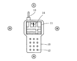
最近の携帯電話には、自己の現在地をGPSを利用して認識し、現在地周辺の地図の配信を受けた上で、これをディスプレイ画面上に表示する機能が備わりつつある。また、二次元磁気センサを内蔵することによって、地磁気の方向を検出し、地図表示とともに、方位表示を行う機能をもった携帯電話も開発されている。たとえば、図26に示す携帯電話10は、液晶からなるディスプレイ画面11、操作ボタン12、アンテナ13を備えており、ディスプレイ画面11には、現在地周辺の地図が表示されている。また、内蔵した二次元磁気センサにより地磁気の方向を検出し、ディスプレイ画面11上に、北を示す指標14を表示する機能を有している。図示の例は、携帯電話10を水平に寝かして保持した状態を示しており、ユーザは、ディスプレイ画面11上に表示された北を示す指標14により、アンテナ13の示す方向が北であることを認識することができ、その結果、東西南北の方位が図示の方向であることを認識することができる。
【0072】
図27は、内蔵された二次元磁気センサの検出値に基いて、北を示す指標14を表示する原理を示す平面図である。いま、地磁気の磁力線Hが図の一点鎖線で示す方向を向いていたとする。ここで、携帯電話10を図のように水平に寝かした状態(ディスプレイ画面11が水平面を維持する状態)にすると、内蔵された二次元磁気センサによって、この地磁気の方向を認識することができる。すなわち、ディスプレイ画面11の横方向をX軸、縦方向(アンテナ13の伸びる方向)をY軸として、内蔵の二次元磁気センサが、互いに直交するX軸およびY軸方向の磁気成分を検出する機能をもっていたとすれば、この二次元磁気センサが検出した地磁気のX軸方向成分H(x)およびY軸方向成分H(y)は、図示のとおり、磁力線Hの各軸方向成分を示すものになる。ここで、携帯電話10に定義したY軸方向(アンテナ13の伸びる方向)と磁力線Hとのなす角をφとすれば、
φ=arc tan (H(x)/H(y))
なる演算により、地磁気の方向のY軸に対する変位角φを求めることができ、この変位角φに基いて、ディスプレイ画面11上に方位表示を行うことができる。図示の例では、北を示す指標14がY軸方向に対して角度φだけ変位した向きに表示されており、携帯電話が電子コンパスとしての機能を果たしていることになる。
【0073】
このような方位表示は、本来、携帯電話10を水平状態にした場合にのみ意味をもつものである。すなわち、図28の側面図に示すように、地面Eに対してディスプレイ画面11が平行になるような状態にすれば、ディスプレイ画面11の表示面であるXY平面は、地面Eと平行になる。したがって、内蔵の磁気センサ15の検出値に基いて、図27に示すように北を示す指標14を表示すれば、この指標14の向きと磁力線Hの向きとが一致することになる。ところが、図29の側面図に示すように、携帯電話10が水平面に対して所定角ξだけ傾斜していると、ディスプレイ画面11の表示面(XY平面)も地面E(水平面)に対して角ξだけ傾斜することになるので、北を示す指標14も、地面Eに対して角ξだけ斜め上方を向くことになり、本来の磁力線Hの向き(北の方角)からずれてしまう。傾斜角ξが比較的小さい場合には、図29のように傾斜した状態においてディスプレイ画面11上に表示された方位表示を、図28のように水平に寝かした場合の状態を示す仮想的な方位表示として認識すれば、それなりの意味のある表示として把握することはできる。しかしながら、傾斜角ξが大きくなると、ディスプレイ画面11上の方位表示と、実際の地理的な方角との対応関係は著しく失われることになる。
【0074】
一般ユーザは、携帯電話の本来の機能である通信機能を利用する際に、携帯電話10をある程度立てた状態にして、操作ボタン12を操作するのが習慣となっている。このため、電子コンパスとしての機能を利用する際にも、携帯電話10をある程度立てた状態にして、ディスプレイ画面11を確認することも少なくない。ところが、上述したように、ディスプレイ画面11の傾斜角ξが大きくなればなるほど、ディスプレイ画面11上の方位表示のもつ意味は失われることになる。また、携帯電話10を立てた状態にすればするほど、磁気センサ15によって検出可能な磁力線Hの成分(図27に示すX軸方向成分およびY軸方向成分)は小さくなり、地磁気の検出感度は低下する。特に、図30に示すように、傾斜角ξ=90°となるように携帯電話10を完全に立てた状態にすると、ディスプレイ画面11の表示面(XY平面)は地面Eに対して直交することになるため、磁力線Hを検出することができなくなる。
【0075】
なお、ここでは便宜上、地磁気を示す磁力線Hが、地面Eに対して平行な方向を向いているという前提で説明を行ったが、実際には、地磁気を示す磁力線Hは、地面Eに対して完全には平行になっていない。しかも、磁力線Hの地面Eに対する角度は、地球上の個々の場所ごとにそれぞれ異なっている。このため、上述の理論は、厳密には、地球上の個々の地点で実際に生じる現象そのものではなく、若干の誤差を含んだ理論ということになるが、ここに示す実施形態の説明では、地磁気を示す磁力線Hは、便宜的に、地面Eに対して平行なものとして取り扱うことにする。
【0076】
このように、従来の携帯電話、GPS装置、PDA装置など、方位表示を行う機能をもった携帯型情報処理装置は、二次元磁気センサを利用して方位表示を行っていたため、ディスプレイ画面11の傾斜具合により、最適な方位表示が行われていないにもかかわらず、それをユーザに報知することはできなかった。ところが、本発明に係る三次元磁気センサをこのような携帯電話などに内蔵させるようにすると、このような問題を解決することができるようになる。以下、本発明に係る三次元磁気センサを内蔵した方位表示を行う機能をもった携帯電話の実施例を述べる。
【0077】
ここで述べる実施例に係る携帯電話の外観は、上述した従来の携帯電話10の外観と全く同じであり、図26に示すように、ディスプレイ画面11、操作ボタン12、アンテナ13が設けられている。また、図27に示すように、北を示す指標14を表示する機能を有している。ただ、携帯電話10に内蔵されている磁気センサ15は、従来のようなXY二次元座標系の磁気センサではなく、たとえば、図3に示すようなIJK座標系の磁気センサとなっている。もっとも、このIJK座標系の磁気センサ15による検出値は、XYZ三次元直交座標系の検出値に変換されることになる。
【0078】
図31は、この実施形態に係る携帯電話における、方位表示に直接関連する構成要素を示すブロック図である。もちろん、この携帯電話には、本来の通信機能を果たす構成要素が備わっているが、図31では、方位表示に直接関連しない構成要素については図示を省略してある。IJK座標系磁気センサ15は、既に述べてきたように、それぞれI軸、J軸、K軸を検出軸とする3つの磁気検出素子を有しており、各軸方向の地磁気の検出値H(i),H(j),H(k)を出力する機能を有する。座標系変換部16は、このようなIJK座標系の検出値を、XYZ三次元直交座標系の検出値H(x),H(y),H(z)に変換する機能を有している。このとき、XYZ三次元直交座標系は、XY平面がディスプレイ画面11と平行になり、Z軸がディスプレイ画面11に直交するように、携帯電話10に固定された座標系として定義されることになる。もちろん、このXYZ三次元直交座標系は、図28,図29,図30の側面図に示されているとおり、携帯電話10の傾斜とともに傾斜する座標系になる。
【0079】
こうして得られたXYZ三次元直交座標系の検出値のうち、検出値H(x),H(y),H(z)は、傾斜度認識部17へ与えられる。また、検出値H(x),H(y)は、方位表示部18にも与えられる(後述するように、方位表示部18は、Z軸方向成分H(z)を必要としない)。
【0080】
方位表示部18は、与えられた検出値H(x),H(y)に基いて、ディスプレイ画面11上に方位表示を行う機能を有する。この機能は、上述した従来の二次元磁気センサを内蔵した携帯電話における方位表示機能と同等である。すなわち、検出されたX軸方向成分H(x)およびY軸方向成分H(y)に基いて、
φ=arc tan (H(x)/H(y))
なる演算により、地磁気の方向のY軸に対する変位角φを求め、図27に示すように、変位角φに基いてディスプレイ画面11上に方位表示を行う。
【0081】
一方、傾斜度認識部17は、3つの検出値H(x),H(y),H(z)に基いて、ディスプレイ画面11の水平面に対する傾斜度を認識する構成要素である。傾斜度認識部17による傾斜度認識を行うようにした目的は、ディスプレイ画面11上に、方位表示部18による方位表示が行われている際に、傾斜度認識部17によって認識された傾斜度の程度をユーザに報知する機能を設け、方位表示が正しいものであるか否かの判断材料をユーザに提供できるようにする点にある。ここに示す実施例の場合、方位表示部18に、傾斜度認識部17による認識結果に基いて、方位表示の形態を異ならせる機能をもたせ、傾斜度の程度をユーザに報知するようにしている。具体的には、たとえば、傾斜度が所定のしきい値を越えていた場合に、ユーザに対する警告表示を行うようにしておけばよい。警告表示は、ディスプレイ画面11上に所定の方法で行うようにする。もっとも、ユーザに対する警告は、必ずしも視覚的認識が可能な表示という形式で行う必要はなく、音などによる警告を行ってもよい。
【0082】
たとえば、方位表示部18が、図27に示すように、北を示す指標14をディスプレイ画面11上に表示する処理を実行しているときに、傾斜度が所定のしきい値を越えた場合、この方位表示の指標14を点滅させることにより、ユーザに対して警告を行うようにしておけば、ユーザは、携帯電話10全体を寝かせるようにしないと、正しい方位表示が行われない可能性があることを認識することができる。あるいは、傾斜度が所定のしきい値を越えた場合に、ユーザに対する何らかのメッセージを表示するようにしてもよい。たとえば、図27のディスプレイ画面11上に、北を示す指標14とともに、「正確な方位表示を行うために、装置を寝かせてください!」といったメッセージを表示するようにすれば、ユーザに対して適切な警告を行うことが可能になる。もちろん、上記メッセージを音声で発し、警告を行うようにしてもよい。
【0083】
傾斜度に関するしきい値は、たとえば、図29に示すような傾斜角ξを定義しておき、ξ=45°のように、絶対的な角度値として設定することも可能であるが、三次元磁気センサ15の出力に基いて相対的なしきい値を設定してもよい。具体的には、傾斜度認識部17に、検出された地磁気のX軸方向成分H(x)およびY軸方向成分H(y)を合成した大きさと、Z軸方向成分H(z)の大きさと、を比較することにより傾斜度の認識を行う機能を設けておけばよい。ここに示す実施例では、図31の傾斜度認識部17のブロック内に示されているとおり、次の2とおりの比較方法を用意している。第1の比較方法は、(H(x)2+H(y)2)の平方根と、H(z)の絶対値と、を比較する方法である。第2の比較方法は、H(x)の絶対値とH(y)の絶対値との和と、H(z)の絶対値と、を比較する方法である。いずれの場合も、後者が前者よりも大きい場合には、傾斜度がしきい値を越えたものと判断し、傾斜度認識部17から方位表示部18に対して、その旨を示す報知信号が出力されるようにする。実用上は、いずれか一方の比較方法を採るか、あるいは、2つの比較方法を併用し、いずれか一方の比較方法においてしきい値を越えた場合には報知信号を出力するようにすればよい。方位表示部18は、このような報知信号を受け取ったときに、上述した種々の方法により、ディスプレイ画面11上に何らかの警告表示を行う。
【0084】
以上述べた方法は、傾斜度認識部17によって、傾斜度がしきい値を越えたか否かを認識し、越えた場合には、方位表示部18によって所定の警告表示を行う、という手法であり、ユーザには、傾斜度がしきい値を越えたか否かという二値情報のみが報知されることになる。これに対して、認識された傾斜度に関するより詳しい情報をユーザに報知することも可能である。たとえば、傾斜度が所定のしきい値を越えた場合には、上述したように、方位表示を点滅させるようにし、更に、傾斜度が大きくなるほど、点滅速度を速めるような設定を行うことも可能である。あるいは、方位表示の指標の全長を変えることにより、ユーザに傾斜度の程度を報知するようにしてもよい。具体的には、方位表示の指標の全長を、傾斜度が大きくなるほど短く表示するようにしておけば、ユーザは、指標の長さによって傾斜度を認識することができ、指標が短くなっていた場合には、携帯電話10を水平になるように傾けることにより、指標を伸ばす操作を行うことができるようになる。
【0085】
なお、傾斜度認識部17によって認識された傾斜度の程度をユーザに報知する方法としては、必ずしも視覚的な報知方法を採る必要はない。ここに示す実施形態では、図31のブロック図に示すように、振動機能駆動部19を更に設け、傾斜度が所定のしきい値を越えていた場合に、携帯電話10全体を振動させることにより、振動により傾斜度の程度をユーザに報知できるようにしてある。すなわち、傾斜度認識部17により、傾斜度がしきい値を越えたものと判断された場合、その旨を示す報知信号が、方位表示部18と振動機能駆動部19との双方に与えられる。この報知信号を受け取った方位表示部18は、既に述べたように、ディスプレイ画面11上に何らかの警告表示を行うことにより、ユーザに視覚的な報知を行う。一方、この報知信号を受け取った振動機能駆動部19は、携帯電話10を振動させることにより、ユーザに触覚的な報知を行うことになる。一般的な携帯電話には、ユーザに着信を知らせるための振動機能が備わっているものが多い。振動機能駆動部19は、このような着信を知らせるための既存の振動機能を利用して構成するようにすればよい。
【0086】
【発明の効果】
以上のとおり、本発明に係る三次元磁気センサによれば、支持基板上に形成した斜面に磁気検出素子を配置するようにしたため、小型化および量産化に適した構造を得ることができるようになる。
【図面の簡単な説明】
【図1】従来の一般的な三次元磁気センサにおける3つの磁気検出素子の配置例を示す斜視図である。
【図2】本発明に係る三次元磁気センサにおける3つの磁気検出素子の配置例を示す斜視図である。
【図3】本発明の第1の実施例に係る三次元磁気センサの基本構造を示す斜視図である。
【図4】図3に示す三次元磁気センサの上面図である。
【図5】図4に示す三次元磁気センサを切断線5−5に沿って切断した断面図である。
【図6】図5に示す三次元磁気センサにおいて、3つの磁気検出素子M11,M12,M13の各検出軸I,J,Kと、三次元直交座標系の各座標軸X,Y,Zとの幾何学的な位置関係を示す図である。
【図7】本発明に係る三次元磁気センサにおいて直交座標系の検出値を得るために必要な信号処理回路を示すブロック図である。
【図8】本発明の第2の実施例に係る三次元磁気センサの基本構造を示す上面図である。
【図9】図8に示す三次元磁気センサを切断線9−9に沿って切断した断面図である。
【図10】図9に示す三次元磁気センサにおいて、3つの磁気検出素子M11,M12,M13の各検出軸I,J,Kと、三次元直交座標系の各座標軸X,Y,Zとの幾何学的な位置関係を示す図である。
【図11】本発明の第3の実施例に係る三次元磁気センサの基本構造を示す上面図である。
【図12】図11に示す三次元磁気センサを切断線12−12に沿って切断した断面図である。
【図13】図12に示す三次元磁気センサにおいて、3つの磁気検出素子M11,M12,M13の各検出軸I,J,Kと、三次元直交座標系の各座標軸X,Y,Zとの幾何学的な位置関係を示す図である。
【図14】本発明に係る三次元磁気センサの磁気検出素子として利用可能なホール素子の第1の利用形態を示す図である。
【図15】本発明に係る三次元磁気センサの磁気検出素子として利用可能なホール素子の第2の利用形態を示す図である。
【図16】本発明に係る三次元磁気センサの磁気検出素子として利用可能な異方性磁気抵抗素子の利用形態を示す図である。
【図17】異方性磁気抵抗素子によって、磁界の向きまでも検出する手法を示す平面図である。
【図18】図17に示す手法に基いて、異方性磁気抵抗素子にバイアス磁界を加える方法を示す平面図である。
【図19】図18に示す4つの異方性磁気抵抗素子によりブリッジ回路を構成する配線を示す配線図である。
【図20】図19に示す配線によって構成されたブリッジ回路を示す回路図である。
【図21】図3に示す三次元磁気センサを製造する第1段階として、シリコン基板上にレジスト層を形成した状態を示す側断面図である。
【図22】図3に示す三次元磁気センサを製造する第2段階として、異方性エッチングにより、溝Gを形成した状態を示す側断面図である。
【図23】図3に示す三次元磁気センサを製造する第3段階として、溝Gを含むシリコン基板の上面に酸化膜を形成した状態を示す側断面図である。
【図24】図3に示す三次元磁気センサを製造する第4段階として、酸化膜上に磁気検出素子の層を形成した状態を示す側断面図である。
【図25】図3に示す三次元磁気センサを製造する第5段階として、磁気抵抗素子に対する配線層を形成した状態を示す側断面図である。
【図26】地図および方位表示の機能をもった一般的な携帯電話の外観を示す平面図である。
【図27】一般的な携帯電話において、北を示す指標を表示する原理を示す平面図である。
【図28】一般的な携帯電話を水平に寝かした状態を示す側面図である。
【図29】一般的な携帯電話を傾斜角ξだけ傾斜させた状態を示す側面図である。
【図30】一般的な携帯電話を垂直に立てた状態を示す側面図である。
【図31】本発明に係る三次元磁気センサを携帯電話に内蔵させ、方位表示を行う場合の関連構成要素を示すブロック図である。
【符号の説明】
10…装置本体
11…ディスプレイ画面
12…操作ボタン
13…アンテナ
14…北を示す指標(方位表示)
15…磁気センサ
16…座標系変換部
17…傾斜度認識部
18…方位表示部
19…振動機能駆動部
50…基板
51…基板の上面
52…基板の側面
60…基板
61…基板の上面
62…基板の斜面
80…座標系変換部
100…支持基板
110…溝Gの第1の側面
120…溝Gの第2の側面
130…溝Gの第3の側面
140…溝Gの第4の側面
150…溝Gの底面
160…支持基板の上面
200…シリコン基板
210…レジスト層
220…シリコン酸化膜
AMR1〜AMR4…磁気抵抗素子
a,b…磁気抵抗素子の両端
C1,C2…コイル
E…地面
F1,F2…バイアス磁界の磁力線
G…溝
H…検出対象磁気
H0…バイアス磁界
H(x)…磁気のX軸方向成分
H(y)…磁気のY軸方向成分
H(z)…磁気のZ軸方向成分
H(i)…磁気のI軸方向成分
H(j)…磁気のJ軸方向成分
H(k)…磁気のK軸方向成分
I,J,K,V…非直交座標系の座標軸
i,i1,i2…電流
M1,M2…磁気検出素子
M11〜M13…磁気検出素子
M12〜M23…磁気検出素子
M31〜M33…磁気検出素子
Ma…異方性磁気抵抗素子
Mh…ホール素子
Mv,Mx,My,Mz…磁気検出素子
O,Q…座標系の原点
R,R0,ΔR…抵抗値
T1〜T4…端子
V…検出電圧
W1,W2…配線層
X,Y,Z…直交座標系の座標軸
θ…支持基板の主面に対する斜面の傾斜角
φ…水平面上での磁力線の変位角
ξ…水平面に対する傾斜角[0001]
BACKGROUND OF THE INVENTION
The present invention relates to a three-dimensional magnetic sensor and a manufacturing method thereof, and more particularly to a three-dimensional magnetic sensor suitable for mass production using a semiconductor manufacturing technique and a micromachining technique and a manufacturing method thereof.
[0002]
[Prior art]
Magnetism is a vector quantity having a magnitude and direction in a three-dimensional space, and magnetism at an arbitrary point should be detected as a three-dimensional vector. However, it is not always necessary to detect magnetism as a three-dimensional vector quantity, and it is sufficient if a necessary direction component can be detected according to the application. For example, in an application for detecting a magnetic material, if the magnitude of magnetism can be detected, it is not necessary to specify the exact direction. Moreover, in the application which detects the rotational speed of a motor, it is enough if the magnetic component of a specific direction can be detected. For this reason, most of the magnetic sensors currently used are one-dimensional magnetic sensors having a function of detecting only a magnetic component in a predetermined detection axis direction.
[0003]
Since the action of magnetism is closely related to various electrical phenomena, many magnetic sensors use a magnetic detection element that can detect magnetism as an electrical quantity. For example, a magnetic detection element that detects magnetism as an electromotive force using the Hall effect and a magnetic detection element that detects magnetism as a change in resistance value using the magnetoresistance effect are generally used.
[0004]
Of course, there are cases where two-dimensional magnetic sensors and three-dimensional magnetic sensors are used depending on the application, but many of these multi-dimensional magnetic sensors are obtained by changing a plurality of one-dimensional magnetic sensors by changing the detection axis directions. It has an arranged configuration. For example, if two sets of one-dimensional magnetic sensors are arranged so that their detection axes are orthogonal to each other, a two-dimensional magnetic sensor can be realized, and three sets of one-dimensional magnetic sensors can be set so that their detection axes are orthogonal to each other. If it arrange | positions to, a three-dimensional magnetic sensor is realizable.
[0005]
[Problems to be solved by the invention]
As described above, since the conventional general three-dimensional magnetic sensor is a combination of three sets of one-dimensional magnetic sensors, it is difficult to reduce the size due to its physical structure. It is not suitable for mass production. However, for the past several years, the demand for small-sized three-dimensional magnetic sensors suitable for mass production has been increasing. In particular, in a portable information processing device incorporating an electronic compass and a GPS function, a function of recognizing the direction by detecting geomagnetism with high accuracy is indispensable, and development of a small three-dimensional magnetic sensor is desired. In addition, a head-mounted display used for providing a virtual reality environment also requires a small three-dimensional magnetic sensor for detecting geomagnetism. Recently, general-purpose small portable devices such as mobile phones and PDA devices have been put into practical use with electronic compass and GPS functions, and miniaturization and mass production of three-dimensional magnetic sensors have become an urgent task. Yes.
[0006]
Accordingly, an object of the present invention is to provide a three-dimensional magnetic sensor suitable for miniaturization and mass production.
[0007]
[Means for Solving the Problems]
(1) A first aspect of the present invention is a three-dimensional magnetic sensor for detecting each coordinate axis direction component of magnetism in an XYZ three-dimensional orthogonal coordinate system.
A support substrate having a slope inclined with respect to the main surface;
A first magnetic detection element, a second magnetic detection element, a third magnetic detection element formed on a predetermined surface of the support substrate;
A coordinate system conversion unit having a function of performing a conversion operation from the first coordinate system to the second coordinate system for a three-dimensional vector;
Provided,
At least one of the three magnetic detection elements is formed on a slope,
When I-axis, J-axis, and K-axis satisfying all the following three conditions are defined,
(Condition 1) Each axis faces either “a direction parallel to the upper surface or slope of the support substrate” or “a direction perpendicular to the upper surface or slope of the support substrate”,
(Condition 2) “All three axes of I axis, J axis and K axis are not included in the same plane”.
(Condition 3) The I-axis, J-axis, and K-axis are in different directions.
The first magnetic detection element detects the I-axis direction component H (i) of the detection target magnetism, the second magnetic detection element detects the J-axis direction component H (j) of the detection target magnetism, and the third magnetism. The detection element detects the K-axis direction component H (k) of the detection target magnetism,
The coordinate system conversion unit converts the three-dimensional magnetic vector of the IJK coordinate system indicated by the three-axis direction components H (i), H (j), and H (k) into the X-axis direction components H (x), An operation for converting the three-dimensional vector of the XYZ three-dimensional orthogonal coordinate system indicated by the three-axis direction component of the Y-axis direction component H (y) and the Z-axis direction component H (z) is performed.
[0008]
(2) According to a second aspect of the present invention, in the three-dimensional magnetic sensor according to the first aspect described above,
A groove having an inclined side surface is formed on the support substrate, and at least one magnetic detection element is formed on the side surface of the groove.
[0009]
(3) A third aspect of the present invention is the three-dimensional magnetic sensor according to the second aspect described above,
A square pyramid-shaped or truncated quadrangular pyramid-shaped groove is formed on the support substrate.
[0010]
(4) A fourth aspect of the present invention is the three-dimensional magnetic sensor according to the third aspect described above,
A support substrate is constituted by a silicon substrate having a (100) plane as a main surface, and each side surface of the groove is a (111) plane.
[0011]
(5) A fifth aspect of the present invention is the three-dimensional magnetic sensor according to the fourth aspect described above,
A silicon oxide film or nitride film is formed on at least a portion of the surface of the support substrate where the magnetic detection element is disposed.
[0012]
(6) A sixth aspect of the present invention is the three-dimensional magnetic sensor according to the fifth aspect described above,
A wiring layer for the magnetic sensing element is formed on the silicon oxide film or nitride film.
[0013]
(7) A seventh aspect of the present invention is the three-dimensional magnetic sensor according to the third to sixth aspects described above,
Each side surface of the quadrangular pyramid or truncated quadrangular pyramid forming the groove is defined as a first side surface, a second side surface, a third side surface, and a fourth side surface, and the first side surface and the third side surface are defined as When the definition is made such that the second side surface and the fourth side surface face each other, the first magnetic detection element and the second magnetic detection element are formed on the first side surface, A magnetic sensing element is formed on the third side;
When a cross section of a quadrangular pyramid or truncated quadrangular pyramid that forms a groove is defined by a plane that passes through the apex and is parallel to the upper side of the second side surface and the upper side of the fourth side surface is defined, The direction is the I axis that is the detection axis of the first magnetic detection element, the direction along the first side surface in this cross section is the J axis that is the detection axis of the second magnetic detection element, and the third axis in this cross section is the third axis. The direction along the side surface is the K axis that is the detection axis of the third magnetic detection element.
[0014]
(8) An eighth aspect of the present invention is the three-dimensional magnetic sensor according to the seventh aspect described above,
The X-axis in the direction of the upper side of the first side surface of the groove, the Y-axis in the direction of the upper side of the second side surface of the groove, the Z-axis in the direction perpendicular to the main surface of the substrate, the main surface of the substrate and the side surfaces of the groove When the angle formed by θ is θ, the coordinate system conversion unit
H (x) = H (i)
H (y) = (H (j) −H (k)) / 2 cos θ
H (z) = (H (j) + H (k)) / 2 sinθ
The three-dimensional magnetic vector of the IJK coordinate system is converted into the three-dimensional magnetic vector of the XYZ three-dimensional orthogonal coordinate system by executing the following calculation.
[0015]
(9) A ninth aspect of the present invention is the three-dimensional magnetic sensor according to the third to sixth aspects described above,
Each side surface of the quadrangular pyramid or truncated quadrangular pyramid forming the groove is defined as a first side surface, a second side surface, a third side surface, and a fourth side surface, and the first side surface and the third side surface are defined as When the definition is made such that the second side surface and the fourth side surface face each other, the second magnetic detection element is formed on the first side surface, and the first magnetic detection element and the third magnetic detection element The magnetic detection element is formed on the substrate main surface around the groove or the bottom surface of the groove,
When a cross section of a quadrangular pyramid or truncated quadrangular pyramid that forms a groove is defined by a plane that passes through the apex and is parallel to the upper side of the second side surface and the upper side of the fourth side surface is defined, The direction is the I axis that is the detection axis of the first magnetic detection element, the direction along the first side surface in this cross section is the J axis that is the detection axis of the second magnetic detection element, and the substrate main surface in this cross section The direction along the axis is the K axis which is the detection axis of the third magnetic detection element.
[0016]
(10) According to a tenth aspect of the present invention, in the three-dimensional magnetic sensor according to the ninth aspect described above,
The X-axis in the direction of the upper side of the first side surface of the groove, the Y-axis in the direction of the upper side of the second side surface of the groove, the Z-axis in the direction perpendicular to the main surface of the substrate, the main surface of the substrate and the side surfaces of the groove When the angle formed by θ is θ, the coordinate system conversion unit
H (x) = H (i)
H (y) = H (k)
H (z) = (H (j) −H (k) cos θ) / sin θ
The three-dimensional magnetic vector of the IJK coordinate system is converted into the three-dimensional magnetic vector of the XYZ three-dimensional orthogonal coordinate system by executing the following calculation.
[0017]
(11) An eleventh aspect of the present invention is the three-dimensional magnetic sensor according to the third to sixth aspects described above.
Each side surface of the quadrangular pyramid or truncated quadrangular pyramid forming the groove is defined as a first side surface, a second side surface, a third side surface, and a fourth side surface, and the first side surface and the third side surface are defined as When the definition is made such that the second side surface and the fourth side surface face each other, the first magnetic detection element is formed on the first side surface, and the second magnetic detection element is Forming a third magnetic detection element on the third side surface;
The direction perpendicular to the first side surface is the I axis that is the detection axis of the first magnetic detection element, the direction perpendicular to the second side surface is the J axis that is the detection axis of the second magnetic detection element, and the third The direction perpendicular to the side surface is the K axis which is the detection axis of the third magnetic detection element.
[0018]
(12) A twelfth aspect of the present invention is the three-dimensional magnetic sensor according to the eleventh aspect described above,
The X-axis in the direction of the upper side of the first side surface of the groove, the Y-axis in the direction of the upper side of the second side surface of the groove, the Z-axis in the direction perpendicular to the main surface of the substrate, the main surface of the substrate and the side surfaces of the groove When the angle formed by θ is θ, the coordinate system conversion unit
H (x) = (H (i) −H (k)) / 2 sinθ
H (y) = (2 · H (j) − (H (i) + H (k))) / 2 sin θ
H (z) = (H (i) + H (k)) / 2 cos θ
The three-dimensional magnetic vector of the IJK coordinate system is converted into the three-dimensional magnetic vector of the XYZ three-dimensional orthogonal coordinate system by executing the following calculation.
[0019]
(13) A thirteenth aspect of the present invention is the three-dimensional magnetic sensor according to the first to twelfth aspects described above,
A Hall element is used as the magnetic detection element. For this Hall element, three directions orthogonal to each other are defined, and the electromotive force generated in the second direction when current flows in the first direction is measured. The magnetic component directed in the direction of 3 can be detected.
[0020]
(14) The fourteenth aspect of the present invention is the three-dimensional magnetic sensor according to the first to twelfth aspects described above,
A magnetoresistive element is used as the magnetic detection element, and a predetermined direction component of magnetism can be detected based on a change in the resistance value of the magnetoresistive element.
[0021]
(15) According to a fifteenth aspect of the present invention, in the three-dimensional magnetic sensor according to the fourteenth aspect described above,
An anisotropic magnetoresistive element is used as the magnetic sensing element, a predetermined voltage is applied in a direction orthogonal to the detection axis of the anisotropic magnetoresistive element, and the current value of the current flowing in the voltage application direction is changed. Thus, the magnetic detection axis direction component can be detected.
[0022]
(16) A sixteenth aspect of the present invention is the three-dimensional magnetic sensor according to the fifteenth aspect,
A magnetic field generator for applying a bias magnetic field in a predetermined direction along the detection axis of the anisotropic magnetoresistive element is provided so that the direction along with the magnitude of magnetism can be detected by increasing or decreasing the current value with respect to the reference value.
[0023]
(17) According to a seventeenth aspect of the present invention, in the three-dimensional magnetic sensor according to the sixteenth aspect described above,
A coil is disposed in the vicinity of the anisotropic magnetoresistive element, and a bias magnetic field is generated by supplying current to the coil.
[0024]
(18) According to an eighteenth aspect of the present invention, in the three-dimensional magnetic sensor according to the sixteenth or seventeenth aspect described above,
Four sets of anisotropic magnetoresistive elements are arranged so that the detection axis is common, and the first anisotropic magnetoresistive element and the second anisotropic magnetoresistive element are arranged along the detection axis. A bias magnetic field is applied in the direction of 1, and a bias magnetic field is applied in a second direction opposite to the first direction for the third anisotropic magnetoresistive element and the fourth anisotropic magnetoresistive element. The bridge circuit is configured by these four sets of anisotropic magnetoresistive elements, and the magnitude and direction of the magnetic component along the detection axis can be detected based on the bridge voltage of the bridge circuit. It is what I did.
[0025]
(19) According to a nineteenth aspect of the present invention, in the method for manufacturing a three-dimensional magnetic sensor according to the first to eighteenth aspects described above,
Providing a silicon substrate having a (100) plane as the substrate upper surface;
Forming a mask layer having a square-shaped opening in the central portion on the upper surface of the silicon substrate;
Performing anisotropic etching on the silicon substrate on which the mask layer is formed, forming a groove having a quadrangular pyramid shape or a truncated quadrangular pyramid shape and having a side surface constituted by a (111) plane in a central portion of the upper surface; When,
Removing the mask layer;
Forming an insulating layer on the upper surface of the substrate including the inside of the formed groove;
Forming a magnetic sensing element at a predetermined location on the upper surface of the insulating layer;
Forming a wiring layer for the formed magnetic sensing element;
Is to do.
[0026]
(20) According to a twentieth aspect of the present invention, in the method for manufacturing a three-dimensional magnetic sensor according to the nineteenth aspect described above,
The step of forming the magnetic detection element is performed by forming a material layer for forming the magnetic detection element on the silicon oxide layer and then performing a patterning process so as to leave only a predetermined region portion of the material layer. It is a thing.
[0027]
(21) According to a twenty-first aspect of the present invention, in the method for manufacturing a three-dimensional magnetic sensor according to the nineteenth or twentieth aspect described above,
In the step of forming the wiring layer, a conductive layer for forming the wiring layer is formed on the silicon oxide layer or the magnetic detection element, and then a patterning process is performed so as to leave only a predetermined region portion of the conductive layer. It is something that is done by.
[0028]
DETAILED DESCRIPTION OF THE INVENTION
Hereinafter, the present invention will be described based on the illustrated embodiments.
[0029]
<<< §1. Basic principle of the present invention >>
An object of the present invention is to provide a three-dimensional magnetic sensor suitable for miniaturization and mass production, as already described. Generally, semiconductor manufacturing techniques and micromachining techniques are known as manufacturing techniques suitable for miniaturization and mass production of electronic devices. In these techniques, a semiconductor substrate such as silicon is often used as a material. The technology for forming various devices on a semiconductor substrate has been cultivated as an LSI manufacturing process for many years. In particular, LSI elements manufactured through the semiconductor planar process are very suitable for miniaturization and mass production. It becomes a thing. The starting point where the present inventor arrived at the idea of the present invention is that a three-dimensional magnetic sensor can be manufactured by using a manufacturing technique suitable for miniaturization and mass production used in an LSI element manufacturing process or the like. Ingenuity.
[0030]
Now, as shown in FIG. 1, let us consider a configuration of a three-dimensional magnetic sensor using some substrate 50 (for example, a silicon substrate). Here, the origin O of the coordinate system is taken at the right front corner of the
[0031]
As shown in FIG. 1, magnetic detection elements Mx and My are arranged on the
[0032]
On the other hand, in order to realize a three-dimensional magnetic sensor, it is necessary to further provide a magnetic detection element Mz having a function of detecting a magnetic Z-axis direction component. However, it is practically difficult to form the magnetic detection element Mz on the
[0033]
Eventually, if a three-dimensional magnetic sensor capable of detecting each coordinate axis direction component in the XYZ three-dimensional orthogonal coordinate system using the
[0034]
The present invention is for solving such a technical problem, and the most important idea thereof is to prepare a support substrate having a slope inclined with respect to the main surface, and among three magnetic detection elements. At least one of them is arranged on this slope. For example, consider a
[0035]
Here, the detection axis of the first magnetic detection element Mx is the X axis and the detection axis of the second magnetic detection element My is the Y axis, but the detection axis of the third magnetic detection element Mv is not the Z axis. It should be noted that the V axis is along the
[0036]
The inclination angle θ of the
[0037]
In FIG. 2, the
[0038]
In short, the essence of the present invention is that the first magnetic detection element of the three magnetic detection elements provided on the support substrate detects the I-axis direction component H (i) of the detection target magnetism, and the second magnetic The detection element detects the J-axis direction component H (j) of the detection target magnetism, and the third magnetic detection element detects the K-axis direction component H (k) of the detection target magnetism. By forming at least one of them on the slope of the support substrate, it is configured so that “all three axes of the I axis, the J axis, and the K axis are not included in the same plane”, and the I axis , J-axis, and K-axis are directed in different directions (the direction reversed by 180 ° is the same direction). If the setting that “all three axes of I axis, J axis, and K axis are included in the same plane” is made, the magnetic component in the direction perpendicular to the same plane cannot be detected. Therefore, it becomes impossible to detect the three-dimensional vector amount. Therefore, “any two of the three axes of the I axis, the J axis, and the K axis may be included in the same plane, but the third axis is not included in the same plane. It is natural that the condition of “to do” is necessary. In order to satisfy such a condition using three magnetic detection elements of the same type, it is necessary to form at least one element on an inclined surface with respect to the main surface of the substrate.
[0039]
If the magnetic components H (i), H (j), and H (k) can be detected for the three detection axes that satisfy the above-described conditions, that is, the I axis, the J axis, and the K axis, respectively, Is a value representing a three-dimensional magnetic vector to be detected in the IJK coordinate system. Therefore, the three-dimensional magnetic vector of the IJK coordinate system represented by the three-axis direction components H (i), H (j), and H (k) is converted into the X-axis direction component H (x) and the Y-axis direction component that are orthogonal to each other. A coordinate system conversion unit having a function of performing an operation of converting into a three-dimensional vector of an XYZ three-dimensional orthogonal coordinate system indicated by the three-axis direction component of H (y) and Z-axis direction component H (z) is prepared. If the original magnetic vector is converted and output from the IJK coordinate system to the XYZ coordinate system, the detection value of the XYZ three-dimensional orthogonal coordinate system can be obtained in the same manner as a conventional general three-dimensional magnetic sensor. it can.
[0040]
<<< §2. Basic Example >>>
Here, the three-dimensional magnetic sensor according to the present invention will be described based on some basic embodiments. In each of the examples shown here, a silicon substrate is used as a support substrate, a truncated regular quadrangular pyramid-shaped groove is formed in the center portion of the upper surface, and a magnetic detection element is disposed on an inclined surface formed by the side surface of the groove. It is.
[0041]
FIG. 3 is a perspective view showing the basic structure of the three-dimensional magnetic sensor according to the first embodiment. A groove G having a square opening is formed in the center of the upper surface of the
[0042]
4 is a top view of the three-dimensional magnetic sensor shown in FIG. 3, and FIG. 5 is a cross-sectional view of the three-dimensional magnetic sensor shown in FIG. 4 cut along a cutting line 5-5. Here, as shown in FIG. 3, the origin O is taken at the right front corner of the bottom of the
[0043]
On the other hand, each of the three magnetic detection elements M11, M12, and M13 is an elongated layered element. Here, the detection axes of these elements are referred to as an I axis, a J axis, and a K axis, respectively. In this embodiment, each magnetic detection element has a detection axis that is orthogonal to the longitudinal direction and faces the layer direction. Specifically, a cross section shown in FIG. 5 (a cross section obtained by cutting a truncated square pyramid forming the groove G along a plane parallel to the upper side of the
[0044]
FIG. 6 is a diagram showing a geometric positional relationship between the detection axes I, J, and K of the three magnetic detection elements M11, M12, and M13 and the coordinate axes X, Y, and Z of the three-dimensional orthogonal coordinate system. is there. If the angle formed between the
[0045]
In the specific geometric configuration shown in the upper part of FIG. 6, the coordinate axis I is equivalent to the coordinate axis X, and the coordinate axes J and K are included on the YZ plane and are inclined by an angle ± θ with respect to the Y axis. Therefore, finally, the relationship shown in the lower part of FIG. 6 is uniquely determined by the geometric operation using the trigonometric function. That is,
H (x) = H (i)
H (y) = (H (j) −H (k)) / 2 cos θ
H (z) = (H (j) + H (k)) / 2 sinθ
It is possible to convert the three-dimensional magnetic vector H of the IJK coordinate system into the three-dimensional magnetic vector H of the XYZ three-dimensional orthogonal coordinate system by executing the following calculation.
[0046]
After all, if the three magnetic detection elements M11, M12, and M13 are arranged as shown on the
[0047]
As described above, in the three-dimensional magnetic sensor according to the present invention, it is necessary to perform a predetermined coordinate system conversion operation on the detection values from the three magnetic detection elements, and therefore, it is necessary to provide the coordinate
[0048]
FIG. 8 is a top view showing a basic structure of the three-dimensional magnetic sensor according to the second embodiment, and FIG. 9 is a cross-sectional view of the three-dimensional magnetic sensor shown in FIG. 8 cut along a cutting line 9-9. . The basic structure of the
[0049]
FIG. 10 is a diagram showing a geometric positional relationship between the detection axes I, J, K of the three magnetic detection elements M21, M22, M23 and the coordinate axes X, Y, Z of the three-dimensional orthogonal coordinate system. is there. If the angle between the
[0050]
10, the coordinate axis I is equivalent to the coordinate axis X, the coordinate axis K is equivalent to the coordinate axis Y, the coordinate axis J is included on the YZ plane, and is relative to the Y axis. Therefore, the relationship as shown in the lower part of FIG. 10 is finally determined by geometric calculation using a trigonometric function. That is,
H (x) = H (i)
H (y) = H (k)
H (z) = (H (j) −H (k) cos θ) / sin θ
It is possible to convert the three-dimensional magnetic vector H of the IJK coordinate system into the three-dimensional magnetic vector H of the XYZ three-dimensional orthogonal coordinate system by executing the following calculation. Therefore, as shown in FIG. 7, the detection values H (x), H (y), and H (z) of the XYZ coordinate system can be obtained by performing the coordinate system conversion process by the coordinate
[0051]
FIG. 11 is a top view showing a basic structure of a three-dimensional magnetic sensor according to the third embodiment, and FIG. 12 is a cross-sectional view of the three-dimensional magnetic sensor shown in FIG. 11 cut along a cutting line 12-12. . The basic structure of the
[0052]
These three magnetic detection elements M31, M32, and M33 are the same as the conventional magnetic detection elements in that they are all elongated layered elements. However, the direction of the magnetic detection axis is significantly different from the magnetic detection elements described so far. That is, the detection surfaces of the three magnetic detection elements M31, M32, and M33 are all perpendicular to the layer surface. If the detection axes of these elements are referred to as the I axis, the J axis, and the K axis, respectively, the direction perpendicular to the
[0053]
FIG. 13 is a diagram showing a geometric positional relationship between the detection axes I, J, and K of the three magnetic detection elements M31, M32, and M33 and the coordinate axes X, Y, and Z of the three-dimensional orthogonal coordinate system. is there. If the angle formed between each of the side surfaces 110 to 140 constituting the groove G and the main surface (upper surface or lower surface) of the
H (x) = (H (i) −H (k)) / 2 sinθ
H (y) = (2 · H (j) − (H (i) + H (k))) / 2 sin θ
H (z) = (H (i) + H (k)) / 2 cos θ
It is possible to convert the three-dimensional magnetic vector H of the IJK coordinate system into the three-dimensional magnetic vector H of the XYZ three-dimensional orthogonal coordinate system by executing the following calculation. Therefore, also in the third embodiment, as shown in FIG. 7, by performing a coordinate system conversion process by the coordinate
[0054]
The basic structure of the three-dimensional magnetic sensor according to the present invention has been described with respect to the three embodiments. Of course, the present invention is not limited to the embodiments. For example, the groove G formed in the
[0055]
In short, in the present invention, at least one of the three magnetic detection elements is formed on the inclined surface of the support substrate, and if there is a remainder, it is formed on the main surface of the support substrate. It is configured to avoid the situation that “all three axes of the axis and the K axis are included in the same plane”, and the directions in which the I axis, the J axis, and the K axis are different from each other (the direction reversed by 180 ° is also set to the same direction). ), The goal can be achieved.
[0056]
<<< §3. Specific examples of magnetic detection elements >>
As described above, in the three-dimensional magnetic sensor according to the present invention, it is necessary to prepare three magnetic detection elements arranged so that the directions of the detection axes are different from each other. Here, each magnetic detection element may be an element having a function of detecting a magnetic component in a predetermined detection axis direction. Known magnetic sensing elements having such properties include Hall elements, anisotropic magnetoresistive elements (AMR elements: Anisotropic MagnetoResistance), giant magnetoresistive elements (GMR elements: Giant MagnetoResistance), and the like. These elements can be used as the magnetic detection elements in the various embodiments described in (1).
[0057]
For example, when a Hall element is used as the magnetic detection element, three directions orthogonal to each other are defined for the Hall element, and the electromotive force generated in the second direction when current flows in the first direction is measured. This makes it possible to detect the magnetic component facing the third direction. Specifically, for example, as shown in FIG. 14, consider a case where an elongated layered Hall element Mh is prepared and a current i flows in the longitudinal direction thereof. In this case, when the magnetic H acts in a direction parallel to the layer surface and perpendicular to the direction of the current i, a phenomenon (Hall effect) that generates an electromotive force V in a direction perpendicular to the layer surface (thickness direction) appears. If the electromotive force V is measured, it is possible to detect the direction and magnitude of the magnetic H that has acted. The Hall element having such a detection function can be used as a magnetic detection element in the first embodiment (FIG. 4) and the second embodiment (FIG. 8) described above.
[0058]
Alternatively, as shown in FIG. 15, if the electromotive force V generated in the width direction is measured in a state where the current i flows in the longitudinal direction of the elongated layered Hall element Mh, the direction of the magnetic H in the thickness direction and The size can be detected. The Hall element having such a detection function can be used as a magnetic detection element in the third embodiment (FIG. 11) described above.
[0059]
On the other hand, even if an anisotropic magnetoresistive element (hereinafter referred to as an AMR element) is used as the magnetic detection element, the same detection is possible. This AMR element has a property that the electric resistance changes when magnetism acts in a specific detection axis direction. Therefore, for example, as shown in FIG. 16, consider a case where an elongated layered AMR element Ma is prepared and a current i is passed in the longitudinal direction thereof. At this time, assuming that the detection axis is set in a direction parallel to the layer surface and perpendicular to the direction of the current i, when the magnetic H acts in the detection axis direction, the electric resistance R of the AMR element Ma Changes. Therefore, if a predetermined voltage is applied in the longitudinal direction of the AMR element Ma and the current i flowing at that time is measured, the magnetic H can be detected as the fluctuation of the current i. The AMR element having such a detection function can be used as a magnetic detection element in the first embodiment (FIG. 4) and the second embodiment (FIG. 8). Further, if an AMR element having a detection axis in a direction (thickness direction) perpendicular to the layer surface is used, it can be used as a magnetic detection element in the third embodiment (FIG. 11).
[0060]
However, this AMR element can detect the absolute value of the magnetism acting in the direction of a specific detection axis, but cannot detect the sign. That is, in FIG. 16, when the magnetic force directed from the near side to the far side of the AMR element Ma is applied, and conversely, when the magnetic force directed from the far side to the near side is applied, the absolute value of the applied magnetic force is the same. The change in resistance value R is the same. For this reason, it is not possible to perform magnetic detection in consideration of positive and negative signs (direction of magnetic force). This is a major drawback compared to the Hall element (in the case of the Hall element, the direction of the applied magnetic force can be recognized by the sign of the generated electromotive force V).
[0061]
In order to compensate for such drawbacks of the AMR element, a magnetic field generator for applying a bias magnetic field in a predetermined direction along the detection axis of the AMR element is provided, and the direction of the magnetic field is adjusted along with the magnitude of the magnetism by increasing or decreasing the current value with respect to the reference value. What is necessary is just to take the method of detecting. FIG. 17 is a plan view for explaining the principle of such a method. First, as shown in FIG. 17A, a constant voltage is applied in the longitudinal direction of the AMR element Ma so that the current i flows. At this time, a bias magnetic field H0 having a predetermined magnitude is applied from a direction along the detection axis (a direction perpendicular to the longitudinal direction in the drawing). In the figure, the bias magnetic field H0 is applied in the direction from the top to the bottom in the figure. However, the bias magnetic field H0 may be applied in the direction from the bottom to the top. When such a bias magnetic field H0 is applied, naturally the resistance value of the AMR element Ma changes, but here the resistance value R0 after the change caused by the bias magnetic field H0 is set as a reference value.
[0062]
Here, as shown in FIG. 17B, if the magnetic field H to be detected acts in the direction from the top to the bottom of the figure, the magnetic field acting on the AMR element Ma is the bias magnetic field H0 and the detection target. The sum of the magnetic field H and the resistance value of the AMR element Ma changes to R0 + ΔR. Here, ΔR is a change in resistance caused by the detection target magnetic field H. However, as shown in FIG. 17C, if the magnetic field H to be detected acts in the direction from the bottom to the top of the figure, the magnetic field acting on the AMR element Ma is the bias magnetic field H0 and the detection target magnetic field. The resistance value of the AMR element Ma changes to R0−ΔR. Eventually, the direction of the magnetic field H to be detected can be recognized depending on whether the actual resistance value has increased or decreased with respect to the reference resistance value R0. The magnitude of the magnetic field H can be recognized (actually, the increase / decrease of the current i with respect to the reference value is measured).
[0063]
In order to apply the bias magnetic field H0 to the AMR element Ma, a permanent magnet (for example, a rare earth permanent magnet) or a coil (for example, a thin film coil or an electromagnetic coil) may be disposed in the vicinity thereof. When a coil is disposed, a bias magnetic field H0 can be generated by supplying a current to the coil. FIG. 18 shows an example in which one magnetic detection element is constituted by an assembly of four sets of AMR elements so that detection with higher accuracy is possible. Here, each of AMR1 to AMR4 is an AMR element having a common detection axis in the direction D in the figure. As illustrated, a coil C1 is disposed on the left end a side of the
[0064]
Now, let us provide wiring as shown in the circuit diagram of FIG. 19 for these four sets of AMR elements. As illustrated, the right ends b of AMR1 and AMR3 are connected to a terminal T1, and the left ends a of AMR2 and AMR4 are connected to a terminal T4 (ground). The left end a of AMR1 and the right end b of AMR4 are connected to terminal T2, and the right end b of AMR2 and the left end a of AMR3 are connected to terminal T3. Further, as shown in the figure, a bias magnetic field F1 is applied to the
[0065]
In general, the AMR element has a property that the resistance value is changed not only by the influence of magnetism but also by the influence of temperature. As described above, when the bridge circuit is configured by four sets of AMR elements, the change in resistance value due to the influence of temperature can be canceled out, and magnetic detection with higher accuracy is possible. Since the three-dimensional magnetic sensor according to the present invention requires three magnetic detection elements, when each magnetic detection element is constituted by a bridge circuit composed of four sets of AMR elements, a total of 12 sets of AMR elements are provided. I need it.
[0066]
<<< §4. Manufacturing method of three-dimensional magnetic sensor according to the present invention >>
Subsequently, a specific manufacturing method of the three-dimensional magnetic sensor according to the present invention, particularly suitable for forming the main body of the sensor having a physical structure as shown in FIG. 3 using a semiconductor manufacturing process. Describe the method. In the
[0067]
Hereinafter, a specific manufacturing process will be described with reference to side sectional views. First, as shown in FIG. 21, a
[0068]
Subsequently, after removing the
[0069]
Finally, a wiring layer for the formed magnetic detection element is formed. FIG. 25 shows a state in which the wiring layers W1 and W2 are formed for the magnetic detection elements M1 and M2. Of course, in practice, many more complicated wiring layers are formed. In the step of forming the wiring layer, a metal conductive layer such as copper or aluminum for forming the wiring layer is formed into a thin film on the
[0070]
<<< §5. Application to devices with orientation display function >>>
As described above, the three-dimensional magnetic sensor according to the present invention is an apparatus suitable for downsizing and mass production, and can greatly reduce the manufacturing cost. For this reason, it is most suitable for use as a geomagnetic sensor built in a portable information processing apparatus having a direction display function such as a mobile phone or a GPS device. Here, a unique usage mode in which the three-dimensional magnetic sensor according to the present invention is built in a portable information processing apparatus having an orientation display function will be described.
[0071]
Recent mobile phones have a function of recognizing their current location using GPS, receiving a map around the current location, and displaying the map on a display screen. In addition, a mobile phone has been developed that has a function of detecting the direction of geomagnetism by incorporating a two-dimensional magnetic sensor and displaying a map as well as a direction. For example, the
[0072]
FIG. 27 is a plan view showing the principle of displaying the
φ = arc tan (H (x) / H (y))
By this calculation, the displacement angle φ with respect to the Y axis in the direction of geomagnetism can be obtained, and the azimuth can be displayed on the
[0073]
Such azimuth display is originally meaningful only when the
[0074]
It is customary for a general user to operate the
[0075]
Here, for the sake of convenience, the description has been made on the assumption that the magnetic lines of force H indicating the geomagnetism are oriented in a direction parallel to the ground E. However, in actuality, the magnetic lines of force H indicating the geomagnetism are relative to the ground E. It is not completely parallel. Moreover, the angle of the magnetic field lines H with respect to the ground E is different for each location on the earth. Therefore, strictly speaking, the above-mentioned theory is not a phenomenon that actually occurs at each point on the earth, but a theory that includes some errors, but in the explanation of the embodiment shown here, the geomagnetism For the sake of convenience, the magnetic lines of force H indicating the above are handled as being parallel to the ground E.
[0076]
As described above, since the portable information processing device having a function of performing orientation display, such as a conventional mobile phone, GPS device, or PDA device, performs orientation display using the two-dimensional magnetic sensor, Although the optimum orientation display is not performed due to the inclination, it has not been possible to notify the user of it. However, such a problem can be solved by incorporating the three-dimensional magnetic sensor according to the present invention in such a cellular phone. Hereinafter, an embodiment of a mobile phone having a function of performing azimuth display incorporating a three-dimensional magnetic sensor according to the present invention will be described.
[0077]
The appearance of the mobile phone according to the embodiment described here is exactly the same as the appearance of the conventional
[0078]
FIG. 31 is a block diagram showing components directly related to the orientation display in the mobile phone according to this embodiment. Of course, this mobile phone is provided with components that perform the original communication function, but in FIG. 31, the components that are not directly related to the orientation display are not shown. As described above, the IJK coordinate system
[0079]
Of the detected values of the XYZ three-dimensional orthogonal coordinate system thus obtained, the detected values H (x), H (y), and H (z) are given to the
[0080]
The
φ = arc tan (H (x) / H (y))
As a result, the displacement angle φ with respect to the Y-axis in the direction of geomagnetism is obtained, and the orientation is displayed on the
[0081]
On the other hand, the
[0082]
For example, when the
[0083]
As the threshold value related to the inclination, for example, an inclination angle ξ as shown in FIG. 29 is defined and can be set as an absolute angle value such as ξ = 45 °. A relative threshold value may be set based on the output of the
[0084]
The method described above is a method in which the
[0085]
As a method for notifying the user of the degree of inclination recognized by the
[0086]
【The invention's effect】
As described above, according to the three-dimensional magnetic sensor according to the present invention, since the magnetic detection element is arranged on the slope formed on the support substrate, a structure suitable for miniaturization and mass production can be obtained. Become.
[Brief description of the drawings]
FIG. 1 is a perspective view showing an arrangement example of three magnetic detection elements in a conventional general three-dimensional magnetic sensor.
FIG. 2 is a perspective view showing an arrangement example of three magnetic detection elements in the three-dimensional magnetic sensor according to the present invention.
FIG. 3 is a perspective view showing the basic structure of the three-dimensional magnetic sensor according to the first embodiment of the invention.
4 is a top view of the three-dimensional magnetic sensor shown in FIG.
5 is a cross-sectional view of the three-dimensional magnetic sensor shown in FIG. 4 cut along a cutting line 5-5.
6 is a diagram illustrating the three-dimensional magnetic sensor shown in FIG. 5 in which the detection axes I, J, and K of the three magnetic detection elements M11, M12, and M13 and the coordinate axes X, Y, and Z of the three-dimensional orthogonal coordinate system; It is a figure which shows geometric positional relationship.
FIG. 7 is a block diagram showing a signal processing circuit necessary for obtaining a detection value of an orthogonal coordinate system in the three-dimensional magnetic sensor according to the present invention.
FIG. 8 is a top view showing a basic structure of a three-dimensional magnetic sensor according to a second embodiment of the present invention.
9 is a cross-sectional view of the three-dimensional magnetic sensor shown in FIG. 8 cut along a cutting line 9-9.
10 is a diagram illustrating the three-dimensional magnetic sensor shown in FIG. 9 in which the detection axes I, J, and K of the three magnetic detection elements M11, M12, and M13 and the coordinate axes X, Y, and Z of the three-dimensional orthogonal coordinate system; It is a figure which shows geometric positional relationship.
FIG. 11 is a top view showing a basic structure of a three-dimensional magnetic sensor according to a third embodiment of the present invention.
12 is a cross-sectional view of the three-dimensional magnetic sensor shown in FIG. 11 cut along a cutting line 12-12.
13 is a diagram illustrating the three-dimensional magnetic sensor shown in FIG. 12 in which the detection axes I, J, and K of the three magnetic detection elements M11, M12, and M13 and the coordinate axes X, Y, and Z of the three-dimensional orthogonal coordinate system; It is a figure which shows geometric positional relationship.
FIG. 14 is a diagram showing a first usage pattern of the Hall element that can be used as the magnetic detection element of the three-dimensional magnetic sensor according to the present invention.
FIG. 15 is a diagram showing a second usage pattern of the Hall element that can be used as the magnetic detection element of the three-dimensional magnetic sensor according to the present invention.
FIG. 16 is a diagram showing an application form of an anisotropic magnetoresistive element that can be used as a magnetic detection element of a three-dimensional magnetic sensor according to the present invention.
FIG. 17 is a plan view showing a method for detecting even the direction of a magnetic field by an anisotropic magnetoresistive element.
18 is a plan view showing a method of applying a bias magnetic field to the anisotropic magnetoresistive element based on the method shown in FIG.
FIG. 19 is a wiring diagram showing wiring that constitutes a bridge circuit by the four anisotropic magnetoresistive elements shown in FIG. 18;
20 is a circuit diagram showing a bridge circuit configured by the wiring shown in FIG. 19;
FIG. 21 is a side sectional view showing a state in which a resist layer is formed on a silicon substrate as a first stage in manufacturing the three-dimensional magnetic sensor shown in FIG. 3;
22 is a side sectional view showing a state in which a groove G is formed by anisotropic etching as a second stage for manufacturing the three-dimensional magnetic sensor shown in FIG. 3;
23 is a side sectional view showing a state in which an oxide film is formed on the upper surface of a silicon substrate including a groove G as a third stage for manufacturing the three-dimensional magnetic sensor shown in FIG. 3;
24 is a side sectional view showing a state in which a layer of a magnetic detection element is formed on an oxide film as a fourth stage for manufacturing the three-dimensional magnetic sensor shown in FIG. 3;
25 is a side sectional view showing a state in which a wiring layer for the magnetoresistive element is formed as a fifth stage for manufacturing the three-dimensional magnetic sensor shown in FIG. 3;
FIG. 26 is a plan view showing an external appearance of a general mobile phone having a map and orientation display function.
FIG. 27 is a plan view showing the principle of displaying an index indicating north in a general mobile phone.
FIG. 28 is a side view showing a state in which a general mobile phone is laid down horizontally.
FIG. 29 is a side view showing a state in which a general mobile phone is inclined by an inclination angle ξ.
FIG. 30 is a side view showing a state in which a general mobile phone is set up vertically.
FIG. 31 is a block diagram showing related components when a three-dimensional magnetic sensor according to the present invention is built in a mobile phone to perform orientation display.
[Explanation of symbols]
10 ... Main body
11 ... Display screen
12. Operation buttons
13 ... Antenna
14 ... Indicator indicating north (direction display)
15 ... Magnetic sensor
16 ... coordinate system conversion unit
17 ... Inclination recognition unit
18 ... Direction display section
19 ... Vibration function drive unit
50 ... Board
51 ... Upper surface of substrate
52. Side surface of substrate
60 ... Board
61 ... Upper surface of substrate
62 ... Slope of substrate
80: Coordinate system conversion unit
100 ... support substrate
110... First side of groove G
120 ... Second side of groove G
130... Third side of groove G
140: Fourth side surface of groove G
150 ... bottom surface of groove G
160. Upper surface of support substrate
200: Silicon substrate
210 ... resist layer
220 ... Silicon oxide film
AMR1 to AMR4 ... magnetoresistive elements
a, b: Both ends of the magnetoresistive element
C1, C2 ... Coil
E ... ground
F1, F2 ... Magnetic field lines of bias magnetic field
G ... Groove
H ... Magnetic field to be detected
H0 ... Bias magnetic field
H (x): Magnetic X-axis direction component
H (y) ... Y-axis direction component of magnetism
H (z): Z-axis direction component of magnetism
H (i): Magnetic I-axis direction component
H (j): Magnetic J-axis direction component
H (k): K-axis component of magnetism
I, J, K, V ... Coordinate axes of non-orthogonal coordinate system
i, i1, i2 ... current
M1, M2 ... Magnetic detection element
M11 to M13 ... Magnetic detection element
M12 to M23 ... Magnetic detection element
M31 to M33 ... Magnetic detection element
Ma: anisotropic magnetoresistive element
Mh ... Hall element
Mv, Mx, My, Mz ... Magnetic detection element
O, Q ... Origin of coordinate system
R, R0, ΔR: Resistance value
T1 to T4 ... Terminal
V ... Detection voltage
W1, W2 ... Wiring layer
X, Y, Z ... Coordinate axes of Cartesian coordinate system
θ: Inclination angle of the slope with respect to the main surface of the support substrate
φ ... Displacement angle of magnetic field lines on the horizontal plane
ξ ... Inclination angle with respect to horizontal plane
Claims (21)
主面に対して傾斜した斜面を有する支持基板と、
前記支持基板の所定面上に形成された第1の磁気検出素子、第2の磁気検出素子、第3の磁気検出素子と、
三次元ベクトルについて、第1の座標系から第2の座標系への変換演算を行う機能をもった座標系変換部と、
を備え、
前記3つの磁気検出素子のうちの少なくとも1つは、前記斜面上に形成されており、
以下の3条件をすべて満足するI軸,J軸,K軸を定義したときに、
(条件1) 各軸は、それぞれ「前記支持基板の上面もしくは前記斜面に平行な方向」または「前記支持基板の上面もしくは前記斜面に対して垂直な方向」のいずれかを向いている、
(条件2) 「I軸,J軸,K軸の3軸すべてが同一平面上に含まれる」ことはない、
(条件3) I軸,J軸,K軸は互いに異なる方向を向いている、
前記第1の磁気検出素子は検出対象磁気のI軸方向成分H(i)を検出する機能を有し、前記第2の磁気検出素子は検出対象磁気のJ軸方向成分H(j)を検出する機能を有し、前記第3の磁気検出素子は検出対象磁気のK軸方向成分H(k)を検出する機能を有し、
前記座標系変換部は、前記H(i),H(j),H(k)の3軸方向成分で示されるIJK座標系の三次元磁気ベクトルを、互いに直交するX軸方向成分H(x),Y軸方向成分H(y),Z軸方向成分H(z)の3軸方向成分で示されるXYZ三次元直交座標系の三次元ベクトルに変換する演算を行うことを特徴とする三次元磁気センサ。A three-dimensional magnetic sensor for detecting each coordinate axis direction component of magnetism in an XYZ three-dimensional orthogonal coordinate system,
A support substrate having a slope inclined with respect to the main surface;
A first magnetic detection element, a second magnetic detection element, a third magnetic detection element formed on a predetermined surface of the support substrate;
A coordinate system conversion unit having a function of performing a conversion operation from the first coordinate system to the second coordinate system for a three-dimensional vector;
With
At least one of the three magnetic detection elements is formed on the slope,
When I-axis, J-axis, and K-axis satisfying all the following three conditions are defined,
(Condition 1) Each axis faces either one of “a direction parallel to the upper surface of the support substrate or the inclined surface” or “a direction perpendicular to the upper surface of the support substrate or the inclined surface”.
(Condition 2) “All three axes of I axis, J axis and K axis are not included in the same plane”.
(Condition 3) The I-axis, J-axis, and K-axis are in different directions.
The first magnetic detection element has a function of detecting an I-axis direction component H (i) of detection target magnetism, and the second magnetic detection element detects a J-axis direction component H (j) of detection target magnetism. The third magnetic detection element has a function of detecting a K-axis direction component H (k) of the detection target magnetism,
The coordinate system conversion unit converts the three-dimensional magnetic vector of the IJK coordinate system indicated by the three-axis direction components of H (i), H (j), and H (k) into an X-axis direction component H (x ), Y-axis direction component H (y), and Z-axis direction component H (z) are converted into a three-dimensional vector of an XYZ three-dimensional orthogonal coordinate system represented by the three-axis direction component. Magnetic sensor.
支持基板上に、傾斜した側面を有する溝が形成されており、この溝の側面に少なくとも1つの磁気検出素子が形成されていることを特徴とする三次元磁気センサ。The three-dimensional magnetic sensor according to claim 1,
A three-dimensional magnetic sensor, wherein a groove having an inclined side surface is formed on a support substrate, and at least one magnetic detection element is formed on the side surface of the groove.
支持基板上に、四角錐状もしくは裁頭四角錐状の溝が形成されていることを特徴とする三次元磁気センサ。The three-dimensional magnetic sensor according to claim 2,
A three-dimensional magnetic sensor, wherein a quadrangular pyramid-shaped or truncated quadrangular pyramid-shaped groove is formed on a support substrate.
(100)面を主面とするシリコン基板によって支持基板が構成されており、溝の各側面が(111)面によって構成されていることを特徴とする三次元磁気センサ。The three-dimensional magnetic sensor according to claim 3,
A three-dimensional magnetic sensor, wherein a support substrate is constituted by a silicon substrate having a (100) plane as a principal plane, and each side surface of the groove is constituted by a (111) plane.
支持基板の表面のうち、少なくとも磁気検出素子を配置する部分にシリコンの酸化膜もしくは窒化膜が形成されていることを特徴とする三次元磁気センサ。The three-dimensional magnetic sensor according to claim 4,
A three-dimensional magnetic sensor, wherein a silicon oxide film or a nitride film is formed at least on a portion of the surface of the support substrate where the magnetic detection element is disposed.
シリコンの酸化膜もしくは窒化膜上に、磁気検出素子に対する配線層が形成されていることを特徴とする三次元磁気センサ。The three-dimensional magnetic sensor according to claim 5,
A three-dimensional magnetic sensor, wherein a wiring layer for a magnetic detecting element is formed on a silicon oxide film or nitride film.
溝を形成する四角錐もしくは裁頭四角錐の各側面をそれぞれ第1の側面、第2の側面、第3の側面、第4の側面と定義し、前記第1の側面と前記第3の側面とが対向し、前記第2の側面と前記第4の側面とが対向するような定義を行ったときに、第1の磁気検出素子および第2の磁気検出素子が、前記第1の側面に形成されており、第3の磁気検出素子が、前記第3の側面に形成されており、
前記四角錐もしくは裁頭四角錐を、頂点を通り前記第2の側面の上辺および前記第4の側面の上辺に平行な面で切断した断面を定義したときに、前記断面に対して垂直な方向が前記第1の磁気検出素子の検出軸であるI軸となっており、前記断面における前記第1の側面に沿った方向が前記第2の磁気検出素子の検出軸であるJ軸となっており、前記断面における前記第3の側面に沿った方向が前記第3の磁気検出素子の検出軸であるK軸となっていることを特徴とする三次元磁気センサ。The three-dimensional magnetic sensor according to any one of claims 3 to 6,
Each side surface of the quadrangular pyramid or truncated quadrangular pyramid forming the groove is defined as a first side surface, a second side surface, a third side surface, and a fourth side surface, respectively, and the first side surface and the third side surface are defined. Are defined such that the second side surface and the fourth side surface are opposed to each other, the first magnetic detection element and the second magnetic detection element are disposed on the first side surface. A third magnetic detection element is formed on the third side surface;
A direction perpendicular to the cross section when defining a cross section obtained by cutting the quadrangular pyramid or truncated quadrangular pyramid at a plane passing through the apex and parallel to the upper side of the second side surface and the upper side of the fourth side surface Is the I axis that is the detection axis of the first magnetic detection element, and the direction along the first side surface in the cross section is the J axis that is the detection axis of the second magnetic detection element. A three-dimensional magnetic sensor, wherein a direction along the third side surface in the cross section is a K-axis that is a detection axis of the third magnetic detection element.
溝の第1の側面の上辺の方向にX軸、溝の第2の側面の上辺の方向にY軸、基板主面に対して垂直な方向にZ軸、基板主面と溝の各側面とのなす角をθとしたときに、座標系変換部が、
H(x)=H(i)
H(y)=(H(j)−H(k))/2 cosθ
H(z)=(H(j)+H(k))/2 sinθ
なる演算を実行することによって、IJK座標系の三次元磁気ベクトルを、XYZ三次元直交座標系の三次元磁気ベクトルに変換することを特徴とする三次元磁気センサ。The three-dimensional magnetic sensor according to claim 7,
The X-axis in the direction of the upper side of the first side surface of the groove, the Y-axis in the direction of the upper side of the second side surface of the groove, the Z-axis in the direction perpendicular to the main surface of the substrate, the main surface of the substrate and the side surfaces of the groove When the angle formed by θ is θ, the coordinate system conversion unit
H (x) = H (i)
H (y) = (H (j) −H (k)) / 2 cos θ
H (z) = (H (j) + H (k)) / 2 sinθ
A three-dimensional magnetic sensor that converts a three-dimensional magnetic vector of an IJK coordinate system into a three-dimensional magnetic vector of an XYZ three-dimensional orthogonal coordinate system by executing the following calculation.
溝を形成する四角錐もしくは裁頭四角錐の各側面をそれぞれ第1の側面、第2の側面、第3の側面、第4の側面と定義し、前記第1の側面と前記第3の側面とが対向し、前記第2の側面と前記第4の側面とが対向するような定義を行ったときに、第2の磁気検出素子が前記第1の側面に形成されており、第1の磁気検出素子および第3の磁気検出素子が、前記溝の周囲の基板主面もしくは溝の底面に形成されており、
前記四角錐もしくは裁頭四角錐を、頂点を通り前記第2の側面の上辺および前記第4の側面の上辺に平行な面で切断した断面を定義したときに、前記断面に対して垂直な方向が前記第1の磁気検出素子の検出軸であるI軸となっており、前記断面における前記第1の側面に沿った方向が前記第2の磁気検出素子の検出軸であるJ軸となっており、前記断面における前記基板主面に沿った方向が前記第3の磁気検出素子の検出軸であるK軸となっていることを特徴とする三次元磁気センサ。The three-dimensional magnetic sensor according to any one of claims 3 to 6,
Each side surface of the quadrangular pyramid or truncated quadrangular pyramid forming the groove is defined as a first side surface, a second side surface, a third side surface, and a fourth side surface, respectively, and the first side surface and the third side surface are defined. Are defined such that the second side surface and the fourth side surface are opposed to each other, the second magnetic detection element is formed on the first side surface, A magnetic detection element and a third magnetic detection element are formed on a substrate main surface or a bottom surface of the groove around the groove;
A direction perpendicular to the cross section when defining a cross section obtained by cutting the quadrangular pyramid or truncated quadrangular pyramid with a plane passing through the apex and parallel to the upper side of the second side surface and the upper side of the fourth side surface Is the I axis that is the detection axis of the first magnetic detection element, and the direction along the first side surface in the cross section is the J axis that is the detection axis of the second magnetic detection element. A direction along the main surface of the substrate in the cross section is a K axis that is a detection axis of the third magnetic detection element.
溝の第1の側面の上辺の方向にX軸、溝の第2の側面の上辺の方向にY軸、基板主面に対して垂直な方向にZ軸、基板主面と溝の各側面とのなす角をθとしたときに、座標系変換部が、
H(x)=H(i)
H(y)=H(k)
H(z)=(H(j)−H(k) cosθ)/ sinθ
なる演算を実行することによって、IJK座標系の三次元磁気ベクトルを、XYZ三次元直交座標系の三次元磁気ベクトルに変換することを特徴とする三次元磁気センサ。The three-dimensional magnetic sensor according to claim 9,
The X-axis in the direction of the upper side of the first side surface of the groove, the Y-axis in the direction of the upper side of the second side surface of the groove, the Z-axis in the direction perpendicular to the main surface of the substrate, the main surface of the substrate and the side surfaces of the groove When the angle formed by θ is θ, the coordinate system conversion unit
H (x) = H (i)
H (y) = H (k)
H (z) = (H (j) −H (k) cos θ) / sin θ
A three-dimensional magnetic sensor that converts a three-dimensional magnetic vector of an IJK coordinate system into a three-dimensional magnetic vector of an XYZ three-dimensional orthogonal coordinate system by executing the following calculation.
溝を形成する四角錐もしくは裁頭四角錐の各側面をそれぞれ第1の側面、第2の側面、第3の側面、第4の側面と定義し、前記第1の側面と前記第3の側面とが対向し、前記第2の側面と前記第4の側面とが対向するような定義を行ったときに、第1の磁気検出素子が前記第1の側面に形成されており、第2の磁気検出素子が前記第2の側面に形成されており、第3の磁気検出素子が前記第3の側面に形成されており、
前記第1の側面に垂直な方向が前記第1の磁気検出素子の検出軸であるI軸となっており、前記第2の側面に垂直な方向が前記第2の磁気検出素子の検出軸であるJ軸となっており、前記第3の側面に垂直な方向が前記第3の磁気検出素子の検出軸であるK軸となっていることを特徴とする三次元磁気センサ。The three-dimensional magnetic sensor according to any one of claims 3 to 6,
Each side surface of the quadrangular pyramid or truncated quadrangular pyramid that forms the groove is defined as a first side surface, a second side surface, a third side surface, and a fourth side surface, respectively, and the first side surface and the third side surface are defined. Is defined such that the second side surface and the fourth side surface are opposed to each other, the first magnetic detection element is formed on the first side surface, A magnetic detection element is formed on the second side surface, a third magnetic detection element is formed on the third side surface,
The direction perpendicular to the first side surface is the I axis that is the detection axis of the first magnetic detection element, and the direction perpendicular to the second side surface is the detection axis of the second magnetic detection element. A three-dimensional magnetic sensor having a certain J axis and a direction perpendicular to the third side surface being a K axis which is a detection axis of the third magnetic detection element.
溝の第1の側面の上辺の方向にX軸、溝の第2の側面の上辺の方向にY軸、基板主面に対して垂直な方向にZ軸、基板主面と溝の各側面とのなす角をθとしたときに、座標系変換部が、
H(x)=(H(i)−H(k))/2 sinθ
H(y)=(2・H(j)−(H(i)+H(k)))/2 sinθ
H(z)=(H(i)+H(k))/2 cosθ
なる演算を実行することによって、IJK座標系の三次元磁気ベクトルを、XYZ三次元直交座標系の三次元磁気ベクトルに変換することを特徴とする三次元磁気センサ。The three-dimensional magnetic sensor according to claim 11,
The X-axis in the direction of the upper side of the first side surface of the groove, the Y-axis in the direction of the upper side of the second side surface of the groove, the Z-axis in the direction perpendicular to the main surface of the substrate, the main surface of the substrate and the side surfaces of the groove When the angle formed by θ is θ, the coordinate system conversion unit
H (x) = (H (i) −H (k)) / 2 sinθ
H (y) = (2 · H (j) − (H (i) + H (k))) / 2 sin θ
H (z) = (H (i) + H (k)) / 2 cos θ
A three-dimensional magnetic sensor that converts a three-dimensional magnetic vector of an IJK coordinate system into a three-dimensional magnetic vector of an XYZ three-dimensional orthogonal coordinate system by executing the following calculation.
磁気検出素子としてホール素子を用い、このホール素子について、互いに直交する3つの方向を定義し、第1の方向に電流を流したときに第2の方向に発生する起電力を測定することにより第3の方向を向いた磁気の成分を検出できるようにしたことを特徴とする三次元磁気センサ。The three-dimensional magnetic sensor according to any one of claims 1 to 12,
A Hall element is used as the magnetic detection element. For this Hall element, three directions orthogonal to each other are defined, and the electromotive force generated in the second direction when current flows in the first direction is measured. A three-dimensional magnetic sensor characterized in that a magnetic component directed in the direction of 3 can be detected.
磁気検出素子として磁気抵抗素子を用い、この磁気抵抗素子の抵抗値の変化に基づいて磁気の所定方向成分を検出できるようにしたことを特徴とする三次元磁気センサ。The three-dimensional magnetic sensor according to any one of claims 1 to 12,
A three-dimensional magnetic sensor characterized in that a magnetoresistive element is used as a magnetism detecting element, and a predetermined direction component of magnetism can be detected based on a change in resistance value of the magnetoresistive element.
磁気検出素子として異方性磁気抵抗素子を用い、この異方性磁気抵抗素子の検出軸に対して直交する方向に所定電圧を印加し、この電圧印加方向に流れる電流の電流値の変化に基づいて磁気の前記検出軸方向成分を検出できるようにしたことを特徴とする三次元磁気センサ。The three-dimensional magnetic sensor according to claim 14,
An anisotropic magnetoresistive element is used as the magnetic sensing element, a predetermined voltage is applied in a direction orthogonal to the detection axis of the anisotropic magnetoresistive element, and the current value of the current flowing in the voltage application direction is changed. A three-dimensional magnetic sensor characterized in that the detection direction component of magnetism can be detected.
異方性磁気抵抗素子の検出軸に沿った所定方向にバイアス磁界を加える磁界発生装置を設け、電流値の基準値に対する増減により、磁気の大きさとともに向きを検出できるようにしたことを特徴とする三次元磁気センサ。The three-dimensional magnetic sensor according to claim 15,
A magnetic field generator for applying a bias magnetic field in a predetermined direction along the detection axis of the anisotropic magnetoresistive element is provided, and the direction along with the magnitude of magnetism can be detected by increasing or decreasing the current value with respect to the reference value. 3D magnetic sensor.
異方性磁気抵抗素子の近傍にコイルを配置し、このコイルに電流を供給することによりバイアス磁界を発生させるようにしたことを特徴とする三次元磁気センサ。The three-dimensional magnetic sensor according to claim 16,
A three-dimensional magnetic sensor characterized in that a coil is disposed in the vicinity of an anisotropic magnetoresistive element and a bias magnetic field is generated by supplying a current to the coil.
4組の異方性磁気抵抗素子を検出軸が共通となるように配置し、第1の異方性磁気抵抗素子および第2の異方性磁気抵抗素子に対しては前記検出軸に沿った第1の向きにバイアス磁界が加えられるようにし、第3の異方性磁気抵抗素子および第4の異方性磁気抵抗素子に対しては前記第1の向きとは逆の第2の向きにバイアス磁界が加えられるようにし、これら4組の異方性磁気抵抗素子によってブリッジ回路が構成されるようにし、このブリッジ回路のブリッジ電圧に基づいて、前記検出軸に沿った磁気成分の大きさと向きを検出できるようにしたことを特徴とする三次元磁気センサ。The three-dimensional magnetic sensor according to claim 16 or 17,
Four sets of anisotropic magnetoresistive elements are arranged so that the detection axis is common, and the first anisotropic magnetoresistive element and the second anisotropic magnetoresistive element are along the detection axis. A bias magnetic field is applied in the first direction, and the second anisotropic direction is opposite to the first direction with respect to the third anisotropic magnetoresistive element and the fourth anisotropic magnetoresistive element. A bias magnetic field is applied, and a bridge circuit is configured by these four sets of anisotropic magnetoresistive elements. Based on the bridge voltage of the bridge circuit, the magnitude and direction of the magnetic component along the detection axis A three-dimensional magnetic sensor characterized in that it is possible to detect.
(100)面を基板上面とするシリコン基板を用意する段階と、
このシリコン基板の上面に、中央部分に正方形状の開口部を有するマスク層を形成する段階と、
前記マスク層が形成された前記シリコン基板に対して異方性エッチングを施し、上面中央部分に、四角錐状もしくは裁頭四角錐状をなし、側面が(111)面によって構成された溝を形成する段階と、
前記マスク層を除去する段階と、
前記溝の内部を含む基板上面に絶縁層を形成する段階と、
前記絶縁層の上面の所定箇所に磁気検出素子を形成する段階と、
前記磁気検出素子に対する配線層を形成する段階と、
を有することを特徴とする三次元磁気センサの製造方法。A method for manufacturing the three-dimensional magnetic sensor according to claim 1,
Providing a silicon substrate having a (100) plane as the substrate upper surface;
Forming a mask layer having a square-shaped opening in the central portion on the upper surface of the silicon substrate;
The silicon substrate on which the mask layer is formed is subjected to anisotropic etching, and a groove having a quadrangular pyramid shape or a truncated quadrangular pyramid shape and a side surface constituted by a (111) plane is formed in a central portion of the upper surface. And the stage of
Removing the mask layer;
Forming an insulating layer on the upper surface of the substrate including the inside of the groove;
Forming a magnetic sensing element at a predetermined location on the upper surface of the insulating layer;
Forming a wiring layer for the magnetic sensing element;
The manufacturing method of the three-dimensional magnetic sensor characterized by having.
磁気検出素子を形成する段階を、磁気検出素子を構成するための材料層を酸化シリコン層上に形成した後、前記材料層の所定の領域部分のみを残すようにパターニング処理を施すことにより行うことを特徴とする三次元磁気センサの製造方法。The manufacturing method according to claim 19, wherein
The step of forming the magnetic detection element is performed by forming a material layer for forming the magnetic detection element on the silicon oxide layer and then performing a patterning process so as to leave only a predetermined region portion of the material layer. A method for manufacturing a three-dimensional magnetic sensor.
配線層を形成する段階を、配線層を構成するための導電層を酸化シリコン層上もしくは磁気検出素子上に形成した後、前記導電層の所定の領域部分のみを残すようにパターニング処理を施すことにより行うことを特徴とする三次元磁気センサの製造方法。The manufacturing method according to claim 19 or 20,
In the step of forming the wiring layer, after a conductive layer for forming the wiring layer is formed on the silicon oxide layer or the magnetic detection element, a patterning process is performed so as to leave only a predetermined region portion of the conductive layer. The manufacturing method of the three-dimensional magnetic sensor characterized by performing by this.
Priority Applications (1)
| Application Number | Priority Date | Filing Date | Title |
|---|---|---|---|
| JP2002162289A JP4177032B2 (en) | 2002-06-04 | 2002-06-04 | Three-dimensional magnetic sensor and manufacturing method thereof |
Applications Claiming Priority (1)
| Application Number | Priority Date | Filing Date | Title |
|---|---|---|---|
| JP2002162289A JP4177032B2 (en) | 2002-06-04 | 2002-06-04 | Three-dimensional magnetic sensor and manufacturing method thereof |
Publications (2)
| Publication Number | Publication Date |
|---|---|
| JP2004012156A JP2004012156A (en) | 2004-01-15 |
| JP4177032B2 true JP4177032B2 (en) | 2008-11-05 |
Family
ID=30431066
Family Applications (1)
| Application Number | Title | Priority Date | Filing Date |
|---|---|---|---|
| JP2002162289A Expired - Lifetime JP4177032B2 (en) | 2002-06-04 | 2002-06-04 | Three-dimensional magnetic sensor and manufacturing method thereof |
Country Status (1)
| Country | Link |
|---|---|
| JP (1) | JP4177032B2 (en) |
Families Citing this family (26)
| Publication number | Priority date | Publication date | Assignee | Title |
|---|---|---|---|---|
| US7271586B2 (en) * | 2003-12-04 | 2007-09-18 | Honeywell International Inc. | Single package design for 3-axis magnetic sensor |
| JP4039436B2 (en) | 2004-08-06 | 2008-01-30 | 株式会社デンソー | Rotation angle detector |
| US7687284B2 (en) | 2005-01-13 | 2010-03-30 | Yamaha Corporation | Magnetic sensor and manufacturing method therefor |
| DE102005008772B4 (en) * | 2005-02-25 | 2011-11-10 | Infineon Technologies Ag | Chip with a device in an oblique area with a reduced stress dependence |
| JP4940565B2 (en) * | 2005-03-28 | 2012-05-30 | ヤマハ株式会社 | Manufacturing method of magnetic sensor |
| WO2006098367A1 (en) | 2005-03-17 | 2006-09-21 | Yamaha Corporation | Magnetic sensor and manufacturing method thereof |
| BRPI0608019A2 (en) * | 2005-03-17 | 2009-11-03 | Yamaha Corp | magnetic sensor and method for manufacturing a magnetic sensor |
| JP4735305B2 (en) * | 2006-02-09 | 2011-07-27 | ヤマハ株式会社 | Triaxial magnetic sensor and manufacturing method thereof |
| CN100593122C (en) * | 2005-12-09 | 2010-03-03 | 中国科学院物理研究所 | A planar integrated three-dimensional magnetic field sensor and its preparation method and application |
| JP4833691B2 (en) * | 2006-03-03 | 2011-12-07 | 株式会社リコー | Magnetic sensor and manufacturing method thereof |
| EP1830407B1 (en) | 2006-03-03 | 2010-12-01 | Ricoh Company, Ltd. | Magnetoresistance effect element and manufacturing method thereof |
| JP4928875B2 (en) * | 2006-09-01 | 2012-05-09 | 株式会社リコー | Sensor module |
| FR2909741B1 (en) * | 2006-12-12 | 2009-11-13 | Teleflex Automotive France Sas | DEVICE FOR CONTROLLING A GEARBOX. |
| JP2008286739A (en) * | 2007-05-21 | 2008-11-27 | Mitsubishi Electric Corp | Magnetic field detector, and rotation angle detector |
| JP5157611B2 (en) * | 2007-06-13 | 2013-03-06 | 株式会社リコー | Magnetic sensor and manufacturing method thereof |
| DE102008042800A1 (en) * | 2008-10-13 | 2010-04-15 | Robert Bosch Gmbh | Device for measuring the direction and / or strength of a magnetic field |
| JP2011007801A (en) * | 2010-08-16 | 2011-01-13 | Yamaha Corp | Magnetic sensor |
| RU2470410C2 (en) * | 2010-12-28 | 2012-12-20 | Федеральное Государственное Учреждение "Научно-Производственный Комплекс "Технологический Центр" Московского Государственного Института Электронной Техники" | Method of making microsystem for detecting three magnetic induction vector components |
| US9714988B2 (en) | 2013-10-16 | 2017-07-25 | Infineon Technologies Ag | Hall effect sensor with graphene detection layer |
| CN103942872B (en) * | 2014-04-18 | 2016-08-24 | 江苏多维科技有限公司 | Magnetic picture identification sensor chip in a kind of low fly height face |
| ES2604203A1 (en) * | 2016-05-12 | 2017-03-03 | S.A. Sistel | Position detection device by triaxial processing of magnetic vectors and cabin elevator system incorporating said device. (Machine-translation by Google Translate, not legally binding) |
| CN109368587A (en) * | 2018-10-30 | 2019-02-22 | 杭州士兰集成电路有限公司 | Geomagnetic sensor part and its manufacturing method |
| JP7167954B2 (en) | 2020-03-19 | 2022-11-09 | Tdk株式会社 | MAGNETIC SENSOR DEVICE, MANUFACTURING METHOD THEREOF, AND ROTATING OPERATION MECHANISM |
| US12188996B2 (en) | 2021-09-21 | 2025-01-07 | Tdk Corporation | Magnetic sensor device |
| CN114720923A (en) * | 2022-05-17 | 2022-07-08 | 北京芯可鉴科技有限公司 | Hollow cubic packaged three-dimensional magnetic sensor and manufacturing method thereof |
| CN115360295B (en) * | 2022-10-21 | 2023-01-31 | 北京芯可鉴科技有限公司 | Three-dimensional magnetic sensor based on cuboid silicon-based through hole and manufacturing method thereof |
-
2002
- 2002-06-04 JP JP2002162289A patent/JP4177032B2/en not_active Expired - Lifetime
Also Published As
| Publication number | Publication date |
|---|---|
| JP2004012156A (en) | 2004-01-15 |
Similar Documents
| Publication | Publication Date | Title |
|---|---|---|
| JP4177032B2 (en) | Three-dimensional magnetic sensor and manufacturing method thereof | |
| US7509748B2 (en) | Magnetic MEMS sensors | |
| JP4626728B2 (en) | Magnetic detector | |
| US8552720B2 (en) | Mobile information terminal apparatus and magnetic sensor, including magnetoresistive detecting device | |
| US10302712B2 (en) | Magnetic field sensing apparatus | |
| KR20070060109A (en) | Sensor device and device | |
| JP2009216390A (en) | Triaxial magnetic sensing device, and manufacturing method therefor | |
| KR20110076923A (en) | Apparatus for measuring the direction and / or strength of a magnetic field and a mobile telephone having such a device | |
| JP2005114489A (en) | Magnetic orientation detector | |
| US10901050B2 (en) | Magnetic field sensing device including magnetoresistor wheatstone bridge | |
| US20120186091A1 (en) | Geomagnetic sensor device and digital compass with the same | |
| WO2011074488A1 (en) | Magnetic sensor | |
| JP2004271481A (en) | Triaxial magnetic sensor | |
| JP2008216181A (en) | Azimuth sensor and electronic device | |
| JP3090450U (en) | Portable information processing device with azimuth display function | |
| JP4244807B2 (en) | Direction sensor | |
| JP5186533B2 (en) | Magnetic detection device, geomagnetic sensor | |
| JP4122834B2 (en) | Portable electronic device with orientation measurement function | |
| KR100649781B1 (en) | 3-axis magnetic sensor using AC magnetoresistance sensor and omnidirectional magnetic sensor | |
| JP5240657B2 (en) | Sensing element, sensing device, orientation detection device, and information device | |
| JP2008514913A (en) | sensor | |
| KR100573675B1 (en) | Non-contact Joystick-type Pointing Device Using Magnetic Sensor and Its Coordinate Generation Method | |
| KR100884389B1 (en) | 3-axis Hall sensor and its manufacturing method | |
| KR100562874B1 (en) | Assembly method of vertical axis thin film fluxgate element for electronic compass | |
| KR101023082B1 (en) | Electronic compass with fluxgate element and method of manufacturing same |
Legal Events
| Date | Code | Title | Description |
|---|---|---|---|
| A621 | Written request for application examination |
Free format text: JAPANESE INTERMEDIATE CODE: A621 Effective date: 20050425 |
|
| A977 | Report on retrieval |
Free format text: JAPANESE INTERMEDIATE CODE: A971007 Effective date: 20070515 |
|
| A131 | Notification of reasons for refusal |
Free format text: JAPANESE INTERMEDIATE CODE: A131 Effective date: 20080520 |
|
| A521 | Request for written amendment filed |
Free format text: JAPANESE INTERMEDIATE CODE: A523 Effective date: 20080718 |
|
| TRDD | Decision of grant or rejection written | ||
| A01 | Written decision to grant a patent or to grant a registration (utility model) |
Free format text: JAPANESE INTERMEDIATE CODE: A01 Effective date: 20080812 |
|
| A01 | Written decision to grant a patent or to grant a registration (utility model) |
Free format text: JAPANESE INTERMEDIATE CODE: A01 |
|
| A61 | First payment of annual fees (during grant procedure) |
Free format text: JAPANESE INTERMEDIATE CODE: A61 Effective date: 20080821 |
|
| FPAY | Renewal fee payment (event date is renewal date of database) |
Free format text: PAYMENT UNTIL: 20110829 Year of fee payment: 3 |
|
| R150 | Certificate of patent or registration of utility model |
Ref document number: 4177032 Country of ref document: JP Free format text: JAPANESE INTERMEDIATE CODE: R150 Free format text: JAPANESE INTERMEDIATE CODE: R150 |
|
| FPAY | Renewal fee payment (event date is renewal date of database) |
Free format text: PAYMENT UNTIL: 20110829 Year of fee payment: 3 |
|
| S111 | Request for change of ownership or part of ownership |
Free format text: JAPANESE INTERMEDIATE CODE: R313113 |
|
| FPAY | Renewal fee payment (event date is renewal date of database) |
Free format text: PAYMENT UNTIL: 20110829 Year of fee payment: 3 |
|
| R350 | Written notification of registration of transfer |
Free format text: JAPANESE INTERMEDIATE CODE: R350 |
|
| FPAY | Renewal fee payment (event date is renewal date of database) |
Free format text: PAYMENT UNTIL: 20110829 Year of fee payment: 3 |
|
| FPAY | Renewal fee payment (event date is renewal date of database) |
Free format text: PAYMENT UNTIL: 20120829 Year of fee payment: 4 |
|
| FPAY | Renewal fee payment (event date is renewal date of database) |
Free format text: PAYMENT UNTIL: 20130829 Year of fee payment: 5 |
|
| S531 | Written request for registration of change of domicile |
Free format text: JAPANESE INTERMEDIATE CODE: R313531 |
|
| R350 | Written notification of registration of transfer |
Free format text: JAPANESE INTERMEDIATE CODE: R350 |
|
| EXPY | Cancellation because of completion of term |