JP3985804B2 - 電気光学装置 - Google Patents
電気光学装置 Download PDFInfo
- Publication number
- JP3985804B2 JP3985804B2 JP2004165852A JP2004165852A JP3985804B2 JP 3985804 B2 JP3985804 B2 JP 3985804B2 JP 2004165852 A JP2004165852 A JP 2004165852A JP 2004165852 A JP2004165852 A JP 2004165852A JP 3985804 B2 JP3985804 B2 JP 3985804B2
- Authority
- JP
- Japan
- Prior art keywords
- insulating film
- wiring
- semiconductor layer
- pixel
- region
- Prior art date
- Legal status (The legal status is an assumption and is not a legal conclusion. Google has not performed a legal analysis and makes no representation as to the accuracy of the status listed.)
- Expired - Lifetime
Links
- 239000010408 film Substances 0.000 claims description 75
- 239000004065 semiconductor Substances 0.000 claims description 75
- 239000010410 layer Substances 0.000 claims description 66
- 239000011229 interlayer Substances 0.000 claims description 28
- 239000010409 thin film Substances 0.000 claims description 24
- 239000011159 matrix material Substances 0.000 claims description 7
- 239000000758 substrate Substances 0.000 claims description 6
- 229920002120 photoresistant polymer Polymers 0.000 description 14
- 238000004519 manufacturing process Methods 0.000 description 9
- 238000000034 method Methods 0.000 description 8
- 238000002347 injection Methods 0.000 description 7
- 239000007924 injection Substances 0.000 description 7
- 238000001020 plasma etching Methods 0.000 description 7
- 239000007789 gas Substances 0.000 description 6
- XAGFODPZIPBFFR-UHFFFAOYSA-N aluminium Chemical compound [Al] XAGFODPZIPBFFR-UHFFFAOYSA-N 0.000 description 5
- 229910052782 aluminium Inorganic materials 0.000 description 5
- 239000003990 capacitor Substances 0.000 description 5
- 230000000149 penetrating effect Effects 0.000 description 4
- 238000005240 physical vapour deposition Methods 0.000 description 4
- 238000003860 storage Methods 0.000 description 4
- ZAMOUSCENKQFHK-UHFFFAOYSA-N Chlorine atom Chemical compound [Cl] ZAMOUSCENKQFHK-UHFFFAOYSA-N 0.000 description 3
- MYMOFIZGZYHOMD-UHFFFAOYSA-N Dioxygen Chemical compound O=O MYMOFIZGZYHOMD-UHFFFAOYSA-N 0.000 description 3
- BOTDANWDWHJENH-UHFFFAOYSA-N Tetraethyl orthosilicate Chemical compound CCO[Si](OCC)(OCC)OCC BOTDANWDWHJENH-UHFFFAOYSA-N 0.000 description 3
- 229910021417 amorphous silicon Inorganic materials 0.000 description 3
- 239000000460 chlorine Substances 0.000 description 3
- 229910052801 chlorine Inorganic materials 0.000 description 3
- 238000010586 diagram Methods 0.000 description 3
- 229910001882 dioxygen Inorganic materials 0.000 description 3
- 238000012856 packing Methods 0.000 description 3
- KRHYYFGTRYWZRS-UHFFFAOYSA-N Fluorane Chemical compound F KRHYYFGTRYWZRS-UHFFFAOYSA-N 0.000 description 2
- YCKRFDGAMUMZLT-UHFFFAOYSA-N Fluorine atom Chemical compound [F] YCKRFDGAMUMZLT-UHFFFAOYSA-N 0.000 description 2
- 238000001312 dry etching Methods 0.000 description 2
- 229910052731 fluorine Inorganic materials 0.000 description 2
- 239000011737 fluorine Substances 0.000 description 2
- 150000002500 ions Chemical class 0.000 description 2
- 239000004973 liquid crystal related substance Substances 0.000 description 2
- 239000000463 material Substances 0.000 description 2
- 238000000623 plasma-assisted chemical vapour deposition Methods 0.000 description 2
- 239000011248 coating agent Substances 0.000 description 1
- 238000000576 coating method Methods 0.000 description 1
- 238000005401 electroluminescence Methods 0.000 description 1
- 238000005530 etching Methods 0.000 description 1
- 239000012535 impurity Substances 0.000 description 1
- 238000005468 ion implantation Methods 0.000 description 1
- 230000001678 irradiating effect Effects 0.000 description 1
- 238000004020 luminiscence type Methods 0.000 description 1
- 229910052698 phosphorus Inorganic materials 0.000 description 1
- 239000011574 phosphorus Substances 0.000 description 1
- -1 phosphorus ions Chemical class 0.000 description 1
- 239000000243 solution Substances 0.000 description 1
- 239000000126 substance Substances 0.000 description 1
- 238000001039 wet etching Methods 0.000 description 1
Images


Landscapes
- Electroluminescent Light Sources (AREA)
- Devices For Indicating Variable Information By Combining Individual Elements (AREA)
- Internal Circuitry In Semiconductor Integrated Circuit Devices (AREA)
- Thin Film Transistor (AREA)
Description
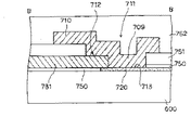
図1は本発明の一実施形態に係る半導体装置として、TFTの平面図、図2は図1に示したTFTのA−A断面図である。なお、この実施形態に係るTFTは図11に示した回路に本発明を適用したものである。
次に、図1及び図2に示したTFTの製造方法を説明する。
次に、本発明の電気光学装置の第1の実施形態として、電荷注入型の有機薄膜EL素子を用いたアクティブマトリクス型表示装置について説明する。
次に、本発明の電気光学装置の第2の実施形態として、上記の電気光学装置とは形態の異なる電荷注入型の有機薄膜EL素子を用いたアクティブマトリクス型表示装置について説明する。
3 チャネル領域
4 ソース領域
5 ドレイン領域
6 ゲート絶縁膜
7 ゲート電極
9 層間絶縁膜
10 配線
11 コンタクトホール
12、13 接続面
310 導通部
Claims (1)
- 基板上に、複数の走査線と、該走査線の延設方向に対して交差する方向に延設された複数のデータ線と、該データ線に並列する複数の共通給電線と、前記データ線と前記走査線とによりマトリクス状に形成された画素領域とを有し、
該画素領域の各々には、前記走査線を介して走査信号が第1のゲート電極に供給される第1の薄膜トランジスタと、該第1の薄膜トランジスタを介して前記データ線から供給される画像信号が第2のゲート電極に供給される第2の薄膜トランジスタと、前記画素領域毎に形成された画素電極と前記走査線と前記データ線を跨いで複数の前記画素電極に対応する対向電極との層間において前記画素電極が前記第2の薄膜トラジスタを介して前記共通給電線に電気的に接続したときに前記画素電極と前記対向電極との間に流れる駆動電流によって発光する発光層を具備する発光素子とを有する電気光学装置であって、
前記第1の薄膜トランジスタの半導体層上を覆うように形成されたゲート絶縁膜と、
前記ゲート絶縁膜上に形成された前記第2のゲート電極と導通する第1の配線と、
前記第1の配線を覆うように前記ゲート絶縁膜上に形成された層間絶縁膜と、 前記層間絶縁膜上に形成された第2の配線と、
前記半導体層のソース領域又はドレイン領域と前記第1の配線と前記第2の配線とを前記ゲート絶縁膜及び前記層間絶縁膜を貫通するひとつのコンタクトホールを介して導通する導通部と
を具備することを特徴とする電気光学装置。
Priority Applications (1)
| Application Number | Priority Date | Filing Date | Title |
|---|---|---|---|
| JP2004165852A JP3985804B2 (ja) | 2004-06-03 | 2004-06-03 | 電気光学装置 |
Applications Claiming Priority (1)
| Application Number | Priority Date | Filing Date | Title |
|---|---|---|---|
| JP2004165852A JP3985804B2 (ja) | 2004-06-03 | 2004-06-03 | 電気光学装置 |
Related Parent Applications (1)
| Application Number | Title | Priority Date | Filing Date |
|---|---|---|---|
| JP16694599A Division JP3666305B2 (ja) | 1999-06-14 | 1999-06-14 | 半導体装置、電気光学装置及び半導体装置の製造方法 |
Publications (2)
| Publication Number | Publication Date |
|---|---|
| JP2004272293A JP2004272293A (ja) | 2004-09-30 |
| JP3985804B2 true JP3985804B2 (ja) | 2007-10-03 |
Family
ID=33128724
Family Applications (1)
| Application Number | Title | Priority Date | Filing Date |
|---|---|---|---|
| JP2004165852A Expired - Lifetime JP3985804B2 (ja) | 2004-06-03 | 2004-06-03 | 電気光学装置 |
Country Status (1)
| Country | Link |
|---|---|
| JP (1) | JP3985804B2 (ja) |
Families Citing this family (5)
| Publication number | Priority date | Publication date | Assignee | Title |
|---|---|---|---|---|
| JP5212683B2 (ja) * | 2007-03-20 | 2013-06-19 | カシオ計算機株式会社 | トランジスタパネル及びその製造方法 |
| JP5305646B2 (ja) * | 2007-12-18 | 2013-10-02 | 株式会社ジャパンディスプレイウェスト | 半導体装置、電気光学装置、及び電子機器 |
| KR101434366B1 (ko) | 2012-08-24 | 2014-08-26 | 삼성디스플레이 주식회사 | 박막 트랜지스터 어레이 기판, 이를 포함하는 표시 장치 |
| US10825843B2 (en) * | 2016-10-19 | 2020-11-03 | Sharp Kabushiki Kaisha | Active matrix substrate and method for producing same |
| US11289563B2 (en) * | 2017-09-28 | 2022-03-29 | Sharp Kabushiki Kaisha | Electrode contact structure, display control driver, and display device |
-
2004
- 2004-06-03 JP JP2004165852A patent/JP3985804B2/ja not_active Expired - Lifetime
Also Published As
| Publication number | Publication date |
|---|---|
| JP2004272293A (ja) | 2004-09-30 |
Similar Documents
| Publication | Publication Date | Title |
|---|---|---|
| US11264443B2 (en) | Display substrate with light shielding layer and manufacturing method thereof, and display panel | |
| JP3536301B2 (ja) | 表示装置 | |
| JP3830238B2 (ja) | アクティブマトリクス型装置 | |
| CN105280137B (zh) | 有机发光显示器及其制造方法 | |
| EP2278618B1 (en) | Organic light emitting display device and fabricating method thereof | |
| US9818969B2 (en) | Organic light emitting diode display device and method of manufacturing the same | |
| KR100696479B1 (ko) | 평판표시장치 및 그의 제조방법 | |
| WO1998012689A1 (en) | Matrix type display device and method of production thereof | |
| KR101427585B1 (ko) | 박막 트랜지스터, 박막 트랜지스터를 포함하는 표시 장치및 그 제조 방법 | |
| JP3666305B2 (ja) | 半導体装置、電気光学装置及び半導体装置の製造方法 | |
| KR20110051784A (ko) | 어레이 기판 | |
| KR20120126950A (ko) | 유기발광표시장치 및 이의 제조방법 | |
| US8461593B2 (en) | Display apparatus and method of manufacturing the same | |
| KR20060087740A (ko) | 유기 발광 표시 장치용 박막 트랜지스터 표시판 | |
| JP3985804B2 (ja) | 電気光学装置 | |
| US20080054268A1 (en) | Display device and method of manufacturing the display device | |
| US8860915B2 (en) | Display device | |
| JP3904016B2 (ja) | アクティブマトリクス型表示装置 | |
| JP3804646B2 (ja) | 表示装置 | |
| JP2003178873A (ja) | 表示素子の製造方法 | |
| JP2004177972A (ja) | アクティブマトリクス基板、及び表示装置 | |
| JP3690406B2 (ja) | 有機エレクトロルミネッセンス装置 | |
| JP3803342B2 (ja) | 有機半導体膜の形成方法、及びアクティブマトリクス基板の製造方法 | |
| JP2007095706A (ja) | 発光装置 | |
| JP2003241676A (ja) | 表示素子の製造方法及び表示素子用基板の製造方法 |
Legal Events
| Date | Code | Title | Description |
|---|---|---|---|
| RD04 | Notification of resignation of power of attorney |
Free format text: JAPANESE INTERMEDIATE CODE: A7424 Effective date: 20070402 |
|
| TRDD | Decision of grant or rejection written | ||
| A01 | Written decision to grant a patent or to grant a registration (utility model) |
Free format text: JAPANESE INTERMEDIATE CODE: A01 Effective date: 20070619 |
|
| A61 | First payment of annual fees (during grant procedure) |
Free format text: JAPANESE INTERMEDIATE CODE: A61 Effective date: 20070702 |
|
| R150 | Certificate of patent or registration of utility model |
Ref document number: 3985804 Country of ref document: JP Free format text: JAPANESE INTERMEDIATE CODE: R150 Free format text: JAPANESE INTERMEDIATE CODE: R150 |
|
| FPAY | Renewal fee payment (event date is renewal date of database) |
Free format text: PAYMENT UNTIL: 20100720 Year of fee payment: 3 |
|
| FPAY | Renewal fee payment (event date is renewal date of database) |
Free format text: PAYMENT UNTIL: 20110720 Year of fee payment: 4 |
|
| FPAY | Renewal fee payment (event date is renewal date of database) |
Free format text: PAYMENT UNTIL: 20110720 Year of fee payment: 4 |
|
| FPAY | Renewal fee payment (event date is renewal date of database) |
Free format text: PAYMENT UNTIL: 20120720 Year of fee payment: 5 |
|
| FPAY | Renewal fee payment (event date is renewal date of database) |
Free format text: PAYMENT UNTIL: 20120720 Year of fee payment: 5 |
|
| FPAY | Renewal fee payment (event date is renewal date of database) |
Free format text: PAYMENT UNTIL: 20130720 Year of fee payment: 6 |
|
| S531 | Written request for registration of change of domicile |
Free format text: JAPANESE INTERMEDIATE CODE: R313531 |
|
| R350 | Written notification of registration of transfer |
Free format text: JAPANESE INTERMEDIATE CODE: R350 |
|
| R250 | Receipt of annual fees |
Free format text: JAPANESE INTERMEDIATE CODE: R250 |
|
| EXPY | Cancellation because of completion of term |