JP3910315B2 - Liquid crystal display - Google Patents
Liquid crystal display Download PDFInfo
- Publication number
- JP3910315B2 JP3910315B2 JP23016499A JP23016499A JP3910315B2 JP 3910315 B2 JP3910315 B2 JP 3910315B2 JP 23016499 A JP23016499 A JP 23016499A JP 23016499 A JP23016499 A JP 23016499A JP 3910315 B2 JP3910315 B2 JP 3910315B2
- Authority
- JP
- Japan
- Prior art keywords
- layer
- signal
- liquid crystal
- substrate
- resistor
- Prior art date
- Legal status (The legal status is an assumption and is not a legal conclusion. Google has not performed a legal analysis and makes no representation as to the accuracy of the status listed.)
- Expired - Fee Related
Links
Images


Classifications
-
- G—PHYSICS
- G02—OPTICS
- G02F—OPTICAL DEVICES OR ARRANGEMENTS FOR THE CONTROL OF LIGHT BY MODIFICATION OF THE OPTICAL PROPERTIES OF THE MEDIA OF THE ELEMENTS INVOLVED THEREIN; NON-LINEAR OPTICS; FREQUENCY-CHANGING OF LIGHT; OPTICAL LOGIC ELEMENTS; OPTICAL ANALOGUE/DIGITAL CONVERTERS
- G02F1/00—Devices or arrangements for the control of the intensity, colour, phase, polarisation or direction of light arriving from an independent light source, e.g. switching, gating or modulating; Non-linear optics
- G02F1/01—Devices or arrangements for the control of the intensity, colour, phase, polarisation or direction of light arriving from an independent light source, e.g. switching, gating or modulating; Non-linear optics for the control of the intensity, phase, polarisation or colour
- G02F1/13—Devices or arrangements for the control of the intensity, colour, phase, polarisation or direction of light arriving from an independent light source, e.g. switching, gating or modulating; Non-linear optics for the control of the intensity, phase, polarisation or colour based on liquid crystals, e.g. single liquid crystal display cells
- G02F1/133—Constructional arrangements; Operation of liquid crystal cells; Circuit arrangements
- G02F1/1333—Constructional arrangements; Manufacturing methods
-
- G—PHYSICS
- G06—COMPUTING; CALCULATING OR COUNTING
- G06F—ELECTRIC DIGITAL DATA PROCESSING
- G06F3/00—Input arrangements for transferring data to be processed into a form capable of being handled by the computer; Output arrangements for transferring data from processing unit to output unit, e.g. interface arrangements
- G06F3/01—Input arrangements or combined input and output arrangements for interaction between user and computer
- G06F3/03—Arrangements for converting the position or the displacement of a member into a coded form
- G06F3/041—Digitisers, e.g. for touch screens or touch pads, characterised by the transducing means
- G06F3/0412—Digitisers structurally integrated in a display
-
- G—PHYSICS
- G02—OPTICS
- G02F—OPTICAL DEVICES OR ARRANGEMENTS FOR THE CONTROL OF LIGHT BY MODIFICATION OF THE OPTICAL PROPERTIES OF THE MEDIA OF THE ELEMENTS INVOLVED THEREIN; NON-LINEAR OPTICS; FREQUENCY-CHANGING OF LIGHT; OPTICAL LOGIC ELEMENTS; OPTICAL ANALOGUE/DIGITAL CONVERTERS
- G02F1/00—Devices or arrangements for the control of the intensity, colour, phase, polarisation or direction of light arriving from an independent light source, e.g. switching, gating or modulating; Non-linear optics
- G02F1/01—Devices or arrangements for the control of the intensity, colour, phase, polarisation or direction of light arriving from an independent light source, e.g. switching, gating or modulating; Non-linear optics for the control of the intensity, phase, polarisation or colour
- G02F1/13—Devices or arrangements for the control of the intensity, colour, phase, polarisation or direction of light arriving from an independent light source, e.g. switching, gating or modulating; Non-linear optics for the control of the intensity, phase, polarisation or colour based on liquid crystals, e.g. single liquid crystal display cells
- G02F1/133—Constructional arrangements; Operation of liquid crystal cells; Circuit arrangements
- G02F1/1333—Constructional arrangements; Manufacturing methods
- G02F1/13338—Input devices, e.g. touch panels
-
- G—PHYSICS
- G06—COMPUTING; CALCULATING OR COUNTING
- G06F—ELECTRIC DIGITAL DATA PROCESSING
- G06F3/00—Input arrangements for transferring data to be processed into a form capable of being handled by the computer; Output arrangements for transferring data from processing unit to output unit, e.g. interface arrangements
- G06F3/01—Input arrangements or combined input and output arrangements for interaction between user and computer
- G06F3/03—Arrangements for converting the position or the displacement of a member into a coded form
- G06F3/041—Digitisers, e.g. for touch screens or touch pads, characterised by the transducing means
- G06F3/044—Digitisers, e.g. for touch screens or touch pads, characterised by the transducing means by capacitive means
- G06F3/0444—Digitisers, e.g. for touch screens or touch pads, characterised by the transducing means by capacitive means using a single conductive element covering the whole sensing surface, e.g. by sensing the electrical current flowing at the corners
-
- G—PHYSICS
- G06—COMPUTING; CALCULATING OR COUNTING
- G06F—ELECTRIC DIGITAL DATA PROCESSING
- G06F2203/00—Indexing scheme relating to G06F3/00 - G06F3/048
- G06F2203/041—Indexing scheme relating to G06F3/041 - G06F3/045
- G06F2203/04113—Peripheral electrode pattern in resistive digitisers, i.e. electrodes at the periphery of the resistive sheet are shaped in patterns enhancing linearity of induced field
Landscapes
- Physics & Mathematics (AREA)
- Engineering & Computer Science (AREA)
- Nonlinear Science (AREA)
- General Physics & Mathematics (AREA)
- Theoretical Computer Science (AREA)
- General Engineering & Computer Science (AREA)
- Human Computer Interaction (AREA)
- Mathematical Physics (AREA)
- Chemical & Material Sciences (AREA)
- Crystallography & Structural Chemistry (AREA)
- Optics & Photonics (AREA)
- Position Input By Displaying (AREA)
- Liquid Crystal (AREA)
- Devices For Indicating Variable Information By Combining Individual Elements (AREA)
Description
【0001】
【発明の属する技術分野】
本発明は、タッチ位置を測定する手段を用いる液晶表示装置(LCD)に関し、特に、こうしたタッチ位置測定手段がLCDの基板内に一体化されるLCDに関する。
【0002】
【従来の技術】
表面をタッチする対象物または人の位置を決定するタッチ入力システムは、様々なアプリケーションにおいて使用され、タッチ位置が高精度に決定されることを要求する。通常、これらの装置は透明であり、コンピュータ表示装置上において直接適合する。CRTまたはフラット・パネル・ディスプレイ上において適合するこうしたアドオン・タッチ・スクリーンの例は、C.Skiptonによる"You can touch this! Touch screens deliver multimedia to masses"、New Media、February 10、1997、p.39-42で見い出される。アドオン・タッチ・スクリーンは、タッチ位置を決定するために様々な方法を使用する。通常、こうしたシステムの表面は、本質的に一様な抵抗率を有する層を含み、電極が表面の縁部に接続される。電極は通常、表面よりも高い電導率の材料からなり、しばしば表面上に特定のパターンでシルク・スクリーン印刷される。位置を決定するためにしばしば使用される方法は、第1の方向に電位を印加し、次に表面を横断して、第1の方向と直交する第2の方向に電位を印加する。Shintaroらによる米国特許第3591718号、及びNakamuraらによる米国特許第4649232号で述べられるように、x及びy位置が、(絶縁層を通じて)容量結合される電圧測定用プローブを用いて決定される。人体が印加AC信号をグラウンドに短絡するので、指のタッチ位置(以下、フィンガ・タッチ位置)が、電極を通じる電流フローをモニタすることにより決定されるが、これは指との間の小キャパシタンスにより、システム内の漂遊電流が非常に小さいことを要求する。Pepper,Jrによる米国特許第4293734号は、代替アプローチについて述べており、これはi)AC信号により4辺に電力を供給し、電極電流の比によりフィンガ・タッチ位置を決定するか、ii)角部を接地し、パワーを印加されたスタイラスにより誘起される電流を、角部において測定することによる。Greniasらによる米国特許第4686332号では、間隔をあけて設けられる2つの導体プレーンを含む、アドオン・タッチ・スクリーンが述べられている。フィンガ・タッチ位置は、フィンガ・タッチによる導体プレーンのキャパシタンスの変化を検出することにより決定される。最後に、米国特許第4371746号では、抵抗性タッチ表面下に(またはそれを部分的に取り囲んで)導電材料の保護層を含むアドオン・タッチ・パネルが述べられている。アドオン・パネルの保護層は、抵抗性タッチ表面に加えられる信号と同じ振幅及び位相の信号により活動化され、抵抗性タッチ表面のグラウンドの有効キャパシタンスを本質的に低減する。
【0003】
こうしたアドオン・タッチ・スクリーンの欠点は、それらが表示ユニットの重量及びサイズを増加することであり、これはノートブック・コンピュータなどの携帯用アプリケーションで使用する際、大きな欠点となる。更に、表示装置とコンピュータとの通信には使用可能なカード・スロットや、直列または並列ポート・アダプタが必要とされる。これらの欠点は、タッチ・センサをLC表示装置内に一体化することにより、多大に軽減される。液晶表示装置、とりわけ携帯用アプリケーションに適用するため、容量性タッチ技術はそのコンパクト性及び高透過率(85%乃至90%)により、最適である。抵抗性タッチ技術は、インジウムすず酸化物(ITO)の(1つではなく)2つの層を必要とし、55%乃至75%の透過率しか有さない。
【0004】
通常、カラーLC表示装置では、ビューアの方向に向けられるガラス基板が、液晶材料に接触する内面上に設けられるカラー・フィルタを有し、カラー・フィルタ基板(CF)が縁部に沿って第2のガラス基板に接着され、これがLC表示装置をアドレス指定するための能動(または受動)マトリックスを含む。カラー・フィルタは通常、黒いマトリックス材料(クロムまたは酸化クロムなど)、顔料または染料を含むポリマ層、及び表示装置の共通電極として使用されるITO層(能動マトリックス表示装置または受動マトリックス表示装置では、ライン状にパターニングされ、表示装置をアドレス指定するために使用される)から構成される(これについては、T.Kosekiらによる"Color filter for 10.4 in. diagonal 4096-color thin-film-transistor liquid crystal displays"、IBM J.Res.Develop.Vol.36 No.1 January 1992を参照のこと)。更に、Tsutsumiらによる米国特許第5278009号で述べられるように、ITO共通電極の付着以前に透明な光感応オーバコート層が、着色領域を平坦化するためにしばしば使用される。
【0005】
LCDの上側のガラス基板(例えばカラー・フィルタを含む基板)を変更することにより、容量性センシングを用いるスタイラス入力を可能にする、2つの報告が存在する。J.H.Kimらによる刊行物"A design of the position-sensitive TFT-LCD for pen applications"、SID'97、p.87-90では、カラー・フィルタ内の導電性の黒マトリックス(BM)層が、オーバコート層によりITO共通電極から分離され、AC信号が黒マトリックスに印加される。補正抵抗がアレイの外側に形成されて、電界を線形化し、印加電界の方向(X及びY)が交互にされて、スタイラス位置がテザー・スタイラス(tethered stylus)に容量結合される電圧を測定することにより決定される。黒マトリックスへの入力信号の約半分の振幅を有する大きな信号が、ITO共通電極層上に誘起される。
【0006】
H.Ikedaらによる刊行物"A New TFT-LCD with Build-in Digitizing Function"、ISW'97、p.199-202では、スタイラス入力のための抵抗層として、ITO共通電極を使用する6.6インチVGA反射ゲストホストAMLCDが述べられている。ITO共通電極に対してDCバイアスに加え、AC信号電圧勾配がXまたはY方向に交互に印加される。各縁部に沿って、別々のAl帯状電極を使用することにより、電界の特定の線形化が達成される。帯状電極は、2.5mmの中心上の幅0.25mm×長さ1mmのITO抵抗器により、能動領域に接続される。Alの抵抗率は、過度な電力消費無しに、最善の線形化のために調整される。電界がテザー・スタイラスから容量的に測定され、表示装置上の典型的な位置に対して予め測定され、コンピュータに記憶されたデータを用いて、位置が決定される。
【0007】
これらの一体化構造のいずれも、LCDの基板と人体の一部(指やつま先など)との接触位置を測定するには適切でない。なぜなら、信号層とITO共通電極間(Kimら)、または薄膜トランジスタ(TFT)アレイ内の配線(Ikedaら)間の容量結合(すなわち有効キャパシタンス)が、基板と人体間の容量結合(有効キャパシタンス)よりも遥かに強いからである。
【0008】
【発明が解決しようとする課題】
従って、基板と人体の一部(指やつま先など)との接触位置を測定するために好適な、LCDの基板内に一体化される構造を開発することが望まれる。
【0009】
更に、信号層の線形化を提供するために、LCDの基板に経済的に一体化されうる構造を開発することが待望される。
【0010】
【課題を解決するための手段】
従来技術の上述の問題及び関連問題が、基板上に一体化された信号層を有する液晶表示装置を提供する本発明の原理により解決される。回路が信号層に印加される信号に対する応答にもとづき、タッチ位置を導出する。少なくとも1つの抵抗器が、基板上に一体化される。抵抗器は信号層と回路との間に結合される。抵抗器は信号層と一緒に形成される。好適には、抵抗器は、信号層の抵抗を垂直方向及び水平方向に線形化する抵抗回路網の一部である。
【0011】
【発明の実施の形態】
図1は、ピクセル電極26(陰影領域)が表示装置のサブピクセル(6個示される)の下に形成される、従来の液晶表示装置の上面図である。通常、ピクセルは3つの隣接するレッド(R)、グリーン(G)、及びブルー(B)のサブピクセルにより表される(すなわち、3つの隣接するサブピクセルが、ピクセル電極26上に形成されるR、G、Bカラー・マトリックスを有する)。サブピクセルは、ゲート・ライン32(3本示される)と、データ・ライン31(4本示される)間に形成される。
【0012】
図2は、図1の従来の液晶表示装置の部分断面図である。表示装置は、ガラスなどの透明材料からなる第1の基板22(以下では底部基板として参照)、及び第2の基板24(以下では頂部基板として参照)を含む。2つの基板は互いに平行になるように、高精度に構成される。通常、基板22、24は、直径約1μm乃至20μm(通常3μm乃至5μm)を有するプラスチック製のスペーサ・ボールにより互いに分離され、それらの縁部(図示せず)において封止されて、両者間に閉じられた内部空間を画定する。第1の基板22はその上に、液晶表示装置のサブピクセルを画定するピクセル電極26のアレイを付着される。更に、電極膜を付着されない基板22上の選択領域には、ダイオードや薄膜トランジスタ(TFT)30などの半導体素子が形成される。周知のように、各サブピクセルに対して、1つ以上のTFT30が存在する。TFT30は各々、導電性ゲート・ライン32(図示せず)及び導電性データ・ライン31により制御され、これらは通常、各TFT30のソースが1つのそれぞれの電極26に電気的に接続される以外は、電極26に電気的に接続されないように、基板22上に付着される。ゲート・ライン32(図示せず)及びデータ・ライン31もまた、交差領域において、互いに電気的に絶縁される。第2の基板24は通常、カラー・マトリックス層23上に付着される。カラー・マトリックス層23では通常、R、GまたはBカラー・マトリックス材料23−2が、黒マトリックス材料23−1と交互配置される。黒マトリックス材料23−1が、TFT30、データ・ライン31及びゲート・ライン32(図示せず)の反対側に配置され、これらの要素を周辺入射光から遮断し、ピクセル領域の外側での光漏洩を防止する。カラー・マトリックス材料23−2は、ピクセル電極26の反対側に配置される。更に、共通電極28が通常、カラー・マトリックス層23上に形成される。上述のように、透明な光感応オーバコート層25が、共通電極の付着以前にカラー・マトリックス材料に付着され、着色領域を平坦化する。共通電極28は好適には、インジウムすず酸化物(ITO)や他の好適な材料などの導電材料の薄い透明層からなる。
【0013】
液晶材料36は、基板22と基板24間の空間を充填する。材料の性質は、以下で詳述するように、液晶表示装置20の動作モードに依存する。液晶表示装置の内部表面は、それぞれアライメント層38及び40により被覆され、液晶材料36の分子のための境界条件を提供する。基板22及び24の外部表面には、それぞれ光補償膜42及び44が配置され得る。最後に、それぞれの偏光膜46及び48が、補償膜42及び44上にそれぞれ付着されるか(光補償膜が使用される場合)、基板22及び24上にそれぞれ付着される(光補償膜が使用されない場合)。
【0014】
図2に示されるタイプの従来の液晶表示装置は、底部基板22の背後に配置される光源(図示せず)により照射され、頂部基板24の上方から見られる。
【0015】
サブピクセルの概略図が図3に示され、ここでは参照番号が図1及び図2と対応して、同一の意味を有する。コンデンサ111は、ピクセル電極26と共通電極28間に挟まれる液晶材料36のキャパシタンスを示す。セルは記憶コンデンサ120を含み得、これは液晶キャパシタンス111と並列なキャパシタンスを提供し、表示装置内の全ての記憶コンデンサに共通のライン121上で終端する。記憶コンデンサの別の代替設計は、ピクセル電極26とゲート・ライン32間に配置される記憶コンデンサ122である。
【0016】
しきい値電圧より低い電圧がゲート・ライン32に印加されるとき、TFT30はオフ状態となり、データ・ライン31及びピクセル電極26上の電位は互いに分離される。しきい値電圧よりも高い電圧がゲート・ライン32に印加されるとき、TFT30はオン状態(低インピーダンス状態)となり、データ・ライン31上の電圧がピクセル電極26を充電することを可能にする。データ・ライン31に印加される電圧は、ピクセル電極26に異なる電圧が印加されるように、変化し得る。ピクセル電極26に印加される電圧と、共通電極28の電圧との間の電位差は、セルの液晶分子の方位を制御する。ピクセル電極26に印加される電圧と、共通電極28の電圧との間の電位差の変化により、セルの液晶分子の方位が制御され、それにより異なる量の光が液晶を横断して透過し、光のグレー・スケールの表示を生成する。
【0017】
本発明はタッチ(及びスタイラス)入力機能を、表示装置の頂部基板24内に一体化する。こうした機能の概略図が、図4に示される。より詳細には、パターニングされ得る導電層が、頂部基板24内に一体化される。以下では信号層として参照される導電層が、頂部基板24の共通電極28から電気的に分離される。信号発生器が信号を信号層の角部に供給し、各角部に流れる電流が測定される。ユーザが人体の一部(例えば指またはつま先)または道具(例えば導電スタイラスの指示端部)により、頂部基板24に接触するとき、容量結合によりR−C網が形成され、角部から信号層を通じて接触ポイントに向けて電流が流れる。タッチ位置(すなわち接触ポイント)が、信号層の角部における電流から導出され得る。或いは、信号を信号層の角部に印加する代わりに、道具(スタイラスなど)の先端部が信号を伝え、信号層の角部の電流が測定され得る。この場合、道具の先端部が頂部基板24に接触する(または接近する)と、容量結合によりR−C網が形成され、角部に電流が流れる。道具の位置が信号層の角部の電流から導出され得る。信号層の角部の電流からタッチ位置を導出する回路の例が、Pepper,Jrによる米国特許第4293734号で述べられている。この回路は表示パネル内に一体化され得るか、信号層の角部に電気的に結合される集積回路上に提供され得る。
【0018】
本発明によれば、信号層及び保護プレーン層として示される第2の導電層が、表示装置の頂部基板24内に一体化され、タッチ入力をセンスするために使用される。非導電絶縁層が信号層と保護プレーン層間に配置される。保護プレーン層は信号層と共通電極間に配置される。図4に関連して上述したように、信号層の角部は信号により駆動され、各角部の電流が測定される。タッチ入力の位置(すなわち接触ポイント)が、信号層の角部において測定された電流から導出される。更に、保護プレーン層が信号により駆動され、それにより信号層と共通電極間の容量負荷が低減され、更に共通電極から信号層への雑音電流の容量結合を低下させるかまたは除去する。保護プレーン層に印加される信号は、信号層に印加される信号の振幅をスケーリングすることにより、または位相シフトすることにより、導出され得る。或いは、信号層に印加される信号が、保護プレーン層に印加される信号をスケーリングすることにより、または位相シフトすることにより、導出され得る。
【0019】
信号層及び保護プレーン層に対して信号を生成する回路の例が、図26に示される。説明の都合上、信号層、保護プレーン層及び共通電極が平らな表面として示される。回路は基準信号となる発振器を含む。信号層及び保護プレーン層の有効信号は、有効信号が信号層及び保護プレーン層にそれぞれ印加されるとき、整合する振幅及び位相を有するように、基準信号をスケーリングまたは位相シフトすることにより生成される。更に、信号層を駆動するために電流が要求されないことが好ましい。換言すると、指や他の人体部分などの容量負荷が信号層と接近するときだけ、電流が信号層に流れることが好ましい。信号層に対する有効信号は、信号層の角部に印加される。更に、各角部はその角部の電流フローを測定し、タッチ位置を導出するための回路を含む。こうした回路の例が、Pepper、Jrによる米国特許第4293734号で述べられている。更に、保護プレーン層に対する有効信号が、共通電極に印加される駆動信号にもとづく信号(好適には駆動信号を反転、スケーリング、または位相シフトすることによる)に加算され、共通電極から信号層への雑音電流の容量結合を低下させる。説明の都合上、図12は、信号層及び保護プレーン層の角部の1つに適用可能な回路を示す。同様の回路(または図12に示される回路の一部)が、信号を信号層及び保護プレーン層の他の角部にそれぞれ印加するために使用され、それにより信号層の角部の電流からタッチ位置を導出する。
【0020】
信号を信号層の角部に印加する代わりに、道具の先端部が信号を伝達し、信号層の角部の電流が測定されてもよい。この場合、道具の位置が信号層の角部の電流から導出される。前のケースと異なり、共通電極28からの雑音が信号層に結合することを阻止するために、保護プレーン層が接地され得る。或いは、共通電極28に印加される信号の振幅を反転またはスケーリングし、結果の信号を保護プレーン層に印加することにより、信号層に結合する共通電極28からの雑音を積極的に相殺することが有益かも知れない。しかしながら、共通電極雑音が問題とならない場合、信号層に対する負荷を最小化するために、保護プレーン層が浮遊状態に維持され得る。
【0021】
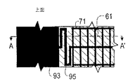
図5は、パターニングされた導電性の黒マトリックス層23−1が、信号層として使用される本発明の実施例を示す。通常通り、パターン化黒マトリックス層23−1は、頂部基板24上に形成されるカラー・マトリックス層23の一部である。パターン化導電性黒マトリックス層23−1は、クロムまたは酸化クロムか、低反射率を有し、光の透過を妨げる他の好適な材料から形成され得る。透明な非導電絶縁層61が、パターン化黒マトリックス材料23−1上に形成される。透明な非導電絶縁層61は、アクリル樹脂、ベンゾシクロブテン(BCB)または他の好適な材料などの、透明なオーバコート・ポリマから形成され得る。連続的な保護プレーン層63が、次に絶縁層61上に形成される。保護プレーン層は、ITOまたは他の好適な材料などの透明な導電材料から形成され得る。黒マトリックス層23−1と保護プレーン層63間の距離は、好適には2μm乃至5μmである。第2の透明な非導電絶縁層65が、保護プレーン層63上に形成される。第2の透明な非導電絶縁層65は、アクリル樹脂、ベンゾシクロブテンまたは他の好適な材料などの、透明なオーバコート・ポリマから形成され得る。次に、共通電極28が第2の絶縁層65上に形成される。保護プレーン層63と共通電極28間の距離は、好適には2乃至5μmである。
【0022】
図6は、パターン化導電性黒マトリックス層23−1が、保護プレーン層として使用される本発明の実施例を示す。より詳細には、信号層71が頂部基板24上に形成される。信号層71はITOなどの透明な導電材料、或いはクロムまたは酸化クロムなどの不透明な導電材料(または低反射率を有し、光の透過を妨げる他の好適な材料)から形成され得る。透明な非導電絶縁層73が、信号層71上に形成される。透明な非導電絶縁層は、アクリル樹脂、ベンゾシクロブテンまたは他の好適な材料などの、透明なオーバコート・ポリマから形成され得る。次にカラー・マトリックス層23が、絶縁層73上に形成される。通常通り、パターン化黒マトリックス層23−1は、カラー・マトリックス層23の一部である。パターン化導電性黒マトリックス層23−1は、クロムまたは酸化クロムか、低反射率を有し、光の透過を妨げる他の好適な材料から形成され得る。更に、パターン化導電性黒マトリックス層23−1は、タッチ入力のための保護プレーン層として使用される。好適には、黒マトリックス層23−1のパターニングは、信号層71のパターニングに位置合わせされる。例えば、図6に示されるように、黒マトリックス層23−1が信号層71を覆うようにパターニングされる。信号層71と黒マトリックス層23−1との距離は、好適には2μm乃至5μmである。次に、透明な非導電絶縁層75がカラー・マトリックス層23上に形成される。透明な非導電絶縁層75は、アクリル樹脂、ベンゾシクロブテンまたは他の好適な材料などの、透明なオーバコート・ポリマから形成され得る。次に、共通電極28が絶縁層75上に形成される。黒マトリックス層23と共通電極28間の距離は、好適には2μm乃至5μmである。
【0023】
好適には、頂部基板24に一体化される信号層(図5のパターン化黒マトリックス層23−1、または図6の信号層71)の縁部における抵抗は、水平(X)方向及び垂直(Y)方向の両方に線形化される。この場合、タッチ位置(すなわち接触ポイント)の位置(X、Y)は、角部において測定される電流の比から正確に導出され得る。
【数1】
X=(W/2)・{(I2+I3)(I1+I4)}/(I1+I2+I3+I4)
【数2】
Y=(H/2)・{(I1+I2)(I3+I4)}/(I1+I2+I3+I4)
【0024】
これらの単純な式は、信号層の縁部の抵抗が"線形化"される場合に、最も正確である。すなわち、上の2つの角部が正の電圧により駆動され、下の2つの角部が接地される場合、等電位は等間隔のまっすぐな水平線であるべきである。同様に、左側の2つの角部が駆動され、右側の2つの角部が接地される場合、等電位は等間隔の垂直線でなければならない。この要求は基本回路理論から導出され得る。信号層の線形化は、抵抗回路網をパターン化導電層の周囲に結合することにより達成され、それにより、パターン化導電層の抵抗がX、Y両方向において線形となるように、抵抗回路網の抵抗値(すなわち抵抗器の幾何)が変化する。一例が図7に示され、そこでは帯状抵抗201がパターン化導電層203の4辺の各々に沿って配置される。たくさんの抵抗器205が図示のように、帯状抵抗201とパターン化導電層203との間の接続を提供する。更に、抵抗器207が図示のように、帯状抵抗101と四隅のノードA、B、C、Dとの間の接続を提供する。線形化される抵抗回路網の抵抗値を決定する一般的な方法を次に示す。
【0025】
図8乃至図15は、抵抗回路網が図6に示される頂部基板24に一体化される実施例を示す。より詳細には、最初に頂部基板24上にパターン化層81を付着することにより、帯状抵抗201及び抵抗器205が形成される。パターン化層81は、ITOなどの透明な導電材料か、クロムまたは酸化クロム(若しくは低反射率を有し、光の透過を妨げる他の好適な材料)などの不透明な導電材料である。図8及び図9に示されるように、パターン化層81は好適には、帯状抵抗201を画定する帯状領域83と、抵抗回路網の抵抗器205を画定する蛇行領域85(その1つが示される)とを形成するために、パターニングされる。蛇行領域85は帯状領域83をパターン化信号層71に導電結合する。パターン化層81は図示のように、図6のパターン化信号層71と一緒に付着され、パターニングされ得る。
【0026】
パターン化層81の付着後、図10及び図11に示されるように、透明な非導電絶縁層87が好適には付着され、パターニングされる。絶縁層87は、アクリル樹脂またはベンゾシクロブテンなどの透明なポリマである。絶縁層87が光感応材料から形成される場合、パターニングは光感応材料の露光及び現像により達成される。或いは、通常のフォトリソグラフィ/エッチング技術が、絶縁層87をパターニングするために使用され得る。絶縁層87は図示のように、好適には導電層81の蛇行領域85を部分的に覆うようにパターニングされる。更に、絶縁層87は図示のように、図6の絶縁層73の一部として付着され、パターニングされる。
【0027】
絶縁層87の付着後、図12及び図13に示されるように、黒マトリックス(BM)層89が付着され、パターニングされる。好適には、黒マトリックス層89はクロム及び酸化クロムの複合含有層であり、最初に酸化クロムが付着される。それにより、背後から見られるとき、黒マトリックス層89ができる限り黒くなり、それにより表示装置から反射される光の量が低減し、表示コントラスト比が増加する。黒マトリックス層89は光の十分な吸収を提供し、本質的に光は黒マトリックス層89を透過することができない。黒マトリックス層89は好適には、導電層81の蛇行領域85を部分的に覆うようにパターニングされるが、図示のように、絶縁層87により蛇行領域85から電気的に分離される。更に、黒マトリックス層89は、図示のように、好適にはパターン化層81の帯状領域83上に直接形成されるように、パターニングされる。この複合層(黒マトリックス層89及び帯状領域83)が、帯状抵抗201を形成する上で有益な低抵抗層を形成する。更に、黒マトリックス層89は、図示のように、好適には図6の黒マトリックス材料23−1と一緒に付着され、パターニングされる。パネルのアレイ領域では、黒マトリックス材料23−1のパターニングは、ITOピクセル電極領域を除き、光の透過を遮るように設計される。ピクセル電極領域では、能動マトリックスが液晶にかかる印加電圧を制御し、正しいグレースケールを選択する。
【0028】
黒マトリックス層89の付着後、図14及び図15に示されるように、図6のカラー・フィルタ材料23−2(レッド、グリーン、ブルー要素を含む)、絶縁層75及び共通電極28が付着され、パターニングされる。
【0029】
図16乃至図23は、抵抗回路網が図5に示される頂部基板24内に一体化される実施例を示す。より詳細には、最初にパターン化層91を頂部基板24上に付着することにより、帯状抵抗201及び抵抗器205が形成される。パターン化層91は、クロムまたは酸化クロム(若しくは低反射率を有し、光の透過を妨げる他の好適な材料)などの不透明な導電材料である。図16及び図17に示されるように、パターン化層91は好適には、帯状抵抗201を画定する帯状領域93と、抵抗回路網の抵抗器205を画定する蛇行領域95(その1つが示される)とを形成するために、パターニングされる。蛇行領域95は、帯状領域83をパターン化信号層(図5の黒マトリックス層23−1)に導電結合する。パターン化層91は図示のように、図5のパターン化黒マトリックス材料23−1と一緒に付着され、パターニングされ得る。更に、図示のように、黒マトリックス材料23−1と共に、図5のカラー・フィルタ材料23−2(レッド、グリーン、ブルー要素を含む)が一般に付着され、パターニングされる。更に、黒マトリックス材料(図示せず)の追加の層が、帯状領域93上に直接形成されるように付着されて、パターニングされ、帯状抵抗201を形成する上で有益な低抵抗層を形成する。
【0030】
パターン化層91の付着後、図18及び図19に示されるように、透明な非導電絶縁層61が好適には付着され、パターニングされる。絶縁層61は、アクリル樹脂またはベンゾシクロブテンなどの透明なポリマである。絶縁層61が光感応材料から形成される場合、パターニングは光感応材料の露光及び現像により達成される。或いは、通常のフォトリソグラフィ/エッチング技術が、絶縁層61をパターニングするために使用され得る。絶縁層61は図示のように、好適には図5の絶縁層61と共に付着され、パターニングされる。
【0031】
絶縁層61の付着後、図20及び図21に示されるように、保護プレーン層63が絶縁層61上に形成される。図5に関連して上述したように、保護プレーン層63は、ITOまたは他の好適な材料などの透明な導電材料から形成され、黒マトリックス材料23−1と共通電極28との間に配置される。
【0032】
保護プレーン層63の付着後、図22及び図23に示されるように、図5の透明な非導電絶縁層65及び共通電極28が付着され、パターニングされる。
【0033】
図8乃至図15及び図16乃至図23に関連して述べた両方の実施例では、パネルの各角部において、帯状抵抗201と電気コンタクトの間に角部抵抗器207が形成される。角部抵抗器207は好適には、帯状抵抗201の形成に関して上述したのと同一のプロセスを用いて形成される。電気コンタクトは、角部から流れる電流を測定することにより、タッチ入力の位置(すなわち接触ポイント)を導出する回路に導電結合される。更に、保護プレーン層との電気コンタクトが各角部に形成される。保護プレーン層との電気コンタクトは、上述のように保護プレーンを駆動することにより、共通電極とパターン化導電層との間の容量結合を制限する回路に導電結合される。
【0034】
上述のように、帯状抵抗201及び抵抗器205が、液晶表示システムの信号層及び他の要素を形成するプロセス・ステップに関連して、頂部基板上に一体的に形成される。このアプローチは、帯状抵抗201及び抵抗器205を形成するために、追加のプロセス・ステップが要求されないために、経済的に有利である。
【0035】
信号層の抵抗を線形化する方法について、次に述べる。最初に、両方向に一様な面積抵抗率Rho_s(Ω/平方)を有する、正方形画面のための抵抗器を計算することから開始し、次にその結果を、水平及び垂直方向に異なる抵抗率を有する長方形画面に変形することにする。
【0036】
図24は、正方形画面の構成をより詳細に示す。対称性により、各縁部は同一の抵抗値を有する。タッチ検出の実際の動作では、4隅の電極が同一のAC信号により駆動されるが、縁部抵抗値を決定するために、上下の角部が対称的なDC電圧により駆動される場合について考察し(例えば上隅が+1ボルト、下隅が−1ボルトで駆動される)、抵抗層の電流及び電圧について考察することが容易である。図24の定義は、次の表のように提供される。
【表1】
記号 定義
n フィード抵抗器の数
Rho_s 画面面積抵抗率(Ω/平方)
Rs 一方の辺から他の辺への画面抵抗(Ω)、Rho_sに等しい
Re 長辺抵抗器
Rc 角部抵抗器
Ri フィード抵抗器(i=1..n)
Vs 図示のように印加されるAC印加電圧
Vm 画面の隅のAC電圧
Vi 上部のReに沿う電圧
【0037】
抵抗器Riは側部に沿って等間隔に配置されると仮定し、画面の中心において対称的であり、従ってRi=Rn+1−iである。nの値が小さい所では、画面の縁部の近くにおいて、等電位にリップルが発生する。非常に大きな値では、大きなフィード抵抗が要求され、これは形成が困難である。一般に、nは製造可能な範囲内で、できる限り大きく選択されるべきである。
【0038】
画面が正しく線形化される場合、等電位は水平線であり、上から下まで等間隔である。特に、上縁部全体は角部電位+Vmであり、下縁部は−Vmであるべきである。電流密度は電界に比例し、電界は電位分布の勾配に比例する。従って、等電位が等間隔の直線の場合、電流密度は画面を横断して一定であり、上から下に垂直方向に流れる。このことは画面の側部への、または画面の側部からの電流の流入または流出が存在しないことを意味する。側部帯状抵抗Reに沿う電位変化は、画面内の電位変化に正確に合致しなければならないことが、即時結論付けられる。そうでないと、電流が側部フィード抵抗器を介して、画面内にまたは画面から流れることになる。この条件は、側部帯状抵抗Reが単位長当たり一定の抵抗を有し、RcとRe間の各接合における電圧が角部電圧Vmに等しい場合のみ、満足される。基本回路理論から、電圧VmはVs−IRcに等しく、ここでIは側部帯状抵抗を流れる電流である。電流は2Vs/(Rc+Re+Rc)に等しい。以上から、次式が成立する。
【数3】
Vm/Vs=1/(1+2Rc/Re) (1)
【0039】
次に、画面を通じて流れる総電流Isについて考えてみよう。画面は上から下に2Vmの電圧差と、抵抗Rsを有する。従って、次式が与えられる。
【数4】
I=2Vm/Rs (2)
【0040】
この電流は上部抵抗器Rc及びReを通じて流れ、次にフィード抵抗器を通じて、画面に流れ込まねばならない。対称性から、この電流の半分が各角部から流れ込まねばならない。この時、上部抵抗器Rcにおいて、0.5RcIsに相当する電圧降下が発生するので、最初の電圧V1(図24)は次のように与えられる。
【数5】
V1=Vs−0.5RcIs=Vs−RcVm/Rs (3)
【0041】
次に、上縁部に沿うViの変化を計算する。画面への電流は、両方の角部からReに沿って流れるので、電圧は中心に向かって対称的に減少する。従って、n/2個の値を計算するだけでよい。便宜上、nが偶数の整数と仮定する。各フィード抵抗器間の帯に沿う抵抗をRoとすると、Roは次式で与えられる。
【数6】
Ro=Re/(n−1) (4)
【0042】
上述のように、電流密度は一様でなければならない。従って、等間隔のフィード抵抗器の各々は、例えば次式で与えられる同一の電流を伝導しなければならない。
【数7】
If=Is/n (5)
【0043】
式(2)から、Ifは次のように表される。
【数8】
If=2Vm/nRs (6)
【0044】
帯状抵抗Reに流れる電流は、最大値0.5Isから開始し、各フィード抵抗器の後、Ifだけ減少する。これを鑑み、最初の幾つかの電圧は次のように書き表される。
【数9】
V1=Vs−RcVm/Rs(式3による) (7)
【数10】
V2=V1−(0.5Is−1If)Ro=V1−0.5RoIs+(1)RoIf (8)
【数11】
V3=V2−(0.5Is−2If)Ro=V1−1.0RoIs+(1+2)RoIf (9)
【数12】
V4=V3−(0.5Is−3If)Ro=V1−1.5RoIs+(1+2+3)RoIf (10)
【数13】
V5=V4−(0.5Is−4If)Ro=V1−2.0RoIs+(1+2+3+4)RoIf (11)
【0045】
第2項は、−0.5(i−1)とRoIfとの積として、書き表すことができる。第3項は、最初の(i−1)個の整数の総和と、RoIfとの積である。従って、i番目の電圧は、次のように書き表される。
【数14】
Vi=V1−0.5(i−1)RoIs+0.5(i)(i−1)RoIf (12)
【0046】
式(4)及び式(5)から、Viは次のように表される。
【数15】
Vi=V1−0.5(i−1)ReIs/(n−1)+0.5(i)(i−1)ReIs/n(n−1) (13)
【数16】
Vi=V1−0.5ReIs(i−1)(n−i)/n(n−1) (14)
【0047】
式(13)に式(2)、(3)及び(7)を代入することにより、次式が得られる。
【数17】
Vi=Vs−RcVm/Rs−Vm(Re/Rs)(i−1)(n−i)/n(n−1) (15)
【0048】
最後に、式(1)を用いてVsを除去すると、次のようになる。
【数18】
Vi=Vm(1+2Rc/Re)−Vm(Rc/Rs)−Vm(Re/Rs)(i−1)(n−i)/n(n−1) (16)
【数19】
Vi=Vm(1+2Rc/Re−Rc/Rs−(Re/Rs)(i−1)(n−i)/n(n−1)) (17)
【0049】
式(17)は、ViをパラメータRe、Rc、Rs及びVmに関して表現する。さて次に、フィード抵抗器Riを計算しよう。各フィード抵抗器Riは、一端において電圧Viを、他端において画面電圧Vmを有する。従って、抵抗器電流は(Vi−Vm)/Riとなる。上述のように、この電流は各抵抗器に対して同一であり、If=Is/nに等しい。従って、次のように表わすことができる。
【数20】
(Vi−Vm)/Ri=Is/n=(2Vm/Rs)/n (18)
【数21】
Ri=(Vi−Vm)nRs/2Vm (19)
【数22】
Ri=0.5nRs(2Rc/Re−Rc/Rs−(Re/Rs)(i−1)(n−i)/n(n−1)) (20)
【0050】
従って、抵抗値(Rs、Re、Rc)が与えられると、式(20)を用いて、画面を線形化するフィード抵抗値を計算することができる。
【0051】
さて次に、Re、Rc、Rsの適切な値を選択するプロシージャが必要となる。一般に、画面抵抗Rsは導電材料の選択により固定される。次に、Re及びRcの好適な値を選択することが必要である。これらの値は、外部回路への信号の効率的な転送を保証するように、式(1)の結合率Vm/Vsを最大化するように選択されるべきである。しかしながら、式の慎重な分析結果は、(Rs、Re及びRc)の全ての組み合わせが使用可能な訳でないことを示す。不正な値が選択されると、電圧(Vi−Vm)のあるものは負となる。式(17)から、最悪(最小)の電圧は、画面の中央で発生する。このVminを代用し、i=n/2を式(17)に代入すると、次式が得られる。
【数23】
Vmin=Vm(1+2Rc/Re−Rc/Rs−(Re/4Rs)(n−2)/(n−1)) (21)
【0052】
(Vmin−Vm)が0より大きくなる条件は、次のようになる。
【数24】
Vm(1+2Rc/Re)−Vm(Rc/Rs)−Vm(Re/4Rs)(n−2)/(n−1)>Vm (22)
【0053】
代数計算の後、これは次のようになる。
【数25】
2Rc/Re>(Rc/Rs)+(Re/4Rs)(n−2)/(n−1) (23)
【0054】
ここで次の2つの無次元の比率K及びAを導入すると、都合がよい。
【数26】
K=Re/2Rs (24)
【数27】
A=Vs/Vm (25)
【0055】
式(1)から、次式が成立する。
【数28】
A=1+2Rc/Re (26)
【0056】
式(23)、式(15)及び式(19)を用いて、次の関係が得られる。
【数29】
K<Kmax (27)
【数30】
Kmax=(A−1)/(A−1+0.5(n−2)/(n−1)) (28)
【数31】
Vi/Vm=A−K(A−1)−2K(i−1)(n−i)/n(n−1) (29)
【数32】
Ri=0.5nRs(Vi/Vm−1) (30)
【数33】
Re=2KRs (31)
【数34】
Rc=0.5Re(A−1) (32)
【0057】
これらの式は次のように適用される。最初に、画面材料に従い、Rsの値を選択する。次に、比率Vm/Vsの試験値を選択する。1に近い値は、結合を増大させる。比率の逆数であるAを計算し、式(27)からKmaxを計算する。Kmaxよりも約20%小さいKの値を選択する(KがKmaxに余りに近い値に選択されると、抵抗値の非常に大きな広がりが存在することになり、画面の特性が製造公差の影響を受け易くなる)。次に式(31)及び式(32)を用いて、Re及びRcの要求値を計算する。
【0058】
Reの要求値が小さ過ぎるため、通常の材料を用いて、画面の縁部付近の限られた空間内に製造できないことが起こり得る。これはReが非常に長く、狭いからである。この場合、(Vm/Vs)のもっと低い値が試行されるべきである。好適な値が見い出されると、式(20)により、フィード抵抗が計算され得る。
【0059】
一旦、正方形画面の問題が解決されると、それを図25に示されるような幅W、高さHを有する長方形画面に変形することは容易である。水平及び垂直方向の画面抵抗率を、Rh及びVh(Ω/平方)と仮定しよう。垂直方向に測定される画面抵抗をRs_vとし、水平方向に測定される画面抵抗をRs_hとしよう。その場合、次のようになる。
【数35】
Rs_v=Rv(H/W)[Ω] (33)
【数36】
Rs_h=Rh(W/H)[Ω] (34)
【0060】
次に、上部に渡って、以前に計算された抵抗値を次のように変形する。
【数37】
Re_h=Re(Rs_v/Rs)[Ω] (35)
【数38】
Rc_h=Rc(Rs_v/Rs)[Ω] (36)
【数39】
Ri_h=Ri(Rs_v/Rs)[Ω] (37)
【0061】
次に側部に沿って以前に計算された抵抗値を、次のように変形する。
【数40】
Re_v=Re(Rs_h/Rs)[Ω] (38)
【数41】
Rc_v=Rc(Rs_h/Rs)[Ω] (39)
【数42】
Ri_v=Ri(Rs_h/Rs)[Ω] (40)
【0062】
ここでは公式な証明は省略する。要するに、これは垂直方向の画面への電流フローは、上部の抵抗器を通過し、水平方向の電流フローは、側部の抵抗器を通過することによる。抵抗器の各セットを前記のように変更することにより、正方形画面において計算された電圧を保持することができる。
【0063】
有利な点として、本発明のLCDは、LCDの頂部基板上に一体化された信号層及び保護プレーン層を含み、保護プレーン層は頂部基板の信号層と共通電極との間に配置される。信号層はソース信号により駆動され、応答が測定される。保護プレーン層は、共通電極と信号層との間の容量結合を低下させる信号により駆動され、信号層に印加されるソース信号に対する測定応答にもとづき、人体の一部(指またはつま先など)の接触位置の決定が可能になる。更に、LCDの頂部基板上に信号層及び保護プレーン層を一体化することにより、アドオン・タッチ入力画面の廉価な代用品が提供される。
【0064】
或いは、道具の先端部がソース信号により駆動され、信号層上のソース信号に対する応答が測定される。頂部基板上の道具の接触位置が、ソース信号に対する測定応答にもとづき決定される。
【0065】
本発明の信号層及び保護プレーンは、能動マトリックスLCDシステムにおいて実現されるように述べてきた。しかしながら、本発明はこの点に限られるものではなく、任意の表示システムにおいて実現され得る。表示要素のマトリックスが基板の第1の側の上方から見られ、表示要素が基板の第2の側(すなわち反対側)に配置される。例えば、本発明は受動マトリックスLCDシステムにおいて実現され得る。こうしたシステムでは、TFT素子及びデータ・ラインが底部基板から省かれ、頂部基板上に形成される共通電極がパターニングされて、データ・ラインを形成する(これらは機能的には、能動マトリックス表示装置のデータ・ライン31に等価である)。サブピクセル領域のマトリックスは、底部基板のゲート・ラインと、頂部基板のパターン化データ・ラインとの交差により形成される。こうしたシステムでは、信号層及び保護プレーン層が、受動マトリックス表示装置の頂部基板内に一体化され、パターン化データ・ラインと能動マトリックス表示装置の頂部基板との間に配置され得る。
【0066】
同様に、本発明は磁気マトリックス表示システムにおいても、実現され得る(その一例が、本願の出願人に権利譲渡された、Knoxらによる1996年8月9日付けの米国特許出願第695857号で述べられている)。こうしたシステムは、電子源と対向する複数の蛍光体要素(例えば帯状蛍光体)を有する頂部ガラス基板を含む。磁気マトリックスは、電子源により生成される電子の方向を制御することにより、頂部基板の蛍光体要素を走査する。こうしたシステムでは、本発明の信号層及び保護プレーン層が、磁気マトリックス表示装置の頂部基板内に一体化され、蛍光体要素と磁気マトリックス表示装置の頂部基板との間に配置され得る。
【0067】
まとめとして、本発明の構成に関して以下の事項を開示する。
【0068】
(1)基板と、
前記基板上に一体的に配置され、印加される信号に対する応答に従いタッチ位置が導出される信号層と、
前記信号層と前記回路間に結合され、前記基板上に一体的に配置される、前記信号層と一緒に形成される少なくとも1つの抵抗器と
を含む、液晶表示装置。
(2)前記信号層が導電材料から形成され、前記抵抗器が前記信号層の前記導電材料から形成される少なくとも1つの層を含む、前記(1)記載の液晶表示装置。
(3)前記導電材料が、低反射率を有し、光の透過を阻止する光吸収材料を含む、前記(2)記載の液晶表示装置。
(4)前記光吸収材料がクロム及び酸化クロムの1つを含む、前記(4)記載の液晶表示装置。
(5)低反射率を有し、光の透過を阻止する光吸収材料を含み、前記基板上に一体的に配置されるパターン化層を含み、
前記信号層が透明な導電材料から形成され、
前記抵抗器が、前記信号層の前記透明な導電材料から形成される第1の層と、前記表示要素の前記光吸収材料から形成される第2の層とを含む、前記(1)記載の液晶表示装置。
(6)前記光吸収材料がクロム及び酸化クロムの1つを含む、前記(5)記載の液晶表示装置。
(7)前記透明な導電材料がインジウムすず酸化物を含む、前記(6)記載の液晶表示装置。
(8)前記少なくとも1つの抵抗器が、前記信号層の抵抗を垂直方向及び水平方向に線形化する抵抗回路網の一部である、前記(1)記載の液晶表示装置。
(9)前記抵抗回路網が複数の帯状抵抗と、前記帯状抵抗と前記信号層間に結合される複数の蛇行抵抗器とを含む、前記(8)記載の液晶表示装置。
【図面の簡単な説明】
【図1】従来のクロスオーバ・タイプの能動マトリックス液晶表示装置の上面図である。
【図2】図1の液晶表示装置の部分断面図(A−A)である。
【図3】図1の能動マトリックス液晶表示装置のピクセルの概略図である。
【図4】本発明のタッチ入力機能の絵図である。
【図5】パターン化信号層及び保護プレーン層が頂部の基板24内に一体化された、本発明の実施例を示す、図1の液晶表示装置の部分断面図(A−A)である。
【図6】パターン化信号層及び保護プレーン層が頂部の基板24内に一体化された、本発明の実施例を示す、図1の液晶表示装置の部分断面図(A−A)である。
【図7】本発明に従い、頂部の基板24内に抵抗回路網を一体化することにより、パターン化導電層の抵抗を水平(X)及び垂直(Y)方向に線形化する絵図である。
【図8】図6の頂部の基板を形成するために、パターン化層81及びパターン化信号層71を形成するプロセス・ステップを示す図である。
【図9】図8の基板の断面図である。
【図10】絶縁層87を付着し、パターニングするプロセス・ステップを示す図である。
【図11】図10の基板の断面図である。
【図12】黒マトリックス(BM)層89を付着し、パターニングするプロセス・ステップを示す図である。
【図13】図12の基板の断面図である。
【図14】カラー・フィルタ材料23−2、絶縁層75及び共通電極28を付着し、パターニングするプロセス・ステップを示す図である。
【図15】図14の基板の断面図である。
【図16】図5の頂部の基板を形成するために、パターン化層91及びパターン化信号層71を形成するプロセス・ステップを示す図である。
【図17】図16の基板の断面図である。
【図18】絶縁層61を付着し、パターニングするプロセス・ステップを示す図である。
【図19】図18の基板の断面図である。
【図20】保護プレーン層63を絶縁層61上に形成するプロセス・ステップを示す図である。
【図21】図20の基板の断面図である。
【図22】絶縁層65及び共通電極28を付着し、パターニングするプロセス・ステップを示す図である。
【図23】図22の基板の断面図である。
【図24】正方形の信号層の抵抗を水平(X)及び垂直(Y)方向に線形化する抵抗回路網の絵図である。
【図25】長方形の信号層の抵抗を水平(X)及び垂直(Y)方向に線形化する抵抗回路網の絵図である。
【図26】タッチ位置を導出するために、信号層及び保護層の角部に供給される信号を生成するシステムの絵図である。
【符号の説明】
20 液晶表示装置
22 第1の基板
23−1、89 黒マトリックス材料層
23−2 RGBカラー・マトリックス材料層
24 第2の基板
25 光感応オーバコート層
26 ピクセル電極
28 共通電極
30 薄膜トランジスタ(TFT)
31 データ・ライン
32 ゲート・ライン
36 液晶材料
38、40 アライメント層
42 光補償膜
44 光補償膜
46 偏光膜
48 偏光膜
61、65、73、75、87 絶縁層
63 保護プレーン層
71 信号層
81 パターン化層
83、93 帯状領域
85、95 蛇行領域
87 非導電絶縁層
111 液晶キャパシタンス
120、122 記憶コンデンサ
201 帯状抵抗
205 フィード抵抗
207 角部抵抗[0001]
BACKGROUND OF THE INVENTION
The present invention relates to a liquid crystal display (LCD) using a means for measuring a touch position, and more particularly to an LCD in which such a touch position measuring means is integrated in an LCD substrate.
[0002]
[Prior art]
Touch input systems that determine the position of an object or person that touches a surface are used in various applications and require that the touch position be determined with high accuracy. Usually these devices are transparent and fit directly on a computer display. Examples of such add-on touch screens that fit on CRT or flat panel displays are C.I. “You can touch this! Touch screens deliver multimedia to masses” by Skipton, New Media, February 10, 1997, p. Found at 39-42. Add-on touch screens use various methods to determine touch location. Typically, the surface of such a system includes a layer with an essentially uniform resistivity, with electrodes connected to the edge of the surface. The electrodes are usually made of a material with a higher conductivity than the surface and are often silk screen printed in a specific pattern on the surface. A method often used to determine the position applies a potential in a first direction and then applies a potential across the surface in a second direction orthogonal to the first direction. As described in U.S. Pat. No. 3,591,718 to Shintaro et al. And U.S. Pat. No. 4,649,232 to Nakamura et al., The x and y positions are determined using a voltage measuring probe that is capacitively coupled (through an insulating layer). Since the human body shorts the applied AC signal to ground, the finger touch position (hereinafter referred to as finger touch position) is determined by monitoring the current flow through the electrode, which is a small capacitance between the finger. Requires that the stray current in the system be very small. U.S. Pat. No. 4,293,734 by Pepper, Jr describes an alternative approach that either i) powers the four sides with an AC signal and determines the finger touch position by the ratio of electrode currents, or ii) angle By grounding the part and measuring the current induced by the stylus with power applied at the corner. U.S. Pat. No. 4,686,332 to Grenias et al. Describes an add-on touch screen that includes two spaced apart conductor planes. The finger touch position is determined by detecting a change in the capacitance of the conductor plane due to the finger touch. Finally, US Pat. No. 4,371,746 describes an add-on touch panel that includes a protective layer of conductive material beneath (or partially surrounding) a resistive touch surface. The protective layer of the add-on panel is activated by a signal of the same amplitude and phase as the signal applied to the resistive touch surface, essentially reducing the effective capacitance of the resistive touch surface ground.
[0003]
The disadvantage of these add-on touch screens is that they increase the weight and size of the display unit, which is a major drawback when used in portable applications such as notebook computers. Furthermore, communication between the display device and the computer requires an available card slot and a serial or parallel port adapter. These drawbacks are greatly reduced by integrating the touch sensor into the LC display. Capacitive touch technology is optimal due to its compactness and high transmittance (85% to 90%) for application in liquid crystal display devices, especially portable applications. Resistive touch technology requires two layers of indium tin oxide (ITO) (rather than one) and has only 55% to 75% transmission.
[0004]
Typically, in a color LC display device, a glass substrate oriented in the direction of the viewer has a color filter provided on the inner surface that contacts the liquid crystal material, and the color filter substrate (CF) is second along the edge. It is bonded to a glass substrate, which contains an active (or passive) matrix for addressing the LC display. Color filters are typically black matrix materials (such as chromium or chromium oxide), polymer layers containing pigments or dyes, and ITO layers used as common electrodes for display devices (in active or passive matrix display devices, the line (This is used to address the display device) (see T. Koseki et al. "Color filter for 10.4 in. Diagonal 4096-color thin-film-transistor liquid crystal displays ", IBM J. Res. Develop. Vol. 36 No. 1 January 1992). Further, as described in US Pat. No. 5,277,009 by Tsutsumi et al., A transparent photosensitive overcoat layer prior to the deposition of the ITO common electrode is often used to planarize the colored areas.
[0005]
There are two reports that allow stylus input using capacitive sensing by changing the glass substrate on top of the LCD (eg, the substrate containing the color filter). J. H. Publication by Kim et al. "A design of the position-sensitive TFT-LCD for pen applications", SID '97, p. In 87-90, the conductive black matrix (BM) layer in the color filter is separated from the ITO common electrode by an overcoat layer and an AC signal is applied to the black matrix. A correction resistor is formed on the outside of the array to linearize the electric field and alternate the direction of the applied electric field (X and Y) to measure the voltage at which the stylus position is capacitively coupled to the tethered stylus. Is determined by A large signal having an amplitude about half that of the input signal to the black matrix is induced on the ITO common electrode layer.
[0006]
H. Publication by Ikeda et al. "A New TFT-LCD with Build-in Digitizing Function", ISW '97, p. 199-202 describes a 6.6 inch VGA reflective guest host AMLCD using an ITO common electrode as a resistive layer for stylus input. In addition to the DC bias, an AC signal voltage gradient is alternately applied to the ITO common electrode in the X or Y direction. A specific linearization of the electric field is achieved by using separate Al strip electrodes along each edge. The strip electrode is connected to the active area by an ITO resistor of 0.25 mm width x 1 mm length on the center of 2.5 mm. The resistivity of Al is adjusted for best linearization without excessive power consumption. The electric field is capacitively measured from the tether stylus, measured against a typical position on the display device, and the position is determined using data stored in a computer.
[0007]
None of these integrated structures are suitable for measuring the contact position between the LCD substrate and a part of the human body (such as a finger or a toe). This is because the capacitive coupling (ie effective capacitance) between the signal layer and the ITO common electrode (Kim et al.) Or between the wires (Ikeda et al.) In the thin film transistor (TFT) array is more than the capacitive coupling between the substrate and the human body (effective capacitance). Because it is much stronger.
[0008]
[Problems to be solved by the invention]
Therefore, it is desirable to develop a structure integrated in the LCD substrate, which is suitable for measuring the contact position between the substrate and a part of the human body (such as a finger or a toe).
[0009]
Furthermore, it is desired to develop a structure that can be economically integrated into the LCD substrate to provide linearization of the signal layer.
[0010]
[Means for Solving the Problems]
The above-mentioned problems and related problems of the prior art are solved by the principle of the present invention which provides a liquid crystal display device having a signal layer integrated on a substrate. A circuit derives a touch position based on a response to a signal applied to the signal layer. At least one resistor is integrated on the substrate. A resistor is coupled between the signal layer and the circuit. The resistor is formed with the signal layer. Preferably, the resistor is part of a resistor network that linearizes the signal layer resistance in the vertical and horizontal directions.
[0011]
DETAILED DESCRIPTION OF THE INVENTION
FIG. 1 is a top view of a conventional liquid crystal display device in which pixel electrodes 26 (shaded areas) are formed under sub-pixels (six are shown) of the display device. Typically, a pixel is represented by three adjacent red (R), green (G), and blue (B) subpixels (ie, three adjacent subpixels are formed on the pixel electrode 26). , G, B color matrix). A sub-pixel is formed between the gate line 32 (three shown) and the data line 31 (four shown).
[0012]
FIG. 2 is a partial cross-sectional view of the conventional liquid crystal display device of FIG. The display device includes a first substrate 22 (hereinafter referred to as a bottom substrate) and a second substrate 24 (hereinafter referred to as a top substrate) made of a transparent material such as glass. The two substrates are configured with high accuracy so as to be parallel to each other. Usually, the
[0013]
The
[0014]
A conventional liquid crystal display device of the type shown in FIG. 2 is illuminated by a light source (not shown) located behind the
[0015]
A schematic diagram of the sub-pixel is shown in FIG. 3, where reference numerals correspond to FIGS. 1 and 2 and have the same meaning. The capacitor 111 indicates the capacitance of the
[0016]
When a voltage lower than the threshold voltage is applied to the
[0017]
The present invention integrates touch (and stylus) input functionality into the
[0018]
According to the present invention, a second conductive layer, shown as a signal layer and a protection plane layer, is integrated into the
[0019]
An example of a circuit for generating signals for the signal layer and the protection plane layer is shown in FIG. For convenience of explanation, the signal layer, the protective plane layer, and the common electrode are shown as flat surfaces. The circuit includes an oscillator that serves as a reference signal. The signal layer and protection plane layer valid signals are generated by scaling or phase shifting the reference signal to have matching amplitude and phase when the valid signal is applied to the signal layer and protection plane layer, respectively. . Furthermore, it is preferred that no current is required to drive the signal layer. In other words, it is preferable that a current flows through the signal layer only when a capacitive load such as a finger or other human body part approaches the signal layer. Effective signals for the signal layer are applied to the corners of the signal layer. In addition, each corner includes circuitry for measuring the current flow at that corner and deriving the touch location. An example of such a circuit is described in US Pat. No. 4,293,734 by Pepper, Jr. In addition, the valid signal for the protection plane layer is added to a signal based on the drive signal applied to the common electrode (preferably by inverting, scaling, or phase shifting the drive signal) and from the common electrode to the signal layer. Reduce capacitive coupling of noise current. For convenience of explanation, FIG. 12 shows a circuit applicable to one of the corners of the signal layer and the protection plane layer. A similar circuit (or part of the circuit shown in FIG. 12) is used to apply the signal to the other corners of the signal layer and the protection plane layer, respectively, thereby touching from the current at the corners of the signal layer. Deriving the position.
[0020]
Instead of applying a signal to the corner of the signal layer, the tip of the tool may transmit the signal and the current at the corner of the signal layer may be measured. In this case, the position of the tool is derived from the current at the corners of the signal layer. Unlike the previous case, the protective plane layer can be grounded to prevent noise from the
[0021]
FIG. 5 shows an embodiment of the present invention in which a patterned conductive black matrix layer 23-1 is used as the signal layer. As usual, the patterned black matrix layer 23-1 is a part of the
[0022]
FIG. 6 illustrates an embodiment of the present invention in which a patterned conductive black matrix layer 23-1 is used as a protective plane layer. More specifically, a
[0023]
Preferably, the resistance at the edge of the signal layer (patterned black matrix layer 23-1 in FIG. 5 or
[Expression 1]
X = (W / 2) · {(I2 + I3) (I1 + I4)} / (I1 + I2 + I3 + I4)
[Expression 2]
Y = (H / 2) · {(I1 + I2) (I3 + I4)} / (I1 + I2 + I3 + I4)
[0024]
These simple equations are most accurate when the resistance at the edge of the signal layer is "linearized". That is, if the top two corners are driven by a positive voltage and the bottom two corners are grounded, the equipotential should be an equidistant straight horizontal line. Similarly, if the two left corners are driven and the two right corners are grounded, the equipotentials must be equidistant vertical lines. This requirement can be derived from basic circuit theory. Signal layer linearization is achieved by coupling the resistor network around the patterned conductive layer, so that the resistance of the patterned conductive layer is linear in both the X and Y directions. The resistance value (ie resistor geometry) changes. An example is shown in FIG. 7, where a
[0025]
8-15 illustrate an embodiment in which a resistor network is integrated into the
[0026]
After deposition of the patterned
[0027]
After the insulating
[0028]
After deposition of the
[0029]
FIGS. 16-23 show an embodiment in which the resistor network is integrated into the
[0030]
After deposition of the patterned
[0031]
After the insulating
[0032]
After deposition of the
[0033]
In both embodiments described in connection with FIGS. 8-15 and 16-23, a
[0034]
As described above,
[0035]
A method for linearizing the resistance of the signal layer will be described next. Start by calculating a resistor for a square screen, first having a uniform area resistivity Rho_s (Ω / square) in both directions, and then the results for different horizontal and vertical resistivities. It will be transformed into a rectangular screen having.
[0036]
FIG. 24 shows the configuration of the square screen in more detail. Due to symmetry, each edge has the same resistance value. In the actual operation of touch detection, the electrodes at the four corners are driven by the same AC signal, but in order to determine the edge resistance value, the case where the upper and lower corners are driven by a symmetric DC voltage is considered. However, it is easy to consider the current and voltage of the resistive layer (for example, the upper corner is driven at +1 volt and the lower corner is -1 volt). The definition of FIG. 24 is provided as shown in the following table.
[Table 1]
Symbol Definition
n Number of feed resistors
Rho_s Screen area resistivity (Ω / square)
Rs Screen resistance (Ω) from one side to the other, equal to Rho_s
Re long side resistor
Rc corner resistor
Ri feed resistors (i = 1 ... n)
Vs AC applied voltage as shown
Vm AC voltage at the corner of the screen
Voltage along Re at the top of Vi
[0037]
The resistors Ri are assumed to be equally spaced along the side and are symmetric at the center of the screen, so Ri = Rn + 1−i. Where the value of n is small, ripples occur in the equipotential near the edge of the screen. At very large values, a large feed resistance is required, which is difficult to form. In general, n should be chosen as large as possible within the manufacturable range.
[0038]
If the screen is linearized correctly, the equipotential is a horizontal line, equidistant from top to bottom. In particular, the entire upper edge should be at the corner potential + Vm and the lower edge should be -Vm. The current density is proportional to the electric field, and the electric field is proportional to the gradient of the potential distribution. Therefore, when the equipotential is a straight line with equal intervals, the current density is constant across the screen and flows vertically from top to bottom. This means that there is no current inflow or outflow to or from the sides of the screen. It is immediately concluded that the potential change along the side strip resistor Re must exactly match the potential change in the screen. Otherwise, current will flow into or out of the screen via the side feed resistors. This condition is satisfied only when the side band resistor Re has a constant resistance per unit length and the voltage at each junction between Rc and Re is equal to the corner voltage Vm. From basic circuit theory, the voltage Vm is equal to Vs-IRc, where I is the current through the sideband resistors. The current is equal to 2Vs / (Rc + Re + Rc). From the above, the following equation is established.
[Equation 3]
Vm / Vs = 1 / (1 + 2Rc / Re) (1)
[0039]
Next, consider the total current Is flowing through the screen. The screen has a voltage difference of 2 Vm from the top to the bottom and a resistance Rs. Therefore, the following equation is given.
[Expression 4]
I = 2Vm / Rs (2)
[0040]
This current must flow through the top resistors Rc and Re and then through the feed resistor into the screen. Due to symmetry, half of this current must flow from each corner. At this time, since a voltage drop corresponding to 0.5RcIs occurs in the upper resistor Rc, the first voltage V1 (FIG. 24) is given as follows.
[Equation 5]
V1 = Vs−0.5RcIs = Vs−RcVm / Rs (3)
[0041]
Next, the change in Vi along the upper edge is calculated. Since the current to the screen flows along Re from both corners, the voltage decreases symmetrically toward the center. Therefore, it is only necessary to calculate n / 2 values. For convenience, assume that n is an even integer. If the resistance along the band between the feed resistors is Ro, Ro is given by the following equation.
[Formula 6]
Ro = Re / (n-1) (4)
[0042]
As mentioned above, the current density must be uniform. Thus, each equally spaced feed resistor must conduct the same current, for example given by:
[Expression 7]
If = Is / n (5)
[0043]
From Expression (2), If is expressed as follows.
[Equation 8]
If = 2Vm / nRs (6)
[0044]
The current flowing in the strip resistor Re starts from a maximum value of 0.5 Is and decreases by If after each feed resistor. In view of this, the first few voltages are written as:
[Equation 9]
V1 = Vs−RcVm / Rs (according to Formula 3) (7)
[Expression 10]
V2 = V1- (0.5Is-1If) Ro = V1-0.5RoIs + (1) RoIf (8)
[Expression 11]
V3 = V2- (0.5Is-2If) Ro = V1-1.0RoIs + (1 + 2) RoIf (9)
[Expression 12]
V4 = V3- (0.5Is-3If) Ro = V1-1.5RoIs + (1 + 2 + 3) RoIf (10)
[Formula 13]
V5 = V4- (0.5Is-4If) Ro = V1-2.0RoIs + (1 + 2 + 3 + 4) RoIf (11)
[0045]
The second term can be written as the product of -0.5 (i-1) and RoIf. The third term is the product of the sum of the first (i−1) integers and RoIf. Therefore, the i-th voltage is expressed as follows.
[Expression 14]
Vi = V1-0.5 (i-1) RoIs + 0.5 (i) (i-1) RoIf (12)
[0046]
From Expression (4) and Expression (5), Vi is expressed as follows.
[Expression 15]
Vi = V1-0.5 (i-1) ReIs / (n-1) +0.5 (i) (i-1) ReIs / n (n-1) (13)
[Expression 16]
Vi = V1-0.5ReIs (i-1) (ni) / n (n-1) (14)
[0047]
By substituting equations (2), (3), and (7) into equation (13), the following equation is obtained.
[Expression 17]
Vi = Vs-RcVm / Rs-Vm (Re / Rs) (i-1) (ni) / n (n-1) (15)
[0048]
Finally, removing Vs using equation (1) yields:
[Formula 18]
Vi = Vm (1 + 2Rc / Re) −Vm (Rc / Rs) −Vm (Re / Rs) (i−1) (n−i) / n (n−1) (16)
[Equation 19]
Vi = Vm (1 + 2Rc / Re-Rc / Rs- (Re / Rs) (i-1) (ni) / n (n-1)) (17)
[0049]
Equation (17) expresses Vi with respect to the parameters Re, Rc, Rs and Vm. Now let's calculate the feed resistor Ri. Each feed resistor Ri has a voltage Vi at one end and a screen voltage Vm at the other end. Therefore, the resistor current is (Vi−Vm) / Ri. As mentioned above, this current is the same for each resistor and is equal to If = Is / n. Therefore, it can be expressed as follows.
[Expression 20]
(Vi−Vm) / Ri = Is / n = (2 Vm / Rs) / n (18)
[Expression 21]
Ri = (Vi−Vm) nRs / 2Vm (19)
[Expression 22]
Ri = 0.5 nRs (2Rc / Re-Rc / Rs- (Re / Rs) (i-1) (ni) / n (n-1)) (20)
[0050]
Therefore, given resistance values (Rs, Re, Rc), the feed resistance value for linearizing the screen can be calculated using equation (20).
[0051]
Now we need a procedure to select the appropriate values for Re, Rc, Rs. In general, the screen resistance Rs is fixed by selecting a conductive material. Next, it is necessary to select suitable values for Re and Rc. These values should be selected to maximize the coupling rate Vm / Vs in equation (1) so as to ensure efficient transfer of signals to external circuitry. However, careful analysis of the formula indicates that not all combinations of (Rs, Re and Rc) are usable. If an incorrect value is selected, one with voltage (Vi-Vm) becomes negative. From equation (17), the worst (minimum) voltage occurs at the center of the screen. Substituting i = n / 2 into equation (17) by substituting this Vmin, the following equation is obtained.
[Expression 23]
Vmin = Vm (1 + 2Rc / Re-Rc / Rs- (Re / 4Rs) (n-2) / (n-1)) (21)
[0052]
The conditions for (Vmin−Vm) to be greater than 0 are as follows.
[Expression 24]
Vm (1 + 2Rc / Re) −Vm (Rc / Rs) −Vm (Re / 4Rs) (n−2) / (n−1)> Vm (22)
[0053]
After algebraic computation, this is
[Expression 25]
2Rc / Re> (Rc / Rs) + (Re / 4Rs) (n−2) / (n−1) (23)
[0054]
Here, it is convenient to introduce the following two dimensionless ratios K and A.
[Equation 26]
K = Re / 2Rs (24)
[Expression 27]
A = Vs / Vm (25)
[0055]
From the expression (1), the following expression is established.
[Expression 28]
A = 1 + 2Rc / Re (26)
[0056]
The following relationship is obtained using Expression (23), Expression (15), and Expression (19).
[Expression 29]
K <Kmax (27)
[30]
Kmax = (A-1) / (A-1 + 0.5 (n-2) / (n-1)) (28)
[31]
Vi / Vm = AK (A-1) -2K (i-1) (ni) / n (n-1) (29)
[Expression 32]
Ri = 0.5 nRs (Vi / Vm−1) (30)
[Expression 33]
Re = 2KRs (31)
[Expression 34]
Rc = 0.5Re (A-1) (32)
[0057]
These equations apply as follows. First, the value of Rs is selected according to the screen material. Next, a test value of the ratio Vm / Vs is selected. A value close to 1 increases coupling. A, which is the reciprocal of the ratio, is calculated, and Kmax is calculated from equation (27). Choose a value of K that is about 20% smaller than Kmax (if K is chosen too close to Kmax, there will be a very large spread of resistance and the screen characteristics will be affected by manufacturing tolerances. Easier to receive). Next, the required values of Re and Rc are calculated using Equation (31) and Equation (32).
[0058]
Since the required value of Re is too small, it may not be possible to manufacture in a limited space near the edge of the screen using ordinary materials. This is because Re is very long and narrow. In this case, a lower value of (Vm / Vs) should be tried. If a suitable value is found, the feed resistance can be calculated according to equation (20).
[0059]
Once the square screen problem is solved, it is easy to transform it into a rectangular screen having a width W and a height H as shown in FIG. Let us assume that the screen resistivity in the horizontal and vertical directions is Rh and Vh (Ω / square). Let the screen resistance measured in the vertical direction be Rs_v and the screen resistance measured in the horizontal direction be Rs_h. In that case:
[Expression 35]
Rs_v = Rv (H / W) [Ω] (33)
[Expression 36]
Rs_h = Rh (W / H) [Ω] (34)
[0060]
Next, over the upper part, the previously calculated resistance value is transformed as follows.
[Expression 37]
Re_h = Re (Rs_v / Rs) [Ω] (35)
[Formula 38]
Rc_h = Rc (Rs_v / Rs) [Ω] (36)
[39]
Ri_h = Ri (Rs_v / Rs) [Ω] (37)
[0061]
Next, the previously calculated resistance value along the side is transformed as follows.
[Formula 40]
Re_v = Re (Rs_h / Rs) [Ω] (38)
[Expression 41]
Rc_v = Rc (Rs_h / Rs) [Ω] (39)
[Expression 42]
Ri_v = Ri (Rs_h / Rs) [Ω] (40)
[0062]
The official proof is omitted here. In short, this is because the current flow to the screen in the vertical direction passes through the top resistor and the current flow in the horizontal direction passes through the side resistor. By changing each set of resistors as described above, the voltage calculated in the square screen can be maintained.
[0063]
Advantageously, the LCD of the present invention includes a signal layer and a protection plane layer integrated on the top substrate of the LCD, the protection plane layer being disposed between the signal layer of the top substrate and the common electrode. The signal layer is driven by the source signal and the response is measured. The protective plane layer is driven by a signal that reduces capacitive coupling between the common electrode and the signal layer, and contacts a part of the human body (such as a finger or toe) based on a measured response to a source signal applied to the signal layer The position can be determined. In addition, integrating the signal layer and the protective plane layer on the top substrate of the LCD provides an inexpensive alternative to add-on touch input screens.
[0064]
Alternatively, the tip of the tool is driven by the source signal and the response to the source signal on the signal layer is measured. The tool contact location on the top substrate is determined based on the measured response to the source signal.
[0065]
The signal layer and protection plane of the present invention have been described as implemented in an active matrix LCD system. However, the present invention is not limited to this point, and can be realized in any display system. A matrix of display elements is viewed from above the first side of the substrate and the display elements are disposed on the second side (ie, the opposite side) of the substrate. For example, the present invention can be implemented in a passive matrix LCD system. In such a system, the TFT elements and data lines are omitted from the bottom substrate, and the common electrodes formed on the top substrate are patterned to form data lines (which are functionally active matrix display devices). Equivalent to data line 31). The matrix of sub-pixel regions is formed by the intersection of the bottom substrate gate lines and the top substrate patterned data lines. In such a system, the signal layer and the protective plane layer can be integrated into the top substrate of the passive matrix display and placed between the patterned data lines and the top substrate of the active matrix display.
[0066]
Similarly, the present invention may be implemented in a magnetic matrix display system (an example of which is described in US Patent Application No. 695857, Aug. 9, 1996 by Knox et al., Assigned to the assignee of the present application). Is). Such a system includes a top glass substrate having a plurality of phosphor elements (e.g., strip-shaped phosphors) facing an electron source. The magnetic matrix scans the phosphor elements on the top substrate by controlling the direction of electrons generated by the electron source. In such a system, the signal layer and the protective plane layer of the present invention can be integrated into the top substrate of the magnetic matrix display and placed between the phosphor element and the top substrate of the magnetic matrix display.
[0067]
In summary, the following matters are disclosed regarding the configuration of the present invention.
[0068]
(1) a substrate;
A signal layer disposed integrally on the substrate and from which a touch position is derived according to a response to the applied signal;
At least one resistor coupled with the signal layer coupled between the signal layer and the circuit and integrally disposed on the substrate;
A liquid crystal display device.
(2) The liquid crystal display device according to (1), wherein the signal layer is formed of a conductive material, and the resistor includes at least one layer formed of the conductive material of the signal layer.
(3) The liquid crystal display device according to (2), wherein the conductive material includes a light-absorbing material that has a low reflectance and prevents light transmission.
(4) The liquid crystal display device according to (4), wherein the light absorbing material includes one of chromium and chromium oxide.
(5) a light-absorbing material that has low reflectivity and prevents light transmission, and includes a patterned layer that is integrally disposed on the substrate;
The signal layer is formed of a transparent conductive material;
The resistor according to (1), wherein the resistor includes a first layer formed of the transparent conductive material of the signal layer, and a second layer formed of the light absorbing material of the display element. Liquid crystal display device.
(6) The liquid crystal display device according to (5), wherein the light absorbing material includes one of chromium and chromium oxide.
(7) The liquid crystal display device according to (6), wherein the transparent conductive material contains indium tin oxide.
(8) The liquid crystal display device according to (1), wherein the at least one resistor is part of a resistor network that linearizes the resistance of the signal layer in a vertical direction and a horizontal direction.
(9) The liquid crystal display device according to (8), wherein the resistance network includes a plurality of strip resistors and a plurality of meandering resistors coupled between the strip resistors and the signal layer.
[Brief description of the drawings]
FIG. 1 is a top view of a conventional crossover type active matrix liquid crystal display device.
2 is a partial cross-sectional view (AA) of the liquid crystal display device of FIG. 1. FIG.
FIG. 3 is a schematic diagram of pixels of the active matrix liquid crystal display device of FIG. 1;
FIG. 4 is a pictorial diagram of the touch input function of the present invention.
5 is a partial cross-sectional view (AA) of the liquid crystal display device of FIG. 1 showing an embodiment of the present invention in which a patterned signal layer and a protective plane layer are integrated into a
6 is a partial cross-sectional view (AA) of the liquid crystal display device of FIG. 1, showing an embodiment of the present invention in which a patterned signal layer and a protective plane layer are integrated into the
FIG. 7 is a pictorial diagram that linearizes the resistance of a patterned conductive layer in the horizontal (X) and vertical (Y) directions by integrating a resistor network within the
8 illustrates process steps for forming a patterned
9 is a cross-sectional view of the substrate of FIG.
FIG. 10 illustrates process steps for depositing and patterning an insulating
11 is a cross-sectional view of the substrate of FIG.
FIG. 12 illustrates the process steps for depositing and patterning a black matrix (BM)
13 is a cross-sectional view of the substrate of FIG.
FIG. 14 illustrates process steps for depositing and patterning color filter material 23-2, insulating
15 is a cross-sectional view of the substrate of FIG.
16 shows process steps for forming patterned
17 is a cross-sectional view of the substrate of FIG.
FIG. 18 illustrates process steps for depositing and patterning an insulating
19 is a cross-sectional view of the substrate of FIG.
20 is a diagram showing process steps for forming a
21 is a cross-sectional view of the substrate of FIG.
22 illustrates process steps for depositing and patterning an insulating
23 is a cross-sectional view of the substrate of FIG.
FIG. 24 is a pictorial diagram of a resistor network that linearizes the resistance of a square signal layer in the horizontal (X) and vertical (Y) directions.
FIG. 25 is a pictorial diagram of a resistor network that linearizes the resistance of a rectangular signal layer in the horizontal (X) and vertical (Y) directions.
FIG. 26 is a pictorial diagram of a system that generates signals supplied to the corners of a signal layer and a protective layer to derive a touch position.
[Explanation of symbols]
20 Liquid crystal display devices
22 First substrate
23-1, 89 Black matrix material layer
23-2 RGB color matrix material layer
24 Second substrate
25 Light sensitive overcoat layer
26 Pixel electrode
28 Common electrode
30 Thin film transistor (TFT)
31 data lines
32 Gate line
36 Liquid crystal materials
38, 40 Alignment layer
42 Optical compensation film
44 Optical compensation film
46 Polarizing film
48 Polarizing film
61, 65, 73, 75, 87 Insulating layer
63 Protection plane layer
71 Signal layer
81 Patterned layer
83, 93 Banded area
85, 95 Meander area
87 Non-conductive insulating layer
111 Liquid crystal capacitance
120, 122 storage capacitor
201 Strip resistance
205 Feed resistance
207 Corner resistance
Claims (5)
前記第2の基板上に一体的に配置され、印加される信号に対する応答に従いタッチ位置を導出するために設けられる透明な導電材料からなる信号層と、
前記信号層と、印加される信号に対する応答に従いタッチ位置を導出する回路との間に結合され、前記第2の基板上に一体的に配置される抵抗器と、
前記信号層のパターニングに位置合わせされるようにパターニングされ、前記第2の基板上に絶縁層を介して配置される、光の透過を阻止する光吸収材料から形成される低反射率を有する黒マトリックス層を含み、
前記抵抗器が、前記信号層と同じ材料で一緒に形成される第1の層と、前記黒マトリックス層と同じ材料で一緒に形成され、前記第1の層上に直接形成される第2の層とを含む、液晶表示装置。 In a liquid crystal display device in which a liquid crystal material is filled between a first substrate and a second substrate on which a black matrix layer is formed ,
A signal layer made of a transparent conductive material integrally disposed on the second substrate and provided to derive a touch position according to a response to an applied signal;
A resistor coupled between the signal layer and a circuit for deriving a touch position according to a response to an applied signal , and disposed integrally on the second substrate;
Black having a low reflectance formed from a light-absorbing material, which is patterned to be aligned with the patterning of the signal layer, and disposed on the second substrate via an insulating layer that blocks light transmission. Including a matrix layer ,
A first layer formed of the same material as the signal layer and a second layer formed of the same material as the black matrix layer and formed directly on the first layer; And a liquid crystal display device.
Applications Claiming Priority (2)
| Application Number | Priority Date | Filing Date | Title |
|---|---|---|---|
| US09/135586 | 1998-08-18 | ||
| US09/135,586 US6204897B1 (en) | 1998-08-18 | 1998-08-18 | Integrated resistor for measuring touch position in a liquid crystal display device |
Publications (2)
| Publication Number | Publication Date |
|---|---|
| JP2000089911A JP2000089911A (en) | 2000-03-31 |
| JP3910315B2 true JP3910315B2 (en) | 2007-04-25 |
Family
ID=22468731
Family Applications (1)
| Application Number | Title | Priority Date | Filing Date |
|---|---|---|---|
| JP23016499A Expired - Fee Related JP3910315B2 (en) | 1998-08-18 | 1999-08-17 | Liquid crystal display |
Country Status (5)
| Country | Link |
|---|---|
| US (1) | US6204897B1 (en) |
| JP (1) | JP3910315B2 (en) |
| KR (1) | KR100347738B1 (en) |
| CN (1) | CN1115586C (en) |
| TW (1) | TW499593B (en) |
Families Citing this family (82)
| Publication number | Priority date | Publication date | Assignee | Title |
|---|---|---|---|---|
| US7663607B2 (en) | 2004-05-06 | 2010-02-16 | Apple Inc. | Multipoint touchscreen |
| KR100473592B1 (en) * | 1999-07-19 | 2005-03-07 | 엘지.필립스 엘시디 주식회사 | A digitizer |
| JP2001075074A (en) * | 1999-08-18 | 2001-03-23 | Internatl Business Mach Corp <Ibm> | Touch sensor type liquid crystal display device |
| JP3697173B2 (en) * | 2000-05-25 | 2005-09-21 | セイコーエプソン株式会社 | Liquid crystal device and electronic device |
| JP3767499B2 (en) * | 2002-03-05 | 2006-04-19 | セイコーエプソン株式会社 | LIQUID CRYSTAL PANEL SUBSTRATE AND ITS MANUFACTURING METHOD, LIQUID CRYSTAL DISPLAY PANEL AND ELECTRONIC DEVICE |
| GB0213237D0 (en) * | 2002-06-07 | 2002-07-17 | Koninkl Philips Electronics Nv | Input system |
| US7463246B2 (en) * | 2002-06-25 | 2008-12-09 | Synaptics Incorporated | Capacitive sensing device |
| US7583250B2 (en) | 2003-03-12 | 2009-09-01 | Semiconductor Energy Laboratory Co., Ltd. | Semiconductor device |
| JP4089631B2 (en) * | 2003-09-16 | 2008-05-28 | ソニー株式会社 | Liquid crystal display device and manufacturing method thereof |
| KR100970958B1 (en) * | 2003-11-04 | 2010-07-20 | 삼성전자주식회사 | Liquid crystal display device having a touch screen function and manufacturing method thereof |
| JP3657595B1 (en) * | 2003-11-28 | 2005-06-08 | シャープ株式会社 | Display system |
| US20050174335A1 (en) * | 2004-02-10 | 2005-08-11 | Elo Touchsystems, Inc. | Resistive touchscreen with programmable display coversheet |
| US20060250533A1 (en) * | 2005-05-03 | 2006-11-09 | Po-Sheng Shih | Pixel structure with improved viewing angle |
| US20070091218A1 (en) * | 2005-10-25 | 2007-04-26 | Chin-Hai Huang | Electrostatic discharge protection structure and thin film transistor substrate including the same |
| KR100778329B1 (en) * | 2006-01-19 | 2007-11-22 | 주식회사 이에스에스디 | How to configure touch switch for light emission |
| US8144115B2 (en) * | 2006-03-17 | 2012-03-27 | Konicek Jeffrey C | Flat panel display screen operable for touch position determination system and methods |
| US7859526B2 (en) * | 2006-05-01 | 2010-12-28 | Konicek Jeffrey C | Active matrix emissive display and optical scanner system, methods and applications |
| CN104965621B (en) | 2006-06-09 | 2018-06-12 | 苹果公司 | Touch screen LCD and its operating method |
| US8243027B2 (en) * | 2006-06-09 | 2012-08-14 | Apple Inc. | Touch screen liquid crystal display |
| KR101239019B1 (en) | 2006-06-09 | 2013-03-04 | 애플 인크. | Touch screen liquid crystal display |
| US20070283832A1 (en) * | 2006-06-09 | 2007-12-13 | Apple Computer, Inc. | Imprint circuit patterning |
| US8493330B2 (en) | 2007-01-03 | 2013-07-23 | Apple Inc. | Individual channel phase delay scheme |
| US7812827B2 (en) | 2007-01-03 | 2010-10-12 | Apple Inc. | Simultaneous sensing arrangement |
| US9710095B2 (en) | 2007-01-05 | 2017-07-18 | Apple Inc. | Touch screen stack-ups |
| US8493331B2 (en) | 2007-06-13 | 2013-07-23 | Apple Inc. | Touch detection using multiple simultaneous frequencies |
| US20090174676A1 (en) | 2008-01-04 | 2009-07-09 | Apple Inc. | Motion component dominance factors for motion locking of touch sensor data |
| JP5206250B2 (en) * | 2008-05-02 | 2013-06-12 | セイコーエプソン株式会社 | Display device and electronic device |
| US8508495B2 (en) | 2008-07-03 | 2013-08-13 | Apple Inc. | Display with dual-function capacitive elements |
| US8147975B2 (en) * | 2008-08-21 | 2012-04-03 | Guardian Industries Corp. | Plasma display panel including frameless EMI filter, and/or method of making the same |
| US8592059B2 (en) * | 2008-08-21 | 2013-11-26 | Guardian Industries Corp. | Plasma display panel including EMI filter, and/or method of making the same |
| US9606663B2 (en) | 2008-09-10 | 2017-03-28 | Apple Inc. | Multiple stimulation phase determination |
| US9348451B2 (en) | 2008-09-10 | 2016-05-24 | Apple Inc. | Channel scan architecture for multiple stimulus multi-touch sensor panels |
| US8592697B2 (en) | 2008-09-10 | 2013-11-26 | Apple Inc. | Single-chip multi-stimulus sensor controller |
| US8373667B2 (en) * | 2008-11-05 | 2013-02-12 | Massachusetts Institute Of Technology | Flat panel display with capacitance sensing touch screen |
| US8144295B2 (en) | 2008-11-18 | 2012-03-27 | Apple Inc. | Common bus design for a TFT-LCD display |
| US8080141B2 (en) | 2008-11-18 | 2011-12-20 | Guardian Industries Corp. | ITO-coated article and/or method of making the same via heat treating |
| US8749496B2 (en) * | 2008-12-05 | 2014-06-10 | Apple Inc. | Integrated touch panel for a TFT display |
| US8217913B2 (en) | 2009-02-02 | 2012-07-10 | Apple Inc. | Integrated touch screen |
| US7995041B2 (en) * | 2009-02-02 | 2011-08-09 | Apple Inc. | Integrated touch screen |
| CN101488065B (en) * | 2009-03-09 | 2010-09-22 | 友达光电股份有限公司 | Touch detection method |
| TWI466004B (en) * | 2009-04-17 | 2014-12-21 | Egalax Empia Technology Inc | Method and device for resistive multi-point touch |
| US10167572B2 (en) * | 2009-08-07 | 2019-01-01 | Guardian Glass, LLC | Large area deposition of graphene via hetero-epitaxial growth, and products including the same |
| US8236118B2 (en) | 2009-08-07 | 2012-08-07 | Guardian Industries Corp. | Debonding and transfer techniques for hetero-epitaxially grown graphene, and products including the same |
| US8507797B2 (en) | 2009-08-07 | 2013-08-13 | Guardian Industries Corp. | Large area deposition and doping of graphene, and products including the same |
| US10164135B2 (en) * | 2009-08-07 | 2018-12-25 | Guardian Glass, LLC | Electronic device including graphene-based layer(s), and/or method or making the same |
| FR2949007B1 (en) | 2009-08-07 | 2012-06-08 | Nanotec Solution | DEVICE AND METHOD FOR CONTROL INTERFACE SENSITIVE TO A MOVEMENT OF A BODY OR OBJECT AND CONTROL EQUIPMENT INCORPORATING THIS DEVICE. |
| US8808810B2 (en) * | 2009-12-15 | 2014-08-19 | Guardian Industries Corp. | Large area deposition of graphene on substrates, and products including the same |
| US8460747B2 (en) | 2010-03-04 | 2013-06-11 | Guardian Industries Corp. | Large-area transparent conductive coatings including alloyed carbon nanotubes and nanowire composites, and methods of making the same |
| US8518472B2 (en) | 2010-03-04 | 2013-08-27 | Guardian Industries Corp. | Large-area transparent conductive coatings including doped carbon nanotubes and nanowire composites, and methods of making the same |
| US8604332B2 (en) * | 2010-03-04 | 2013-12-10 | Guardian Industries Corp. | Electronic devices including transparent conductive coatings including carbon nanotubes and nanowire composites, and methods of making the same |
| KR101142664B1 (en) | 2010-05-17 | 2012-05-03 | 삼성모바일디스플레이주식회사 | Liquid Crystal Display with Built-in Touch Panel and Fabricating Method Thereof |
| US8804056B2 (en) * | 2010-12-22 | 2014-08-12 | Apple Inc. | Integrated touch screens |
| JP5784959B2 (en) * | 2011-04-25 | 2015-09-24 | 富士通コンポーネント株式会社 | Touch panel |
| FR2976688B1 (en) | 2011-06-16 | 2021-04-23 | Nanotec Solution | DEVICE AND METHOD FOR GENERATING AN ELECTRICAL POWER SUPPLY IN AN ELECTRONIC SYSTEM WITH A VARIABLE REFERENCE POTENTIAL. |
| US20130005135A1 (en) | 2011-06-30 | 2013-01-03 | Guardian Industries Corp. | Planar patterned transparent contact, devices with planar patterned transparent contacts, and/or methods of making the same |
| US8747959B2 (en) | 2011-06-30 | 2014-06-10 | Guardian Industries Corp. | Planar patterned transparent contact, devices with planar patterned transparent contacts, and/or methods of making the same |
| US20130005139A1 (en) | 2011-06-30 | 2013-01-03 | Guardian Industries Corp. | Techniques for manufacturing planar patterned transparent contact and/or electronic devices including same |
| US9470941B2 (en) * | 2011-08-19 | 2016-10-18 | Apple Inc. | In-cell or on-cell touch sensor with color filter on array |
| FR2985049B1 (en) | 2011-12-22 | 2014-01-31 | Nanotec Solution | CAPACITIVE MEASURING DEVICE WITH SWITCHED ELECTRODES FOR TOUCHLESS CONTACTLESS INTERFACES |
| JP5955074B2 (en) * | 2012-04-23 | 2016-07-20 | 富士通コンポーネント株式会社 | Touch panel |
| US9395583B2 (en) | 2012-06-06 | 2016-07-19 | Apple Inc. | Column spacer design for a display incorporating a third metal layer |
| US9336723B2 (en) | 2013-02-13 | 2016-05-10 | Apple Inc. | In-cell touch for LED |
| US9593019B2 (en) | 2013-03-15 | 2017-03-14 | Guardian Industries Corp. | Methods for low-temperature graphene precipitation onto glass, and associated articles/devices |
| US10431354B2 (en) | 2013-03-15 | 2019-10-01 | Guardian Glass, LLC | Methods for direct production of graphene on dielectric substrates, and associated articles/devices |
| CN119322574A (en) | 2013-12-13 | 2025-01-17 | 苹果公司 | Integrated touch and display architecture for self-capacitive touch sensors |
| WO2015160377A1 (en) | 2014-04-16 | 2015-10-22 | Wrostix Technologies Llc | Structure for pixelated self-capacitance |
| WO2015175013A1 (en) | 2014-05-16 | 2015-11-19 | Wrostix Technologies Llc | Structure for integrated touch screen |
| WO2015178920A1 (en) | 2014-05-22 | 2015-11-26 | Onamp Research Llc | Panel bootstrapping architectures for in-cell self-capacitance |
| US9367188B2 (en) | 2014-05-23 | 2016-06-14 | Apple Inc. | RC matching in a touch screen |
| WO2015183334A1 (en) | 2014-05-28 | 2015-12-03 | Pylemta Management Llc | Narrow border touch screen |
| WO2016072983A1 (en) | 2014-11-05 | 2016-05-12 | Onamp Research Llc | Common electrode driving and compensation for pixelated self-capacitance touch screen |
| WO2016113980A1 (en) * | 2015-01-16 | 2016-07-21 | アルプス電気株式会社 | Capacitive sensor |
| AU2016215616B2 (en) | 2015-02-02 | 2018-12-06 | Apple Inc. | Flexible self-capacitance and mutual capacitance touch sensing system architecture |
| US10146359B2 (en) | 2015-04-28 | 2018-12-04 | Apple Inc. | Common electrode auto-compensation method |
| US10386962B1 (en) | 2015-08-03 | 2019-08-20 | Apple Inc. | Reducing touch node electrode coupling |
| US10145005B2 (en) | 2015-08-19 | 2018-12-04 | Guardian Glass, LLC | Techniques for low temperature direct graphene growth on glass |
| US10019090B2 (en) | 2016-03-18 | 2018-07-10 | Apple Inc. | Display with touch sensor circuitry |
| US10120520B2 (en) | 2016-07-29 | 2018-11-06 | Apple Inc. | Touch sensor panel with multi-power domain chip configuration |
| US10642418B2 (en) | 2017-04-20 | 2020-05-05 | Apple Inc. | Finger tracking in wet environment |
| US10987902B2 (en) | 2017-07-10 | 2021-04-27 | Guardian Glass, LLC | Techniques for laser ablation/scribing of coatings in pre- and post-laminated assemblies, and/or associated methods |
| US11148228B2 (en) | 2017-07-10 | 2021-10-19 | Guardian Glass, LLC | Method of making insulated glass window units |
| US11662867B1 (en) | 2020-05-30 | 2023-05-30 | Apple Inc. | Hover detection on a touch sensor panel |
Family Cites Families (8)
| Publication number | Priority date | Publication date | Assignee | Title |
|---|---|---|---|---|
| US4071691A (en) * | 1976-08-24 | 1978-01-31 | Peptek, Inc. | Human-machine interface apparatus |
| US4493104A (en) * | 1981-12-11 | 1985-01-08 | Moore Business Forms, Inc. | Character recognition device |
| US5283558A (en) * | 1989-10-16 | 1994-02-01 | Chan James K | Low-cost devices for touch control |
| DE69032091T2 (en) * | 1989-12-28 | 1998-08-20 | Gunze Kk | Input system with touch-sensitive resistance film board |
| GB9211283D0 (en) * | 1992-05-28 | 1992-07-15 | Philips Electronics Uk Ltd | Liquid crystal display devices |
| US5451724A (en) * | 1992-08-05 | 1995-09-19 | Fujitsu Limited | Touch panel for detecting a coordinate of an arbitrary position where pressure is applied |
| JP3269596B2 (en) * | 1994-10-31 | 2002-03-25 | シャープ株式会社 | Touch panel type input device |
| US5963277A (en) * | 1996-08-24 | 1999-10-05 | Lg Electronics Inc. | Position sensible liquid crystal display device |
-
1998
- 1998-08-18 US US09/135,586 patent/US6204897B1/en not_active Expired - Fee Related
-
1999
- 1999-07-13 KR KR1019990028162A patent/KR100347738B1/en not_active IP Right Cessation
- 1999-07-28 TW TW088112803A patent/TW499593B/en active
- 1999-08-04 CN CN99111899A patent/CN1115586C/en not_active Expired - Fee Related
- 1999-08-17 JP JP23016499A patent/JP3910315B2/en not_active Expired - Fee Related
Also Published As
| Publication number | Publication date |
|---|---|
| JP2000089911A (en) | 2000-03-31 |
| KR20000016925A (en) | 2000-03-25 |
| CN1245297A (en) | 2000-02-23 |
| KR100347738B1 (en) | 2002-08-09 |
| US6204897B1 (en) | 2001-03-20 |
| TW499593B (en) | 2002-08-21 |
| CN1115586C (en) | 2003-07-23 |
Similar Documents
| Publication | Publication Date | Title |
|---|---|---|
| JP3910315B2 (en) | Liquid crystal display | |
| JP3526418B2 (en) | Display cell, apparatus and method for determining contact position | |
| US7755616B2 (en) | Liquid crystal display device having electromagnetic type touch panel | |
| CN107533252B (en) | Liquid crystal display device having a plurality of pixel electrodes | |
| JP6141748B2 (en) | Display device | |
| JP4624462B2 (en) | Display device | |
| JP5164930B2 (en) | Touch panel, display panel, and display device | |
| JP5616184B2 (en) | Display device with touch detection function and electronic device | |
| US9093331B2 (en) | Liquid crystal display device having touch sensor embedded therein, method for driving the same, and method for fabricating the same | |
| US6285417B1 (en) | Position sensing liquid crystal display and method for fabricating the same | |
| JP4974670B2 (en) | Touch panel device | |
| JP6020743B1 (en) | Liquid crystal display | |
| US10884541B2 (en) | Display panel and display device | |
| KR101673206B1 (en) | Self capacitor type in-cell touch liquid crystal display device | |
| TWI641894B (en) | Liquid crystal display device and substrate for display device | |
| TWI603252B (en) | Liquid crystal display device |
Legal Events
| Date | Code | Title | Description |
|---|---|---|---|
| A02 | Decision of refusal |
Free format text: JAPANESE INTERMEDIATE CODE: A02 Effective date: 20040106 |
|
| A521 | Request for written amendment filed |
Free format text: JAPANESE INTERMEDIATE CODE: A523 Effective date: 20040324 |
|
| A911 | Transfer to examiner for re-examination before appeal (zenchi) |
Free format text: JAPANESE INTERMEDIATE CODE: A911 Effective date: 20040423 |
|
| A912 | Re-examination (zenchi) completed and case transferred to appeal board |
Free format text: JAPANESE INTERMEDIATE CODE: A912 Effective date: 20040604 |
|
| A521 | Request for written amendment filed |
Free format text: JAPANESE INTERMEDIATE CODE: A523 Effective date: 20061117 |
|
| RD14 | Notification of resignation of power of sub attorney |
Free format text: JAPANESE INTERMEDIATE CODE: A7434 Effective date: 20070116 |
|
| A61 | First payment of annual fees (during grant procedure) |
Free format text: JAPANESE INTERMEDIATE CODE: A61 Effective date: 20070124 |
|
| R150 | Certificate of patent or registration of utility model |
Free format text: JAPANESE INTERMEDIATE CODE: R150 |
|
| LAPS | Cancellation because of no payment of annual fees |