US7463246B2 - Capacitive sensing device - Google Patents
Capacitive sensing device Download PDFInfo
- Publication number
- US7463246B2 US7463246B2 US10/407,696 US40769603A US7463246B2 US 7463246 B2 US7463246 B2 US 7463246B2 US 40769603 A US40769603 A US 40769603A US 7463246 B2 US7463246 B2 US 7463246B2
- Authority
- US
- United States
- Prior art keywords
- conductive traces
- capacitive sensing
- sensing device
- substantially transparent
- transparent substrate
- Prior art date
- Legal status (The legal status is an assumption and is not a legal conclusion. Google has not performed a legal analysis and makes no representation as to the accuracy of the status listed.)
- Expired - Lifetime, expires
Links
Images


Classifications
-
- G—PHYSICS
- G06—COMPUTING OR CALCULATING; COUNTING
- G06F—ELECTRIC DIGITAL DATA PROCESSING
- G06F3/00—Input arrangements for transferring data to be processed into a form capable of being handled by the computer; Output arrangements for transferring data from processing unit to output unit, e.g. interface arrangements
- G06F3/01—Input arrangements or combined input and output arrangements for interaction between user and computer
- G06F3/03—Arrangements for converting the position or the displacement of a member into a coded form
- G06F3/041—Digitisers, e.g. for touch screens or touch pads, characterised by the transducing means
- G06F3/044—Digitisers, e.g. for touch screens or touch pads, characterised by the transducing means by capacitive means
- G06F3/0446—Digitisers, e.g. for touch screens or touch pads, characterised by the transducing means by capacitive means using a grid-like structure of electrodes in at least two directions, e.g. using row and column electrodes
-
- G—PHYSICS
- G06—COMPUTING OR CALCULATING; COUNTING
- G06F—ELECTRIC DIGITAL DATA PROCESSING
- G06F3/00—Input arrangements for transferring data to be processed into a form capable of being handled by the computer; Output arrangements for transferring data from processing unit to output unit, e.g. interface arrangements
- G06F3/01—Input arrangements or combined input and output arrangements for interaction between user and computer
- G06F3/03—Arrangements for converting the position or the displacement of a member into a coded form
- G06F3/041—Digitisers, e.g. for touch screens or touch pads, characterised by the transducing means
- G06F3/044—Digitisers, e.g. for touch screens or touch pads, characterised by the transducing means by capacitive means
- G06F3/0445—Digitisers, e.g. for touch screens or touch pads, characterised by the transducing means by capacitive means using two or more layers of sensing electrodes, e.g. using two layers of electrodes separated by a dielectric layer
Definitions
- Computing devices have become integral tools used in a wide variety of different applications, such as in finance and commercial transactions, computer-aided design and manufacturing, health care, telecommunication, education, etc. Computing devices are finding new applications as a result of advances in hardware technology and rapid development in software technology. Furthermore, the functionality of a computing device is dramatically enhanced by coupling these types of stand-alone devices together in order to form a networking environment. Within a networking environment, computing device users may readily exchange files, share information stored on a common database, pool resources, and communicate via electronic mail (e-mail) and video teleconferencing.
- e-mail electronic mail
- Conventional computing devices provide several ways for enabling a user to input a choice or a selection. For example, a user can use one or more keys of an alphanumeric keyboard communicatively connected to the computing device in order to indicate a choice or selection. Additionally, a user can use a cursor control device communicatively connected to the computing device to indicate a choice. Also, a user can use a microphone communicatively connected to the computing device to audibly indicate a particular selection. Moreover, touch sensing technology can be used to provide an input selection to a computing device or other electronic device.
- capacitive sensing touch screens there exist capacitive sensing touch screens.
- capacitive sensing touch screens there are different sensing technologies.
- one sensing technology involves the use of a uniform resistive sheet as part of the capacitive sensing touch screen.
- uniform resistive sheet sensing technology there are disadvantages associated with this commercially available uniform resistive sheet sensing technology.
- one of the disadvantages is that when an image is shown through the uniform resistive sheet, the reduced transmittance due to the optically absorbing resistive sheet optically degrades the image. If the image is shown on a display, the display has to be operated at higher brightness to compensate, which requires more power and reduces battery life.
- Another commercially available sensing technology involves using rolled out wires attached to glass as part of a capacitive sensing touch screen.
- this commercially available sensing technology involves using rolled out wires attached to glass as part of a capacitive sensing touch screen.
- the wires of the capacitive sensing touch screen are very visible when a displayed image is viewed through it. As such, the wires can be distracting to a user.
- Another disadvantage is that the wires tend to reflect unwanted ambient light towards the user, thereby obscuring the display. Consequently, the degraded image due to the obscured display can be distracting to the user.
- the present invention may address one or more of the above issues.
- the capacitive sensing device comprises a substantially transparent substrate and a set of patterned conductive traces formed above the substantially transparent substrate. Each of the set of patterned conductive traces has a width such that the capacitive sensing device does not have to be arranged with respect to an underlying image in order to avoid deleterious obstruction of the underlying image by the set of patterned conductive traces.
- the underlying image is separate from the capacitive sensing device.
- the capacitive sensing device is separate from active components used to comprise an information display device.
- FIG. 1 is a flowchart of operations performed in accordance with an embodiment of the present invention for fabricating a capacitive sensing device.
- FIG. 2 is a flowchart of operations performed in accordance with another embodiment of the present invention for fabricating a capacitive sensing device.
- FIG. 3 is a flowchart of operations performed in accordance with an embodiment of the present invention for printing a material.
- FIG. 4 is a flowchart of operations performed in accordance with an embodiment of the present invention for a photolithography/etching process.
- FIG. 5 is a flowchart of operations performed in accordance with an embodiment of the present invention for a liftoff process.
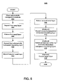
- FIG. 6 is a flowchart of operations performed in accordance with an embodiment of the present invention for manufacturing a capacitive sensing device.
- FIG. 7 is a cross sectional view of an exemplary capacitive sensing device in accordance with an embodiment of the present invention.
- FIG. 8 is a plan view of an exemplary capacitive sensing device in accordance with an embodiment of the present invention.
- FIG. 9 is a cross sectional view of an exemplary capacitive sensing device in accordance with another embodiment of the present invention.
- FIG. 10 is a top view of the capacitive sensing device of FIG. 9 in accordance with another embodiment of the present invention.
- FIG. 1 is a flowchart 100 of operations performed in accordance with an embodiment of the present invention for fabricating a capacitive sensing device. Although specific operations are disclosed in flowchart 100 , such operations are exemplary. That is, the present embodiment is well suited to performing various other operations or variations of the operations recited in FIG. 1 .
- the present embodiment provides a method for fabricating a capacitive sensing device.
- a substantially transparent substrate e.g., a glass, a plastic or a crystalline material
- a set of conductive traces is patterned above the substantially transparent substrate.
- an insulating material can be deposited above the set of conductive traces.
- the insulating material may act as protection for the set of conductive traces and also provide them electrical insulation from the outside world.
- a substantially transparent substrate is utilized to fabricate a capacitive sensing device.
- the substantially transparent substrate may include a wide variety of materials in accordance with the present embodiment.
- the substantially transparent substrate may include, but is not limited to, a glass, a plastic or a crystalline material.
- the substantially transparent substrate may be a component of an information display device.
- the substantially transparent substrate can be implemented as a part of a casing or front cover of the information display device.
- a set of conductive traces are patterned above the substantially transparent substrate.
- the set of conductive traces may be implemented in diverse ways.
- each of the set of conductive traces can have a width such that the capacitive sensing device does not have to be arranged with respect to an underlying image in order to avoid deleterious obstruction of that underlying image by the set of conductive traces.
- the underlying image is separate from the capacitive sensing device and may be displayed on an information display device.
- the underlying image is not a component of the capacitive sensing device.
- the capacitive sensing device is fabricated separately from active components of an information display device.
- the patterning of the set of conductive traces may be implemented in a wide variety of ways at operation 104 .
- the patterning of the set of conductive traces can include, but is not limited to, a lithographic process, a printing process, electron beam lithography, screen printing, inkjet printing, offset printing, electroplating, stamping, and LIGA.
- LIGA is the German abbreviation for Llthogafie Galvanoformung Abformung which in English means lithographic :electrodeposition.
- the patterning of the set of conductive traces can include patterning a landing pad region above the substantially transparent substrate to enable coupling of one or more sensing circuit components to the substantially transparent substrate.
- the landing pad region may include wiring for coupling integrated circuit (IC) chips, capacitors, resistors, connectors and other electronic components to the substantially transparent substrate.
- IC integrated circuit
- the landing pad region can be plated with gold, tin, copper or any other metal that is compatible with solder.
- many processes can be used to assemble the capacitive sensing device with its circuit components. One example would be to screen print solder paste onto the appropriate wiring pads and then place the components. The assembly can then be heated to re-flow the solder, bonding the circuit components securely to the substantially transparent substrate.
- the set of conductive traces may be implemented in diverse ways.
- the set of conductive traces can include one or more layers of material.
- the set of conductive traces can include substantially opaque material and/or substantially non-reflective material.
- the set of conductive traces can be formed of at least one layer of material that is substantially non-reflective. It is noted that by locating a substantially opaque, non-reflective material such that it faces a user of the capacitive sensing device, it can optically obscure from the user any reflective materials included as part of the set of conductive traces. In this manner, the substantially non-reflective material makes the set of conductive traces more difficult to see by the user. It is noted that the set of conductive traces can include at least one layer of substantially opaque material.
- the set of conductive traces can be patterned such that each of the conductive traces has a width less than approximately 12 micrometers. It is noted that the width of each conductive trace can be understood to mean the width of each individual conductive element of the set of conductive traces. In this manner, when a user is approximately at arm's length from the capacitive sensing device, the user's eyes are substantially unable to view the set of conductive traces of the capacitive sensing device. It is understood that by decreasing the width of each trace of the set of conductive traces, there is a point at which they are no longer resolvable by a human eye. In this fashion, there is no deleterious obstruction of an underlying image by the set of conductive traces of the capacitive sensing device.
- the set of conductive traces can be patterned at operation 104 such that each of them has a width that is substantially non-perceptible by a human user. Therefore, the set of conductive traces can be patterned such that each of them has a width such that each of them is not required to be formed of a substantially transparent material. Moreover, each of the set of conductive traces can have a width less than a pixel width of the underlying image. Also, each of the set of conductive traces can be a capacitive sensing element. It is noted that the set of conductive traces at operation 104 are not limited in any way to these different embodiments.
- an insulating material is deposited above the set of conductive traces. It is noted that the insulating material deposited at operation 106 can act as protection (e.g., from handling damage) for the set of conductive traces and also provide them electrical insulation from the outside world. As such, the deposition of the insulating material at operation 106 may be an optional operation of flowchart 100 . The deposition of the insulating material at operation 106 may be implemented in diverse ways. For example, at operation 106 , a deposition of a dielectric layer (e.g., SiO 2 , Spin-On-Glass, and the like) can be used as the insulating material.
- a dielectric layer e.g., SiO 2 , Spin-On-Glass, and the like
- the insulating material at operation 106 may include a substantially transparent insulating material or an opaque insulating material. Additionally, the insulating material may be deposited at operation 106 to cover the entire set of conductive traces or it may be deposited to cover one or more portions of the set of conductive traces. At the completion of operation 106 , the process exits flowchart 100 .
- FIG. 2 is a flowchart 200 of operations performed in accordance with an embodiment of the present invention for fabricating a capacitive sensing device. Although specific operations are disclosed in flowchart 200 , such operations are exemplary. That is, the present embodiment is well suited to performing various other operations or variations of the operations recited in FIG. 2 .
- the present embodiment provides a method for fabricating a capacitive sensing device that includes two sets of conductive traces.
- a substantially transparent substrate e.g., a glass, a plastic or a crystalline material
- a first set of conductive traces is patterned above the substantially transparent substrate.
- a first insulating material is deposited above the first set of conductive traces.
- a second set of conductive traces is patterned above and coupled to the substantially transparent substrate.
- a second insulating material can be deposited above the second set of conductive traces.
- the second insulating material may act as protection for the first and second sets of conductive traces and may also provide them electrical insulation from the outside world.
- a substantially transparent substrate is utilized to fabricate a capacitive sensing device. It is noted that the substantially transparent substrate may include a wide variety of materials in accordance with the present embodiment. It is appreciated that the substantially transparent substrate at operation 102 can be implemented in any manner similar to operation 102 of FIG. 1 , described herein.
- a first set of conductive traces are patterned above the substantially transparent substrate. It is understood that the first set of conductive traces may be implemented in diverse ways at operation 202 . For example, the first set of conductive traces can be implemented in any manner similar to the set of conductive traces at operation 104 , described herein.
- a first insulating material is deposited above the first set of conductive traces.
- the deposition of the first insulating material at operation 204 may be implemented in a wide variety of ways.
- the deposition of the first insulating material at operation 204 can be implemented in any manner similar to the deposition of the insulating material at operation 106 .
- the first insulating material at operation 204 can be implemented in any manner similar to that described herein.
- a second set of conductive traces are patterned above and coupled to the substantially transparent substrate.
- the second set of conductive traces may be implemented in diverse ways.
- the second set of conductive traces can be implemented in any manner similar to the set of conductive traces at operation 104 , described herein.
- the second set of conductive traces may provide local bridges that electrically couple traces of the first set of conductive traces as shown in FIGS. 9 and 10 .
- the second set of traces can be a second layer above the first set of conductive traces as shown in FIG. 7 .
- a second insulating material is deposited above the second set of conductive traces.
- the deposition of the second insulating material at operation 208 may be implemented in a wide variety of ways.
- the deposition of the second insulating material at operation 208 can be implemented in any manner similar to the deposition of the insulating material at operation 106 .
- the second insulating material at operation 208 can be implemented in any manner similar to that described herein. It is noted that the second insulating material deposited at operation 208 can act as protection for the second set of conductive traces and also provide them electrical insulation from the outside world.
- the second insulating material deposited at operation 208 can act as protection for the first and second sets of conductive traces and also provide them electrical insulation from the outside world.
- the deposition of the second insulating material at operation 208 may be an optional operation of flowchart 200 .
- the process exits flowchart 200 .
- any number of sets of conductive traces may be implemented in accordance with the present embodiment. For example, operations similar to operations 202 and/or 204 may be repeated as desired.
- FIGS. 3 , 4 and 5 are each a flowchart of an exemplary “patterning” operation that can be utilized in conjunction with embodiments of the present invention. It is understood that patterning can include any transference of a design to some type of surface (e.g., a substrate, a layer of material, multiple layers of material, and the like).
- FIGS. 3 , 4 and 5 each represents a process that can be utilized in combination with, but is not limited to, flowcharts 100 , 200 and 600 of FIGS. 1 , 2 and 6 , respectively. It is appreciated that FIGS. 3 , 4 and 5 each represents a process that is well known by those of ordinary skill in the art.
- FIG. 3 is a flowchart 300 of an exemplary printing process in accordance with an embodiment of the present invention. Although specific operations are disclosed in flowchart 300 , such operations are exemplary. That is, the present embodiment is well suited to performing various other operations or variations of the operations recited in FIG. 3 .
- material is deposited in a desired pattern above a substrate. It is appreciated that the deposition of the material in the desired pattern at operation 302 may be implemented in diverse ways. For example, material can be deposited in the desired pattern at operation 302 in a manner commonly referred to as a printing process that is well known by those of ordinary skill in the art. Furthermore, the deposited material may include diverse materials in accordance with the present embodiment. For example, the material may include, but is not limited to, a conductive material, a non-conductive material, an opaque material, a non-reflective material, an insulating material, a substantially transparent material and/or the like. The material at operation 302 may include one or more of the materials mentioned herein, but is not limited to such. Once operation 302 is completed, the process exits flowchart 300 .
- FIG. 4 is a flowchart 400 of an exemplary photolithography/etching process in accordance with an embodiment of the present invention. Although specific operations are disclosed in flowchart 400 , such operations are exemplary. That is, the present embodiment is well suited to performing various other operations or variations of the operations recited in FIG. 4 .
- a layer of material is deposited above a substrate. Operation 402 is performed as needed, and need not be performed if the material to be etched at operation 410 is already present prior to patterning.
- the deposition of the material at operation 402 may be implemented in a wide variety of ways. For example, the deposition of the material at operation 402 can be implemented in any manner described herein, but is not limited to such.
- the layer of material at operation 402 may include a wide variety of materials. For example, the material can include, but is not limited to, any material described herein.
- a photoresist is deposited above the layer of material.
- the photoresist is exposed to a particular pattern.
- the photoresist is developed.
- the material is etched in a manner to follow the pattern.
- the remaining photoresist is stripped, away. It is noted that operations 404 , 406 , 408 , 410 and 412 may each be implemented in a wide variety of ways that are well known by those of ordinary skill in the art.
- FIG. 5 is a flowchart 500 of an exemplary liftoff process in accordance with an embodiment of the present invention. Although specific operations are disclosed in flowchart 500 , such operations are exemplary. That is, the present embodiment is well suited to performing various other operations or variations of the operations recited in FIG. 5 .
- a layer of photoresist is deposited above a substrate.
- the deposition of the photoresist at operation 502 may be implemented in a wide variety of ways.
- the deposition of the photoresist at operation 502 can be implemented in any manner described herein, but is not limited to such.
- the photoresist is exposed to a particular pattern.
- the photoresist is developed.
- a layer of material is deposited atop the photoresist.
- the photoresist is dissolved and lifted off.
- a cleaning process is then performed. It is noted that operations 504 , 506 , 508 , 510 and 512 may each be implemented in a wide variety of ways that are well known by those of ordinary skill the art.
- FIG. 6 is a flowchart 600 of operations performed in accordance with an embodiment of the present invention for manufacturing a capacitive sensing device. Although specific operations are disclosed in flowchart 600 , such operations are exemplary. That is, the present embodiment is well suited to performing various other operations or variations of the operations recited in FIG. 6 .
- the patterning operations of flowchart 600 can be performed in diverse ways. For example, if the material to be patterned is not deposited in a separate operation, the patterning of the first metal layer can include, but is not limited to, process 300 , 400 , or 500 .
- the present embodiment provides a method for manufacturing a capacitive sensing device.
- the capacitive sensing device includes a substantially transparent substrate having two metal layers which are separated by a substantially transparent insulating layer. Additionally, a second substantially transparent insulating layer can be optionally used in order to provide an abrasion resistance layer for the second metal layer and also provide them electrical insulation from the outside world.
- Each metal layer can be patterned to provide conductive traces that can be coupled to sensory circuitry (not shown) of a capacitive sensing device.
- the first and second substantially transparent insulating layers are each patterned so that electrical contacts can be made to each of the metal layers.
- a substantially transparent substrate e.g., a glass, a plastic or a crystalline material
- a substantially transparent substrate is cleaned.
- the substantially transparent substrate is a glass
- it can be aggressively cleaned at operation 602 with, but not limited to, ultrasonic nozzles, detergents, scrubbing brushes, thorough rinse and deionized water rinses.
- the cleaning of the substantially transparent substrate is not limited to such implementations.
- a first metal layer is deposited above the substantially transparent substrate.
- the deposition of the first metal layer can be implemented in a wide variety of ways.
- the deposition of the first metal layer can be implemented utilizing, but not limited to, a sputtering process, an electron beam evaporation process or a resistive evaporation process.
- the first metal layer can include diverse materials.
- the first metal layer can include, but is not limited to, black chrome (e.g., chromium oxynitride), aluminum, titanium, nickel, chromium, and the like.
- black chrome e.g., chromium oxynitride
- aluminum titanium
- nickel chromium
- chromium a plurality of layers
- other materials and/or a plurality of layers may be incorporated as part of the first metal layer for processing or other reasons.
- a titanium layer may be included as part of the first metal layer to be utilized as an etch stop when patterning a substantially transparent insulating layer, described below.
- gold may be utilized when a liftoff process (e.g., flowchart 500 ) is used.
- gold may be utilized as part of the formation of a landing pad for sensing circuitry.
- a metal may be disposed between two other metals in the first metal layer to prevent corrosion.
- the first metal layer can include at least one layer of substantially opaque material.
- the first metal layer can be formed of at least one layer of material that is substantially non-reflective. By locating the substantially non-reflective material such that it faces a user of the capacitive sensing device, it optically obscures from the user any reflective materials included as part of the first metal layer that will eventually become conductive traces.
- the first metal layer is patterned above the substantially transparent substrate.
- the patterning of the first metal layer may be performed at operation 606 in diverse ways.
- the patterning of the first metal layer can include, but is not limited to, process 400 .
- the patterning of the first metal layer can include, but is not limited to, a lithographic process, a printing process, electron beam lithography, screen printing, inkjet printing, offset printing, electroplating, stamping, and LIGA.
- the patterning of the first metal layer can include patterning a landing pad region above the substantially transparent substrate to enable coupling of one or more sensing circuit components to the substantially transparent substrate.
- the patterning of the first metal layer at operation 606 forms a first set of conductive traces that are part of the capacitive sensing device.
- the first set of conductive traces may be implemented in diverse ways. For example, each of the first set of conductive traces can have a width such that the capacitive sensing device does not have to be arranged with respect to an underlying image in order to avoid deleterious obstruction of that underlying image by these conductive traces.
- the underlying image is separate from the capacitive sensing device.
- the capacitive sensing device is fabricated separately from active components of an information display device.
- the first set of conductive traces can also be patterned such that each of them has a width less than approximately 12 micrometers.
- the first set of conductive traces can be patterned such that each of them has a width that does not require them to be formed of a substantially transparent material.
- Each of the first set of conductive traces can also be implemented with a width less than a pixel width of the underlying image.
- each of the first set of conductive traces can be a capacitive sensing element.
- the first set of conductive traces at operation 606 is not limited in any way to these embodiments.
- a first substantially transparent insulating material layer is deposited above the first set of conductive traces and the substantially transparent substrate.
- the substantially transparent insulating layer may be implemented in diverse ways. For example, at operation 610 , a deposition of a dielectric material (e.g., SiO 2 , Spin-On-Glass, and the like) can be the first substantially transparent insulating layer.
- the first insulating layer may be deposited at operation 608 to cover and insulate the first set of conductive traces or it may be deposited to cover and insulate one or more portions of the first set of conductive traces.
- a second metal layer is deposited above the first substantially transparent insulating layer and the substantially transparent substrate. It is understood that the deposition of the second metal layer can be implemented in a wide variety of ways. For example, the deposition of the second metal layer can be implemented in any manner similar to that described herein with reference to the deposition at operation 604 of the first metal layer.
- the second metal layer is patterned above the first substantially transparent insulating layer. It is appreciated that the patterning of the second metal layer may be performed at operation 612 in diverse ways. For example, the patterning of the second metal layer can be implemented in any manner similar to that described herein with reference to the patterning at operation 606 of the first metal layer. However, it is noted that the patterning mask of the second metal layer may be different from the patterning mask of the first metal layer. Additionally, if the patterning mask for the first metal layer dictated a set of traces substantially aligned along the horizontal axis, then the patterning mask for the second metal layer can dictate a set of traces substantially aligned along the vertical axis.
- the patterning at operation 612 of the second metal layer forms a second set of conductive traces.
- the second set of conductive traces can be implemented in any manner similar to that described herein with reference to the first set of conductive traces at operation 606 .
- the second set of conductive traces can be patterned at operation 606 such that they are substantially orthogonal to the first set of conductive traces.
- a second substantially transparent insulating material layer is deposited above the second set of conductive traces and the first substantially transparent insulating layer. It is noted that the second substantially transparent insulating layer can act as a protective layer for the second set of conductive traces. Additionally, the second substantially transparent insulating layer can provide the second set of conductive traces electrical insulation from the outside world.
- the deposition of the second substantially transparent insulating layer at operation 614 can be an optional operation.
- the deposition of the second substantially transparent insulating layer at operation 614 may be implemented in diverse ways. For example, the deposition of the second substantially transparent insulating layer can be implemented in any manner similar to that described herein with reference to the deposition at operation 608 of the first substantially transparent insulating layer.
- At operation 616 of FIG. 6 at least one of the first and second substantially transparent insulating layers is patterned above portions of the first and second sets of conductive traces in order to form pads where electronics of the capacitive sensing device can be coupled to the conductive traces. Furthermore, test pads can be formed outside of the sensing area of the capacitive sensing device to enable verification of the integrity of each conductive trace. It is appreciated that the patterning of the substantially transparent insulating layer(s) at operation 616 can be implemented in a wide variety of ways. For example, the patterning of the substantially transparent insulating layer(s) at operation 616 can be implemented in any manner of patterning similar to that described herein.
- the patterning of the substantially transparent insulating layer(s) at operation 616 may include an etching process.
- an etching at operation 616 of the substantially transparent insulating layer(s) can include a wet buffered hydrogen fluoride (HF) etchant. If this etching of the substantially transparent insulating layer(s) at operation 616 is above a titanium layer of either the first and/or second set of conductive traces, the titanium layer acts as an etch stop for the buffered hydrogen fluoride etchant. Therefore, the titanium layer is able to protect the other material layers (if any) of the first and/or second set of conductive traces.
- HF wet buffered hydrogen fluoride
- Operation 616 can be an optional operation of flowchart 600 . That is, if the first and second substantially transparent insulating layers can be deposited where it is desired, there is really no need to perform operation 616 .
- the first and second substantially transparent insulating layers can be deposited over the first and second set of conductive traces in such a manner as to leave exposed electrical contact pad areas of the first and second sets of conductive traces to enable coupling of test equipment and/or sensing circuitry of the capacitive sensing device.
- the substantially transparent substrate can be cut to separate the capacitive sensing devices.
- the cutting at operation 618 can be implemented in diverse ways. For example, a small rotary wheel can be used to roll across the substantially transparent substrate to scratch its surface to enable it to be broken or separated along the scratches. Alternatively, a laser can be used to move across the substantially transparent substrate to provide enough thermal expansion to cut it. However, either of these cutting techniques leaves a fairly square edge that can easily be chipped. As such, each of the cut edges (and others if desired) of the substantially transparent substrate can be edge ground at operation 618 in order to protect the edges of the capacitive sensing device from casual contact damage.
- the edge grind at operation 618 can be performed to create 45 degree bevels along the desired edges of the substantially transparent substrate. Furthermore, at operation 618 , the dust created by the edge grinding can also be washed away. Once operation 618 is completed, the process exits flowchart 600 . It is noted that operation 618 can be an optional operation of flowchart 600 . For example, if a single capacitive sensing device is being manufactured on a single substantially transparent substrate, there may not be a need to perform operation 618 .
- FIG. 7 is a cross sectional view of an exemplary capacitive sensing device 700 in accordance with an embodiment of the present invention. It is appreciated that capacitive sensing device 700 may have been manufactured utilizing the process represented by flowchart 200 of FIG. 2 or flowchart 600 of FIG. 6 . Specifically, capacitive sensing device 700 includes a substantially transparent substrate 703 having metal layers 701 and 713 which are separated by a substantially transparent insulating material layer 702 . Additionally, a second substantially transparent insulating material layer 704 can be used in order to provide an abrasion resistance layer for metal layer 713 .
- Metal layers 701 and 713 have each been patterned to provide conductive traces 705 , 707 , 709 and 711 that can be coupled to sensory circuitry (not shown) of capacitive sensing device 700 . It is understood that conductive traces 707 and 709 may also be referred to as electrical contact pads that are located outside of the sensing area (not shown) of capacitive sensing device 700 . It is noted that substantially transparent insulating layers 702 and 704 are each patterned so that electrical contacts can be made to metal layers 701 and 713 .
- conductive traces 705 and 707 have been deposited and patterned above the substantially transparent substrate 703 . It is noted that conductive traces 705 and 707 each includes three layers of material. Specifically, conductive traces 705 and 707 each includes a layer of black chrome 706 , a layer of aluminum 708 and a layer of titanium 710 . Additionally, substantially transparent insulating layer 702 has been deposited above conductive traces 705 and 707 and substantially transparent substrate 703 .
- conductive traces 709 and 711 have been deposited and patterned above the substantially transparent insulating layer 702 . It is appreciated that conductive traces 709 and 711 each includes three layers of material. Specifically, conductive traces 709 and 711 each includes a layer of black chrome 712 , a layer of aluminum 714 and a layer of titanium 716 . Furthermore, substantially transparent insulating layer 704 has been deposited above conductive traces 709 and 711 and substantially transparent insulating layer 702 .
- the substantially transparent insulating layer 704 of the capacitive sensing device 700 has been patterned to form an opening 722 above conductive trace 709 . Moreover, substantially transparent insulating layers 704 and 702 have been patterned to form an opening 720 above conductive trace 707 . As such, electrical contact may be made with metal layers 701 and 713 . It is noted that openings 720 and 722 can be located on or near the perimeter of substantially transparent substrate 703 .
- a user view 718 represents the direction from which users can view the capacitive sensing device 700 . As such, an underlying image or an information display device (not shown) could be located behind the capacitive sensing device 700 facing the user view 718 . In this manner, a user would be viewing the underlying image or information display device through capacitive sensing device 700 .
- capacitive sensing device 700 is separate from active components used to comprise the information display device.
- black chrome layer 706 e.g., chromium oxynitride
- aluminum layer 714 and titanium layer 716 of conductive traces 711 and 709 are hidden or obscured by black chrome layer 712 .
- black chrome layers 706 and 712 were not included within capacitive sensing device 700 , aluminum layers 708 and 714 may reflect unwanted ambient light towards the user.
- a black matrix material e.g., black chrome layers 706 and 712
- black chrome layers 706 and 712 have low reflectance and high absorbency so that they appear black and return little of the light that impinge onto them.
- a reactive sputtering of chromium with oxygen and nitrogen can be used to create black chrome layers 706 and 712 .
- other metals and organics like polyimide can also be used to form light absorbing black matrix layers like black chrome layers 706 and 712 .
- black chrome layers 706 and 712 may each be deposited at a depth of 50-100 nanometers (nm) while aluminum layers 708 and 714 may each be deposited at a depth of 1000 nm.
- titanium layers 710 and 716 may each be deposited at a depth of 50 nm.
- the three materials may be patterned with substantially the same pattern as described herein.
- each layer of the conductive traces 705 , 707 , 709 and 711 may be patterned with a different pattern.
- user view 718 can be on the other side of capacitive sensing device 700 .
- some change may be made to capacitive sensing device 700 .
- black chrome layers 706 and 712 would be patterned on the side closest to the repositioned user view 718 .
- titanium layers 710 and 716 can be excluded since the chromium could act as the etch stop depending on the type of etchant used on the substantially transparent insulating layers 702 and 704 .
- some chromium or tungsten may be deposited on the substantially transparent substrate to provide an adhesion layer for the aluminum layer 708 .
- FIG. 8 is a plan view of an exemplary capacitive sensing device 800 in accordance with an embodiment of the present invention. It is appreciated that capacitive sensing device 800 may have been manufactured utilizing the process represented by flowchart 200 of FIG. 2 or flowchart 600 of FIG. 6 . Specifically, capacitive sensing device 800 includes a substantially transparent substrate 802 having a first set of conductive traces 806 patterned thereon. Additionally, a second set of conductive traces 804 have been patterned above conductive traces 806 and substantially transparent substrate 802 . As such, the combination of conductive traces 804 and 806 form a sensing area 808 of capacitive sensing device 800 .
- conductive traces 804 and 806 are each coupled to sensing circuitry 810 that enables the operation of capacitive sensing device 800 . It is noted that capacitive sensing device 800 can be placed over an underlying image or an information display device (not shown). As such, a user would view the underlying image or information display by looking through sensing area 808 of capacitive sensing device 800 as shown.
- FIG. 9 is a cross sectional view of an exemplary capacitive sensing device 900 in accordance with another embodiment of the present invention. It is appreciated that capacitive sensing device 900 may have been manufactured utilizing the process represented by flowchart 200 of FIG. 2 or flowchart 600 of FIG. 6 . Specifically, a second set of conductive traces 906 of capacitive sensing device 900 have been patterned to provide local bridges that electrically couple particular traces of a first set of conductive traces 904 . As such, an insulating material 908 is utilized to support the local bridges of the second set of conductive traces 906 while electrically insulating the second set of conductive traces 906 from particular traces of the first set of conductive traces 904 .
- the capacitive sensing device 900 includes a substantially transparent substrate 902 having a first set of conductive traces 904 patterned thereon.
- a user view 910 represents the direction from which users can view the capacitive sensing device 900 .
- an underlying image or an information display device could be located behind the capacitive sensing device 900 facing the user view 910 . In this manner, a user would be viewing the underlying image or information display device through capacitive sensing device 900 .
- capacitive sensing device 900 is separate from active components used to comprise the information display device.
- FIG. 10 is a top view of capacitive sensing device 900 of FIG. 9 in accordance with an embodiment of the present invention.
- the conductive trace 906 of capacitive sensing device 900 provides a local bridge that electrically couples particular traces of the first set of conductive traces 904 .
- the insulating material 908 electrically insulates the conductive trace 906 that bridges over one or the conductive traces 904 .
- insulating material 908 can be opaque if the size or shape of the area of coverage of insulating material 908 is such that the capacitive sensing device 900 does not have to be arranged with respect to an underlying image in order to avoid substantial deleterious obstruction of the underlying image by insulating material 908 .
- the capacitive sensing device 900 By fabricating the capacitive sensing device 900 in the manner shown in FIGS. 9 and 10 , fabrication costs can be reduced since less insulating material 908 is utilized to insulate the first set of conductive traces 904 from the second set of conductive traces 906 . Additionally, the weight of the capacitive sensing device 900 can be reduced since less material is used during its fabrication.
Landscapes
- Engineering & Computer Science (AREA)
- General Engineering & Computer Science (AREA)
- Theoretical Computer Science (AREA)
- Human Computer Interaction (AREA)
- Physics & Mathematics (AREA)
- General Physics & Mathematics (AREA)
- Position Input By Displaying (AREA)
Abstract
Description
Claims (50)
Priority Applications (1)
| Application Number | Priority Date | Filing Date | Title |
|---|---|---|---|
| US10/407,696 US7463246B2 (en) | 2002-06-25 | 2003-04-03 | Capacitive sensing device |
Applications Claiming Priority (2)
| Application Number | Priority Date | Filing Date | Title |
|---|---|---|---|
| US39168602P | 2002-06-25 | 2002-06-25 | |
| US10/407,696 US7463246B2 (en) | 2002-06-25 | 2003-04-03 | Capacitive sensing device |
Publications (2)
| Publication Number | Publication Date |
|---|---|
| US20030234770A1 US20030234770A1 (en) | 2003-12-25 |
| US7463246B2 true US7463246B2 (en) | 2008-12-09 |
Family
ID=29740271
Family Applications (1)
| Application Number | Title | Priority Date | Filing Date |
|---|---|---|---|
| US10/407,696 Expired - Lifetime US7463246B2 (en) | 2002-06-25 | 2003-04-03 | Capacitive sensing device |
Country Status (1)
| Country | Link |
|---|---|
| US (1) | US7463246B2 (en) |
Cited By (37)
| Publication number | Priority date | Publication date | Assignee | Title |
|---|---|---|---|---|
| US20070262962A1 (en) * | 2006-05-10 | 2007-11-15 | Cypress Semiconductor Corporation | Apparatus and method for reducing charge time and power consumption of a sensing device |
| US20080088595A1 (en) * | 2006-10-12 | 2008-04-17 | Hua Liu | Interconnected two-substrate layer touchpad capacitive sensing device |
| US20090160682A1 (en) * | 2003-08-05 | 2009-06-25 | Bolender Robert J | Capacitive sensing device for use in a keypad assembly |
| US20090309845A1 (en) * | 2008-06-13 | 2009-12-17 | Transtouch Technology Inc. | Touch window |
| US20100308844A1 (en) * | 2009-06-03 | 2010-12-09 | Synaptics Incorporated | Input device and method with pressure-sensitive layer |
| US20110018829A1 (en) * | 2009-07-24 | 2011-01-27 | Cypress Semiconductor Corporation | Mutual capacitance sensing array |
| US8072429B2 (en) | 2006-12-22 | 2011-12-06 | Cypress Semiconductor Corporation | Multi-axial touch-sensor device with multi-touch resolution |
| US20110316567A1 (en) * | 2010-01-15 | 2011-12-29 | Cypress Semiconductor Corporation | Lattice Structure for Capacitance Sensing Electrodes |
| US8125463B2 (en) | 2004-05-06 | 2012-02-28 | Apple Inc. | Multipoint touchscreen |
| WO2012012299A3 (en) * | 2010-07-21 | 2012-04-05 | Synaptics Incorporated | Producing capacitive images comprising non-connection values |
| US8174510B2 (en) | 2009-03-29 | 2012-05-08 | Cypress Semiconductor Corporation | Capacitive touch screen |
| CN102486697A (en) * | 2010-12-06 | 2012-06-06 | 三星移动显示器株式会社 | touch screen panel |
| US8432371B2 (en) | 2006-06-09 | 2013-04-30 | Apple Inc. | Touch screen liquid crystal display |
| US8493330B2 (en) | 2007-01-03 | 2013-07-23 | Apple Inc. | Individual channel phase delay scheme |
| US8552989B2 (en) | 2006-06-09 | 2013-10-08 | Apple Inc. | Integrated display and touch screen |
| US8605050B2 (en) | 2007-08-21 | 2013-12-10 | Tpk Touch Solutions (Xiamen) Inc. | Conductor pattern structure of capacitive touch panel |
| US8610689B2 (en) | 2007-04-27 | 2013-12-17 | Tpk Touch Solutions (Xiamen) Inc. | Conductor pattern structure of capacitive touch panel |
| WO2014011731A1 (en) | 2012-07-13 | 2014-01-16 | 3M Innovative Properties Company | Hardcoats comprising alkoxylated multi (meth)acrylate monomers |
| US8654083B2 (en) | 2006-06-09 | 2014-02-18 | Apple Inc. | Touch screen liquid crystal display |
| US8743300B2 (en) | 2010-12-22 | 2014-06-03 | Apple Inc. | Integrated touch screens |
| US8963856B2 (en) | 2011-06-15 | 2015-02-24 | Tpk Touch Solutions Inc. | Touch sensing layer and manufacturing method thereof |
| US9007191B2 (en) | 2012-10-04 | 2015-04-14 | Google Inc. | Sensor pattern for a tactile input device |
| WO2015108834A1 (en) | 2014-01-15 | 2015-07-23 | 3M Innovative Properties Company | Hardcoats comprising alkoxylated multi(meth)acrylate monomers and surface treated nanoparticles |
| US9098152B2 (en) | 2012-07-24 | 2015-08-04 | Atmel Corporation | Dielectric layer for touch sensor stack |
| US9116584B2 (en) | 2012-07-24 | 2015-08-25 | Atmel Corporation | Dielectric layer for touch sensor stack |
| US9197208B2 (en) | 2012-04-19 | 2015-11-24 | Elo Touch Solutions, Inc. | Projected capacitive touch sensor with asymmetric bridge pattern |
| US9395857B2 (en) | 2007-12-24 | 2016-07-19 | Tpk Holding Co., Ltd. | Capacitive touch panel |
| US9405408B2 (en) | 2010-01-15 | 2016-08-02 | Creator Technology B.V. | Trace pattern for touch-sensing application |
| US9483168B2 (en) | 2012-08-22 | 2016-11-01 | Google Inc. | Correcting scrolling gesture |
| US9705495B2 (en) | 2010-01-15 | 2017-07-11 | Creator Technology B.V. | Asymmetric sensor pattern |
| US9710095B2 (en) | 2007-01-05 | 2017-07-18 | Apple Inc. | Touch screen stack-ups |
| US9753597B2 (en) | 2009-07-24 | 2017-09-05 | Cypress Semiconductor Corporation | Mutual capacitance sensing array |
| US9965106B2 (en) | 2011-11-22 | 2018-05-08 | Atmel Corporation | Touch screen with electrodes positioned between pixels |
| US10126898B2 (en) | 2012-04-19 | 2018-11-13 | Elo Touch Solutions, Inc. | Projected capacitive touch sensor with asymmetric bridge pattern |
| US10282040B2 (en) | 2009-03-20 | 2019-05-07 | Tpk Touch Solutions (Xiamen) Inc. | Capacitive touch circuit pattern and manufacturing method thereof |
| US10644080B2 (en) | 2011-11-22 | 2020-05-05 | Neodrón Limited | Integrated touch screen |
| US10659044B2 (en) | 2012-01-17 | 2020-05-19 | Boe Technology Group Co., Ltd. | On-display-sensor stack |
Families Citing this family (32)
| Publication number | Priority date | Publication date | Assignee | Title |
|---|---|---|---|---|
| DK1779222T3 (en) * | 2004-07-06 | 2016-08-15 | Maricare Oy | SENSOR PRODUCT FOR ELECTRIC FIELD SENSING |
| TWI313431B (en) * | 2006-04-14 | 2009-08-11 | Ritdisplay Corporatio | Transparent touch panel |
| CN101501618B (en) * | 2006-06-09 | 2012-06-06 | 苹果公司 | Touch screen integrated with liquid crystal display, its ojperation method and related device |
| US8026903B2 (en) | 2007-01-03 | 2011-09-27 | Apple Inc. | Double-sided touch sensitive panel and flex circuit bonding |
| US9041659B2 (en) * | 2007-07-26 | 2015-05-26 | N-Trig Ltd. | System and method for diagnostics of a grid based digitizer |
| TWM348999U (en) * | 2008-02-18 | 2009-01-11 | Tpk Touch Solutions Inc | Capacitive touch panel |
| CN102016768B (en) | 2008-02-28 | 2014-11-19 | 3M创新有限公司 | Touch screen sensor having varying sheet resistance |
| JP2011517355A (en) | 2008-02-28 | 2011-06-02 | スリーエム イノベイティブ プロパティズ カンパニー | Touch screen sensor with low visibility conductor |
| KR101717031B1 (en) * | 2008-02-28 | 2017-03-15 | 쓰리엠 이노베이티브 프로퍼티즈 컴파니 | Touch screen sensor |
| WO2009108771A2 (en) | 2008-02-28 | 2009-09-03 | 3M Innovative Properties Company | Methods of patterning a conductor on a substrate |
| US8284332B2 (en) * | 2008-08-01 | 2012-10-09 | 3M Innovative Properties Company | Touch screen sensor with low visibility conductors |
| US9244568B2 (en) * | 2008-11-15 | 2016-01-26 | Atmel Corporation | Touch screen sensor |
| KR101022105B1 (en) * | 2009-01-16 | 2011-03-17 | 삼성모바일디스플레이주식회사 | Touch screen panel and its manufacturing method |
| KR101605391B1 (en) | 2009-03-05 | 2016-03-23 | 삼성디스플레이 주식회사 | Device for driving gate and display device comprising the same |
| JP5182164B2 (en) * | 2009-03-12 | 2013-04-10 | セイコーエプソン株式会社 | Touch panel manufacturing method, display device manufacturing method, and electronic device manufacturing method |
| US9459734B2 (en) * | 2009-04-06 | 2016-10-04 | Synaptics Incorporated | Input device with deflectable electrode |
| GB2472614B (en) * | 2009-08-11 | 2014-11-19 | M Solv Ltd | Capacitive touch panels |
| US9019211B2 (en) * | 2009-10-30 | 2015-04-28 | Corning Incorporated | Methods and apparatus for providing touch sensitive displays |
| US10306758B2 (en) * | 2010-07-16 | 2019-05-28 | Atmel Corporation | Enhanced conductors |
| US20120274602A1 (en) * | 2011-04-29 | 2012-11-01 | Qualcomm Mems Technologies, Inc. | Wiring and periphery for integrated capacitive touch devices |
| TW201310291A (en) * | 2011-08-17 | 2013-03-01 | Wintek Corp | Touch display panel |
| KR101359737B1 (en) * | 2011-12-23 | 2014-02-11 | 주식회사 엘지화학 | Touch panel and display apparatus comprising the same |
| EP2796968A4 (en) * | 2011-12-23 | 2015-08-05 | Lg Chemical Ltd | TOUCH PANEL AND DISPLAY DEVICE COMPRISING SAME |
| EP2639680A1 (en) * | 2012-03-14 | 2013-09-18 | BlackBerry Limited | Touch-sensitive display with molded cover and method |
| JP5224203B1 (en) | 2012-07-11 | 2013-07-03 | 大日本印刷株式会社 | Touch panel sensor, touch panel device, and display device |
| US9557846B2 (en) | 2012-10-04 | 2017-01-31 | Corning Incorporated | Pressure-sensing touch system utilizing optical and capacitive systems |
| US10248274B2 (en) | 2012-11-27 | 2019-04-02 | Guardian Glass, LLC | Transparent conductive coating for capacitive touch panel and method of making same |
| TWI466003B (en) * | 2012-12-26 | 2014-12-21 | Hannstouch Solution Inc | Touch panel |
| KR20150009846A (en) * | 2013-07-17 | 2015-01-27 | 삼성디스플레이 주식회사 | Touch Screen Panel and Fabricating Method Thereof |
| DE102014100803B4 (en) * | 2014-01-24 | 2022-03-31 | Preh Gmbh | Method for manufacturing an electrode arrangement for a touch-sensitive capacitive input device and electrode arrangement and input device |
| WO2019138370A1 (en) * | 2018-01-11 | 2019-07-18 | Guardian Glass, LLC | Transparent conductive coating for capacitive touch panel and method of making same |
| US12449936B2 (en) * | 2022-02-09 | 2025-10-21 | Telefonaktiebolaget Lm Ericsson (Publ) | Method and apparatus for adapting operation of a device to touch-sensor malfunctions |
Citations (9)
| Publication number | Priority date | Publication date | Assignee | Title |
|---|---|---|---|---|
| US4954823A (en) | 1984-04-17 | 1990-09-04 | Binstead Ronald P | Touch keyboard systems |
| US5283556A (en) | 1988-12-19 | 1994-02-01 | Sharp Kabushiki Kaisha | Tablet integrated with display |
| US5844506A (en) | 1994-04-05 | 1998-12-01 | Binstead; Ronald Peter | Multiple input proximity detector and touchpad system |
| US5847690A (en) | 1995-10-24 | 1998-12-08 | Lucent Technologies Inc. | Integrated liquid crystal display and digitizer having a black matrix layer adapted for sensing screen touch location |
| US5952998A (en) | 1997-01-15 | 1999-09-14 | Compaq Computer Corporation | Transparent touchpad with flat panel display for personal computers |
| US5963277A (en) | 1996-08-24 | 1999-10-05 | Lg Electronics Inc. | Position sensible liquid crystal display device |
| US6177918B1 (en) | 1998-08-18 | 2001-01-23 | International Business Machines Corporation | Liquid crystal display device employing a guard plane between a layer for measuring touch position and common electrode layer |
| US6204897B1 (en) | 1998-08-18 | 2001-03-20 | International Business Machines Corporation | Integrated resistor for measuring touch position in a liquid crystal display device |
| WO2001027868A1 (en) | 1999-10-08 | 2001-04-19 | Synaptics Incorporated | A flexible transparent touch sensing system for electronic devices |
-
2003
- 2003-04-03 US US10/407,696 patent/US7463246B2/en not_active Expired - Lifetime
Patent Citations (10)
| Publication number | Priority date | Publication date | Assignee | Title |
|---|---|---|---|---|
| US4954823A (en) | 1984-04-17 | 1990-09-04 | Binstead Ronald P | Touch keyboard systems |
| US5283556A (en) | 1988-12-19 | 1994-02-01 | Sharp Kabushiki Kaisha | Tablet integrated with display |
| US5844506A (en) | 1994-04-05 | 1998-12-01 | Binstead; Ronald Peter | Multiple input proximity detector and touchpad system |
| US6137427A (en) | 1994-04-05 | 2000-10-24 | Binstead; Ronald Peter | Multiple input proximity detector and touchpad system |
| US5847690A (en) | 1995-10-24 | 1998-12-08 | Lucent Technologies Inc. | Integrated liquid crystal display and digitizer having a black matrix layer adapted for sensing screen touch location |
| US5963277A (en) | 1996-08-24 | 1999-10-05 | Lg Electronics Inc. | Position sensible liquid crystal display device |
| US5952998A (en) | 1997-01-15 | 1999-09-14 | Compaq Computer Corporation | Transparent touchpad with flat panel display for personal computers |
| US6177918B1 (en) | 1998-08-18 | 2001-01-23 | International Business Machines Corporation | Liquid crystal display device employing a guard plane between a layer for measuring touch position and common electrode layer |
| US6204897B1 (en) | 1998-08-18 | 2001-03-20 | International Business Machines Corporation | Integrated resistor for measuring touch position in a liquid crystal display device |
| WO2001027868A1 (en) | 1999-10-08 | 2001-04-19 | Synaptics Incorporated | A flexible transparent touch sensing system for electronic devices |
Cited By (77)
| Publication number | Priority date | Publication date | Assignee | Title |
|---|---|---|---|---|
| US20090160682A1 (en) * | 2003-08-05 | 2009-06-25 | Bolender Robert J | Capacitive sensing device for use in a keypad assembly |
| US8305359B2 (en) | 2003-08-05 | 2012-11-06 | Synaptics Incorporated | Capacitive sensing device for use in a keypad assembly |
| US11604547B2 (en) | 2004-05-06 | 2023-03-14 | Apple Inc. | Multipoint touchscreen |
| US9035907B2 (en) | 2004-05-06 | 2015-05-19 | Apple Inc. | Multipoint touchscreen |
| US8982087B2 (en) | 2004-05-06 | 2015-03-17 | Apple Inc. | Multipoint touchscreen |
| US8928618B2 (en) | 2004-05-06 | 2015-01-06 | Apple Inc. | Multipoint touchscreen |
| US10331259B2 (en) | 2004-05-06 | 2019-06-25 | Apple Inc. | Multipoint touchscreen |
| US8125463B2 (en) | 2004-05-06 | 2012-02-28 | Apple Inc. | Multipoint touchscreen |
| US8605051B2 (en) | 2004-05-06 | 2013-12-10 | Apple Inc. | Multipoint touchscreen |
| US8872785B2 (en) | 2004-05-06 | 2014-10-28 | Apple Inc. | Multipoint touchscreen |
| US9454277B2 (en) | 2004-05-06 | 2016-09-27 | Apple Inc. | Multipoint touchscreen |
| US8416209B2 (en) | 2004-05-06 | 2013-04-09 | Apple Inc. | Multipoint touchscreen |
| US10908729B2 (en) | 2004-05-06 | 2021-02-02 | Apple Inc. | Multipoint touchscreen |
| US20070262962A1 (en) * | 2006-05-10 | 2007-11-15 | Cypress Semiconductor Corporation | Apparatus and method for reducing charge time and power consumption of a sensing device |
| US8803813B2 (en) | 2006-05-10 | 2014-08-12 | Cypress Semiconductor Corporation | Sensing device |
| US11175762B2 (en) | 2006-06-09 | 2021-11-16 | Apple Inc. | Touch screen liquid crystal display |
| US11886651B2 (en) | 2006-06-09 | 2024-01-30 | Apple Inc. | Touch screen liquid crystal display |
| US10976846B2 (en) | 2006-06-09 | 2021-04-13 | Apple Inc. | Touch screen liquid crystal display |
| US8552989B2 (en) | 2006-06-09 | 2013-10-08 | Apple Inc. | Integrated display and touch screen |
| US9244561B2 (en) | 2006-06-09 | 2016-01-26 | Apple Inc. | Touch screen liquid crystal display |
| US8451244B2 (en) | 2006-06-09 | 2013-05-28 | Apple Inc. | Segmented Vcom |
| US9575610B2 (en) | 2006-06-09 | 2017-02-21 | Apple Inc. | Touch screen liquid crystal display |
| US10191576B2 (en) | 2006-06-09 | 2019-01-29 | Apple Inc. | Touch screen liquid crystal display |
| US8432371B2 (en) | 2006-06-09 | 2013-04-30 | Apple Inc. | Touch screen liquid crystal display |
| US9268429B2 (en) | 2006-06-09 | 2016-02-23 | Apple Inc. | Integrated display and touch screen |
| US8654083B2 (en) | 2006-06-09 | 2014-02-18 | Apple Inc. | Touch screen liquid crystal display |
| US20080088595A1 (en) * | 2006-10-12 | 2008-04-17 | Hua Liu | Interconnected two-substrate layer touchpad capacitive sensing device |
| US8072429B2 (en) | 2006-12-22 | 2011-12-06 | Cypress Semiconductor Corporation | Multi-axial touch-sensor device with multi-touch resolution |
| US8493330B2 (en) | 2007-01-03 | 2013-07-23 | Apple Inc. | Individual channel phase delay scheme |
| US9710095B2 (en) | 2007-01-05 | 2017-07-18 | Apple Inc. | Touch screen stack-ups |
| US10521065B2 (en) | 2007-01-05 | 2019-12-31 | Apple Inc. | Touch screen stack-ups |
| US8610687B2 (en) | 2007-04-27 | 2013-12-17 | Tpk Touch Solutions Inc. | Conductor pattern structure of capacitive touch panel |
| US8610689B2 (en) | 2007-04-27 | 2013-12-17 | Tpk Touch Solutions (Xiamen) Inc. | Conductor pattern structure of capacitive touch panel |
| US8605050B2 (en) | 2007-08-21 | 2013-12-10 | Tpk Touch Solutions (Xiamen) Inc. | Conductor pattern structure of capacitive touch panel |
| US9395857B2 (en) | 2007-12-24 | 2016-07-19 | Tpk Holding Co., Ltd. | Capacitive touch panel |
| US20090309845A1 (en) * | 2008-06-13 | 2009-12-17 | Transtouch Technology Inc. | Touch window |
| US10282040B2 (en) | 2009-03-20 | 2019-05-07 | Tpk Touch Solutions (Xiamen) Inc. | Capacitive touch circuit pattern and manufacturing method thereof |
| US8638310B1 (en) | 2009-03-29 | 2014-01-28 | Cypress Semiconductor Corporation | Capacitive touch screen |
| US8174510B2 (en) | 2009-03-29 | 2012-05-08 | Cypress Semiconductor Corporation | Capacitive touch screen |
| US9383869B1 (en) | 2009-03-29 | 2016-07-05 | Parade Technologies, Ltd. | Capacitive touch screen |
| US20100308844A1 (en) * | 2009-06-03 | 2010-12-09 | Synaptics Incorporated | Input device and method with pressure-sensitive layer |
| US9383881B2 (en) | 2009-06-03 | 2016-07-05 | Synaptics Incorporated | Input device and method with pressure-sensitive layer |
| US9753597B2 (en) | 2009-07-24 | 2017-09-05 | Cypress Semiconductor Corporation | Mutual capacitance sensing array |
| US10386976B2 (en) | 2009-07-24 | 2019-08-20 | Cypress Semiconductor Corporation | Mutual capacitance sensing array |
| US20110018829A1 (en) * | 2009-07-24 | 2011-01-27 | Cypress Semiconductor Corporation | Mutual capacitance sensing array |
| US20150193050A1 (en) * | 2010-01-15 | 2015-07-09 | Cypress Semiconductor Corporation | Lattice Structure for Capacitance Sensing Electrodes |
| US9705495B2 (en) | 2010-01-15 | 2017-07-11 | Creator Technology B.V. | Asymmetric sensor pattern |
| US20110316567A1 (en) * | 2010-01-15 | 2011-12-29 | Cypress Semiconductor Corporation | Lattice Structure for Capacitance Sensing Electrodes |
| US9405408B2 (en) | 2010-01-15 | 2016-08-02 | Creator Technology B.V. | Trace pattern for touch-sensing application |
| US9513755B2 (en) * | 2010-01-15 | 2016-12-06 | Creator Technology B.V. | Lattice structure for capacitance sensing electrodes |
| US8901944B2 (en) * | 2010-01-15 | 2014-12-02 | Cypress Semiconductor Corporation | Lattice structure for capacitance sensing electrodes |
| WO2012012299A3 (en) * | 2010-07-21 | 2012-04-05 | Synaptics Incorporated | Producing capacitive images comprising non-connection values |
| US8531433B2 (en) | 2010-07-21 | 2013-09-10 | Synaptics Incorporated | Producing capacitive images comprising non-connection values |
| CN102486697A (en) * | 2010-12-06 | 2012-06-06 | 三星移动显示器株式会社 | touch screen panel |
| CN102486697B (en) * | 2010-12-06 | 2016-06-08 | 三星显示有限公司 | Touch panel |
| US10409434B2 (en) | 2010-12-22 | 2019-09-10 | Apple Inc. | Integrated touch screens |
| US9025090B2 (en) | 2010-12-22 | 2015-05-05 | Apple Inc. | Integrated touch screens |
| US9727193B2 (en) | 2010-12-22 | 2017-08-08 | Apple Inc. | Integrated touch screens |
| US9146414B2 (en) | 2010-12-22 | 2015-09-29 | Apple Inc. | Integrated touch screens |
| US8743300B2 (en) | 2010-12-22 | 2014-06-03 | Apple Inc. | Integrated touch screens |
| US8804056B2 (en) | 2010-12-22 | 2014-08-12 | Apple Inc. | Integrated touch screens |
| US8963856B2 (en) | 2011-06-15 | 2015-02-24 | Tpk Touch Solutions Inc. | Touch sensing layer and manufacturing method thereof |
| US10756146B2 (en) | 2011-11-22 | 2020-08-25 | Neodrón Limited | Integrated touch screen |
| US9965106B2 (en) | 2011-11-22 | 2018-05-08 | Atmel Corporation | Touch screen with electrodes positioned between pixels |
| US10644080B2 (en) | 2011-11-22 | 2020-05-05 | Neodrón Limited | Integrated touch screen |
| US10659044B2 (en) | 2012-01-17 | 2020-05-19 | Boe Technology Group Co., Ltd. | On-display-sensor stack |
| US10082914B2 (en) | 2012-04-19 | 2018-09-25 | Elo Touch Solutions, Inc. | Method of manufacturing a touch sensitive device |
| US10126898B2 (en) | 2012-04-19 | 2018-11-13 | Elo Touch Solutions, Inc. | Projected capacitive touch sensor with asymmetric bridge pattern |
| US9582125B2 (en) | 2012-04-19 | 2017-02-28 | Elo Touch Solutions, Inc. | Projected capacitive touch sensor with asymmetric bridge pattern field |
| US9197208B2 (en) | 2012-04-19 | 2015-11-24 | Elo Touch Solutions, Inc. | Projected capacitive touch sensor with asymmetric bridge pattern |
| WO2014011731A1 (en) | 2012-07-13 | 2014-01-16 | 3M Innovative Properties Company | Hardcoats comprising alkoxylated multi (meth)acrylate monomers |
| US9098152B2 (en) | 2012-07-24 | 2015-08-04 | Atmel Corporation | Dielectric layer for touch sensor stack |
| US9116584B2 (en) | 2012-07-24 | 2015-08-25 | Atmel Corporation | Dielectric layer for touch sensor stack |
| US9483168B2 (en) | 2012-08-22 | 2016-11-01 | Google Inc. | Correcting scrolling gesture |
| US9007191B2 (en) | 2012-10-04 | 2015-04-14 | Google Inc. | Sensor pattern for a tactile input device |
| US9007192B2 (en) | 2012-10-04 | 2015-04-14 | Google Inc. | Sensor pattern for a tactile input device |
| WO2015108834A1 (en) | 2014-01-15 | 2015-07-23 | 3M Innovative Properties Company | Hardcoats comprising alkoxylated multi(meth)acrylate monomers and surface treated nanoparticles |
Also Published As
| Publication number | Publication date |
|---|---|
| US20030234770A1 (en) | 2003-12-25 |
Similar Documents
| Publication | Publication Date | Title |
|---|---|---|
| US7463246B2 (en) | Capacitive sensing device | |
| KR101464818B1 (en) | Capacitance type input device and production method thereof | |
| CN101553776B (en) | Touch panel apparatus and method for manufacturing the same | |
| US10795524B2 (en) | Touch panel | |
| US9823801B2 (en) | Touch panel and repairing method thereof | |
| TWI635428B (en) | Projected capacitive touch panel with a silver-inclusive transparent conducting layer(s) | |
| US20130266724A1 (en) | Method of manufacturing touch screen panel | |
| TWI446417B (en) | Touch panel fabricating method | |
| JP2007018226A (en) | Touch panel sensor | |
| KR20120018059A (en) | Substrate for touch screen panel, touch screen panel and manufacturing method thereof | |
| CN102156596A (en) | Electrostatic capacitive type touch screen panel and method of manufacturing the same | |
| CN106444994A (en) | 3D cover plate integrated with full screen fingerprint identification and preparation method thereof | |
| US20200150804A1 (en) | Touch substrate and method of fabracating the same, touch display device | |
| JP2015125773A (en) | Touch sensor and manufacturing method thereof | |
| US20200089359A1 (en) | Touch unit, method for manufacturing the same and touch display panel | |
| US10437093B2 (en) | Transparent conductive film and touch panel | |
| DE202011052063U1 (en) | electrode connection | |
| CN102855042B (en) | Manufacturing method of touch panel | |
| CN111722742A (en) | Transparent conductive film and preparation method thereof | |
| TWI533176B (en) | Touch panel, and touch panel manufacturing methods | |
| TWI446246B (en) | Touch panel and manufacturing method of the same | |
| CN206546535U (en) | A kind of 3D cover plates for integrating full frame fingerprint recognition | |
| KR20130035509A (en) | Manufacturing method of touch device | |
| JP2012146134A (en) | Touch panel sensor and manufacturing method of touch panel sensor | |
| KR20120032962A (en) | Touch window and manufacturing mathod |
Legal Events
| Date | Code | Title | Description |
|---|---|---|---|
| AS | Assignment |
Owner name: SYNAPTICS INCORPORATED, CALIFORNIA Free format text: ASSIGNMENT OF ASSIGNORS INTEREST;ASSIGNOR:MACKEY, BOB LEE;REEL/FRAME:013951/0704 Effective date: 20030403 |
|
| STCF | Information on status: patent grant |
Free format text: PATENTED CASE |
|
| FPAY | Fee payment |
Year of fee payment: 4 |
|
| AS | Assignment |
Owner name: WELLS FARGO BANK, NATIONAL ASSOCIATION, NORTH CARO Free format text: SECURITY INTEREST;ASSIGNOR:SYNAPTICS INCORPORATED;REEL/FRAME:033888/0851 Effective date: 20140930 |
|
| FPAY | Fee payment |
Year of fee payment: 8 |
|
| AS | Assignment |
Owner name: WELLS FARGO BANK, NATIONAL ASSOCIATION, NORTH CAROLINA Free format text: SECURITY INTEREST;ASSIGNOR:SYNAPTICS INCORPORATED;REEL/FRAME:044037/0896 Effective date: 20170927 Owner name: WELLS FARGO BANK, NATIONAL ASSOCIATION, NORTH CARO Free format text: SECURITY INTEREST;ASSIGNOR:SYNAPTICS INCORPORATED;REEL/FRAME:044037/0896 Effective date: 20170927 |
|
| MAFP | Maintenance fee payment |
Free format text: PAYMENT OF MAINTENANCE FEE, 12TH YEAR, LARGE ENTITY (ORIGINAL EVENT CODE: M1553); ENTITY STATUS OF PATENT OWNER: LARGE ENTITY Year of fee payment: 12 |