US8508495B2 - Display with dual-function capacitive elements - Google Patents
Display with dual-function capacitive elements Download PDFInfo
- Publication number
- US8508495B2 US8508495B2 US12/240,964 US24096408A US8508495B2 US 8508495 B2 US8508495 B2 US 8508495B2 US 24096408 A US24096408 A US 24096408A US 8508495 B2 US8508495 B2 US 8508495B2
- Authority
- US
- United States
- Prior art keywords
- regions
- touch screen
- display pixels
- capacitive elements
- touch
- Prior art date
- Legal status (The legal status is an assumption and is not a legal conclusion. Google has not performed a legal analysis and makes no representation as to the accuracy of the status listed.)
- Active, expires
Links
Images


Classifications
-
- G—PHYSICS
- G02—OPTICS
- G02F—OPTICAL DEVICES OR ARRANGEMENTS FOR THE CONTROL OF LIGHT BY MODIFICATION OF THE OPTICAL PROPERTIES OF THE MEDIA OF THE ELEMENTS INVOLVED THEREIN; NON-LINEAR OPTICS; FREQUENCY-CHANGING OF LIGHT; OPTICAL LOGIC ELEMENTS; OPTICAL ANALOGUE/DIGITAL CONVERTERS
- G02F1/00—Devices or arrangements for the control of the intensity, colour, phase, polarisation or direction of light arriving from an independent light source, e.g. switching, gating or modulating; Non-linear optics
- G02F1/01—Devices or arrangements for the control of the intensity, colour, phase, polarisation or direction of light arriving from an independent light source, e.g. switching, gating or modulating; Non-linear optics for the control of the intensity, phase, polarisation or colour
- G02F1/13—Devices or arrangements for the control of the intensity, colour, phase, polarisation or direction of light arriving from an independent light source, e.g. switching, gating or modulating; Non-linear optics for the control of the intensity, phase, polarisation or colour based on liquid crystals, e.g. single liquid crystal display cells
- G02F1/133—Constructional arrangements; Operation of liquid crystal cells; Circuit arrangements
- G02F1/1333—Constructional arrangements; Manufacturing methods
- G02F1/13338—Input devices, e.g. touch panels
-
- G—PHYSICS
- G02—OPTICS
- G02F—OPTICAL DEVICES OR ARRANGEMENTS FOR THE CONTROL OF LIGHT BY MODIFICATION OF THE OPTICAL PROPERTIES OF THE MEDIA OF THE ELEMENTS INVOLVED THEREIN; NON-LINEAR OPTICS; FREQUENCY-CHANGING OF LIGHT; OPTICAL LOGIC ELEMENTS; OPTICAL ANALOGUE/DIGITAL CONVERTERS
- G02F1/00—Devices or arrangements for the control of the intensity, colour, phase, polarisation or direction of light arriving from an independent light source, e.g. switching, gating or modulating; Non-linear optics
- G02F1/01—Devices or arrangements for the control of the intensity, colour, phase, polarisation or direction of light arriving from an independent light source, e.g. switching, gating or modulating; Non-linear optics for the control of the intensity, phase, polarisation or colour
- G02F1/13—Devices or arrangements for the control of the intensity, colour, phase, polarisation or direction of light arriving from an independent light source, e.g. switching, gating or modulating; Non-linear optics for the control of the intensity, phase, polarisation or colour based on liquid crystals, e.g. single liquid crystal display cells
- G02F1/133—Constructional arrangements; Operation of liquid crystal cells; Circuit arrangements
- G02F1/1333—Constructional arrangements; Manufacturing methods
- G02F1/1343—Electrodes
- G02F1/134309—Electrodes characterised by their geometrical arrangement
- G02F1/134363—Electrodes characterised by their geometrical arrangement for applying an electric field parallel to the substrate, i.e. in-plane switching [IPS]
-
- G—PHYSICS
- G02—OPTICS
- G02F—OPTICAL DEVICES OR ARRANGEMENTS FOR THE CONTROL OF LIGHT BY MODIFICATION OF THE OPTICAL PROPERTIES OF THE MEDIA OF THE ELEMENTS INVOLVED THEREIN; NON-LINEAR OPTICS; FREQUENCY-CHANGING OF LIGHT; OPTICAL LOGIC ELEMENTS; OPTICAL ANALOGUE/DIGITAL CONVERTERS
- G02F1/00—Devices or arrangements for the control of the intensity, colour, phase, polarisation or direction of light arriving from an independent light source, e.g. switching, gating or modulating; Non-linear optics
- G02F1/01—Devices or arrangements for the control of the intensity, colour, phase, polarisation or direction of light arriving from an independent light source, e.g. switching, gating or modulating; Non-linear optics for the control of the intensity, phase, polarisation or colour
- G02F1/13—Devices or arrangements for the control of the intensity, colour, phase, polarisation or direction of light arriving from an independent light source, e.g. switching, gating or modulating; Non-linear optics for the control of the intensity, phase, polarisation or colour based on liquid crystals, e.g. single liquid crystal display cells
- G02F1/133—Constructional arrangements; Operation of liquid crystal cells; Circuit arrangements
- G02F1/136—Liquid crystal cells structurally associated with a semi-conducting layer or substrate, e.g. cells forming part of an integrated circuit
- G02F1/1362—Active matrix addressed cells
- G02F1/136213—Storage capacitors associated with the pixel electrode
-
- G—PHYSICS
- G02—OPTICS
- G02F—OPTICAL DEVICES OR ARRANGEMENTS FOR THE CONTROL OF LIGHT BY MODIFICATION OF THE OPTICAL PROPERTIES OF THE MEDIA OF THE ELEMENTS INVOLVED THEREIN; NON-LINEAR OPTICS; FREQUENCY-CHANGING OF LIGHT; OPTICAL LOGIC ELEMENTS; OPTICAL ANALOGUE/DIGITAL CONVERTERS
- G02F1/00—Devices or arrangements for the control of the intensity, colour, phase, polarisation or direction of light arriving from an independent light source, e.g. switching, gating or modulating; Non-linear optics
- G02F1/01—Devices or arrangements for the control of the intensity, colour, phase, polarisation or direction of light arriving from an independent light source, e.g. switching, gating or modulating; Non-linear optics for the control of the intensity, phase, polarisation or colour
- G02F1/13—Devices or arrangements for the control of the intensity, colour, phase, polarisation or direction of light arriving from an independent light source, e.g. switching, gating or modulating; Non-linear optics for the control of the intensity, phase, polarisation or colour based on liquid crystals, e.g. single liquid crystal display cells
- G02F1/133—Constructional arrangements; Operation of liquid crystal cells; Circuit arrangements
- G02F1/136—Liquid crystal cells structurally associated with a semi-conducting layer or substrate, e.g. cells forming part of an integrated circuit
- G02F1/1362—Active matrix addressed cells
- G02F1/136286—Wiring, e.g. gate line, drain line
-
- G—PHYSICS
- G02—OPTICS
- G02F—OPTICAL DEVICES OR ARRANGEMENTS FOR THE CONTROL OF LIGHT BY MODIFICATION OF THE OPTICAL PROPERTIES OF THE MEDIA OF THE ELEMENTS INVOLVED THEREIN; NON-LINEAR OPTICS; FREQUENCY-CHANGING OF LIGHT; OPTICAL LOGIC ELEMENTS; OPTICAL ANALOGUE/DIGITAL CONVERTERS
- G02F1/00—Devices or arrangements for the control of the intensity, colour, phase, polarisation or direction of light arriving from an independent light source, e.g. switching, gating or modulating; Non-linear optics
- G02F1/01—Devices or arrangements for the control of the intensity, colour, phase, polarisation or direction of light arriving from an independent light source, e.g. switching, gating or modulating; Non-linear optics for the control of the intensity, phase, polarisation or colour
- G02F1/13—Devices or arrangements for the control of the intensity, colour, phase, polarisation or direction of light arriving from an independent light source, e.g. switching, gating or modulating; Non-linear optics for the control of the intensity, phase, polarisation or colour based on liquid crystals, e.g. single liquid crystal display cells
- G02F1/137—Devices or arrangements for the control of the intensity, colour, phase, polarisation or direction of light arriving from an independent light source, e.g. switching, gating or modulating; Non-linear optics for the control of the intensity, phase, polarisation or colour based on liquid crystals, e.g. single liquid crystal display cells characterised by the electro-optical or magneto-optical effect, e.g. field-induced phase transition, orientation effect, guest-host interaction or dynamic scattering
- G02F1/139—Devices or arrangements for the control of the intensity, colour, phase, polarisation or direction of light arriving from an independent light source, e.g. switching, gating or modulating; Non-linear optics for the control of the intensity, phase, polarisation or colour based on liquid crystals, e.g. single liquid crystal display cells characterised by the electro-optical or magneto-optical effect, e.g. field-induced phase transition, orientation effect, guest-host interaction or dynamic scattering based on orientation effects in which the liquid crystal remains transparent
- G02F1/1393—Devices or arrangements for the control of the intensity, colour, phase, polarisation or direction of light arriving from an independent light source, e.g. switching, gating or modulating; Non-linear optics for the control of the intensity, phase, polarisation or colour based on liquid crystals, e.g. single liquid crystal display cells characterised by the electro-optical or magneto-optical effect, e.g. field-induced phase transition, orientation effect, guest-host interaction or dynamic scattering based on orientation effects in which the liquid crystal remains transparent the birefringence of the liquid crystal being electrically controlled, e.g. ECB-, DAP-, HAN-, PI-LC cells
-
- G—PHYSICS
- G06—COMPUTING OR CALCULATING; COUNTING
- G06F—ELECTRIC DIGITAL DATA PROCESSING
- G06F3/00—Input arrangements for transferring data to be processed into a form capable of being handled by the computer; Output arrangements for transferring data from processing unit to output unit, e.g. interface arrangements
- G06F3/01—Input arrangements or combined input and output arrangements for interaction between user and computer
- G06F3/017—Gesture based interaction, e.g. based on a set of recognized hand gestures
-
- G—PHYSICS
- G06—COMPUTING OR CALCULATING; COUNTING
- G06F—ELECTRIC DIGITAL DATA PROCESSING
- G06F3/00—Input arrangements for transferring data to be processed into a form capable of being handled by the computer; Output arrangements for transferring data from processing unit to output unit, e.g. interface arrangements
- G06F3/01—Input arrangements or combined input and output arrangements for interaction between user and computer
- G06F3/03—Arrangements for converting the position or the displacement of a member into a coded form
- G06F3/041—Digitisers, e.g. for touch screens or touch pads, characterised by the transducing means
- G06F3/0412—Digitisers structurally integrated in a display
-
- G—PHYSICS
- G06—COMPUTING OR CALCULATING; COUNTING
- G06F—ELECTRIC DIGITAL DATA PROCESSING
- G06F3/00—Input arrangements for transferring data to be processed into a form capable of being handled by the computer; Output arrangements for transferring data from processing unit to output unit, e.g. interface arrangements
- G06F3/01—Input arrangements or combined input and output arrangements for interaction between user and computer
- G06F3/03—Arrangements for converting the position or the displacement of a member into a coded form
- G06F3/041—Digitisers, e.g. for touch screens or touch pads, characterised by the transducing means
- G06F3/0416—Control or interface arrangements specially adapted for digitisers
- G06F3/04166—Details of scanning methods, e.g. sampling time, grouping of sub areas or time sharing with display driving
-
- G—PHYSICS
- G06—COMPUTING OR CALCULATING; COUNTING
- G06F—ELECTRIC DIGITAL DATA PROCESSING
- G06F3/00—Input arrangements for transferring data to be processed into a form capable of being handled by the computer; Output arrangements for transferring data from processing unit to output unit, e.g. interface arrangements
- G06F3/01—Input arrangements or combined input and output arrangements for interaction between user and computer
- G06F3/03—Arrangements for converting the position or the displacement of a member into a coded form
- G06F3/041—Digitisers, e.g. for touch screens or touch pads, characterised by the transducing means
- G06F3/044—Digitisers, e.g. for touch screens or touch pads, characterised by the transducing means by capacitive means
- G06F3/0445—Digitisers, e.g. for touch screens or touch pads, characterised by the transducing means by capacitive means using two or more layers of sensing electrodes, e.g. using two layers of electrodes separated by a dielectric layer
-
- G—PHYSICS
- G06—COMPUTING OR CALCULATING; COUNTING
- G06F—ELECTRIC DIGITAL DATA PROCESSING
- G06F3/00—Input arrangements for transferring data to be processed into a form capable of being handled by the computer; Output arrangements for transferring data from processing unit to output unit, e.g. interface arrangements
- G06F3/01—Input arrangements or combined input and output arrangements for interaction between user and computer
- G06F3/03—Arrangements for converting the position or the displacement of a member into a coded form
- G06F3/041—Digitisers, e.g. for touch screens or touch pads, characterised by the transducing means
- G06F3/044—Digitisers, e.g. for touch screens or touch pads, characterised by the transducing means by capacitive means
- G06F3/0446—Digitisers, e.g. for touch screens or touch pads, characterised by the transducing means by capacitive means using a grid-like structure of electrodes in at least two directions, e.g. using row and column electrodes
-
- G—PHYSICS
- G09—EDUCATION; CRYPTOGRAPHY; DISPLAY; ADVERTISING; SEALS
- G09G—ARRANGEMENTS OR CIRCUITS FOR CONTROL OF INDICATING DEVICES USING STATIC MEANS TO PRESENT VARIABLE INFORMATION
- G09G3/00—Control arrangements or circuits, of interest only in connection with visual indicators other than cathode-ray tubes
- G09G3/20—Control arrangements or circuits, of interest only in connection with visual indicators other than cathode-ray tubes for presentation of an assembly of a number of characters, e.g. a page, by composing the assembly by combination of individual elements arranged in a matrix no fixed position being assigned to or needed to be assigned to the individual characters or partial characters
- G09G3/34—Control arrangements or circuits, of interest only in connection with visual indicators other than cathode-ray tubes for presentation of an assembly of a number of characters, e.g. a page, by composing the assembly by combination of individual elements arranged in a matrix no fixed position being assigned to or needed to be assigned to the individual characters or partial characters by control of light from an independent source
- G09G3/36—Control arrangements or circuits, of interest only in connection with visual indicators other than cathode-ray tubes for presentation of an assembly of a number of characters, e.g. a page, by composing the assembly by combination of individual elements arranged in a matrix no fixed position being assigned to or needed to be assigned to the individual characters or partial characters by control of light from an independent source using liquid crystals
-
- G—PHYSICS
- G02—OPTICS
- G02F—OPTICAL DEVICES OR ARRANGEMENTS FOR THE CONTROL OF LIGHT BY MODIFICATION OF THE OPTICAL PROPERTIES OF THE MEDIA OF THE ELEMENTS INVOLVED THEREIN; NON-LINEAR OPTICS; FREQUENCY-CHANGING OF LIGHT; OPTICAL LOGIC ELEMENTS; OPTICAL ANALOGUE/DIGITAL CONVERTERS
- G02F1/00—Devices or arrangements for the control of the intensity, colour, phase, polarisation or direction of light arriving from an independent light source, e.g. switching, gating or modulating; Non-linear optics
- G02F1/01—Devices or arrangements for the control of the intensity, colour, phase, polarisation or direction of light arriving from an independent light source, e.g. switching, gating or modulating; Non-linear optics for the control of the intensity, phase, polarisation or colour
- G02F1/13—Devices or arrangements for the control of the intensity, colour, phase, polarisation or direction of light arriving from an independent light source, e.g. switching, gating or modulating; Non-linear optics for the control of the intensity, phase, polarisation or colour based on liquid crystals, e.g. single liquid crystal display cells
- G02F1/133—Constructional arrangements; Operation of liquid crystal cells; Circuit arrangements
- G02F1/1333—Constructional arrangements; Manufacturing methods
- G02F1/133388—Constructional arrangements; Manufacturing methods with constructional differences between the display region and the peripheral region
-
- G—PHYSICS
- G02—OPTICS
- G02F—OPTICAL DEVICES OR ARRANGEMENTS FOR THE CONTROL OF LIGHT BY MODIFICATION OF THE OPTICAL PROPERTIES OF THE MEDIA OF THE ELEMENTS INVOLVED THEREIN; NON-LINEAR OPTICS; FREQUENCY-CHANGING OF LIGHT; OPTICAL LOGIC ELEMENTS; OPTICAL ANALOGUE/DIGITAL CONVERTERS
- G02F1/00—Devices or arrangements for the control of the intensity, colour, phase, polarisation or direction of light arriving from an independent light source, e.g. switching, gating or modulating; Non-linear optics
- G02F1/01—Devices or arrangements for the control of the intensity, colour, phase, polarisation or direction of light arriving from an independent light source, e.g. switching, gating or modulating; Non-linear optics for the control of the intensity, phase, polarisation or colour
- G02F1/13—Devices or arrangements for the control of the intensity, colour, phase, polarisation or direction of light arriving from an independent light source, e.g. switching, gating or modulating; Non-linear optics for the control of the intensity, phase, polarisation or colour based on liquid crystals, e.g. single liquid crystal display cells
- G02F1/133—Constructional arrangements; Operation of liquid crystal cells; Circuit arrangements
- G02F1/136—Liquid crystal cells structurally associated with a semi-conducting layer or substrate, e.g. cells forming part of an integrated circuit
- G02F1/13606—Liquid crystal cells structurally associated with a semi-conducting layer or substrate, e.g. cells forming part of an integrated circuit having means for reducing parasitic capacitance
-
- G—PHYSICS
- G02—OPTICS
- G02F—OPTICAL DEVICES OR ARRANGEMENTS FOR THE CONTROL OF LIGHT BY MODIFICATION OF THE OPTICAL PROPERTIES OF THE MEDIA OF THE ELEMENTS INVOLVED THEREIN; NON-LINEAR OPTICS; FREQUENCY-CHANGING OF LIGHT; OPTICAL LOGIC ELEMENTS; OPTICAL ANALOGUE/DIGITAL CONVERTERS
- G02F1/00—Devices or arrangements for the control of the intensity, colour, phase, polarisation or direction of light arriving from an independent light source, e.g. switching, gating or modulating; Non-linear optics
- G02F1/01—Devices or arrangements for the control of the intensity, colour, phase, polarisation or direction of light arriving from an independent light source, e.g. switching, gating or modulating; Non-linear optics for the control of the intensity, phase, polarisation or colour
- G02F1/13—Devices or arrangements for the control of the intensity, colour, phase, polarisation or direction of light arriving from an independent light source, e.g. switching, gating or modulating; Non-linear optics for the control of the intensity, phase, polarisation or colour based on liquid crystals, e.g. single liquid crystal display cells
- G02F1/133—Constructional arrangements; Operation of liquid crystal cells; Circuit arrangements
- G02F1/136—Liquid crystal cells structurally associated with a semi-conducting layer or substrate, e.g. cells forming part of an integrated circuit
- G02F1/1362—Active matrix addressed cells
- G02F1/136218—Shield electrodes
-
- G—PHYSICS
- G02—OPTICS
- G02F—OPTICAL DEVICES OR ARRANGEMENTS FOR THE CONTROL OF LIGHT BY MODIFICATION OF THE OPTICAL PROPERTIES OF THE MEDIA OF THE ELEMENTS INVOLVED THEREIN; NON-LINEAR OPTICS; FREQUENCY-CHANGING OF LIGHT; OPTICAL LOGIC ELEMENTS; OPTICAL ANALOGUE/DIGITAL CONVERTERS
- G02F2201/00—Constructional arrangements not provided for in groups G02F1/00 - G02F7/00
- G02F2201/40—Arrangements for improving the aperture ratio
-
- G—PHYSICS
- G06—COMPUTING OR CALCULATING; COUNTING
- G06F—ELECTRIC DIGITAL DATA PROCESSING
- G06F2203/00—Indexing scheme relating to G06F3/00 - G06F3/048
- G06F2203/041—Indexing scheme relating to G06F3/041 - G06F3/045
- G06F2203/04101—2.5D-digitiser, i.e. digitiser detecting the X/Y position of the input means, finger or stylus, also when it does not touch, but is proximate to the digitiser's interaction surface and also measures the distance of the input means within a short range in the Z direction, possibly with a separate measurement setup
-
- G—PHYSICS
- G06—COMPUTING OR CALCULATING; COUNTING
- G06F—ELECTRIC DIGITAL DATA PROCESSING
- G06F2203/00—Indexing scheme relating to G06F3/00 - G06F3/048
- G06F2203/041—Indexing scheme relating to G06F3/041 - G06F3/045
- G06F2203/04103—Manufacturing, i.e. details related to manufacturing processes specially suited for touch sensitive devices
-
- G—PHYSICS
- G06—COMPUTING OR CALCULATING; COUNTING
- G06F—ELECTRIC DIGITAL DATA PROCESSING
- G06F2203/00—Indexing scheme relating to G06F3/00 - G06F3/048
- G06F2203/041—Indexing scheme relating to G06F3/041 - G06F3/045
- G06F2203/04107—Shielding in digitiser, i.e. guard or shielding arrangements, mostly for capacitive touchscreens, e.g. driven shields, driven grounds
-
- G—PHYSICS
- G06—COMPUTING OR CALCULATING; COUNTING
- G06F—ELECTRIC DIGITAL DATA PROCESSING
- G06F2203/00—Indexing scheme relating to G06F3/00 - G06F3/048
- G06F2203/041—Indexing scheme relating to G06F3/041 - G06F3/045
- G06F2203/04111—Cross over in capacitive digitiser, i.e. details of structures for connecting electrodes of the sensing pattern where the connections cross each other, e.g. bridge structures comprising an insulating layer, or vias through substrate
-
- G—PHYSICS
- G06—COMPUTING OR CALCULATING; COUNTING
- G06F—ELECTRIC DIGITAL DATA PROCESSING
- G06F2203/00—Indexing scheme relating to G06F3/00 - G06F3/048
- G06F2203/041—Indexing scheme relating to G06F3/041 - G06F3/045
- G06F2203/04112—Electrode mesh in capacitive digitiser: electrode for touch sensing is formed of a mesh of very fine, normally metallic, interconnected lines that are almost invisible to see. This provides a quite large but transparent electrode surface, without need for ITO or similar transparent conductive material
-
- G—PHYSICS
- G06—COMPUTING OR CALCULATING; COUNTING
- G06F—ELECTRIC DIGITAL DATA PROCESSING
- G06F2203/00—Indexing scheme relating to G06F3/00 - G06F3/048
- G06F2203/048—Indexing scheme relating to G06F3/048
- G06F2203/04808—Several contacts: gestures triggering a specific function, e.g. scrolling, zooming, right-click, when the user establishes several contacts with the surface simultaneously; e.g. using several fingers or a combination of fingers and pen
Definitions
- This relates generally to displays having pixels that include capacitive elements, and more particularly to displays in which capacitive elements of the pixels that form part of the display system that generates an image on the display also form part of a touch sensing system that senses touch events on or near the display.
- Touch screens are becoming increasingly popular because of their ease and versatility of operation as well as their declining price.
- Touch screens can include a touch sensor panel, which can be a clear panel with a touch-sensitive surface, and a display device such as a liquid crystal display (LCD) that can be positioned partially or fully behind the panel so that the touch-sensitive surface can cover at least a portion of the viewable area of the display device.
- LCD liquid crystal display
- Touch screens can allow a user to perform various functions by touching the touch sensor panel using a finger, stylus or other object at a location dictated by a user interface (UI) being displayed by the display device.
- UI user interface
- touch screens can recognize a touch event and the position of the touch event on the touch sensor panel, and the computing system can then interpret the touch event in accordance with the display appearing at the time of the touch event, and thereafter can perform one or more actions based on the touch event.
- Mutual capacitance touch sensor panels can be formed from a matrix of drive and sense lines of a substantially transparent conductive material, such as Indium Tin Oxide (ITO), often arranged in rows and columns in horizontal and vertical directions on a substantially transparent substrate. It is due in part to their substantial transparency that capacitive touch sensor panels can be overlaid on a display to form a touch screen, as described above. However, overlaying a display with a touch sensor panel can have drawbacks, such as added weight and thickness, and decreased brightness of the display.
- ITO Indium Tin Oxide
- This relates to displays including pixels with dual-function capacitive elements.
- these dual-function capacitive elements form part of the display system that generates an image on the display, and also form part of a touch sensing system that senses touch events on or near the display.
- the capacitive elements can be, for example, capacitors in pixels of an LCD display that are configured to operate individually, each as a pixel storage capacitor, or electrode, of a pixel in the display system, and are also configured to operate collectively as elements of the touch sensing system.
- a display with integrated touch sensing capability may be manufactured using fewer parts and/or processing steps, and the display itself may be thinner and brighter.
- FIG. 1 illustrates a partial circuit diagram of an example LCD display including a plurality of LCD pixels according to embodiments of the present invention.
- FIGS. 2A and 2B illustrate example regions formed by breaks in vertical and horizontal common voltage lines according to embodiments of the invention.
- FIG. 3 illustrates partial circuit diagrams of a pixel 301 of a drive region and a pixel 303 of an example sense region.
- FIG. 4A illustrates example signals applied to the pixels of a drive region during an LCD phase and during a touch phase according to embodiments of the invention.
- FIG. 4B illustrates example signals applied to the pixels of a sense region during an LCD phase and during a touch phase according to embodiments of the invention.
- FIG. 5A illustrates details of an example operation of a storage capacitor of a drive region during a touch phase according to embodiments of the invention.
- FIG. 5B illustrates details of an example operation of a storage capacitor of a sense region during a touch phase according to embodiments of the invention.
- FIG. 6A illustrates a partial view of an example touch screen having regions of pixels with dual-function capacitive elements that operate as LCD elements and as touch sensors according to embodiments of the invention.
- FIG. 6B illustrates a partial view of example touch screen including metal traces running in the border areas of the touch screen according to embodiments of the invention.
- FIG. 6C illustrates an example connection of columns and row patches to the metal traces in the border area of the touch screen according to embodiments of the invention.
- FIG. 7 illustrates a top view of an example column and adjacent row patches according to embodiments of the invention.
- FIG. 8A is an example plot of an x-coordinate of a finger touch versus mutual capacitance seen at a touch pixel for a two adjacent touch pixels in a single row having wide spacings according to embodiments of the invention.
- FIG. 8B is an example plot of an x-coordinate of a finger touch versus mutual capacitance seen at a touch pixel for a two adjacent touch pixels in a single row having wide spacings where spatial interpolation has been provided according to embodiments of the invention.
- FIG. 8C illustrates a top view of an example column and adjacent row patch pattern useful for larger touch pixel spacings according to embodiments of the invention.
- FIG. 9A illustrates an example touch screen including sense (or drive) regions formed as columns and rows of polygonal regions (bricks) according to embodiments of the invention.
- FIG. 9B illustrates a close-up view of a portion of the example touch screen of FIG. 9A .
- FIG. 9C illustrates a portion of example touch screen of FIG. 9A including bricks associated with columns C 0 and C 1 and connecting yVcom lines coupling the bricks to bus lines according to embodiments of the invention.
- FIG. 10 illustrates a portion of example zig-zag double interpolated touch screen that can further reduce the stray capacitance between the connecting yVcom lines and the sense regions according to embodiments of the invention.
- FIG. 11 illustrates a patterning of a first metal layer (M 1 ) of pixels in an example electrically controlled birefringence (ECB) LCD display using amorphous silicon (a-Si) according to embodiments of the invention.
- M 1 first metal layer
- ECB electrically controlled birefringence
- a-Si amorphous silicon
- FIG. 12 illustrates a patterning step in which island patterns of poly-Si are formed in the example ECB LCD display using a-Si according to embodiments of the invention.
- FIG. 13 illustrates connections formed in a pixel in the example ECB LCD display using a-Si according to embodiments of the invention.
- FIG. 14 illustrates patterning of a second metal layer (M 2 ) of pixels in the example ECB LCD display using a-Si according to embodiments of the invention.
- FIG. 15 illustrates planarization (PLN) contact layers in the example ECB LCD display using a-Si according to embodiments of the invention.
- FIG. 16 illustrates reflector (REF) layers in the example ECB LCD display using a-Si according to embodiments of the invention.
- FIG. 17 illustrates passivation (PASS) contacts in the example ECB LCD display using a-Si according to embodiments of the invention.
- FIG. 18 illustrates semi-transparent conductive material, such as IPO, layers that form pixel electrodes in the example ECB LCD display using a-Si according to embodiments of the invention.
- FIG. 19 illustrates a plan view of completed pixels in the example ECB LCD display using a-Si according to embodiments of the invention.
- FIGS. 20A-D illustrate side views of completed pixels in the example ECB LCD display using a-Si according to embodiments of the invention.
- FIGS. 21 and 22 illustrate a comparative analysis of the storage capacitances of pixels in the example ECB LCD display using a-Si according to embodiments of the invention.
- FIG. 23 illustrates aperture ratio estimations for pixels in the example ECB LCD display using a-Si according to embodiments of the invention.
- FIG. 24 illustrates an example modification in the example ECB LCD display using a-Si according to embodiments of the invention.
- FIG. 25 illustrates the patterning of a layer of poly-Si of pixels in an example in-plane switching (IPS) LCD display using low temperature polycrystalline silicon (LTPS) according to embodiments of the invention.
- IPS in-plane switching
- LTPS low temperature polycrystalline silicon
- FIG. 26 illustrates the patterning of a first metal layer (M 1 ) of pixels in the example IPS LCD display using LTPS according to embodiments of the invention.
- FIG. 27 illustrates vias formed in pixels in the example IPS LCD display using LTPS according to embodiments of the invention.
- FIG. 28 illustrates the patterning of a second metal layer (M 2 ) of pixels in the example IPS LCD display using LTPS according to embodiments of the invention.
- FIG. 29 illustrates a first layer of transparent conductive material, such as ITO, formed on pixels in the example IPS LCD display using LTPS according to embodiments of the invention.
- FIG. 30 illustrates a connection in the example IPS LCD display using LTPS according to embodiments of the invention.
- FIG. 31 illustrates a second layer of transparent conductor, such as ITO, formed on pixel in the example IPS LCD display using LTPS according to embodiments of the invention.
- FIG. 32 illustrates a plan view of completed pixels in the example IPS LCD display using LTPS according to embodiments of the invention.
- FIG. 33 illustrates a side view of a pixel in the example IPS LCD display using LTPS according to embodiments of the invention.
- FIG. 34 illustrates the storage capacitances of two pixels in the example IPS LCD display using LTPS according to embodiments of the invention.
- FIG. 35 illustrates the patterning of a layer of poly-Si of pixels in an example IPS LCD display using LTPS in which a yVcom line is formed in an M 2 layer according to embodiments of the invention.
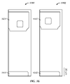
- FIG. 36 illustrates the patterning of a first metal layer (M 1 ) of pixels in the example IPS LCD display using LTPS in which a yVcom line is formed in an M 2 layer according to embodiments of the invention.
- FIG. 37 illustrates vias formed in pixels in the example IPS LCD display using LTPS in which a yVcom line is formed in an M 2 layer according to embodiments of the invention.
- FIG. 38 illustrates patterning of a second metal layer (M 2 ) of pixels in the example IPS LCD display using LTPS in which a yVcom line is formed in an M 2 layer according to embodiments of the invention.
- FIG. 39 illustrates a first layer of transparent conductive material, such as ITO, formed on pixels in the example IPS LCD display using LTPS in which a yVcom line is formed in an M 2 layer according to embodiments of the invention.
- transparent conductive material such as ITO
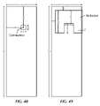
- FIG. 40 illustrates connections in the example IPS LCD display using LTPS in which a yVcom line is formed in an M 2 layer according to embodiments of the invention.
- FIG. 41 illustrates a second layer of transparent conductor, such as ITO, formed on pixels in the example IPS LCD display using LTPS in which a yVcom line is formed in an M 2 layer according to embodiments of the invention.
- FIG. 42 illustrates a plan view of completed pixels in the example IPS LCD display using LTPS in which a yVcom line is formed in an M 2 layer according to embodiments of the invention.
- FIG. 43 illustrates a side view of a pixel in the example IPS LCD display using LTPS in which a yVcom line is formed in an M 2 layer according to embodiments of the invention.
- FIG. 44 illustrates a semiconductor layer of poly-Si in an example ECB LCD display using LTPS according to embodiments of the invention.
- FIG. 45 illustrates a first layer of metal (M 1 ) in the example ECB LCD display using LTPS according to embodiments of the invention.
- FIG. 46 illustrates connections in the example ECB LCD display using LTPS according to embodiments of the invention.
- FIG. 47 illustrates a second metal layer (M 2 ) in the example ECB LCD display using LTPS according to embodiments of the invention.
- FIG. 48 illustrates a connection layer in the example ECB LCD display using LTPS according to embodiments of the invention.
- FIG. 49 illustrates a reflector layer in the example ECB LCD display using LTPS according to embodiments of the invention.
- FIG. 50 illustrates an ITO layer in the example ECB LCD display using LTPS according to embodiments of the invention.
- FIG. 51 illustrates a completed pixel in the example ECB LCD display using LTPS according to embodiments of the invention.
- FIG. 52 illustrates a side view of a pixel in the example ECB LCD display using LTPS according to embodiments of the invention.
- FIG. 53 illustrates a calculation of the storage capacitance of a pixel in the example ECB LCD display using LTPS according to embodiments of the invention.
- FIG. 54 illustrates an aperture ratio estimation of pixels in the example ECB LCD display using LTPS according to embodiments of the invention.
- FIG. 55 illustrates an example modification in the example ECB LCD display using LTPS according to embodiments of the invention.
- FIG. 56 illustrates a portion of a touch screen that includes an example grounded separator region according to embodiments of the invention.
- FIG. 57 is a side view of the example touch screen of FIG. 56 , which illustrates an example high R shield according to embodiments of the invention.
- FIG. 58 illustrates a side view of a portion of an example touch screen including black mask lines of a black mask and metal lines under the black mask lines according to embodiments of the invention.
- FIG. 59 illustrates an example black mask layout according to embodiments of the invention.
- FIG. 60 illustrates an example IPS-based touch-sensing display in which the pixel regions serve multiple functions.
- FIG. 61 illustrates an example computing system that can include one or more of the example embodiments of the invention.
- FIG. 62 a illustrates an example mobile telephone that can include a touch screen including pixels with dual-function capacitive elements according to embodiments of the invention.
- FIG. 62 b illustrates an example digital media player that can include a touch screen including pixels with dual-function capacitive elements according to embodiments of the invention.
- FIG. 62 c illustrates an example personal computer that can include a touch screen including pixels with dual-function capacitive elements according to embodiments of the invention.
- This relates to displays including pixels with dual-function capacitive elements.
- these dual-function capacitive elements form part of the display system that generates an image on the display, and also form part of a touch sensing system that senses touch events on or near the display.
- the capacitive elements can be, for example, capacitors in pixels of an LCD display that are configured to operate individually, each as a pixel storage capacitor, or electrode, of a pixel in the display system, and are also configured to operate collectively as elements of the touch sensing system.
- a display with integrated touch sensing capability may be manufactured using fewer parts and/or processing steps, and the display itself may be thinner and brighter.
- FIG. 1 is a partial circuit diagram of an example LCD display 100 including a plurality of LCD pixels according to embodiments of the present invention.
- the pixels of panel 100 are configured such that they are capable of dual-functionality as both LCD pixels and touch sensor elements. That is, the pixels include capacitive elements or electrodes, that can operate as part of the LCD display circuitry of the pixels and that can also operate as elements of touch sensing circuitry. In this way, panel 100 can operate as an LCD display with integrated touch sensing capability.
- FIG. 1 shows details of pixels 101 , 102 , 103 , and 104 of display 100 .
- Pixel 102 includes a thin film transistor (TFT) 155 with a gate 155 a , a source 155 b , and a drain 155 c .
- Pixel 102 also includes a storage capacitor, Cst 157 , with an upper electrode 157 a and a lower electrode 157 b , a liquid crystal capacitor, Clc 159 , with a pixel electrode 159 a and a common electrode 159 b , and a color filter voltage source, Vcf 161 .
- Vcf can be, for example, a fringe field electrode connected to a common voltage line in parallel with Cst 157 .
- Vcf 151 can be, for example, an ITO layer on the color filter glass.
- Pixel 102 also includes a portion 117 a of a data line for green (G) color data, Gdata line 117 , and a portion 113 b of a gate line 113 .
- Gate 155 a is connected to gate line portion 113 b
- source 155 b is connected to Gdata line portion 117 a .
- Upper electrode 157 a of Cst 157 is connected to drain 155 c of TFT 155
- lower electrode 157 b of Cst 157 is connected to a portion 121 b of a common voltage line that runs in the x-direction, xVcom 121 .
- Pixel electrode 159 a of Clc 159 is connected to drain 155 c of TFT 155
- common electrode 159 b of Clc 159 is connected to Vcf 151 .
- Pixel 103 The circuit diagram of pixel 103 is identical to that of pixel 102 . However, color data line 119 running through pixel 103 carries blue (B) color data. Pixels 102 and 103 can be, for example, conventional LCD pixels.
- pixel 101 includes a thin film transistor (TFT) 105 with a gate 105 a , a source 105 b , and a drain 105 c .
- Pixel 101 also includes a storage capacitor, Cst 107 , with an upper electrode 107 a and a lower electrode 107 b , a liquid crystal capacitor, Clc 109 , with a pixel electrode 109 a and a common electrode 109 b , and a color filter voltage source, Vcf 111 .
- Pixel 101 also includes a portion 115 a of a data line for red (R) color data, Rdata line 115 , and a portion 113 a of gate line 113 .
- R red
- Gate 105 a is connected to gate line portion 113 a , and source 105 b is connected to Rdata line portion 115 a .
- Upper electrode 107 a of Cst 107 is connected to drain 105 c of TFT 105
- lower electrode 107 b of Cst 107 is connected to a portion 121 a of xVcom 121 .
- Pixel electrode 109 a of Clc 109 is connected to drain 105 c of TFT 105
- common electrode 109 b of Clc 109 is connected to Vcf 111 .
- pixel 101 also includes a portion 123 a of a common voltage line running in the y-direction, yVcom 123 .
- pixel 101 includes a connection 127 that connects portion 121 a to portion 123 a .
- connection 127 connects xVcom 121 and yVcom 123 .
- Pixel 104 is similar to pixel 101 , except that a portion 125 a of a yVcom 125 has a break (open) 131 , and a portion 121 b of xVcom 121 has a break 133 .
- the lower electrodes of storage capacitors of pixels 101 , 102 , and 103 are connected together by xVcom 121 .
- This is a conventional type of connection in many LCD panels and, when used in conjunction with conventional gate lines, data lines, and transistors, allows pixels to be addressed.
- the addition of vertical common voltage lines along with connections to the horizontal common voltage lines allows grouping of pixels in both the x-direction and y-direction, as described in further detail below.
- yVcom 123 and connection 127 to xVcom 121 can allow the storage capacitors of pixels 101 , 102 , and 103 to be connected to storage capacitors of pixels that are above and below pixels 101 , 102 , 103 (the pixels above and below are not shown).
- the pixels immediately above pixels 101 , 102 , and 103 can have the same configurations as pixels 101 , 102 , and 103 , respectively.
- the storage capacitors of the pixels immediately above pixels 101 , 102 , and 103 would be connected to the storage capacitors of pixels 101 , 102 , and 103 .
- an LCD panel could be configured such that the storage capacitors of all pixels in the panel are connected together, for example, through at least one vertical common voltage line with connections to a plurality of horizontal common voltage lines.
- Another LCD panel could be configured such that different groups of pixels are connected together to form a plurality of separate regions of connected-together storage capacitors.
- yVcom 125 of panel 100 has a break 131 , which can allow pixels above the break to be isolated from pixels below the break.
- xVcom 121 has a break 133 , which can allow pixels to the right of the break to be isolated from pixels to the left of the break.
- FIGS. 2A and 2B illustrate example regions formed by breaks in vertical and horizontal common voltage lines according to embodiments of the invention.
- FIG. 2A shows a TFT glass region layout.
- FIG. 2A shows a region 201 , a region 205 , and a region 207 .
- Each region 201 , 205 , and 207 is formed by linking storage capacitors of a plurality of pixels (not shown in detail) through common voltage lines in the vertical direction (y-direction) and in the horizontal direction (x-direction).
- the enlarged area of FIG. 2A shows pixel blocks 203 a - e .
- a pixel block includes one or more pixels, in which at least one of the pixels includes a vertical common line, yVcom.
- FIG. 1 shows a TFT glass region layout.
- FIG. 2A shows a region 201 , a region 205 , and a region 207 .
- Each region 201 , 205 , and 207 is formed by linking storage capacitor
- FIG. 1 illustrates a pixel block that includes pixels 101 - 103 , in which pixel 101 includes yVcom 123 .
- pixel block 203 a is connected in the horizontal direction to pixel block 203 b through a horizontal common line, xVcom 206 .
- pixel block 203 a is connected in the vertical direction to pixel block 203 c through a vertical common line, yVcom 204 .
- a break in xVcom 206 prevents block 203 a from being connected to block 203 d
- a break in yVcom 204 prevents block 203 a from being connected to block 203 e .
- Regions 201 and 207 form a capacitive element that can provide touch sensing information when connected to suitable touch circuitry, such as touch circuitry 213 of touch ASIC 215 .
- suitable touch circuitry such as touch circuitry 213 of touch ASIC 215 .
- the connection is established by connecting the regions to switch circuitry 217 , which is described in more detail below.
- switch circuitry 217 which is described in more detail below.
- the XVCOM and YVCOM regions may simply extended with metal traces that go to the Touch ASIC which is bonded to the glass in a similar way as the LCD driver chip (through anisotropic conductive adhesive).
- region 201 and region 205 form a capacitive element that can provide touch information when connected to touch circuitry 213 .
- region 201 serves as a common electrode to regions 205 and 207 , which are called, for example, sense electrodes.
- regions 205 and 207 which are called, for example, sense electrodes.
- the regions connected-together storage capacitors of pixels can be formed using vias between common voltage lines, such as xVcom and yVcom in FIG. 1 , and using selective breaks in the common voltage lines.
- FIG. 2A illustrates one way in which vias or other connections and selective breaks can be used to create capacitive regions that can span many pixels.
- regions of other shapes and configurations can be created.
- FIG. 2B shows a CF glass patterned ITO region layout, which may or may not be needed, depending on the type of LCD technology used by the pixel. For example, such CF ITO regions would not be needed in the case that the LCD pixel utilizes in-plane-switching (IPS).
- FIG. 2B is directed to non-IPS LCD displays in which a voltage is applied to liquid crystal between an upper and lower electrode.
- FIG. 2B shows upper regions 221 , 223 , and 225 , which correspond to lower (in non-IPS displays) regions 201 , 205 , and 207 , respectively, of FIG. 2A .
- FIG. 2B shows conductive dots 250 contacting regions 251 , 255 , and 257 .
- Conductive dots 250 connect the corresponding upper and lower regions such that when to the upper electrodes of pixels in an upper region are driven, the corresponding lower electrodes of pixels in the lower region are also driven.
- the relative voltage between the upper and lower electrodes remains constant, even while the pixels are being driven by, for example, a modulated signal.
- the voltage applied to the liquid crystal can remain constant during a touch phase, for example.
- the constant relative voltage can be the pixel voltage for operation of the LCD pixel. Therefore, the pixels can continue to operate (i.e., display an image) while touch input is being detected.
- a touch sensing operation will be described with reference to FIGS. 3-5B .
- the operation is described in terms of a single drive pixel and a single sense pixel.
- the drive pixel is connected to other drive pixels in a drive region and the sense pixel is connected to other sense pixels in the sense region, as described above.
- the entire drive region is driven, and the entire sense region can contribute to the sensing of touch.
- FIG. 3 shows partial circuit diagrams of a pixel 301 of a drive region and a pixel 303 of an example sense region.
- Pixels 301 and 303 include TFTs 307 and 309 , gate lines 311 and 312 , data lines 313 and 314 , xVcom lines 315 and 316 , fringe field electrodes 319 and 321 , and storage capacitors 323 and 325 .
- Storage capacitors 323 and 325 each have a capacitance of about 300 fF (femto-Farads).
- a lower electrode of fringe field electrode 321 of pixel 303 can be connected, through xVcom 316 , to a charge amplifier 326 in the sense circuitry.
- Charge amplifier 326 holds this line at a virtual ground such that any charge that gets injected from fringe field electrode 321 shows up as a voltage output of the amplifier.
- the feedback element of the amplifier is shown as a capacitor, it may also function as a resistor or a combination of a resistor and capacitor.
- the feedback can also be, for example, a resistor and capacitor feedback for minimizing die-size of the touch sensing circuitry.
- FIG. 3 also shows a finger 327 that creates a stray capacitance of approximately 3 fF with a cover glass (not shown), and shows other stray capacitances in the pixels, each of which is approximately 3 fF.
- FIG. 4A shows example signals applied through xVcom 315 to the pixels of the drive region, including pixel 301 , during an LCD phase and during a touch phase.
- xVcom 315 is driven with a square wave signal of 2.5V+/ ⁇ 2.5V, in order to perform LCD inversion.
- the LCD phase is 12 ms in duration.
- xVcom 315 is driven with 15 to 20 consecutive stimulation phases lasting 200 microseconds each.
- the stimulation signals in this case are sinusoidal signals of 2.5V+/ ⁇ 2V each having the same frequency and a relative phase of either 0 degrees or 180 degrees (corresponding to “+” and “ ⁇ ” in FIG. 4A ).
- the touch phase is 4 ms in duration.
- FIG. 5A shows details of the operation of storage capacitor 323 during the touch phase.
- the capacitance of storage capacitor 323 is much higher than the other capacitances, i.e., stray capacitances shown in FIG. 3 .
- almost all (approximately 90%) of the AC component of the 2.5V+/ ⁇ 2V sinusoidal stimulation signal that is applied at the lower electrode of the storage capacitor is transferred to the upper electrode. Therefore, the upper electrode, which is charged to 4.5 volts DC for the operation of the LCD, sees a sinusoidal signal of 4.5V+/ ⁇ 1.9V.
- These signals are passed to the corresponding left and right comb structures of fringe field electrode 319 .
- fringe field electrode 319 can be modulated with a signal having an AC component of approximately +/ ⁇ 2V in amplitude (+/ ⁇ 2V on one, +/ ⁇ 1.9V on the other).
- fringe field electrode 319 together with the other fringe field electrodes of pixels in the drive region being similarly driven, can operate as a drive line for capacitive sensing.
- fringe field electrode 319 is configured to operate as a drive element for the touch sensing system, the fringe field electrode continues to operate as a part of the LCD display system.
- the voltages of the comb structures of fringe field electrode are each modulated at approximately +/ ⁇ 2V, the relative voltage between the comb structures remains approximately constant at 2V+/ ⁇ 0.1V.
- This relative voltage is the voltage that is seen by the liquid crystal of the pixel for the LCD operation.
- the 0.1V AC variance in the relative voltage during the touch phase should have an acceptably low affect on the LCD display, particularly since the AC variance would typically have a frequency that is higher than the response time for the liquid crystal.
- the stimulation signal frequency and hence the frequency of the AC variance, would typically be more than 100 kHz.
- the response time for liquid crystal is typically less than 100 Hz. Therefore, the fringe field electrode's function as a drive element in the touch system should not interfere with the fringe field electrode's LCD function.
- FIG. 4B shows signals applied through xVcom 316 to the pixels of the sense region, including pixel 303 , during the LCD and touch phases described above.
- xVcom 316 is driven with a square wave signal of 2.5V+/ ⁇ 2.5V in order to perform LCD inversion during the LCD phase.
- xVcom 316 is connected to amplifier 326 , which holds the voltage at or near a virtual ground of 2.5V. Consequently, fringe field electrode 321 is also held at 2.5V.
- fringing electrical fields propagate from fringe field electrode 319 to fringe field electrode 321 .
- the fringing electric fields are modulated at approximately +/ ⁇ 2V by the drive region.
- these fields are received by the top electrode of fringing field electrode 321 , most of the signal gets transferred to the lower electrode, because pixel 303 has the same or similar stray capacitances and storage capacitance as pixel 301 .
- xVcom 316 is connected to charge amplifier 326 , and is being held at virtual ground, any charge that gets injected will show up as an output voltage of the charge amplifier. This output voltage provides the touch sense information for the touch sensing system. For example, when finger 327 gets close to the fringing fields, it captures some fields and grounds them, which causes a disturbance in the fields.
- This disturbance can be detected by the touch system as a disturbance in the output voltage of charge amplifier 326 .
- FIG. 5B shows that approximately 90% of a received fringing field at pixel 302 which impinges onto the electrode half of the capacitor which is also connected to the drain of the TFT 325 will be transferred to charge amplifier 326 . 100% of the charge that impinges onto the electrode half of the capacitor which is connected directly to XVCOM 316 will be transferred to charge amplifier 326 .
- the ratio of charge impinging onto each electrode will depend on the LCD design. For non-IPS, near 100% of the finger affected charge will impinge on the VCOM electrode because the patterned CF plate is nearest the finger.
- the ratio will be closer to half and half because each part of the electrode has approximately equal area (or 1 ⁇ 4 vs. 3 ⁇ 4) facing the finger.
- the fringing electrodes are not coplanar, and the majority of the upward facing area is devoted to the VCOM electrode.
- FIGS. 3 , 4 A-B, and 5 A-B are described using single pixels for the sake of clarity.
- Some example layouts and operations of drive regions and sense regions according to embodiments of the invention will now be described with reference to FIGS. 6A-C , 7 , 8 A-C, 9 A-C, and 10 .
- FIG. 6A illustrates a partial view of an example touch screen 600 having regions of pixels with dual-function capacitive elements that operate as LCD elements and as touch sensors according to embodiments of the invention.
- touch screen 600 having eight columns (labeled a through h) and six rows (labeled 1 through 6 ) is shown, although it should be understood that any number of columns and rows can be employed.
- Columns a through h can be formed from column-shaped regions, although in the example of FIG. 6A , one side of each column includes staggered edges and notches designed to create separate sections in each column.
- Each of rows 1 through 6 can be formed from a plurality of distinct patches or pads within the regions, each patch connected to a border area through one or more yVcom lines running to the border area of touch screen 600 for enabling all patches in a particular row to be connected together through metal traces (not shown in FIG. 6A ) running in the border areas. These metal traces can be routed to a small area on one side of touch screen 600 and connected to a flex circuit 602 .
- the patches forming the rows can be formed, by selective placement of breaks in xVcom lines and yVcom lines, for example, in a generally pyramid-shaped configuration. In FIG. 6A , for example, the patches for rows 1 - 3 between columns a and b are arranged in an inverted pyramid configuration, while the patches for rows 4 - 6 between columns a and b are arranged in an upright pyramid configuration.
- FIG. 6B illustrates a partial view of example touch screen 600 including metal traces 604 and 606 running in the border areas of the touch screen according to embodiments of the invention. Note that the border areas in FIG. 6B are enlarged for clarity.
- Each column a-h can include extended yVcom line(s) 608 that allows the column to be connected to a metal trace through a via (not shown in FIG. 6B ).
- One side of each column includes staggered edges 614 and notches 616 designed to create separate sections in each column.
- Each row patch 1 - 6 can include extended yVcom line(s) 610 that allows the patch to be connected to a metal trace through a via (not shown in FIG. 6B ).
- yVcom lines 610 can allow each patch in a particular row to be self-connected to each other. Because all metal traces 604 and 606 are formed on the same layer, they can all be routed to the same flex circuit 602 .
- touch screen 600 is operated as a mutual capacitance touch screen, either the columns a-h or the rows 1 - 6 can be driven with one or more stimulation signals, and fringing electric field lines can form between adjacent column areas and row patches.
- FIG. 6B it should be understood that although only electric field lines 612 between column a and row patch 1 (a- 1 ) are shown for purposes of illustration, electric field lines can be formed between other adjacent column and row patches (e.g. a- 2 , b- 4 , g- 5 , etc.) depending on what columns or rows are being stimulated.
- each column-row patch pair e.g.
- a- 1 , a- 2 , b- 4 , g- 5 , etc. can represent a two-region touch pixel or sensor at which charge can be coupled onto the sense region from the drive region.
- some of the fringing electric field lines that extend beyond the cover of the touch screen are blocked by the finger, reducing the amount of charge coupled onto the sense region. This reduction in the amount of coupled charge can be detected as part of determining a resultant “image” of touch.
- no separate reference ground is needed, so no second layer on the back side of the substrate, or on a separate substrate, is needed.
- Touch screen 600 can also be operated as a self-capacitance touch screen.
- a reference ground plane can be formed on the back side of the substrate, on the same side as the patches and columns but separated from the patches and columns by a dielectric, or on a separate substrate.
- each touch pixel or sensor has a self-capacitance to the reference ground that can be changed due to the presence of a finger.
- the self-capacitance of columns a-h can be sensed independently, and the self-capacitance of rows 1 - 6 can also be sensed independently.
- FIG. 6C illustrates an example connection of columns and row patches to the metal traces in the border area of the touch screen according to embodiments of the invention.
- FIG. 6C represents “Detail A” as shown in FIG. 6B , and shows column “a” and row patches 4 - 6 connected to metal traces 618 through yVcom lines 608 and 610 . Because yVcom lines 608 and 610 are separated from metal traces 618 by a dielectric material, vias 620 formed in the dielectric material allow the yVcom lines to connect to the metal traces.
- the metal traces 618 can be formed in the same layer as the yVcom lines.
- the touch traces can be routed in the same M 1 and M 2 layers that are conventional in LCD'S, also sometimes referred to as “gate metal” and “source/drain metal”.
- the dielectric insulation layer can be referred to as a “inner layer dielectric” or “ILD”.
- column edges 614 and row patches 4 - 6 can be staggered in the x-dimension because space should be made for the touch pixels containing yVcom lines 610 connecting row patches 4 and 5 . (It should be understood that row patch 4 in the example of FIG. 6C is really two patches stuck together.)
- row patch 4 in the example of FIG. 6C is really two patches stuck together.
- row patch 6 can be slimmer than row patch 5 or 6 , and an imbalance would be created between the regions of touch pixel a- 6 .
- FIG. 7 illustrates a top view of an example column and adjacent row patches according to embodiments of the invention. It can be generally desirable to make the mutual capacitance characteristics of touch pixels a- 4 , a- 5 and a- 6 relatively constant to produce a relatively uniform z-direction touch sensitivity that stays within the range of touch sensing circuitry. Accordingly, the column areas a 4 , a 5 and a 6 should be about the same as row patch areas 4 , 5 and 6 . To accomplish this, column section a 4 and a 5 , and row patch 4 and 5 can be shrunk in the y-direction as compared to column section a 6 and row patch 6 so that the area of column segment a 4 matches the area of column segments a 5 and a 6 . In other words, touch pixel a 4 - 4 will be wider but shorter than touch pixel a 6 - 6 , which will be narrower but taller.
- the touch pixels or sensors can be slightly skewed or misaligned in the x-direction
- the x-coordinate of a maximized touch event on touch pixel a- 6 e.g. a finger placed down directly over touch pixel a- 6
- this misalignment can be de-warped in a software algorithm to re-map the touch pixels and remove the distortion.
- a typical touch panel grid dimension can have touch pixels arranged on 5.0 mm centers
- a more spread-out grid having about 6.0 mm centers can be desirable to reduce the overall number of electrical connections in the touch screen.
- spreading out the sensor pattern can cause erroneous touch readings.
- FIG. 8A is an example plot of an x-coordinate of a finger touch versus mutual capacitance seen at a touch pixel for a two adjacent touch pixels a- 5 and b- 5 in a single row having wide spacings.
- plot 800 represents the mutual capacitance seen at touch pixel a- 5 as the finger touch moves continuously from left to right
- plot 802 represents the mutual capacitance seen at touch pixel b- 5 as the finger touch moves continuously from left to right.
- FIG. 8A illustrates that even though the finger is never lifted from the surface of the touch screen, it can erroneously appear at 810 that the finger has momentarily lifted off the surface. This location 810 can represent a point about halfway between the two spread-out touch pixels.
- FIG. 8B is an example plot of an x-coordinate of a finger touch versus mutual capacitance seen at a touch pixel for a two adjacent touch pixels a- 5 and b- 5 in a single row having wide spacings where spatial interpolation has been provided according to embodiments of the invention.
- a drop in the mutual capacitance 804 is seen at touch pixel a- 5 when the finger touch passes directly over touch pixel a- 5
- a similar drop in the mutual capacitance 806 is seen at touch pixel b- 5 when the finger touch passes directly over touch pixel b- 5 . Note, however, that the rise and fall in the mutual capacitance value occurs more gradually than in FIG. 8A .
- FIG. 8B illustrates that as the finger moves from left to right over touch pixel a- 5 and b- 5 , a touch event is always detected at either touch pixel a- 5 or b- 5 . In other words, this “blurring” of touch events is helpful to prevent the appearance of false no-touch readings.
- the thickness of the coverglass for the touch screen can be increased to create part or all of the spatial blurring or filtering shown in FIG. 8B .
- FIG. 8C illustrates a top view of an example column and adjacent row patch pattern useful for larger touch pixel spacings according to embodiments of the invention.
- FIG. 8C illustrates an example embodiment in which sawtooth region edges 812 are employed within a touch pixel elongated in the x-direction.
- the sawtooth region edges can allow fringing electric field lines 814 to be present over a larger area in the x-direction so that a touch event can be detected by the same touch pixel over a larger distance in the x-direction.
- the sawtooth configuration of FIG. 8C is only an example, and that other configurations such serpentine edges and the like can also be used. These configurations can further soften the touch patterns and create additional spatial filtering and interpolation between adjacent touch pixels as shown in FIG. 8B .
- FIG. 9A illustrates example touch screen 900 including sense (or drive) regions (C 0 -C 5 ) formed as columns 906 and rows of polygonal regions (bricks) 902 , where each row of bricks forms a separate drive (or sense) region (R 0 -R 7 ) according to embodiments of the invention.
- connecting yVcom lines 904 are routed along only one side of the bricks (a so-called “single escape” configuration).
- a touch screen 900 having six columns and eight rows is shown, it should be understood that any number of columns and rows can be employed.
- connecting yVcom lines 904 can be routed from the bricks along one side of the bricks in a single escape configuration to a particular bus line 910 .
- Ground isolation regions 908 can be formed between connecting yVcom lines 904 and adjacent columns 906 to reduce the capacitive coupling between the connecting yVcom lines and the columns. Connections for each bus line 910 and for columns 906 can be brought off touch screen 900 through flex circuit 912 .
- FIG. 9B illustrates a close-up view of a portion of the example touch screen 900 of FIG. 9A , showing how bricks 902 can be routed to bus lines 910 using connecting yVcom lines 904 in a single escape configuration according to embodiments of the invention.
- the longer connections, more yVcom lines 904 e.g. trace R 7
- the shorter connecting yVcom lines e.g. trace R 2
- FIG. 9C illustrates a portion of example touch screen 900 of FIG. 9A including bricks 902 associated with columns C 0 and C 1 and connecting yVcom lines 904 (illustrated symbolically as thin lines) coupling the bricks to bus lines 910 according to embodiments of the invention.
- bus line B 0 is coupled to brick R 0 C 0 (the closest brick to B 0 adjacent to column C 0 ) and R 0 C 1 (the closest brick to B 0 adjacent to column C 1 ).
- Bus line B 1 is coupled to brick R 1 C 0 (the next closest brick to B 0 adjacent to column C 0 ) and R who 1 (the next closest brick to B 0 adjacent to column C 1 ).
- the pattern repeats for the other bus lines such that bus line B 7 is coupled to brick R 7 C 0 (the farthest brick from B 0 adjacent to column C 0 ) and R 7 C 1 (the farthest brick from B 0 adjacent to column C 1 ).
- FIG. 10 illustrates a portion of example zig-zag double interpolated touch screen 1000 that can further reduce the stray capacitance between the connecting yVcom lines and the sense regions according to embodiments of the invention.
- polygonal regions 1002 representing the drive (or sense) regions are generally pentagonal in shape and staggered in orientation, with some of the polygonal areas near the end of the panel being cut-off pentagons.
- Sense (or drive) regions 1004 are zig-zag shaped, with ground guards 1006 between the sense (or drive) regions and pentagons 1002 . All connecting yVcom lines 1008 are routed in channels 1010 between pentagons 1002 .
- each touch pixel or sensor is characterized by electric field lines 1016 formed between a pentagon and an adjacent sense (or drive) region 1004 .
- connecting yVcom lines 1008 do not run alongside any sense (or drive) regions 1004 , but instead run between pentagons 1002 .
- the stray capacitance between connecting yVcom lines 1008 and sense (or drive) regions 1004 is minimized, and spatial cross-coupling is also minimized.
- the distance between connecting yVcom lines 1008 and sense (or drive) regions 1004 was only the width of ground guard 1006 , but in the embodiment of FIG. 10 , the distance is the width of the ground guard plus the width of pentagon 1002 (which varies along the length of its shape).
- the pentagons for row R 14 at an end of the touch screen can be truncated. Accordingly, the calculated centroids of touch 1012 for R 14 can be offset in the y-direction from their true position. In addition, the calculated centroids of touch for any two adjacent rows will be staggered (offset from each other) in the x-direction by an offset distance. However, this misalignment can be de-warped in a software algorithm to re-map the touch pixels and remove the distortion.
- a reference ground plane can be formed either on the back side of the substrate, or on the same side of the substrate as the polygonal regions and sense regions but separated from the polygonal regions and sense regions by a dielectric, or on a separate substrate.
- each touch pixel or sensor has a self-capacitance to the reference ground that can be changed due to the presence of a finger.
- a touch screen can use both mutual and self-capacitance measurements in a time-multiplexing fashion to gather additional information and each measurement type can compensate the weaknesses of the other.
- FIGS. 11-24 are directed to an example electrically controlled birefringence (ECB) LCD display using amorphous silicon (a-Si).
- FIGS. 25-34 are directed to an example IPS LCD display using low temperature polycrystalline silicon (LTPS).
- FIGS. 35-43 are directed to another example IPS LCD display using LTPS.
- FIGS. 44-55 are directed to an example ECB LCD display using LTPS.
- FIGS. 11-18 An example process of manufacturing an ECB LCD display according to embodiments of the invention will now be described with reference to FIGS. 11-18 .
- the figures show various stages of processing of two pixels, a pixel 1101 and a pixel 1102 , during the manufacture of the ECB LCD display.
- the resulting pixels 1101 and 1102 form electrical circuits equivalent to pixels 101 and 102 , respectively, of FIG. 1 .
- FIG. 11 shows the patterning of a first metal layer (M 1 ) of pixels 1101 and 1102 .
- the M 1 layer for pixel 1102 includes a gate 1155 a , a portion 1113 b of a gate line 1113 , a lower electrode 1157 b of a storage capacitor (not shown except for lower electrode 1157 b ), and a portion 1121 b of an xVcom 1121 .
- Pixel 1101 includes a gate 1105 a , a lower electrode 1107 b of a storage capacitor (not shown except for lower electrode 1107 b ), a portion 1113 a of gate line 1113 , and a portion 1121 a of xVcom 1121 .
- Pixel 1101 also includes a portion 1123 a of a yVcom 1123 (shown as dotted lines), which includes an additional portion 1140 .
- Portion 1123 a has a connection point 1141 and a connection point 1143 .
- a gate line 1113 and an xVcom 1121 run through both pixels 1101 and 1102 in an x-direction.
- Gate line 1113 connects to gates 1105 a and 1155 a
- xVcom 1121 connects lower electrode 1107 b and 1157 b .
- Portion 1123 a of yVcom 1123 connects to xVcom 1121 in pixel 1101 .
- FIG. 12 shows a subsequent patterning step in the process of manufacturing pixels 1101 and 1102 , in which island patterns of poly-Si are formed.
- the island patterns for the pixels are similar, except that semiconductor portion 1201 and 1203 of pixel 1102 are slightly different that semiconductor portions 1205 and 1207 of pixel 1101 .
- portion 1205 is slightly smaller than portion 1201 . This is due, in part, to allow xVcom 1121 to be connected in the vertical direction (y-direction) with other xVcom lines through yVcom 1123 , as is described in greater detail below.
- FIG. 13 shows connections 1301 and 1302 formed in pixel 1101 . Pixel 1102 does not include such connections. The operation of connections 1301 and 1302 is described in more detail below with reference to FIG. 14 .
- FIG. 14 shows patterning of a second metal layer (M 2 ) of pixels 1101 and 1102 .
- the M 2 layer of pixel 1102 forms a portion 1417 a of a green color data line, Gdata 1417 (shown as a dotted line in FIG. 14 ), a source 1455 b , a drain 1455 c , and an upper electrode 1457 a .
- the M 2 layer of pixel 1101 forms a portion 1415 a of a red color data line, Rdata 1415 (shown as a dotted line in FIG. 14 ), a source 1405 b , a drain 1405 c , and upper electrode 1407 a .
- the M 2 layer of pixel 1101 also forms portions 1423 a and 1423 b of yVcom 1123 (shown a dotted line in FIG. 14 ).
- Upper electrode 1407 a is smaller than upper electrode 1457 a , which allows portion 1423 a to be formed in the M 2 layer of the pixel 1101 .
- Portion 1423 a has a connection point 1441
- portion 1423 b has a connection point 1443 .
- FIGS. 11 , 13 and 14 together illustrate that pixel 1101 includes a vertical common line (yVcom 1415 ) that allows connection of xVcom 1121 with other xVcom lines in the vertical direction (y-direction).
- yVcom 1415 a vertical common line
- the figures show portion 1423 a is connected to portion 1123 a through connection 1301 at connection points 1441 and 1141 , respectively.
- Portion 1123 a is connected to 1423 b through connection 1302 at points 1143 and 1443 , respectively.
- the figures show a continuous portion of yVcom 1123 is formed in pixel 1101 by the connection of multiple structures of the pixel.
- yVcom portion 1123 a is connected to xVcom portion 1121 a . Consequently, the structure of pixel 1101 shown in the figures allows connection in the vertical direction of multiple xVcom lines.
- FIG. 15 shows planarization (PLN) contact layers 1501 and 1503 of pixels 1101 and 1102 , respectively.
- FIG. 16 shows reflector (REF) layers 1601 and 1603 of pixels 1101 and 1102 , respectively.
- FIG. 17 shows passivation (PASS) contacts 1701 and 1703 of pixels 1101 and 1102 , respectively.
- FIG. 18 shows semi-transparent conductive material, such as IPO, layers that form pixel electrodes 1801 and 1803 of pixels 1101 and 1102 , respectively.
- FIG. 19 shows a plan view of completed pixels 1101 and 1102 .
- FIGS. 20A-B illustrate side views of completed pixel 1101 take along the paths shown in the top views shown in the figures.
- FIGS. 20C-D illustrate side views of pixels 1102 and 1101 along the lines shown in FIG. 19 .
- FIG. 20A shows a side view of pixel 1101 .
- the portion of the M 1 layer shown in FIG. 20A includes gate line portion 1113 b , gate 1155 a , lower electrode 1157 b , and xVcom portion 1121 b .
- the poly-Si layer shown in FIG. 20A includes poly-Si 1205 and poly-Si 1201 .
- the M 2 layer shown in FIG. 20A includes source 1455 b , drain 1465 c , and upper electrode 1457 a .
- FIG. 20A also shows planarization layer 1503 , reflector layer 1603 , passivation contact 1703 , and transparent conductor layer 1103 .
- FIG. 20B shows another side view of pixel 1101 .
- the M 1 layer shown in FIG. 20B includes gate line portion 1113 a , gate 1105 a , lower electrode 1107 b , and xVcom portion 1121 a .
- FIG. 20B also shows an adjacent pixel 2001 , which has the same structure as pixel 1101 .
- the poly-Si layer shown in FIG. 20B includes poly-Si portion 1211 and poly-Si portion 1207 .
- the M 2 layer shown in FIG. 20B includes source 1405 b , drain 1405 c , and upper electrode 1407 a.
- FIG. 20C shows a side view of pixel 1102 along the line shown in FIG. 19 .
- the M 1 layer shown in FIG. 20C includes gate line portion 1113 b , gate 1155 a , and xVcom portion 1121 b .
- FIG. 20C also shows a gate insulator 2003 deposited on top of M 1 .
- Poly-Si portion 1203 and an additional poly-Si portion are also shown in FIG. 20C .
- FIG. 20D shows a side view of pixel 1101 along the line shown in FIG. 19 .
- the M 1 layer shown in FIG. 20D includes gate line portion 1113 a , gate 1105 a , and yVcom portion 1123 a , which includes an intersection with xVcom portion 1121 a .
- Connections 1301 and 1302 contact connection points 1141 and 1143 , respectively, of yVcom portion 1123 a .
- FIG. 20D also shows a gate insulator layer 2005 and poly-Si portion 1209 .
- FIG. 20D includes yVcom portion 1423 a , which connects with connection 1301 at connection point 1441 , and yVcom portion 1423 b , which connects with connection 1302 at connection point 1443 .
- the vertical common line, yVcom 1123 (shown in FIG. 20D as dashed lines) runs through pixel 1181 as yVcom portion 1423 a , connection 1301 , yVcom portion 1123 a , connection 1302 , and yVcom portion 1423 b .
- FIG. 20D also shows a portion of an adjacent pixel that includes structure identical to pixel 1101 .
- the adjacent pixel includes a yVcom portion that is connected, via a connection, to an xVcom portion.
- FIG. 20D illustrates that a xVcom portion 1121 a can be connected to an adjacent pixels xVcom portion with a yVcom line.
- FIGS. 21 and 22 show a comparative analysis of the storage capacitance of pixels 1101 and 1102 .
- FIG. 21 shows the overlapping areas of the first and second metal layers that result in the capacitance C M1/M2 .
- C M1/M2 of pixel 1102 results from an overlap of approximately 360 square micrometers of the first and second metallic layers.
- the highlighted portions of pixel 1102 show the overlapping regions of the first metallic layer and the transparent conductor layer that result in C M1/ITO. As shown in FIG. 22 , the total overlap is approximately 360 square micrometers.
- C store C M1/M2 +C M1/ITO +C M2/ITO (2)
- FIGS. 21 and 22 show the areas of overlapping metal in pixel 1101 that result in the terms of equation 2 .
- FIG. 21 shows an overlapping region of the first and second metallic layers in pixel 1101 that equals approximately 503 square micrometers.
- FIG. 22 shows overlapping regions of the first metallic layer and the transparent conductor layer in pixel 1101 that equals approximately 360 square micrometers.
- FIG. 22 also shows an overlapping region of the second metallic layer and the transparent conductor layer that equals approximately 81 square micrometers.
- pixel 1101 has an extra area overlap that pixel 1102 does not.
- the overlap of the second metallic layer and the transparent conductor layer in pixel 1101 contributes an additional 81 square micrometers, which in turn contributes an additional amount of capacitance to the storage capacitance of pixel 1101 .
- FIG. 23 illustrates aperture ratio estimations for pixels 1101 and 1102 .
- Pixel 1101 has an aperture ratio of 41.4%.
- Pixel 1102 has an aperture ratio of 44.4%.
- FIG. 24 illustrates an example modification according to embodiments of the invention.
- the aperture ratios of the different pixels in a system may be made more similar, which may improve the appearance of the display.
- pixels 2401 and 2405 do not include connection portions in the y-direction.
- Pixel 2403 does include a connection portion in the y-direction, similar to pixel 1101 .
- FIGS. 25-34 are directed to an example IPS LCD display using low temperature polycrystalline silicon (LTPS).
- LTPS low temperature polycrystalline silicon
- FIGS. 25-31 An example process of manufacturing an IPS LCD display using LTPS according to embodiments of the invention will now be described with reference to FIGS. 25-31 .
- the figures show various stages of processing of two pixels, a pixel 2501 and a pixel 2502 , during the manufacture of the IPS LCD display using LTPS.
- the resulting pixels 2501 and 2502 form electrical circuits equivalent to pixels 101 and 102 , respectively, of FIG. 1 .
- FIGS. 25-30 Because the stages of processing shown in FIGS. 25-30 are the same for pixel 2501 and pixel 2502 , only one pixel is shown in each of these figures. However, it is understood that the stages of processing show in FIGS. 25-30 apply to both pixel 2501 and pixel 2502 .
- FIG. 25 shows the patterning of a layer of poly-Si of pixels 2501 and 2502 .
- Semiconductor portions 2505 , 2507 , and 2509 form the active region of a TFT, and serve as source, gate, and drain, respectively.
- FIG. 26 shows a subsequent patterning step in the process of manufacturing pixels 2501 and 2502 , in which a first metal layer (M 1 ) of pixels 2501 and 2502 is formed.
- the M 1 layer for the pixels 2501 / 2502 includes a gate 2605 a , a portion 2613 a of a gate line 2613 (shown as dotted lines), and a portion 2621 a of xVcom 2621 .
- Portion 2621 a includes a connection point 2623 .
- Gate line 2613 and xVcom 2621 run through pixels that are adjacent in the x-direction.
- FIG. 27 shows vias 2701 , 2703 , and 2705 formed in pixels 2501 / 2502 for connections to portion 2505 , portion 2509 , and connection point 2623 , respectively.
- FIG. 28 shows patterning of a second metal layer (M 2 ) of pixels 2501 / 2502 .
- the M 2 layer of the pixels forms a portion 2817 a of a color data line 2817 (shown as a dotted line in FIG. 28 ), which could carry red, green, or blue color data, for example.
- Portion 2817 a includes a connection 2819 that connects to portion 2505 through via 2701 .
- the M 2 layer also forms a connection 2821 with portion 2509 through via 2703 , and forms a connection 2823 to connection point 2623 through via 2705 .
- FIG. 29 shows a first layer of transparent conductive material, such as ITO, formed on pixels 2501 / 2502 .
- the first transparent conductor layer includes a pixel electrode 2901 .
- FIG. 29 also shows a portion 2905 of a pixel electrode of a pixel adjacent in the x-direction, and a portion 2907 of a pixel electrode of a pixel adjacent in the y-direction.
- FIG. 29 also shows a connection 2903 , which forms a connection between a common ITO layer described below and xVcom 2621 through connection point 2623 and a connection 3001 shown in FIG. 30 .
- FIG. 31 shows a second layer of transparent conductor, such as ITO, formed on pixel 2501 and pixel 2502 .
- the second layer on pixel 2502 forms a common electrode 3151 , which includes a connection point 3153 that connects to xVcom 2621 through connections 3001 and 2903 , and connection point 2623 .
- FIG. 31 also shows a portion 3155 of a common electrode of a pixel adjacent in the y-direction.
- pixel 2501 includes a common electrode 3101 formed of the second layer of transparent conductor.
- common electrode 3101 includes a connection point 3103 that connects to xVcom 2621 through connections 3001 and 2903 , and connection point 2623 .
- pixel 2501 also includes a connection 3107 between common electrode 3101 and a common electrode 3105 of a pixel adjacent in the y-direction.
- the common electrodes of pixels can be connected in the y-direction to form a yVcom line 3109 .
- common electrode 3101 is connected to xVcom 2621 and xVcom 2621 is connected to common electrodes of other pixels in the x-direction, the common electrodes of a region of pixels can be connected together to form a touch sensing element. Similar to the previous example embodiment, breaks in xVcom lines and yVcom lines can create separate regions of linked-together common electrodes that can be formed as an array of touch sensors.
- FIG. 32 shows a plan view of completed pixels 2501 and 2502 .
- FIG. 33 illustrates a side view of pixel 2501 taken along the lines shown in the top view shown in the figure.
- FIG. 34 illustrates the storage capacitance of a pixel 2501 and a pixel 2502 .
- FIGS. 35-43 are directed to another example IPS LCD display using LTPS.
- a yVcom line is formed in an M 2 layer (in comparison to the previous example IPS LCD display, in which a yVcom line is formed in a common ITO layer).
- An example process of manufacturing an IPS LCD display using LTPS with an M 2 layer yVcom line according to embodiments of the invention will now be described with reference to FIGS. 35-41 .
- the figures show various stages of processing of two pixels, a pixel 3501 and a pixel 3502 , during the manufacture of the example IPS LCD display.
- the resulting pixels 3501 and 3502 form electrical circuits equivalent to pixels 101 and 102 , respectively, of FIG. 1 .
- FIG. 35 shows the patterning of a layer of poly-Si of pixels 3501 and 3502 .
- Semiconductor portions 3505 , 3507 , and 3509 form the active region of a TFT of pixel 3501 , and serve as source, gate, and drain, respectively.
- semiconductor portions 3506 , 3508 , and 3510 are the source, gate, and drain, respectively, of pixel 3502 .
- FIG. 35 also shows that pixel 3501 has the width W′ (in the x-direction) that is slightly greater than the width W of pixel 3502 .
- FIG. 36 shows a subsequent patterning step in the process of manufacturing pixels 3501 and 3502 , in which a first metal layer (M 1 ) of pixels 3501 and 3502 is formed.
- the M 1 layers of pixels 3501 and 3502 include gates 3605 a and 3606 a , portions 3613 a and 3613 b of a gate line 3613 (shown as dotted lines), and portions 3621 a and 3621 b of xVcom 3621 .
- Portions 3621 a and 3622 a include connections points 3623 and 3624 , respectively.
- Gate line 3613 and xVcom 3621 run through pixels that are adjacent in the x-direction.
- FIG. 37 shows vias 3701 , 3703 , and 3705 formed in pixels 3501 for connections to portion 3505 , portion 3509 , and connection point 3623 , respectively.
- FIG. 38 shows patterning of a second metal layer (M 2 ) of pixels 3501 and 3502 .
- the M 2 layer forms a portion 3817 a of a color data line 3817 (shown as a dotted line in FIG. 38 ), which could carry red, green, or blue color data, for example.
- Portion 3817 a includes a connection 3819 that connects to portion 3505 through via 3701 .
- Pixel 3501 also includes a portion 3830 a of a yVcom 3830 (shown as a dotted line), which includes a connection 3823 to connection point 3623 through via 3705 .
- yVcom 3830 is connected to xVcom 3621 .
- Pixel 3501 also includes a connection 3821 with portion 3509 through via 3703 .
- yVcom 3830 is connected to xVcom 3621 and xVcom 3621 is connected to common electrodes of other pixels in the x-direction, the common electrodes of a region of pixels can be connected together to form a touch sensing element. Similar to the previous example embodiment, breaks in xVcom lines and yVcom lines can create separate regions of linked-together common electrodes that can be formed as an array of touch sensors.
- the M 2 layer forms a portion 3818 a of a color data line 3818 (shown as a dotted line in FIG. 38 ), which could carry red, green, or blue color data, for example.
- Portion 3818 a includes a connection 3820 that connects to portion 3506 through via 3702 .
- Pixel 3501 also includes a connection 3824 to connection point 3624 through via 3706 , and a connection 3822 with portion 3510 through via 3704 .
- FIG. 39 shows a first layer of transparent conductive material, such as ITO, formed on pixels 3501 and 3502 .
- the first transparent conductor layer includes pixel electrodes 3901 and 3905 .
- FIG. 39 also shows connections 3903 and 3907 , which form connections between a common ITO layer described below and xVcom 3621 through connection points 3623 and 3624 and connections 4001 and 4002 , respectively, shown in FIG. 40 .
- FIG. 41 shows a second layer of transparent conductor, such as ITO, formed on pixel 3501 and pixel 3502 .
- the second layer on pixel 3502 forms a common electrode 4107 , which includes a connection point 4105 that connects to xVcom 3621 through connections 4002 and 3907 , and connection point 3624 .
- pixel 3501 includes a common electrode 4101 formed of the second layer of transparent conductor.
- common electrode 4101 includes a connection point 4103 that connects to xVcom 3621 through connections 4001 and 3903 , and connection point 3623 .
- FIG. 42 shows a plan view of completed pixels 3501 and 3502 .
- FIG. 43 illustrates a side view of pixel 3501 taken along the lines shown in the top view shown in the figure.
- FIGS. 44-55 are directed to an example ECB LCD display using LTPS.
- the process of manufacturing the ECB LCD display using LTPS includes construction of vias and additional M 2 lines to form yVcom lines that connect the storage capacitors of pixels in the y-direction.
- FIG. 44 shows a semiconductor layer of poly-Si.
- FIG. 45 shows a first layer of metal (M 1 ).
- FIG. 46 shows connections including 4601 and 4602 .
- FIG. 47 shows a second metal layer (M 2 ).
- Connections 4601 and 4602 connect the M 1 and M 2 layers to form a yVcom line as shown in the figures.
- FIGS. 48-50 show a connection layer, a reflector layer, and an ITO layer, respectively.
- FIG. 51 shows a completed pixel including a yVcom portion that allows connection in the y-direction.
- FIG. 52 shows a side view of pixel 5101 along the line shown in the top view shown in FIG. 52 .
- FIG. 53 shows a calculation of the storage capacitance of pixel 5101 .
- FIG. 54 shows an aperture ratio estimation of pixel 5101 and a pixel 5403 that does not include a yVcom line.
- FIG. 55 shows that some metal, such portions of the M 1 , M 2 , and/or ITO layers can be shifted to help equalize the aperture ratios of the pixels.
- FIG. 56 illustrates a portion of an example touch screen 5600 that includes a grounded separator region according to embodiments of the invention. Similar to some embodiments described above, touch screen 5600 includes regions for driving ( 5601 and 5602 ) and regions for sensing ( 5603 and 5604 ). The drive regions are connected to drive lines 5611 and 5612 , and the sense regions are connected to sense lines 5613 and 5614 . Touch screen also includes a grounded separator region 5605 , which is a region of pixels having linked-together storage capacitors, as described above, that is grounded. Grounded separator region 5605 can help to electrically isolate touch pixel areas and may improve the detection of touch by touch screen 5600 . Grounded separator regions can be, for example, evenly spaced throughout a touch screen.
- FIG. 57 is a side view along the line A-A in FIG. 56 , showing the portion of touch screen 5600 , including a cover 5701 , an adhesive 5702 , a polarizer 5703 , a high resistance (R) shield 5704 , a color filter glass 5705 , drive regions 5601 and 5602 , sense regions 5603 and 5604 , grounded separator region 5605 , a TFT glass 5706 , and a second polarizer 5707 .
- a high resistance shield such as high R shield 5704 , may be used in touch screens using IPS LCD pixels, for example.
- a high R shield may help block low frequency/DC voltages near the display from disturbing the operation of the display.
- a high R shield can allow high-frequency signals, such as those typically used for capacitive touch sensing, to penetrate the shield. Therefore, a high R shield may help shield the display while still allowing the display to sense touch events.
- High R shields may be made of, for example, a very high resistance organic material, carbon nanotubes, etc. and may have a resistance in the range of 100 Mega-ohms per square to 10 Giga-ohms per square.
- FIG. 58 shows a side view of a portion of an example touch screen 5800 according to embodiments of the invention.
- Touch screen 5800 includes a color filter glass 5801 , a pixel layer 5803 (including red (R), green (G), and blue (B) pixels, and black mask lines of a black mask, such as shown in FIG. 59 ).
- Touch screen 5800 also includes metal lines 5805 under the black mask lines.
- Metal lines 5805 can provide low-resistance paths, for example, between a region of pixels and bus lines in the border of a touch screen.
- the common electrode which is typically on the CF glass, is one sheet of ITO. Therefore, the resistance of this common electrode is very low.
- a conventional LCD may have a common electrode of ITO that has a resistance of approximately 100 ohms per square.
- the common electrode is “broken up” into regions that are connected to a shared common line through relatively thin pathways.
- the connection between a region of pixels and a shared common electrode line can have a relatively high resistance, particularly if the region is further away from the boarder of the touch screen, in which the shared common line may reside.
- Metal lines 5805 may help lower the resistance of the path to such a region. Placing metal lines 5805 under the black mask can reduce the metal lines' impact on pixel aperture ratio, for example.
- FIG. 59 shows an example black mask layout according to embodiments of the invention.
- Black mask 5901 shields a yVcom line and a color data line.
- Mask 5901 can help to reduce potential LCD artifacts between different regions.
- Mask 5902 shields a color data line.
- Mask 5901 which covers two lines, is wider than mask 5902 .
- FIG. 60 shows an example IPS-based touch-sensing display in which the pixel regions serve multiple functions.
- a pixel region can operate as a drive region at one time, and operate as a sensing region at another time.
- FIG. 60 shows two type of pixel regions, pixel region type A and pixel region type B.
- the A type pixel regions i.e., touch columns
- the capacitance at each of the B type pixel regions i.e., touch rows
- the B type pixel regions i.e., touch rows
- the capacitance at each of the A type pixel regions i.e., touch columns
- the two touch-sense periods can be about 2 ms.
- the stimulus waveform can take a variety of forms. In some embodiments it may be a sine wave of about 5V peak-to-peak with zero DC offset. Other time periods and waveforms may also be used.
- FIG. 61 illustrates an example computing system 6100 that can include one or more of the embodiments of the invention described above.
- Computing system 6100 can include one or more panel processors 6102 and peripherals 6104 , and panel subsystem 6106 .
- Peripherals 6104 can include, but are not limited to, random access memory (RAM) or other types of memory or storage, watchdog timers and the like.
- Panel subsystem 6106 can include, but is not limited to, one or more sense channels 6108 , channel scan logic 6110 and driver logic 6114 .
- Channel scan logic 6110 can access RAM 6112 , autonomously read data from the sense channels and provide control for the sense channels.
- channel scan logic 6110 can control driver logic 6114 to generate stimulation signals 6116 at various frequencies and phases that can be selectively applied to drive lines of touch screen 6124 .
- panel subsystem 6106 , panel processor 6102 and peripherals 6104 can be integrated into a single application specific integrated circuit (ASIC).
- ASIC application specific integrated circuit
- Touch screen 6124 can include a capacitive sensing medium having a plurality of drive regions and a plurality of sense regions according to embodiments of the invention. Each intersection of drive and sense regions can represent a capacitive sensing node and can be viewed as picture element (pixel) 6126 , which can be particularly useful when touch screen 6124 is viewed as capturing an “image” of touch. (In other words, after panel subsystem 6106 has determined whether a touch event has been detected at each touch sensor in the touch screen, the pattern of touch sensors in the multi-touch panel at which a touch event occurred can be viewed as an “image” of touch (e.g. a pattern of fingers touching the panel).) Each sense region of touch screen 6124 can drive sense channel 6108 (also referred to herein as an event detection and demodulation circuit) in panel subsystem 6106 .
- sense channel 6108 also referred to herein as an event detection and demodulation circuit
- Computing system 6100 can also include host processor 6128 for receiving outputs from panel processor 6102 and performing actions based on the outputs that can include, but are not limited to, moving an object such as a cursor or pointer, scrolling or panning, adjusting control settings, opening a file or document, viewing a menu, making a selection, executing instructions, operating a peripheral device coupled to the host device, answering a telephone call, placing a telephone call, terminating a telephone call, changing the volume or audio settings, storing information related to telephone communications such as addresses, frequently dialed numbers, received calls, missed calls, logging onto a computer or a computer network, permitting authorized individuals access to restricted areas of the computer or computer network, loading a user profile associated with a user's preferred arrangement of the computer desktop, permitting access to web content, launching a particular program, encrypting or decoding a message, and/or the like.
- host processor 6128 for receiving outputs from panel processor 6102 and performing actions based on the outputs that can include, but are not limited to
- Host processor 6128 can also perform additional functions that may not be related to panel processing, and can be coupled to program storage 6132 and display device 6130 such as an LCD display for providing a UI to a user of the device.
- Display device 6130 together with touch screen 6124 when located partially or entirely under the touch screen, can form touch screen 6118 .
- firmware stored in memory (e.g. one of the peripherals 6104 in FIG. 61 ) and executed by panel processor 6102 , or stored in program storage 6132 and executed by host processor 6128 .
- the firmware can also be stored and/or transported within any computer-readable medium for use by or in connection with an instruction execution system, apparatus, or device, such as a computer-based system, processor-containing system, or other system that can fetch the instructions from the instruction execution system, apparatus, or device and execute the instructions.
- a “computer-readable medium” can be any medium that can contain or store the program for use by or in connection with the instruction execution system, apparatus, or device.
- the computer readable medium can include, but is not limited to, an electronic, magnetic, optical, electromagnetic, infrared, or semiconductor system, apparatus or device, a portable computer diskette (magnetic), a random access memory (RAM) (magnetic), a read-only memory (ROM) (magnetic), an erasable programmable read-only memory (EPROM) (magnetic), a portable optical disc such a CD, CD-R, CD-RW, DVD, DVD-R, or DVD-RW, or flash memory such as compact flash cards, secured digital cards, USB memory devices, memory sticks, and the like.
- the firmware can also be propagated within any transport medium for use by or in connection with an instruction execution system, apparatus, or device, such as a computer-based system, processor-containing system, or other system that can fetch the instructions from the instruction execution system, apparatus, or device and execute the instructions.
- a “transport medium” can be any medium that can communicate, propagate or transport the program for use by or in connection with the instruction execution system, apparatus, or device.
- the transport readable medium can include, but is not limited to, an electronic, magnetic, optical, electromagnetic or infrared wired or wireless propagation medium.
- FIG. 62 a illustrates an example mobile telephone 6236 that can include touch screen 6224 and display device 6230 , the touch screen including pixels with dual-function capacitive elements according to embodiments of the invention.
- FIG. 62 b illustrates an example digital media player 6240 that can include touch screen 6224 and display device 6230 , the touch screen including pixels with dual-function capacitive elements according to embodiments of the invention.
- FIG. 62 c illustrates an example personal computer 6244 that can include touch screen (trackpad) 6224 and display 6230 , the touch screen of the personal computer (in embodiments where the display is part of a touch screen) including pixels with dual-function capacitive elements.
- touch screen trackpad
- display 6230 the touch screen of the personal computer (in embodiments where the display is part of a touch screen) including pixels with dual-function capacitive elements.
Landscapes
- Engineering & Computer Science (AREA)
- Physics & Mathematics (AREA)
- Theoretical Computer Science (AREA)
- General Engineering & Computer Science (AREA)
- General Physics & Mathematics (AREA)
- Nonlinear Science (AREA)
- Human Computer Interaction (AREA)
- Crystallography & Structural Chemistry (AREA)
- Chemical & Material Sciences (AREA)
- Optics & Photonics (AREA)
- Mathematical Physics (AREA)
- Microelectronics & Electronic Packaging (AREA)
- Geometry (AREA)
- Power Engineering (AREA)
- Computer Hardware Design (AREA)
- Position Input By Displaying (AREA)
- Liquid Crystal (AREA)
- Devices For Indicating Variable Information By Combining Individual Elements (AREA)
- Liquid Crystal Display Device Control (AREA)
- Control Of Indicators Other Than Cathode Ray Tubes (AREA)
Abstract
Description
Cstore=C M1/M2 +C M1/ITO (1)
-
- CM1/M2 is the capacitance of the overlapping M1 and M2 layers, such as
upper electrode 1457 a andlower electrode 1157 b ofpixel 1102, and - CM1/ITO is the capacitance between overlapping areas of the first metal layer and the transparent conductor layer.
- CM1/M2 is the capacitance of the overlapping M1 and M2 layers, such as
Cstore=C M1/M2 +C M1/ITO +C M2/ITO (2)
-
- CM1/M2 and CM1/ITO are defined as above, and
- CM2/ITO is the capacitance resulting from the overlap of the second metallic layer and the transparent conductor layer.
- CM1/M2 and CM1/ITO are defined as above, and
Claims (36)
Priority Applications (19)
| Application Number | Priority Date | Filing Date | Title |
|---|---|---|---|
| US12/240,964 US8508495B2 (en) | 2008-07-03 | 2008-09-29 | Display with dual-function capacitive elements |
| KR1020127032331A KR101317520B1 (en) | 2008-07-03 | 2009-06-30 | Display with dual-function capacitive elements |
| PCT/US2009/049313 WO2010002929A2 (en) | 2008-07-03 | 2009-06-30 | Display with dual-function capacitive elements |
| JP2011516828A JP2011527787A (en) | 2008-07-03 | 2009-06-30 | Display with dual function capacitive element |
| KR1020147018261A KR101701580B1 (en) | 2008-07-03 | 2009-06-30 | Display with dual-function capacitive elements |
| KR20117002761A KR101275460B1 (en) | 2008-07-03 | 2009-06-30 | Display with dual-function capacitive elements |
| AU2009267044A AU2009267044B2 (en) | 2008-07-03 | 2009-06-30 | Display with dual-function capacitive elements |
| KR1020147033712A KR101624827B1 (en) | 2008-07-03 | 2009-06-30 | Touch screen, stackup of a touch screen and method for operating a touch screen |
| KR1020137021259A KR101527304B1 (en) | 2008-07-03 | 2009-06-30 | Touch screen, stackup of a touch screen and method for operating a touch screen |
| EP09164196.9A EP2141573B1 (en) | 2008-07-03 | 2009-06-30 | Display with dual-function capacitive elements |
| CN200910151897.7A CN101630082B (en) | 2008-07-03 | 2009-07-03 | Displays with dual function capacitive elements |
| CN2009201531939U CN201725120U (en) | 2008-07-03 | 2009-07-03 | Pixel displaying touch screen comprising double-function capacitor element and operating equipment thereof |
| CN201410145483.4A CN103870088B (en) | 2008-07-03 | 2009-07-03 | Display with dual-function capacitive elements |
| HK10106237.8A HK1140033B (en) | 2008-07-03 | 2010-06-24 | Display with dual-function capacitive elements |
| US13/936,980 US8743087B2 (en) | 2008-07-03 | 2013-07-08 | Display with dual-function capacitive elements |
| JP2013185517A JP5719893B2 (en) | 2008-07-03 | 2013-09-06 | Display with dual function capacitive element |
| US14/155,063 US8773397B2 (en) | 2008-07-03 | 2014-01-14 | Display with dual-function capacitive elements |
| US14/275,527 US9075490B2 (en) | 2008-07-03 | 2014-05-12 | Display with dual-function capacitive elements |
| US14/738,648 US9354761B2 (en) | 2008-07-03 | 2015-06-12 | Display with dual-function capacitive elements |
Applications Claiming Priority (2)
| Application Number | Priority Date | Filing Date | Title |
|---|---|---|---|
| US7833708P | 2008-07-03 | 2008-07-03 | |
| US12/240,964 US8508495B2 (en) | 2008-07-03 | 2008-09-29 | Display with dual-function capacitive elements |
Related Child Applications (1)
| Application Number | Title | Priority Date | Filing Date |
|---|---|---|---|
| US13/936,980 Continuation US8743087B2 (en) | 2008-07-03 | 2013-07-08 | Display with dual-function capacitive elements |
Publications (2)
| Publication Number | Publication Date |
|---|---|
| US20100001973A1 US20100001973A1 (en) | 2010-01-07 |
| US8508495B2 true US8508495B2 (en) | 2013-08-13 |
Family
ID=41258831
Family Applications (5)
| Application Number | Title | Priority Date | Filing Date |
|---|---|---|---|
| US12/240,964 Active 2031-03-11 US8508495B2 (en) | 2008-07-03 | 2008-09-29 | Display with dual-function capacitive elements |
| US13/936,980 Active US8743087B2 (en) | 2008-07-03 | 2013-07-08 | Display with dual-function capacitive elements |
| US14/155,063 Active US8773397B2 (en) | 2008-07-03 | 2014-01-14 | Display with dual-function capacitive elements |
| US14/275,527 Active US9075490B2 (en) | 2008-07-03 | 2014-05-12 | Display with dual-function capacitive elements |
| US14/738,648 Active US9354761B2 (en) | 2008-07-03 | 2015-06-12 | Display with dual-function capacitive elements |
Family Applications After (4)
| Application Number | Title | Priority Date | Filing Date |
|---|---|---|---|
| US13/936,980 Active US8743087B2 (en) | 2008-07-03 | 2013-07-08 | Display with dual-function capacitive elements |
| US14/155,063 Active US8773397B2 (en) | 2008-07-03 | 2014-01-14 | Display with dual-function capacitive elements |
| US14/275,527 Active US9075490B2 (en) | 2008-07-03 | 2014-05-12 | Display with dual-function capacitive elements |
| US14/738,648 Active US9354761B2 (en) | 2008-07-03 | 2015-06-12 | Display with dual-function capacitive elements |
Country Status (7)
| Country | Link |
|---|---|
| US (5) | US8508495B2 (en) |
| EP (1) | EP2141573B1 (en) |
| JP (2) | JP2011527787A (en) |
| KR (5) | KR101317520B1 (en) |
| CN (3) | CN101630082B (en) |
| AU (1) | AU2009267044B2 (en) |
| WO (1) | WO2010002929A2 (en) |
Cited By (36)
| Publication number | Priority date | Publication date | Assignee | Title |
|---|---|---|---|---|
| US20130342770A1 (en) * | 2012-06-20 | 2013-12-26 | Lg Display Co., Ltd. | Liquid crystal display panel including touch sensor and liquid crystal display using the same |
| US20140035871A1 (en) * | 2010-08-23 | 2014-02-06 | Cypress Semiconductor Corporation | Capacitance Scanning Proximity Detection |
| US8711304B2 (en) | 2009-06-11 | 2014-04-29 | Apple Inc. | Portable computer display structures |
| US8743087B2 (en) | 2008-07-03 | 2014-06-03 | Apple Inc. | Display with dual-function capacitive elements |
| US20140267158A1 (en) * | 2013-03-12 | 2014-09-18 | Cirque Corporation | Multiplexing and demultiplexing to reduce drive and sense electrodes for single layer touch sensors |
| US8892397B1 (en) | 2009-04-24 | 2014-11-18 | Cypress Semiconductor Corporation | Proximity based gesturing devices, systems and methods |
| US20150009632A1 (en) * | 2013-07-03 | 2015-01-08 | Samsung Display Co., Ltd. | Display device |
| US9069525B2 (en) | 2009-11-10 | 2015-06-30 | Apple Inc. | Methods for fabricating display structures |
| US9069405B2 (en) | 2009-07-28 | 2015-06-30 | Cypress Semiconductor Corporation | Dynamic mode switching for fast touch response |
| US9134560B2 (en) | 2009-02-02 | 2015-09-15 | Apple Inc. | Integrated touch screen |
| US9274659B2 (en) | 2013-09-27 | 2016-03-01 | Synaptics Incorporated | Transcapacitive input object sensing |
| US20160224177A1 (en) * | 2015-02-02 | 2016-08-04 | Apple Inc. | Flexible self-capacitance and mutual capacitance touch sensing system architecture |
| US9417728B2 (en) | 2009-07-28 | 2016-08-16 | Parade Technologies, Ltd. | Predictive touch surface scanning |
| US20160266714A1 (en) * | 2012-06-08 | 2016-09-15 | Japan Display Inc. | Liquid crystal display device |
| US9507472B2 (en) | 2013-07-10 | 2016-11-29 | Synaptics Incorporated | Hybrid capacitive baseline management |
| US9753595B2 (en) | 2014-10-13 | 2017-09-05 | Samsung Display Co., Ltd. | Touch screen panel |
| US9921695B2 (en) | 2015-03-12 | 2018-03-20 | Industrial Technology Research Institute | Touch device |
| US10019103B2 (en) | 2013-02-13 | 2018-07-10 | Apple Inc. | In-cell touch for LED |
| US10133382B2 (en) | 2014-05-16 | 2018-11-20 | Apple Inc. | Structure for integrated touch screen |
| US10209813B2 (en) | 2013-12-13 | 2019-02-19 | Apple Inc. | Integrated touch and display architectures for self-capacitive touch sensors |
| US10289251B2 (en) | 2014-06-27 | 2019-05-14 | Apple Inc. | Reducing floating ground effects in pixelated self-capacitance touch screens |
| US10365773B2 (en) | 2015-09-30 | 2019-07-30 | Apple Inc. | Flexible scan plan using coarse mutual capacitance and fully-guarded measurements |
| US10386965B2 (en) | 2017-04-20 | 2019-08-20 | Apple Inc. | Finger tracking in wet environment |
| US10444918B2 (en) | 2016-09-06 | 2019-10-15 | Apple Inc. | Back of cover touch sensors |
| US10488992B2 (en) | 2015-03-10 | 2019-11-26 | Apple Inc. | Multi-chip touch architecture for scalability |
| US10705658B2 (en) | 2014-09-22 | 2020-07-07 | Apple Inc. | Ungrounded user signal compensation for pixelated self-capacitance touch sensor panel |
| US10712867B2 (en) | 2014-10-27 | 2020-07-14 | Apple Inc. | Pixelated self-capacitance water rejection |
| US10852894B2 (en) | 2016-07-29 | 2020-12-01 | Apple Inc. | Touch sensor panel with multi-power domain chip configuration |
| US10936120B2 (en) | 2014-05-22 | 2021-03-02 | Apple Inc. | Panel bootstraping architectures for in-cell self-capacitance |
| US11157109B1 (en) | 2019-09-06 | 2021-10-26 | Apple Inc. | Touch sensing with water rejection |
| US11294503B2 (en) | 2008-01-04 | 2022-04-05 | Apple Inc. | Sensor baseline offset adjustment for a subset of sensor output values |
| US11632448B2 (en) | 2019-12-03 | 2023-04-18 | Apple Inc. | Handheld electronic device |
| US11637919B2 (en) | 2019-12-03 | 2023-04-25 | Apple Inc. | Handheld electronic device |
| US11662867B1 (en) | 2020-05-30 | 2023-05-30 | Apple Inc. | Hover detection on a touch sensor panel |
| US12003657B2 (en) | 2021-03-02 | 2024-06-04 | Apple Inc. | Handheld electronic device |
| US12267449B2 (en) | 2022-03-03 | 2025-04-01 | Apple Inc. | Handheld electronic device |
Families Citing this family (215)
| Publication number | Priority date | Publication date | Assignee | Title |
|---|---|---|---|---|
| EP2041618B1 (en) * | 2006-07-11 | 2012-10-31 | Koninklijke Philips Electronics N.V. | An improved electrode layout for a display |
| US8547114B2 (en) | 2006-11-14 | 2013-10-01 | Cypress Semiconductor Corporation | Capacitance to code converter with sigma-delta modulator |
| US8633915B2 (en) | 2007-10-04 | 2014-01-21 | Apple Inc. | Single-layer touch-sensitive display |
| US8525798B2 (en) | 2008-01-28 | 2013-09-03 | Cypress Semiconductor Corporation | Touch sensing |
| US8358142B2 (en) | 2008-02-27 | 2013-01-22 | Cypress Semiconductor Corporation | Methods and circuits for measuring mutual and self capacitance |
| US8319505B1 (en) | 2008-10-24 | 2012-11-27 | Cypress Semiconductor Corporation | Methods and circuits for measuring mutual and self capacitance |
| JP4816668B2 (en) * | 2008-03-28 | 2011-11-16 | ソニー株式会社 | Display device with touch sensor |
| JP5372630B2 (en) | 2008-07-17 | 2013-12-18 | Nltテクノロジー株式会社 | Display device and driving method of display device |
| CN101320185B (en) * | 2008-07-18 | 2011-01-26 | 昆山龙腾光电有限公司 | Touch control type liquid crystal display array substrates and LCD device |
| US20100059294A1 (en) * | 2008-09-08 | 2010-03-11 | Apple Inc. | Bandwidth enhancement for a touch sensor panel |
| US8321174B1 (en) | 2008-09-26 | 2012-11-27 | Cypress Semiconductor Corporation | System and method to measure capacitance of capacitive sensor array |
| US8624845B2 (en) * | 2008-09-26 | 2014-01-07 | Cypress Semiconductor Corporation | Capacitance touch screen |
| KR101268963B1 (en) * | 2008-10-30 | 2013-05-30 | 엘지디스플레이 주식회사 | Liquid Crystal Display |
| US8144295B2 (en) * | 2008-11-18 | 2012-03-27 | Apple Inc. | Common bus design for a TFT-LCD display |
| US8749496B2 (en) * | 2008-12-05 | 2014-06-10 | Apple Inc. | Integrated touch panel for a TFT display |
| US9261997B2 (en) * | 2009-02-02 | 2016-02-16 | Apple Inc. | Touch regions in diamond configuration |
| US7995041B2 (en) * | 2009-02-02 | 2011-08-09 | Apple Inc. | Integrated touch screen |
| US8922521B2 (en) * | 2009-02-02 | 2014-12-30 | Apple Inc. | Switching circuitry for touch sensitive display |
| US8760412B2 (en) * | 2009-02-02 | 2014-06-24 | Apple Inc. | Dual configuration for display data lines |
| US20100214247A1 (en) * | 2009-02-20 | 2010-08-26 | Acrosense Technology Co., Ltd. | Capacitive Touch Panel |
| TWI460639B (en) * | 2009-02-23 | 2014-11-11 | Innolux Corp | System for display images |
| US8686951B2 (en) | 2009-03-18 | 2014-04-01 | HJ Laboratories, LLC | Providing an elevated and texturized display in an electronic device |
| US8643624B2 (en) * | 2009-03-18 | 2014-02-04 | Synaptics Incorporated | Capacitive sensing using a segmented common voltage electrode of a display |
| US8593410B2 (en) | 2009-04-10 | 2013-11-26 | Apple Inc. | Touch sensor panel design |
| CN102439851B (en) * | 2009-05-13 | 2015-12-16 | 辛纳普蒂克斯公司 | capacitive sensor device |
| US8279194B2 (en) * | 2009-05-22 | 2012-10-02 | Elo Touch Solutions, Inc. | Electrode configurations for projected capacitive touch screen |
| US20100295813A1 (en) * | 2009-05-22 | 2010-11-25 | Tyco Electronics Corporation | System and method for a projected capacitive touchscreen having grouped electrodes |
| EP2300900B1 (en) * | 2009-06-24 | 2018-09-05 | Microchip Technology Germany GmbH | Electrode arrangement for display device |
| US8957874B2 (en) | 2009-06-29 | 2015-02-17 | Apple Inc. | Touch sensor panel design |
| US8477106B2 (en) * | 2009-07-29 | 2013-07-02 | Elo Touch Solutions, Inc. | System and method for a projected capacitive touchscreen having weight based coordinate determination |
| KR101073684B1 (en) * | 2009-08-25 | 2011-10-14 | 주식회사 지니틱스 | Transparent Electrode Pattern Of Capacitive Touch Screen For Low Resistance |
| TWI441049B (en) * | 2009-10-09 | 2014-06-11 | Egalax Empia Technology Inc | Method and device for determining a touch or touches |
| US8408780B2 (en) * | 2009-11-03 | 2013-04-02 | Apple Inc. | Portable computer housing with integral display |
| KR20110054725A (en) * | 2009-11-18 | 2011-05-25 | 엘지디스플레이 주식회사 | LCD Display |
| US8598555B2 (en) * | 2009-11-20 | 2013-12-03 | Authentec, Inc. | Finger sensing apparatus with selectively operable transmitting/receiving pixels and associated methods |
| US20110134050A1 (en) * | 2009-12-07 | 2011-06-09 | Harley Jonah A | Fabrication of touch sensor panel using laser ablation |
| US20110134051A1 (en) * | 2009-12-08 | 2011-06-09 | Holylite Microelectronics Corp. | Liquid crystal display system integrated with touch detector |
| CN101840293B (en) * | 2010-01-21 | 2012-03-21 | 宸鸿科技(厦门)有限公司 | Scanning method for projected capacitive touch panels |
| JP5484097B2 (en) * | 2010-01-27 | 2014-05-07 | 株式会社ワコム | Position detection apparatus and method |
| US20110199342A1 (en) | 2010-02-16 | 2011-08-18 | Harry Vartanian | Apparatus and method for providing elevated, indented or texturized sensations to an object near a display device or input detection using ultrasound |
| WO2011106575A2 (en) | 2010-02-26 | 2011-09-01 | Synaptics Incorporated | Varying demodulation to avoid interference |
| US9146644B2 (en) * | 2010-03-08 | 2015-09-29 | Nuvoton Technology Corporation | Systems and methods for detecting multiple touch points in surface-capacitance type touch panels |
| KR101307962B1 (en) | 2010-03-19 | 2013-09-12 | 엘지디스플레이 주식회사 | In-plane switching mode liquid crystal display device having touch sensing function and method of fabricating the same |
| KR101298234B1 (en) * | 2010-03-19 | 2013-08-22 | 엘지디스플레이 주식회사 | In-plane switching mode liquid crystal display device having touch sensing function and method of fabricating the same |
| US8803862B2 (en) * | 2010-03-22 | 2014-08-12 | Apple Inc. | Gamma resistor sharing for VCOM generation |
| KR101735297B1 (en) * | 2010-03-30 | 2017-05-16 | (주)멜파스 | Panel and device for sensing touch input |
| KR101113467B1 (en) * | 2010-04-01 | 2012-02-29 | 삼성모바일디스플레이주식회사 | Touch Screen Panel |
| TWI544458B (en) * | 2010-04-02 | 2016-08-01 | 元太科技工業股份有限公司 | Display panel |
| WO2011132346A1 (en) * | 2010-04-22 | 2011-10-27 | シャープ株式会社 | Display device |
| US9898121B2 (en) | 2010-04-30 | 2018-02-20 | Synaptics Incorporated | Integrated capacitive sensing and displaying |
| US9727175B2 (en) | 2010-05-14 | 2017-08-08 | Elo Touch Solutions, Inc. | System and method for detecting locations of touches on a projected capacitive touch sensor |
| EP2569687A2 (en) | 2010-05-14 | 2013-03-20 | Elo Touch Solutions, Inc. | System and method for detecting locations of touches on a touch sensor |
| CN102243553B (en) * | 2010-05-16 | 2015-06-10 | 宸鸿科技(厦门)有限公司 | Capacitive touch panel and method for reducing visuality of metal conductor of capacitive touch panel |
| US9335870B2 (en) | 2010-06-07 | 2016-05-10 | Apple Inc. | Touch-display crosstalk |
| US9652088B2 (en) | 2010-07-30 | 2017-05-16 | Apple Inc. | Fabrication of touch sensor panel using laser ablation |
| CN103052928B (en) | 2010-08-04 | 2015-12-16 | 惠普发展公司,有限责任合伙企业 | Systems and methods enabling multiple display input |
| KR101320109B1 (en) * | 2010-10-26 | 2013-10-18 | 엘지디스플레이 주식회사 | In-Cell Touch Panel For Flat Panel Display Device |
| US9143668B2 (en) | 2010-10-29 | 2015-09-22 | Apple Inc. | Camera lens structures and display structures for electronic devices |
| US8467177B2 (en) | 2010-10-29 | 2013-06-18 | Apple Inc. | Displays with polarizer windows and opaque masking layers for electronic devices |
| KR20120049019A (en) * | 2010-11-08 | 2012-05-16 | 삼성모바일디스플레이주식회사 | Capacitive touch panel |
| KR101770319B1 (en) | 2010-11-25 | 2017-08-22 | 엘지디스플레이 주식회사 | Liquid crystal display device |
| KR101219273B1 (en) * | 2011-01-14 | 2013-01-08 | 삼성디스플레이 주식회사 | touch screen system |
| CN102650916B (en) | 2011-02-25 | 2014-11-26 | 乐金显示有限公司 | Touch sensor integrated display device |
| US10761358B2 (en) * | 2011-03-03 | 2020-09-01 | Apple Inc. | Display screen shield line system |
| US8743244B2 (en) | 2011-03-21 | 2014-06-03 | HJ Laboratories, LLC | Providing augmented reality based on third party information |
| KR101819677B1 (en) | 2011-04-01 | 2018-01-17 | 엘지디스플레이 주식회사 | Touch sensor integrated type display device |
| JP5759813B2 (en) * | 2011-07-13 | 2015-08-05 | 株式会社ジャパンディスプレイ | Liquid crystal display |
| CN103733168B (en) * | 2011-07-22 | 2016-11-23 | 波利Ic有限及两合公司 | Capacitive Touch Area Device |
| US8907921B2 (en) | 2011-08-30 | 2014-12-09 | Synaptics Incorporated | Interference sensing within a display device with an integrated sensing device |
| KR101879479B1 (en) | 2011-09-07 | 2018-07-17 | 시냅틱스 인코포레이티드 | Capacitive sensing during non-display update times |
| US20130081869A1 (en) * | 2011-09-30 | 2013-04-04 | Jae Hong Kim | Touch sensing apparatus and method of manufacturing the same |
| US10261370B2 (en) | 2011-10-05 | 2019-04-16 | Apple Inc. | Displays with minimized border regions having an apertured TFT layer for signal conductors |
| US9286826B2 (en) | 2011-10-28 | 2016-03-15 | Apple Inc. | Display with vias for concealed printed circuit and component attachment |
| US9075488B2 (en) | 2011-11-03 | 2015-07-07 | Synaptics Incorporated | Virtual geometries for integrated display and sensing devices |
| US9176621B2 (en) | 2011-11-18 | 2015-11-03 | Synaptics Incorporated | Flexible timing and multiplexing for a display device comprising an integrated capacitive sensing device |
| KR101912832B1 (en) | 2011-11-24 | 2018-10-30 | 삼성디스플레이 주식회사 | Display device including optical sensor |
| US8994673B2 (en) | 2011-12-09 | 2015-03-31 | Lg Display Co., Ltd. | Display device with integrated touch screen having electrical connections provided in inactive regions of display panel |
| KR101284331B1 (en) * | 2011-12-09 | 2013-07-08 | 성균관대학교산학협력단 | Recharge systen for green car and method thereof |
| CN103164062B (en) * | 2011-12-15 | 2016-05-25 | 瀚宇彩晶股份有限公司 | Touch panel and touch display device |
| WO2013094527A1 (en) * | 2011-12-19 | 2013-06-27 | シャープ株式会社 | Touch sensor-embedded display panel, display device provided therewith, and method for driving touch sensor-embedded display panel |
| US8970547B2 (en) | 2012-02-01 | 2015-03-03 | Synaptics Incorporated | Noise-adapting touch sensing window |
| JP2013171369A (en) * | 2012-02-20 | 2013-09-02 | Panasonic Liquid Crystal Display Co Ltd | Embedded touch screen |
| KR20130115621A (en) | 2012-04-12 | 2013-10-22 | 삼성디스플레이 주식회사 | Display device and fabrication method of the same |
| US9329723B2 (en) | 2012-04-16 | 2016-05-03 | Apple Inc. | Reconstruction of original touch image from differential touch image |
| TWI436411B (en) * | 2012-04-27 | 2014-05-01 | Liu Hung Ta | Touch device |
| US9244572B2 (en) * | 2012-05-04 | 2016-01-26 | Blackberry Limited | Electronic device including touch-sensitive display and method of detecting touches |
| KR101361707B1 (en) * | 2012-05-07 | 2014-02-11 | 엘지디스플레이 주식회사 | Liquid crystal display and method of driving the same |
| US20130307810A1 (en) * | 2012-05-15 | 2013-11-21 | Chimei Innolux Corporation | Capacitive touch panel device |
| JP2013246289A (en) * | 2012-05-25 | 2013-12-09 | Panasonic Liquid Crystal Display Co Ltd | Liquid crystal display device |
| JP2013246737A (en) | 2012-05-28 | 2013-12-09 | Panasonic Liquid Crystal Display Co Ltd | Embedded touch screen |
| US9395583B2 (en) | 2012-06-06 | 2016-07-19 | Apple Inc. | Column spacer design for a display incorporating a third metal layer |
| TWI463374B (en) | 2012-06-07 | 2014-12-01 | Mstar Semiconductor Inc | Touch panel |
| US8941640B2 (en) * | 2012-06-08 | 2015-01-27 | Apple Inc. | Differential VCOM resistance or capacitance tuning for improved image quality |
| US9001280B2 (en) | 2012-06-08 | 2015-04-07 | Apple Inc. | Devices and methods for shielding displays from electrostatic discharge |
| US9280231B2 (en) | 2012-06-20 | 2016-03-08 | Synaptics Incorporated | Disabling display lines during input sensing periods |
| US9226347B2 (en) | 2012-06-25 | 2015-12-29 | Apple Inc. | Displays with vias |
| US9575599B1 (en) | 2012-07-17 | 2017-02-21 | Parade Technologies, Ltd. | Multi-touch ghost discrimination |
| US9182432B2 (en) | 2012-07-18 | 2015-11-10 | Synaptics Incorporated | Capacitance measurement |
| TW201407249A (en) * | 2012-08-10 | 2014-02-16 | Yan-Hong Du | Active electronic paper touch apparatus |
| US10073568B2 (en) | 2012-08-15 | 2018-09-11 | Synaptics Incorporated | System and method for interference avoidance for a display device comprising an integrated sensing device |
| US9214507B2 (en) | 2012-08-17 | 2015-12-15 | Apple Inc. | Narrow border organic light-emitting diode display |
| US8970546B2 (en) | 2012-08-31 | 2015-03-03 | Synaptics Incorporated | Method and apparatus for improved input sensing using a display processor reference signal |
| US9454025B2 (en) | 2012-08-31 | 2016-09-27 | Apple Inc. | Displays with reduced driver circuit ledges |
| US10073550B2 (en) | 2012-09-20 | 2018-09-11 | Synaptics Incorporated | Concurrent input sensing and display updating |
| US9557846B2 (en) | 2012-10-04 | 2017-01-31 | Corning Incorporated | Pressure-sensing touch system utilizing optical and capacitive systems |
| KR101305924B1 (en) | 2012-10-23 | 2013-09-09 | 엘지디스플레이 주식회사 | Display device and driving method thereof |
| JP5930061B2 (en) * | 2012-10-29 | 2016-06-08 | シャープ株式会社 | Touch panel |
| JP2014089269A (en) * | 2012-10-29 | 2014-05-15 | Dainippon Printing Co Ltd | Optical laminate for front surface of in-cell touch panel liquid crystal element, and in-cell touch panel liquid crystal display device, and manufacturing method of the same |
| US9411474B2 (en) | 2012-11-15 | 2016-08-09 | Nokia Technologies Oy | Shield electrode overlying portions of capacitive sensor electrodes |
| US9354755B2 (en) * | 2012-11-27 | 2016-05-31 | Guardian Industries Corp. | Projected capacitive touch panel with a silver-inclusive transparent conducting layer(s) |
| CN103049156B (en) | 2012-12-13 | 2015-12-23 | 北京京东方光电科技有限公司 | A kind of capacitance type in-cell touch panel and display device |
| KR102008739B1 (en) * | 2012-12-21 | 2019-08-09 | 엘지이노텍 주식회사 | Touch panel |
| KR102074424B1 (en) * | 2013-03-04 | 2020-02-07 | 삼성디스플레이 주식회사 | Liquid crystal display and manufacturing method thereof |
| US8970577B2 (en) | 2013-03-13 | 2015-03-03 | Synaptics Incorporated | Reducing display artifacts after non-display update periods |
| CN103257769B (en) | 2013-03-25 | 2016-01-27 | 合肥京东方光电科技有限公司 | A kind of electric capacity In-cell touch panel and display device |
| KR20140122395A (en) | 2013-04-10 | 2014-10-20 | 어보브반도체 주식회사 | Capacitive type touch panel |
| KR102214929B1 (en) | 2013-04-15 | 2021-02-10 | 삼성전자주식회사 | Apparatus and method for providing tactile |
| EP2994816B1 (en) | 2013-05-10 | 2022-07-20 | Nokia Technologies Oy | Touch sensor array and method therefor |
| US9140737B2 (en) | 2013-05-21 | 2015-09-22 | Nokia Technologies Oy | Capacitive touch sensor |
| KR102038883B1 (en) * | 2013-05-22 | 2019-10-31 | 엘지디스플레이 주식회사 | Display device and driving method thereof |
| US9535544B2 (en) * | 2013-05-31 | 2017-01-03 | Apple Inc. | Reducing touch pixel coupling |
| US9715291B2 (en) | 2013-06-18 | 2017-07-25 | Synaptics Incorporated | Pre-charging a gate electrode before resuming display updating |
| US9152283B2 (en) | 2013-06-27 | 2015-10-06 | Synaptics Incorporated | Full in-cell sensor |
| TWI507956B (en) * | 2013-07-17 | 2015-11-11 | Pixart Imaging Inc | Single-layer capacitive touch sensor |
| CN104346004B (en) * | 2013-07-29 | 2017-08-29 | 原相科技股份有限公司 | Single layer capacitive touch sensor |
| US9542023B2 (en) | 2013-08-07 | 2017-01-10 | Synaptics Incorporated | Capacitive sensing using matrix electrodes driven by routing traces disposed in a source line layer |
| US9886141B2 (en) | 2013-08-16 | 2018-02-06 | Apple Inc. | Mutual and self capacitance touch measurements in touch panel |
| US9557860B2 (en) | 2013-08-22 | 2017-01-31 | Synaptics Incorporated | Switchable area enhancement for flexible capacitive sensing |
| US8766950B1 (en) | 2013-09-30 | 2014-07-01 | Synaptics Incorporated | Modulated power supply for reduced parasitic capacitance |
| US20150091842A1 (en) | 2013-09-30 | 2015-04-02 | Synaptics Incorporated | Matrix sensor for image touch sensing |
| US9244581B2 (en) * | 2013-09-30 | 2016-01-26 | Synaptics Incorporated | Modulated power supply for reduced parasitic capacitance |
| US10042489B2 (en) | 2013-09-30 | 2018-08-07 | Synaptics Incorporated | Matrix sensor for image touch sensing |
| US9298325B2 (en) | 2013-09-30 | 2016-03-29 | Synaptics Incorporated | Processing system for a capacitive sensing device |
| US9405415B2 (en) | 2013-10-01 | 2016-08-02 | Synaptics Incorporated | Targeted transcapacitance sensing for a matrix sensor |
| US9007343B1 (en) | 2013-10-01 | 2015-04-14 | Synaptics Incorporated | Display guarding techniques |
| US9459367B2 (en) | 2013-10-02 | 2016-10-04 | Synaptics Incorporated | Capacitive sensor driving technique that enables hybrid sensing or equalization |
| US9436307B2 (en) | 2013-10-02 | 2016-09-06 | Synaptics Incorporated | Modulated back plate for capacitive sensing |
| US9442615B2 (en) | 2013-10-02 | 2016-09-13 | Synaptics Incorporated | Frequency shifting for simultaneous active matrix display update and in-cell capacitive touch |
| US9298299B2 (en) * | 2013-10-02 | 2016-03-29 | Synaptics Incorporated | Multi-sensor touch integrated display driver configuration for capacitive sensing devices |
| KR102178797B1 (en) | 2013-10-04 | 2020-11-16 | 삼성디스플레이 주식회사 | Display device comprising touch sensors |
| US9274662B2 (en) | 2013-10-18 | 2016-03-01 | Synaptics Incorporated | Sensor matrix pad for performing multiple capacitive sensing techniques |
| CN103793120A (en) * | 2014-01-28 | 2014-05-14 | 北京京东方光电科技有限公司 | In cell touch panel and display device |
| US9298314B2 (en) | 2014-02-04 | 2016-03-29 | Synaptics Incorporated | Mitigation of display update noise using proximately disposed coupling electrode |
| US9753570B2 (en) | 2014-03-14 | 2017-09-05 | Synaptics Incorporated | Combined capacitive sensing |
| US11093093B2 (en) | 2014-03-14 | 2021-08-17 | Synaptics Incorporated | Transcapacitive and absolute capacitive sensing profiles |
| US9582112B2 (en) | 2014-03-21 | 2017-02-28 | Synaptics Incorporated | Low ground mass artifact management |
| US9939966B2 (en) | 2014-03-28 | 2018-04-10 | Synaptics Incorporated | Low ground mass correction mechanism |
| US9727181B2 (en) | 2014-03-28 | 2017-08-08 | Synaptics Incorporated | Method and system for low ground mass correction |
| US9582099B2 (en) | 2014-03-31 | 2017-02-28 | Synaptics Incorporated | Serrated input sensing intervals |
| US9335859B2 (en) | 2014-03-31 | 2016-05-10 | Synaptics Incorporated | Adaptive touch sensing electrode |
| US10268295B2 (en) | 2014-04-16 | 2019-04-23 | Apple Inc. | Structure for pixelated self-capacitance |
| CN106461994A (en) | 2014-04-28 | 2017-02-22 | 夏普株式会社 | Display unit with sensor |
| US9298309B2 (en) | 2014-04-29 | 2016-03-29 | Synaptics Incorporated | Source driver touch transmitter in parallel with display drive |
| US9367189B2 (en) | 2014-04-29 | 2016-06-14 | Synaptics Incorporated | Compensating for source line interference |
| WO2015170677A1 (en) * | 2014-05-08 | 2015-11-12 | シャープ株式会社 | Method for manufacturing position input device |
| US9690397B2 (en) | 2014-05-20 | 2017-06-27 | Synaptics Incorporated | System and method for detecting an active pen with a matrix sensor |
| US9367188B2 (en) | 2014-05-23 | 2016-06-14 | Apple Inc. | RC matching in a touch screen |
| CN106462280A (en) * | 2014-05-28 | 2017-02-22 | 夏普株式会社 | Touch panel device |
| US10852876B2 (en) | 2014-05-28 | 2020-12-01 | Apple Inc. | Narrow border touch screen |
| CN104020913A (en) * | 2014-05-30 | 2014-09-03 | 京东方科技集团股份有限公司 | Embedded touch screen and display device |
| TWI552039B (en) * | 2014-06-27 | 2016-10-01 | 群創光電股份有限公司 | Touch display devices |
| US10775913B2 (en) * | 2014-06-30 | 2020-09-15 | Lg Display Co., Ltd. | Touch sensor integrated display device and method of manufacturing the same |
| US9880655B2 (en) | 2014-09-02 | 2018-01-30 | Apple Inc. | Method of disambiguating water from a finger touch on a touch sensor panel |
| US9857925B2 (en) | 2014-09-30 | 2018-01-02 | Synaptics Incorporated | Combining sensor electrodes in a matrix sensor |
| US9851854B2 (en) * | 2014-12-16 | 2017-12-26 | Microsoft Technology Licensing, Llc | Touch display device |
| US9791970B2 (en) | 2014-12-22 | 2017-10-17 | Synaptics Incorporated | Method and system for dual node sensing |
| US9582128B2 (en) | 2014-12-23 | 2017-02-28 | Synaptics Incorporated | Resonator circuit for a modulated power supply |
| US10175827B2 (en) | 2014-12-23 | 2019-01-08 | Synaptics Incorporated | Detecting an active pen using a capacitive sensing device |
| US10191597B2 (en) | 2015-06-30 | 2019-01-29 | Synaptics Incorporated | Modulating a reference voltage to preform capacitive sensing |
| JP6706621B2 (en) | 2015-01-05 | 2020-06-10 | シナプティクス インコーポレイテッド | Time division of display and sensing data |
| US9778713B2 (en) | 2015-01-05 | 2017-10-03 | Synaptics Incorporated | Modulating a reference voltage to preform capacitive sensing |
| US10394391B2 (en) | 2015-01-05 | 2019-08-27 | Synaptics Incorporated | System and method for reducing display artifacts |
| WO2016136664A1 (en) * | 2015-02-24 | 2016-09-01 | シャープ株式会社 | Liquid crystal display device with touch sensor |
| CN104699321B (en) * | 2015-04-01 | 2018-03-23 | 上海天马微电子有限公司 | touch display substrate and touch display device |
| US9939972B2 (en) | 2015-04-06 | 2018-04-10 | Synaptics Incorporated | Matrix sensor with via routing |
| US10170711B2 (en) | 2015-05-05 | 2019-01-01 | Apple Inc. | Display with vias to access driver circuitry |
| US10095948B2 (en) | 2015-06-30 | 2018-10-09 | Synaptics Incorporated | Modulation scheme for fingerprint sensing |
| US9671915B2 (en) | 2015-06-30 | 2017-06-06 | Synaptics Incorporated | Avoidance of bending effects in a touch sensor device |
| US9715297B2 (en) | 2015-06-30 | 2017-07-25 | Synaptics Incorporated | Flexible display and touch driver IC architecture |
| US9720541B2 (en) | 2015-06-30 | 2017-08-01 | Synaptics Incorporated | Arrangement of sensor pads and display driver pads for input device |
| US9715304B2 (en) | 2015-06-30 | 2017-07-25 | Synaptics Incorporated | Regular via pattern for sensor-based input device |
| CN104915084B (en) * | 2015-07-06 | 2018-09-07 | 京东方科技集团股份有限公司 | In-cell touch panel and organic LED display device |
| US10386962B1 (en) | 2015-08-03 | 2019-08-20 | Apple Inc. | Reducing touch node electrode coupling |
| US9971463B2 (en) | 2015-09-29 | 2018-05-15 | Synaptics Incorporated | Row-based sensing on matrix pad sensors |
| US10534481B2 (en) * | 2015-09-30 | 2020-01-14 | Apple Inc. | High aspect ratio capacitive sensor panel |
| US9653038B2 (en) | 2015-09-30 | 2017-05-16 | Synaptics Incorporated | Ramp digital to analog converter |
| KR102559084B1 (en) * | 2015-09-30 | 2023-07-25 | 엘지디스플레이 주식회사 | Display device |
| US9645670B2 (en) | 2015-09-30 | 2017-05-09 | Synaptics Incorporated | Sensing frame averaging for cancelling display noise in simultaneous display and touch sensing |
| US10037112B2 (en) | 2015-09-30 | 2018-07-31 | Synaptics Incorporated | Sensing an active device'S transmission using timing interleaved with display updates |
| US10061437B2 (en) | 2015-09-30 | 2018-08-28 | Synaptics Incorporated | Active canceling of display noise in simultaneous display and touch sensing using an impulse response |
| US9859913B2 (en) | 2015-09-30 | 2018-01-02 | Synaptics Incorporated | Calibration of ramp digital to analog converter |
| GB2542854A (en) * | 2015-10-02 | 2017-04-05 | Sharp Kk | Integrated active matrix touch panel |
| KR102475173B1 (en) * | 2015-10-15 | 2022-12-07 | 삼성디스플레이 주식회사 | Liquid crystal display device |
| US9638949B1 (en) * | 2015-12-29 | 2017-05-02 | Lg Display Co., Ltd. | Display with separated electrode blocks |
| US10067587B2 (en) | 2015-12-29 | 2018-09-04 | Synaptics Incorporated | Routing conductors in an integrated display device and sensing device |
| US10592022B2 (en) | 2015-12-29 | 2020-03-17 | Synaptics Incorporated | Display device with an integrated sensing device having multiple gate driver circuits |
| US9891774B2 (en) | 2015-12-31 | 2018-02-13 | Synaptics Incorporated | Touch noise canceling for dot-inversion driving scheme |
| CN107329635A (en) * | 2016-04-28 | 2017-11-07 | 宸美(厦门)光电有限公司 | Conductive structure and contact panel |
| US10671186B2 (en) * | 2016-06-15 | 2020-06-02 | Microsoft Technology Licensing, Llc | Autonomous haptic stylus |
| JP6508169B2 (en) * | 2016-11-16 | 2019-05-08 | 大日本印刷株式会社 | Optical laminate for front of in-cell touch panel liquid crystal element, in-cell touch panel liquid crystal display device, and method of manufacturing them |
| CN107122075B (en) * | 2017-04-27 | 2020-01-07 | 京东方科技集团股份有限公司 | Touch device driving method, touch device and touch display device |
| CN106918960B (en) * | 2017-05-11 | 2020-09-25 | 厦门天马微电子有限公司 | Display panel and display device |
| KR102487508B1 (en) * | 2017-08-15 | 2023-01-10 | 애플 인크. | Self-Capacitance and Mutual-Capacitance Hybrid Touch Sensor Panel Architecture |
| US10437365B2 (en) * | 2017-10-11 | 2019-10-08 | Pixart Imaging Inc. | Driver integrated circuit of touch panel and associated driving method |
| JP2019074869A (en) | 2017-10-13 | 2019-05-16 | シャープ株式会社 | Touch panel, touch panel controller and touch display |
| US10394373B2 (en) | 2017-10-13 | 2019-08-27 | Sharp Kabushiki Kaisha | Active matrix touch panel with narrow bezel |
| US10528178B2 (en) | 2017-10-13 | 2020-01-07 | Sharp Kabushiki Kaisha | Capacitive touch sensing with conductivity type determination |
| KR102439147B1 (en) * | 2017-12-29 | 2022-08-31 | 엘지디스플레이 주식회사 | display device |
| CN108646451B (en) * | 2018-04-28 | 2021-07-30 | 上海中航光电子有限公司 | Display panels and display devices |
| TWI659346B (en) | 2018-05-15 | 2019-05-11 | 元太科技工業股份有限公司 | Driver apparatus |
| CN108711405A (en) * | 2018-05-23 | 2018-10-26 | 苏州佳世达电通有限公司 | A kind of display, display picture regulating system and method |
| TWI699751B (en) | 2019-03-22 | 2020-07-21 | 友達光電股份有限公司 | Pixel structure, pixel array structure, and related driving method |
| KR102890712B1 (en) * | 2020-11-04 | 2025-11-25 | 엘지디스플레이 주식회사 | Display device and method for driving it |
| KR102810772B1 (en) | 2020-12-24 | 2025-05-20 | 엘지디스플레이 주식회사 | Display device |
| CN117991925A (en) * | 2021-10-25 | 2024-05-07 | 武汉华星光电半导体显示技术有限公司 | Touch Panel |
Citations (95)
| Publication number | Priority date | Publication date | Assignee | Title |
|---|---|---|---|---|
| US4916308A (en) | 1988-10-17 | 1990-04-10 | Tektronix, Inc. | Integrated liquid crystal display and optical touch panel |
| US5105186A (en) | 1990-05-25 | 1992-04-14 | Hewlett-Packard Company | Lcd touch screen |
| JPH07110742A (en) | 1993-04-29 | 1995-04-25 | Internatl Business Mach Corp <Ibm> | Display device for digital input as well as apparatus and method for input processing |
| WO1995027334A1 (en) | 1994-04-05 | 1995-10-12 | Ronald Peter Binstead | Multiple input proximity detector and touchpad system |
| US5483261A (en) | 1992-02-14 | 1996-01-09 | Itu Research, Inc. | Graphical input controller and method with rear screen image detection |
| US5488204A (en) | 1992-06-08 | 1996-01-30 | Synaptics, Incorporated | Paintbrush stylus for capacitive touch sensor pad |
| US5606346A (en) | 1992-12-22 | 1997-02-25 | Matsushita Electric Industrial Co., Ltd. | Coordinate input device |
| US5825352A (en) | 1996-01-04 | 1998-10-20 | Logitech, Inc. | Multiple fingers contact sensing method for emulating mouse buttons and mouse operations on a touch sensor pad |
| US5835079A (en) | 1996-06-13 | 1998-11-10 | International Business Machines Corporation | Virtual pointing device for touchscreens |
| US5838308A (en) | 1991-04-17 | 1998-11-17 | U.S. Philips Corporation | Optical touch input device |
| US5880411A (en) | 1992-06-08 | 1999-03-09 | Synaptics, Incorporated | Object position detector with edge motion feature and gesture recognition |
| US6057903A (en) | 1998-08-18 | 2000-05-02 | International Business Machines Corporation | Liquid crystal display device employing a guard plane between a layer for measuring touch position and common electrode layer |
| JP2000163031A (en) | 1998-11-25 | 2000-06-16 | Seiko Epson Corp | Portable information devices and information storage media |
| US6188391B1 (en) | 1998-07-09 | 2001-02-13 | Synaptics, Inc. | Two-layer capacitive touchpad and method of making same |
| US6204897B1 (en) | 1998-08-18 | 2001-03-20 | International Business Machines Corporation | Integrated resistor for measuring touch position in a liquid crystal display device |
| US6310610B1 (en) | 1997-12-04 | 2001-10-30 | Nortel Networks Limited | Intelligent touch display |
| US20010040665A1 (en) * | 2000-02-25 | 2001-11-15 | Ahn Byung Chul | Liquid crystal display panel |
| US6323846B1 (en) | 1998-01-26 | 2001-11-27 | University Of Delaware | Method and apparatus for integrating manual input |
| US20020084992A1 (en) | 2000-12-29 | 2002-07-04 | Agnew Stephen S. | Combined touch panel and display light |
| US6483498B1 (en) | 1999-03-17 | 2002-11-19 | International Business Machines Corporation | Liquid crystal display with integrated resistive touch sensor |
| JP2002342033A (en) | 2001-05-21 | 2002-11-29 | Sony Corp | Non-contact type user input device |
| US6501529B1 (en) | 1999-08-18 | 2002-12-31 | International Business Machines Corporation | Liquid crystal display element integrated with a touch sensor |
| US6586101B2 (en) * | 2001-04-18 | 2003-07-01 | Applied Vacuum Coating Technologies Co., Ltd. | Anti-reflection coating with transparent surface conductive layer |
| US20030234769A1 (en) * | 2002-06-25 | 2003-12-25 | Cross Elisa M. | Touch sensor |
| US6680448B2 (en) | 2001-01-18 | 2004-01-20 | Minebea Co., Ltd. | Touch panel for display device |
| US6690387B2 (en) | 2001-12-28 | 2004-02-10 | Koninklijke Philips Electronics N.V. | Touch-screen image scrolling system and method |
| EP1422601A1 (en) | 2001-08-22 | 2004-05-26 | Sharp Kabushiki Kaisha | Touch sensor, display with touch sensor, and method for generating position data |
| US20040141096A1 (en) | 2003-01-22 | 2004-07-22 | Toppoly Optoelectronics Corp. | Flat display device with touch panel |
| US6778163B2 (en) * | 2000-12-28 | 2004-08-17 | Seiko Epson Corporation | Liquid crystal display device, driving circuit, driving method, and electronic apparatus |
| EP1455264A2 (en) | 2003-02-28 | 2004-09-08 | Sharp Kabushiki Kaisha | Display and Sensor Apparatus |
| US20040189587A1 (en) | 2003-03-28 | 2004-09-30 | Jung Yong Chae | Liquid crystal display device having electromagnetic type touch panel |
| WO2005015373A2 (en) | 2003-08-11 | 2005-02-17 | Koninklijke Philips Electronics N.V. | A touch sensitive display |
| US20050052582A1 (en) | 2003-09-09 | 2005-03-10 | Toppoly Optoelectronics Corp. | Touch panel liquid crystal display |
| JP2005523496A (en) | 2002-04-16 | 2005-08-04 | コーニンクレッカ フィリップス エレクトロニクス エヌ ヴィ | Electronic device with flat panel display and touch button / pad outside display area |
| US20050231487A1 (en) | 2004-04-16 | 2005-10-20 | Toppoly Optoelectronics Corp. | Method for manufacturing LCD device with integrated touch panel |
| WO2005101178A2 (en) | 2004-04-14 | 2005-10-27 | Koninklijke Philips Electronics N.V. | Touch sensitive display |
| US20050243023A1 (en) | 2004-04-06 | 2005-11-03 | Damoder Reddy | Color filter integrated with sensor array for flat panel display |
| WO2005114369A2 (en) | 2004-05-06 | 2005-12-01 | Apple Computer, Inc. | Multipoint touchscreen |
| EP1192585B1 (en) | 1999-06-02 | 2005-12-28 | ELO TouchSystems, Inc. | Projective capacitive touchscreen |
| US20060007165A1 (en) | 2004-06-25 | 2006-01-12 | Kei-Hsiung Yang | Input-sensor-intergrated liquid crystal display panel |
| US20060026521A1 (en) | 2004-07-30 | 2006-02-02 | Apple Computer, Inc. | Gestures for touch sensitive input devices |
| JP2006064769A (en) | 2004-08-24 | 2006-03-09 | Seiko Precision Inc | Imaging apparatus and electronic equipment mounted with the same |
| US7015894B2 (en) | 2001-09-28 | 2006-03-21 | Ricoh Company, Ltd. | Information input and output system, method, storage medium, and carrier wave |
| US7042444B2 (en) | 2003-01-17 | 2006-05-09 | Eastman Kodak Company | OLED display and touch screen |
| US20060109222A1 (en) | 2004-11-22 | 2006-05-25 | Samsung Electronics Co., Ltd. | Touch sensible display device |
| US20060146034A1 (en) | 2005-01-04 | 2006-07-06 | Toppoly Optoelectronics Corp. | Display systems with multifunctional digitizer module board |
| US20060145365A1 (en) | 2002-07-03 | 2006-07-06 | Jonathan Halls | Combined information display and information input device |
| US20060146033A1 (en) | 2005-01-04 | 2006-07-06 | Toppoly Optoelectronics Corp. | Display devices and methods forming the same |
| CN1800923A (en) | 2004-11-22 | 2006-07-12 | 三星电子株式会社 | Touch sensible display device |
| US20060197753A1 (en) | 2005-03-04 | 2006-09-07 | Hotelling Steven P | Multi-functional hand-held device |
| US20060244736A1 (en) | 2005-04-28 | 2006-11-02 | Ching-Wu Tseng | Touch screen liquid crystal display device and system driving method therefor |
| US7133032B2 (en) | 2003-04-24 | 2006-11-07 | Eastman Kodak Company | OLED display and touch screen |
| US20060262100A1 (en) | 2003-08-23 | 2006-11-23 | Koninklijke Philips Electronics N.V. | Touch-input active matrix display device |
| CN1875312A (en) | 2003-11-04 | 2006-12-06 | 三星电子株式会社 | Liquid crystal display device with touch screen function and construction method thereof |
| JP2006344163A (en) | 2005-06-10 | 2006-12-21 | Nissha Printing Co Ltd | Electrostatic capacitance touch panel |
| US20070018969A1 (en) | 2005-07-21 | 2007-01-25 | Tpo Displays Corp. | Process of integrating a digitizer input device in a display |
| US20070040814A1 (en) | 2005-04-11 | 2007-02-22 | Samsung Electronics Co., Ltd. | Liquid crystal display device having improved touch screen |
| US20070075977A1 (en) | 2005-10-04 | 2007-04-05 | Toppoly Optoelectronics Corp. | Display system |
| US7230608B2 (en) | 2004-04-23 | 2007-06-12 | Eastman Kodak Company | OLED display and touch screen |
| US20070165009A1 (en) * | 2006-01-18 | 2007-07-19 | Seiko Epson Corporation | Touch panel, method for detecting touch input position, electro-optic device, and electronic device |
| US20070176905A1 (en) | 2006-01-27 | 2007-08-02 | Hannstar Display Corp. | Pixel structure for LCD with embedded touch screen |
| US20070216657A1 (en) * | 2006-03-17 | 2007-09-20 | Konicek Jeffrey C | Flat panel display screen operable for touch position determination system and methods |
| US20070252801A1 (en) | 2006-05-01 | 2007-11-01 | Lg.Philips Lcd Co., Ltd. | Liquid crystal display and driving method thereof |
| US20070262967A1 (en) | 2006-05-10 | 2007-11-15 | Rho Soo Guy | Liquid crystal display with built-in touch screen |
| US20070279395A1 (en) * | 2006-05-31 | 2007-12-06 | Harald Philipp | Two Dimensional Position Sensor |
| WO2007146779A2 (en) | 2006-06-09 | 2007-12-21 | Apple Inc. | Touch screen liquid crystal display |
| WO2007146780A2 (en) | 2006-06-09 | 2007-12-21 | Apple Inc. | Touch screen liquid crystal display |
| US20080048994A1 (en) | 2006-08-25 | 2008-02-28 | Samsung Electronics Co., Ltd. | Liquid crystal display device having touch panel function and method for detecting a touch position |
| US20080055268A1 (en) | 2006-09-01 | 2008-03-06 | Dan-Sik Yoo | Touch screen panel and method for manufacturing the same |
| US20080055221A1 (en) | 2004-09-17 | 2008-03-06 | Sharp Kabushiki Kaisha | Display Device, Viewing Angle Control Device, And Electronic Device |
| US20080062147A1 (en) | 2006-06-09 | 2008-03-13 | Hotelling Steve P | Touch screen liquid crystal display |
| US20080062140A1 (en) | 2006-06-09 | 2008-03-13 | Apple Inc. | Touch screen liquid crystal display |
| US20080074401A1 (en) | 2006-09-26 | 2008-03-27 | Lg. Philips Lcd Co. Ltd. | Display with infrared backlight source and multi-touch sensing function |
| US7379054B2 (en) | 2002-07-18 | 2008-05-27 | Gigno Technology Co., Ltd. | LCD and touch-control method thereof |
| US20080129898A1 (en) | 2006-11-09 | 2008-06-05 | Samsung Electronics Co., Ltd. | LCDS with integrated touch panels |
| US20080136980A1 (en) | 2006-12-08 | 2008-06-12 | Samsung Electronics Co., Ltd. | Liquid crystal display device and method of fabricating the same |
| US20080150901A1 (en) | 2006-12-22 | 2008-06-26 | Robert Lowles | Integrated Liquid Crystal Display And Touchscreen For An Electronic Device |
| US20080158118A1 (en) | 2006-10-11 | 2008-07-03 | Seiko Epson Corporation | Electrooptic device and electronic device |
| US20080186288A1 (en) * | 2007-02-07 | 2008-08-07 | Samsung Electronics Co., Ltd. | Liquid crystal display panel and method for manufacturing the same |
| US20080195180A1 (en) * | 2006-06-08 | 2008-08-14 | Greatbatch Ltd. | Low loss band pass filter for rf distance telemetry pin antennas of active implantable medical devices |
| US20080273000A1 (en) * | 2007-05-02 | 2008-11-06 | Samsung Electronics Co., Ltd. | Method of preventing flicker, circuit for performing the method, and display apparatus having the circuit |
| US20080278178A1 (en) * | 2007-05-07 | 2008-11-13 | Harald Philipp | Capacative Position Sensor |
| US20080278458A1 (en) | 2007-05-08 | 2008-11-13 | Seiko Epson Corporation | Liquid crystal device and electronic apparatus |
| US20080309631A1 (en) | 2007-06-13 | 2008-12-18 | Apple Inc. | Integrated multi-touch surface having varying sensor granularity |
| US20080309627A1 (en) | 2007-06-13 | 2008-12-18 | Apple Inc. | Integrated in-plane switching |
| US20090002331A1 (en) * | 2007-06-01 | 2009-01-01 | Citizen Holdings Co., Ltd. | Liquid crystal display device |
| US20090009486A1 (en) * | 2007-07-03 | 2009-01-08 | Hitachi Displays, Ltd. | Display device with touch panel |
| US7482187B2 (en) | 2005-02-28 | 2009-01-27 | Toshiba Matsushita Display Technology Co., Ltd. | Display and method of manufacturing the same |
| US20090096760A1 (en) * | 2007-10-12 | 2009-04-16 | Au Optronics Corporation | Capacitance type touch panel |
| US20090179868A1 (en) * | 2007-12-26 | 2009-07-16 | Tpo Display Corp. | Position sensing display |
| US20090237369A1 (en) | 2008-03-19 | 2009-09-24 | Samsung Electronics Co., Ltd. | Touch panel display and method of manufacturing the same |
| WO2010002929A2 (en) | 2008-07-03 | 2010-01-07 | Apple Inc. | Display with dual-function capacitive elements |
| US7705834B2 (en) | 2003-10-13 | 2010-04-27 | Intergritouch Development Ab | Touch sensitive display device |
| WO2010088670A1 (en) | 2009-02-02 | 2010-08-05 | Apple Inc. | Integrated touch screen |
| US20100194707A1 (en) | 2009-02-02 | 2010-08-05 | Steven Porter Hotelling | Integrated Touch Screen |
Family Cites Families (32)
| Publication number | Priority date | Publication date | Assignee | Title |
|---|---|---|---|---|
| JPS54106192A (en) * | 1978-02-08 | 1979-08-20 | Sharp Corp | Display unit |
| JP2548925B2 (en) * | 1987-01-17 | 1996-10-30 | 富士通株式会社 | Matrix type display device with input function |
| JP2867455B2 (en) * | 1989-08-25 | 1999-03-08 | 富士通株式会社 | Active matrix type liquid crystal display panel |
| FR2722603B1 (en) * | 1994-07-12 | 1996-09-27 | Sagem | LIQUID CRYSTAL, ACTIVE MATRIX AND FRACTIONAL COUNTER ELECTRODE DISPLAY DEVICE |
| US5777596A (en) * | 1995-11-13 | 1998-07-07 | Symbios, Inc. | Touch sensitive flat panel display |
| US5841427A (en) | 1995-12-22 | 1998-11-24 | Symbios, Inc. | Method and apparatus for canceling an offset signal in an electrostatic digitizing tablet |
| US6025647A (en) | 1997-11-24 | 2000-02-15 | Vlsi Technology, Inc. | Apparatus for equalizing signal parameters in flip chip redistribution layers |
| KR20040091728A (en) * | 2002-03-15 | 2004-10-28 | 코닌클리즈케 필립스 일렉트로닉스 엔.브이. | Touch sensitive display device |
| US7236161B2 (en) * | 2003-03-21 | 2007-06-26 | 3M Innovative Properties Company | Remote touch simulation systems and methods |
| US7129935B2 (en) | 2003-06-02 | 2006-10-31 | Synaptics Incorporated | Sensor patterns for a capacitive sensing apparatus |
| JP2006243579A (en) | 2005-03-07 | 2006-09-14 | Seiko Epson Corp | ELECTRO-OPTICAL DEVICE, MANUFACTURING METHOD THEREOF, AND ELECTRONIC DEVICE |
| JP5395429B2 (en) * | 2005-06-03 | 2014-01-22 | シナプティクス インコーポレイテッド | Method and system for detecting capacitance using sigma delta measurement |
| WO2007003108A1 (en) | 2005-06-30 | 2007-01-11 | Qiliang Chen | A touch control plat display device |
| KR20070082757A (en) | 2006-02-17 | 2007-08-22 | 삼성전자주식회사 | Touch screen display |
| TWI313431B (en) | 2006-04-14 | 2009-08-11 | Ritdisplay Corporatio | Transparent touch panel |
| KR101246830B1 (en) * | 2006-06-09 | 2013-03-28 | 삼성디스플레이 주식회사 | Display device and method of driving the same |
| TWI303050B (en) | 2006-06-13 | 2008-11-11 | Hannstar Display Corp | Touch panel and method of manufacturing the same |
| TWI331237B (en) * | 2006-09-04 | 2010-10-01 | Au Optronics Corp | Liquid crystal display panels and realted display devices |
| JP4811206B2 (en) * | 2006-09-12 | 2011-11-09 | トヨタ自動車株式会社 | Input device |
| US20080218488A1 (en) * | 2006-11-30 | 2008-09-11 | Electronics And Telecommunications Research Institute | Active driving type visual-tactile display device |
| TWI344127B (en) | 2006-12-05 | 2011-06-21 | Hannstar Display Corp | Liquid crystal display panel having a touch panel function |
| CN101140366B (en) * | 2007-10-16 | 2010-09-15 | 友达光电股份有限公司 | Pixel unit and method for sensing object touch and display device thereof |
| CN101140368A (en) * | 2007-10-17 | 2008-03-12 | 信利半导体有限公司 | Condenser type touch screen and preparation method thereof |
| US20090194344A1 (en) * | 2008-01-31 | 2009-08-06 | Avago Technologies Ecbu Ip (Singapore) Pte. Ltd. | Single Layer Mutual Capacitance Sensing Systems, Device, Components and Methods |
| US9823784B2 (en) * | 2008-04-10 | 2017-11-21 | Atmel Corporation | Capacitive touch screen with noise suppression |
| KR100955339B1 (en) | 2008-04-22 | 2010-04-29 | 주식회사 애트랩 | Display panels and display devices capable of detecting touch and access and methods of detecting touch and access using the panel |
| CN101354625B (en) | 2008-09-22 | 2010-12-08 | 友达光电股份有限公司 | Photoelectric device, touch display panel thereof, manufacturing method thereof and touch method thereof |
| US8576161B2 (en) | 2009-06-18 | 2013-11-05 | Apple Inc. | Driving an OLED display structure integrated with a touch sensor configuration |
| JP2011141464A (en) | 2010-01-08 | 2011-07-21 | Shosai Kagi Kofun Yugenkoshi | Liquid crystal display system integrated with touch detector |
| US9268427B2 (en) | 2011-09-23 | 2016-02-23 | Apple Inc. | Multi-mode voltages for touchscreens |
| KR101945890B1 (en) | 2011-12-30 | 2019-02-12 | 삼성전자주식회사 | Display device |
| KR102148621B1 (en) | 2013-12-13 | 2020-08-26 | 애플 인크. | Integrated touch and display architectures for self-capacitive touch sensors |
-
2008
- 2008-09-29 US US12/240,964 patent/US8508495B2/en active Active
-
2009
- 2009-06-30 WO PCT/US2009/049313 patent/WO2010002929A2/en not_active Ceased
- 2009-06-30 KR KR1020127032331A patent/KR101317520B1/en active Active
- 2009-06-30 KR KR1020147018261A patent/KR101701580B1/en active Active
- 2009-06-30 JP JP2011516828A patent/JP2011527787A/en active Pending
- 2009-06-30 EP EP09164196.9A patent/EP2141573B1/en active Active
- 2009-06-30 AU AU2009267044A patent/AU2009267044B2/en not_active Ceased
- 2009-06-30 KR KR20117002761A patent/KR101275460B1/en active Active
- 2009-06-30 KR KR1020147033712A patent/KR101624827B1/en not_active Expired - Fee Related
- 2009-06-30 KR KR1020137021259A patent/KR101527304B1/en not_active Expired - Fee Related
- 2009-07-03 CN CN200910151897.7A patent/CN101630082B/en active Active
- 2009-07-03 CN CN201410145483.4A patent/CN103870088B/en active Active
- 2009-07-03 CN CN2009201531939U patent/CN201725120U/en not_active Expired - Lifetime
-
2013
- 2013-07-08 US US13/936,980 patent/US8743087B2/en active Active
- 2013-09-06 JP JP2013185517A patent/JP5719893B2/en not_active Expired - Fee Related
-
2014
- 2014-01-14 US US14/155,063 patent/US8773397B2/en active Active
- 2014-05-12 US US14/275,527 patent/US9075490B2/en active Active
-
2015
- 2015-06-12 US US14/738,648 patent/US9354761B2/en active Active
Patent Citations (129)
| Publication number | Priority date | Publication date | Assignee | Title |
|---|---|---|---|---|
| US4916308A (en) | 1988-10-17 | 1990-04-10 | Tektronix, Inc. | Integrated liquid crystal display and optical touch panel |
| US5105186A (en) | 1990-05-25 | 1992-04-14 | Hewlett-Packard Company | Lcd touch screen |
| US5838308A (en) | 1991-04-17 | 1998-11-17 | U.S. Philips Corporation | Optical touch input device |
| US5483261A (en) | 1992-02-14 | 1996-01-09 | Itu Research, Inc. | Graphical input controller and method with rear screen image detection |
| US5488204A (en) | 1992-06-08 | 1996-01-30 | Synaptics, Incorporated | Paintbrush stylus for capacitive touch sensor pad |
| US5880411A (en) | 1992-06-08 | 1999-03-09 | Synaptics, Incorporated | Object position detector with edge motion feature and gesture recognition |
| US6380931B1 (en) * | 1992-06-08 | 2002-04-30 | Synaptics Incorporated | Object position detector with edge motion feature and gesture recognition |
| US5606346A (en) | 1992-12-22 | 1997-02-25 | Matsushita Electric Industrial Co., Ltd. | Coordinate input device |
| US5589856A (en) | 1993-04-29 | 1996-12-31 | International Business Machines Corporation | System & method for dynamically labeled touch sensitive buttons in a digitizing display |
| JPH07110742A (en) | 1993-04-29 | 1995-04-25 | Internatl Business Mach Corp <Ibm> | Display device for digital input as well as apparatus and method for input processing |
| WO1995027334A1 (en) | 1994-04-05 | 1995-10-12 | Ronald Peter Binstead | Multiple input proximity detector and touchpad system |
| US5825352A (en) | 1996-01-04 | 1998-10-20 | Logitech, Inc. | Multiple fingers contact sensing method for emulating mouse buttons and mouse operations on a touch sensor pad |
| US5835079A (en) | 1996-06-13 | 1998-11-10 | International Business Machines Corporation | Virtual pointing device for touchscreens |
| US6310610B1 (en) | 1997-12-04 | 2001-10-30 | Nortel Networks Limited | Intelligent touch display |
| US6323846B1 (en) | 1998-01-26 | 2001-11-27 | University Of Delaware | Method and apparatus for integrating manual input |
| US6188391B1 (en) | 1998-07-09 | 2001-02-13 | Synaptics, Inc. | Two-layer capacitive touchpad and method of making same |
| US6057903A (en) | 1998-08-18 | 2000-05-02 | International Business Machines Corporation | Liquid crystal display device employing a guard plane between a layer for measuring touch position and common electrode layer |
| US6204897B1 (en) | 1998-08-18 | 2001-03-20 | International Business Machines Corporation | Integrated resistor for measuring touch position in a liquid crystal display device |
| US6177918B1 (en) | 1998-08-18 | 2001-01-23 | International Business Machines Corporation | Liquid crystal display device employing a guard plane between a layer for measuring touch position and common electrode layer |
| JP2000163031A (en) | 1998-11-25 | 2000-06-16 | Seiko Epson Corp | Portable information devices and information storage media |
| US6483498B1 (en) | 1999-03-17 | 2002-11-19 | International Business Machines Corporation | Liquid crystal display with integrated resistive touch sensor |
| EP1192585B1 (en) | 1999-06-02 | 2005-12-28 | ELO TouchSystems, Inc. | Projective capacitive touchscreen |
| US6501529B1 (en) | 1999-08-18 | 2002-12-31 | International Business Machines Corporation | Liquid crystal display element integrated with a touch sensor |
| US20010040665A1 (en) * | 2000-02-25 | 2001-11-15 | Ahn Byung Chul | Liquid crystal display panel |
| US6778163B2 (en) * | 2000-12-28 | 2004-08-17 | Seiko Epson Corporation | Liquid crystal display device, driving circuit, driving method, and electronic apparatus |
| US20020084992A1 (en) | 2000-12-29 | 2002-07-04 | Agnew Stephen S. | Combined touch panel and display light |
| US6680448B2 (en) | 2001-01-18 | 2004-01-20 | Minebea Co., Ltd. | Touch panel for display device |
| US6586101B2 (en) * | 2001-04-18 | 2003-07-01 | Applied Vacuum Coating Technologies Co., Ltd. | Anti-reflection coating with transparent surface conductive layer |
| JP2002342033A (en) | 2001-05-21 | 2002-11-29 | Sony Corp | Non-contact type user input device |
| EP1422601A1 (en) | 2001-08-22 | 2004-05-26 | Sharp Kabushiki Kaisha | Touch sensor, display with touch sensor, and method for generating position data |
| US7015894B2 (en) | 2001-09-28 | 2006-03-21 | Ricoh Company, Ltd. | Information input and output system, method, storage medium, and carrier wave |
| US6690387B2 (en) | 2001-12-28 | 2004-02-10 | Koninklijke Philips Electronics N.V. | Touch-screen image scrolling system and method |
| US7184064B2 (en) | 2001-12-28 | 2007-02-27 | Koninklijke Philips Electronics N.V. | Touch-screen image scrolling system and method |
| JP2005523496A (en) | 2002-04-16 | 2005-08-04 | コーニンクレッカ フィリップス エレクトロニクス エヌ ヴィ | Electronic device with flat panel display and touch button / pad outside display area |
| US20050179668A1 (en) | 2002-04-16 | 2005-08-18 | Koninklijke Philips Electronics N.V. | Electronic device with a flat panel display and touch buttons/pads outside the display area |
| US20030234769A1 (en) * | 2002-06-25 | 2003-12-25 | Cross Elisa M. | Touch sensor |
| US20060145365A1 (en) | 2002-07-03 | 2006-07-06 | Jonathan Halls | Combined information display and information input device |
| US7379054B2 (en) | 2002-07-18 | 2008-05-27 | Gigno Technology Co., Ltd. | LCD and touch-control method thereof |
| US7042444B2 (en) | 2003-01-17 | 2006-05-09 | Eastman Kodak Company | OLED display and touch screen |
| US7202856B2 (en) | 2003-01-17 | 2007-04-10 | Eastman Kodak Company | OLED display and touch screen |
| US20040141096A1 (en) | 2003-01-22 | 2004-07-22 | Toppoly Optoelectronics Corp. | Flat display device with touch panel |
| EP1455264A2 (en) | 2003-02-28 | 2004-09-08 | Sharp Kabushiki Kaisha | Display and Sensor Apparatus |
| US20040189587A1 (en) | 2003-03-28 | 2004-09-30 | Jung Yong Chae | Liquid crystal display device having electromagnetic type touch panel |
| US7133032B2 (en) | 2003-04-24 | 2006-11-07 | Eastman Kodak Company | OLED display and touch screen |
| WO2005015373A2 (en) | 2003-08-11 | 2005-02-17 | Koninklijke Philips Electronics N.V. | A touch sensitive display |
| WO2005015373A3 (en) | 2003-08-11 | 2006-03-23 | Koninkl Philips Electronics Nv | A touch sensitive display |
| KR20060073590A (en) | 2003-08-11 | 2006-06-28 | 코닌클리케 필립스 일렉트로닉스 엔.브이. | Touch sensitive display |
| US20060262100A1 (en) | 2003-08-23 | 2006-11-23 | Koninklijke Philips Electronics N.V. | Touch-input active matrix display device |
| US20050052582A1 (en) | 2003-09-09 | 2005-03-10 | Toppoly Optoelectronics Corp. | Touch panel liquid crystal display |
| US7705834B2 (en) | 2003-10-13 | 2010-04-27 | Intergritouch Development Ab | Touch sensitive display device |
| US20080067528A1 (en) | 2003-11-04 | 2008-03-20 | Samsung Electronics Co., Ltd. | Liquid crystal display device having touch screen function and method of fabricating the same |
| CN1875312A (en) | 2003-11-04 | 2006-12-06 | 三星电子株式会社 | Liquid crystal display device with touch screen function and construction method thereof |
| US7280167B2 (en) | 2003-11-04 | 2007-10-09 | Samsung Electronics Co., Ltd. | Liquid crystal display device having touch screen function and method of fabricating the same |
| US20050243023A1 (en) | 2004-04-06 | 2005-11-03 | Damoder Reddy | Color filter integrated with sensor array for flat panel display |
| WO2005101178A2 (en) | 2004-04-14 | 2005-10-27 | Koninklijke Philips Electronics N.V. | Touch sensitive display |
| US20070222762A1 (en) | 2004-04-14 | 2007-09-27 | Koninklijke Philips Electronics, N.V. | Touch Sensitive Display |
| WO2005101178A3 (en) | 2004-04-14 | 2006-04-13 | Koninkl Philips Electronics Nv | Touch sensitive display |
| US20050231487A1 (en) | 2004-04-16 | 2005-10-20 | Toppoly Optoelectronics Corp. | Method for manufacturing LCD device with integrated touch panel |
| US7230608B2 (en) | 2004-04-23 | 2007-06-12 | Eastman Kodak Company | OLED display and touch screen |
| WO2005114369A3 (en) | 2004-05-06 | 2006-01-26 | Apple Computer | Multipoint touchscreen |
| US7663607B2 (en) | 2004-05-06 | 2010-02-16 | Apple Inc. | Multipoint touchscreen |
| WO2005114369A2 (en) | 2004-05-06 | 2005-12-01 | Apple Computer, Inc. | Multipoint touchscreen |
| US20060097991A1 (en) * | 2004-05-06 | 2006-05-11 | Apple Computer, Inc. | Multipoint touchscreen |
| CN1942853A (en) | 2004-05-06 | 2007-04-04 | 苹果电脑有限公司 | multi-touch screen |
| US20060007165A1 (en) | 2004-06-25 | 2006-01-12 | Kei-Hsiung Yang | Input-sensor-intergrated liquid crystal display panel |
| US20060026521A1 (en) | 2004-07-30 | 2006-02-02 | Apple Computer, Inc. | Gestures for touch sensitive input devices |
| US7605864B2 (en) | 2004-08-24 | 2009-10-20 | Seiko Precision Inc. | Image pickup apparatus and electronics apparatus mounting the same |
| JP2006064769A (en) | 2004-08-24 | 2006-03-09 | Seiko Precision Inc | Imaging apparatus and electronic equipment mounted with the same |
| US20080055221A1 (en) | 2004-09-17 | 2008-03-06 | Sharp Kabushiki Kaisha | Display Device, Viewing Angle Control Device, And Electronic Device |
| US20060109222A1 (en) | 2004-11-22 | 2006-05-25 | Samsung Electronics Co., Ltd. | Touch sensible display device |
| CN1800923A (en) | 2004-11-22 | 2006-07-12 | 三星电子株式会社 | Touch sensible display device |
| US20060146034A1 (en) | 2005-01-04 | 2006-07-06 | Toppoly Optoelectronics Corp. | Display systems with multifunctional digitizer module board |
| US20060146033A1 (en) | 2005-01-04 | 2006-07-06 | Toppoly Optoelectronics Corp. | Display devices and methods forming the same |
| US7482187B2 (en) | 2005-02-28 | 2009-01-27 | Toshiba Matsushita Display Technology Co., Ltd. | Display and method of manufacturing the same |
| US20060197753A1 (en) | 2005-03-04 | 2006-09-07 | Hotelling Steven P | Multi-functional hand-held device |
| US20070040814A1 (en) | 2005-04-11 | 2007-02-22 | Samsung Electronics Co., Ltd. | Liquid crystal display device having improved touch screen |
| US20060244736A1 (en) | 2005-04-28 | 2006-11-02 | Ching-Wu Tseng | Touch screen liquid crystal display device and system driving method therefor |
| JP2006344163A (en) | 2005-06-10 | 2006-12-21 | Nissha Printing Co Ltd | Electrostatic capacitance touch panel |
| US20070018969A1 (en) | 2005-07-21 | 2007-01-25 | Tpo Displays Corp. | Process of integrating a digitizer input device in a display |
| US20070075977A1 (en) | 2005-10-04 | 2007-04-05 | Toppoly Optoelectronics Corp. | Display system |
| CN1959481A (en) | 2005-11-04 | 2007-05-09 | 三星电子株式会社 | Liquid crystal display device having improved touch screen |
| US20070165009A1 (en) * | 2006-01-18 | 2007-07-19 | Seiko Epson Corporation | Touch panel, method for detecting touch input position, electro-optic device, and electronic device |
| US20070176905A1 (en) | 2006-01-27 | 2007-08-02 | Hannstar Display Corp. | Pixel structure for LCD with embedded touch screen |
| US20070216657A1 (en) * | 2006-03-17 | 2007-09-20 | Konicek Jeffrey C | Flat panel display screen operable for touch position determination system and methods |
| US7880703B2 (en) | 2006-05-01 | 2011-02-01 | Lg Display Co., Ltd. | Liquid crystal display and driving method thereof |
| US20070252801A1 (en) | 2006-05-01 | 2007-11-01 | Lg.Philips Lcd Co., Ltd. | Liquid crystal display and driving method thereof |
| US20070262967A1 (en) | 2006-05-10 | 2007-11-15 | Rho Soo Guy | Liquid crystal display with built-in touch screen |
| US20070279395A1 (en) * | 2006-05-31 | 2007-12-06 | Harald Philipp | Two Dimensional Position Sensor |
| US20080195180A1 (en) * | 2006-06-08 | 2008-08-14 | Greatbatch Ltd. | Low loss band pass filter for rf distance telemetry pin antennas of active implantable medical devices |
| WO2007146780A3 (en) | 2006-06-09 | 2008-09-12 | Apple Inc | Touch screen liquid crystal display |
| WO2007146783A3 (en) | 2006-06-09 | 2008-09-04 | Apple Inc | Touch screen liquid crystal display |
| WO2007146779A2 (en) | 2006-06-09 | 2007-12-21 | Apple Inc. | Touch screen liquid crystal display |
| WO2007146779A3 (en) | 2006-06-09 | 2008-04-24 | Apple Inc | Touch screen liquid crystal display |
| US20080062139A1 (en) | 2006-06-09 | 2008-03-13 | Apple Inc. | Touch screen liquid crystal display |
| WO2007146780A2 (en) | 2006-06-09 | 2007-12-21 | Apple Inc. | Touch screen liquid crystal display |
| WO2007146783A2 (en) | 2006-06-09 | 2007-12-21 | Apple Inc. | Touch screen liquid crystal display |
| US20080062148A1 (en) | 2006-06-09 | 2008-03-13 | Hotelling Steve P | Touch screen liquid crystal display |
| US20080062147A1 (en) | 2006-06-09 | 2008-03-13 | Hotelling Steve P | Touch screen liquid crystal display |
| US20080062140A1 (en) | 2006-06-09 | 2008-03-13 | Apple Inc. | Touch screen liquid crystal display |
| US20080048994A1 (en) | 2006-08-25 | 2008-02-28 | Samsung Electronics Co., Ltd. | Liquid crystal display device having touch panel function and method for detecting a touch position |
| US20080055268A1 (en) | 2006-09-01 | 2008-03-06 | Dan-Sik Yoo | Touch screen panel and method for manufacturing the same |
| US20080074401A1 (en) | 2006-09-26 | 2008-03-27 | Lg. Philips Lcd Co. Ltd. | Display with infrared backlight source and multi-touch sensing function |
| US20080158118A1 (en) | 2006-10-11 | 2008-07-03 | Seiko Epson Corporation | Electrooptic device and electronic device |
| US20080129898A1 (en) | 2006-11-09 | 2008-06-05 | Samsung Electronics Co., Ltd. | LCDS with integrated touch panels |
| US20080136980A1 (en) | 2006-12-08 | 2008-06-12 | Samsung Electronics Co., Ltd. | Liquid crystal display device and method of fabricating the same |
| US20080150901A1 (en) | 2006-12-22 | 2008-06-26 | Robert Lowles | Integrated Liquid Crystal Display And Touchscreen For An Electronic Device |
| US20080186288A1 (en) * | 2007-02-07 | 2008-08-07 | Samsung Electronics Co., Ltd. | Liquid crystal display panel and method for manufacturing the same |
| US20080273000A1 (en) * | 2007-05-02 | 2008-11-06 | Samsung Electronics Co., Ltd. | Method of preventing flicker, circuit for performing the method, and display apparatus having the circuit |
| US20080278178A1 (en) * | 2007-05-07 | 2008-11-13 | Harald Philipp | Capacative Position Sensor |
| JP2008281616A (en) | 2007-05-08 | 2008-11-20 | Seiko Epson Corp | Liquid crystal device and electronic device |
| US20080278458A1 (en) | 2007-05-08 | 2008-11-13 | Seiko Epson Corporation | Liquid crystal device and electronic apparatus |
| US20090002331A1 (en) * | 2007-06-01 | 2009-01-01 | Citizen Holdings Co., Ltd. | Liquid crystal display device |
| US20080309627A1 (en) | 2007-06-13 | 2008-12-18 | Apple Inc. | Integrated in-plane switching |
| US20080309631A1 (en) | 2007-06-13 | 2008-12-18 | Apple Inc. | Integrated multi-touch surface having varying sensor granularity |
| US20090009486A1 (en) * | 2007-07-03 | 2009-01-08 | Hitachi Displays, Ltd. | Display device with touch panel |
| US20090096760A1 (en) * | 2007-10-12 | 2009-04-16 | Au Optronics Corporation | Capacitance type touch panel |
| US20090179868A1 (en) * | 2007-12-26 | 2009-07-16 | Tpo Display Corp. | Position sensing display |
| US20090237369A1 (en) | 2008-03-19 | 2009-09-24 | Samsung Electronics Co., Ltd. | Touch panel display and method of manufacturing the same |
| WO2010002929A2 (en) | 2008-07-03 | 2010-01-07 | Apple Inc. | Display with dual-function capacitive elements |
| WO2010088670A1 (en) | 2009-02-02 | 2010-08-05 | Apple Inc. | Integrated touch screen |
| US20100194699A1 (en) | 2009-02-02 | 2010-08-05 | Shih Chang Chang | Integrated Touch Screen |
| WO2010088666A1 (en) | 2009-02-02 | 2010-08-05 | Apple Inc. | Integrated touch screen |
| US20100194697A1 (en) | 2009-02-02 | 2010-08-05 | Steven Porter Hotelling | Integrated Touch Screen |
| US7859521B2 (en) | 2009-02-02 | 2010-12-28 | Apple Inc. | Integrated touch screen |
| US20100194707A1 (en) | 2009-02-02 | 2010-08-05 | Steven Porter Hotelling | Integrated Touch Screen |
| US7995041B2 (en) | 2009-02-02 | 2011-08-09 | Apple Inc. | Integrated touch screen |
| US8217913B2 (en) | 2009-02-02 | 2012-07-10 | Apple Inc. | Integrated touch screen |
| US20120262406A1 (en) | 2009-02-02 | 2012-10-18 | Steven Porter Hotelling | Integrated touch screen |
| US8363027B2 (en) | 2009-02-02 | 2013-01-29 | Apple Inc. | Integrated touch screen |
Non-Patent Citations (20)
| Title |
|---|
| Chinese Search Report completed Dec. 16, 2011, for CN Application No. ZL2010201083672, filed Feb. 2, 2010, with English Translation, 15 pages. |
| Chinese Search Report completed Mar. 27, 2012, for CN Application No. ZL2010201083672, filed Feb. 2, 2010, with English Translation, 16 pages. |
| Chinese Search Report mailed Mar. 23, 2011, for CN Application No. 2009201531939, with English Translation, 10 pages. |
| European Search Report mailed Dec. 9, 2010, for EP Application No. 09164196.9, filed Jun. 30, 2009, six pages. |
| European Search Report mailed Jul. 6, 2010, for EP Application No. 10151966.8, seven pages. |
| European Search Report mailed Oct. 4, 2011, for EP Application No. 09164196.9, filed Jun. 30, 2009, 11 pages. |
| International Search Report mailed Jun. 25, 2010, for PCT Application No. PCT/US10/22888, filed Feb. 2, 2010, two pages. |
| International Search Report mailed Mar. 15, 2011, for PCT Application No. PCT/US2009/049313, filed Jun. 30, 2009, seven pages. |
| International Search Report mailed Mar. 17, 2010, for PCT Application No. PCT/US10/22883, filed Feb. 2, 2010, one page. |
| Kanda, Eiji, et al., 55.2 Integrated Active Matrix Capacitive Sensors for Touch Panel LTPS-TFT LCDs, SID 08 Digest, 2008, pp. 834-837, Fujimi, Nagano, Japan. |
| Lee, S.K. et al. (Apr. 1985). "A Multi-Touch Three Dimensional Touch-Sensitive Tablet," Proceedings of CHI: ACM Conference on Human Factors in Computing Systems, pp. 21-25. |
| Non-Final Office Action mailed Sep. 15, 2011, for U.S. Appl. No. 12/545,649, filed Aug. 21, 2009, nine pages. |
| Notice of Allowance mailed Jul. 7, 2010, for U.S. Appl. No. 12/558,488, filed Sep. 11, 2009, six pages. |
| Notice of Allowance mailed Jun. 10, 2010, for U.S. Appl. No. 12/756,834, filed Apr. 8, 2010, six pages. |
| Notice of Allowance mailed Mar. 12, 2012, for U.S. Appl. No. 12/545,649, filed Aug. 21, 2009, seven pages. |
| Notice of Allowance mailed Nov. 6, 2012, for U.S. Appl. No. 13/527,470, filed Jun. 19, 2012, 11 pages. |
| Rubine, D.H. (Dec. 1991). "The Automatic Recognition of Gestures," CMU-CS-91-202, Submitted in Partial Fulfillment of the Requirements of the Degree of Doctor of Philosophy in Computer Science at Carnegie Mellon University, 285 pages. |
| Rubine, D.H. (May 1992). "Combining Gestures and Direct Manipulation," CHI '92, pp. 659-660. |
| Supplemental Notice of Allowability mailed May 19, 2011, for U.S. Appl. No. 12/558,488, filed Sep. 11, 2009, 10 pages. |
| Westerman, W. (Spring 1999). "Hand Tracking, Finger Identification, and Chordic Manipulation on a Multi-Touch Surface," A Dissertation Submitted to the Faculty of the University of Delaware in Partial Fulfillment of the Requirements for the Degree of Doctor of Philosophy in Electrical Engineering, 364 pages. |
Cited By (63)
| Publication number | Priority date | Publication date | Assignee | Title |
|---|---|---|---|---|
| US11294503B2 (en) | 2008-01-04 | 2022-04-05 | Apple Inc. | Sensor baseline offset adjustment for a subset of sensor output values |
| US9075490B2 (en) | 2008-07-03 | 2015-07-07 | Apple Inc. | Display with dual-function capacitive elements |
| US8743087B2 (en) | 2008-07-03 | 2014-06-03 | Apple Inc. | Display with dual-function capacitive elements |
| US8773397B2 (en) | 2008-07-03 | 2014-07-08 | Apple Inc. | Display with dual-function capacitive elements |
| US9354761B2 (en) | 2008-07-03 | 2016-05-31 | Apple Inc. | Display with dual-function capacitive elements |
| US9760200B2 (en) | 2009-02-02 | 2017-09-12 | Apple Inc. | Integrated touch screen |
| US9134560B2 (en) | 2009-02-02 | 2015-09-15 | Apple Inc. | Integrated touch screen |
| US8892397B1 (en) | 2009-04-24 | 2014-11-18 | Cypress Semiconductor Corporation | Proximity based gesturing devices, systems and methods |
| US10353432B2 (en) | 2009-06-11 | 2019-07-16 | Apple Inc. | Portable computer display structures |
| US12189424B2 (en) | 2009-06-11 | 2025-01-07 | Apple Inc. | Portable computer display structures |
| US11003213B2 (en) | 2009-06-11 | 2021-05-11 | Apple Inc. | Portable computer display structures |
| US8711304B2 (en) | 2009-06-11 | 2014-04-29 | Apple Inc. | Portable computer display structures |
| US11740658B2 (en) | 2009-06-11 | 2023-08-29 | Apple Inc. | Portable computer display structures |
| US8866989B2 (en) | 2009-06-11 | 2014-10-21 | Apple Inc. | Portable computer display structures |
| US9417728B2 (en) | 2009-07-28 | 2016-08-16 | Parade Technologies, Ltd. | Predictive touch surface scanning |
| US9069405B2 (en) | 2009-07-28 | 2015-06-30 | Cypress Semiconductor Corporation | Dynamic mode switching for fast touch response |
| US10261540B2 (en) | 2009-11-10 | 2019-04-16 | Apple Inc. | Methods for fabricating display structures |
| US9069525B2 (en) | 2009-11-10 | 2015-06-30 | Apple Inc. | Methods for fabricating display structures |
| US10983390B2 (en) | 2009-11-10 | 2021-04-20 | Apple Inc. | Methods for fabricating display structures |
| US9575354B2 (en) | 2009-11-10 | 2017-02-21 | Apple Inc. | Methods for fabricating display structures |
| US9019226B2 (en) * | 2010-08-23 | 2015-04-28 | Cypress Semiconductor Corporation | Capacitance scanning proximity detection |
| US9250752B2 (en) | 2010-08-23 | 2016-02-02 | Parade Technologies, Ltd. | Capacitance scanning proximity detection |
| US20140035871A1 (en) * | 2010-08-23 | 2014-02-06 | Cypress Semiconductor Corporation | Capacitance Scanning Proximity Detection |
| US20160266714A1 (en) * | 2012-06-08 | 2016-09-15 | Japan Display Inc. | Liquid crystal display device |
| US10394367B2 (en) * | 2012-06-08 | 2019-08-27 | Japan Display Inc. | Liquid crystal display device |
| US9262024B2 (en) * | 2012-06-20 | 2016-02-16 | Lg Display Co., Ltd. | Liquid crystal display panel including touch sensor and liquid crystal display using the same |
| US20130342770A1 (en) * | 2012-06-20 | 2013-12-26 | Lg Display Co., Ltd. | Liquid crystal display panel including touch sensor and liquid crystal display using the same |
| US10019103B2 (en) | 2013-02-13 | 2018-07-10 | Apple Inc. | In-cell touch for LED |
| US10809847B2 (en) | 2013-02-13 | 2020-10-20 | Apple Inc. | In-cell touch for LED |
| US9760217B2 (en) * | 2013-03-12 | 2017-09-12 | Cirque Corporation | Multiplexing and demultiplexing to reduce drive and sense electrodes for single layer touch sensors |
| US20140267158A1 (en) * | 2013-03-12 | 2014-09-18 | Cirque Corporation | Multiplexing and demultiplexing to reduce drive and sense electrodes for single layer touch sensors |
| US20150009632A1 (en) * | 2013-07-03 | 2015-01-08 | Samsung Display Co., Ltd. | Display device |
| US9681567B2 (en) * | 2013-07-03 | 2017-06-13 | Samsung Display Co., Ltd. | Display device |
| US9507472B2 (en) | 2013-07-10 | 2016-11-29 | Synaptics Incorporated | Hybrid capacitive baseline management |
| US9274659B2 (en) | 2013-09-27 | 2016-03-01 | Synaptics Incorporated | Transcapacitive input object sensing |
| US10209813B2 (en) | 2013-12-13 | 2019-02-19 | Apple Inc. | Integrated touch and display architectures for self-capacitive touch sensors |
| US11086444B2 (en) | 2013-12-13 | 2021-08-10 | Apple Inc. | Integrated touch and display architectures for self-capacitive touch sensors |
| US10133382B2 (en) | 2014-05-16 | 2018-11-20 | Apple Inc. | Structure for integrated touch screen |
| US10936120B2 (en) | 2014-05-22 | 2021-03-02 | Apple Inc. | Panel bootstraping architectures for in-cell self-capacitance |
| US10289251B2 (en) | 2014-06-27 | 2019-05-14 | Apple Inc. | Reducing floating ground effects in pixelated self-capacitance touch screens |
| US11625124B2 (en) | 2014-09-22 | 2023-04-11 | Apple Inc. | Ungrounded user signal compensation for pixelated self-capacitance touch sensor panel |
| US10705658B2 (en) | 2014-09-22 | 2020-07-07 | Apple Inc. | Ungrounded user signal compensation for pixelated self-capacitance touch sensor panel |
| US9753595B2 (en) | 2014-10-13 | 2017-09-05 | Samsung Display Co., Ltd. | Touch screen panel |
| US11561647B2 (en) | 2014-10-27 | 2023-01-24 | Apple Inc. | Pixelated self-capacitance water rejection |
| US10712867B2 (en) | 2014-10-27 | 2020-07-14 | Apple Inc. | Pixelated self-capacitance water rejection |
| US10795488B2 (en) * | 2015-02-02 | 2020-10-06 | Apple Inc. | Flexible self-capacitance and mutual capacitance touch sensing system architecture |
| US12014003B2 (en) | 2015-02-02 | 2024-06-18 | Apple Inc. | Flexible self-capacitance and mutual capacitance touch sensing system architecture |
| US11353985B2 (en) | 2015-02-02 | 2022-06-07 | Apple Inc. | Flexible self-capacitance and mutual capacitance touch sensing system architecture |
| US20160224177A1 (en) * | 2015-02-02 | 2016-08-04 | Apple Inc. | Flexible self-capacitance and mutual capacitance touch sensing system architecture |
| US10488992B2 (en) | 2015-03-10 | 2019-11-26 | Apple Inc. | Multi-chip touch architecture for scalability |
| US9921695B2 (en) | 2015-03-12 | 2018-03-20 | Industrial Technology Research Institute | Touch device |
| US10365773B2 (en) | 2015-09-30 | 2019-07-30 | Apple Inc. | Flexible scan plan using coarse mutual capacitance and fully-guarded measurements |
| US10852894B2 (en) | 2016-07-29 | 2020-12-01 | Apple Inc. | Touch sensor panel with multi-power domain chip configuration |
| US10444918B2 (en) | 2016-09-06 | 2019-10-15 | Apple Inc. | Back of cover touch sensors |
| US10386965B2 (en) | 2017-04-20 | 2019-08-20 | Apple Inc. | Finger tracking in wet environment |
| US10642418B2 (en) | 2017-04-20 | 2020-05-05 | Apple Inc. | Finger tracking in wet environment |
| US11157109B1 (en) | 2019-09-06 | 2021-10-26 | Apple Inc. | Touch sensing with water rejection |
| US12189899B2 (en) | 2019-09-06 | 2025-01-07 | Apple Inc. | Touch sensing with water rejection |
| US11632448B2 (en) | 2019-12-03 | 2023-04-18 | Apple Inc. | Handheld electronic device |
| US11637919B2 (en) | 2019-12-03 | 2023-04-25 | Apple Inc. | Handheld electronic device |
| US11662867B1 (en) | 2020-05-30 | 2023-05-30 | Apple Inc. | Hover detection on a touch sensor panel |
| US12003657B2 (en) | 2021-03-02 | 2024-06-04 | Apple Inc. | Handheld electronic device |
| US12267449B2 (en) | 2022-03-03 | 2025-04-01 | Apple Inc. | Handheld electronic device |
Also Published As
Similar Documents
| Publication | Publication Date | Title |
|---|---|---|
| US8508495B2 (en) | Display with dual-function capacitive elements | |
| US8749496B2 (en) | Integrated touch panel for a TFT display | |
| AU2013201154B2 (en) | Display with dual-function capacitive elements | |
| AU2014274579B2 (en) | Display with dual-function capacitive elements | |
| HK1140033B (en) | Display with dual-function capacitive elements |
Legal Events
| Date | Code | Title | Description |
|---|---|---|---|
| AS | Assignment |
Owner name: APPLE INC., CALIFORNIA Free format text: ASSIGNMENT OF ASSIGNORS INTEREST;ASSIGNORS:HOTELLING, STEVE PORTER;CHANG, SHIH CHANG;HUANG, LILI;AND OTHERS;REEL/FRAME:021620/0326;SIGNING DATES FROM 20080925 TO 20080929 Owner name: APPLE INC., CALIFORNIA Free format text: ASSIGNMENT OF ASSIGNORS INTEREST;ASSIGNORS:HOTELLING, STEVE PORTER;CHANG, SHIH CHANG;HUANG, LILI;AND OTHERS;SIGNING DATES FROM 20080925 TO 20080929;REEL/FRAME:021620/0326 |
|
| FEPP | Fee payment procedure |
Free format text: PAYOR NUMBER ASSIGNED (ORIGINAL EVENT CODE: ASPN); ENTITY STATUS OF PATENT OWNER: LARGE ENTITY |
|
| STCF | Information on status: patent grant |
Free format text: PATENTED CASE |
|
| FPAY | Fee payment |
Year of fee payment: 4 |
|
| MAFP | Maintenance fee payment |
Free format text: PAYMENT OF MAINTENANCE FEE, 8TH YEAR, LARGE ENTITY (ORIGINAL EVENT CODE: M1552); ENTITY STATUS OF PATENT OWNER: LARGE ENTITY Year of fee payment: 8 |
|
| MAFP | Maintenance fee payment |
Free format text: PAYMENT OF MAINTENANCE FEE, 12TH YEAR, LARGE ENTITY (ORIGINAL EVENT CODE: M1553); ENTITY STATUS OF PATENT OWNER: LARGE ENTITY Year of fee payment: 12 |