JP3896274B2 - Semiconductor resin sealing device - Google Patents
Semiconductor resin sealing device Download PDFInfo
- Publication number
- JP3896274B2 JP3896274B2 JP2001331867A JP2001331867A JP3896274B2 JP 3896274 B2 JP3896274 B2 JP 3896274B2 JP 2001331867 A JP2001331867 A JP 2001331867A JP 2001331867 A JP2001331867 A JP 2001331867A JP 3896274 B2 JP3896274 B2 JP 3896274B2
- Authority
- JP
- Japan
- Prior art keywords
- mold
- resin
- compression
- molded product
- frame
- Prior art date
- Legal status (The legal status is an assumption and is not a legal conclusion. Google has not performed a legal analysis and makes no representation as to the accuracy of the status listed.)
- Expired - Lifetime
Links
Images


Classifications
-
- H—ELECTRICITY
- H01—ELECTRIC ELEMENTS
- H01L—SEMICONDUCTOR DEVICES NOT COVERED BY CLASS H10
- H01L24/00—Arrangements for connecting or disconnecting semiconductor or solid-state bodies; Methods or apparatus related thereto
- H01L24/93—Batch processes
- H01L24/95—Batch processes at chip-level, i.e. with connecting carried out on a plurality of singulated devices, i.e. on diced chips
- H01L24/97—Batch processes at chip-level, i.e. with connecting carried out on a plurality of singulated devices, i.e. on diced chips the devices being connected to a common substrate, e.g. interposer, said common substrate being separable into individual assemblies after connecting
-
- H—ELECTRICITY
- H01—ELECTRIC ELEMENTS
- H01L—SEMICONDUCTOR DEVICES NOT COVERED BY CLASS H10
- H01L2924/00—Indexing scheme for arrangements or methods for connecting or disconnecting semiconductor or solid-state bodies as covered by H01L24/00
- H01L2924/15—Details of package parts other than the semiconductor or other solid state devices to be connected
- H01L2924/181—Encapsulation
Landscapes
- Engineering & Computer Science (AREA)
- Computer Hardware Design (AREA)
- Microelectronics & Electronic Packaging (AREA)
- Power Engineering (AREA)
- Casting Or Compression Moulding Of Plastics Or The Like (AREA)
- Encapsulation Of And Coatings For Semiconductor Or Solid State Devices (AREA)
- Moulds For Moulding Plastics Or The Like (AREA)
Description
【0001】
【発明の属する技術分野】
本発明は、半導体チップを搭載した配線板(基板、リードフレーム)等を樹脂で封止する半導体樹脂封止装置に関する。
【0002】
【従来の技術および発明が解決しようとする課題】
一般に半導体樹脂封止装置10は、図24ないし図28に示すように、対向して配置された2つの金型、すなわち、第1の金型11と昇降可能な第2の金型12とから構成され、これら2つ金型の間に、配線基板14に搭載された半導体チップ13が電気的に接続されてなる被成形品15を配置するようになっている。
【0003】
上記第2の金型12は枠状金型19と圧縮金型21から構成され、これらと第1の金型11等の内部には図示しないがヒータを備え、このヒータでタブレット状に成形した熱硬化性エポキシ樹脂のような封止用樹脂17を加熱溶融する。また、枠状金型19の下部には昇降機構16を備えており、この枠状金型19を昇降させるようになっている。枠状金型19の枠内には上下に貫通する矩形の貫通孔19aが開けられ、その中に圧縮金型21が嵌め込まれている。この圧縮金型21の下部には昇降機構20を備えており、この圧縮金型21を昇降させるようになっている。これらの両昇降機構16,20は図示しない制御器により駆動制御されるようなっている。
【0004】
次に、この半導体樹脂封止装置10の作用を説明する。まず、第1の金型11と第2の金型12とを図24に示すように対向して配置する。封止用樹脂17を圧縮金型21の上面に載置し、被成形品15を枠状金型19の上面に載置して、図示しないヒータにより封止用樹脂17を加熱し溶融状態にする。
【0005】
しかる後、圧縮金型21とともに枠状金型19を昇降機構20、16により図25に示すように上昇させ、枠状金型19の上面と第1の金型11の下面とで被成形品15の配線基板14の周縁部をクランプする。
【0006】
このクランプ後、昇降機構20により圧縮金型21をさらに図25に示すように上昇させ、溶融した封止用樹脂17を押しつぶすことによって、配線基板14と枠状金型19と圧縮金型21で形成されるキャビティC内に溶融した封止用樹脂17を充満させることで樹脂封止がなされ、樹脂封止された成形品18が完成する。
【0007】
樹脂封止後、まず、昇降機構20にて圧縮金型21を図26に示すように下降させる。この下降により圧縮金型21の上面を成形品18の封止樹脂部18aの封止樹脂部表面18baから分離する。
【0008】
次に、枠状金型19と圧縮金型21とを図27に示すように昇降機構16、20にて第1の金型11から下降させることによって成形品18の配線基板14の上面が第1の金型11の下面から分離する。この後、再度圧縮金型21を図28に示すように上昇させ、成型品18を第2の金型12からエジェクトし成形品を取り出す。この後、この樹脂封止した成形品18を図29に示すように2点鎖線部で切断し個々のパッケージに分離し最終の完成品にする。
【0009】
なお樹脂封止時、溶融した封止用樹脂17は圧縮金型21で圧縮されることで被成形品15に密着するが、同時に圧縮金型21にも密着する。封止後、圧縮金型21を成形品18から分離するときの離型荷重は圧縮金型21の上面と図25に示す封止樹脂部表面18baとの間に掛かると同時に、配線基板14と封止樹脂部18aとの樹脂界面18bbにも掛かる。ここで通常は、圧縮金型21の上面と封止樹脂部表面18baとの密着力より上記樹脂界面18bbでの密着力が強いため、圧縮金型21と封止樹脂部18aとは封止樹脂部表面18baで離型するが、このときの応力は当然、半導体チップ13や配線基板14に掛かるので、場合によっては樹脂界面18bbで剥離が生ずる。特に、成形品18内の半導体チップ13周縁部において配線基板14と封止樹脂部18aが剥離すると、図29のように分離切断した後、この剥離部から水分が浸透し製品不良を起こすことがある。
【0010】
本発明では離型時、圧縮金型21の上面と封止樹脂部18aとの離型荷重が樹脂界面18bbに掛からないようにすることで、被成形品15と封止樹脂部18aとの樹脂界面18bbに剥離を起こさせないようにすることを目的とする。
【0011】
【課題を解決するための手段】
請求項1の発明は、第1の金型と、この第1の金型に対向して配置され、貫通孔を有する枠状金型とこの貫通孔に嵌合して昇降可能な圧縮金型からなる第2の金型と、前記第1または第2の金型を昇降させる昇降機構とから構成され、これら第1の金型と第2の金型の間に被成形品を配置し、前記第1の金型と枠状金型により被成形品の配線基板の周縁部をクランプし、前記昇降機構により前記圧縮金型が前記第1の金型側へ相対的に移動することで、加熱溶融した封止用樹脂を被成形品に圧縮成形により樹脂封止する半導体樹脂封止装置において、前記第2の金型には、樹脂封止後に前記圧縮金型を成形品から分離するときにこの成形品の封止樹脂周縁部分を保持する保持部を備え、前記保持部は、前記成形品の封止樹脂周縁部分のうち、前記成形品と前記第2の金型との樹脂界面に当接して保持するものであり、圧縮金型を成形品から分離するときに被成形品と圧縮成形した封止樹脂部が剥離しないようにしたものである。
【0012】
請求項2の発明は、前記圧縮金型を成形品から分離するときにこの成形品の封止樹脂周縁部分全部もしくは一部を保持する保持部としての段部を前記枠状金型または前記圧縮金型に設け、圧縮金型を成形品から分離するときに被成形品と圧縮成形した封止樹脂部が剥離しないようにしたものである。
【0013】
請求項3の発明は、前記圧縮金型は、前記枠状金型の貫通孔に昇降自在に嵌合させた凸字状からなり、この圧縮金型の下腕部と前記枠状金型との間に第1の弾性体を設け、前記枠状金型はこの第1の弾性体を介して前記圧縮金型の下腕部に支持されて圧縮金型に連動して昇降するとともに、前記貫通孔の内側面には樹脂封止後に前記圧縮金型を成形品から分離するときにこの成形品の封止樹脂周縁部分全部もしくは一部を保持する保持部としての段部を設けたものであり、圧縮金型を成形品から分離するときに被成形品と圧縮成形した封止樹脂部が剥離しないようにするとともに、枠状金型と圧縮金型の相対移動を1つの昇降機構により昇降できるようにしたものである。
【0014】
請求項4の発明は、前記第1の金型には、樹脂封止時に受ける反力より大きい力で圧縮可能な弾性力を有する第2の弾性体と、この第2の弾性体を介して第1の金型本体に昇降可能に保持された可動金属板を備え、成形品のエジェクトを的確に行うようにしたものである。
【0015】
請求項5の発明は、第1の金型と、この第1の金型に対向して配置され、貫通孔を有する枠状金型とこの貫通孔に嵌合して昇降可能な圧縮金型からなる第2の金型と、前記第1または第2の金型を昇降させる昇降機構とから構成され、これら第1の金型と第2の金型の間に被成形品を配置し、前記第1の金型と枠状金型により被成型品の配線基板の周縁部をクランプし、前記昇降機構により前記圧縮金型が前記第1の金型側へ相対的に移動することで、加熱溶融した封止用樹脂を被成形品に圧縮成形により樹脂封止する半導体樹脂封止装置において、圧縮金型の外側面または枠状金型の内側面に切り込み部を設け、この切り込み部に前記貫通孔と前記切り込み部に昇降自在に嵌合して昇降する可動ブロックを備え、この可動ブロックが樹脂封止後に前記圧縮金型を成形品から分離するときにこの成形品の封止樹脂周縁部分全部もしくは一部を保持するようにし、圧縮金型を成形品から分離するときに被成形品と圧縮成形した封止樹脂部が剥離しないようにするとともに、供給する封止用樹脂量の計量精度を緩和するようにしたものである。
【0016】
請求項6の発明は、第1の金型と、この第1の金型に対向して配置され、貫通孔を有する枠状金型とこの貫通孔に嵌合して昇降可能な圧縮金型からなる第2の金型と、前記第1または第2の金型を昇降させる昇降機構とから構成され、これら第1の金型と第2の金型の間に被成形品を配置し、前記第1の金型と枠状金型により被成型品の配線基板の周縁部をクランプし、前記昇降機構により前記圧縮金型が前記第1の金型側へ相対的に移動することで、加熱溶融した封止用樹脂を被成形品に圧縮成形により樹脂封止する半導体樹脂封止装置において、圧縮金型または枠状金型内に可動ブロック挿入孔を設け、この可動ブロック挿入孔に昇降自在に嵌合して昇降する可動ブロックを備え、この可動ブロックが、樹脂封止後に前記圧縮金型を成形品から分離するときにこの成形品の封止樹脂部周縁部の一部を保持するようにし、圧縮金型を成形品から分離するときに被成形品と圧縮成形した封止樹脂部が剥離しないようにするとともに、供給する封止用樹脂量の計量精度を緩和し、また、可動ブロックを圧縮金型もしくは枠状金型内に入れることで圧縮金型と枠状金型が相対移動する時の影響を可動ブロックが受けないようにしたものである。
【0017】
請求項7の発明は、前記可動ブロックは前記圧縮金型または前記枠状金型に設けられた切り込み部または可動ブロック挿入孔に樹脂封止圧力で圧縮可能な支持弾性体を介して圧縮金型または枠状金型に支持され、この圧縮金型または枠状金型に連動して昇降するようにし、可動ブロックを昇降するための昇降機構を省略して半導体樹脂封止装置の機構を簡略化したものである。
【0018】
【発明の実施の形態】
以下添付の図面を参照して本発明の種々の好ましい実施の形態について説明する。
【0019】
(第1の実施の形態)
図1ないし図5を参照して本発明の第1の実施の形態を説明する。なお、従来の半導体樹脂封止装置10と同一部分には同一符号付して説明する。
【0020】
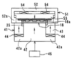
この実施の形態の半導体樹脂封止装置30は、対向して配置された2つの金型、すなわち、第1の金型11と昇降可能な第2の金型31とから構成され、これら2つ金型の間に被成形品15を配置するようになっている。
【0021】
上記第2の金型31は枠状金型34と圧縮金型33から構成され、これらと第1の金型11等の内部には図示しないがヒータを備え、このヒータで封止用樹脂17を加熱溶融するようになっている。これら枠状金型34と圧縮金型33は図示しない昇降機構により昇降するようになっている。また、枠状金型34の枠内には上下に貫通する矩形の貫通孔32が開けられ、その中に圧縮金型33が嵌め込まれている。
【0022】
枠状金型34の上部の内側面には、その外周部の寸法がキャビティCの外周部の寸法(L01×L02)(図29参照)に相当する段部35を設けている。この段部35の底面35aは、圧縮金型33の上面を封止樹脂部18aの表面から分離するときに成形品を保持する保持部となっている。次に、この半導体樹脂封止装置30による樹脂封止方法を説明する。まず、第1の金型11と第2の金型31とを図1に示すように対向して配置する。封止用樹脂17を圧縮金型33の上面に載置し、被成形品15を枠状金型34の上面に載置して、図示しないヒータにより封止用樹脂17を加熱し溶融状態にする。
【0023】
しかる後、圧縮金型33とともに枠状金型34を図示しない昇降機構により図2に示すように上昇させ、枠状金型34の上面と第1の金型11の下面とで被成形品15の配線基板14の周縁部をクランプする。
【0024】
このクランプ後、昇降機構により圧縮金型33をさらに図2に示すように上昇させ、この圧縮金型33で溶融した封止用樹脂17を押しつぶすことによって、配線基板14と枠状金型34と圧縮金型33で形成されるキャビティC内に溶融した封止用樹脂17を充満させることで樹脂封止された成形品18が完成する。
【0025】
樹脂封止後、まず、昇降機構にて圧縮金型33を図3に示すように下降させる。この下降により圧縮金型33の上面を成形品18の封止樹脂部表面18baから分離し離型する。
【0026】
次に、枠状金型34と圧縮金型33とを図4に示すように昇降機構にて第1の金型11から下降させることによって成形品18の配線基板14の上面が第1の金型11の下面から分離する。この後、再度圧縮金型33を図5に示すように上昇させ、成型品18を第2の金型31からエジェクトし成形品を取り出す。
【0027】
離型のとき、圧縮金型33と封止樹脂部18aの図2に示す封止樹脂部表面18baの密着力により、被成形品15と封止樹脂部18aとの樹脂界面18bbにも離型荷重が掛かるが、枠状金型34の貫通孔32に設けた段部35の底面35aが保持部となって封止樹脂部18aの周縁部を下から保持するためこの離型荷重を緩和する。
【0028】
このように、成形品18を保持した状態で離型することで、圧縮金型33の上面と封止樹脂部18aの下面との離型荷重が配線基板14や半導体チップ13にかかるのを最小限に押さえることができるので、離型の際に樹脂界面18bbにおける封止樹脂部18aと配線基板14との剥離を防ぐことができ、良質な成形品を供給することができる。
【0029】
(第2の実施の形態)
次に、図6ないし図9を参照して本発明の第2の実施の形態を説明する。ここでは第1の実施の形態の半導体樹脂封止装置30と同一部分は同一符号をもって説明する。
【0030】
この実施の形態の半導体樹脂封止装置40は第1の金型11と第2の金型41が対向して配置され、この第2の金型41は枠状金型43と圧縮金型42から構成されている。これら枠状金型43、圧縮金型42、第1の金型11等の内部には、封止用樹脂17を加熱溶融するための図示しないヒータを備えている。また、圧縮金型42は昇降機構45により昇降するようになっている。
【0031】
枠状金型43は枠内に上下に貫通する矩形の貫通孔32が開けられており、この貫通孔32によって圧縮金型42の外側に嵌め込まれている。圧縮金型42はその垂直断面が凸字の形状で下部は突起状もしくは鍔状の下腕部42aとなっている。この下腕部42aと枠状金型43との間には、枠状金型43を上げる方向へ反力を発生させる第1の弾性体44が設けられている。枠状金型43はこの第1の弾性体44を介して圧縮金型42の下腕部42aに上方に支持されている。したがって、枠状金型43は昇降機構45により圧縮金型42と連動して昇降するようになっている。
【0032】
枠状金型43の上部の内側面にはその外周部の寸法がキャビティCの外周部の寸法(L01×L02)に相当する段部35を設けている。この段部35の底面35aは圧縮金型42の上面を封止樹脂部18aの表面から分離するときに成形品を保持する保持部となっている。
次に、この半導体樹脂封止装置40による樹脂封止方法を説明する。まず、封止用樹脂17、被成形品15を図6に示すように圧縮金型42、枠状金型43に載置し、封止用樹脂17を図示しないヒータにより加熱溶融する。
【0033】
次に、図7に示すように昇降機構45により圧縮金型42を上昇する。この上昇により枠状金型43が第1の弾性体44を介して圧縮金型42の下腕部42aに押し上げられて上昇し、被成形品15の配線基板14の上面が第1の金型11の下面に当接する。当接後、さらに、第1の弾性体44の弾性力に抗して図8に示すように昇降機構45により圧縮金型42を上昇すると、第1の弾性体44が圧縮し配線基板14に所定のクランプ力を与える。それと同時に圧縮金型42が溶融した封止用樹脂17を押しつぶして被成形品15の表面に均一に圧縮成形し、被成形品15に封止用樹脂17を樹脂封止して成形品18を完成する。
【0034】
樹脂封止後、昇降機構45により圧縮金型42を図9に示すように下降させて圧縮金型42の上面を成形品18の封止樹脂部18aの下面から分離して離型する。このとき、第1の弾性体44は前記離型荷重以上の弾性力で第1の金型11と枠状金型43の段部35の底面35aとの間に成形品18を保持している。
【0035】
この後さらに、昇降機構45にて圧縮金型42を下降させ成形品18、枠状金型43を第1の金型11から分離する。分離が終了したら、たとえば、図示しない真空吸着装置などで成形品18を吸着し第2の金型41から半導体樹脂封止装置40外へ搬出する。
【0036】
このようにすると、圧縮金型42の上面が封止樹脂部表面18baから離型するとき、第1の実施の形態と同様に段部35の底面35aが保持部となって封止樹脂部18aの周縁部を保持するため、離型荷重を緩和するので、樹脂界面18bbでの剥離を防止することができ、良質な成形品を供給できる。さらに、この圧縮成形時等の圧縮金型42、枠状金型43の昇降を、第1の弾性体44を介して1つの昇降機構45により操作できるから昇降機構を簡略化することができる。
【0037】
(第3の実施の形態)
次に、図10ないし図14を参照して本発明の第3の実施の形態を説明する。この第3の実施の形態の半導体樹脂封止装置50は第2の実施の形態の半導体樹脂封止装置40の第1の金型に可動金型板53を設けて改良し成形品のエジェクトを確実にするようにしたものである。
【0038】
この半導体樹脂封止装置50の第1の金型51はホルダ部52aを有する第1の金型本体52と、このホルダ部52aに昇降自在に取り付けられた可動金型板53と、両者の間にあって可動金型板53を下方向に押し付けている第2の弾性体54とで構成されている。この第2の弾性体54は樹脂封止時の下型からの反力より強い初圧でセットされている。
【0039】
次に、この半導体樹脂封止装置50による樹脂封止方法を説明する。図10から図13における一連の動作は第2の実施の形態と同じなのでここでは省略する。図13で圧縮金型42の上面と成形品18の封止樹脂部18aの下面を分離した後、再び昇降機構45にて圧縮金型42を封止樹脂部18aの下面に当接するまで上昇させる。さらに圧縮金型42を上昇させると、昇降機構45の押し上げ力が成形品18を介して可動金型板53に伝わり、第2の弾性体54を撓ませながら第2の金型41の枠状金型43の上面と第1の金型本体52のホルダ部52aの下面が当接する。ここから圧縮金型42を図14の位置まで上昇させ封止樹脂部18aの側面と枠状金型43の内面を離型する。これら一連の動作において成形品18はキャビティ面から完全に離型する。
その後、昇降機構45にて圧縮金型42、枠状金型43、成形品18を下げ、図示しない真空吸着装置などで成形品18を取り出す。
【0040】
この第3の実施の形態によれば、圧縮金型42が封止樹脂部18aの下面から離型するときに発生する樹脂界面18bbでの剥離を第1の実施の形態と同様に防止することができるとともに、この圧縮成形時等の圧縮金型42と枠状金型43の昇降を、第1の弾性体44を介して1つの昇降機構45により昇降できることから昇降機構を簡略化することができる。また、成形品18の側面を枠状金型43の内側面から離型しておくため、成形品18を図示しない真空吸着装置などで取り出すときの離型荷重が殆どなく、真空吸着装置を簡素化できる他、取り出し時の成形品18へのダメージを防止することができる。
【0041】
また、一連の動作において、先に図14の動作を行った後、図13のごとく圧縮金型42の上面と封止樹脂部18aの下面の分離を行っても同様の効果が得られる。
【0042】
(第4の実施の形態)
次に、図15を参照して本発明の第4の実施の形態を説明する。これは第3の実施の形態の変形例で、以下に示す第1の金型61の構成以外は第3の実施の形態と同様である。この実施の形態の半導体樹脂封止装置60の第1の金型61は第1の金型本体62と第1の金型本体62から下方に伸びたストッパピン63、このストッパピン63に挿入され昇降自在に保持された可動金型板64、および両者の間にあって可動金型板64を下方向に押し付けている第2の弾性体65とで構成されている。この第2の弾性体65は樹脂封止時の下型からの反力より強い初圧でセットされている。ここで、第3の実施の形態との違いは、第1の金型本体52のホルダ部52aの代わりに、ストッパピン63に設けられた鍔部63aで可動金型板64の下方向への移動を抑制している点と、成形品18の側面と第2の金型41の枠状金型43の内面との離型時に枠状金型43が上昇するのをストッパピン63の下面で抑制している点である。従って、作用、効果は第3の実施の形態と略同様であるが、本発明では第1の金型をより簡易に構成することができる。
【0043】
(第5の実施の形態)
次に、図16ないし図22を参照して本発明の第5の実施の形態を説明する。なお、従来の半導体樹脂封止装置10と同一部分には同一符号付して説明する。この実施の形態の半導体樹脂封止装置70の第2の金型71は圧縮金型73と枠状金型77と可動ブロック76で構成され、これら圧縮金型73と枠状金型77は図示しない昇降機構により昇降するようになっている。また、枠状金型77の枠内には上下に貫通する矩形の貫通孔72が開けられ、その中に圧縮金型73が嵌め込まれている。
【0044】
圧縮金型73の上部外周には切り込み部74を設け、その上部の上部切り込み部74aは浅く切り込まれ、下部の下部切り込み部74bは上部切り込み部74aより深く切り込まれている。圧縮金型73と枠状金型77の間には、可動ブロック76が上部切り込み部74aと枠状金型77の貫通孔72に嵌合して昇降自在に配置されている。可動ブロック76は切り込み部74内に設けられたばね等の弾性体の支持弾性体75を介して圧縮金型73の下腕部73aの上面に上方に支持され、圧縮金型73の昇降に連動して昇降できるようになっている。このときの支持弾性体75の弾性力は所定の封止圧力付近にセットされている。圧縮金型73、枠状金型77、第1の金型11の内部には図示しないがヒータが備えられ、封止用樹脂17を加熱して溶融するようになっている。
【0045】
次に、この半導体樹脂封止装置70による樹脂封止方法を説明する。まず、図16に示すように圧縮金型73の上面に封止用樹脂17を載置し、枠状金型77の上面には被成形品15を載置して、図示しないヒータにより封止用樹脂17を加熱溶融する。しかる後、圧縮金型73とともに枠状金型77を図示しない昇降機構により図17に示すように上昇させ、枠状金型77の上面と第1の金型11の下面とで被成形品15の配線基板14の周縁部をクランプする。
【0046】
このクランプ後、昇降機構にて圧縮金型73を所定の位置まで上昇させ、キャビティC内に溶融した封止用樹脂17を充満させることで樹脂封止がなされ、樹脂封止された成形品18が完成する。
【0047】
このとき、可動ブロック76は支持弾性体75を介して下腕部73aに押し上げられて上昇するが、封止用樹脂17の投入量の増減により、図17から図19の範囲内で支持弾性体75により所定の樹脂封止圧力を加えられる位置で停止する。例えば、可動ブロック76に支持弾性体75のセット圧以上の樹脂封止圧力が加わることで、図18に示すように支持弾性体75を撓ませながら可動ブロック76が圧縮金型73に対して相対的に下方向に移動し、キャビティ内を所定の封止圧力に維持する。つまり、封止用樹脂17の量が所定量より多い場合には、枠状金型77の上部内側面と圧縮金型73の上部外周面と可動ブロック76の上面76aが形成する凹部78がキャビティの容積を増加させて、この凹部78が多すぎた余分の樹脂を吸収して樹脂封止が完了する。
【0048】
また、樹脂17が所定量より少ない場合は、所定の封止圧力では図19に示すように可動ブロック76の上部76bが圧縮金型73の上面より上に突出した状態になり、キャビティの容積を減少させた状態で樹脂封止が完了する。
【0049】
図17ないし図19の状態で樹脂封止が完了した後、支持弾性体75の反力により可動ブロック76を介して成形品18を第1の金型11に当接しつつ圧縮金型73を図20に示すように昇降機構により下降させ、圧縮金型73の上面を封止樹脂部18aの下面から分離し離型する。
【0050】
この離型のとき、圧縮金型73の上面と封止樹脂部18aの下面との密着力により、被成形品15と封止樹脂部18aとの樹脂界面18bbにも離型荷重が掛かるが、可動ブロック76の上面76aが保持部となって封止樹脂部18aの周縁部を保持するため、樹脂界面18bbに掛かる離型荷重を緩和する。特に封止樹脂部18aの周縁部では、この剥離荷重荷重を極小にすることができる。
【0051】
しかる後、図21に示すように昇降装置にて枠状金型77、圧縮金型73、可動ブロック76、成形品18を第1の金型11から下降させる。その後、図22に示すように圧縮金型73を再度上昇させ、成形品18を第2の金型71からエジェクトする。
【0052】
本実施の形態では、圧縮金型73の上面と封止樹脂部18aの下面との離型荷重が配線基板14や半導体チップ13に掛かるのを最小限に押さえることができるので、離型の際の樹脂界面18bbでの剥離を防ぐことができ、良質な成形品を供給することができる。
【0053】
また、供給する封止用樹脂量が所定量より増減した場合でも、可動ブロック76の可動範囲内(図17から図19の様な位置)であれば所定の封止圧力を保ちつつ成形することが可能である。言い換えれば、供給する樹脂量は可動ブロック76の可動範囲でカバーできる体積分変動してもよいことになり、供給する封止用樹脂量の計量精度を緩和することが可能である。
【0054】
また、可動ブロック76は支持弾性体75を介して圧縮金型73とともに昇降するので特別な昇降機構を必要とせず、装置を簡単にすることができる。
【0055】
なお、この可動ブロック76は環状の一体ものでもよいし、縦に分割された複数のものでもよい。また、本実施の形態では可動ブロック76は支持弾性体75を介して圧縮金型73の下腕部73aに支持されて移動させるようにしたが、圧縮金型とは別の独立した昇降機構に取り付けて移動させるようにしてもよい。
【0056】
また、可動ブロック76、支持弾性体75は圧縮金型73側の切り込み部74内で昇降するが、枠状金型内に同様の切り込みを設けて、枠状金型と連動して昇降するようにしても同様の効果を得ることができる。
【0057】
(第6の実施の形態)
次に、図23を参照して本発明の第6の実施の形態を説明する。これは、以下に示す第2の金型81の構成以外は第5の実施の形態と同様である。この実施の形態の半導体樹脂封止装置80の第2の金型81は、圧縮金型83と枠状金型87と可動ブロック86で構成され、これら圧縮金型83と枠状金型87は図示しない昇降機構により昇降するようになっている。また、枠状金型87の枠内には上下に貫通する貫通孔82が開けられ、その中に圧縮金型83が嵌め込まれている。枠状金型87の上部の内側面には、その外周部の寸法がキャビティCの外周の寸法に相当する段部85を設けている。段部85の底面には上下に貫通する1つもしくは複数の可動ブロック挿入孔88が開けられている。この可動ブロック挿入孔88の下部にはねじ溝が切られ、蓋部87aが下から螺合されている。
【0058】
この可動ブロック挿入孔88に嵌合してピン状の可動ブロック86が昇降自在に配置されている。可動ブロック86は、支持弾性体75を介して枠状金型87の蓋部87aの上面に上方に支持され、枠状金型87の昇降に連動して昇降できるようになっている。このときの支持弾性体75の弾性力は所定の封止圧力付近にセットされている。
【0059】
ここで、第5の実施の形態との違いは、枠状金型87に可動ブロック挿入孔88を設け、可動ブロック86がこの可動ブロック挿入孔88に嵌合して昇降するようになっている点である。従って、作用、効果は第5の実施の形態と略同様である。例えば、図23は封止用樹脂が所定量より多い場合に樹脂封止がなされた状態を示しているが、可動ブロック挿入孔88の上部の凹部89が余分の樹脂の体積を吸収するようになっている。圧縮金型83を封止樹脂部18aから分離するときには、可動ブロック86の上面86aと段部85の底面が封止樹脂部18aに対する保持部となっている。
【0060】
この実施の形態では、枠状金型に可動ブロック挿入孔88を設けたが、圧縮金型に可動ブロック挿入孔を設け、これに可動ブロックと支持弾性体を配置するようにしてもよい。
【0061】
上記各実施の形態では第2の金型を可動にし第1の金型を固定としたが、第1の金型が可動側、第2の金型が固定側でもよいし、第1の金型を下、第2の金型を上にし、被成形品を第1の金型の上に載置して、その上に封止用樹脂を載置してもよい。また、被成形品の樹脂による封止を片方の表面にしたが、これを上下両面に封止してもほぼ同様に実施することはできる。さらに、金型の貫通孔は矩形にしたがこれを丸形、楕円形等にしても同様に実施することができる。
【0062】
さらにまた、第1、第2の弾性体、支持弾性体は、ばねやゴム等の弾性材料のほか被成形品15に応じて空圧装置、油圧装置、小形電動機等を用いた伸縮自在の部材に適宜変更してもほぼ同様に実施することができる。その他被成形品も複数の半導体チップを一体に封止するばかりか1個あるいは2、3個等の少量の単位で封止するものであってもよい。保持部を形成する段部の底面と可動ブロックの上面は水平な面であってもよいし、水平に対して角度を付けた平面や曲面であってもよい。
【0063】
【発明の効果】
本発明は、第1の金型と、この第1の金型に対向して配置され、貫通孔を有する枠状金型とこの貫通孔に嵌合して昇降可能な圧縮金型からなる第2の金型と、前記第1または第2の金型を昇降させる昇降機構とから構成され、これら第1の金型と第2の金型の間に被成形品を配置し、前記第1の金型と枠状金型により被成型品の配線基板の周縁部をクランプし、前記昇降機構により前記圧縮金型が前記第1の金型側へ相対的に移動することで、加熱溶融した封止用樹脂を被成形品に圧縮成形により樹脂封止する半導体樹脂封止装置において、前記第2の金型には、樹脂封止後に前記圧縮金型を成形品から分離するときにこの成形品の封止樹脂周縁部分全部もしくは一部を保持する保持部を設け、圧縮金型を成形品から分離するときに被成形品と圧縮成形した封止樹脂部が剥離しないようにすることができる。
【0064】
また、本発明は、前記圧縮金型を成形品から分離するときにこの成形品の封止樹脂周縁部分全部もしくは一部を保持する保持部としての段部を前記枠状金型または前記圧縮金型に設け、圧縮金型を成形品から分離するときに被成形品と圧縮成形した封止樹脂部が剥離しないようにすることができる。
【0065】
さらに、本発明は、第1の金型と、この第1の金型に対向して配置され、貫通孔を有する枠状金型とこの貫通孔に嵌合して昇降可能な圧縮金型からなる第2の金型と、前記第1または第2の金型を昇降させる昇降機構とから構成され、これら第1の金型と第2の金型の間に被成形品を配置し、前記第1の金型と枠状金型により被成型品の配線基板の周縁部をクランプし、前記昇降機構により前記圧縮金型が前記第1の金型側へ相対的に移動することで、加熱溶融した封止用樹脂を被成形品に圧縮成形により樹脂封止する半導体樹脂封止装置において、前記枠状金型の貫通孔に昇降自在に嵌合させて凸字状の圧縮金型を備え、この圧縮金型の下腕部と前記枠状金型との間に第1の弾性体を設け、前記枠状金型はこの第1の弾性体を介して前記圧縮金型の下腕部に支持されて圧縮金型に連動して1つの昇降機構により昇降するとともに、前記貫通孔の内側面には樹脂封止後に前記圧縮金型を成形品から分離するときにこの成形品の封止樹脂周縁部分全部もしくは一部を保持する保持部としての段部を設け、圧縮金型を成形品から分離するときに被成形品と圧縮成形した封止樹脂部が剥離しないようにするとともに、枠状金型と圧縮金型の相対移動を1つの昇降機構により昇降できるようにすることができる。
【0066】
さらに、本発明は、前記第1の金型には、樹脂封止時に受ける反力より大きい力で圧縮可能な弾性力を有する第2の弾性体と、この第2の弾性体を介して第1の金型本体に昇降可能に保持された可動金属板を備え、成形品のエジェクトを的確に行うようにすることができる。
【0067】
さらに、本発明は、第1の金型と、この第1の金型に対向して配置され、貫通孔を有する枠状金型とこの貫通孔に嵌合して昇降可能な圧縮金型からなる第2の金型と、前記第1または第2の金型を昇降させる昇降機構とから構成され、これら第1の金型と第2の金型の間に被成形品を配置し、前記第1の金型と枠状金型により被成型品の配線基板の周縁部をクランプし、前記昇降機構により前記圧縮金型が前記第1の金型側へ相対的に移動することで、加熱溶融した封止用樹脂を被成形品に圧縮成形により樹脂封止する半導体樹脂封止装置において、圧縮金型の外側面または枠状金型の内側面に切り込み部を設け、この切り込み部に前記貫通孔と前記切り込み部に昇降自在に嵌合して昇降する可動ブロックを備え、この可動ブロックが樹脂封止後に前記圧縮金型を成形品から分離するときにこの成形品の封止樹脂周縁部分全部もしくは一部を保持するようにし、圧縮金型を成形品から分離するときに被成形品と圧縮成形した封止樹脂部が剥離しないようにするとともに、供給する封止用樹脂量の計量精度を緩和するようにすることができる。
【0068】
さらに、本発明は、第1の金型と、この第1の金型に対向して配置され、貫通孔を有する枠状金型とこの貫通孔に嵌合して昇降可能な圧縮金型からなる第2の金型と、前記第1または第2の金型を昇降させる昇降機構とから構成され、これら第1の金型と第2の金型の間に被成形品を配置し、前記第1の金型と枠状金型により被成型品の配線基板の周縁部をクランプし、前記昇降機構により前記圧縮金型が前記第1の金型側へ相対的に移動することで、加熱溶融した封止用樹脂を被成形品に圧縮成形により樹脂封止する半導体樹脂封止装置において、圧縮金型または枠状金型内に可動ブロック挿入孔を設け、この可動ブロック挿入孔に昇降自在に嵌合して昇降する可動ブロックを備え、この可動ブロックが、樹脂封止後に前記圧縮金型を成形品から分離するときにこの成形品の封止樹脂部の周縁部の一部を保持するようにし、圧縮金型を成形品から分離するときに被成形品と圧縮成形した封止樹脂部が剥離しないようにするとともに、供給する封止用樹脂量の計量精度を緩和し、また、可動ブロックを圧縮金型もしくは枠状金型内に入れることで圧縮金型と枠状金型が相対移動する時の影響を可動ブロックが受けないようにすることができる。
【0069】
さらに、本発明は、前記可動ブロックは前記圧縮金型または前記枠状金型に設けられた切り込み部または可動ブロック挿入孔に樹脂封止圧力で圧縮可能な支持弾性体を介して圧縮金型または枠状金型に支持され、この圧縮金型または枠状金型に連動して昇降するようにし、可動ブロックを昇降するための昇降機構を省略して半導体樹脂封止装置の機構を簡略化することができる。
【図面の簡単な説明】
【図1】本発明半導体樹脂封止装置の第1の実施の形態の第1工程を示す説明図。
【図2】本発明半導体樹脂封止装置の第1の実施の形態の第2工程を示す説明図。
【図3】本発明半導体樹脂封止装置の第1の実施の形態の第3工程を示す説明図。
【図4】本発明半導体樹脂封止装置の第1の実施の形態の第4工程を示す説明図。
【図5】本発明半導体樹脂封止装置の第1の実施の形態の第5工程を示す説明図。
【図6】本発明半導体樹脂封止装置の第2の実施の形態の第1工程を示す説明図。
【図7】本発明半導体樹脂封止装置の第2の実施の形態の第2工程を示す説明図。
【図8】本発明半導体樹脂封止装置の第2の実施の形態の第3工程を示す説明図。
【図9】本発明半導体樹脂封止装置の第2の実施の形態の第4工程を示す説明図。
【図10】本発明半導体樹脂封止装置の第3の実施の形態の第1工程を示す説明図。
【図11】本発明半導体樹脂封止装置の第3の実施の形態の第2工程を示す説明図。
【図12】本発明半導体樹脂封止装置の第3の実施の形態の第3工程を示す説明図。
【図13】本発明半導体樹脂封止装置の第3の実施の形態の第4工程を示す説明図。
【図14】本発明半導体樹脂封止装置の第3の実施の形態の第5工程を示す説明図。
【図15】本発明半導体樹脂封止装置の第4の実施の形態を示す説明図。
【図16】本発明半導体樹脂封止装置の第5の実施の形態の第1工程を示す説明図。
【図17】本発明半導体樹脂封止装置の第5の実施の形態の第2工程を示す説明図。
【図18】本発明半導体樹脂封止装置の第5の実施の形態の第2工程の変形例を示す説明図。
【図19】本発明半導体樹脂封止装置の第5の実施の形態の第2工程の他の変形例を示す説明図。
【図20】本発明半導体樹脂封止装置の第5の実施の形態の第3工程を示す説明図。
【図21】本発明半導体樹脂封止装置の第5の実施の形態の第4工程を示す説明図。
【図22】本発明半導体樹脂封止装置の第5の実施の形態の第5工程を示す説明図。
【図23】本発明半導体樹脂封止装置の第6の実施の形態を示す説明図。
【図24】従来の半導体樹脂封止装置の第1工程を示す説明図。
【図25】従来の半導体樹脂封止装置の第2工程を示す説明図。
【図26】従来の半導体樹脂封止装置の第3工程を示す説明図。
【図27】従来の半導体樹脂封止装置の第4工程を示す説明図。
【図28】従来の半導体樹脂封止装置の第5工程を示す説明図。
【図29】一般的な成形品の平面図。
【符号の説明】
10、30、40、50、60、70、80 半導体樹脂封止装置
11、51、61 第1の金型
12、31、41、71、81 第2の金型
13 半導体チップ
14 配線基板
15 被成形品
16、20、45 昇降機構
17 封止用樹脂
18 成形品
18a 封止樹脂部
19、34,43、77、87 枠状金型
19a、32、72、82 貫通孔
21、33、42、73、83 圧縮金型
35 段部
44 第1の弾性体
52、62 第1の金型本体
52a ホルダ部
53、64 可動金型板
54、65 第2の弾性体
63 ストッパピン
74 切り込み部
75 支持弾性体
76、86 可動ブロック
88 可動ブロック挿入孔[0001]
BACKGROUND OF THE INVENTION
The present invention relates to a semiconductor resin sealing device that seals a wiring board (substrate, lead frame) or the like on which a semiconductor chip is mounted with resin.
[0002]
[Background Art and Problems to be Solved by the Invention]
In general, as shown in FIGS. 24 to 28, the semiconductor
[0003]
The
[0004]
Next, the operation of the semiconductor
[0005]
Thereafter, the frame-
[0006]
After this clamping, the
[0007]
After the resin sealing, first, the
[0008]
Next, the frame-
[0009]
At the time of resin sealing, the
[0010]
In the present invention, the resin between the
[0011]
[Means for Solving the Problems]
The invention according to claim 1 is a first mold, a frame-shaped mold that is disposed opposite to the first mold, has a through hole, and a compression mold that can be raised and lowered by fitting into the through hole. And a lifting mechanism for raising and lowering the first or second die, and placing a molded product between the first die and the second die, Clamping the peripheral edge of the wiring board of the molded product by the first mold and the frame-shaped mold, and by moving the compression mold relatively to the first mold side by the lifting mechanism, In a semiconductor resin sealing device that seals a heat-sealed sealing resin to a molded product by compression molding, when the second mold is separated from the molded product after resin sealing A holding portion that holds the peripheral portion of the sealing resin of the molded product, the holding portion of the peripheral portion of the sealing resin of the molded product, Resin interface between the molded product and the second mold The molded article and the compression-molded sealing resin portion are prevented from being peeled off when the compression mold is separated from the molded product.
[0012]
The invention according to claim 2 is characterized in that when the compression mold is separated from the molded product, a stepped portion as a holding portion that holds all or part of the peripheral portion of the sealing resin of the molded product is used as the frame-shaped mold or the compression mold. It is provided in the mold so that the molded article and the compression-molded sealing resin portion are not separated when the compression mold is separated from the molded product.
[0013]
The invention of claim 3 The compression mold has a convex shape fitted to the through hole of the frame-shaped mold so as to be movable up and down, A first elastic body is provided between the lower arm portion of the compression mold and the frame-shaped mold, and the frame-shaped mold is attached to the lower arm portion of the compression mold through the first elastic body. It is supported and moved up and down in conjunction with the compression mold, and when the compression mold is separated from the molded product after resin sealing on the inner surface of the through hole, all or one part of the sealing resin peripheral portion of the molded product A stepped portion is provided as a holding portion for holding the portion, and when the compression mold is separated from the molded product, the molded product and the compression-molded sealing resin portion are prevented from being separated, and the frame-shaped metal The relative movement between the mold and the compression mold can be moved up and down by one lifting mechanism.
[0014]
According to a fourth aspect of the present invention, the first mold includes a second elastic body having an elastic force that can be compressed with a force larger than a reaction force received during resin sealing, and the second elastic body. The first metal mold body is provided with a movable metal plate that can be moved up and down so that the molded product can be ejected accurately.
[0015]
The invention according to claim 5 is a first mold, a frame-shaped mold disposed opposite to the first mold and having a through hole, and a compression mold that can be raised and lowered by fitting into the through hole. And a lifting mechanism for raising and lowering the first or second die, and placing a molded product between the first die and the second die, Clamping the peripheral portion of the wiring board of the molded product by the first mold and the frame-shaped mold, and the compression mold is moved relatively to the first mold side by the lifting mechanism, In a semiconductor resin sealing device for sealing a heat-melted sealing resin to a molded product by compression molding, a notch is provided on the outer surface of the compression mold or the inner surface of the frame mold, and the notch A movable block that moves up and down by fitting to the through hole and the notch is freely movable. When the compression mold is separated from the molded product, all or part of the peripheral portion of the sealing resin of the molded product is retained, and when the compression mold is separated from the molded product, the molded product is compression molded. The sealing resin portion is prevented from peeling off, and the measurement accuracy of the amount of sealing resin to be supplied is relaxed.
[0016]
The invention according to claim 6 is a first mold, a frame-shaped mold that is disposed opposite to the first mold and has a through hole, and a compression mold that can be moved up and down by fitting into the through hole. And a lifting mechanism for raising and lowering the first or second die, and placing a molded product between the first die and the second die, Clamping the peripheral portion of the wiring board of the molded product by the first mold and the frame-shaped mold, and the compression mold is moved relatively to the first mold side by the lifting mechanism, In a semiconductor resin sealing device that seals heat-melted sealing resin to a molded product by compression molding, a movable block insertion hole is provided in the compression mold or frame mold, and the movable block insertion hole is moved up and down. It is equipped with a movable block that can be freely fitted and moved up and down, and this movable block forms the compression mold after resin sealing. When separating from the molded product, a part of the peripheral portion of the sealing resin portion of the molded product is retained, and when the compression mold is separated from the molded product, the molded product and the molded sealing resin portion are not separated. In addition, the measurement accuracy of the amount of sealing resin to be supplied is relaxed, and when the movable block is placed in the compression mold or the frame-shaped mold, the compression mold and the frame-shaped mold are moved relative to each other. The movable block is not affected.
[0017]
According to a seventh aspect of the present invention, the movable block is a compression mold through a support elastic body that can be compressed by a resin sealing pressure in a cut portion or a movable block insertion hole provided in the compression mold or the frame-shaped mold. Or it is supported by a frame-shaped mold and can be moved up and down in conjunction with this compression mold or frame-shaped mold, and the mechanism of the semiconductor resin sealing device is simplified by omitting the lifting mechanism for moving up and down the movable block It is a thing.
[0018]
DETAILED DESCRIPTION OF THE INVENTION
Hereinafter, various preferred embodiments of the present invention will be described with reference to the accompanying drawings.
[0019]
(First embodiment)
A first embodiment of the present invention will be described with reference to FIGS. The same parts as those of the conventional semiconductor
[0020]
The semiconductor
[0021]
The
[0022]
On the inner side surface of the upper part of the frame-shaped
[0023]
Thereafter, the frame-shaped
[0024]
After this clamping, the
[0025]
After the resin sealing, first, the
[0026]
Next, the frame-shaped
[0027]
At the time of mold release, due to the adhesion between the
[0028]
In this way, by releasing the
[0029]
(Second Embodiment)
Next, a second embodiment of the present invention will be described with reference to FIGS. Here, the same parts as those of the semiconductor
[0030]
In the semiconductor
[0031]
The frame-shaped
[0032]
On the inner side surface of the upper part of the frame-shaped
Next, a resin sealing method using the semiconductor
[0033]
Next, as shown in FIG. 7, the
[0034]
After the resin sealing, the
[0035]
Thereafter, the
[0036]
In this way, when the upper surface of the
[0037]
(Third embodiment)
Next, a third embodiment of the present invention will be described with reference to FIGS. The semiconductor
[0038]
The
[0039]
Next, a resin sealing method using the semiconductor
Thereafter, the
[0040]
According to the third embodiment, the separation at the resin interface 18bb that occurs when the
[0041]
Further, in the series of operations, the same effect can be obtained by performing the operation of FIG. 14 first and then separating the upper surface of the
[0042]
(Fourth embodiment)
Next, a fourth embodiment of the present invention will be described with reference to FIG. This is a modification of the third embodiment, and is the same as the third embodiment except for the configuration of the
[0043]
(Fifth embodiment)
Next, a fifth embodiment of the present invention will be described with reference to FIGS. The same parts as those of the conventional semiconductor
[0044]
A
[0045]
Next, a resin sealing method using the semiconductor
[0046]
After this clamping, the
[0047]
At this time, the
[0048]
If the amount of
[0049]
After the resin sealing is completed in the state of FIGS. 17 to 19, the
[0050]
At the time of this release, due to the adhesion between the upper surface of the
[0051]
Thereafter, as shown in FIG. 21, the frame-shaped
[0052]
In the present embodiment, it is possible to minimize the release load between the upper surface of the
[0053]
Further, even when the amount of sealing resin to be supplied is increased or decreased from a predetermined amount, molding is performed while maintaining a predetermined sealing pressure within the movable range of the movable block 76 (position as shown in FIGS. 17 to 19). Is possible. In other words, the amount of resin to be supplied may vary in the volume of the body that can be covered by the movable range of the
[0054]
Further, since the
[0055]
The
[0056]
The
[0057]
(Sixth embodiment)
Next, a sixth embodiment of the present invention will be described with reference to FIG. This is the same as the fifth embodiment except for the configuration of the
[0058]
A pin-shaped
[0059]
Here, the difference from the fifth embodiment is that a movable
[0060]
In this embodiment, the movable
[0061]
In each of the above embodiments, the second mold is movable and the first mold is fixed. However, the first mold may be the movable side and the second mold may be the fixed side. The mold may be on the bottom, the second mold on the top, the product to be molded may be placed on the first mold, and the sealing resin may be placed thereon. Further, although the molded product is sealed with resin on one surface, it can be carried out in substantially the same manner even if this is sealed on both upper and lower surfaces. Further, although the through hole of the mold is rectangular, it can be similarly implemented even if it is round, oval or the like.
[0062]
Furthermore, the first and second elastic bodies and the support elastic body are elastic members using a pneumatic device, a hydraulic device, a small electric motor or the like in accordance with the molded
[0063]
【The invention's effect】
The present invention comprises a first mold, a frame-shaped mold disposed opposite to the first mold and having a through hole, and a compression mold that can be raised and lowered by fitting into the through hole. 2 molds and an elevating mechanism for raising and lowering the first or second mold, and a molded product is disposed between the first mold and the second mold, and the first The peripheral part of the wiring substrate of the molded product is clamped by the mold and the frame-shaped mold, and the compression mold is moved relatively to the first mold side by the lifting mechanism, so that it is heated and melted. In a semiconductor resin sealing apparatus that seals a sealing resin to a molded product by compression molding, the second mold is formed when the compression mold is separated from the molded product after resin sealing. A holding part that holds all or part of the peripheral part of the sealing resin of the product is provided, and when the compression mold is separated from the molded product, Can sealing resin portion was reduced molding to prevent delamination.
[0064]
Further, the present invention provides a stepped portion as a holding portion for holding all or part of the sealing resin peripheral portion of the molded product when the compressed mold is separated from the molded product. When the compression mold is provided from the mold and separated from the molded product, the molded product and the compression-molded sealing resin portion can be prevented from peeling off.
[0065]
Furthermore, the present invention includes a first mold, a frame-shaped mold disposed opposite to the first mold and having a through hole, and a compression mold that can be raised and lowered by fitting into the through hole. A second mold, and a lifting mechanism for raising and lowering the first or second mold, and placing a product to be molded between the first mold and the second mold, Clamping the peripheral portion of the wiring board of the molded product with the first mold and the frame-shaped mold, and the compression mold is relatively moved toward the first mold by the lifting mechanism, thereby heating In a semiconductor resin sealing device for sealing a molten sealing resin to a molded product by compression molding, a convex-shaped compression mold is provided by being fitted to the through hole of the frame-shaped mold so as to be movable up and down. A first elastic body is provided between the lower arm portion of the compression mold and the frame-shaped mold, and the frame-shaped mold is compressed through the first elastic body. This is supported by the lower arm of the mold and is moved up and down by one lifting mechanism in conjunction with the compression mold, and when the compression mold is separated from the molded product after resin sealing on the inner surface of the through-hole, Provide a step as a holding part to hold all or part of the sealing resin peripheral part of the molded product, so that the molded product and the compression molded sealing resin part do not peel when separating the compression mold from the molded product In addition, the relative movement of the frame-shaped mold and the compression mold can be raised and lowered by one lifting mechanism.
[0066]
Further, according to the present invention, the first mold includes a second elastic body having an elastic force compressible with a force larger than a reaction force received at the time of resin sealing, and a second elastic body via the second elastic body. A movable metal plate that can be moved up and down is provided on one mold body, and the molded product can be ejected accurately.
[0067]
Furthermore, the present invention includes a first mold, a frame-shaped mold disposed opposite to the first mold and having a through hole, and a compression mold that can be raised and lowered by fitting into the through hole. A second mold, and a lifting mechanism for raising and lowering the first or second mold, and placing a product to be molded between the first mold and the second mold, Clamping the peripheral portion of the wiring board of the molded product with the first mold and the frame-shaped mold, and the compression mold is relatively moved toward the first mold by the lifting mechanism, thereby heating In a semiconductor resin sealing device for sealing a molten sealing resin to a molded product by compression molding, a cut portion is provided on an outer surface of a compression mold or an inner surface of a frame-shaped mold, and the cut portion is provided with the above-described cut portion. It has a movable block that can be moved up and down by fitting it through the through hole and the notch, and this movable block is resin-sealed. When the compression mold is separated from the molded product, all or part of the peripheral portion of the sealing resin of the molded product is retained, and when the compression mold is separated from the molded product, the molded product is compression molded. While preventing the sealing resin part from peeling off, the measurement accuracy of the amount of sealing resin to be supplied can be relaxed.
[0068]
Furthermore, the present invention includes a first mold, a frame-shaped mold disposed opposite to the first mold and having a through hole, and a compression mold that can be raised and lowered by fitting into the through hole. A second mold, and a lifting mechanism for raising and lowering the first or second mold, and placing a product to be molded between the first mold and the second mold, Clamping the peripheral portion of the wiring board of the molded product with the first mold and the frame-shaped mold, and the compression mold is relatively moved toward the first mold by the lifting mechanism, thereby heating In a semiconductor resin sealing device that seals molten sealing resin to a molded product by compression molding, a movable block insertion hole is provided in the compression mold or frame mold, and the movable block insertion hole can be raised and lowered freely. And a movable block that moves up and down by fitting into the mold. When separating from the molded product, a part of the peripheral portion of the sealing resin portion of the molded product is held, and when the compression mold is separated from the molded product, the molded product and the compression molded sealing resin portion do not peel off. In addition, the measurement accuracy of the amount of sealing resin to be supplied is eased, and when the compression mold and the frame mold move relative to each other by placing the movable block in the compression mold or the frame mold It is possible to prevent the movable block from being affected.
[0069]
Further, according to the present invention, the movable block may be a compression mold or a cut-out part provided in the compression mold or the frame-shaped mold or a movable block insertion hole through a support elastic body that can be compressed with a resin sealing pressure. The mechanism of the semiconductor resin sealing device is simplified by being supported by the frame-shaped mold and moving up and down in conjunction with the compression mold or the frame-shaped mold, and omitting the lifting mechanism for moving up and down the movable block. be able to.
[Brief description of the drawings]
FIG. 1 is an explanatory view showing a first step of a first embodiment of a semiconductor resin sealing device of the present invention.
FIG. 2 is an explanatory view showing a second step of the first embodiment of the semiconductor resin sealing device of the present invention.
FIG. 3 is an explanatory view showing a third step of the first embodiment of the semiconductor resin sealing device of the present invention.
FIG. 4 is an explanatory view showing a fourth step of the first embodiment of the semiconductor resin sealing device of the present invention.
FIG. 5 is an explanatory view showing a fifth step of the first embodiment of the semiconductor resin sealing device of the present invention.
FIG. 6 is an explanatory view showing a first step of the second embodiment of the semiconductor resin sealing device of the present invention.
FIG. 7 is an explanatory view showing a second step of the second embodiment of the semiconductor resin sealing device of the present invention.
FIG. 8 is an explanatory view showing a third step of the second embodiment of the semiconductor resin sealing device of the present invention.
FIG. 9 is an explanatory view showing a fourth step of the second embodiment of the semiconductor resin sealing device of the present invention.
FIG. 10 is an explanatory view showing a first step of the third embodiment of the semiconductor resin sealing device of the present invention.
FIG. 11 is an explanatory view showing a second step of the third embodiment of the semiconductor resin sealing device of the present invention.
FIG. 12 is an explanatory view showing a third step of the third embodiment of the semiconductor resin sealing device of the present invention.
FIG. 13 is an explanatory view showing a fourth step of the third embodiment of the semiconductor resin sealing device of the present invention.
FIG. 14 is an explanatory view showing a fifth step of the third embodiment of the semiconductor resin sealing device of the present invention.
FIG. 15 is an explanatory view showing a fourth embodiment of the semiconductor resin sealing device of the present invention.
FIG. 16 is an explanatory view showing a first step of the fifth embodiment of the semiconductor resin sealing device of the present invention.
FIG. 17 is an explanatory view showing a second step of the fifth embodiment of the semiconductor resin sealing device of the present invention.
FIG. 18 is an explanatory view showing a modification of the second step of the fifth embodiment of the semiconductor resin sealing device of the present invention.
FIG. 19 is an explanatory view showing another modification of the second step of the fifth embodiment of the semiconductor resin sealing device of the present invention.
FIG. 20 is an explanatory view showing a third step of the fifth embodiment of the semiconductor resin sealing device of the present invention.
FIG. 21 is an explanatory view showing a fourth step of the fifth embodiment of the semiconductor resin sealing device of the present invention.
FIG. 22 is an explanatory view showing a fifth step of the fifth embodiment of the semiconductor resin sealing device of the present invention.
FIG. 23 is an explanatory view showing a sixth embodiment of the semiconductor resin sealing device of the present invention.
FIG. 24 is an explanatory view showing a first step of a conventional semiconductor resin sealing device.
FIG. 25 is an explanatory view showing a second step of a conventional semiconductor resin sealing device.
FIG. 26 is an explanatory view showing a third step of a conventional semiconductor resin sealing device.
FIG. 27 is an explanatory view showing a fourth step of a conventional semiconductor resin sealing device.
FIG. 28 is an explanatory view showing a fifth step of a conventional semiconductor resin sealing device.
FIG. 29 is a plan view of a general molded product.
[Explanation of symbols]
10, 30, 40, 50, 60, 70, 80 Semiconductor resin sealing device
11, 51, 61 First mold
12, 31, 41, 71, 81 Second mold
13 Semiconductor chip
14 Wiring board
15 Molded product
16, 20, 45 Lifting mechanism
17 Sealing resin
18 Molded products
18a Sealing resin part
19, 34, 43, 77, 87 Frame mold
19a, 32, 72, 82 Through hole
21, 33, 42, 73, 83 Compression mold
35 steps
44 First elastic body
52, 62 First mold body
52a Holder part
53, 64 Movable mold plate
54, 65 second elastic body
63 Stopper pin
74 Notch
75 Supporting elastic body
76, 86 Movable block
88 Movable block insertion hole
Claims (7)
前記第2の金型には、樹脂封止後に前記圧縮金型を成形品から分離するときにこの成形品の封止樹脂周縁部分を保持する保持部を備え、
前記保持部は、前記成形品の封止樹脂周縁部分のうち、前記成形品と前記第2の金型との樹脂界面に当接して保持することを特徴とする半導体樹脂封止装置。A second mold comprising a first mold, a frame-shaped mold disposed opposite to the first mold and having a through hole, and a compression mold that can be raised and lowered by fitting into the through hole And an elevating mechanism for elevating and lowering the first or second mold, a product to be molded is disposed between the first mold and the second mold, and the first mold Sealing resin which is heated and melted by clamping the peripheral edge portion of the wiring substrate of the molded product with a frame-shaped mold and moving the compression mold relatively to the first mold side by the lifting mechanism. In a semiconductor resin sealing device that seals a molded product with resin by compression molding,
The second mold includes a holding portion that holds a peripheral portion of the sealing resin when the compression mold is separated from the molded product after resin sealing,
The holding part holds and abuts on a resin interface between the molded product and the second mold among the sealing resin peripheral portion of the molded product .
この圧縮金型の下腕部と前記枠状金型との間に第1の弾性体を設け、
前記枠状金型はこの第1の弾性体を介して前記圧縮金型の下腕部に支持されて圧縮金型に連動して昇降するとともに、前記貫通孔の内側面には樹脂封止後に前記圧縮金型を成形品から分離するときにこの成形品の封止樹脂周縁部分全部もしくは一部を保持する保持部としての段部を設けたことを特徴とする請求項1記載の半導体樹脂封止装置。The compression mold has a convex shape fitted to the through hole of the frame-shaped mold so as to be movable up and down,
A first elastic body is provided between the lower arm portion of the compression mold and the frame mold,
The frame-shaped mold is supported by the lower arm portion of the compression mold via the first elastic body, and moves up and down in conjunction with the compression mold, and the inner surface of the through hole is sealed with resin. 2. A semiconductor resin seal according to claim 1, further comprising a step portion as a holding portion for holding all or part of a peripheral portion of the sealing resin of the molded product when the compression mold is separated from the molded product. Stop device.
圧縮金型の外側面または枠状金型の内側面に切り込み部を設け、
この切り込み部に昇降自在に嵌合して昇降する可動ブロックを備え、
この可動ブロックが樹脂封止後に前記圧縮金型を成形品から分離するときにこの成形品の封止樹脂周縁部分全部もしくは一部を保持する保持部であることを特徴とする半導体樹脂封止装置。A second mold comprising a first mold, a frame-shaped mold disposed opposite to the first mold and having a through hole, and a compression mold that can be raised and lowered by fitting into the through hole And an elevating mechanism for elevating and lowering the first or second mold, a product to be molded is disposed between the first mold and the second mold, and the first mold Sealing resin which is heated and melted by clamping the peripheral edge portion of the wiring substrate of the molded product with a frame-shaped mold and moving the compression mold relatively to the first mold side by the lifting mechanism. In a semiconductor resin sealing device that seals a molded product with resin by compression molding,
A notch is provided on the outer surface of the compression mold or the inner surface of the frame mold,
It is equipped with a movable block that can be moved up and down by fitting to this notch,
A semiconductor resin sealing device, wherein the movable block is a holding portion that holds all or part of the peripheral portion of the sealing resin of the molded product when the compression mold is separated from the molded product after resin sealing. .
圧縮金型または枠状金型内に可動ブロック挿入孔を設け、
この可動ブロック挿入孔に昇降自在に嵌合して昇降する可動ブロックを備え、
この可動ブロックが、樹脂封止後に前記圧縮金型を成形品から分離するときにこの成形品の封止樹脂部周縁部分の一部を保持する保持部であることを特徴とする半導体樹脂封止装置。A second mold comprising a first mold, a frame-shaped mold disposed opposite to the first mold and having a through hole, and a compression mold that can be raised and lowered by fitting into the through hole And an elevating mechanism for elevating and lowering the first or second mold, a product to be molded is disposed between the first mold and the second mold, and the first mold Sealing resin which is heated and melted by clamping the peripheral edge portion of the wiring substrate of the molded product with a frame-shaped mold and moving the compression mold relatively to the first mold side by the lifting mechanism. In a semiconductor resin sealing device that seals a molded product with resin by compression molding,
A movable block insertion hole is provided in the compression mold or frame mold,
It is equipped with a movable block that can be moved up and down by fitting in this movable block insertion hole,
The semiconductor resin sealing, wherein the movable block is a holding portion that holds a part of the peripheral portion of the sealing resin portion of the molded product when the compression mold is separated from the molded product after the resin sealing. apparatus.
Priority Applications (1)
| Application Number | Priority Date | Filing Date | Title |
|---|---|---|---|
| JP2001331867A JP3896274B2 (en) | 2001-10-30 | 2001-10-30 | Semiconductor resin sealing device |
Applications Claiming Priority (1)
| Application Number | Priority Date | Filing Date | Title |
|---|---|---|---|
| JP2001331867A JP3896274B2 (en) | 2001-10-30 | 2001-10-30 | Semiconductor resin sealing device |
Publications (2)
| Publication Number | Publication Date |
|---|---|
| JP2003133352A JP2003133352A (en) | 2003-05-09 |
| JP3896274B2 true JP3896274B2 (en) | 2007-03-22 |
Family
ID=19147367
Family Applications (1)
| Application Number | Title | Priority Date | Filing Date |
|---|---|---|---|
| JP2001331867A Expired - Lifetime JP3896274B2 (en) | 2001-10-30 | 2001-10-30 | Semiconductor resin sealing device |
Country Status (1)
| Country | Link |
|---|---|
| JP (1) | JP3896274B2 (en) |
Families Citing this family (13)
| Publication number | Priority date | Publication date | Assignee | Title |
|---|---|---|---|---|
| JP2005150350A (en) * | 2003-11-14 | 2005-06-09 | Renesas Technology Corp | Method for manufacturing semiconductor device |
| JP4301991B2 (en) * | 2004-04-26 | 2009-07-22 | 住友重機械工業株式会社 | Resin sealing method for molded products |
| JP2008137334A (en) * | 2006-12-05 | 2008-06-19 | Sumitomo Heavy Ind Ltd | Resin sealing device |
| JP5153536B2 (en) * | 2008-09-17 | 2013-02-27 | Towa株式会社 | Mold for semiconductor chip compression molding |
| JP5174874B2 (en) * | 2010-09-16 | 2013-04-03 | Towa株式会社 | Compression molding die and compression molding method |
| JP5163721B2 (en) * | 2010-09-17 | 2013-03-13 | 第一精工株式会社 | Resin sealing device and resin sealing method |
| KR101087031B1 (en) * | 2010-10-19 | 2011-11-28 | 신한다이아몬드공업 주식회사 | Encapsulant Forming Apparatus and Method |
| JP5445695B2 (en) * | 2010-12-27 | 2014-03-19 | 日産自動車株式会社 | Semiconductor module, molding apparatus and molding method |
| JP5776092B2 (en) * | 2011-01-11 | 2015-09-09 | アピックヤマダ株式会社 | Compression molding method, compression molding apparatus, and resin supply handler |
| KR101676815B1 (en) | 2011-12-16 | 2016-11-17 | 샌디스크 세미컨덕터 (상하이) 컴퍼니, 리미티드 | Emi shielding and thermal dissipation for semiconductor device |
| JP5826243B2 (en) * | 2013-12-13 | 2015-12-02 | 株式会社郷製作所 | Press molding die and press molding method using the same |
| JP6546767B2 (en) * | 2015-04-06 | 2019-07-17 | アピックヤマダ株式会社 | Resin mold |
| JP6845714B2 (en) * | 2017-03-10 | 2021-03-24 | Towa株式会社 | Resin molding equipment, resin molding method, and manufacturing method of resin molded products |
-
2001
- 2001-10-30 JP JP2001331867A patent/JP3896274B2/en not_active Expired - Lifetime
Also Published As
| Publication number | Publication date |
|---|---|
| JP2003133352A (en) | 2003-05-09 |
Similar Documents
| Publication | Publication Date | Title |
|---|---|---|
| JP3896274B2 (en) | Semiconductor resin sealing device | |
| JP4262468B2 (en) | Resin molding method, resin molding apparatus, and support jig used therefor | |
| JP5817044B2 (en) | Resin sealing device and resin sealing method | |
| US20020025352A1 (en) | Method of resin molding and resin molding machine | |
| KR20060052812A (en) | Resin sealing method of electronic component and mold used for it | |
| EP2177337B1 (en) | Optical device molding system | |
| KR20140007287A (en) | Resin molding machine and method of resin molding | |
| JP4553944B2 (en) | Resin molding method and resin molding apparatus | |
| JP2005219297A (en) | Method and apparatus for molding resin | |
| JP4215593B2 (en) | Resin molding equipment | |
| JP4052939B2 (en) | Resin sealing molding method and apparatus for electronic parts | |
| KR20130007458A (en) | Resin seal molding method of electronic component and apparatus therefor | |
| JP2011046017A (en) | Mold | |
| KR20100001690A (en) | Molding apparatus for manufacturing semi-conductor package | |
| KR102393495B1 (en) | Resin molded product manufacturing method and resin molding apparatus | |
| WO2012128444A1 (en) | Encapsulating material moulding method | |
| JP2005324341A (en) | Resin molding method and resin molding machine | |
| JP2626971B2 (en) | Resin encapsulation molding method and mold for electronic parts | |
| CN103247739B (en) | The press-resin sealing moulding method and apparatus of semiconductor chip | |
| CN116209554B (en) | Method for producing resin molded product | |
| JP3999909B2 (en) | Resin sealing device and sealing method | |
| JP6404734B2 (en) | RESIN MOLDING METHOD, RESIN MOLDING MOLD, AND METHOD FOR PRODUCING MOLDED ARTICLE | |
| JP2022039709A (en) | Resin molding equipment and manufacturing method of resin molded products | |
| US20240009899A1 (en) | Compression mold, resin molding apparatus, resin molding system, and method of manufacturing resin-molded product | |
| TWI874601B (en) | Component sealing method, component sealing device, and method for manufacturing semiconductor product |
Legal Events
| Date | Code | Title | Description |
|---|---|---|---|
| A625 | Written request for application examination (by other person) |
Free format text: JAPANESE INTERMEDIATE CODE: A625 Effective date: 20040513 |
|
| A977 | Report on retrieval |
Free format text: JAPANESE INTERMEDIATE CODE: A971007 Effective date: 20050112 |
|
| A131 | Notification of reasons for refusal |
Free format text: JAPANESE INTERMEDIATE CODE: A131 Effective date: 20060404 |
|
| A521 | Written amendment |
Free format text: JAPANESE INTERMEDIATE CODE: A523 Effective date: 20060605 |
|
| A131 | Notification of reasons for refusal |
Free format text: JAPANESE INTERMEDIATE CODE: A131 Effective date: 20060627 |
|
| A711 | Notification of change in applicant |
Free format text: JAPANESE INTERMEDIATE CODE: A712 Effective date: 20060810 |
|
| A521 | Written amendment |
Free format text: JAPANESE INTERMEDIATE CODE: A523 Effective date: 20060825 |
|
| A521 | Written amendment |
Free format text: JAPANESE INTERMEDIATE CODE: A523 Effective date: 20061107 |
|
| TRDD | Decision of grant or rejection written | ||
| A01 | Written decision to grant a patent or to grant a registration (utility model) |
Free format text: JAPANESE INTERMEDIATE CODE: A01 Effective date: 20061212 |
|
| A61 | First payment of annual fees (during grant procedure) |
Free format text: JAPANESE INTERMEDIATE CODE: A61 Effective date: 20061218 |
|
| R150 | Certificate of patent or registration of utility model |
Ref document number: 3896274 Country of ref document: JP Free format text: JAPANESE INTERMEDIATE CODE: R150 Free format text: JAPANESE INTERMEDIATE CODE: R150 |
|
| S531 | Written request for registration of change of domicile |
Free format text: JAPANESE INTERMEDIATE CODE: R313531 |
|
| FPAY | Renewal fee payment (event date is renewal date of database) |
Free format text: PAYMENT UNTIL: 20091222 Year of fee payment: 3 |
|
| R350 | Written notification of registration of transfer |
Free format text: JAPANESE INTERMEDIATE CODE: R350 |
|
| FPAY | Renewal fee payment (event date is renewal date of database) |
Free format text: PAYMENT UNTIL: 20101222 Year of fee payment: 4 |
|
| FPAY | Renewal fee payment (event date is renewal date of database) |
Free format text: PAYMENT UNTIL: 20101222 Year of fee payment: 4 |
|
| FPAY | Renewal fee payment (event date is renewal date of database) |
Free format text: PAYMENT UNTIL: 20111222 Year of fee payment: 5 |
|
| FPAY | Renewal fee payment (event date is renewal date of database) |
Free format text: PAYMENT UNTIL: 20111222 Year of fee payment: 5 |
|
| FPAY | Renewal fee payment (event date is renewal date of database) |
Free format text: PAYMENT UNTIL: 20121222 Year of fee payment: 6 |
|
| FPAY | Renewal fee payment (event date is renewal date of database) |
Free format text: PAYMENT UNTIL: 20121222 Year of fee payment: 6 |
|
| FPAY | Renewal fee payment (event date is renewal date of database) |
Free format text: PAYMENT UNTIL: 20131222 Year of fee payment: 7 |
|
| S111 | Request for change of ownership or part of ownership |
Free format text: JAPANESE INTERMEDIATE CODE: R313113 |
|
| R350 | Written notification of registration of transfer |
Free format text: JAPANESE INTERMEDIATE CODE: R350 |
|
| R250 | Receipt of annual fees |
Free format text: JAPANESE INTERMEDIATE CODE: R250 |
|
| R250 | Receipt of annual fees |
Free format text: JAPANESE INTERMEDIATE CODE: R250 |
|
| R250 | Receipt of annual fees |
Free format text: JAPANESE INTERMEDIATE CODE: R250 |
|
| EXPY | Cancellation because of completion of term |