JP3854065B2 - Phase compensation clock synchronization circuit - Google Patents
Phase compensation clock synchronization circuit Download PDFInfo
- Publication number
- JP3854065B2 JP3854065B2 JP2000389062A JP2000389062A JP3854065B2 JP 3854065 B2 JP3854065 B2 JP 3854065B2 JP 2000389062 A JP2000389062 A JP 2000389062A JP 2000389062 A JP2000389062 A JP 2000389062A JP 3854065 B2 JP3854065 B2 JP 3854065B2
- Authority
- JP
- Japan
- Prior art keywords
- circuit
- phase
- delay
- output
- clock signal
- Prior art date
- Legal status (The legal status is an assumption and is not a legal conclusion. Google has not performed a legal analysis and makes no representation as to the accuracy of the status listed.)
- Expired - Lifetime
Links
Images


Landscapes
- Pulse Circuits (AREA)
- Stabilization Of Oscillater, Synchronisation, Frequency Synthesizers (AREA)
- Dram (AREA)
Description
【0001】
【発明の属する技術分野】
本発明は、半導体集積回路に用いられる位相補償用のクロック同期回路に係り、特に入力クロック信号と同一周期で位相が異なった出力クロック信号を生成させるために遅延同期ループ(DLL;Delay Locked Loop)あるいは位相同期ループ(PLL;Phase Locked Loop)を用いたクロック同期回路に関するもので、クロック同期型半導体集積回路装置などに使用されるものである。
【0002】
【従来の技術】
位相補償用のDLL 、PLL としては種々のものが提案・使用されてきているが、本発明に特に関するものは、"A Semidigital Dual Delay-Locked Loop", IEEE Journal of Solid-State Circuits, Vol.32,No.11, Nov.1997(論文1)と、"PLL Design for a 500 MB/s Interface", 1993 IEEE International Solid-State Circuits Conference, Digest of Technical Papers, p.160, Feb.1993 (論文2)である。
【0003】
図26は、従来のDLL のブロックダイアグラムを示す。
【0004】
このDLL は、前記論文1に開示されており、コア(Core) DLL110 と周辺(Peripheral) DLL120 の二重のループで構成されていることが特徴である。
【0005】
コアDLL110は、外部クロックExt. Clkが入力し、同じ構成を有する複数の遅延セル10(後述するチャージ・ポンプ回路17の出力電圧によって遅延量が変化する)が直列に接続されてなる遅延線に入力し、この遅延線の各段の遅延セル10から外部クロックExt. Clkの一周期を複数に分割した位相を表現する複数の信号を出力する(外部クロックExt. Clkの一周期を等間隔に分断する分断軸を生成する)役割を有するものである。
【0006】
即ち、コアDLL110は、入力する外部クロックExt. Clkのデューティサイクルを調整するデューティ・サイクル・コレクター回路(duty cycle corrector :DCC)11 と、このDCC11 の出力信号が入力する入力バッファ回路12と、この入力バッファ回路12の出力信号が入力する遅延線13と、この遅延線13の入力の分岐信号が入力する第1のバッファ回路14と、前記遅延線13の出力の分岐信号が入力する第2のバッファ回路15と、第1のバッファ回路14の出力信号C0 と第2のバッファ回路15の出力信号Cπの位相差を検知する位相比較回路(Phase Comp. )16と、この位相比較回路16の出力信号により制御され、出力電圧を遅延セル10に供給するチャージ・ポンプ回路(Charge Pump )17と、このチャージ・ポンプ回路17に供給するバイアス電流を生成するバイアス生成回路(図示せず)とを有する。
【0007】
前記周辺DLL120は、前記コアDLL110で生成された時間的に連続する二軸の信号を選択して混ぜ合わせることにより、外部クロックExt. Clkと同一周期の内部クロックInt. Clkを生成するものである。
【0008】
即ち、周辺DLL120は、コアDLL110の遅延線13を構成する複数の遅延セル10の各出力がバッファ回路20を経て入力し、前記複数の遅延セル10のうちの隣接する2つの遅延セル10の出力を選択する位相選択回路(Phase Selector)21、22と、この位相選択回路21、22からそれぞれバッファ回路23、24を介して取り出したクロック信号Ψ、Φの位相を混合することによって、2つの信号間の位相を反映させた信号(位相補償されたクロック信号)を生成する位相補間回路(Phase Interpolator)25と、この位相補間回路25で生成されたクロック信号が入力し、内部クロックInt. Clkを出力するクロックドライバ回路26と、外部クロックExt. Clkと内部クロックInt. Clkの位相差を検知する位相検知回路(Phase Detector)27と、この位相検知回路27による検出出力に基づいて、位相補間回路25の2入力の混合割合をフィードバック制御するとともに、前記位相選択回路21、22を制御する有限状態遷移機械(Finite State Machine)28を備えている。
【0009】
図27は、従来のPLL のブロックダイアグラムを示す。
【0010】
このPLL は、前記論文2に開示されており、メイン(Main) PLL130 とファイン(Fine) PLL140 の二重のループで構成されていることが特徴である。
【0011】
メインPLL130は、外部クロックExt. Clkが入力し、同じ構成を有する複数の遅延セル30(後述するチャージ・ポンプ回路33の出力電圧によって遅延量が変化する)を含んでループ状に形成される電圧制御発振器(VCO;Voltage Controlled Oscillator)を有し、各段の遅延セル30から外部クロックExt. Clkの一周期を複数に分割した位相を表現する複数の信号を出力する(外部クロックExt. Clkの一周期を等間隔に分断する分断軸を生成する)役割を有する。
【0012】
即ち、メインPLL130は、外部クロックExt. Clkが入力する入力バッファ回路31と、この入力バッファ回路31の出力信号の位相・周波数を検知する位相・周波数検知回路(Phase-Frequency Detector)32と、この位相・周波数検知回路32の出力信号により制御され、出力電圧を遅延セル30に供給するチャージ・ポンプ回路33と、このチャージ・ポンプ回路33から制御電圧が印加される電圧制御発振器34と、この発振器34の最終段の遅延セル30の出力を初段の遅延セル30に帰還するバッファ回路35によりループを形成してなり、このバッファ回路35の出力を前記位相・周波数検知回路32に供給するバッファ回路36を有する。
【0013】
前記ファインPLL140は、前記メインPLL130で生成された時間的に連続する二軸の信号を選択して混ぜ合わせることにより、外部クロックExt. Clkと同一周期の内部クロックInt. Clkを生成する。
【0014】
即ち、ファインPLL140は、メインPLL130の発振器34を構成する複数の遅延セル30の各出力がバッファ回路20を経て入力し、前記複数の遅延セル30のうちの隣接する2つの遅延セル30の出力を選択する位相選択回路21、22と、この位相選択回路21、22からそれぞれバッファ回路23、24を介して取り出したクロック信号Ψ、Φの位相を混合することによって、2つの信号間の位相を反映させた信号(位相補償されたクロック信号)を生成する位相補間回路25と、この位相補間回路25で生成されたクロック信号が入力し、内部クロックInt. Clkを出力するクロックドライバ回路26と、外部クロックExt. Clkと内部クロックInt. Clkの位相差を検知する位相検知回路27と、この位相検知回路27による検出出力に基づいて、位相補間回路25の2入力の混合割合をフィードバック制御するとともに、前記位相選択回路21、22を制御する有限状態遷移機械(Finite State Machine)28を備えている。
【0015】
以下、上記構成について詳細を述べる。
【0016】
図33は、図26中のチャージ・ポンプ回路17の一例を示しており、前記論文1で引用されている" Low-Jitter Process-Independent DLL and PLL Based on Self-Biased Techniques ", IEEI Journa1 of Solid-State Circuits, Vo1.31,No.11, Nov.1996(論文3)に開示されているSelf-Biased Technique を用いている。つまり、チャージ・ポンプ、バイアス回路、遅延セルの回路形式をできるだけ同構成になるようにしてある。
【0017】
このチャージ・ポンプ回路は、図26中の位相比較回路16の出力Up、Dnおよび図34に示すバイアス生成回路からのバイアス電位Vcp 、Vcn を受け、Upが"H" の時は出力Vco を"L" にしようとし、Dnが"H" の時は出力Vco を"H" にしようとする。
【0018】
図34は、図33のチャージ・ポンプ回路ヘバイアス電流を供給するバイアス生成回路の一例を示しており、前記論文3に開示されているSelf-Biased Technique を用いている。
【0019】
このバイアス生成回路は、図33のチャージ・ポンプ回路33の出力Vco を受け、バイアス電位Vcp 、Vcn を生成する。Vco が"L" になれば、Vcp が"L" 、Vcn が"H" となり、バイアス電流を増大させる。Vco が"H" になれば、Vcp が"H" 、Vcn が"L" となり、バイアス電流を減少させる。
【0020】
図42は、図26中/図27中の遅延セルの一例を示しており、前記論文3に開示されているSelf-Biased Technique を用いている。Vcp が"L" 、Vcn が"H"となり、バイアス電流が増大すると、遅延セルの遅延量、つまり入力Vi+/Vi- を受けてから、出力Vo+/Vo- を出力するまでの時間は減少する。Vcp が"H" 、Vcnが"L" となり、バイアス電流が減少すると、遅延セルの遅延量、つまり入力Vi+/Vi- を受けてから、出力Vo+/Vo- をo 出力するまでの時間は増大する。
【0021】
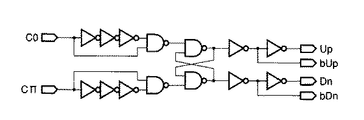
図35は、図26中のコア DLL110 の位相比較回路16の一例を示しており、前記論文1に開示されている。
【0022】
この位相比較回路は、比較入力C0 が"H" になってから比較入力Cπが"H" になるまでの期間は比較出力Upが"H" 、Dnが"L" になり、Cπが"H" になってからC0 が"H" になるまでの期間は比較出力Dnが"H" 、Upが"L" になる。
【0023】
図36乃至図38は、図26中のコアDLL 用の位相比較回路の異なる動作例を示す波形図である。
【0024】
即ち、コア DLL110 の遅延線13の遅延時間が延びると、図37に示すように、C0 ="H"になってからCπ="H"になるまでの期間は長くなり、長くなると位相比較回路16によりUp="H"の期間がDn="H" の期間より長くなるので、チャージ・ポンプ回路17から出力するVco は"L" になり、各遅延セル10の遅延量が短くなって遅延線13の遅延時間は短くなる。
【0025】
これに対して、遅延線13の遅延時間が短くなると、図36に示すように、C0 ="H"になってからCπ="H"になるまでの期間は短くなり、短くなると位相比較回路16によりDn="H"の期間がUp="H" の期間より長くなるので、チャージ・ポンプ回路17から出力するVco は"H" になり、各遅延セル10の遅延量が長くなって遅延線13の遅延時間は長くなる。
【0026】
このような動作により、図38に示すように、C0 ="H"になってからCπ="H"になるまでの期間とCπ="H"になってからC0 ="H"になるまでの期間は同じになり、C0,Cπの周期は外部クロックExt. Clkに等しいことから、C0 ="H"になってからCπ="H"になるまでの期間は、外部クロックの一周期の半分となる。つまりC0 とCπの位相差はちょうど180°(πラジアン)となる。
【0027】
図26中の4段の遅延セル10には、チャージ・ポンプ回路17から同一のバイアス電流を供給されているから、各遅延セル10での遅延時間は同じになる。したがって、C0 とCπの位相差を4段の遅延セル10で4等分することになる。C0 とCπの位相差はちょうど180°になっていて、遅延セル10からの出力として相補信号対を出力するようにすれば、外部クロックExt. Clkの一周期を8等分できることになる。
【0028】
図39は、図27中の位相・周波数検知回路(Phase-Frequency Detector)32の一例を示しており、" A PLL Clock Generator with 5 to 11O MHz of Lock Range for Microprocessors", lEEE Journal of Solid-State Circuits,Vo1. 27, No.11, Nov.1992 (論文4)のFig.5 に開示されている。
【0029】
図40は、図39の回路の状態遷移を説明するために示す図である。
【0030】
位相差、周波数を比較する2 入力ref_clk 、fb_clkの"H" から"L"への遷移の時間的な位置関係のみを比較する。ref_clk が"H" から"L"へ遷移したとき、fb_clkがまだ、"H" のままなら、比較出力Up="H" となる。逆にf b_clkが"H" から"L"へ遷移したとき、ref_clk がまだ、"H" のままなら、比較出力Dn="H" となる。
【0031】
即ち、図27中のメイン PLL130 のVCO34 の出力周期が長いと、外部クロックExt.Clk をバッファリングしたref_clk が"H" から"L"へ遷移したとき、VCO34の出力をバッファリングしたfb_clkがまだ、"H" のままとなるので、比較出力Up="H" となり、チャージ・ポンプ回路33の出力Vco は"L" となり、バイアス電流が増大して、VCO34 を構成する各遅延セル30の遅延量は短くなり、VCO34 の出力周期を短くするようにフィードバックする。
【0032】
これに対してメイン PLL130 のVCO34 の周期が短いと、VCO34 の出力をバッファリングしたfb_clkが"H" から"L"へ遷移したとき、外部クロックExt.Clk をバッファリングしたref_clk が、"H" のままとなるので、比較出力Dn="H" となり、チャージ・ポンプ回路33の出力Vco は"H" となり、バイアス電流が減少して、VCO34 を構成する各遅延セル30の遅延量は長くなり、VCO34 の周期を長くするようにフィードバックする。
【0033】
したがって、上記位相・周波数検知回路32により、図27のメインPLL130は外部クロックと周波数を合わせるように動作する。
【0034】
図27中のVCO34 を形成する4段の遅延セル30には、チャージ・ポンプ回路33から同一のバイアス電流を供給されているから、各遅延セル30での遅延時間は同じになる。したがって、遅延セル30からの出力として相補信号対を出力するようにすれば、外部クロックの一周期を8等分できることになる。
【0035】
図28は、図26中の遅延セル10/図27中の遅延セル30の数が4つで、それらの相補信号出力により、外部クロックExt. Clkの一周期を8象限で表わした(8等分した)場合を示す。
【0036】
図26中の周辺DLL120、図27中のファイン PLL140 の位相検知回路(Phase Detector)27の具体的な回路図は示していないが、この位相検知回路27は、前記論文1、2の趣旨から、入力レシーバと同型のものとなる。
【0037】
図24は、上記位相検知回路27の出力波形例を示す。内部クロックInt.Clk が"H" から"L" に遷移した時、外部クロックExt.Clk がまだ"H" なら、入力レシーバと同型の位相検知回路27の出力信号lateは"H" となり、外部クロックExt.Clkの位相に対して、内部クロックInt.Clk の位相は進んでいることを示す。逆に、内部クロックInt.Clk が"H" から"L" に遷移した時、外部クロックExt.Clk が既に"L" なら、入力レシーバと同型の位相検知回路27の出力信号lateは"L" となり、外部クロックExt.Clk の位相に対して、内部クロックInt.Clk の位相は遅れていることを示す。
【0038】
図26中の周辺DLL120、図27中のファイン PLL140 の位相検知回路27を入力レシーバと同型にすることで、入力レシーバでの内部クロックInt.Clk のデータラッチ遅延を周辺DLL120、ファイン PLL140 の位相比較に反映することができるため、データのセットアップ時間、ホールド時間に対するマージンが向上し、より高周波数動作に対応できる。
【0039】
図43は、図26中/図27中の位相補間回路(Phase Interpolator)25 の一例として、前記論文1に開示されているものを示す。
【0040】
この位相補間回路において、Φ+とΦ−、Ψ+とΨ−、Θ+とΘ−はそれぞれ相補信号である。Vcn 、Vcp は図34のバイアス生成回路から供給されるバイアス電圧である。bIctrl<1> とIctrl<1>、…bIctrl<15>とIctrl<15> は、それぞれ相補の重み付け信号である。
【0041】
bIctrl<1> …bIctrl<15>が全て"H" 、Ictrl<1>…Ictrl<15> が全て"L" なら、Φ+とΦ−入力の差動対には電流が流れ、Ψ+とΨ−入力の差動対には電流が流れないので、出力Θ+とΘ−には、Φ+とΦ−の影響のみ現われ、Ψ+とΨ−には影響されない。
【0042】
逆に、bIctrl<1> …bIctrl<15>が全て"L" 、Ictrl<1>…Ictrl<15> が全て"H"なら、Ψ+とΨ−入力の差動対には電流が流れ、Φ+とΦ−入力の差動対には電流が流れないので、出力Θ+とΘ−には、Ψ+とΨ−の影響のみ現われ、Φ+とΦ−には影響されない。
【0043】
bIctrl<1> …bIctrl<15>の"H" の数が多いほど、(Ictrl<1>…Ictrl<15> の"L" の数が多いほど)、出力Θ+とΘ−には、Φ+とΦ- の影響が強く現われ、Ictrl<1>…Ictrl<15> の"H" の数が多いほど、(bIctrl<1> …bIctrl<15>の"L" の数が多いほど)、出力Θ+とΘ−には、Ψ+とΨ- の影響が強く現われる。
【0044】
これにより、(Φ+/Φ−)入力と(Ψ+/Ψ−)入力の位相が混合されて、Φが100 %の影響を及ぼしている位相からΨが100 %の影響を及ぼしている位相の範囲を補間した出力を実現できる。
【0045】
即ち、前記周辺 DLL120 /ファイン PLL140 のFSM 28の出力により、前記位相選択回路21、22で選択された2軸の重みを変えて、2軸間の位相を表現するものであり、16段階の重み付けができるように構成されている。
【0046】
ところで、図43に示した位相補間回路25は、重み付け信号が相補合わせて30あり、均等に重み付けされており、重み付け信号の切り替わり時の電流ノイズが小さく、安定性は良いが、レイアウト面積が大きいという難点がある。
【0047】
図44は、図26中/図27中の位相補間回路25の他の例として、バイナリカウンタ(Binary Counter)の出力をそのまま使って重み付けをバイナリ的に行ったアナログ的な位相補間回路を示す。
【0048】
重み付け信号bCIctrl<0>、CIctrl<0> 入力の電流パスに対して、bCIctrl<1>、CIctrl<1> 入力の電流パスはその2倍、bCIctrl<2>、CIctrl<2> 入力の電流パスはさらにその2倍、bCIctrl<3>、CIctrl<3> 入力の電流パスはさらにその2倍になっている。重み付け信号の切り替わり時に関与する電流値が小さければ、切り替わり時の電流ノイズが小さく、安定性も、これで問題はない。
【0049】
図45は、図26中/図27中の位相補間回路25の入出力特性として、2つの入力Ψ、Φと1つの出力Θとの関係が理想的な場合を概念的に示す。
【0050】
ここでは、分かり易く説明するために、Φの重みが100 %の場合、Φの影響が50%でΨの影響が50%の場合、Ψの重みが100 %の場合を示している。
【0051】
Φの影響が100 %でΨの影響が0 %の場合のΘの位相は最も進んでおり、Ψの影響が100 %でΦの影響が0 %の場合のΘの位相は最も遅れており、Φの影響が50%でΨの影響が50%の場合のΘの位相は前2者の中間の位相となる。
【0052】
ΦとΨの影響の度合を変えることでΘの位相は、Φの影響が100 %でΨの影響が0 %の場合のΘの位相と、Ψの影響が100 %でΦの影響が0 %の場合のΘの位相の間のどれかをとることができる。
【0053】
図46は、図45に示した2つの入力Ψ、Φの混合度合で決まる出力波形の位相(Phase) と、それを制御するためのウエイト(Weight)信号の理想的な関係を示す図である。
【0054】
ここでは、2つの入力Ψ、Φの混合度合(出力Θに対する影響度)をWeight信号によって16段階に変えた場合を示しており、Φの影響が100 %でΨの影響が0 %の場合のΘの位相と、Ψの影響が100 %でΦの影響が0 %の場合のΘの位相の間を16分割した位相を実現できることになる。
【0055】
図49および図50は、図26中/図27中の位相選択回路(Phase Selector)21、22の一例を示しており、前記論文1("A Semidigital Dual Delay-Locked Loop", IEEE Journal of Solid-State Circuits, Vol.32,No.11, Nov.1997)に開示されている。Vcn 、Vcp は図34のバイアス生成回路から供給されるバイアス電圧である。
【0056】
入力sel0/sel0b〜sel3/sel3bは図26中/図27中の有限状態遷移機械28の出力であり、これにより連続する二軸を選択する。例えば、図28においてQ0象限を選択した場合、有限状態遷移機械28の出力として、sel0とsel1が"H" となり、他は"L" となる。sel0が"H" となって、遅延線13/VCO34 の一段目の遅延セルの出力P0/bP0がΦ+/Φ−として出力され、P0軸が選択される。sel1が"H" となって、遅延線13/VCO34 の二段目の遅延セルの出力P1/bP1がΨ+/Ψ−として出力され、P1軸が選択される。この状態で、図26中の周辺DLL120、図27中のファイン PLL140 の位相検知回路(Phase Detector)27が動作し、比較出力を元に、有限状態遷移機械28のWeight信号によって、位相補間回路25はΦとΨを混合する。
【0057】
Q0象限において、内部クロックInt.Clk の位相が外部クロックExt.Clk の位相に合わなかった場合、例えば、内部クロックInt.Clk の位相が外部クロックExt.Clk の位相より遅れている場合は、有限状態遷移機械28によって、Q7象限に移る。このとき、sel0とsel3b が"H" となり、他は"L" となる。sel0が"H" のままであるから、遅延線13/VCO34 の一段目の遅延セルの出力P0/bP0がΦ+/Φ−として出力され、P0軸が選択される。sel3b が"H" となって、遅延線13/VCO34 の四段目の遅延セルの出力bP3/P3がΨ+/Ψ−として出力され、bP3 軸が選択される。上記の説明において位相補間回路の入出力関係は、記号/の前後の順序は同順関係である。
【0058】
内部クロックInt.Clk の位相が外部クロックExt.Clk の位相より進んでいる場合は、有限状態遷移機械28によって、Q2象限に移る。このとき、sel1とsel2が"H" となり、他は"L" となる。sel1が"H" のままであるから、遅延線13/VCO34 の二段目の遅延セルの出力P1/bP1がΨ+/Ψ−として出力され、P1軸が選択される。sel2が"H" となって、遅延線13/VCO34 の三段目の遅延セルの出力P2/bP2がΦ+/Φ−として出力され、P2軸が選択される。
【0059】
以上により、これらの例の二重ループを有するPLL 、DLL の特徴的な所は、二重ループの一方のコアDLL110ないしはメインPLL130で外部クロックの一周期を等分割に分割するための"軸"信号を生成し、生成された軸信号のうち、時間的に連続する二軸の信号を選択して混ぜ合わせることにより、外部クロックExt.Clkと同一周期の内部クロックInt.Clk を生成する。
【0060】
ところで、図26のDLL において、外部クロックExt. Clkの周期が短くてバイアス電流を最大にしてもなお遅延セル10の遅延が大きい場合、C0 とCπの位相差が外部クロックExt. Clkの180 °以上になり、図32に示すように、コアDLL110はクロックの一周期を等間隔に分断できないばかりではなく、ある位相が、二組の軸の混ぜ合わせで表現され、初期値によっては、ロックができたり、できなくなるという問題が発生する。
【0061】
図27のPLL においては、外部クロックExt. Clkの周期が短くてバイアス電流を最大にしてもなお遅延セル30の遅延が大きい場合、メインPLL130のVCO の周期が外部クロックExt. Clkの周期より長くなり、クロックのサイクル数で、二組で表現されるようになる位相が変化していき、事態はより深刻である。
【0062】
この状況で、外部クロックExt. ClkのジッタあるいはEMl 対策のためにクロックの周波数を分散させている場合、一旦はロックしても、ロックポイントからずれる場合があり、DLL/PLL が位相補間する時に前記したように二組で表現される位相にいると、ずれた外部クロックExt. Clkの位相に再ロックするまで、選択する軸を変えなければならない場合があり、その場合は再ロックするまで時間がかかる。
【0063】
上記とは逆に、DLL の外部クロックExt. Clkの周期が長くてバイアス電流を最小にしても遅延セル10の遅延が小さい場合は、C0 とCπの位相差が外部クロックの180 °未満となり、図31に示すように、最終象限の軸間の角度、位相差が大きくなる。すると、図47に示すように、特に二軸を等分に近い状態で混ぜ合わせると、位相補間回路25の出力波形に平坦な部分が生じ、それが増幅段である次段の回路閾値に近いと、ノイズにより、位相が大きく変わることとなる。これにより、図46に示すような理想的な場合に比較して、図48に示すように位相が大きく変化する部分がでる。
【0064】
図27のPLL においては、外部クロックExt. Clkの周期が長くてバイアス電流を最小にしてもなお遅延セル30の遅延が小さい場合、メインPLL130のVCO の周期が外部クロックExt. Clkの周期より短くなり、クロックのサイクル数で、二組で表現されるようになる位相が変化していき、事態はより深刻である。
【0065】
図31は、図26中の遅延セル10/図27中の遅延セル30の数が4つで、それらの相補信号出力により、外部クロックExt. Clkの一周期を8象限で表わした(8等分した)場合であるが、遅延セル10/遅延セル30の遅延が不十分で最終象限の位相が大きくなった場合を示す。
【0066】
図32は、図26中の遅延セル10/図27中の遅延セル30の数が4つで、それらの相補信号出力により、外部クロックExt. Clkの一周期を8象限で表わそうとした場合であるが、遅延セル10/遅延セル30の遅延が過多で外部クロックExt. Clkの一周期を8象限で表わせなかった場合を示す。
【0067】
図47は、図26中/図27中の位相補間回路25の2つの入力Ψ、Φと1つの出力Θとの入出力特性について、Q7象限が選択されていて、2つの入力Ψ、Φの軸間の位相が大きい場合の入出力波形を概念的に示す。ここでは、図45と比較できるように、Φの重みが100 %の場合、Φの影響が50%でΨの影響が50%の場合、Ψの重みが100 %の場合を示している。
【0068】
Φの影響が100 %でΨの影響が0 %の場合のΘの位相は最も進んでおり、Ψの影響が100 %でΦの影響が0 %の場合のΘの位相は最も遅れており、Φの影響が50%でΨの影響が50%の場合のΘの位相は前2者の中間の位相となる。
【0069】
入力Φと入力Ψ間の遅延が大きく、入力Φが"H" に立ち上がりきってから、Ψが到着すると、例えば、Φの影響が50%でΨの影響が50%の場合のΘの出力には平坦な部分が生じてしまう。
【0070】
図26中/図27中の位相補間回路25の出力Θを入力として受けるバッファ26の回路閾値が、この出力Θの平坦部近辺にあると、基板ノイズ、電源線ノイズなどにより、Θの電位がバッファ26の回路閾値に対して上下すると、内部クロックInt.Clk の位相がぶれて、内部クロック出力にジッタがのる。また、図48に示すように、位相の変化の割合が大きくなる。
【0071】
【発明が解決しようとする課題】
上記したように従来の二重ループ型のDLL 、PLL は、従来の一重ループのものと比べて位相合わせができる周波数範囲が広いものの、外部クロックの周期が短くて遅延セルの遅延が大きい場合とか外部クロックの周期が長くて遅延セルの遅延が小さい場合などでは、位相合わせが困難になり、位相合わせができる周波数範囲が狭いという問題があった。
【0072】
本発明は上記の問題点を解決すべくなされたもので、本来の特徴を活かして、位相合わせができる周波数範囲をより広く出来る位相補償用のクロック同期回路を提供することを目的とする。
【0073】
【課題を解決するための手段】
本発明の第1の位相補償用のクロック同期回路は、同じ構成を有する複数の遅延セルが直列に接続されてなり、第1のクロック信号が入力する遅延線と、前記遅延線による前記第1のクロック信号の一周期の分割数を切換可能な第1の切換回路と、前記遅延線に入力する第1のクロック信号と前記第1の切換回路で切換えられた信号との位相差を検知する位相比較回路と、前記位相比較回路の検知結果に基づき前記複数の遅延セルに供給する電圧もしくは電流を制御して前記複数の遅延セルにおける遅延量を可変するチャージ・ポンプ回路と、前記チャージ・ポンプ回路から前記複数の遅延セルに供給される電圧もしくは電流が前記複数の遅延セルの遅延量を制御できる範囲の上限または下限に対応した値に達したことを検知し、これを検知した際に前記第1のクロック信号の一周期の分割数を増加もしくは減少させるように前記第1の切換回路の制御を行う第1の制御回路を有し、前記遅延線の各段の遅延セルから前記第1のクロック信号の一周期を複数に分割した位相を表現する複数の信号を出力する第1の遅延同期ループと、前記第1の遅延同期ループの遅延線を構成する複数の遅延セルのうちの隣接する2つの遅延セルの出力を選択する位相選択回路と、前記位相選択回路の2つの出力信号の位相を混合することによって位相補償されたクロック信号を生成する位相混合回路と、前記位相混合回路で生成されたクロック信号が入力し、第2のクロック信号を出力するクロックドライバ回路と、前記第1のクロック信号と前記第2のクロック信号の位相差を検知する位相検知回路と、前記位相検知回路による検出出力に基づいて前記位相混合回路の2入力の混合割合をフィードバック制御するとともに前記位相選択回路を制御する第2の制御回路を有し、前記位相選択回路の2つの出力信号の位相を混合することにより、前記第1のクロック信号との位相のずれを補償した第2のクロック信号を生成する第2の遅延同期ループとを具備することを特徴とする。
【0074】
本発明の第2の位相補償用のクロック同期回路は、第1のクロック信号が入力し、同じ構成を有する複数の遅延セルがループ状に接続されてなる電圧または電流制御発振器と、前記第1のクロック信号が入力する入力バッファ回路の出力信号と前記電圧または電流制御発振器の出力信号との位相差・周波数差を検知する位相・周波数検知回路と、前記位相・周波数検知回路の出力信号により制御され、制御出力を前記電圧または電流制御発振器内の複数の遅延セルに供給するチャージ・ポンプ回路と、前記電圧または電流制御発振器の遅延セルの実質的に使用する数を切り換える第1の切換回路と、前記チャージ・ポンプ回路から前記複数の遅延セルに供給される制御出力が前記複数の遅延セルの遅延量を制御できる範囲の上限または下限に対応した値に達したことを検知し、これを検知した際に前記第1のクロック信号の一周期の分割数を増加もしくは減少させるように前記第1の切換回路の制御を行う第1の制御回路を有し、前記発振器の各段の遅延セルから前記第1のクロック信号の一周期を複数に分割した位相を表現する複数の信号を出力する第1の位相同期ループと、前記第1の位相同期ループの発振器を構成する複数の遅延セルのうちの隣接する2つの遅延セルの出力を選択する位相選択回路と、前記位相選択回路の2つの出力信号の位相を混合することによって位相補償されたクロック信号を生成する位相混合回路と、前記位相混合回路で生成されたクロック信号が入力し、第2のクロック信号を出力するクロックドライバ回路と、前記第1のクロック信号と前記第2のクロック信号の位相差を検知する位相検知回路と、前記位相検知回路による検出出力に基づいて、前記位相混合回路の2入力の混合割合をフィードバック制御するとともに、前記位相選択回路を制御する第2の制御回路を有し、前記位相選択回路の2つの出力信号の位相を混合することにより、前記第1のクロック信号との位相のずれを補償した第2のクロック信号を生成する第2の位相同期ループとを具備することを特徴とする。
【0075】
【発明の実施の形態】
以下、図面を参照して本発明の実施の形態を詳細に説明する。
【0076】
<第1の実施例>
図1は、本発明の第1の実施の形態に係るDLL を利用した位相補償用のクロック同期回路の第1の実施例を示すブロックダイアグラムである。
【0077】
このクロック同期回路の特徴は、DLL において、コア DLLの遅延セルの使用個数を変えることにより遅延量を変えて位相合わせを行なうものである。つまり、外部クロックExt. Clkの一周期を複数に分割した位相の軸間の角度差、位相差が大きくならないように、遅延セルをコア DLL内に追加したり、コアDLL の遅延線の入力信号C0 と出力信号Cπの位相差が外部クロックの周期の1/2 となるように、遅延セルをコアDLL 内から論理上排除できるようにする。
【0078】
即ち、図1に示すクロック同期回路は、従来例のDLL と同様にコアDLL110a と周辺 DLL120 の二重のループで構成されているが、従来例のDLL と比べて、チャージ・ポンプ(Charge Pump) 回路17の出力Vco の電位を比較する回路を設け、設定値(VcoMax)より高い場合はコアDLL110a の遅延線13に遅延セル10を付加し、設定値(VcoMin)より低い場合は、コアDLL110a の遅延線13から遅延セル10を排除するように変更したものである。
【0079】
上述した遅延セル10の数に応じて外部クロックExt. Clkの一周期の等分数が変化する。つまり、チャージ・ポンプ(Charge Pump) 回路17の出力Vco の最高電位(VcoMax)は、遅延セル10の遅延量がこれ以上増大できない電位として設定し、それを超えた場合は、コアDLL110a の遅延線13に遅延セル10を付加することにより、遅延線13の遅延量を増大して、C0 とCπの位相差が外部クロックExt.Clkの周期の半分になるようにする。逆に、チャージ・ポンプ回路17の出力Vco の最低電位(VcoMin)より低い場合は、遅延セル10の遅延量が減少できない電位として設定し、それを超えた場合は、コアDLL110a の遅延線13から遅延セル10を削除することにより、遅延線の遅延量を減少させて、C0 とCπの位相差が外部クロックExt.Clk の周期の半分になるようにする。
【0080】
なお、図1に示したクロック同期回路の内部回路は、前記論文1に記述のあるものは、それに従い、ないものは補った。
【0081】
コアDLL110a は、外部クロックExt. Clk(第1のクロック信号)が入力し、同じ構成を有する複数の遅延セル10が直列に接続されてなる遅延線13に入力し、この遅延線13の各段の遅延セル10から外部クロックExt. Clkの一周期を複数に分割した位相を表現する複数の信号を出力する(外部クロックExt. Clkの一周期を等間隔に分断する分断軸を生成する)役割を有するものである。
【0082】
即ち、コアDLL110a は、入力する外部クロックExt. Clkのデューティサイクルを調整するデューティ・サイクル・コレクター回路(duty cycle corrector:DCC)11と、このDCC11 の出力信号が入力する入力バッファ回路12と、この入力バッファ回路12の出力信号が入力する遅延線13と、この遅延線13の入力の分岐信号が入力する第1のバッファ回路14と、前記遅延線13の出力の分岐信号が入力する第2のバッファ回路15と、第1のバッファ回路14の出力信号C0 と第2のバッファ回路15の出力信号Cπの位相差を検知する位相比較回路16と、この位相比較回路16の出力信号により制御され、出力電圧を遅延セル10に供給するチャージ・ポンプ回路17と、このチャージ・ポンプ回路17に供給するバイアス電流を生成するバイアス生成回路(図示せず)と、有限状態遷移機械(Finite State Machine)18と、切換回路(Multiplexer; MUX)19を有する。
【0083】
上記有限状態遷移機械18は、前記チャージ・ポンプ回路17の出力により、遅延線13に遅延セル10の論理的な付加・削除を切換回路(Multiplexer; MUX)19を用いて行なう。
【0084】
前記周辺DLL120は、前記コアDLL110a で生成された時間的に連続する二軸の信号を選択して混ぜ合わせることにより、外部クロックExt. Clkと同一周期で位相が異なった内部クロックInt. Clkを生成するものである。
【0085】
即ち、周辺DLL120は、コアDLL110a の遅延線13を構成する複数の遅延セル10の各出力がバッファ回路20を経て入力し、前記複数の遅延セル10のうちの隣接する2つの遅延セル10の出力を選択する位相選択回路21、22と、この位相選択回路21、22からそれぞれバッファ回路23、24を介して取り出したクロック信号Ψ(Ψ+/Ψ- )、Φ(Φ+/Φ- )の位相を混合することによって、2つの信号間の位相を反映させた信号(位相補償されたクロック信号)を生成する位相補間回路25と、この位相補間回路25で生成されたクロック信号が入力し、内部クロックInt. Clkを出力するクロックドライバ回路26と、外部クロックExt. Clkと内部クロックInt. Clkの位相差を検知する位相検知回路27と、この位相検知回路27による検出出力に基づいて、位相補間回路25の2入力の混合割合をフィードバック制御するとともに、前記位相選択回路21、22を制御する有限状態遷移機械(Finite State Machine)28を備えている。
【0086】
上記有限状態遷移機械28は、位相補間回路25の2つの入力ΦとΨの出力Θに対する影響度を例えば16段階のWeightで重み付けするためのWeight信号を生成する回路を含み、位相検知回路27の検知出力に基づいて、Weight信号により、位相補間回路25のΦの位相とΨの位相の出力Θに対するそれぞれの影響度(Φの位相とΨの位相の混ぜ合わせ具合)をフィードバック制御するものである。また、有限状態遷移機械28は、有限状態遷移機械18から遅延線13を構成する遅延セル数の情報を受け取り、隣接する2つの遅延セル10の出力を選択する。
【0087】
<第2の実施例>
図2は、本発明の第2の実施の形態に係るPLL を利用した位相補償用のクロック同期回路の実施例を示すブロックダイアグラムである。
【0088】
このクロック同期回路の特徴は、PLL において、メイン PLLの遅延セルの個数を変えることにより遅延量を変えて位相合わせを行なうものである。つまり、外部クロックExt. Clkの一周期を複数に分割した位相の軸間の角度差、位相差が大きくならないように、遅延セルをメイン PLL内に追加したり、C0 とCπの位相差が外部クロックの周期の1/2 となるように、遅延セルをメイン PLL内から論理上排除できるようにする。
【0089】
即ち、図2に示すクロック同期回路は、従来例のPLL と同様に、メイン PLL130aとファイン PLL140 の二重のループで構成されているが、従来例のPLL に対して、チャージ・ポンプ(Charge Pump) 回路33の出力Vco の電位を比較する回路を設け、設定値(VcoMax)より高い場合はメイン PLL130aの電圧制御発振器のループ内に遅延セル30を付加し、設定値(VcoMin)より低い場合は、メイン PLL130aの電圧制御発振器のループ内から遅延セル30を排除するように変更したものである。上述した遅延セル30の数に応じて外部クロックExt. Clkの一周期の等分数が変化する。
【0090】
このクロック同期回路の内部回路は、前記論文2に記述のあるものは、それに従い、ないものは補った。この場合、図2中の遅延セル30、チャージ・ポンプ回路33は、図1中の遅延セル10、チャージ・ポンプ回路17と共通のものを使う(共通化する)ことにより、図35に示すコア DLL用の位相比較回路16の出力信号を取り替えた。
【0091】
メイン PLL130aは、外部クロックExt.Clk が入力し、同じ構成を有する複数の遅延セル30(後述するチャージ・ポンプ回路33の出力電圧によって遅延量が変化する)を含んでループ状に形成される電圧制御発振器(VCO)を有し、各段の遅延セル30から外部クロックExt. Clkの一周期を複数に分割した位相を表現する複数の信号を出力する(外部クロックExt. Clkの一周期を等間隔に分断する分断軸を生成する)役割を有する。
【0092】
即ち、メインPLL130a は、外部クロックExt. Clkが入力する入力バッファ回路31と、この入力バッファ回路31の出力信号と後述するバッファ回路36からの帰還信号との位相差・周波数差を検知する位相・周波数検知回路(Phase-Frequency Detector)32と、この位相・周波数検知回路32の出力信号により制御され、制御出力を遅延セル30に供給するチャージ・ポンプ回路33と、このチャージ・ポンプ回路33から制御電圧(あるいは制御電流)が印加される電圧制御発振器(あるいは電流制御発振器)34と、この発振器34の最終段の遅延セル30の出力を初段の遅延セル30に帰還するバッファ回路35によりループを形成してなり、このバッファ回路35の出力を前記位相・周波数検知回路32に供給するバッファ回路36と、有限状態遷移機械(Finite State Machine)38と、切換回路(Multiplexer; MUX)39を有する。
【0093】
上記有限状態遷移機械38は、前記チャージ・ポンプ回路33の出力により、電圧制御発振器(VCO) を構成する遅延セル30の論理的な付加・削除を切換回路(Multiplexer; MUX)39を用いて行なう。
【0094】
前記ファインPLL140は、前記メインPLL130a で生成された時間的に連続する二軸の信号を選択して混ぜ合わることにより、外部クロックExt. Clkと同一周期で位相が異なった内部クロックInt.Clk を生成する。
【0095】
即ち、ファインPLL140は、メインPLL130a の発振器34を構成する複数の遅延セル30の各出力がバッファ回路20を経て入力し、前記複数の遅延セル30のうちの隣接する2つの遅延セル30の出力を選択する位相選択回路21、22と、この位相選択回路21、22からそれぞれバッファ回路23、24を介して取り出したクロック信号Ψ(Ψ+/Ψ- )、Φ(Φ+/Φ- )の位相を混合することによって、2つの信号間の位相を反映させた信号(位相補償されたクロック信号)を生成する位相補間回路25と、この位相補間回路25で生成されたクロック信号が入力し、内部クロックInt. Clkを出力するクロックドライバ回路26と、外部クロックExt. Clkと内部クロックInt. Clkの位相差を検知する位相検知回路27と、この位相検知回路27による検出出力に基づいて、位相補間回路25の2入力の混合割合をフィードバック制御するとともに、前記位相選択回路21、22を制御する有限状態遷移機械(Finite State Machine)28を備えている。また、有限状態遷移機械28は、有限状態遷移機械38からVCO を構成する遅延セル数の情報を受け取り、隣接する2つの遅延セル30の出力を選択する。
【0096】
上記有限状態遷移機械28は、位相補間回路25の2つの入力Ψ、Φの影響度を例えば15段階のWeightで変えるWeight信号を生成する回路を含み、位相検知回路27の検知出力に基づいて位相補間回路25における混合度合をフィードバック制御するものである。
【0097】
以下、上記構成における本発明に係わる部分について詳細を述べる。
【0098】
本実施例1,2では、6 分割と8 分割、12分割の間を遷移する場合を示す。
【0099】
図3は、図1中/図2中の遅延セル10/遅延セル30の一例を示しており、前記論文3に開示されている遅延セルに対して、使用されない時に遅延セルでのパワーロスを避けるためのenable/disable スイッチを設け、本発明に適用可能にしている。enable/disableは図1中/図2中の有限状態遷移機械18/38によって制御される。
【0100】
図41は、図1中/図2中のチャージ・ポンプ回路17/33 の出力Vco の電位がある設定範囲から逸脱したことを検知する検知回路の一例を示している。
【0101】
図41(a)のBGR 回路では定電圧VBGR が生成され、図41(b)、(c)の回路では、チャージ・ポンプ回路の出力Vco によって遅延セルの遅延量を制御できる範囲の上下限を表す設定電位VcoMax、VcoMinが上記定電圧VBGR から生成される。
【0102】
図6は、図1中のコアDLL110a の有限状態遷移機械18あるいは図2中のメインPLL130a の有限状態遷移機械38 により遅延セル10あるいは遅延セル30の個数(外部クロック入力の一周期の分割数)を選択する選択信号を生成する選択信号生成回路の一例を示す。
【0103】
この回路で生成される選択信号Div6,Div8,Div12 は、図1中のコアDL110aでは、MUX19 により遅延セル10列からCπを選択し、図2中のメインPLL130a では、MUX39 により発振器のループに含まれる遅延セル30の数を調整する。Div6,Div8,Div12 は、それぞれ一周期を6分割、8分割、12分割していることを示す信号である。6 分割状態と12分割状態との間の直接遷移はしない構成となっている。
【0104】
図41の回路と図6の回路が、図1中の有限状態遷移機械18、図2中の有限状態遷移機械38の主要部分である。
【0105】
図7は、図6の回路の出力(分割数選択信号)の状態遷移を説明するために示す図である。図1中の有限状態遷移機械18、図2中の有限状態遷移機械38の状態遷移を示す。
【0106】
VcoMax状態で遅延セル10、30の遅延を延ばすように位相比較回路16/位相・周波数検知回路32から信号がきた場合は、分割平面を増やす方向へ動作する(既に12分割になっている場合を除く)。
【0107】
VcoMin状態で遅延セル10、30の遅延を減らすように位相比較回路16/位相・周波数検知回路32から信号がきた場合は、分割平面を減らす方向へ動作する(既に6 分割になっている場合は除く)。
【0108】
図29は、図1中の遅延セル10/図2中の遅延セル30の数が6つで、それらの相補信号出力により、外部クロックExt. Clkの一周期を12象限で表わした(12等分した)場合を示す。
【0109】
図30は、図1中の遅延セル10/図2中の遅延セル30の数が3つで、それらの相補信号出力により、外部クロックExt. Clkの一周期を6象限で表わした(6等分した)場合を示す。
【0110】
図8は、図1中/図2中の有限状態遷移機械28における象限選択の状態遷移図を示す。Wmin、Wmaxは象限の境界にきたことを示す信号であり、図15のWeight生成回路で生成される。象限の境界にきたら選択象限の移動が行われるわけであるが、分割数に応じて、つまり、Div6,Div8,Div12 の信号によって、Q5と、あるいはQ7と、あるいはQ11 とQ0が遷移可能となる。
【0111】
図9は、象限選択遷移回路として、選択されている象限を示すトークンを受け渡すシフトレジスタ回路で構成した例を示す。図1中の有限状態遷移機械18、図2中の有限状態遷移機械38の出力、つまり図6の選択信号生成回路で生成された遅延セル数を表す信号により切換回路(Multiplexer; MUX)を切り換えて、シフトレジスタの単位レジスタ数を象限数に合わせるようになっている。つまり、切換回路により、遅延セル数が3個の場合は6段のシフトレジスタ、遅延セル数が4個の場合は8段のシフトレジスタ、遅延セル数が6個の場合は12段のシフトレジスタとなる。
【0112】
図10は、図9のシフトレジスタ回路の駆動回路の一例を示す。
【0113】
図11乃至図14は、図9のシフトレジスタ回路を構成する回路の一例を示す。
【0114】
図51および図52は、有限状態遷移機械28の一部をなす回路であり、図4および図5の位相選択回路を制御する回路の一例を示している。
【0115】
図9で選択された象限から連続する2 軸を選択するように図4および図5の位相選択回路に選択信号を送る。有限状態遷移機械18/38の出力である象限数を示す信号も入力として受け取り、それに応じて、象限の選択の遷移が行われるようになっている。例えば、外部クロックExt.Clk に対して内部クロックInt.Clk の位相が遅れている場合で、現在はQ0象限にいて選択象限の遷移が起こる場合、遅延セル数が4 個の場合には次に選択されるのはQ7象限となり、遅延セル数が3 個の場合には次に選択されるのはQ5象限となり、遅延セル数が6 個の場合には次に選択されるのはQ11 象限となるようにする。
【0116】
図4および図5は、図1中/図2中の位相選択回路21、22の一例を示している。
【0117】
Φ側とΨ側で負荷が合うようにダミーのセレクタが付加されている。従来例と同様、Vcn 、Vcp は図34のバイアス生成回路から供給されるバイアス電圧である。入力sel0/sel0b〜sel5/sel5b、sel0b6、sel1b6、sel2b6は図1中/図2中の有限状態遷移機械28の出力であり、これにより連続する二軸を選択する。例えば、図28においてQ0象限を選択した場合、有限状態遷移機械28の出力として、sel0とsel1が"H" となり、他は"L" となる。sel0が"H" となって、遅延線13/VCO34の一段目の遅延セルの出力P0/bP0がΦ+/Φ−として出力され、P0軸が選択される。sel1が"H" となって、遅延線13/VCO34 の二段目の遅延セルの出力P1/bP1がΨ+/Ψ−として出力され、P1軸が選択される。この状態で、図1中の周辺DLL120、図2中のファインPLL140の位相検知回路(Phase Detector)27が動作し、比較出力を元に、有限状態遷移機械28のWeight信号によって、位相補間回路25はΦとΨを混合する。
【0118】
Q0象限において、内部クロックInt.Clk の位相が外部クロックExt.Clk の位相に合わなかった場合、例えば、内部クロックInt.Clk の位相が外部クロックExt.Clk の位相より遅れている場合は、有限状態遷移機械28によって、図28のごとく象限数が8のときはQ 7象限に移る。このとき、sel0とsel3b が"H" となり、他は"L" となる。sel0が"H" のままであるから、遅延線13/VCO34 の一段目の遅延セルの出力P0/bP0がΦ+/Φ−として出力され、P0軸が選択される。sel3b が"H" となって、遅延線13/VCO34 の四段目の遅延セルの出力bP3/P3がΨ+/Ψ−として出力され、bP3 軸が選択される。上記の説明において、位相補間回路の入出力関係における記号/の前後の順序は同順関係である。
【0119】
図30のように象限数が6のときはQ 5象限に移る。このとき、sel0とsel2b6が"H" となり、他は"L" となる。sel0が"H" のままであるから、遅延線13/VCO34 の一段目の遅延セルの出力P0/bP0がΦ+/Φ−として出力され、P0軸が選択される。sel2b6が"H" となって、遅延線13/VCO34 の三段目の遅延セルの出力bP2/P2がΨ+/Ψ−として出力され、bP2 軸が選択される。上記の説明において、位相補間回路の入出力関係における記号/の前後の順序は同順関係である。
【0120】
図29のように象限数が12のときはQ11 象限に移る。このとき、sel0とsel5bが"H" となり、他は"L" となる。sel0が"H" のままであるから、遅延線13/VCO34 の一段目の遅延セルの出力P0/bP0がΦ+/Φ−として出力され、P0軸が選択される。sel5b が"H" となって、遅延線13/VCO34 の六段目の遅延セルの出力bP5/P5がΨ+/Ψ−として出力され、bP5 軸が選択される。上記の説明において、位相補間回路の入出力関係における記号/の前後の順序は同順関係である。
【0121】
内部クロックInt.Clk の位相が外部クロックExt.Clk の位相より進んでいる場合は、有限状態遷移機械28によって、Q2象限に移る。このとき、sel1とsel2が"H" となり、他は"L" となる。sel1が"H" のままであるから、遅延線13/VCO34 の二段目の遅延セルの出力P1/bP1がΨ+/Ψ−として出力され、P1軸が選択される。sel2が"H" となって、遅延線13/VCO34 の三段目の遅延セルの出力P2/bP2がΦ+/Φ−として出力され、P2軸が選択される。
【0122】
図15は、図1中/図2中の周辺DLL120/ファインDLL140の有限状態遷移機械28のうち、位相補間回路25での重み付けを制御する重み付け信号Weightを生成するWeight生成回路の一例を示している。Wmin、Wmaxは象限の境界にきたことを示す信号である。
【0123】
15段のシフトレジスタ(S/R#1 …S/R#15)の出力がWeight信号の相補対、bIctrl<1> …bIctrl<15>、Ictrl<1>…Ictrl<15> となる。
【0124】
IctrlUp ="H" となる度に、"H" データがS/R#1 からS/R#15 の方向へ受け渡され、S/R#1 から順にS/R#15の出力が"H" となる、つまり、Ictrl<1>…Ictrl<15> が順に"H" となり、bIctrl<1> …bIctrl<15>が順に"L" となる。この重み付け信号により位相補間回路25が駆動されると、Ictrl<1>…Ictrl<15> が順に"H" となり、bIctrl<1> …bIctrl<15>が順に"L" となり、出力Θに対するΨの影響の度合が大きくなり、内部クロックInt. Clkの位相が遅れていく。
【0125】
逆に、IctrlDn ="H" となる度に、"L" データがS/R#15 からS/R#1 の方向へ受け渡され、S/R#15から順にS/R#1 の出力が"L" となる、つまり、Ictrl<15> …Ictrl<1>が順に"L" となり、bIctrl<15>…bIctrl<1> が順に"H" となる。この重み付け信号により位相補間回路25が駆動されると、Ictrl<15> …Ictrl<1>が順に"L" となり、bIctrl<15>…bIctrl<1> が順に"H" となると、出力Θに対するΦの影響の度合が大きくなり、内部クロックInt. Clkの位相が進んでいく。
【0126】
以上の動作により、位相検知回路27の結果により有限状態遷移機械28を通してのフィードバック機構により、内部クロックInt. Clkの位相が外部クロックExt.
Clkと合うことになる。
【0127】
図16は、図15中のシフトレジスタ回路の駆動回路の一例を示している。
【0128】
この駆動回路は、IctrlUp/IctrlDn 信号をパルス化するものである。
【0129】
IctrlUp="H" により、IcntrlUpP="H",/IcntrlUpP="L"のパルスが出力され、左側のシフトレジスタの出力を入力し(InRS)、IcntrlUpP="L",/IcntrlUpP="H"の時点でラッチ、OutRS に出力する。以上により右シフトが行われる。
【0130】
IctrlDn="H" により、IcntrlDnP="H",/IcntrlDnP="L"のパルスが出力され、右側のシフトレジスタの出力を入力し(InLS)、IcntrlDnP="L",/IcntrlDnP="H"の時点でラッチ、OutLS に出力する。以上により左シフトが行われる。
【0131】
図17は、図15中のシフトレジスタ回路の1個分の一例を示している。
【0132】
このシフトレジスタ回路は、図16に示したIctrlUp/IctrlDn 信号をパルス化したものにより駆動される。
【0133】
したがって、図15のWeight生成回路において、最左側のシフトレジスタS/R#1 のInRSを"H" 固定にしておき、IctrlUp ="H" となる度にS/R#1 から順にS/R#15の出力が"H" となり、最右側のシフトレジスタS/R#15のInLSを"L" 固定しておくことにより、IctrlDn ="H" となる度にS/R#15から順にS/R#1 の出力が"L" となる。
【0134】
図18は、図17の回路に出力の初期値が"H" となるようなリセット回路をつけた一例を示すもので、図15中のシフトレジスタS/R#1 に用いられる。
【0135】
図19は、図17の回路に出力の初期値が"L" となるようなリセット回路をつけた一例を示すもので、図15中のシフトレジスタS/R#2、S/R 3〜S/R#15に用いられる。
【0136】
図20および図21は、図15のWeight生成回路の代わりに、Weight信号の相補対であるbIctrl<1> …bIctrl<15>、Ictrl<1>…Ictrl<15> を生成するためにUp/Down カウンタを用いたWeight生成回路の一例を示す。
【0137】
図22(a)および(b)は、図20および図21のWeight生成回路へ入力する4ビットの信号を発生するバイナリカウンタおよびその1ビット分(セル)の一例を示す。
【0138】
ここでは、bCIctrl<0>…bCIctrl<3>は図示されていないが、CIctrl<0> …CIctrl<3> をそれぞれインバータで反転させればよい。
【0139】
図23は、図22のバイナリカウンタをUp/Down カウンタとして駆動するための駆動回路の一例を示す。
【0140】
IctrlUp ="H"により、Upカウンタとして動作し、Ictrl<1>…Ictrl<15> が順に"H" となり、bIctrl<1> …bIctrl<15>が順に"L" となる。IctrlDn ="H"により、Downカウンタとして動作し、Ictrl<15> …Ictrl<1>が順に"L" となり、bIctrl<15>…bIctrl<1> が順に"H" となる。
【0141】
図25は、図15中のシフトレジスタ回路の駆動回路および図22のバイナリカウンタの駆動回路の一例を示す。
【0142】
図35は、図1中のコアDLL110a に位相検知回路16であり、図36、図37、図38はその入出力波形例あって、従来例で既述済みである。
【0143】
図39は、図2中のメインPLL130a における位相・周波数検知回路32であり、図40はその状態遷移図であって、従来例で既述済みである。
【0144】
図24は、図1中の周辺DLL120および図2中のファインPLL140における位相検知回路27の出力波形の一例を示す。従来例で既述済みである。
【0145】
なお、上記実施例では、同期出力信号はチップ内で使用される内部クロック信号として説明したが、これに限定されるものではなく、チップ外部に出力してもよい。例えばDDR-DRAMの出力データストローブがその例である。
【0146】
その他、本発明は上記実施例に限定されるものではなく、発明の要旨を変えない範囲で種々変形実施可能なことは勿論である。
【0147】
【発明の効果】
上述したように本発明の位相補償用クロック同期回路によれば、位相合わせができる周波数範囲をより広くすることができる。
【図面の簡単な説明】
【図1】本発明の第1の実施の形態に係るDDL を利用した位相補償用クロック同期回路の実施例を示すブロックダイアグラム。
【図2】本発明の第2の実施の形態に係るPLL を利用した位相補償用クロック同期回路の実施例を示すブロックダイアグラム。
【図3】図1中/図2中の遅延セルの一例を示す回路図。
【図4】図1中/図2中の位相選択回路の一例の一部を示す回路図。
【図5】図1中/図2中の位相選択回路の一例の残部を示す回路図。
【図6】図1中のコアDLL および図2中のメインPLL の有限状態遷移機械における遅延セルあるいは遅延セルの個数を選択する選択信号を生成する選択信号生成回路の一例を示す回路図。
【図7】図6の回路の出力(分割数選択信号)の状態遷移を説明するために示す図。
【図8】図1中のコアDLL および図2中のメインPLL の有限状態遷移機械における象限選択の状態遷移図を示す図。
【図9】象限選択遷移回路として、選択されている象限を示すトークンを受け渡すシフトレジスタで構成した例を示す回路図。
【図10】図9のシフトレジスタの駆動回路の一例を示す回路図。
【図11】図9のシフトレジスタを構成する回路の一例の一部を示す回路図。
【図12】図9のシフトレジスタを構成する回路の一例の一部を示す回路図。
【図13】図9のシフトレジスタを構成する回路の一例の一部を示す回路図。
【図14】図9のシフトレジスタを構成する回路の一例の一部を示す回路図。
【図15】図1中/図2中の周辺DLL /ファインPLL の有限状態遷移機械 のうち、位相補間回路での重み付けを制御する重み付け信号Weightを生成するWeight生成回路の一例を示す回路図。
【図16】図15中のシフトレジスタ回路の駆動回路の一例を示す回路図。
【図17】図15中のシフトレジスタ回路の1個分の一例を示す回路図。
【図18】図17の回路に出力の初期値が"H" となるようなリセット回路をつけた一例を示す回路図。
【図19】図17の回路に出力の初期値が"L" となるようなリセット回路をつけた一例を示す回路図。
【図20】 Weight信号の相補対を生成するためにUp/Down カウンタを用いたWeight生成回路の一例の一部を示す回路図。
【図21】図20のWeight生成回路の一例の残部を示す回路図。
【図22】図20および図21のWeight生成回路へ入力する4ビットの信号を発生するバイナリカウンタおよびその1ビット分(セル)の一例を示す回路図。
【図23】図22のバイナリカウンタをUp/Down カウンタとして駆動するための駆動回路の一例を示す回路図。
【図24】図1中/図26中の周辺DLL および図2中・図27中のファインPLL における位相検知回路の出力波形の一例を示す図。
【図25】図15中のシフトレジスタ回路の駆動回路および図22のバイナリカウンタの駆動回路の一例を示す回路図。
【図26】従来の2重ループ型のDLL を示すブロックダイアグラム。
【図27】従来の2重ループ型のPLL を示すブロックダイアグラム。
【図28】図1中/図2中/図26中/図27中の遅延セルの数が4つで、外部クロックの一周期を8象限で表わした(8等分した)場合を示す説明図。
【図29】図1中の遅延セル/図2中の遅延セルの数が6つで、外部クロックの一周期を12象限で表わした(12等分した)場合を示す説明図。
【図30】図1中の遅延セル/図2中の遅延セルの数が3つで、外部クロックの一周期を6象限で表わした(6等分した)場合を示す説明図。
【図31】図26中の遅延セル/図27中の遅延セルの数が4つで、外部クロックの一周期を8象限で表わした(8等分した)場合に、遅延セルの遅延が不十分で最終象限の位相が大きくなった場合を示す説明図。
【図32】図26中の遅延セル/図27中の遅延セルの数が4つで、外部クロックの一周期を8象限で表わそうとした場合に、遅延セルの遅延が過多で外部クロックの一周期を8象限で表わせなかった場合を示す説明図。
【図33】図1中/図2中/図26中/図27中のチャージ・ポンプ回路(Charge pump) の一例を示す回路図。
【図34】図1中/図2中/図26中/図27中の遅延セルヘバイアス電流を供給するバイアス生成回路の一例を示す回路図。
【図35】図1中/図26中のコア DLL用の位相比較回路の一例を示す回路図。
【図36】図1中/図26中のコアDLL 用の位相比較回路の動作例を示す波形図。
【図37】図1中/図26中のコアDLL 用の位相比較回路の動作例を示す波形図。
【図38】図1中/図26中のコアDLL 用の位相比較回路の動作例を示す波形図。
【図39】図2中/図27中のメインPLL 用の位相・周波数検知回路(Phase-Frequency Detector)の一例を示す回路図。
【図40】図39の回路の状態遷移を説明するために示す図。
【図41】図1中/図2中のチャージ・ポンプ回路の出力Vco の電位がある設定範囲から逸脱したことを検知する検知回路の一例を示す回路図。
【図42】図26中/図27中の遅延セルの一例を示す回路図。
【図43】図26中/図27中の位相補間回路の一例を示す回路図。
【図44】図26中/図27中の位相補間回路の他の例として、バイナリカウンタの出力をそのまま使って重み付けをバイナリ的に行なったアナログ的な位相補間回路を示す回路図。
【図45】図26中/図27中の位相補間回路の入出力特性として、2つの入力Ψ、Φと1つの出力Θとの関係が理想的な場合を概念的に示す図。
【図46】図45に示した2つの入力Ψ、Φの混合度合で決まる出力波形の位相(Phase) と、それを制御するためのウエイト(Weight)信号の理想的な関係を示す図。
【図47】図26中/図27中の位相補間回路の2つの入力Ψ、Φと1つの出力Θとの入出力特性について、2つの入力Ψ、Φの軸間の位相が大きい場合の入出力波形を概念的に示す図。
【図48】図47に示した2つの入力Ψ、Φの混合度合で決まる出力波形の位相とそれを制御するためのウエイト(Weight)信号の関係を示す図。
【図49】図26中/図27中の位相選択回路の一例を示す回路図。
【図50】図26中/図27中の位相選択回路の一例を示す回路図。
【図51】図4および図5に示した位相選択回路を制御する回路の一例の一部を示す回路図。
【図52】図4および図5に示した位相選択回路を制御する回路の一例の一部を示す回路図。
【符号の説明】
110a…コアDLL
11…デューティ・サイクル・コレクター回路(duty cycle corrector:DCC)
12…入力バッファ回路
13…遅延線
14…第1のバッファ回路
15…第2のバッファ回路
16…位相比較回路(Phase Comp)
17…チャージ・ポンプ回路(Charge Pump )
18…有限状態遷移機械(Finite State Machine)
19…切換回路(MUX )
120 …周辺DLL
20…バッファ回路
21、22…位相選択回路(Phase Selector)
23、24…バッファ回路
25…位相補間回路(Phase Interpolator)
26…クロックドライバ回路
27…位相検知回路(Phase Detector)
28…有限状態遷移機械(Finite State Machine)[0001]
BACKGROUND OF THE INVENTION
The present invention relates to a phase compensation clock synchronization circuit used in a semiconductor integrated circuit, and more particularly to a delay locked loop (DLL) for generating an output clock signal having the same cycle as that of an input clock signal but having a different phase. Alternatively, the present invention relates to a clock synchronization circuit using a phase locked loop (PLL) and is used in a clock synchronization semiconductor integrated circuit device or the like.
[0002]
[Prior art]
Various DLLs and PLLs for phase compensation have been proposed and used. However, what is particularly relevant to the present invention is "A Semidigital Dual Delay-Locked Loop", IEEE Journal of Solid-State Circuits, Vol. 32, No. 11, Nov. 1997 (Paper 1) and "PLL Design for a 500 MB / s Interface", 1993 IEEE International Solid-State Circuits Conference, Digest of Technical Papers, p. 160, Feb. 1993 (Paper) 2).
[0003]
FIG. 26 shows a block diagram of a conventional DLL.
[0004]
This DLL is disclosed in the
[0005]
The
[0006]
That is, the
[0007]
The
[0008]
That is, the
[0009]
FIG. 27 shows a block diagram of a conventional PLL.
[0010]
This PLL is disclosed in the
[0011]
The
[0012]
That is, the
[0013]
The
[0014]
That is, the
[0015]
Details of the above configuration will be described below.
[0016]
FIG. 33 shows an example of the
[0017]
This charge pump circuit receives the outputs Up and Dn of the
[0018]
FIG. 34 shows an example of a bias generation circuit for supplying a bias current to the charge pump circuit of FIG. 33, and uses the Self-Biased Technique disclosed in the
[0019]
This bias generation circuit receives the output Vco of the
[0020]
FIG. 42 shows an example of the delay cell in FIG. 26 / FIG. 27, and uses the Self-Biased Technique disclosed in the
[0021]
FIG. 35 shows an example of the
[0022]
In this phase comparison circuit, the comparison output Up is “H”, Dn is “L”, and Cπ is “H” during the period from the comparison input C0 becoming “H” to the comparison input Cπ becoming “H”. The comparison output Dn becomes “H” and Up becomes “L” during the period from when “0” is reached until C0 becomes “H”.
[0023]
36 to 38 are waveform diagrams showing different operation examples of the phase comparison circuit for the core DLL in FIG.
[0024]
That is, when the delay time of the
[0025]
On the other hand, when the delay time of the
[0026]
With this operation, as shown in FIG. 38, the period from when C0 = "H" until Cπ = "H" and until Cπ = "H" until C0 = "H". Since the period of C0 and Cπ is equal to the external clock Ext. Clk, the period from C0 = "H" to Cπ = "H" is one period of the external clock. It becomes half. That is, the phase difference between C0 and Cπ is exactly 180 ° (π radians).
[0027]
Since the same bias current is supplied from the
[0028]
FIG. 39 shows an example of the phase-
[0029]
FIG. 40 is a diagram for explaining the state transition of the circuit of FIG.
[0030]
Comparing the phase difference and frequency Compare only the temporal positional relationship of the transition from "H" to "L" of the two inputs ref_clk and fb_clk. When ref_clk transitions from "H" to "L", if fb_clk still remains "H", the comparison output Up = "H". Conversely, when f b_clk transitions from “H” to “L”, if ref_clk still remains “H”, the comparison output Dn = “H”.
[0031]
That is, if the output period of the
[0032]
On the other hand, if the VCO34 cycle of the main PLL130 is short, when the fb_clk buffering the VCO34 output transitions from "H" to "L", the ref_clk buffering the external clock Ext.Clk is "H". As a result, the comparison output Dn = “H”, the output Vco of the
[0033]
Therefore, the phase /
[0034]
Since the same bias current is supplied from the
[0035]
FIG. 28 shows four
[0036]
Although a specific circuit diagram of the
[0037]
FIG. 24 shows an output waveform example of the
[0038]
26. By making the
[0039]
FIG. 43 shows what is disclosed in the
[0040]
In this phase interpolation circuit, Φ + and Φ−, Ψ + and Ψ−, and Θ + and Θ− are complementary signals, respectively. Vcn and Vcp are bias voltages supplied from the bias generation circuit of FIG. bIctrl <1> and Ictrl <1>,… bIctrl <15> and Ictrl <15> are complementary weighting signals.
[0041]
bIctrl <1>… bIctrl <15> is all "H", Ictrl <1>… Ictrl If <15> is all “L”, current flows through the differential pair of Φ + and Φ− inputs, and no current flows through the differential pair of Ψ + and Ψ− inputs, so the outputs Θ + and Θ− Only the effects of Φ + and Φ− appear, and are not affected by Ψ + and Ψ−.
[0042]
Conversely, bIctrl <1>… bIctrl <15> is all "L", Ictrl <1>… Ictrl If <15> is all “H”, current flows through the differential pair of Ψ + and Ψ− inputs, and no current flows through the differential pair of Φ + and Φ− inputs, so the outputs Θ + and Θ− Only the effects of Ψ + and Ψ− appear, and are not affected by Φ + and Φ−.
[0043]
bIctrl <1>… bIctrl The greater the number of “H” in <15>, the more (Ictrl <1>… Ictrl <15> The greater the number of "L"), the more the influence of Φ + and Φ- appears on the outputs Θ + and Θ- <1>… Ictrl The more "H" in <15>, the more (bIctrl <1>… bIctrl As the number of “L” in <15> increases, the influence of Ψ + and Ψ− strongly appears in the outputs Θ + and Θ−.
[0044]
As a result, the phases of the (Φ + / Φ−) input and the (Ψ + / Ψ−) input are mixed, and the phase range in which Φ has 100% influence from the phase in which Φ has 100% influence. Interpolated output can be realized.
[0045]
That is, the weights of the two axes selected by the
[0046]
By the way, the
[0047]
FIG. 44 shows, as another example of the
[0048]
Weighting signal bCIctrl <0>, CIctrl <0> For the input current path, bCIctrl <1>, CIctrl <1> Input current path is twice that, bCIctrl <2>, CIctrl <2> Input current path is twice that, bCIctrl <3>, CIctrl <3> The input current path is doubled. If the current value involved in the switching of the weighting signal is small, the current noise at the time of switching is small, and there is no problem with the stability.
[0049]
FIG. 45 conceptually shows a case where the relationship between two inputs Ψ and Φ and one output Θ is ideal as the input / output characteristics of the
[0050]
Here, for easy understanding, the case where the weight of Φ is 100%, the influence of Φ is 50%, the influence of Ψ is 50%, and the weight of Ψ is 100% is shown.
[0051]
The phase of Θ is most advanced when the effect of Φ is 100% and the effect of Ψ is 0%, and the phase of Θ is the most delayed when the effect of Φ is 100% and the effect of Φ is 0%, When the influence of Φ is 50% and the influence of Ψ is 50%, the phase of Θ is an intermediate phase between the former two.
[0052]
By changing the degree of the influence of Φ and Ψ, the phase of Θ becomes 100% when the influence of Φ is 0% and the influence of Ψ is 0%, and the influence of Φ is 100% and the influence of Φ is 0%. Can take anywhere between the phases of Θ.
[0053]
FIG. 46 is a diagram showing an ideal relationship between the phase (Phase) of the output waveform determined by the degree of mixing of the two inputs Ψ and Φ shown in FIG. 45 and the weight signal for controlling the phase. .
[0054]
Here, the case where the degree of mixing of two inputs Ψ and Φ (influence on output Θ) is changed to 16 levels by the Weight signal is shown, where the influence of Φ is 100% and the influence of Ψ is 0%. A phase obtained by dividing the phase of Θ and the phase of Θ when the influence of ψ is 100% and the influence of Φ is 0% can be realized.
[0055]
49 and 50 show an example of
[0056]
Inputs sel0 / sel0b to sel3 / sel3b are outputs of the finite
[0057]
In the Q0 quadrant, if the phase of the internal clock Int.Clk does not match the phase of the external clock Ext.Clk, for example, if the phase of the internal clock Int.Clk is behind the phase of the external clock Ext.Clk The
[0058]
When the phase of the internal clock Int.Clk is ahead of the phase of the external clock Ext.Clk, the finite
[0059]
As described above, the characteristic features of the PLL and DLL having the double loop in these examples are the “axis” for dividing one period of the external clock into equal divisions in one
[0060]
In the DLL of FIG. 26, if the delay of the
[0061]
In the PLL of FIG. 27, if the delay of the
[0062]
In this situation, if the clock frequency is distributed to counter the jitter or EML of the external clock Ext. Clk, even if it is locked once, it may shift from the lock point. When DLL / PLL performs phase interpolation If you are in the phase expressed in two sets as described above, you may have to change the axis you choose until you relock to the phase of the external clock Ext. It takes.
[0063]
On the contrary, if the delay of the
[0064]
In the PLL of FIG. 27, when the period of the external clock Ext. Clk is long and the delay of the
[0065]
In FIG. 31, the number of
[0066]
In FIG. 32, the number of
[0067]
In FIG. 47, the Q7 quadrant is selected for the input / output characteristics of the two inputs Ψ and Φ and one output Θ of the
[0068]
The phase of Θ is most advanced when the effect of Φ is 100% and the effect of Ψ is 0%, and the phase of Θ is the most delayed when the effect of Φ is 100% and the effect of Φ is 0%, When the influence of Φ is 50% and the influence of Ψ is 50%, the phase of Θ is an intermediate phase between the former two.
[0069]
When Ψ arrives after the delay between input Φ and input Ψ is large and input Φ has risen to “H”, for example, the output of Θ is 50% when Φ is 50% and Ψ is 50%. Produces a flat part.
[0070]
If the circuit threshold value of the
[0071]
[Problems to be solved by the invention]
As described above, conventional double-loop DLLs and PLLs have a wider frequency range that can be phase-matched than conventional single-loop ones, but the external clock cycle is short and the delay cell delay is large. When the period of the external clock is long and the delay of the delay cell is small, there is a problem that phase alignment becomes difficult and the frequency range in which phase alignment can be performed is narrow.
[0072]
The present invention has been made to solve the above-described problems, and an object of the present invention is to provide a phase compensation clock synchronization circuit capable of widening a frequency range capable of phase matching by making use of the original characteristics.
[0073]
[Means for Solving the Problems]
The first phase compensation clock synchronization circuit according to the present invention includes a delay line in which a plurality of delay cells having the same configuration are connected in series, and the first clock signal is input thereto; A first switching circuit capable of switching the number of divisions of one cycle of the first clock signal by the delay line; a first clock signal input to the delay line; and a signal switched by the first switching circuit. A phase comparison circuit that detects a phase difference between the delay cell and a charge pump that varies a delay amount in the plurality of delay cells by controlling a voltage or a current supplied to the plurality of delay cells based on a detection result of the phase comparison circuit Detecting that the voltage or current supplied to the plurality of delay cells from the circuit and the charge pump circuit has reached a value corresponding to an upper limit or a lower limit of a range in which a delay amount of the plurality of delay cells can be controlled; A first control circuit for controlling the first switching circuit so as to increase or decrease the number of divisions of one cycle of the first clock signal when detecting this; A first delay locked loop for outputting a plurality of signals expressing a phase obtained by dividing one cycle of the first clock signal from a plurality of delay cells of each stage of the delay line; A phase selection circuit that selects the outputs of two adjacent delay cells among a plurality of delay cells constituting the delay line of the first delay locked loop, and a phase of two output signals of the phase selection circuit are mixed A phase mixing circuit that generates a phase-compensated clock signal, a clock driver circuit that receives the clock signal generated by the phase mixing circuit and outputs a second clock signal, and the first clock signal A phase detection circuit for detecting a phase difference of the second clock signal; and a feedback control of a mixing ratio of the two inputs of the phase mixing circuit based on a detection output by the phase detection circuit and a control circuit for controlling the phase selection circuit. 2 control circuits, and by mixing the phases of the two output signals of the phase selection circuit, And a second delay locked loop for generating a second clock signal that compensates for a phase shift from the first clock signal.
[0074]
The second phase compensation clock synchronization circuit of the present invention is a voltage or current controlled oscillator in which a first clock signal is input and a plurality of delay cells having the same configuration are connected in a loop. A phase / frequency detection circuit for detecting a phase difference / frequency difference between an output signal of the input buffer circuit to which the first clock signal is input and an output signal of the voltage or current control oscillator, and the phase / frequency detection circuit A charge pump circuit that is controlled by the output signal and supplies a control output to a plurality of delay cells in the voltage or current controlled oscillator, and a first switch for switching a substantially used number of delay cells of the voltage or current controlled oscillator. Detecting that the switching output of 1 and the control output supplied to the plurality of delay cells from the charge pump circuit have reached a value corresponding to an upper limit or a lower limit of a range in which the delay amount of the plurality of delay cells can be controlled Then, when this is detected, the first switching circuit is controlled to increase or decrease the number of divisions of one cycle of the first clock signal. Control circuit A first phase-locked loop that outputs a plurality of signals representing a phase obtained by dividing one cycle of the first clock signal from a delay cell of each stage of the oscillator, A phase selection circuit for selecting outputs of two adjacent delay cells among a plurality of delay cells constituting the oscillator of the first phase-locked loop, and mixing phases of two output signals of the phase selection circuit A phase mixing circuit that generates a phase-compensated clock signal, a clock driver circuit that receives the clock signal generated by the phase mixing circuit and outputs a second clock signal, the first clock signal, and the clock signal Based on the phase detection circuit for detecting the phase difference between the second clock signals and the detection output of the phase detection circuit, the two-input mixing ratio of the phase mixing circuit is feedback-controlled and the phase selection circuit is controlled. Having a second control circuit, and mixing the phases of the two output signals of the phase selection circuit, And a second phase-locked loop that generates a second clock signal that compensates for a phase shift from the first clock signal.
[0075]
DETAILED DESCRIPTION OF THE INVENTION
Hereinafter, embodiments of the present invention will be described in detail with reference to the drawings.
[0076]
<First embodiment>
FIG. 1 is a block diagram showing a first example of the phase compensation clock synchronization circuit using the DLL according to the first embodiment of the present invention.
[0077]
The feature of this clock synchronization circuit is that the DLL performs phase alignment by changing the amount of delay by changing the number of delay cells used in the core DLL. In other words, a delay cell is added in the core DLL or the input signal of the delay line of the core DLL so that the angle difference between the axes of the phase of the external clock Ext. The delay cell can be logically excluded from the core DLL so that the phase difference between C0 and the output signal Cπ is ½ of the period of the external clock.
[0078]
That is, the clock synchronization circuit shown in FIG. 1 is composed of a double loop of a
[0079]
An equal fraction of one cycle of the external clock Ext. Clk changes according to the number of
[0080]
Note that the internal circuit of the clock synchronization circuit shown in FIG.
[0081]
The
[0082]
That is, the
[0083]
The finite
[0084]
The
[0085]
That is, in the
[0086]
The finite
[0087]
<Second embodiment>
FIG. 2 is a block diagram showing an example of a phase compensation clock synchronization circuit using a PLL according to the second embodiment of the present invention.
[0088]
A feature of this clock synchronization circuit is that phase alignment is performed in the PLL by changing the amount of delay by changing the number of delay cells of the main PLL. In other words, a delay cell is added to the main PLL so that the angle difference between the phases of the external clock Ext. Clk divided into a plurality of phases and the phase difference do not increase, or the phase difference between C0 and Cπ is external. Delay cells can be logically excluded from the main PLL so that the clock period is ½.
[0089]
That is, the clock synchronization circuit shown in FIG. 2 is composed of a double loop of a
[0090]
As for the internal circuit of this clock synchronization circuit, the circuit described in the
[0091]
The
[0092]
That is, the
[0093]
The finite
[0094]
The
[0095]
That is, in the
[0096]
The finite
[0097]
Hereinafter, the details of the above-described configuration relating to the present invention will be described.
[0098]
In the first and second embodiments, a case of transition between 6 divisions, 8 divisions, and 12 divisions is shown.
[0099]
FIG. 3 shows an example of the
[0100]
FIG. 41 shows an example of a detection circuit for detecting that the potential of the output Vco of the
[0101]
The constant voltage VBGR is generated in the BGR circuit of FIG. 41A, and the upper and lower limits of the range in which the delay amount of the delay cell can be controlled by the output Vco of the charge pump circuit in the circuits of FIGS. 41B and 41C. Represented set potentials VcoMax and VcoMin are generated from the constant voltage VBGR.
[0102]
6 shows the number of
[0103]
The selection signals Div6, Div8, Div12 generated by this circuit select Cπ from the 10 delay cell rows by MUX19 in the core DL110a in FIG. 1, and are included in the oscillator loop by MUX39 in the main PLL130a in FIG. The number of
[0104]
The circuit of FIG. 41 and the circuit of FIG. 6 are the main parts of the finite
[0105]
FIG. 7 is a diagram for explaining the state transition of the output (division number selection signal) of the circuit of FIG. The state transitions of the finite
[0106]
When a signal is received from the
[0107]
When a signal is received from the
[0108]
29 has six
[0109]
FIG. 30 shows three
[0110]
FIG. 8 shows a state transition diagram of quadrant selection in the finite
[0111]
FIG. 9 shows an example in which the quadrant selection transition circuit is configured by a shift register circuit that delivers a token indicating the selected quadrant. The switching circuit (multiplexer; MUX) is switched by the output of the finite
[0112]
FIG. 10 illustrates an example of a driver circuit of the shift register circuit in FIG.
[0113]
11 to 14 illustrate an example of a circuit included in the shift register circuit in FIG.
[0114]
51 and 52 are circuits forming a part of the finite
[0115]
A selection signal is sent to the phase selection circuit shown in FIGS. 4 and 5 so as to select two consecutive axes from the quadrant selected in FIG. A signal indicating the number of quadrants, which is an output of the finite
[0116]
4 and 5 show an example of the
[0117]
A dummy selector is added so that loads are matched on the Φ side and the Ψ side. As in the conventional example, Vcn and Vcp are bias voltages supplied from the bias generation circuit of FIG. Inputs sel0 / sel0b to sel5 / sel5b, sel0b6, sel1b6, and sel2b6 are outputs of the finite
[0118]
In the Q0 quadrant, if the phase of the internal clock Int.Clk does not match the phase of the external clock Ext.Clk, for example, if the phase of the internal clock Int.Clk is behind the phase of the external clock Ext.Clk When the number of quadrants is 8, as shown in FIG. 28, the
[0119]
As shown in FIG. 30, when the number of quadrants is 6, the process moves to the Q5 quadrant. At this time, sel0 and sel2b6 become “H”, and others become “L”. Since sel0 remains “H”, the output P0 / bP0 of the first delay cell of the
[0120]
When the number of quadrants is 12, as shown in FIG. 29, the process moves to the Q11 quadrant. At this time, sel0 and sel5b become "H" and others become "L". Since sel0 remains “H”, the output P0 / bP0 of the first delay cell of the
[0121]
When the phase of the internal clock Int.Clk is ahead of the phase of the external clock Ext.Clk, the finite
[0122]
FIG. 15 shows an example of a weight generation circuit that generates a weighting signal Weight for controlling weighting in the
[0123]
The output of the 15-stage shift register (S /
[0124]
Every time IctrlUp = "H", "H" data is transferred from S /
[0125]
Conversely, every time IctrlDn = "H", "L" data is transferred from S /
[0126]
With the above operation, the phase of the internal clock Int. Clk is changed to the external clock Ext.
Fits with Clk.
[0127]
FIG. 16 shows an example of a drive circuit of the shift register circuit in FIG.
[0128]
This drive circuit pulses the IctrlUp / IctrlDn signal.
[0129]
With IctrlUp = "H", IcntrlUpP = "H", / IcntrlUpP = "L" pulses are output, the output of the left shift register is input (InRS), IcntrlUpP = "L", / IcntrlUpP = "H" At the time of, latch and output to OutRS. The right shift is performed as described above.
[0130]
When IctrlDn = "H", the pulse of IcntrlDnP = "H", / IcntrlDnP = "L" is output, the output of the right shift register is input (InLS), IcntrlDnP = "L", / IcntrlDnP = "H" At the time of, latch and output to OutLS. Thus, the left shift is performed.
[0131]
FIG. 17 shows an example of one shift register circuit in FIG.
[0132]
This shift register circuit is driven by a pulsed version of the IctrlUp / IctrlDn signal shown in FIG.
[0133]
Therefore, in the weight generation circuit of FIG. 15, InRS of the leftmost shift register S /
[0134]
FIG. 18 shows an example in which a reset circuit in which the initial output value is “H” is added to the circuit of FIG. 17 and is used for the shift register S /
[0135]
FIG. 19 shows an example in which a reset circuit in which the initial output value is “L” is added to the circuit of FIG. 17, and shift registers S /
[0136]
20 and FIG. 21 show bIctrl which is a complementary pair of weight signals instead of the weight generation circuit of FIG. <1>… bIctrl <15>, Ictrl <1>… Ictrl An example of a weight generation circuit using an up / down counter to generate <15> is shown.
[0137]
FIGS. 22A and 22B show an example of a binary counter that generates a 4-bit signal to be input to the weight generation circuit of FIGS. 20 and 21 and one bit (cell) thereof.
[0138]
Here, bCIctrl <0>… bCIctrl <3> is not shown, but CIctrl <0>… CIctrl <3> should be inverted by inverters.
[0139]
FIG. 23 shows an example of a drive circuit for driving the binary counter of FIG. 22 as an Up / Down counter.
[0140]
When IctrlUp = "H", it operates as an Up counter and Ictrl <1>… Ictrl <15> becomes "H" in order, and bIctrl <1>… bIctrl <15> becomes "L" in order. When IctrlDn = "H", it operates as a Down counter and Ictrl <15>… Ictrl <1> becomes "L" in order, bIctrl <15>… bIctrl <1> becomes "H" in order.
[0141]
FIG. 25 shows an example of the drive circuit of the shift register circuit in FIG. 15 and the drive circuit of the binary counter in FIG.
[0142]
FIG. 35 shows the
[0143]
FIG. 39 shows the phase /
[0144]
FIG. 24 shows an example of an output waveform of the
[0145]
In the above embodiment, the synchronous output signal is described as an internal clock signal used in the chip. However, the present invention is not limited to this and may be output outside the chip. For example, the output data strobe of DDR-DRAM is an example.
[0146]
In addition, this invention is not limited to the said Example, Of course, various deformation | transformation implementation is possible in the range which does not change the summary of invention.
[0147]
【The invention's effect】
As described above, according to the phase compensation clock synchronization circuit of the present invention, the frequency range in which phase alignment can be performed can be further widened.
[Brief description of the drawings]
FIG. 1 is a block diagram showing an example of a phase compensation clock synchronization circuit using DDL according to the first embodiment of the present invention;
FIG. 2 is a block diagram showing an example of a phase compensation clock synchronization circuit using a PLL according to the second embodiment of the present invention;
FIG. 3 is a circuit diagram showing an example of a delay cell in FIG. 1 / FIG.
4 is a circuit diagram showing a part of an example of a phase selection circuit in FIG. 1 / FIG. 2;
5 is a circuit diagram showing the remainder of an example of the phase selection circuit in FIG. 1 / FIG.
6 is a circuit diagram showing an example of a selection signal generation circuit that generates a selection signal for selecting a delay cell or the number of delay cells in the finite state transition machine of the core DLL in FIG. 1 and the main PLL in FIG. 2;
7 is a diagram for explaining state transition of an output (division number selection signal) of the circuit of FIG. 6; FIG.
8 is a diagram showing a state transition diagram of quadrant selection in the finite state transition machine of the core DLL in FIG. 1 and the main PLL in FIG. 2;
FIG. 9 is a circuit diagram showing an example of a quadrant selection transition circuit configured by a shift register that delivers a token indicating a selected quadrant.
10 is a circuit diagram illustrating an example of a drive circuit of the shift register in FIG. 9;
11 is a circuit diagram illustrating part of an example of a circuit included in the shift register in FIG. 9;
12 is a circuit diagram illustrating a part of an example of a circuit included in the shift register of FIG. 9;
13 is a circuit diagram illustrating a part of an example of a circuit included in the shift register of FIG. 9;
14 is a circuit diagram illustrating a part of an example of a circuit included in the shift register in FIG. 9;
15 is a circuit diagram showing an example of a weight generation circuit that generates a weighting signal Weight for controlling weighting in a phase interpolation circuit in the peripheral DLL / fine PLL finite state transition machine in FIG. 1 / FIG.
16 is a circuit diagram illustrating an example of a drive circuit of the shift register circuit in FIG. 15;
17 is a circuit diagram showing an example of one shift register circuit in FIG. 15;
18 is a circuit diagram showing an example in which a reset circuit is attached to the circuit of FIG. 17 so that the initial output value is “H”.
FIG. 19 is a circuit diagram showing an example in which a reset circuit is attached to the circuit of FIG. 17 so that the initial output value is “L”.
FIG. 20 is a circuit diagram showing a part of an example of a weight generation circuit that uses an Up / Down counter to generate a complementary pair of Weight signals.
FIG. 21 is a circuit diagram showing the rest of an example of the weight generation circuit of FIG. 20;
22 is a circuit diagram showing an example of a binary counter that generates a 4-bit signal to be input to the weight generation circuit of FIGS. 20 and 21, and an example of one bit (cell) thereof.
FIG. 23 is a circuit diagram showing an example of a drive circuit for driving the binary counter of FIG. 22 as an Up / Down counter.
24 is a diagram showing an example of an output waveform of the phase detection circuit in the peripheral DLL in FIG. 1 / FIG. 26 and the fine PLL in FIG. 2 and FIG. 27;
25 is a circuit diagram showing an example of a drive circuit for the shift register circuit in FIG. 15 and a drive circuit for the binary counter in FIG. 22;
FIG. 26 is a block diagram showing a conventional double-loop DLL.
FIG. 27 is a block diagram showing a conventional double-loop type PLL.
FIG. 28 is a diagram illustrating a case where the number of delay cells in FIG. 1, FIG. 2, FIG. 26, and FIG. 27 is four, and one period of the external clock is represented by eight quadrants (divided into eight equal parts). Figure.
29 is an explanatory diagram showing a case where the number of delay cells in FIG. 1 / the number of delay cells in FIG. 2 is six and one period of the external clock is expressed in 12 quadrants (divided into 12 equal parts).
30 is an explanatory diagram showing a case where the number of delay cells in FIG. 1 / the number of delay cells in FIG. 2 is three and one period of the external clock is expressed in six quadrants (divided into six equal parts).
FIG. 31 shows a case where the number of delay cells in FIG. 26 / the number of delay cells in FIG. 27 is four and one period of the external clock is expressed in eight quadrants (divided into eight equal parts), Explanatory drawing which shows the case where the phase of the last quadrant becomes large enough.
FIG. 32 shows that when the number of delay cells in FIG. 26 / the number of delay cells in FIG. 27 is four and one cycle of the external clock is expressed in eight quadrants, the delay of the delay cells is excessive and the external clock Explanatory drawing which shows the case where one period cannot be represented by 8 quadrants.
33 is a circuit diagram showing an example of a charge pump circuit in FIG. 1, FIG. 2, FIG. 26, and FIG.
34 is a circuit diagram showing an example of a bias generation circuit for supplying a bias current to the delay cells in FIG. 1, FIG. 2, FIG. 26, and FIG.
35 is a circuit diagram showing an example of a phase comparison circuit for the core DLL in FIG. 1 / FIG.
FIG. 36 is a waveform diagram showing an operation example of the phase comparison circuit for the core DLL in FIG. 1 / FIG.
FIG. 37 is a waveform diagram showing an operation example of the phase comparison circuit for the core DLL in FIG. 1 / FIG.
FIG. 38 is a waveform diagram showing an operation example of the phase comparison circuit for the core DLL in FIG. 1 / FIG.
FIG. 39 is a circuit diagram showing an example of a phase / frequency detector for the main PLL in FIG. 2 / FIG. 27;
40 is a view for explaining state transition of the circuit of FIG. 39;
41 is a circuit diagram showing an example of a detection circuit that detects that the potential of the output Vco of the charge pump circuit in FIG. 1 / FIG. 2 has deviated from a certain setting range.
42 is a circuit diagram showing an example of a delay cell in FIG. 26 / FIG. 27;
43 is a circuit diagram showing an example of a phase interpolation circuit in FIG. 26 / FIG.
44 is a circuit diagram showing an analog phase interpolation circuit in which weighting is performed in binary using the output of the binary counter as it is, as another example of the phase interpolation circuit in FIG. 26 / FIG. 27;
FIG. 45 is a diagram conceptually showing a case where the relationship between two inputs Ψ and Φ and one output Θ is ideal as the input / output characteristics of the phase interpolation circuit in FIG. 26 / FIG.
46 is a diagram showing an ideal relationship between the phase (Phase) of an output waveform determined by the degree of mixing of two inputs Ψ and Φ shown in FIG. 45 and a weight signal for controlling the phase.
FIG. 47 shows input / output characteristics of two inputs Ψ and Φ and one output Θ of the phase interpolation circuit in FIG. 26 / FIG. 27 when the phase between the axes of the two inputs Ψ and Φ is large. The figure which shows an output waveform notionally.
48 is a diagram showing the relationship between the phase of an output waveform determined by the degree of mixing of two inputs Ψ and Φ shown in FIG. 47 and a weight signal for controlling the phase.
49 is a circuit diagram showing an example of a phase selection circuit in FIG. 26 / FIG. 27;
50 is a circuit diagram showing an example of a phase selection circuit in FIG. 26 / FIG. 27;
51 is a circuit diagram showing a part of an example of a circuit that controls the phase selection circuit shown in FIGS. 4 and 5. FIG.
52 is a circuit diagram showing a part of an example of a circuit that controls the phase selection circuit shown in FIGS. 4 and 5. FIG.
[Explanation of symbols]
110a ... Core DLL
11… Duty cycle corrector (DCC)
12 ... Input buffer circuit
13 Delay line
14: First buffer circuit
15 ... Second buffer circuit
16… Phase Comparator (Phase Comp)
17 ... Charge Pump circuit
18… Finite State Machine
19 ... Switching circuit (MUX)
120… peripheral DLL
20 ... Buffer circuit
21, 22 ... Phase Selector
23, 24 ... Buffer circuit
25… Phase Interpolator
26… Clock driver circuit
27… Phase Detector (Phase Detector)
28… Finite State Machine
Claims (6)
前記第1の遅延同期ループの遅延線を構成する複数の遅延セルのうちの隣接する2つの遅延セルの出力を選択する位相選択回路と、前記位相選択回路の2つの出力信号の位相を混合することによって位相補償されたクロック信号を生成する位相混合回路と、前記位相混合回路で生成されたクロック信号が入力し、第2のクロック信号を出力するクロックドライバ回路と、前記第1のクロック信号と前記第2のクロック信号の位相差を検知する位相検知回路と、前記位相検知回路による検出出力に基づいて前記位相混合回路の2入力の混合割合をフィードバック制御するとともに前記位相選択回路を制御する第2の制御回路を有し、前記位相選択回路の2つの出力信号の位相を混合することにより、前記第1のクロック信号との位相のずれを補償した第2のクロック信号を生成する第2の遅延同期ループ
とを具備することを特徴とする位相補償用クロック同期回路。A plurality of delay cells having the same configuration are connected in series, and a first delay line to which a first clock signal is input and a number of divisions of one cycle of the first clock signal by the delay line can be switched. Based on the detection result of the phase comparison circuit, the phase comparison circuit for detecting the phase difference between the first clock signal input to the delay line and the signal switched by the first switching circuit A charge pump circuit for controlling a voltage or a current supplied to the plurality of delay cells to vary a delay amount in the plurality of delay cells; and a voltage or a current supplied from the charge pump circuit to the plurality of delay cells. It is detected that the value corresponding to the upper limit or lower limit of the range in which the delay amount of the plurality of delay cells can be controlled is reached, and when this is detected, the number of divisions in one cycle of the first clock signal Having a first control circuit for controlling the increase or to decrease the first switching circuit, by dividing the delay cells in each stage of the delay line into a plurality of one period of the first clock signal phase A first delay locked loop that outputs a plurality of signals representing
A phase selection circuit that selects the outputs of two adjacent delay cells among a plurality of delay cells constituting the delay line of the first delay locked loop, and a phase of two output signals of the phase selection circuit are mixed A phase mixing circuit that generates a phase-compensated clock signal, a clock driver circuit that receives the clock signal generated by the phase mixing circuit and outputs a second clock signal, and the first clock signal A phase detection circuit for detecting a phase difference of the second clock signal; and a feedback control of a mixing ratio of the two inputs of the phase mixing circuit based on a detection output by the phase detection circuit and a control circuit for controlling the phase selection circuit. It has a second control circuit, by mixing the phases of the two output signals of said phase selection circuit, the complement of the phase difference between the first clock signal The second phase compensation clock synchronization circuit, characterized in that it comprises a second delay locked loop for generating a clock signal.
複数のシフトレジスタと、
前記第1のクロック信号の一周期の分割数を選択する選択信号を生成する選択信号生成回路と、
前記選択信号生成回路で生成された選択信号により切り換えられ、前記シフトレジスタの単位レジスタ数を前記分割数に合わせる第2の切換回路
をさらに具備することを特徴とする請求項1記載の位相補償用クロック同期回路。 The first control circuit includes:
Multiple shift registers;
A selection signal generating circuit for generating a selection signal for selecting the number of divisions of one period of the previous SL first clock signal,
2. The phase compensation circuit according to claim 1, further comprising a second switching circuit that is switched by a selection signal generated by the selection signal generation circuit and adjusts the number of unit registers of the shift register to the division number . Clock synchronization circuit.
前記第1の位相同期ループの発振器を構成する複数の遅延セルのうちの隣接する2つの遅延セルの出力を選択する位相選択回路と、前記位相選択回路の2つの出力信号の位相を混合することによって位相補償されたクロック信号を生成する位相混合回路と、前記位相混合回路で生成されたクロック信号が入力し、第2のクロック信号を出力するクロックド ライバ回路と、前記第1のクロック信号と前記第2のクロック信号の位相差を検知する位相検知回路と、前記位相検知回路による検出出力に基づいて、前記位相混合回路の2入力の混合割合をフィードバック制御するとともに、前記位相選択回路を制御する第2の制御回路を有し、前記位相選択回路の2つの出力信号の位相を混合することにより、前記第1のクロック信号との位相のずれを補償した第2のクロック信号を生成する第2の位相同期ループ
とを具備することを特徴とする位相補償用クロック同期回路。A voltage or current controlled oscillator to which a first clock signal is input and a plurality of delay cells having the same configuration are connected in a loop, an output signal of the input buffer circuit to which the first clock signal is input, and the voltage Or a phase / frequency detection circuit that detects a phase difference / frequency difference from an output signal of the current control oscillator, and an output signal of the phase / frequency detection circuit; A charge pump circuit for supplying to the delay cells; a first switching circuit for switching a substantially used number of delay cells of the voltage or current controlled oscillator; and a plurality of delay cells supplied from the charge pump circuit. Detected that the control output has reached a value corresponding to the upper limit or lower limit of the range in which the delay amount of the plurality of delay cells can be controlled. Having a first control circuit for the first increase or control of the first switching circuit to reduce the number of divisions of one period of the clock signal to the delay cell of each stage of said oscillator first A first phase-locked loop that outputs a plurality of signals representing a phase obtained by dividing one cycle of one clock signal into a plurality of phases;
A phase selection circuit for selecting outputs of two adjacent delay cells among a plurality of delay cells constituting the oscillator of the first phase-locked loop, and mixing phases of two output signals of the phase selection circuit by the phase mixing circuit for generating a clock signal phase-compensated, the clock input signal generated by the phase mixing circuit, and a clock driver circuit for outputting a second clock signal, the first clock signal and Based on the phase detection circuit that detects the phase difference between the second clock signals and the detection output of the phase detection circuit, feedback control of the mixing ratio of the two inputs of the phase mixing circuit and control of the phase selection circuit the second has a control circuit, by mixing the phases of the two output signals of said phase selection circuit, phase shift between the first clock signal to be Compensated second second phase compensation clock synchronization circuit, characterized in that it comprises a phase locked loop for generating a clock signal.
複数のシフトレジスタと、
前記第1のクロック信号の一周期の分割数を選択する選択信号を生成する選択信号生成回路と、
前記選択信号生成回路で生成された選択信号により切り換えられ、前記シフトレジスタの単位レジスタ数を前記分割数に合わせる第2の切換回路
をさらに具備することを特徴とする請求項4記載の位相補償用クロック同期回路。 The first control circuit includes:
Multiple shift registers;
A selection signal generating circuit for generating a selection signal for selecting the number of divisions of one period of the previous SL first clock signal,
5. The phase compensation circuit according to claim 4, further comprising a second switching circuit that is switched by a selection signal generated by the selection signal generation circuit and adjusts the number of unit registers of the shift register to the division number . Clock synchronization circuit.
Priority Applications (1)
| Application Number | Priority Date | Filing Date | Title |
|---|---|---|---|
| JP2000389062A JP3854065B2 (en) | 2000-12-21 | 2000-12-21 | Phase compensation clock synchronization circuit |
Applications Claiming Priority (1)
| Application Number | Priority Date | Filing Date | Title |
|---|---|---|---|
| JP2000389062A JP3854065B2 (en) | 2000-12-21 | 2000-12-21 | Phase compensation clock synchronization circuit |
Publications (2)
| Publication Number | Publication Date |
|---|---|
| JP2002190733A JP2002190733A (en) | 2002-07-05 |
| JP3854065B2 true JP3854065B2 (en) | 2006-12-06 |
Family
ID=18855694
Family Applications (1)
| Application Number | Title | Priority Date | Filing Date |
|---|---|---|---|
| JP2000389062A Expired - Lifetime JP3854065B2 (en) | 2000-12-21 | 2000-12-21 | Phase compensation clock synchronization circuit |
Country Status (1)
| Country | Link |
|---|---|
| JP (1) | JP3854065B2 (en) |
Cited By (1)
| Publication number | Priority date | Publication date | Assignee | Title |
|---|---|---|---|---|
| CN119341523A (en) * | 2024-12-20 | 2025-01-21 | 成都电科星拓科技有限公司 | DCC circuit |
Families Citing this family (6)
| Publication number | Priority date | Publication date | Assignee | Title |
|---|---|---|---|---|
| JP4915017B2 (en) * | 2005-09-29 | 2012-04-11 | 株式会社ハイニックスセミコンダクター | Delay locked loop circuit |
| KR100718041B1 (en) | 2006-04-06 | 2007-05-14 | 주식회사 하이닉스반도체 | Delay Device and Method of DLL Circuit |
| JP6322995B2 (en) * | 2013-12-24 | 2018-05-16 | 株式会社リコー | Spread spectrum clock generation circuit and electronic device |
| US10890938B2 (en) * | 2018-08-20 | 2021-01-12 | Taiwan Semiconductor Manufacturing Company Ltd. | Clock duty cycle adjustment and calibration circuit and method of operating same |
| DE102019121891A1 (en) | 2018-08-20 | 2020-02-20 | Taiwan Semiconductor Manufacturing Company, Ltd. | CLOCK WORK CYCLE SETTING AND CALIBRATION CIRCUIT AND METHOD FOR OPERATING THE SAME |
| CN119341522B (en) * | 2024-12-20 | 2025-03-14 | 成都电科星拓科技有限公司 | Clock duty cycle regulating circuit |
-
2000
- 2000-12-21 JP JP2000389062A patent/JP3854065B2/en not_active Expired - Lifetime
Cited By (1)
| Publication number | Priority date | Publication date | Assignee | Title |
|---|---|---|---|---|
| CN119341523A (en) * | 2024-12-20 | 2025-01-21 | 成都电科星拓科技有限公司 | DCC circuit |
Also Published As
| Publication number | Publication date |
|---|---|
| JP2002190733A (en) | 2002-07-05 |
Similar Documents
| Publication | Publication Date | Title |
|---|---|---|
| US6122336A (en) | Digital clock recovery circuit with phase interpolation | |
| JP4158465B2 (en) | CLOCK REPRODUCTION DEVICE AND ELECTRONIC DEVICE USING CLOCK REPRODUCTION DEVICE | |
| US6166572A (en) | Voltage-controlled delay line, direct phase controlled voltage-controlled oscillator, clock/data recovery circuit, and clock/data recovery apparatus | |
| US6404248B1 (en) | Delay locked loop circuit for synchronizing internal supply clock with reference clock | |
| JP3564392B2 (en) | Double loop delay locked loop | |
| US5799051A (en) | Delay stage circuitry for a ring oscillator | |
| JP4959154B2 (en) | Restoration circuit and restoration method of restoration circuit | |
| US5828250A (en) | Differential delay line clock generator with feedback phase control | |
| US7821311B2 (en) | Delay locked loop circuit and memory device having the same | |
| US6225831B1 (en) | Phase detector | |
| US7071750B2 (en) | Method for multiple-phase splitting by phase interpolation and circuit the same | |
| JPH10276086A (en) | Phase locked loop | |
| USRE38482E1 (en) | Delay stage circuitry for a ring oscillator | |
| US7683680B2 (en) | Combined phase comparator and charge pump circuit | |
| US6859106B2 (en) | PLL circuit and phase difference detecting circuit that can reduce phase pull-in time and adjust a skew at a higher precision | |
| JPH11316616A (en) | Clock signal supply method and device | |
| JPH09270704A (en) | Phase locked loop circuit | |
| US20030117188A1 (en) | Semiconductor device having internal circuit operating in synchronization with internal clock signal | |
| EP1913696B1 (en) | Delay-locked loop | |
| JP3854065B2 (en) | Phase compensation clock synchronization circuit | |
| US8451970B2 (en) | Variable delay circuit and delay-locked loop including the same | |
| US7372340B2 (en) | Precision frequency and phase synthesis with fewer voltage-controlled oscillator stages | |
| JP4393111B2 (en) | Half-rate CDR circuit | |
| JP4007814B2 (en) | Half-rate CDR circuit | |
| US7113014B1 (en) | Pulse width modulator |
Legal Events
| Date | Code | Title | Description |
|---|---|---|---|
| A621 | Written request for application examination |
Free format text: JAPANESE INTERMEDIATE CODE: A621 Effective date: 20040609 |
|
| A977 | Report on retrieval |
Free format text: JAPANESE INTERMEDIATE CODE: A971007 Effective date: 20060124 |
|
| A131 | Notification of reasons for refusal |
Free format text: JAPANESE INTERMEDIATE CODE: A131 Effective date: 20060131 |
|
| A521 | Written amendment |
Free format text: JAPANESE INTERMEDIATE CODE: A523 Effective date: 20060331 |
|
| A131 | Notification of reasons for refusal |
Free format text: JAPANESE INTERMEDIATE CODE: A131 Effective date: 20060516 |
|
| A521 | Written amendment |
Free format text: JAPANESE INTERMEDIATE CODE: A523 Effective date: 20060623 |
|
| TRDD | Decision of grant or rejection written | ||
| A01 | Written decision to grant a patent or to grant a registration (utility model) |
Free format text: JAPANESE INTERMEDIATE CODE: A01 Effective date: 20060905 |
|
| A61 | First payment of annual fees (during grant procedure) |
Free format text: JAPANESE INTERMEDIATE CODE: A61 Effective date: 20060907 |
|
| FPAY | Renewal fee payment (event date is renewal date of database) |
Free format text: PAYMENT UNTIL: 20090915 Year of fee payment: 3 |
|
| FPAY | Renewal fee payment (event date is renewal date of database) |
Free format text: PAYMENT UNTIL: 20100915 Year of fee payment: 4 |
|
| FPAY | Renewal fee payment (event date is renewal date of database) |
Free format text: PAYMENT UNTIL: 20110915 Year of fee payment: 5 |
|
| FPAY | Renewal fee payment (event date is renewal date of database) |
Free format text: PAYMENT UNTIL: 20110915 Year of fee payment: 5 |
|
| FPAY | Renewal fee payment (event date is renewal date of database) |
Free format text: PAYMENT UNTIL: 20120915 Year of fee payment: 6 |