JP3755904B2 - Diamond rectifier - Google Patents
Diamond rectifier Download PDFInfo
- Publication number
- JP3755904B2 JP3755904B2 JP31558693A JP31558693A JP3755904B2 JP 3755904 B2 JP3755904 B2 JP 3755904B2 JP 31558693 A JP31558693 A JP 31558693A JP 31558693 A JP31558693 A JP 31558693A JP 3755904 B2 JP3755904 B2 JP 3755904B2
- Authority
- JP
- Japan
- Prior art keywords
- diamond
- thin film
- diamond thin
- semiconductor layer
- highly oriented
- Prior art date
- Legal status (The legal status is an assumption and is not a legal conclusion. Google has not performed a legal analysis and makes no representation as to the accuracy of the status listed.)
- Expired - Lifetime
Links
- 239000010432 diamond Substances 0.000 title claims description 143
- 229910003460 diamond Inorganic materials 0.000 title claims description 142
- 239000010409 thin film Substances 0.000 claims description 99
- 239000013078 crystal Substances 0.000 claims description 41
- 239000000758 substrate Substances 0.000 claims description 33
- 239000004065 semiconductor Substances 0.000 claims description 22
- 239000010408 film Substances 0.000 claims description 17
- 229910052710 silicon Inorganic materials 0.000 claims description 14
- 239000010703 silicon Substances 0.000 claims description 14
- 230000015572 biosynthetic process Effects 0.000 claims description 12
- 238000003786 synthesis reaction Methods 0.000 claims description 12
- 239000012808 vapor phase Substances 0.000 claims description 6
- 229910052709 silver Inorganic materials 0.000 claims description 5
- 229910052782 aluminium Inorganic materials 0.000 claims description 2
- 229910052804 chromium Inorganic materials 0.000 claims description 2
- 229910052737 gold Inorganic materials 0.000 claims description 2
- 229910052742 iron Inorganic materials 0.000 claims description 2
- 229910052749 magnesium Inorganic materials 0.000 claims description 2
- 229910052748 manganese Inorganic materials 0.000 claims description 2
- 150000001247 metal acetylides Chemical class 0.000 claims description 2
- 229910052750 molybdenum Inorganic materials 0.000 claims description 2
- 229910052759 nickel Inorganic materials 0.000 claims description 2
- 229910052758 niobium Inorganic materials 0.000 claims description 2
- 229910052763 palladium Inorganic materials 0.000 claims description 2
- 229910052697 platinum Inorganic materials 0.000 claims description 2
- 229910021332 silicide Inorganic materials 0.000 claims description 2
- 229910052718 tin Inorganic materials 0.000 claims description 2
- 229910052719 titanium Inorganic materials 0.000 claims description 2
- 229910052721 tungsten Inorganic materials 0.000 claims description 2
- 229910052725 zinc Inorganic materials 0.000 claims description 2
- 229910052745 lead Inorganic materials 0.000 claims 1
- VNWKTOKETHGBQD-UHFFFAOYSA-N methane Chemical compound C VNWKTOKETHGBQD-UHFFFAOYSA-N 0.000 description 14
- XUIMIQQOPSSXEZ-UHFFFAOYSA-N Silicon Chemical compound [Si] XUIMIQQOPSSXEZ-UHFFFAOYSA-N 0.000 description 13
- 239000007789 gas Substances 0.000 description 13
- UFHFLCQGNIYNRP-UHFFFAOYSA-N Hydrogen Chemical compound [H][H] UFHFLCQGNIYNRP-UHFFFAOYSA-N 0.000 description 6
- 239000001257 hydrogen Substances 0.000 description 6
- 229910052739 hydrogen Inorganic materials 0.000 description 6
- 238000004519 manufacturing process Methods 0.000 description 6
- 235000012431 wafers Nutrition 0.000 description 6
- 238000004140 cleaning Methods 0.000 description 4
- 230000007547 defect Effects 0.000 description 4
- BQCADISMDOOEFD-UHFFFAOYSA-N Silver Chemical compound [Ag] BQCADISMDOOEFD-UHFFFAOYSA-N 0.000 description 3
- 230000004888 barrier function Effects 0.000 description 3
- 238000010438 heat treatment Methods 0.000 description 3
- 239000004332 silver Substances 0.000 description 3
- KBBKHMIEEMSXSM-JVXZTZIISA-N 6-{[(4R,5R)-4-(hydroxymethyl)thymin-5-yl]methyl}thymine Chemical compound N1C(=O)NC(=O)C(C)=C1C[C@@]1(C)C(=O)NC(=O)N[C@H]1CO KBBKHMIEEMSXSM-JVXZTZIISA-N 0.000 description 2
- VYPSYNLAJGMNEJ-UHFFFAOYSA-N Silicium dioxide Chemical compound O=[Si]=O VYPSYNLAJGMNEJ-UHFFFAOYSA-N 0.000 description 2
- QZPSXPBJTPJTSZ-UHFFFAOYSA-N aqua regia Chemical compound Cl.O[N+]([O-])=O QZPSXPBJTPJTSZ-UHFFFAOYSA-N 0.000 description 2
- QVGXLLKOCUKJST-UHFFFAOYSA-N atomic oxygen Chemical compound [O] QVGXLLKOCUKJST-UHFFFAOYSA-N 0.000 description 2
- 230000015556 catabolic process Effects 0.000 description 2
- 238000005229 chemical vapour deposition Methods 0.000 description 2
- KRVSOGSZCMJSLX-UHFFFAOYSA-L chromic acid Substances O[Cr](O)(=O)=O KRVSOGSZCMJSLX-UHFFFAOYSA-L 0.000 description 2
- 230000000052 comparative effect Effects 0.000 description 2
- 230000000694 effects Effects 0.000 description 2
- 230000005684 electric field Effects 0.000 description 2
- 238000005566 electron beam evaporation Methods 0.000 description 2
- 238000000635 electron micrograph Methods 0.000 description 2
- AWJWCTOOIBYHON-UHFFFAOYSA-N furo[3,4-b]pyrazine-5,7-dione Chemical compound C1=CN=C2C(=O)OC(=O)C2=N1 AWJWCTOOIBYHON-UHFFFAOYSA-N 0.000 description 2
- 239000012535 impurity Substances 0.000 description 2
- 239000001301 oxygen Substances 0.000 description 2
- 229910052760 oxygen Inorganic materials 0.000 description 2
- 230000005855 radiation Effects 0.000 description 2
- 229910052814 silicon oxide Inorganic materials 0.000 description 2
- 229910052582 BN Inorganic materials 0.000 description 1
- PZNSFCLAULLKQX-UHFFFAOYSA-N Boron nitride Chemical compound N#B PZNSFCLAULLKQX-UHFFFAOYSA-N 0.000 description 1
- 230000009471 action Effects 0.000 description 1
- 230000008901 benefit Effects 0.000 description 1
- 230000008859 change Effects 0.000 description 1
- 239000011248 coating agent Substances 0.000 description 1
- 238000000576 coating method Methods 0.000 description 1
- 239000000470 constituent Substances 0.000 description 1
- 230000002542 deteriorative effect Effects 0.000 description 1
- 238000010586 diagram Methods 0.000 description 1
- 238000009792 diffusion process Methods 0.000 description 1
- 238000009826 distribution Methods 0.000 description 1
- 239000007772 electrode material Substances 0.000 description 1
- 238000005516 engineering process Methods 0.000 description 1
- 238000002474 experimental method Methods 0.000 description 1
- 230000002349 favourable effect Effects 0.000 description 1
- 238000005087 graphitization Methods 0.000 description 1
- 230000001678 irradiating effect Effects 0.000 description 1
- 229910052751 metal Inorganic materials 0.000 description 1
- 239000002184 metal Substances 0.000 description 1
- 238000000034 method Methods 0.000 description 1
- 238000012544 monitoring process Methods 0.000 description 1
- 230000003647 oxidation Effects 0.000 description 1
- 238000007254 oxidation reaction Methods 0.000 description 1
- 239000012071 phase Substances 0.000 description 1
- 238000005498 polishing Methods 0.000 description 1
- 230000008569 process Effects 0.000 description 1
- 230000001681 protective effect Effects 0.000 description 1
- 230000009467 reduction Effects 0.000 description 1
- 230000001105 regulatory effect Effects 0.000 description 1
- 229920006395 saturated elastomer Polymers 0.000 description 1
- HBMJWWWQQXIZIP-UHFFFAOYSA-N silicon carbide Chemical compound [Si+]#[C-] HBMJWWWQQXIZIP-UHFFFAOYSA-N 0.000 description 1
- 229910010271 silicon carbide Inorganic materials 0.000 description 1
- 238000004544 sputter deposition Methods 0.000 description 1
- 230000005641 tunneling Effects 0.000 description 1
- 230000005428 wave function Effects 0.000 description 1
Images


Classifications
-
- H—ELECTRICITY
- H10—SEMICONDUCTOR DEVICES; ELECTRIC SOLID-STATE DEVICES NOT OTHERWISE PROVIDED FOR
- H10D—INORGANIC ELECTRIC SEMICONDUCTOR DEVICES
- H10D62/00—Semiconductor bodies, or regions thereof, of devices having potential barriers
- H10D62/80—Semiconductor bodies, or regions thereof, of devices having potential barriers characterised by the materials
- H10D62/83—Semiconductor bodies, or regions thereof, of devices having potential barriers characterised by the materials being Group IV materials, e.g. B-doped Si or undoped Ge
- H10D62/8303—Diamond
-
- H—ELECTRICITY
- H10—SEMICONDUCTOR DEVICES; ELECTRIC SOLID-STATE DEVICES NOT OTHERWISE PROVIDED FOR
- H10D—INORGANIC ELECTRIC SEMICONDUCTOR DEVICES
- H10D62/00—Semiconductor bodies, or regions thereof, of devices having potential barriers
- H10D62/40—Crystalline structures
- H10D62/405—Orientations of crystalline planes
-
- H—ELECTRICITY
- H10—SEMICONDUCTOR DEVICES; ELECTRIC SOLID-STATE DEVICES NOT OTHERWISE PROVIDED FOR
- H10D—INORGANIC ELECTRIC SEMICONDUCTOR DEVICES
- H10D8/00—Diodes
Landscapes
- Formation Of Insulating Films (AREA)
- Crystals, And After-Treatments Of Crystals (AREA)
- Electrodes Of Semiconductors (AREA)
Description
【0001】
【産業上の利用分野】
本発明は、ダイヤモンド薄膜からなる半導体層の一方の面側に又は前記半導体層を挟むように1対の電極が設けられたダイヤモンド整流素子に関し、特に高温下で使用するのに好適のダイヤモンド整流素子に関する。
【0002】
【従来の技術】
ダイヤモンドは、そのバンドギャップが大きく(5.5eV)、また高い熱伝導率(20W・K/cm)及び高い飽和キャリア移動度(電子:2000cm2/V・秒、正孔:2100cm2/V・秒)を有し、優れた絶縁破壊電界強度(107V/cm)を有する。また、ダイヤモンド薄膜は適切な不純物を添加することにより半導体化が可能であるため、高温及び放射線下等で動作する耐環境性電子デバイス、ハイパワーデバイス及び高周波デバイス等への応用が期待されており、更にダイヤモンド薄膜を用いた整流素子についても、種々の構造及び製造方法が提案されている(特開平3−120865号、特開平3−278474号、特開平4−26161号、特開平3−278463号、特開平1−244399号、FP1589、USP5,086,014)。
【0003】
【発明が解決しようとする課題】
しかしながら、これらの従来のダイヤモンド整流素子は、単結晶ダイヤモンド基板、単結晶ダイヤモンド基板上に設けたホモエピタキシャルダイヤモンド薄膜、又は多結晶ダイヤモンド薄膜を構成要素としている。この場合に、単結晶ダイヤモンドを整流素子の構成要素とした場合は、基板面積が小さい(数mm角)ため、一括して多数の整流素子を製作できないという実用上の問題点がある。加えて、単結晶ダイヤモンド基板は極めて高価であり、整流素子の製造コストが高いという難点がある。また、天然及び高圧合成の単結晶ダイヤモンド中には多数の結晶欠陥が存在するため、作製した整流素子の電気的特性は単結晶ダイヤモンドとして理論的に期待されるダイヤモンドの特性には到達していない。
【0004】
近年のダイヤモンド薄膜合成技術の進歩により、4インチ径程度の安価な非ダイヤモンド基板上に均一な多結晶ダイヤモンド薄膜を再現性よく合成することが可能となった。多結晶ダイヤモンド薄膜を用いて整流素子を製作する場合、一括して多数の整流素子を製作することができるため、製造コストが低いという利点がある。しかしながら、現在得られている多結晶ダイヤモンド薄膜は多数の粒界と結晶欠陥を含み、表面の凹凸が激しい。粒界はキャリアの散乱を引き起こすため、キャリアの移動度を大幅に低下させると共に、余分な漏れ電流の経路となり、素子の特性を低下させる。また、高温及び大気中で素子を作動させる場合、粒界部分からダイヤモンド薄膜の酸化及びグラファイト化が進行し、整流素子の最高使用温度が単結晶の場合に比して低い。また、結晶内に存在する欠陥もディープレベルとして逆方向での漏れ電流の主要な原因となる。更に、表面の凹凸により電界強度の局所的な集中が生じるため、局部的な電気的絶縁破壊が生じ、素子間で大きな特性のバラツキを生むことになる。
【0005】
このように、多結晶ダイヤモンド薄膜を用いて整流素子を製作する場合、生産性の観点からは利点があるが、素子の特性上、実用に供し得るレベルには達していない。
【0006】
本発明はかかる問題点に鑑みてなされたものであって、電気的特性が優れていると共に、大量生産が可能で低コストのダイヤモンド整流素子を提供することを目的とする。
【0007】
【課題を解決するための手段】
本発明に係るダイヤモンド整流素子は、気相合成によって形成されたダイヤモンド薄膜からなる半導体層と、この半導体層の一方の面側に又は前記半導体層を挟むように設けられた1対の電極とを有するダイヤモンド整流素子において、前記ダイヤモンド薄膜は多結晶膜であり、その薄膜表面積の80%以上がダイヤモンドの(100)結晶面又は(111)結晶面のいずれかから構成されており、隣接する(100)結晶面又は(111)結晶面について、各結晶面方位を表すオイラー角{α,β,γ}の差{△α,△β,△γ}が|△α|≦5°、|△β|≦5°、|△γ|≦5°を同時に満足する高配向性膜であることを特徴とする。
【0008】
図1は本発明に係る(100)結晶面が高度に配向したダイヤモンド薄膜表面の構造を模式的に示す。薄膜面内に相互に直交するX軸及びY軸を定義し、薄膜表面の法線方向をZ軸と定義する。i番目及びそれに隣接するj番目のダイヤモンド結晶面の結晶面方位を表すオイラー角を夫々{αi,βi,γi}、{αj,βj,γj}とし、両者の角度差を{△α,△β,△γ}とする。
【0009】
オイラー角{α、β、γ}は基準結晶面を基準座標のZ、Y、Z軸の周りに角度α、β、γの順に回転して得られる結晶面の配向を表す。
【0010】
本発明においては、|△α|≦5°、|△β|≦5°、|△γ|≦5°を同時に満足する高配向性ダイヤモンド薄膜であるため、結晶が高度に配向し、単結晶膜と同様にキャリアの移動度が高い。
【0011】
(111)結晶面についても同様にオイラー角の角度差の絶対値がいずれも5°以下である場合に、結晶が高度に配向し、キャリアの移動度が高くなる。このような高配向性ダイヤモンド薄膜は、例えば、シリコン基板を鏡面研磨した後、メタンガスを含有する気相中で基板に負のバイアスを印加しつつマイクロ波を照射することにより形成することができる。
【0012】
【作用】
本発明で使用される配向したダイヤモンド薄膜は、結晶面相互の面内のミスオリエンテーションが±5°以内であるため、隣接する(100)面同士が成長段階で融合し、従来の多結晶ダイヤモンド薄膜に比して粒界の影響を無視することができる。また、気相合成によりダイヤモンド薄膜を作製しているので、天然及び高圧合成単結晶ダイヤモンドに比して不純物及び欠陥の絶対量も少ない。これにより、高配向性ダイヤモンド薄膜は、従来の多結晶ダイヤモンド薄膜及び単結晶ダイヤモンドで報告されているよりも高い正孔移動度を得ることができると共に、粒界部で生じる漏れ電流を大幅に低減させることができる。また、高配向性ダイヤモンド薄膜は粒界部分が殆ど存在しないので、大気中及び高温下でも多結晶ダイヤモンド薄膜で観察されているような酸化及びグラファイト化は起こらず、本発明のダイヤモンド整流素子は高温下で長時間の安定動作が可能になる。
【0013】
また、高配向性ダイヤモンド薄膜の表面は凹凸がなく、電極とダイヤモンド薄膜との界面で発生する電界強度及び分布を均一にすることができるので、各素子間のバラツキを低減し、信頼性を高めることができる。加えて、基板には市販されている安価なシリコン基板を使用できること、4インチ径の基板にも配向膜を成長させることができるため、ダイヤモンド整流素子の一括大量生産及び低コスト化が可能になる。
【0014】
請求項3に記載のように、電極と高配向性ダイヤモンド薄膜からなる半導体層との間に、厚さが10オングストローム〜1mmで、比抵抗が102Ωcm以上の高抵抗ダイヤモンド層を設けることが好ましい。これにより、この高抵抗ダイヤモンド層が障壁となって、双方向に電流が流れることが防止される。この高抵抗ダイヤモンド層の厚さが10オングストロームより薄い場合は、キャリアの波動関数が重なり、トンネリングを起こすため障壁の効果がなくなる。このため、両方向に電流が流れ、整流特性が得られない。また、高抵抗のダイヤモンド層が1mmより厚くなると、キャリアの拡散長よりも層の厚さが厚くなり、順方向の電流が流れなくなる。このため、高抵抗ダイヤモンド層の厚さを10オングストローム〜1mmとする。
【0015】
一方、高抵抗ダイヤモンド層の比抵抗が102Ω・cmより小さいダイヤモンド層を障壁として使用すると、逆方向バイアス印加時に高抵抗ダイヤモンド層を通じて流れる漏れ電流を無視できなくなり、良好な整流特性を得られなくなる。このため、高抵抗ダイヤモンド層の比抵抗は102Ω・cm以上とする。
【0016】
請求項1、2のダイヤモンド薄膜整流素子は高周波用として有用であると共に、請求項3のダイヤモンド薄膜整流素子は高耐圧用及びハイパワー用の整流素子として有用である。
【0017】
本発明のダイヤモンド整流素子は、化学的に安定であり、放射線に対しても強いため、劣悪な環境下で使用される耐環境性の整流素子としても使用可能である。
【0018】
また、この整流素子における順方向又は逆方向電流の温度変化をモニタすることにより、本発明の整流素子をサーミスタとしても利用することができる。
【0019】
本発明のダイヤモンド薄膜整流素子の電極面積は用途に合わせて任意の大きさに形成することができる。また、電極用材料としては、請求項6に規定したように、Mg、Al、Ti、Cr、Mn、Fe、Co、Ni、Zn、Nb、Mo、Pd、Ag、Sn、W、Pt、Au、Pb、これらの炭化物及びシリサイド、低抵抗ダイヤモンド並びに低抵抗シリコンからなる群から選択された1種の層又は2種以上の積層構造体があるが、これら以外に蒸着可能な金属又は低抵抗のダイヤモンド、シリコン、シリコンカーバイド若しくはボロンナイトライド等も利用することが可能である。
【0020】
また、高配向性ダイヤモンド薄膜を保護膜でコーティングすることにより素子の耐熱性を向上させることができると共に、本発明で得られたダイオードを集積することによりダイオード論理回路を構成することもできる。
【0021】
【実施例】
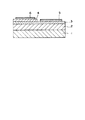
次に、本発明の実施例について添付の図面を参照して具体的に説明する。図2は本発明の第1の実施例に係るダイヤモンド薄膜ダイオードを示す断面図である。シリコンウエハ1の上に、絶縁性のダイヤモンド薄膜2が下地基板として形成されており、このダイヤモンド薄膜2の上に、ボロンドープのp型ダイヤモンド薄膜3が形成されている。そして、このp型ダイヤモンド薄膜3の上に絶縁性のアンドープダイヤモンド薄膜4が選択的に形成されていると共に、この絶縁性ダイヤモンド薄膜4の上にはAu電極6が、またp型ダイヤモンド薄膜3の上の絶縁性ダイヤモンド薄膜4に被覆されていない部分にはAu/Ti積層構造のオーミック電極5が形成されている。絶縁性ダイヤモンド薄膜2,4及びp型ダイヤモンド薄膜3は高配向性ダイヤモンド薄膜で形成されている。
【0022】
次に、上述の構造を有する本実施例の整流素子の特性を比較例と比較して説明する。先ず、この整流素子の製造工程について図2を参照して説明する。
(ステップ1)
高配向性ダイヤモンド薄膜を形成する基板として直径1インチ、方位(100)のシリコンウエハ1(n型、比抵抗1000Ω・cm以上)を用いた。この基板をマイクロ波プラズマ化学気相蒸着装置に入れ、メタン;2.5%、水素;97.5%、ガス圧;25Torr、ガス流量;300cc/分、基板温度;750℃で15分間処理した。マイクロ波入力パワーはほぼ1100Wであったが、基板温度を750℃に維持するように微調整した。これと同時に基板に負バイアス電圧を印加した。負バイアスによる電流量は12mA/cm2であった。
【0023】
(ステップ2)
その後、メタン;0.5%、水素;99.4%、酸素:0.1%、ガス圧:30Torr、ガス流量;300cc/分、基板温度;800℃で30時間合成を続けた。その結果、膜厚が約8μmで高配向したダイヤモンド薄膜2を合成することができた。電子顕微鏡観察から、この膜表面の88%が(100)結晶面で覆われていることが分かった。また、この薄膜の断面写真から各結晶面の高低差は0.2μm以下であった。
【0024】
更に、この薄膜表面の法線方向から±10°の角度で2枚の電子顕微鏡写真を撮影し、各(100)結晶面の傾きを測定したところ、隣接する結晶面の傾きの差は|△α|≦5°、|△β|≦5°、|△γ|≦5°であった。
【0025】
(ステップ3)
(ステップ1)の条件を下記表1に示すように種々変更して同様の実験を繰り返した。但し、表1の試料1は上記ステップ1の条件である。
【0026】
【表1】

試料2においては、薄膜表面の82%が(100)結晶面で覆われ、18%は面間の間隙であった。隣接するいずれの結晶面についても|△α|≦5°、|△β|≦5°、|△γ|≦5°が成り立った。
【0028】
これに対し、試料3,4では夫々薄膜表面の77%、70%が(100)結晶面で覆われ、また、隣接するいずれか少なくとも1つの結晶面で|△α|>5°、|△β|>5°又は|△γ|>5°となった。
【0029】
(ステップ4)
作製した試料1〜4の絶縁性ダイヤモンド薄膜2を下地基板として用い、以下同じプロセスにより、ダイヤモンド薄膜整流素子を作製した。即ち、この絶縁性ダイヤモンド薄膜2上に半導体層となるボロンドープp型ダイヤモンド薄膜3を5μm積層した。このときの合成条件は、メタン濃度:0.5%、水素:99.5%、ジボラン:1.0ppm、ガス圧力:35Torr、基板温度は800℃であった。
【0030】
(ステップ5)
次に、選択成長用の酸化シリコン膜をマスクとして、0.5μmの絶縁性のアンドープダイヤモンド薄膜4をBドープダイヤモンド薄膜3上に選択的に積層した。この絶縁性ダイヤモンド薄膜4の合成条件は、ジボランを添加しないこと以外は半導体ダイヤモンド薄膜3の成膜条件と同じである。
【0031】
(ステップ6)
次いで、選択成長に用いた酸化シリコンを取り除いた後、絶縁性ダイヤモンド薄膜4の電気的特性を安定化させるために、真空中で850℃、30分間熱処理を行った。その後、再びクロム酸洗浄、王水洗浄及びRCA洗浄を行った。
【0032】
(ステップ7)
その後、ボロンドープp型半導体ダイヤモンド薄膜3上にスパッタリング法によりAu/Ti積層構造を持つオーミック電極5を形成すると共に、アンドープ絶縁性ダイヤモンド薄膜4上には電子ビーム蒸着法により直径200μmのAu電極6を形成した。これにより、1インチのシリコン基板上に20個のダイヤモンド薄膜整流素子を一括して作製した。
【0033】
図3は試料1の条件で作製した整流素子の電気的特性を示す。この図3に示すように、逆方向の耐電圧が550V、順方向の電流密度(5V印加時)が300A/cm2と、優れた整流特性が得られた。この良好な整流特性は、600℃においても観察された。
【0034】
図4は表1の各条件で作製されたダイヤモンド薄膜整流素子の逆方向耐電圧を示す。この図4に示すように、本発明の実施例の試料1、2は良好な整流特性を示し、試料3、4は整流特性が悪い。このため、良好な整流特性を得るためには、本発明にて規定した配向条件が必要であることがわかる。
【0035】
次に、図5を参照して本発明の第2の実施例について説明する。シリコンウエハ7の上にBドープのp型ダイヤモンド薄膜8が形成されており、このp型ダイヤモンド薄膜8の上に絶縁性ダイヤモンド薄膜9が形成されている。そして、この絶縁性ダイヤモンド薄膜9の上にはAu電極10が選択的に形成されていると共に、シリコンウエハ7の裏面には耐熱性銀ペーストを塗布してオーミック電極11が形成されている。本実施例においては、p型ダイヤモンド薄膜8及び絶縁性ダイヤモンド薄膜9が高配向性ダイヤモンド薄膜により形成されている。
【0036】
次に、上述の構造を有する本実施例の整流素子の特性を比較例と比較して説明する。先ず、この整流素子の製造工程について図5を参照して説明する。
【0037】
(ステップ1)
高配向性ダイヤモンド薄膜を形成する基板として直径1インチ、方位(100)のシリコンウエハ7(抵抗率:0.1Ωcm以下)を用いた。基板をマイクロ波プラズマ化学気相蒸着装置に入れ、メタン:2.5%、水素:97.5%、ジボラン:1.0ppm、ガス圧:25Torr、ガス流量300cc/分、基板温度750℃で15分間処理した。マイクロ波入力パワーはほぼ1100Wであったが、基板温度を750℃に維持するように微調整した。これと同時に基板に負バイアス電圧を印加した。負バイアスによる電流量は12mA/cm2であった。
【0038】
(ステップ2)
その後、メタン:0.5%、水素:99.5%、ジボラン:1.0ppm、ガス圧:30Torr、ガス流量300cc/分、基板温度800℃で10時間合成を行った。この結果、膜厚が約3μmで高配向したBドープp型ダイヤモンド薄膜8を合成できた。電子顕微鏡観察からこの膜表面の86%が(100)結晶面で覆われていることが分かった。また、膜厚の断面写真から各結晶面の高低差は0.2μm以下であった。
【0039】
更に、この薄膜表面の法線方向から±10°の角度で2枚の電子顕微鏡写真を撮影し、各(100)結晶面の傾きを測定したところ、隣接する結晶面の傾きの差は|△α|≦5°、|△β|≦5°、|△γ|≦5°であった。
【0040】
(ステップ3)
次に、p型ダイヤモンド薄膜8上に、絶縁性のダイヤモンド薄膜9を0.5μmの厚さで積層した。合成条件は、メタン:0.5%、水素:99.4%、酸素:0.1%、ガス圧:30Torr、ガス流量300cc/分、基板温度800℃である。
【0041】
(ステップ4)
絶縁性ダイヤモンド薄膜9の電気的特性を安定化させるために、850℃に30分間真空中で加熱して熱処理を行い、その後、クロム酸、王水及びRCA洗浄を行った。
【0042】
(ステップ5)
最後に、電子ビーム蒸着装置により直径200μmのAu電極10を絶縁性ダイヤモンド薄膜9上に形成し、低抵抗シリコン基板7の裏面には、耐熱性銀ペーストを用いてオーミック電極11を形成した。
【0043】
図6は得られたダイヤモンド薄膜整流素子の電気的特性を示す。この図6に示すように、下地絶縁性ダイヤモンド薄膜2(図2参照)を使用せず、直接導電性基板上に高配向した半導体ダイヤモンド薄膜8を形成した場合にも良好な整流特性が得られることが分かる。
【0044】
なお、本発明は上記実施例に限定されるものではない。高配向性ダイヤモンド薄膜は、少なくとも半導体層として形成すれば良く、必ずしも、絶縁性ダイヤモンド薄膜4,9及び下地絶縁性ダイヤモンド薄膜2も高配向性ダイヤモンド薄膜で形成する必要はない。また、本発明のダイヤモンド整流素子の高配向性ダイヤモンド薄膜は気相合成する際に使用した基板を除去した自立性のものとすることができる。
【0045】
【発明の効果】
以上説明したように、本発明は高配向ダイヤモンド薄膜を下地絶縁性ダイヤモンド層、半導体ダイヤモンド層又は金属電極と半導体層の間の絶縁性ダイヤモンド層として形成するので、高温、ハイパワー及び高周波用整流素子として利用可能な電気的特性が優れたダイヤモンド薄膜整流素子を一括して大量に低コストで製造することができる。
【図面の簡単な説明】
【図1】高配向性ダイヤモンド薄膜の表面とオイラー角との関係を示す模式図であり、(a)は結晶面の基準配向を示し、(b)は(100)結晶面が高度に配向したダイヤモンド薄膜の表面形態を示す。
【図2】本発明の第1の実施例に係るダイヤモンド整流素子を示す断面図である。
【図3】本実施例の整流素子のダイオード特性を示すグラフ図である。
【図4】各配向条件で作成したダイヤモンド整流素子の逆方向耐電圧を示すグラフ図である。
【図5】本発明の第2の実施例に係るダイヤモンド整流素子を示す断面図である。
【図6】本実施例の整流素子のダイオード特性を示すグラフ図である。
【符号の説明】
1,7;シリコンウエハ
2,4,9;絶縁性ダイヤモンド薄膜
3,8;p型ダイヤモンド薄膜
5;Au/Tiオーミック電極
6,10;Au電極
11;銀ペーストオーミック電極[0001]
[Industrial application fields]
The present invention relates to a diamond rectifying element provided with a pair of electrodes on one surface side of a semiconductor layer made of a diamond thin film or sandwiching the semiconductor layer, and particularly suitable for use at high temperatures. About.
[0002]
[Prior art]
Diamond has a large band gap (5.5 eV), high thermal conductivity (20 W · K / cm) and high saturated carrier mobility (electrons: 2000 cm 2 / V · sec, holes: 2100 cm 2 / V · Second) and an excellent dielectric breakdown field strength (10 7 V / cm). In addition, since diamond thin films can be made into semiconductors by adding appropriate impurities, they are expected to be applied to environment-resistant electronic devices, high-power devices, high-frequency devices, etc. that operate at high temperatures and under radiation. Further, various structures and manufacturing methods have been proposed for rectifying elements using diamond thin films (Japanese Patent Laid-Open Nos. 3-120865, 3-278474, 4-26161, and 3-278463). And JP-A-1-244399, FP1589, USP5,086,014).
[0003]
[Problems to be solved by the invention]
However, these conventional diamond rectifier elements are composed of a single crystal diamond substrate, a homoepitaxial diamond thin film provided on the single crystal diamond substrate, or a polycrystalline diamond thin film. In this case, when single crystal diamond is used as a constituent element of the rectifying element, there is a practical problem that a large number of rectifying elements cannot be manufactured at a time because the substrate area is small (several mm square). In addition, the single crystal diamond substrate is extremely expensive, and there is a drawback that the manufacturing cost of the rectifying element is high. In addition, because there are many crystal defects in natural and high-pressure synthetic single crystal diamond, the electrical characteristics of the fabricated rectifier element do not reach the theoretically expected characteristics of single crystal diamond. .
[0004]
Recent progress in diamond thin film synthesis technology has made it possible to synthesize a uniform polycrystalline diamond thin film on a cheap non-diamond substrate having a diameter of about 4 inches with good reproducibility. When a rectifying element is manufactured using a polycrystalline diamond thin film, a large number of rectifying elements can be manufactured at a time, which is advantageous in that the manufacturing cost is low. However, the currently obtained polycrystalline diamond thin film has a large number of grain boundaries and crystal defects, and surface irregularities are severe. Since the grain boundary causes carrier scattering, the mobility of the carrier is greatly reduced, and an extra leakage current path is formed, thereby deteriorating the characteristics of the device. Further, when the device is operated at high temperature and in the atmosphere, the diamond thin film is oxidized and graphitized from the grain boundary portion, and the maximum use temperature of the rectifying device is lower than that in the case of a single crystal. In addition, defects existing in the crystal are a major cause of leakage current in the reverse direction as a deep level. Furthermore, local concentration of the electric field strength occurs due to the unevenness of the surface, so that local electrical breakdown occurs, resulting in large variations in characteristics between elements.
[0005]
As described above, when a rectifying element is manufactured using a polycrystalline diamond thin film, there is an advantage from the viewpoint of productivity, but the level of practical use is not reached due to the characteristics of the element.
[0006]
The present invention has been made in view of such problems, and an object of the present invention is to provide a low-cost diamond rectifying element that has excellent electrical characteristics and can be mass-produced.
[0007]
[Means for Solving the Problems]
A diamond rectifying device according to the present invention includes a semiconductor layer made of a diamond thin film formed by vapor phase synthesis, and a pair of electrodes provided on one surface side of the semiconductor layer or sandwiching the semiconductor layer. In the diamond rectifying element, the diamond thin film is a polycrystalline film, and 80% or more of the surface area of the thin film is composed of either a (100) crystal plane or a (111) crystal plane of diamond, and is adjacent (100 ) The difference of Euler angles {α, β, γ} representing each crystal plane orientation {Δα, Δβ, Δγ} for the crystal plane or (111) crystal plane is | Δα | ≦ 5 °, | Δβ It is a highly oriented film that simultaneously satisfies | ≦ 5 ° and | Δγ | ≦ 5 °.
[0008]
FIG. 1 schematically shows the structure of a diamond thin film surface in which (100) crystal planes according to the present invention are highly oriented. An X axis and a Y axis perpendicular to each other are defined in the thin film plane, and a normal direction of the thin film surface is defined as a Z axis. i-th and j-th diamond crystal faces of the crystal plane orientation Euler angles each representing a adjacent thereto {α i, β i, γ i}, {α j, β j, γ j} and the angle difference between the two Let {Δα, Δβ, Δγ}.
[0009]
Euler angles {α, β, γ} represent the orientation of crystal planes obtained by rotating the reference crystal plane around the Z, Y, and Z axes of the reference coordinates in the order of angles α, β, γ.
[0010]
In the present invention, a highly oriented diamond thin film that satisfies | Δα | ≦ 5 °, | Δβ | ≦ 5 °, and | Δγ | ≦ 5 ° at the same time. Similar to the film, the carrier mobility is high.
[0011]
Similarly, regarding the (111) crystal plane, when the absolute value of the Euler angle difference is 5 ° or less, the crystal is highly oriented and the carrier mobility is increased. Such a highly oriented diamond thin film can be formed, for example, by mirror-polishing a silicon substrate and then irradiating the substrate with a microwave while applying a negative bias to the substrate in a gas phase containing methane gas.
[0012]
[Action]
The oriented diamond thin film used in the present invention has an in-plane misorientation within ± 5 °, so that adjacent (100) planes are fused at the growth stage, and a conventional polycrystalline diamond thin film is obtained. Compared with, the influence of grain boundaries can be ignored. Moreover, since the diamond thin film is produced by vapor phase synthesis, the absolute amount of impurities and defects is less than that of natural and high-pressure synthetic single crystal diamond. This allows highly oriented diamond thin films to achieve higher hole mobility than reported for conventional polycrystalline diamond thin films and single crystal diamonds, while significantly reducing leakage currents at grain boundaries. Can be made. In addition, since the highly oriented diamond thin film has almost no grain boundary portion, oxidation and graphitization as observed in the polycrystalline diamond thin film does not occur even in the atmosphere and under high temperature, and the diamond rectifying element of the present invention has a high temperature. Under long time, stable operation is possible.
[0013]
In addition, the surface of the highly oriented diamond thin film has no irregularities, and the electric field strength and distribution generated at the interface between the electrode and the diamond thin film can be made uniform, thereby reducing variations between elements and increasing reliability. be able to. In addition, a commercially available inexpensive silicon substrate can be used as the substrate, and an alignment film can be grown on a 4-inch diameter substrate, so that mass production of diamond rectifier elements and cost reduction are possible. .
[0014]
According to a third aspect of the present invention, a high-resistance diamond layer having a thickness of 10 angstroms to 1 mm and a specific resistance of 10 2 Ωcm or more is provided between the electrode and the semiconductor layer made of a highly oriented diamond thin film. preferable. As a result, the high resistance diamond layer serves as a barrier and prevents current from flowing in both directions. When the thickness of the high resistance diamond layer is less than 10 angstroms, the carrier wave functions overlap and cause tunneling, thereby eliminating the barrier effect. For this reason, current flows in both directions, and rectification characteristics cannot be obtained. If the high-resistance diamond layer is thicker than 1 mm, the layer becomes thicker than the carrier diffusion length, and forward current does not flow. For this reason, the thickness of the high resistance diamond layer is set to 10 angstroms to 1 mm.
[0015]
On the other hand, when a diamond layer with a specific resistance of less than 10 2 Ω · cm is used as a barrier, the leakage current flowing through the high resistance diamond layer cannot be ignored when a reverse bias is applied, and good rectification characteristics can be obtained. Disappear. For this reason, the specific resistance of the high resistance diamond layer is set to 10 2 Ω · cm or more.
[0016]
The diamond thin film rectifying element according to
[0017]
Since the diamond rectifier of the present invention is chemically stable and strong against radiation, it can also be used as an environment-resistant rectifier used in a poor environment.
[0018]
Further, by monitoring the temperature change of the forward or reverse current in the rectifying element, the rectifying element of the present invention can be used as a thermistor.
[0019]
The electrode area of the diamond thin film rectifying element of the present invention can be formed in any size according to the application. Further, as specified in
[0020]
In addition, the heat resistance of the device can be improved by coating a highly oriented diamond thin film with a protective film, and a diode logic circuit can be constructed by integrating the diodes obtained in the present invention.
[0021]
【Example】
Next, embodiments of the present invention will be described in detail with reference to the accompanying drawings. FIG. 2 is a sectional view showing a diamond thin film diode according to the first embodiment of the present invention. An insulating diamond
[0022]
Next, the characteristics of the rectifying element of this embodiment having the above-described structure will be described in comparison with a comparative example. First, the manufacturing process of this rectifier will be described with reference to FIG.
(Step 1)
A silicon wafer 1 (n-type, specific resistance of 1000 Ω · cm or more) having a diameter of 1 inch and an orientation (100) was used as a substrate for forming a highly oriented diamond thin film. This substrate was placed in a microwave plasma chemical vapor deposition apparatus and treated with methane; 2.5%, hydrogen; 97.5%, gas pressure; 25 Torr, gas flow rate; 300 cc / min, substrate temperature; . The microwave input power was approximately 1100 W, but was finely adjusted to maintain the substrate temperature at 750 ° C. At the same time, a negative bias voltage was applied to the substrate. The amount of current due to the negative bias was 12 mA / cm 2 .
[0023]
(Step 2)
Thereafter, synthesis was continued at methane; 0.5%, hydrogen; 99.4%, oxygen: 0.1%, gas pressure: 30 Torr, gas flow rate: 300 cc / min, substrate temperature; 800 ° C. for 30 hours. As a result, a highly oriented diamond
[0024]
Further, two electron micrographs were taken at an angle of ± 10 ° from the normal direction of the thin film surface, and the inclination of each (100) crystal plane was measured. α | ≦ 5 °, | Δβ | ≦ 5 °, | Δγ | ≦ 5 ° .
[0025]
(Step 3)
The same experiment was repeated with various changes in the conditions of (Step 1) as shown in Table 1 below. However,
[0026]
[Table 1]
In
[0028]
On the other hand, in
[0029]
(Step 4)
Using the produced insulating diamond
[0030]
(Step 5)
Next, an insulating undoped diamond
[0031]
(Step 6)
Next, after removing the silicon oxide used for the selective growth, a heat treatment was performed in vacuum at 850 ° C. for 30 minutes in order to stabilize the electrical characteristics of the insulating diamond
[0032]
(Step 7)
Thereafter, an
[0033]
FIG. 3 shows the electrical characteristics of the rectifying element manufactured under the conditions of
[0034]
FIG. 4 shows the reverse withstand voltage of the diamond thin film rectifying element manufactured under the conditions shown in Table 1. As shown in FIG. 4,
[0035]
Next, a second embodiment of the present invention will be described with reference to FIG. A B-doped p-type diamond
[0036]
Next, the characteristics of the rectifying element of this embodiment having the above-described structure will be described in comparison with a comparative example. First, the manufacturing process of this rectifier will be described with reference to FIG.
[0037]
(Step 1)
A silicon wafer 7 (resistivity: 0.1 Ωcm or less) having a diameter of 1 inch and an orientation (100) was used as a substrate on which a highly oriented diamond thin film was formed. The substrate was put into a microwave plasma chemical vapor deposition apparatus, methane: 2.5%, hydrogen: 97.5%, diborane: 1.0 ppm, gas pressure: 25 Torr,
[0038]
(Step 2)
Thereafter, synthesis was performed at methane: 0.5%, hydrogen: 99.5%, diborane: 1.0 ppm, gas pressure: 30 Torr, gas flow rate of 300 cc / min, and substrate temperature of 800 ° C. for 10 hours. As a result, a B-doped p-type diamond
[0039]
Further, two electron micrographs were taken at an angle of ± 10 ° from the normal direction of the thin film surface, and the inclination of each (100) crystal plane was measured. α | ≦ 5 °, | △ β | ≦ 5 °, | was ≦ 5 ° | △ γ.
[0040]
(Step 3)
Next, an insulating diamond thin film 9 was laminated on the p-type diamond
[0041]
(Step 4)
In order to stabilize the electrical characteristics of the insulating diamond thin film 9, heat treatment was performed by heating in vacuum at 850 ° C. for 30 minutes, followed by chromic acid, aqua regia and RCA cleaning.
[0042]
(Step 5)
Finally, an
[0043]
FIG. 6 shows the electrical characteristics of the obtained diamond thin film rectifier. As shown in FIG. 6, good rectification characteristics can be obtained even when the semiconductor diamond
[0044]
In addition, this invention is not limited to the said Example. The highly oriented diamond thin film may be formed as at least a semiconductor layer, and the insulating diamond
[0045]
【The invention's effect】
As described above, the present invention forms a highly oriented diamond thin film as a base insulating diamond layer, a semiconductor diamond layer, or an insulating diamond layer between a metal electrode and a semiconductor layer, so that a rectifier for high temperature, high power and high frequency is used. The diamond thin film rectifying element having excellent electrical characteristics that can be used as a large number can be manufactured in a large amount at a low cost.
[Brief description of the drawings]
FIG. 1 is a schematic diagram showing the relationship between the surface of a highly oriented diamond thin film and the Euler angle, where (a) shows the reference orientation of the crystal plane, and (b) shows a highly oriented (100) crystal plane. The surface form of a diamond thin film is shown.
FIG. 2 is a cross-sectional view showing a diamond rectifier according to a first embodiment of the present invention.
FIG. 3 is a graph showing the diode characteristics of the rectifying element of this example.
FIG. 4 is a graph showing a reverse withstand voltage of a diamond rectifying element created under each orientation condition.
FIG. 5 is a cross-sectional view showing a diamond rectifier according to a second embodiment of the present invention.
FIG. 6 is a graph showing the diode characteristics of the rectifying element of this example.
[Explanation of symbols]
1, 7;
Claims (6)
Applications Claiming Priority (2)
| Application Number | Priority Date | Filing Date | Title |
|---|---|---|---|
| US6185693A | 1993-05-14 | 1993-05-14 | |
| US08/061,856 | 1993-05-14 |
Publications (2)
| Publication Number | Publication Date |
|---|---|
| JPH0750424A JPH0750424A (en) | 1995-02-21 |
| JP3755904B2 true JP3755904B2 (en) | 2006-03-15 |
Family
ID=22038582
Family Applications (1)
| Application Number | Title | Priority Date | Filing Date |
|---|---|---|---|
| JP31558693A Expired - Lifetime JP3755904B2 (en) | 1993-05-14 | 1993-12-15 | Diamond rectifier |
Country Status (2)
| Country | Link |
|---|---|
| US (1) | US5493131A (en) |
| JP (1) | JP3755904B2 (en) |
Families Citing this family (13)
| Publication number | Priority date | Publication date | Assignee | Title |
|---|---|---|---|---|
| GB9309346D0 (en) * | 1993-05-06 | 1993-06-16 | Kobe Steel Europ Ltd | Preparation of nucleated silicon surfaces |
| JPH07161455A (en) * | 1993-12-09 | 1995-06-23 | Sumitomo Electric Ind Ltd | Diamond heater |
| US5874775A (en) * | 1994-08-03 | 1999-02-23 | Sumitomo Electric Industries, Ltd. | Diamond heat sink including microchannel therein and methods for manufacturing diamond heat sinks |
| GB2300425A (en) * | 1995-05-01 | 1996-11-06 | Kobe Steel Europ Ltd | Nucleation of diamond films using an electrode |
| US5656827A (en) * | 1995-05-30 | 1997-08-12 | Vanderbilt University | Chemical sensor utilizing a chemically sensitive electrode in combination with thin diamond layers |
| JP4123496B2 (en) * | 2004-11-25 | 2008-07-23 | 独立行政法人物質・材料研究機構 | Diamond ultraviolet light sensor |
| EP2816588B1 (en) * | 2005-06-20 | 2016-09-21 | Nippon Telegraph And Telephone Corporation | Process for producing a diamond semiconductor element |
| JP5019305B2 (en) * | 2005-08-29 | 2012-09-05 | 独立行政法人物質・材料研究機構 | Diamond UV sensor |
| WO2011010654A1 (en) * | 2009-07-22 | 2011-01-27 | 独立行政法人産業技術総合研究所 | Ohmic electrode for diamond semiconductor device |
| CN108321262B (en) * | 2018-03-06 | 2024-07-26 | 西安交通大学 | A vertical structure p-diamond/i-SiC/n-diamond LED and its manufacturing method |
| CN108321271B (en) * | 2018-03-06 | 2024-07-26 | 西安交通大学 | A quasi-vertical structure p-diamond/i-SiC/n-diamond LED and its manufacturing method |
| CN110600366B (en) * | 2019-09-20 | 2021-06-18 | 西安交通大学 | (100) Crystalline diamond n-channel junction field effect transistor and method for making the same |
| CN110600554B (en) * | 2019-09-20 | 2021-06-04 | 西安交通大学 | (100) crystal orientation diamond n-i-p junction diode and preparation method thereof |
Family Cites Families (36)
| Publication number | Priority date | Publication date | Assignee | Title |
|---|---|---|---|---|
| JPS5927754A (en) * | 1982-08-04 | 1984-02-14 | Nippon Steel Corp | Nozzle for producing light-gage amorphous alloy strip |
| JPS59137396A (en) * | 1983-01-25 | 1984-08-07 | Natl Inst For Res In Inorg Mater | Synthetic method of p type semiconductor diamond |
| JPS6012747A (en) * | 1983-07-01 | 1985-01-23 | Sumitomo Electric Ind Ltd | Heat sink for electronic device |
| JPS613320A (en) * | 1984-06-18 | 1986-01-09 | Ricoh Co Ltd | Magnetic recording medium |
| JP2597976B2 (en) * | 1985-03-27 | 1997-04-09 | 株式会社東芝 | Semiconductor device and manufacturing method thereof |
| JPS61251158A (en) * | 1985-04-30 | 1986-11-08 | Sumitomo Electric Ind Ltd | heat dissipation board |
| DE3784612T2 (en) * | 1986-09-26 | 1993-09-02 | Sumitomo Electric Industries | THERMISTOR AND METHOD FOR THE PRODUCTION THEREOF. |
| JP2519740B2 (en) * | 1987-08-26 | 1996-07-31 | 住友電気工業株式会社 | Heterojunction transistor and manufacturing method thereof |
| JP2614868B2 (en) * | 1987-09-09 | 1997-05-28 | 導電性無機化合物技術研究組合 | Manufacturing method of field effect transistor |
| JP2590161B2 (en) * | 1987-12-15 | 1997-03-12 | 導電性無機化合物技術研究組合 | Manufacturing method of MIS type field effect transistor |
| JPH0823600B2 (en) * | 1988-03-25 | 1996-03-06 | 日本原子力研究所 | Remotely driven neutron irradiation capsule and remote control method for neutron irradiation |
| JPH02273960A (en) * | 1989-04-14 | 1990-11-08 | Sumitomo Electric Ind Ltd | Diamond heat sink |
| JPH0312966A (en) * | 1989-06-05 | 1991-01-21 | De Beers Ind Diamond Div Ltd | Field-effect type transistor and manufacture |
| US5089802A (en) * | 1989-08-28 | 1992-02-18 | Semiconductor Energy Laboratory Co., Ltd. | Diamond thermistor and manufacturing method for the same |
| JP2514721B2 (en) * | 1989-09-06 | 1996-07-10 | 住友電気工業株式会社 | MES type field effect transistor |
| JP2799744B2 (en) * | 1989-09-11 | 1998-09-21 | 株式会社半導体エネルギー研究所 | Manufacturing method of thermistor using diamond |
| JPH03105974A (en) * | 1989-09-19 | 1991-05-02 | Kobe Steel Ltd | Manufacture of schottky diode by synthesizing polycrystalline diamond thin film |
| JPH03110866A (en) * | 1989-09-26 | 1991-05-10 | Fujitsu Ltd | semiconductor equipment |
| JP2775903B2 (en) * | 1989-10-04 | 1998-07-16 | 住友電気工業株式会社 | Diamond semiconductor element |
| JPH03131003A (en) * | 1989-10-16 | 1991-06-04 | Kobe Steel Ltd | Diamond thin-film thermistor |
| JP2519328B2 (en) * | 1989-11-18 | 1996-07-31 | 株式会社東芝 | Semiconductor device and manufacturing method thereof |
| JP2730271B2 (en) * | 1990-03-07 | 1998-03-25 | 住友電気工業株式会社 | Semiconductor device |
| JP2813023B2 (en) * | 1990-03-13 | 1998-10-22 | 株式会社神戸製鋼所 | MIS type diamond field effect transistor |
| US5126206A (en) * | 1990-03-20 | 1992-06-30 | Diamonex, Incorporated | Diamond-on-a-substrate for electronic applications |
| JPH03278463A (en) * | 1990-03-27 | 1991-12-10 | Canon Inc | Method of forming schottky diode |
| JP2913765B2 (en) * | 1990-05-21 | 1999-06-28 | 住友電気工業株式会社 | Method of forming shot key junction |
| JP2884707B2 (en) * | 1990-05-21 | 1999-04-19 | 住友電気工業株式会社 | Hall element |
| US5124179A (en) * | 1990-09-13 | 1992-06-23 | Diamonex, Incorporated | Interrupted method for producing multilayered polycrystalline diamond films |
| US5173761A (en) * | 1991-01-28 | 1992-12-22 | Kobe Steel Usa Inc., Electronic Materials Center | Semiconducting polycrystalline diamond electronic devices employing an insulating diamond layer |
| JPH07118546B2 (en) * | 1991-03-22 | 1995-12-18 | 株式会社神戸製鋼所 | Diamond heterojunction diode |
| JPH0815160B2 (en) * | 1991-03-29 | 1996-02-14 | 株式会社神戸製鋼所 | Diamond Schottky gate type field effect transistor |
| US5199918A (en) * | 1991-11-07 | 1993-04-06 | Microelectronics And Computer Technology Corporation | Method of forming field emitter device with diamond emission tips |
| US5397428A (en) * | 1991-12-20 | 1995-03-14 | The University Of North Carolina At Chapel Hill | Nucleation enhancement for chemical vapor deposition of diamond |
| US5391895A (en) * | 1992-09-21 | 1995-02-21 | Kobe Steel Usa, Inc. | Double diamond mesa vertical field effect transistor |
| JPH0794805A (en) * | 1993-05-14 | 1995-04-07 | Kobe Steel Ltd | Highly-oriented diamond thin-film magnetic sensing element, and magnetic sensor |
| US5371383A (en) * | 1993-05-14 | 1994-12-06 | Kobe Steel Usa Inc. | Highly oriented diamond film field-effect transistor |
-
1993
- 1993-12-15 JP JP31558693A patent/JP3755904B2/en not_active Expired - Lifetime
-
1994
- 1994-09-28 US US08/314,548 patent/US5493131A/en not_active Expired - Lifetime
Also Published As
| Publication number | Publication date |
|---|---|
| US5493131A (en) | 1996-02-20 |
| JPH0750424A (en) | 1995-02-21 |
Similar Documents
| Publication | Publication Date | Title |
|---|---|---|
| JP3380313B2 (en) | Diamond field effect transistor | |
| CN102163627B (en) | Sic semiconductor device having schottky barrier diode and method for manufacturing the same | |
| JP3755904B2 (en) | Diamond rectifier | |
| Wittmer et al. | Electrical characteristics of TiN contacts to N silicon | |
| CN104867969B (en) | Diode apparatus | |
| JP3930561B2 (en) | Ohmic contact and method for manufacturing a semiconductor device comprising such an ohmic contact | |
| EP0789388B1 (en) | Fabrication method for schottky electrodes onto semiconductor devices | |
| US5512873A (en) | Highly-oriented diamond film thermistor | |
| Sun et al. | P-Type conductivity of hexagonal boron nitride as a dielectrically tunable monolayer: Modulation doping with magnesium | |
| JP2019016680A (en) | Schottky barrier diode | |
| US5442199A (en) | Diamond hetero-junction rectifying element | |
| US5309000A (en) | Diamond films with heat-resisting ohmic electrodes | |
| TWI286773B (en) | Field emission type electron source | |
| JP3587224B2 (en) | Ohmic electrode | |
| JPH07161455A (en) | Diamond heater | |
| JPH0786311A (en) | Highly oriented diamond thin film field effect transistor | |
| JP3934822B2 (en) | Schottky diode and manufacturing method thereof | |
| JP2911122B2 (en) | Method for forming ohmic electrode of silicon carbide semiconductor device | |
| JP4645641B2 (en) | Method for manufacturing SiC Schottky diode | |
| JPS6248390B2 (en) | ||
| JP3924628B2 (en) | Method for manufacturing SiC Schottky diode | |
| JPH08316498A (en) | Diamond semiconductor rectifying element | |
| TWI246204B (en) | Electrode for p-type SiC | |
| JPH05283361A (en) | Diamond semiconductor device and manufacturing method thereof | |
| JP3525150B2 (en) | Method for manufacturing silicon carbide semiconductor substrate |
Legal Events
| Date | Code | Title | Description |
|---|---|---|---|
| A131 | Notification of reasons for refusal |
Free format text: JAPANESE INTERMEDIATE CODE: A131 Effective date: 20041012 |
|
| A521 | Request for written amendment filed |
Free format text: JAPANESE INTERMEDIATE CODE: A523 Effective date: 20041224 |
|
| A131 | Notification of reasons for refusal |
Free format text: JAPANESE INTERMEDIATE CODE: A131 Effective date: 20050125 |
|
| A521 | Request for written amendment filed |
Free format text: JAPANESE INTERMEDIATE CODE: A523 Effective date: 20050426 |
|
| A521 | Request for written amendment filed |
Free format text: JAPANESE INTERMEDIATE CODE: A821 Effective date: 20050427 |
|
| A072 | Dismissal of procedure [no reply to invitation to correct request for examination] |
Free format text: JAPANESE INTERMEDIATE CODE: A072 Effective date: 20050705 |
|
| A02 | Decision of refusal |
Free format text: JAPANESE INTERMEDIATE CODE: A02 Effective date: 20050913 |
|
| A521 | Request for written amendment filed |
Free format text: JAPANESE INTERMEDIATE CODE: A523 Effective date: 20050915 |
|
| A911 | Transfer to examiner for re-examination before appeal (zenchi) |
Free format text: JAPANESE INTERMEDIATE CODE: A911 Effective date: 20051027 |
|
| TRDD | Decision of grant or rejection written | ||
| A01 | Written decision to grant a patent or to grant a registration (utility model) |
Free format text: JAPANESE INTERMEDIATE CODE: A01 Effective date: 20051220 |
|
| A61 | First payment of annual fees (during grant procedure) |
Free format text: JAPANESE INTERMEDIATE CODE: A61 Effective date: 20051220 |
|
| R150 | Certificate of patent or registration of utility model |
Free format text: JAPANESE INTERMEDIATE CODE: R150 |
|
| FPAY | Renewal fee payment (event date is renewal date of database) |
Free format text: PAYMENT UNTIL: 20100106 Year of fee payment: 4 |
|
| FPAY | Renewal fee payment (event date is renewal date of database) |
Free format text: PAYMENT UNTIL: 20110106 Year of fee payment: 5 |
|
| FPAY | Renewal fee payment (event date is renewal date of database) |
Free format text: PAYMENT UNTIL: 20120106 Year of fee payment: 6 |
|
| FPAY | Renewal fee payment (event date is renewal date of database) |
Free format text: PAYMENT UNTIL: 20130106 Year of fee payment: 7 |
|
| FPAY | Renewal fee payment (event date is renewal date of database) |
Free format text: PAYMENT UNTIL: 20130106 Year of fee payment: 7 |
|
| EXPY | Cancellation because of completion of term |