JP3742442B2 - Display control method and circuit for liquid crystal display panel - Google Patents
Display control method and circuit for liquid crystal display panel Download PDFInfo
- Publication number
- JP3742442B2 JP3742442B2 JP11869995A JP11869995A JP3742442B2 JP 3742442 B2 JP3742442 B2 JP 3742442B2 JP 11869995 A JP11869995 A JP 11869995A JP 11869995 A JP11869995 A JP 11869995A JP 3742442 B2 JP3742442 B2 JP 3742442B2
- Authority
- JP
- Japan
- Prior art keywords
- liquid crystal
- crystal display
- display panel
- video data
- signal
- Prior art date
- Legal status (The legal status is an assumption and is not a legal conclusion. Google has not performed a legal analysis and makes no representation as to the accuracy of the status listed.)
- Expired - Fee Related
Links
Images


Classifications
-
- G—PHYSICS
- G09—EDUCATION; CRYPTOGRAPHY; DISPLAY; ADVERTISING; SEALS
- G09G—ARRANGEMENTS OR CIRCUITS FOR CONTROL OF INDICATING DEVICES USING STATIC MEANS TO PRESENT VARIABLE INFORMATION
- G09G3/00—Control arrangements or circuits, of interest only in connection with visual indicators other than cathode-ray tubes
- G09G3/20—Control arrangements or circuits, of interest only in connection with visual indicators other than cathode-ray tubes for presentation of an assembly of a number of characters, e.g. a page, by composing the assembly by combination of individual elements arranged in a matrix no fixed position being assigned to or needed to be assigned to the individual characters or partial characters
- G09G3/34—Control arrangements or circuits, of interest only in connection with visual indicators other than cathode-ray tubes for presentation of an assembly of a number of characters, e.g. a page, by composing the assembly by combination of individual elements arranged in a matrix no fixed position being assigned to or needed to be assigned to the individual characters or partial characters by control of light from an independent source
- G09G3/36—Control arrangements or circuits, of interest only in connection with visual indicators other than cathode-ray tubes for presentation of an assembly of a number of characters, e.g. a page, by composing the assembly by combination of individual elements arranged in a matrix no fixed position being assigned to or needed to be assigned to the individual characters or partial characters by control of light from an independent source using liquid crystals
- G09G3/3611—Control of matrices with row and column drivers
-
- G—PHYSICS
- G09—EDUCATION; CRYPTOGRAPHY; DISPLAY; ADVERTISING; SEALS
- G09G—ARRANGEMENTS OR CIRCUITS FOR CONTROL OF INDICATING DEVICES USING STATIC MEANS TO PRESENT VARIABLE INFORMATION
- G09G3/00—Control arrangements or circuits, of interest only in connection with visual indicators other than cathode-ray tubes
- G09G3/20—Control arrangements or circuits, of interest only in connection with visual indicators other than cathode-ray tubes for presentation of an assembly of a number of characters, e.g. a page, by composing the assembly by combination of individual elements arranged in a matrix no fixed position being assigned to or needed to be assigned to the individual characters or partial characters
- G09G3/34—Control arrangements or circuits, of interest only in connection with visual indicators other than cathode-ray tubes for presentation of an assembly of a number of characters, e.g. a page, by composing the assembly by combination of individual elements arranged in a matrix no fixed position being assigned to or needed to be assigned to the individual characters or partial characters by control of light from an independent source
- G09G3/36—Control arrangements or circuits, of interest only in connection with visual indicators other than cathode-ray tubes for presentation of an assembly of a number of characters, e.g. a page, by composing the assembly by combination of individual elements arranged in a matrix no fixed position being assigned to or needed to be assigned to the individual characters or partial characters by control of light from an independent source using liquid crystals
- G09G3/3607—Control arrangements or circuits, of interest only in connection with visual indicators other than cathode-ray tubes for presentation of an assembly of a number of characters, e.g. a page, by composing the assembly by combination of individual elements arranged in a matrix no fixed position being assigned to or needed to be assigned to the individual characters or partial characters by control of light from an independent source using liquid crystals for displaying colours or for displaying grey scales with a specific pixel layout, e.g. using sub-pixels
Landscapes
- Engineering & Computer Science (AREA)
- Chemical & Material Sciences (AREA)
- Crystallography & Structural Chemistry (AREA)
- Physics & Mathematics (AREA)
- Computer Hardware Design (AREA)
- General Physics & Mathematics (AREA)
- Theoretical Computer Science (AREA)
- Liquid Crystal Display Device Control (AREA)
- Control Of Indicators Other Than Cathode Ray Tubes (AREA)
- Liquid Crystal (AREA)
- Transforming Electric Information Into Light Information (AREA)
Description
【0001】
【産業上の利用分野】
本発明は液晶表示パネルに係り、特に液晶表示パネルの表示制御方法及びその回路に関する。
【0002】
【従来の技術】
従来のデルタ構造(delta(又は、triangle) structure)の液晶表示パネルでビデオデータを示す場合、その構造的な問題によりビデオデータが示された時に画面に凹凸部分が生じて画質が劣化する問題点があった。
【0003】
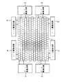
前記のような問題点が発生される従来のデルタ構造の液晶表示パネルとパネルを駆動するための駆動回路のブロック図を図1に示した。図1を参照すれば、液晶表示パネル装置はデルタ構造の液晶表示パネル1、前記液晶表示パネル1の奇数番目のラインを駆動するための奇数番目のゲート駆動回路2、前記液晶表示パネル1の偶数番目のラインを駆動するための偶数番目のゲート駆動回路3、前記液晶表示パネル1の駆動されたラインの奇数番目ピクセルにビデオデータを印加するための奇数番目のソース駆動回路4及び前記液晶表示パネル1の駆動されたラインの偶数番目ピクセルにビデオデータを印加するための偶数番目のソース駆動回路5より構成されている。
【0004】
即ち、前記液晶表示パネル1の各ピクセルはゲート駆動回路2,3とソース駆動回路4,5により駆動されることにより、ビデオデータが前記各ピクセルに印加されうる。液晶表示パネル1の横辺はソース駆動回路4,5により、縦辺はゲート駆動回路2,3により制御される。即ち、パネルの上部に位置したソース駆動回路4はパネル1の該当奇数行のピクセルを、パネルの下部に位置したソース駆動回路5はパネル1の該当偶数行のピクセルを駆動し、パネルの左側に位置したゲート駆動回路2はパネル1の該当奇数列のピクセルを、パネルの右側に位置したゲート駆動回路3はパネル1の該当偶数列のピクセルを駆動する構造よりなっている。
【0005】
デルタ構造では図1に示したようにビデオデータはソース駆動回路4,5によりジグザグ型で連結された該当ピクセル行に入力されるようになるが、デルタ構造の特性のため直四角形を示す場合、図2に示したようにその左右縁部に凹凸部分が生じるようになる。これはビデオデータの出力がソース駆動回路4,5により前記各該当ピクセル列の各ピクセルに印加される時点が同一であるからである。例えば、図2を参照すれば、右側から5,9番目のピクセル列を構成する各ピクセルがソース駆動回路54により同一な時点で駆動されれば、図2に示された直四角形の左右縁部に突出され陥没された部分が生じるようになる。
【0006】
【発明が解決しようとする課題】
したがって、本発明の目的は液晶表示パネルを駆動するソース駆動回路の動作時点をフィールドに従って偶数、或いは奇数列で変動させて表示の左右縁部から発生される突出され陥没された部分を減少させうる液晶表示パネルの表示制御方法を提供するにある。
【0007】
本発明の他の目的は前記の方法を具現した液晶表示パネルの表示制御回路を提供するにある。
【0008】
【課題を達成するための手段】
前記の目的を達成するために本発明の液晶表示パネルの表示制御方法は、デルタ構造の液晶表示パネルにデータを示すための液晶表示パネルの表示制御方法において、第1フィールド期間の間前記液晶表示パネルに元のデータを示す段階と、第2フィールド期間の間前記液晶表示パネルに元のデータの偶数番目のライン(又は奇数番目のライン)に示されるデータを1ピクセル区間移動させて示す段階よりなっている。
【0009】
前記他の目的を達成するために本発明の液晶表示パネルの表示制御回路は、デルタ構造の液晶表示パネルと、前記液晶表示パネルのソースを駆動するためのソース駆動手段と、前記液晶表示パネルのゲートを駆動するためのゲート駆動手段とを具備した液晶表示パネルの表示制御回路において、前記ソース駆動手段が第1フィールド期間の間は前記液晶表示パネルに元の映像データを示すための第1信号により制御され、第2フィールド期間の間は前記液晶表示パネルの偶数番目のライン(又は奇数番目のライン)のデータを1ピクセルの表示期間区間移動させて示すための第2信号により制御されることを特徴とする。
【0010】
【作用】
デルタ構造の液晶表示パネルの構造上、画面に現れる凹凸表示の画面を取り除くことにより、表示装置の画質を改善することができる。
【0011】
【実施例】
以下、添付した図面に基づき本発明の液晶表示パネルの表示制御方法及びその回路を詳細に説明する。
【0012】
図2に示した画面を本発明の方法により表示しようとする時、まず、図2に示された画面を1フレーム(又は1フィールド)期間の間示す。次に、二番目のフレーム(又はフィールド)で図2に示した画面の偶数番目(又は奇数番目)のラインを1ピクセル区間移動させて示す。このようにすると、図2に示した画面の突出され陥没された部分が相殺されて直線のように見えるようになる。
【0013】
図3は図2に示した直四角形の画面の偶数番目のラインを1ピクセル区間移動させて示す場合の液晶表示パネル及び駆動回路のブロック図である。
【0014】
図4は図2に示された画面と図3に示した画面の合成により人の目には殆ど突出されたり陥没されている部分がなさそうに見えることを示す画面である。
【0015】
即ち、2フィールドで1フレームをなすビデオデータ表示において、第1フィールドには図2に示したような画面を示し、第2フィールドには図3に示したように偶数番目のラインのデータを1ピクセル区間移動されるようにイネーブルさせて画面を示すと、図4に示したように見えるようになる。
【0016】
ソース駆動回路4,5を先にイネーブルさせると、ビデオデータが1ピクセル遅延されて現れるようになる。これはビデオデータは常に出力時点が一定なのでサンプリンの時点に従って現れる現象である。このような内容は後述する説明により明白になろう。図3は偶数番目のラインである時、ソース駆動回路4,5を先にイネーブルさせて示した表示画面である。もし、第1フィールドを正常的に図2のように示し、その後、第2フィールドを図3のように示すと、最終的に示される画面は図4に示した画面のように見える。
【0017】
これをより具体的に調べると次の通りである。
【0018】
図2と図3に示した画面の共通部分は濃く示され、それぞれ示される部分は相対的に薄くなって図2に示した従来の表示画面に比して突出され陥没された部分が相対的に薄くなる。これと共に、その薄く示された部分で色の干渉が発生されてジグザグ部分がさらに少なく現れることのように見える。
【0019】
前記の方法をハードウエアで具現するために所定の制御器(図示せず)でソース駆動回路4,5に印加される所定の開始信号とキャリパルス信号のみを操作すればよい。即ち、開始信号は一定にしキャリパルスのみ1ピクセルキャリオーバタイムインタバル先に発生するように構成すればよい。これを説明すれば、偶数番目のラインは右側のゲート駆動回路3が駆動するラインに偶数番目のゲート駆動回路のイネーブル区間とフィールド毎に入る垂直同期信号によりトグリングされるフィールド信号による共通区間に図3に示したように示されるようにすればよい。
【0020】
図5は奇数番目の水平ラインの開始信号とキャリパルス信号のタイミングを示す。
【0021】
図5において、ソース駆動回路4,5は奇数番目の水平ラインを駆動するための開始信号(STH1,STH2)より遅くビデオデータをピクセルに印加するようになる。即ち、水平ラインキャリパルス信号(ICPH1,ICPH2)が1ピクセル遅延されて現れるようになっている。したがって、図2,3に示された奇数番目の水平ラインのピクセルと図2に示された偶数番目の水平ラインのピクセルは5番目のピクセルからビデオデータを示すようになる。ここで、図5に記載された数字1,2,3,4は水平ラインのピクセルがイネーブルされる順序を示す。
【0022】
即ち、キャリパルスを先に発生させることによりビデオデータは1ピクセル遅延されて示される。
【0023】
図6は図3の偶数番目の水平ラインを駆動するための開始信号とキャリパルス信号のタイミングを示す。
【0024】
図6において、偶数番目の水平ラインを駆動するための開始信号(STH1,STH2)に合わせてソース駆動回路4,5がデータをピクセルに印加するようになる。即ち、水平ラインキャリパルス信号(CPH1,CPH2)が図5に示したキャリパルス信号より1ピクセルより先に現れるようになる。したがって、図3に示された偶数番目の水平ラインのピクセルは6番目のピクセルからビデオデータを示すようになる。これは6番目のピクセルより先に1番目から5番目のピクセルがキャリパルス信号(CPH1,CPH2)によりイネーブルされるようになり、ビデオデータの出力は6番目のピクセルがイネーブルされる時に印加されるからである。ここで、図5に記載された数字1,2,3,4,5は水平ラインのピクセルがイネーブルされる順序を示す。
【0025】
図7は図6に示したキャリパルス信号(CPH1,CPH2)を発生するための回路の回路図である。
【0026】
図7において、図6に示したキャリパルス信号を発生するための回路はフィールドアウト信号と垂直ラインキャリパルス信号CPV1を入力して反転論理和するNORゲート100、前記NORゲート100の出力信号を反転するインバータ110、前記図5に示したキャリパルス信号ICPH2を反転するためのインバータ120、前記インバータ110の第1状態の出力信号を選択信号として前記図5に示したキャリパルス信号(ICPH1,ICPH2)をそのまま出力したり、前記インバータ110の第2状態の出力信号を選択信号として前記インバータ120の出力信号をキャリパルス信号CPH1に出力し、図5に示したキャリパルス信号ICHP1をキャリパルス信号CPH2に出力するための第1,第2選択手段130,140より構成されている。
【0027】
図7を参照すれば、前記垂直ラインキャリパルス信号CPV1は液晶表示パネルの縦を制御するパルスとして有効ビデオデータ区間で開始して第1ラインから示されるようにする。そして、前記フィールドアウト信号が“ハイ”ならば、キャリパルス信号(ICPH1,ICPH2)がそのまま出力されるが、その次のフィールド、即ちフィールドアウト信号が“ロー”ならば、前記垂直ラインキャリパルス信号CPV1が“ハイ”である時、前記キャリパルス信号(ICPH1,ICPH2)がそのまま出力され、垂直ラインキャリパルス信号CPV1が“ロー”である時はキャリパルス信号ICPH1はキャリパルス信号CPH2にキャリパルス信号ICPH2はキャリパルス信号CPH1に転換されて出力される。したがって、フィールドアウト信号を適切に“ロー”とすれば、図6に示したキャリパルス(CPH1,CPH2)が図5に示されたキャリパルス(ICPH1,ICPH2)より1/4クロック周期先行されて発生されうる。ここで、液晶表示パネルは前記キャリパルススの1/4クロック周期ごとに横で1ピクセルずつ所定のビデオデータをディスプレイする。したがって、キャリパルス信号が1ピクセル先に発生するようになると、4ピクセルにディスプレイされるべきデータは5ピクセル部分にラッチされてディスプレイされるので偶数列はフィールドアウト信号に応じて正常的にディスプレイしていて、その次のフィールドでは偶数列に1ピクセルずつシフトしてディスプレイするようになる。
【0028】
前記選択手段130,140はS端子にハイ信号が印加されると11番端子に印加される信号がO端子を通じて出力され、S端子にロー信号が印加されれば12番端子に印加される信号がO端子を通じて出力されるように作用する。
【0029】
図8は図7に示されたフィールドアウト出力信号発生回路の回路図である。
【0030】
図8において、フィールドアウト出力信号発生回路は垂直同期信号(Vsync)に応答してトグリングされたフィールドアウト出力信号を発生するためのTフリップフロップ150より構成されている。
【0031】
図7と図8に示した回路は垂直ラインキャリパルス信号CPV1が偶数番目のラインでは“ロー”である。フィールドアウト信号が“ロー”レベルであり、垂直ラインキャリパルス信号CPV1が“ロー”レベルである時、図6に示された水平ラインキャリパルス(CPH1,CHP2)が発生するようになる。
【0032】
図7と図8に示した回路は偶数番目のラインを制御するためのものであって、奇数番目のラインを制御するための回路の構成は変更すべきである。即ち、図7に示された偶数ラインをコントロールする垂直ラインキャリパルス信号CPV1を奇数ラインをコントロールする垂直ラインキャリパルス信号CPV2(図示せず)に交替すればよい。
【0033】
【発明の効果】
したがって、請求項1から請求項6に示されている本発明の液晶表示パネルの表示制御方法及び回路によれば、デルタ構造の液晶表示パネルの構造上画面に現れる凹凸表示の画面を取り除いて表示装置の画質を改善することができる。
【図面の簡単な説明】
【図1】デルタ構造の液晶表示パネルの構造と駆動回路のブロック図である。
【図2】表示しようとする直四角形の画面を示す。
【図3】図2に示した直四角形の偶数番目のラインを1ピクセル先に示した場合に現れる画面である。
【図4】図2に示した画面と図3に示した画面とを合成した場合に現れる表示画面である。
【図5】正常的なライン表示時にスタート信号とキャリ信号とのタイミングを示す。
【図6】1ピクセル表示期間ほど区間移動させて示す場合にスタート信号とキャリ信号とのタイミングを示す。
【図7】水平ラインのキャリパルス発生回路の回路図である。
【図8】フィールド出力信号発生回路の回路図である。
【符号の説明】
2,3…ゲート駆動回路、
4,5…ソース駆動回路。[0001]
[Industrial application fields]
The present invention relates to a liquid crystal display panel, and more particularly to a display control method and circuit for a liquid crystal display panel.
[0002]
[Prior art]
When displaying video data on a conventional delta (or triangle) liquid crystal display panel, when the video data is displayed due to a structural problem, the image quality deteriorates due to irregularities on the screen. was there.
[0003]
FIG. 1 shows a block diagram of a conventional delta structure liquid crystal display panel in which the above-described problems occur and a driving circuit for driving the panel. Referring to FIG. 1, a liquid crystal display panel device includes a liquid crystal display panel 1 having a delta structure, an odd-numbered
[0004]
That is, each pixel of the liquid crystal display panel 1 is driven by the
[0005]
In the delta structure, as shown in FIG. 1, the video data is input to the corresponding pixel rows connected in a zigzag form by the
[0006]
[Problems to be solved by the invention]
Accordingly, it is an object of the present invention to reduce the protruding and depressed portions generated from the left and right edges of the display by changing the operation time of the source driving circuit for driving the liquid crystal display panel in even or odd columns according to the field. It is in providing the display control method of a liquid crystal display panel.
[0007]
Another object of the present invention is to provide a display control circuit of a liquid crystal display panel embodying the above method.
[0008]
[Means for achieving the object]
In order to achieve the above object, a display control method for a liquid crystal display panel according to the present invention is a display control method for a liquid crystal display panel for displaying data on a delta structure liquid crystal display panel. From the step of displaying the original data on the panel and the step of moving the data indicated by the even-numbered line (or odd-numbered line) of the original data to the liquid crystal display panel by moving one pixel section during the second field period. It has become.
[0009]
In order to achieve the other object, a display control circuit of a liquid crystal display panel according to the present invention comprises a delta structure liquid crystal display panel, source driving means for driving the source of the liquid crystal display panel, and the liquid crystal display panel. In a display control circuit of a liquid crystal display panel, comprising a gate driving means for driving a gate, a first signal for the source driving means to display original video data on the liquid crystal display panel during a first field period During the second field period, the data of the even-numbered line (or odd-numbered line) of the liquid crystal display panel is controlled by a second signal for moving the display period of one pixel and indicating it. It is characterized by.
[0010]
[Action]
Due to the structure of the liquid crystal display panel having the delta structure, the image quality of the display device can be improved by removing the uneven display screen that appears on the screen.
[0011]
【Example】
Hereinafter, a display control method and circuit of a liquid crystal display panel according to the present invention will be described in detail with reference to the accompanying drawings.
[0012]
When the screen shown in FIG. 2 is to be displayed by the method of the present invention, first, the screen shown in FIG. 2 is shown for one frame (or one field) period. Next, the even-numbered (or odd-numbered) line of the screen shown in FIG. 2 is moved by one pixel section in the second frame (or field). If it does in this way, the projected and depressed part of the screen shown in FIG. 2 will cancel and it will look like a straight line.
[0013]
FIG. 3 is a block diagram of the liquid crystal display panel and the driving circuit in the case where the even-numbered lines of the rectangular screen shown in FIG. 2 are moved by one pixel section .
[0014]
FIG. 4 is a screen showing that the portion shown in FIG. 2 and the screen shown in FIG. 3 are almost not projected or depressed by human eyes.
[0015]
That is, in the video data display that forms one frame by two fields, the screen as shown in FIG. 2 is shown in the first field, and the data of the even-numbered line is 1 in the second field as shown in FIG. When the screen is displayed with it enabled to be moved by a pixel interval , it appears as shown in FIG.
[0016]
When the
[0017]
A more specific examination is as follows.
[0018]
The common parts of the screens shown in FIGS. 2 and 3 are shown dark, the parts shown are relatively thin, and the projected and depressed parts of the conventional display screen shown in FIG. It becomes thinner. At the same time, color interference is generated in the thinly shown portion, and it seems that the zigzag portion appears less.
[0019]
In order to implement the above method in hardware, only a predetermined start signal and carry pulse signal applied to the
[0020]
FIG. 5 shows the timing of the start signal and carry pulse signal of the odd-numbered horizontal line.
[0021]
In FIG. 5, the
[0022]
That is, the video data is shown delayed by one pixel by generating the carry pulse first.
[0023]
FIG. 6 shows the timing of the start signal and the carry pulse signal for driving the even-numbered horizontal lines in FIG.
[0024]
In FIG. 6, the
[0025]
FIG. 7 is a circuit diagram of a circuit for generating carry pulse signals (CPH1, CPH2) shown in FIG.
[0026]
In FIG. 7, the circuit for generating the carry pulse signal shown in FIG. 6 receives the field-out signal and the vertical line carry pulse signal CPV1 and inverts the NOR
[0027]
Referring to FIG. 7, the vertical line carry pulse signal CPV1 starts from the effective video data section as a pulse for controlling the vertical direction of the liquid crystal display panel and is indicated from the first line. If the field-out signal is “high”, the carry pulse signals (ICPH1, ICPH2) are output as they are. If the next field, that is, the field-out signal is “low”, the vertical line carry pulse signal is output. When CPV1 is “high”, the carry pulse signals (ICPH1, ICPH2) are output as they are, and when the vertical line carry pulse signal CPV1 is “low”, the carry pulse signal ICPH1 is carried by the carry pulse signal CPH2. ICPH2 is converted into a carry pulse signal CPH1 and output. Therefore, if the field-out signal is appropriately set to “low”, the carry pulses (CPH1, CPH2) shown in FIG. 6 are preceded by the ¼ clock cycle from the carry pulses (ICPH1, ICPH2) shown in FIG. Can be generated. Here, the liquid crystal display panel displays predetermined video data by one pixel horizontally for every 1/4 clock cycle of the carry pulses. Therefore, when the carry pulse signal is generated one pixel ahead, the data to be displayed on the four pixels is latched and displayed on the five-pixel portion, so that the even columns are normally displayed according to the field-out signal. In the next field, display is performed by shifting one pixel at a time to even columns.
[0028]
When the high signal is applied to the S terminal, the selection means 130, 140 outputs a signal applied to the 11th terminal through the O terminal, and when a low signal is applied to the S terminal, the selection means 130, 140 is a signal applied to the 12th terminal. Is output through the O terminal.
[0029]
FIG. 8 is a circuit diagram of the field-out output signal generating circuit shown in FIG.
[0030]
In FIG. 8, the field-out output signal generation circuit includes a T flip-
[0031]
In the circuits shown in FIGS. 7 and 8, the vertical line carry pulse signal CPV1 is “low” in even-numbered lines. When the field-out signal is at the “low” level and the vertical line carry pulse signal CPV1 is at the “low” level, the horizontal line carry pulses (CPH1, CHP2) shown in FIG. 6 are generated.
[0032]
The circuits shown in FIGS. 7 and 8 are for controlling even-numbered lines, and the configuration of the circuit for controlling odd-numbered lines should be changed. That is, the vertical line carry pulse signal CPV1 for controlling the even lines shown in FIG. 7 may be replaced with the vertical line carry pulse signal CPV2 (not shown) for controlling the odd lines.
[0033]
【The invention's effect】
Therefore, according to the display control method and circuit of the liquid crystal display panel of the present invention described in claims 1 to 6, the display of the uneven display appearing on the screen on the structure of the liquid crystal display panel of the delta structure is removed and displayed. The image quality of the device can be improved.
[Brief description of the drawings]
FIG. 1 is a block diagram of a structure and a driving circuit of a liquid crystal display panel having a delta structure.
FIG. 2 shows a rectangular screen to be displayed.
FIG. 3 is a screen that appears when an even-numbered line of the rectangular shape shown in FIG. 2 is shown one pixel ahead.
4 is a display screen that appears when the screen shown in FIG. 2 and the screen shown in FIG. 3 are combined.
FIG. 5 shows the timing of a start signal and a carry signal during normal line display.
FIG. 6 shows the timing of a start signal and a carry signal when a section is moved by about one pixel display period.
FIG. 7 is a circuit diagram of a horizontal line carry pulse generation circuit;
FIG. 8 is a circuit diagram of a field output signal generation circuit.
[Explanation of symbols]
2, 3 ... gate drive circuit,
4, 5 ... Source drive circuit.
Claims (6)
第1フィールド期間の間前記液晶表示パネルに元のビデオデータを示す段階と、
第2フィールド期間の間前記液晶表示パネルに元のビデオデータの所定のラインに示されるデータを1ピクセル区間移動させて示す段階よりなることを特徴とする液晶表示パネルの表示制御方法。In a liquid crystal display panel display control method for displaying video data on a liquid crystal display panel having a delta structure,
Showing original video data on the liquid crystal display panel during a first field period;
A display control method for a liquid crystal display panel, comprising: moving the data indicated by a predetermined line of the original video data to the liquid crystal display panel by moving one pixel section during the second field period.
前記液晶表示パネルのソースを駆動するためのソース駆動手段と、
前記液晶表示パネルのゲートを駆動するためのゲート駆動手段とを具備した液晶表示パネルの表示制御回路において、
前記ソース駆動手段が第1フィールド期間の間は前記液晶表示パネルに元の映像データを示すための第1信号により制御され、第2フィールド期間の間は前記液晶表示パネルの所定のラインのデータを1ピクセルの表示期間区間移動させて示すための第2信号により制御されることを特徴とする液晶表示パネルの制御回路。A liquid crystal display panel with a delta structure;
Source driving means for driving the source of the liquid crystal display panel;
In a display control circuit of a liquid crystal display panel comprising a gate driving means for driving the gate of the liquid crystal display panel,
The source driving means is controlled by a first signal for indicating the original video data to the liquid crystal display panel during the first field period, and a predetermined line data of the liquid crystal display panel is supplied during the second field period. A control circuit for a liquid crystal display panel, wherein the control circuit is controlled by a second signal for moving the display period of one pixel for display .
Applications Claiming Priority (2)
| Application Number | Priority Date | Filing Date | Title |
|---|---|---|---|
| KR94P10775 | 1994-05-17 | ||
| KR1019940010775A KR0120574B1 (en) | 1994-05-17 | 1994-05-17 | Control method and circuit for liquid crystal panel |
Publications (2)
| Publication Number | Publication Date |
|---|---|
| JPH0850467A JPH0850467A (en) | 1996-02-20 |
| JP3742442B2 true JP3742442B2 (en) | 2006-02-01 |
Family
ID=19383253
Family Applications (1)
| Application Number | Title | Priority Date | Filing Date |
|---|---|---|---|
| JP11869995A Expired - Fee Related JP3742442B2 (en) | 1994-05-17 | 1995-05-17 | Display control method and circuit for liquid crystal display panel |
Country Status (4)
| Country | Link |
|---|---|
| US (1) | US5654777A (en) |
| JP (1) | JP3742442B2 (en) |
| KR (1) | KR0120574B1 (en) |
| TW (1) | TW488544U (en) |
Families Citing this family (5)
| Publication number | Priority date | Publication date | Assignee | Title |
|---|---|---|---|---|
| US5956086A (en) * | 1995-10-06 | 1999-09-21 | Asahi Kogaku Kogyo Kabushiki Kaisha | Image indicating device and imaging device |
| US5838327A (en) * | 1996-11-01 | 1998-11-17 | Woo Bo Electronics Co., Ltd. | Controller for converting digital plane image data to virtual three-dimensional image data |
| KR100489445B1 (en) * | 2001-11-29 | 2005-05-17 | 엘지전자 주식회사 | A Driving Method Of Plasma Display Panel |
| JP4172409B2 (en) * | 2003-06-13 | 2008-10-29 | ソニー株式会社 | Image display control apparatus and image display control method |
| KR100602358B1 (en) | 2004-09-22 | 2006-07-19 | 삼성에스디아이 주식회사 | Image signal processing method and delta structure display device using the same |
Family Cites Families (4)
| Publication number | Priority date | Publication date | Assignee | Title |
|---|---|---|---|---|
| JPS60218627A (en) * | 1984-04-13 | 1985-11-01 | Sharp Corp | Color liquid crystal display device |
| EP0441661B1 (en) * | 1990-02-09 | 1996-01-10 | Sharp Kabushiki Kaisha | A driving method and a driving device for a display device |
| US5400050A (en) * | 1992-11-24 | 1995-03-21 | Sharp Kabushiki Kaisha | Driving circuit for use in a display apparatus |
| JP3202384B2 (en) * | 1993-02-22 | 2001-08-27 | シャープ株式会社 | Display device drive circuit |
-
1994
- 1994-05-17 KR KR1019940010775A patent/KR0120574B1/en not_active IP Right Cessation
-
1995
- 1995-05-16 TW TW086218242U patent/TW488544U/en not_active IP Right Cessation
- 1995-05-17 US US08/443,284 patent/US5654777A/en not_active Expired - Lifetime
- 1995-05-17 JP JP11869995A patent/JP3742442B2/en not_active Expired - Fee Related
Also Published As
| Publication number | Publication date |
|---|---|
| JPH0850467A (en) | 1996-02-20 |
| KR950033567A (en) | 1995-12-26 |
| KR0120574B1 (en) | 1997-10-22 |
| TW488544U (en) | 2002-05-21 |
| US5654777A (en) | 1997-08-05 |
Similar Documents
| Publication | Publication Date | Title |
|---|---|---|
| JP2982722B2 (en) | Video display device | |
| JP3191093B2 (en) | Color filter pixel array structure, liquid crystal display device using the same, and method of driving the same | |
| JPH09130708A (en) | Liquid crystal image display device | |
| JPS63298287A (en) | Liquid crystal display device | |
| JPS62175074A (en) | Liquid crystal display device | |
| JP3742442B2 (en) | Display control method and circuit for liquid crystal display panel | |
| JP2005164705A (en) | Signal circuit, display device using the same and driving method of data line | |
| JP3639969B2 (en) | Display device | |
| US6362804B1 (en) | Liquid crystal display with picture displaying function for displaying a picture in an aspect ratio different from the normal aspect ratio | |
| JP3602343B2 (en) | Display device | |
| US6396467B1 (en) | System and method for driving a nematic liquid crystal | |
| JP2000330539A (en) | Picture recording and reproducing device and sticking reducing method | |
| JP2000221925A (en) | Liquid crystal driving circuit | |
| JP4819262B2 (en) | Driving method and driving apparatus for liquid crystal display device | |
| JP2577796B2 (en) | Drive circuit for matrix type liquid crystal display | |
| JP2002040993A5 (en) | ||
| JP3064586B2 (en) | Interlace scanning circuit | |
| JPH08234698A (en) | Liquid crystal display device and liquid crystal display method | |
| JPH0537909A (en) | Liquid crystal image display device | |
| JPH11231822A (en) | Image display device and its drive method | |
| JPH04269789A (en) | Electrooptic display device | |
| WO2014030286A1 (en) | Liquid crystal display device | |
| KR960008663A (en) | Driving Method of LCD Panel Device for Wide TV Receiver | |
| JP2985017B2 (en) | Driving method of electro-optical display device | |
| TWI413969B (en) | Liquid crystal display device and control method thereof |
Legal Events
| Date | Code | Title | Description |
|---|---|---|---|
| A131 | Notification of reasons for refusal |
Free format text: JAPANESE INTERMEDIATE CODE: A131 Effective date: 20050201 |
|
| A521 | Written amendment |
Free format text: JAPANESE INTERMEDIATE CODE: A523 Effective date: 20050408 |
|
| TRDD | Decision of grant or rejection written | ||
| A01 | Written decision to grant a patent or to grant a registration (utility model) |
Free format text: JAPANESE INTERMEDIATE CODE: A01 Effective date: 20051101 |
|
| A61 | First payment of annual fees (during grant procedure) |
Free format text: JAPANESE INTERMEDIATE CODE: A61 Effective date: 20051111 |
|
| R150 | Certificate of patent or registration of utility model |
Free format text: JAPANESE INTERMEDIATE CODE: R150 |
|
| FPAY | Renewal fee payment (event date is renewal date of database) |
Free format text: PAYMENT UNTIL: 20091118 Year of fee payment: 4 |
|
| LAPS | Cancellation because of no payment of annual fees |