JP3646940B2 - Solar cell - Google Patents
Solar cell Download PDFInfo
- Publication number
- JP3646940B2 JP3646940B2 JP26877294A JP26877294A JP3646940B2 JP 3646940 B2 JP3646940 B2 JP 3646940B2 JP 26877294 A JP26877294 A JP 26877294A JP 26877294 A JP26877294 A JP 26877294A JP 3646940 B2 JP3646940 B2 JP 3646940B2
- Authority
- JP
- Japan
- Prior art keywords
- layer
- solar cell
- light absorption
- semiconductor light
- semiconductor
- Prior art date
- Legal status (The legal status is an assumption and is not a legal conclusion. Google has not performed a legal analysis and makes no representation as to the accuracy of the status listed.)
- Expired - Lifetime
Links
Images


Classifications
-
- Y—GENERAL TAGGING OF NEW TECHNOLOGICAL DEVELOPMENTS; GENERAL TAGGING OF CROSS-SECTIONAL TECHNOLOGIES SPANNING OVER SEVERAL SECTIONS OF THE IPC; TECHNICAL SUBJECTS COVERED BY FORMER USPC CROSS-REFERENCE ART COLLECTIONS [XRACs] AND DIGESTS
- Y02—TECHNOLOGIES OR APPLICATIONS FOR MITIGATION OR ADAPTATION AGAINST CLIMATE CHANGE
- Y02E—REDUCTION OF GREENHOUSE GAS [GHG] EMISSIONS, RELATED TO ENERGY GENERATION, TRANSMISSION OR DISTRIBUTION
- Y02E10/00—Energy generation through renewable energy sources
- Y02E10/50—Photovoltaic [PV] energy
- Y02E10/541—CuInSe2 material PV cells
-
- Y—GENERAL TAGGING OF NEW TECHNOLOGICAL DEVELOPMENTS; GENERAL TAGGING OF CROSS-SECTIONAL TECHNOLOGIES SPANNING OVER SEVERAL SECTIONS OF THE IPC; TECHNICAL SUBJECTS COVERED BY FORMER USPC CROSS-REFERENCE ART COLLECTIONS [XRACs] AND DIGESTS
- Y02—TECHNOLOGIES OR APPLICATIONS FOR MITIGATION OR ADAPTATION AGAINST CLIMATE CHANGE
- Y02E—REDUCTION OF GREENHOUSE GAS [GHG] EMISSIONS, RELATED TO ENERGY GENERATION, TRANSMISSION OR DISTRIBUTION
- Y02E10/00—Energy generation through renewable energy sources
- Y02E10/50—Photovoltaic [PV] energy
- Y02E10/543—Solar cells from Group II-VI materials
Landscapes
- Photovoltaic Devices (AREA)
Description
【0001】
【産業上の利用分野】
本発明は、高い変換効率の得られる太陽電池に関する。さらに詳しくはバンドギャップの広い構造のヘテロ接合型の太陽電池に関する。
【0002】
【従来の技術】
従来より、太陽電池の基本的な構造については、数多くの提案がなされている。通常のヘテロ接合型の太陽電池は、図2(a)に示したようなバンドギャップの広い半導体(窓層)4と、バンドギャップが約1.5eV程度(あるいはそれ以下)の半導体(光吸収層)3との異種・異伝導型接合を構成し、図2(b)のようなバンドプロファイルしてなる。たとえば、CdS/CdTeやCdS/CuInSe2 などである。さらに、高い変換効率を得るために傾斜組成層を太陽電池の構造に導入する提案がなされている。その多くの場合は、バンドギャップの大きい半導体(窓層)に導入されている。たとえば、a−SiC/a−SiやAlGaAs/GaAsなどの構造がそうである。これらの構造は、バンドギャップの大きい半導体(窓層)に傾斜組成層を導入してより多くの光電流を獲得しようとする構造である。
【0003】
【発明が解決すべき課題】
しかしながら上記従来のヘテロ接合型の太陽電池でも光−電力の変換効率は12.2〜13.1%程度であった。
【0004】
本発明の目的は従来技術の有する問題点に鑑みてなされたものであり、さらに性能のすぐれた太陽電池を提供することである。
【0005】
【課題を解決するための手段】
上記の課題を解決するため本発明の太陽電池は、半導体光吸収層と、前記半導体光吸収層に対する電極と、前記半導体光吸収層上に形成され、該半導体光吸収層のバンドギャップより広いバンドギャップ及び該半導体光吸収層と異なる伝導型を有する半導体窓層と、該半導体窓層に対する透明電極とを備える太陽電池であって、前記半導体光吸収層と前記半導体窓層の間に形成され、該半導体光吸収層と該半導体窓層とに接し、該半導体光吸収層と同じ伝導型であり、該半導体窓層との接合部より離れるに従ってバンドギャップが小さくなり、かつ該半導体光吸収層に接する部分のバンドギャップが該半導体光吸収層のバンドギャップに比べて同等もしくは大きい傾斜組成層を更に有し、前記傾斜組成層の膜厚が空乏層幅と同等の膜厚よりなることを特徴とする。
【0006】
また、前記構成の太陽電池であって、前記半導体光吸収層がCdTe薄膜よりなり、前記傾斜組成層がCdTe1ーXSeXよりなることが好ましい。
また、前記構成の太陽電池で、前記半導体窓層がCdS薄膜よりなり、前記半導体光吸収層がCdTe薄膜よりなり、前記傾斜組成層がCdTe1ーXSeXよりなることが好ましい。
【0007】
また、前記構成の太陽電池で、前記半導体光吸収層がCuInSe2 薄膜よりなり、前記傾斜組成層がCuIn1ーXGaXSe2よりなることが好ましい。
また、前記構成の太陽電池であって、前記半導体窓層がCdS薄膜よりなり、前記半導体光吸収層がCuInSe2 薄膜よりなり、前記傾斜組成層がCuIn1ーXGaXSe2よりなることが好ましい。
【0008】
また、前記構成の太陽電池であって、前記半導体光吸収層がCuInSe2 薄膜よりなり、前記傾斜組成層がCuIn(Se1ーXSX)2 よりなることが好ましい。
【0009】
また、前記構成の太陽電池であって、前記半導体窓層がCdS薄膜よりなり、前記半導体光吸収層がCuInSe2 薄膜よりなり、前記傾斜組成層がCuIn(Se1ーXSX)2 よりなることが好ましい。
【0010】
【作用】
本発明の太陽電池は、半導体光吸収層と、前記半導体光吸収層に対する電極と、前記半導体光吸収層上に形成され、該半導体光吸収層のバンドギャップより広いバンドギャップ及び該半導体光吸収層と異なる伝導型を有する半導体窓層と、該半導体窓層に対する透明電極とを備える太陽電池であって、前記半導体光吸収層と前記半導体窓層の間に形成され、該半導体光吸収層と該半導体窓層とに接し、該半導体光吸収層と同じ伝導型であり、該半導体窓層との接合部より離れるに従ってバンドギャップが小さくなり、かつ該半導体光吸収層に接する部分のバンドギャップが該半導体光吸収層のバンドギャップに比べて同等もしくは大きい傾斜組成層を更に有し、前記傾斜組成層の膜厚が空乏層幅と同等の膜厚よりなっている。このように構成することにより、ヘテロ接合部の再結合電流が減少し、高い開放端電圧を得ることができる。
【0011】
また、太陽電池の前記構成で、前記半導体光吸収層がCdTe薄膜よりなり、前記傾斜組成層がCdTe1ーXSeXよりなる好ましい構成によれば、ヘテロ接合部の再結合電流が減少し、従来のヘテロ接合に比べてより高い開放端電圧を出力でき、従来の太陽電池よりすぐれた変換効率を得ることができる。
【0012】
また、太陽電池の前記構成で、前記半導体窓層がCdS薄膜よりなり、前記半導体光吸収層がCdTe薄膜よりなり、前記傾斜組成層がCdTe1ーX SeX よりなるので、CdS薄膜を用いることでより高品質の接合部を保持し、かつ再結合電流を減少させ、従来の接合に比べてより高い開放端電圧を出力でき、従来の太陽電池よりすぐれた変換効率を得ることができる。
【0013】
また、前記構成の太陽電池において、前記半導体光吸収層がCuInSe2 薄膜よりなり、前記傾斜組成層がCuIn1ーXGaXSe2 よりなる好ましい形態によれば、ヘテロ接合部の再結合電流が減少し、従来のヘテロ接合に比べてより高い開放端電圧を出力でき、従来の太陽電池よりすぐれた変換効率を得ることができる。
【0014】
また、前記構成の太陽電池において、前記半導体窓層がCdS薄膜よりなり、前記半導体光吸収層がCuInSe2 薄膜よりなり、前記傾斜組成層がCuIn1ーX GaXSe2よりなる好ましい形態によれば、CdS薄膜を用いることでより高品質の接合部を保持し、かつ再結合電流を減少させ、従来の接合に比べてより高い開放端電圧を出力でき、従来の太陽電池よりすぐれた変換効率を得ることができる。
【0015】
また、前記構成の太陽電池であって、前記半導体光吸収層がCuInSe2 薄膜よりなり、前記傾斜組成層がCuIn(Se1ーXSX)2 よりなるので、ヘテロ接合部の再結合電流が減少し、従来のヘテロ接合に比べてより高い開放端電圧を出力でき、従来の太陽電池よりすぐれた変換効率を得ることができる。
【0016】
また、前記構成の太陽電池であって、前記半導体窓層がCdS薄膜よりなり、前記半導体光吸収層がCuInSe2 薄膜よりなり、前記傾斜組成層がCuIn(Se1ーXSX)2 よりなるので、CdS薄膜を用いることでより高品質の接合部を保持し、かつ再結合電流を減少させ、従来の接合に比べてより高い開放端電圧を出力でき、従来の太陽電池よりすぐれた変換効率を得ることができる。
【0017】
すなわち、本発明の太陽電池は、上記のように傾斜組成層を導入しているので、量子効率の波長依存性が影響されることなく、ヘテロ接合部の再結合電流が減少し、従来のヘテロ接合に比べてより高い開放端電圧を出力できる太陽電池が実現できると同時に光電流は、従来構成のヘテロ接合型太陽電池と遜色はない。
【0018】
【実施例】
以下に本発明の太陽電池の実施例を図面を参照しながら説明する。
(実施例1)
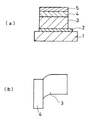
図1は本発明の1実施例の概略を示す図である。図1(a)には、本発明の太陽電池の構造の断面図を示しており、(b)にはヘテロ接合部(傾斜組成層を含む)のバンド図を示し、(b)中の破線は、従来構造のヘテロ接合型太陽電池の場合(傾斜組成層のないもの)における接合のバンド図である。バンドベンディングを生じている領域pは、空乏層を示している。
【0019】
図1において1はガラス基板などの絶縁基板であり、この基板1に下部電極2としてMo薄膜が膜厚1μm程度に成膜され、この下部電極2の上に透明上部電極としてITO薄膜5が膜厚0.5μm程度に成膜されている。本発明の太陽電池の根幹をなす半導体窓層4/傾斜組成層6/半導体光吸収層3の構造は、CdS半導体窓層4(膜厚0.1μm)/CdTe1ーXSeX傾斜組成層6/CdTe半導体光吸収層3(膜厚3μm)によって構成されている。この構造において、CdS層に接するCdTe1ーXSeX層のXの値は0.20であり、CdTe層に接するCdTe1ーXSeX層のXの値は0.0である。また、CdTe1ーXSeX層の膜厚は、空乏層幅pとほぼ同程度になるように、例えば0.2〜1.0μmに最適設計する。
【0020】
CdTe1ーXSeXの傾斜組成層6の膜厚が、空乏層領域に比べ薄い場合は、短絡光電流が充分獲得できなくなり、空乏層領域に比べ厚い場合は、開放端電圧が低下する傾向がある。以上のように、CdTe1ーXSeXの傾斜組成層6の膜厚を最適化した本発明の構造の太陽電池を多元蒸着装置を用いて作製し、同様に多元蒸着で作製した従来のCdTe1ーXSeX傾斜組成層のない太陽電池と性能を比較した。
【0021】
ここで作製したCdTe1ーXSeX傾斜組成層6はp型でそのホール濃度は、CdTe薄膜と同様に約1×1015cm-3であったので、CdTe1ーXSeX傾斜組成層の膜厚は、0.7μm程度にした。
【0022】
図3に本実施例による太陽電池の量子効率の波長依存性をA’で示し、比較のため従来例の太陽電池による量子効率の波長依存性をAで示した。両者の量子効率には差異がなく、ほとんど同程度の短絡光電流が期待できる。
【0023】
図4には、AM1.5、100mW/cm2のソーラーシミュレーターのもとで測定した電流−電圧特性を示している。従来構造の太陽電池の特性Aに比べ、本発明の太陽電池の特性A’の方が高い開放端電圧が得られた。この効果は、傾斜組成層を導入することによってヘテロ接合部の再結合電流が減少し、従来のヘテロ接合に比べてより高い開放端電圧を出力できる太陽電池が実現できたことを示している。得られた変換効率は、従来例の太陽電池で12.2%(Jsc=22.5mA/cm2, Voc=0.750V,FF=0.720)、本実施例の太陽電池で14.1%(Jsc=22.2mA/cm2,Voc=0.890V,FF=0.715)であった。
【0024】
(実施例2)
前記実施例1の太陽電池の構造と同様に、ガラス基板などの絶縁基板1に下部電極2としてMo薄膜が膜厚1μm程度に成膜され、この下部電極2の上に透明上部電極としてITO薄膜5が膜厚0.5μm程度に成膜されている。この上に本発明の太陽電池の根幹をなす半導体窓層4/傾斜組成層6/半導体光吸収層3の層が形成されている。本実施例でも上記実施例と同様に、半導体窓層4がCdSにより膜厚0.1μmに形成されている。
【0025】
ただし、本実施例では、傾斜組成層6をCuIn1ーXGaXSe2 から形成し、半導体光吸収層3はCuInSe2 から膜厚2μmに形成している点で上記実施例1とは異なっている。また、本実施例のCdS半導体窓層4に接するCuIn1ーXGaXSe2傾斜組成層6のXの値は0.15であり、CuInSe2層に接するCuIn1ーXGaXSe2層のXの値は0.0である。また、CuIn1ーXGaX Se2 層の膜厚は、空乏層幅pとほぼ同程度になるよう最適設計する必要がある。CuIn1ーXGaXSe2 層の膜厚が、空乏層領域に比べ薄い場合は、短絡光電流が充分獲得できなくなり、空乏層領域に比べ厚い場合は、開放端電圧が低下する傾向がある。従って、この傾斜組成層6の膜厚は、例えば、0.2〜1.0μmとする。
【0026】
以上のように、CuIn1ーXGaXSe2 傾斜組成層の膜厚を最適化した本発明の構造の太陽電池を多元蒸着装置を用いて作製し、同様に多元蒸着で作製した従来のCuIn1ーXGaXSe2 傾斜組成層のない太陽電池と性能を比較した。ここで作製したCuIn1ーXGaXSe2 傾斜組成層はp型でそのホール濃度は、CuInSe2薄膜と同様に約5×1015cm-3であったのでCuIn1ーXGaXS2傾斜組成層の膜厚は、0.3μm程度にした。
【0027】
本実施例の太陽電池と従来例とについて、量子効率の波長依存性のを図3のB、B’(B:従来構造、B’:本発明の構造)に示している。この両者には差異がなく、ほとんど同程度の短絡光電流が得られている。
【0028】
図4には、AM1.5、100mW/cm2のソーラーシミュレーターのもとで測定した電流−電圧特性を示している。従来構造の太陽電池の特性Bに比べ、本発明の太陽電池の特性B’の方が高い開放端電圧を示していた。この効果は、傾斜組成層を導入することによってヘテロ接合部の再結合電流が減少し、従来のヘテロ接合に比べてより高い開放端電圧を出力できる太陽電池が実現できたことを示している。得られた変換効率は、従来構造の太陽電池で13.1%(Jsc=40.5mA/cm2,Voc=0.455V,FF=0.710)、本実施例による太陽電池で 15.3%(Jsc=40.4mA/cm2,Voc=0.528V,FF=0.715)であった。
【0029】
(実施例3)
前記実施例1の太陽電池の構造と同様に、ガラス基板などの絶縁基板1に下部電極2としてMo薄膜が膜厚1μm程度に成膜され、この下部電極2の上に透明上部電極としてITO薄膜5が膜厚0.5μm程度に成膜されている。この上に、本発明の太陽電池の根幹をなす半導体窓層4/傾斜組成層6/半導体光吸収層3の層が形成されている。本実施例でも上記実施例と同様に、半導体窓層4がCdSにより膜厚0.1μmに形成されている。
【0030】
ただし、本実施例では、傾斜組成層6をCuIn(Se1ーX SX )2 から形成し、半導体光吸収層3はCuInSe2 から膜厚2μmに形成している点で上記実施例1および実施例2とは異なっている。また、本実施例のCdS層に接するCuIn(Se1ーX SX )2 傾斜組成層6のXの値は0.20であり、CuInSe2 半導体光吸収層3に接するCuIn(Se1ーXSX )2のXの値は0.0である。また、CuIn(Se1ーX SX)2の膜厚は、空乏層幅pとほぼ同程度になるよう最適設計する必要がある。CuIn(Se1ーX SX )2 層の膜厚が、空乏層領域に比べ薄い場合は、短絡光電流が充分獲得できなくなり、空乏層領域に比べ厚い場合は、開放端電圧が低下する傾向がある。従って、この傾斜組成層6の膜厚は、例えば、0.2〜1.0μmとする。
【0031】
以上のように、CuIn(Se1ーXSX)2 の傾斜組成層6の膜厚を最適化した本発明の構造の太陽電池を多元蒸着装置を用いて作製し、同様に多元蒸着で作製した従来のCuIn(Se1ーXSX)2 傾斜組成層のない太陽電池と性能を比較した。ここで作製したCuIn(Se1ーXSX)2 傾斜組成層6はp型でそのホール濃度は、CuInSe2 薄膜と同様に約2×1015cm-3であったので、CuIn1ーXGaXSe2 傾斜組成層6の膜厚は0.3μm程度にした。
【0032】
本実施例の太陽電池と従来例とについて、量子効率の波長依存性のを図3のC、C’(C:従来構造、C’:本実施例の構造)に示している。この両者には差異がなく、ほとんど同程度の短絡光電流が得られている。
【0033】
図4には、AM1.5、100mW/cm2のソーラーシミュレーターのもとで測定した電流−電圧特性を示している。従来構造の太陽電池の特性Cに比べ、本実施例の太陽電池の特性C’の方が高い開放端電圧を示していた。この効果は、傾斜組成層を導入することによってヘテロ接合部の再結合電流が減少し、従来のヘテロ接合に比べてより高い開放端電圧を出力できる太陽電池が実現できたことを示している。得られた変換効率は、従来構造の太陽電池で13.1%(Jsc=40.5mA/cm2,Voc=0.455V,FF=0.710)、本実施例による太陽電池で15.1%(Jsc=40.2mA/cm2,Voc=0.555V,FF=0.675)であった。
【0034】
【発明の効果】
上述のように、本発明の太陽電池によれば半導体光吸収層と半導体窓層の間に該半導体窓層との接合部より離れるに従ってバンドギャップが小さくなり、かつ前記半導体光吸収層に接する部分のバンドギャップが該半導体光吸収層のバンドギャップに比べて同等もしくは大きい傾斜組成層を有し、かつその膜厚が空乏層幅と同等の膜厚よりなっているので、ヘテロ接合部の再結合電流が減少し、高い解放電圧を得ることができ、エネルギー変換効率を高くすることができる。
【図面の簡単な説明】
【図1】本発明の太陽電池の構造を示す断面図である。
【図2】従来の太陽電池の構造を示す断面図である。
【図3】従来及び本発明の太陽電池の量子効率の波長依存性を示す図である。
【図4】従来及び本発明の太陽電池の太陽電池特性(電流−電圧特性)を示す図である。
【符号の説明】
1 絶縁基板
2 下部電極
3 半導体光吸収層
4 半導体窓層
5 透明導電層
6 傾斜組成層[0001]
[Industrial application fields]
The present invention relates to a solar cell with high conversion efficiency. More specifically, the present invention relates to a heterojunction solar cell having a wide band gap structure.
[0002]
[Prior art]
Conventionally, many proposals have been made on the basic structure of a solar cell. A typical heterojunction solar cell includes a semiconductor (window layer) 4 having a wide band gap as shown in FIG. 2A and a semiconductor (light absorption) having a band gap of about 1.5 eV (or lower). Layer) and a band profile as shown in FIG. 2B. For example, CdS / CdTe and CdS / CuInSe 2 are used. Furthermore, proposals have been made to introduce a gradient composition layer into the structure of a solar cell in order to obtain high conversion efficiency. In many cases, it is introduced into a semiconductor (window layer) having a large band gap. For example, a-SiC / a-Si and AlGaAs / GaAs structures are examples. These structures are structures in which a gradient composition layer is introduced into a semiconductor (window layer) having a large band gap to acquire more photocurrent.
[0003]
[Problems to be Solved by the Invention]
However, even in the conventional heterojunction solar cell, the light-power conversion efficiency was about 12.2 to 13.1%.
[0004]
The object of the present invention has been made in view of the problems of the prior art, and is to provide a solar cell with further improved performance.
[0005]
[Means for Solving the Problems]
In order to solve the above problems, a solar cell of the present invention includes a semiconductor light absorption layer, an electrode for the semiconductor light absorption layer, a band formed on the semiconductor light absorption layer and wider than the band gap of the semiconductor light absorption layer. a semiconductor window layer having a conductivity type different gap and said semiconductor light absorption layer, a solar cell and a transparent electrode for the semiconductor window layer, formed between said semiconductor optical absorption layer and the semiconductor window layer, in contact with the said semiconductor light absorption layer and said semiconductor window layer is the same conductivity type as said semiconductor light absorption layer, the band gap becomes smaller with distance from the junction between the semiconductor window layer, and to the semiconductor optical absorption layer contact band gap of the portion further has a equal to or larger gradient composition layer than to the bandgap of the semiconductor light absorption layer, the thickness of the graded composition layer is ne than comparable thickness and width of the depletion layer It is characterized in.
[0006]
In the solar cell having the above-described configuration, it is preferable that the semiconductor light absorption layer is made of a CdTe thin film, and the gradient composition layer is made of CdTe 1-X Se X.
In the solar cell having the above structure, it is preferable that the semiconductor window layer is made of a CdS thin film, the semiconductor light absorption layer is made of a CdTe thin film, and the gradient composition layer is made of CdTe 1-X Se X.
[0007]
In the solar cell having the above-described configuration, it is preferable that the semiconductor light absorption layer is made of a CuInSe 2 thin film, and the gradient composition layer is made of CuIn 1−X Ga x Se 2 .
Further, in the solar cell having the above-described configuration, the semiconductor window layer is made of a CdS thin film, the semiconductor light absorption layer is made of a CuInSe 2 thin film, and the gradient composition layer is made of CuIn 1−X Ga X Se 2. preferable.
[0008]
In the solar cell having the above structure, it is preferable that the semiconductor light absorption layer is made of a CuInSe 2 thin film, and the gradient composition layer is made of CuIn (Se 1−X S X ) 2 .
[0009]
Further, in the solar cell having the above configuration, the semiconductor window layer is made of a CdS thin film, the semiconductor light absorption layer is made of a CuInSe 2 thin film, and the gradient composition layer is made of CuIn (Se 1−X S X ) 2. It is preferable.
[0010]
[Action]
The solar cell of the present invention includes a semiconductor light absorption layer, an electrode for the semiconductor light absorption layer, a band gap formed on the semiconductor light absorption layer, wider than the band gap of the semiconductor light absorption layer, and the semiconductor light absorption layer and a semiconductor window layer having a different conductivity type, a solar cell and a transparent electrode for the semiconductor window layer, formed between said semiconductor optical absorption layer and the semiconductor window layer, the semiconductor light absorption layer and the in contact with a semiconductor window layer, the same conductivity type as said semiconductor light absorption layer, the band gap becomes smaller with distance from the junction between the semiconductor window layer, and the band gap of the portion in contact with said semiconductor light absorption layer is the A gradient composition layer that is equal to or larger than the band gap of the semiconductor light absorption layer is further provided, and the thickness of the gradient composition layer is equal to the thickness of the depletion layer. With this configuration, the recombination current at the heterojunction portion is reduced, and a high open- circuit voltage can be obtained.
[0011]
Further, in the configuration of the solar cell, according to a preferred configuration in which the semiconductor light absorption layer is made of a CdTe thin film and the gradient composition layer is made of CdTe 1-X Se X , the recombination current of the heterojunction portion is reduced. Compared with a conventional heterojunction, a higher open-circuit voltage can be output, and a conversion efficiency superior to that of a conventional solar cell can be obtained.
[0012]
Further, in the configuration of the solar cell, the semiconductor window layer is made of CdS thin film, the semiconductor light absorption layer is made of CdTe thin film, since the graded composition layer is formed of CdTe 1 over X Se X, the use of CdS thin film Therefore, it is possible to maintain a higher quality junction, reduce a recombination current, output a higher open-circuit voltage than a conventional junction, and obtain a conversion efficiency superior to that of a conventional solar cell.
[0013]
Moreover, in the solar cell having the above-described configuration, according to a preferred mode in which the semiconductor light absorption layer is made of a CuInSe 2 thin film and the gradient composition layer is made of CuIn 1-X Ga X Se 2, As a result, the open-circuit voltage higher than that of the conventional heterojunction can be output, and the conversion efficiency superior to that of the conventional solar cell can be obtained.
[0014]
In the solar cell having the above-described configuration, the semiconductor window layer is made of a CdS thin film, the semiconductor light absorption layer is made of a CuInSe 2 thin film, and the gradient composition layer is made of CuIn 1-X Ga X Se 2. For example, CdS thin film can be used to maintain a higher quality junction, reduce recombination current, output higher open-circuit voltage than conventional junctions, and have better conversion efficiency than conventional solar cells Can be obtained.
[0015]
Moreover, in the solar cell having the above-described configuration, the semiconductor light absorption layer is made of a CuInSe 2 thin film, and the gradient composition layer is made of CuIn (Se 1−X S X ) 2. As a result, the open-circuit voltage higher than that of the conventional heterojunction can be output, and the conversion efficiency superior to that of the conventional solar cell can be obtained.
[0016]
Further, in the solar cell having the above configuration, the semiconductor window layer is made of a CdS thin film, the semiconductor light absorption layer is made of a CuInSe 2 thin film, and the gradient composition layer is made of CuIn (Se 1−X S X ) 2. Therefore, by using CdS thin film, it is possible to maintain a higher quality junction, reduce recombination current, output higher open-circuit voltage than conventional junction, and have superior conversion efficiency than conventional solar cells. Can be obtained.
[0017]
That is, in the solar cell of the present invention, since the graded composition layer is introduced as described above, the recombination current of the heterojunction is reduced without affecting the wavelength dependence of the quantum efficiency, and the conventional heterogeneity is reduced. A solar cell that can output a higher open-circuit voltage than a junction can be realized, and at the same time, the photocurrent is not inferior to that of a conventional heterojunction solar cell.
[0018]
【Example】
Embodiments of the solar cell of the present invention will be described below with reference to the drawings.
(Example 1)
FIG. 1 is a diagram showing an outline of one embodiment of the present invention. FIG. 1A shows a cross-sectional view of the structure of the solar cell of the present invention, FIG. 1B shows a band diagram of a heterojunction (including a gradient composition layer), and a broken line in FIG. These are the band diagrams of a junction in the case of the heterojunction type solar cell of a conventional structure (one without a graded composition layer). A region p where band bending is generated indicates a depletion layer.
[0019]
In FIG. 1, reference numeral 1 denotes an insulating substrate such as a glass substrate. A Mo thin film is formed on the substrate 1 as a
[0020]
When the
[0021]
The CdTe 1-X Se X graded
[0022]
In FIG. 3, the wavelength dependence of the quantum efficiency of the solar cell according to this example is indicated by A ′, and the wavelength dependence of the quantum efficiency by the solar cell of the conventional example is indicated by A for comparison. There is no difference in quantum efficiency between the two, and almost the same short-circuit photocurrent can be expected.
[0023]
FIG. 4 shows current-voltage characteristics measured under a solar simulator of AM 1.5, 100 mW / cm 2 . Compared with the characteristic A of the solar cell having the conventional structure, a higher open-circuit voltage was obtained with the characteristic A ′ of the solar cell of the present invention. This effect indicates that by introducing the graded composition layer, the recombination current at the heterojunction portion is reduced, and a solar cell that can output a higher open-circuit voltage than a conventional heterojunction can be realized. The conversion efficiency obtained was 12.2% (Jsc = 22.5mA / cm 2 , Voc = 0.750V, FF = 0.720) for the conventional solar cell, and 14.1% (Jsc = 22.2 mA / cm 2 , Voc = 0.890V, FF = 0.715).
[0024]
(Example 2)
Similar to the structure of the solar cell of Example 1, a Mo thin film is formed as a
[0025]
However, in this embodiment, the
[0026]
As described above, the conventional CuIn produced by using the multi-source deposition apparatus and the solar cell having the structure of the present invention in which the film thickness of the CuIn 1 -X Ga X Se 2 graded composition layer is optimized is manufactured using the multi-source deposition apparatus. The performance was compared with a solar cell without a 1-X Ga X Se 2 graded composition layer. Here CuIn to prepare 1 over X Ga X Se 2 graded composition layer that hole concentration in p-type, CuIn 1 over X Ga X S 2 so was about 5 × 10 15 cm -3 like the CuInSe 2 thin film The thickness of the gradient composition layer was about 0.3 μm.
[0027]
For the solar cell of this example and the conventional example, the wavelength dependence of the quantum efficiency is shown in B and B ′ (B: conventional structure, B ′: structure of the present invention) in FIG. There is no difference between them, and almost the same short-circuit photocurrent is obtained.
[0028]
FIG. 4 shows current-voltage characteristics measured under a solar simulator of AM 1.5, 100 mW / cm 2 . Compared with the characteristic B of the solar cell having the conventional structure, the characteristic B ′ of the solar cell of the present invention showed a higher open-circuit voltage. This effect indicates that by introducing the graded composition layer, the recombination current at the heterojunction portion is reduced, and a solar cell that can output a higher open-circuit voltage than a conventional heterojunction can be realized. The conversion efficiency obtained was 13.1% (Jsc = 40.5 mA / cm 2 , Voc = 0.455V, FF = 0.710) for the solar cell of the conventional structure, and 15.3% (Jsc = 40.4mA / cm 2 , Voc = 0.528V, FF = 0.715).
[0029]
(Example 3)
Similar to the structure of the solar cell of Example 1, a Mo thin film is formed as a
[0030]
However, in this example, the
[0031]
As described above, the solar cell having the structure of the present invention in which the film thickness of the
[0032]
The wavelength dependence of the quantum efficiency of the solar cell of this example and the conventional example is shown in C and C ′ (C: conventional structure, C ′: structure of this example) in FIG. There is no difference between them, and almost the same short-circuit photocurrent is obtained.
[0033]
FIG. 4 shows current-voltage characteristics measured under a solar simulator of AM 1.5, 100 mW / cm 2 . Compared with the characteristic C of the solar cell of the conventional structure, the characteristic C ′ of the solar cell of this example showed a higher open-circuit voltage. This effect indicates that by introducing the graded composition layer, the recombination current at the heterojunction portion is reduced, and a solar cell that can output a higher open-circuit voltage than a conventional heterojunction can be realized. The conversion efficiency obtained was 13.1% (Jsc = 40.5 mA / cm 2 , Voc = 0.455V, FF = 0.710) for the solar cell of the conventional structure, and 15.1% (Jsc = 40.2 mA / cm 2 , Voc = 0.555V, FF = 0.675).
[0034]
【The invention's effect】
As described above, according to the solar cell of the present invention, the band gap is reduced between the semiconductor light absorption layer and the semiconductor window layer as the distance from the junction with the semiconductor window layer decreases, and the portion in contact with the semiconductor light absorption layer The band gap of the heterojunction has a graded composition layer that is equal to or larger than the band gap of the semiconductor light absorption layer and the film thickness is equal to the depletion layer width. The current decreases, a high release voltage can be obtained, and the energy conversion efficiency can be increased.
[Brief description of the drawings]
FIG. 1 is a cross-sectional view showing the structure of a solar cell of the present invention.
FIG. 2 is a cross-sectional view showing the structure of a conventional solar cell.
FIG. 3 is a graph showing wavelength dependence of quantum efficiency of conventional and solar cells of the present invention.
FIG. 4 is a graph showing solar cell characteristics (current-voltage characteristics) of a conventional and the solar cell of the present invention.
[Explanation of symbols]
DESCRIPTION OF SYMBOLS 1
Claims (7)
Priority Applications (1)
| Application Number | Priority Date | Filing Date | Title |
|---|---|---|---|
| JP26877294A JP3646940B2 (en) | 1994-11-01 | 1994-11-01 | Solar cell |
Applications Claiming Priority (1)
| Application Number | Priority Date | Filing Date | Title |
|---|---|---|---|
| JP26877294A JP3646940B2 (en) | 1994-11-01 | 1994-11-01 | Solar cell |
Publications (2)
| Publication Number | Publication Date |
|---|---|
| JPH08130321A JPH08130321A (en) | 1996-05-21 |
| JP3646940B2 true JP3646940B2 (en) | 2005-05-11 |
Family
ID=17463092
Family Applications (1)
| Application Number | Title | Priority Date | Filing Date |
|---|---|---|---|
| JP26877294A Expired - Lifetime JP3646940B2 (en) | 1994-11-01 | 1994-11-01 | Solar cell |
Country Status (1)
| Country | Link |
|---|---|
| JP (1) | JP3646940B2 (en) |
Families Citing this family (15)
| Publication number | Priority date | Publication date | Assignee | Title |
|---|---|---|---|---|
| JP4320525B2 (en) * | 2002-03-25 | 2009-08-26 | 本田技研工業株式会社 | Method and apparatus for producing light absorption layer |
| DE102008024230A1 (en) * | 2008-05-19 | 2009-11-26 | Avancis Gmbh & Co. Kg | Layer system for solar cells |
| US20120104460A1 (en) | 2010-11-03 | 2012-05-03 | Alta Devices, Inc. | Optoelectronic devices including heterojunction |
| EP2351097A2 (en) | 2008-10-23 | 2011-08-03 | Alta Devices, Inc. | Photovoltaic device |
| US9691921B2 (en) | 2009-10-14 | 2017-06-27 | Alta Devices, Inc. | Textured metallic back reflector |
| US9502594B2 (en) | 2012-01-19 | 2016-11-22 | Alta Devices, Inc. | Thin-film semiconductor optoelectronic device with textured front and/or back surface prepared from template layer and etching |
| US20150380576A1 (en) | 2010-10-13 | 2015-12-31 | Alta Devices, Inc. | Optoelectronic device with dielectric layer and method of manufacture |
| US9768329B1 (en) | 2009-10-23 | 2017-09-19 | Alta Devices, Inc. | Multi-junction optoelectronic device |
| US20170141256A1 (en) | 2009-10-23 | 2017-05-18 | Alta Devices, Inc. | Multi-junction optoelectronic device with group iv semiconductor as a bottom junction |
| US11271128B2 (en) | 2009-10-23 | 2022-03-08 | Utica Leaseco, Llc | Multi-junction optoelectronic device |
| EP2590224B1 (en) * | 2010-06-30 | 2019-06-05 | Kyocera Corporation | Photoelectric conversion device |
| JP5784358B2 (en) * | 2011-05-06 | 2015-09-24 | 株式会社東芝 | Photoelectric conversion element and solar cell |
| US11038080B2 (en) | 2012-01-19 | 2021-06-15 | Utica Leaseco, Llc | Thin-film semiconductor optoelectronic device with textured front and/or back surface prepared from etching |
| US11450778B2 (en) | 2016-05-31 | 2022-09-20 | First Solar, Inc. | Ag-doped photovoltaic devices and method of making |
| WO2022074852A1 (en) * | 2020-10-09 | 2022-04-14 | 株式会社 東芝 | Solar cell, multi-junction solar cell, solar cell module, and solar power generation system |
-
1994
- 1994-11-01 JP JP26877294A patent/JP3646940B2/en not_active Expired - Lifetime
Also Published As
| Publication number | Publication date |
|---|---|
| JPH08130321A (en) | 1996-05-21 |
Similar Documents
| Publication | Publication Date | Title |
|---|---|---|
| US4547622A (en) | Solar cells and photodetectors | |
| KR100974226B1 (en) | Backside surface passivation and reflection layer for Si solar cell by high-k dielectrics | |
| KR100974220B1 (en) | Solar cell | |
| US4496788A (en) | Photovoltaic device | |
| US6300557B1 (en) | Low-bandgap double-heterostructure InAsP/GaInAs photovoltaic converters | |
| US5376185A (en) | Single-junction solar cells with the optimum band gap for terrestrial concentrator applications | |
| JP3646940B2 (en) | Solar cell | |
| US20110056544A1 (en) | Solar cell | |
| JPH05114747A (en) | Improved monolithic tandem-type solar cell | |
| CN101740663A (en) | Method of manufacturing solar cell | |
| JPH09199738A (en) | Solar cell | |
| US20240065008A1 (en) | Solar battery | |
| JP3444700B2 (en) | Solar cell | |
| JP3130993B2 (en) | Solar cell | |
| Kao et al. | Performance enhancement of III–V multi-junction solar cells using indium-tin-oxide electrodes | |
| JP2632740B2 (en) | Amorphous semiconductor solar cell | |
| JPH0955522A (en) | Tunnel diode | |
| JPS6249754B2 (en) | ||
| JPH05218477A (en) | Solar cell | |
| KR101989738B1 (en) | Compound semiconductor solar cell and method of manufacturing the same | |
| JPH07231108A (en) | Solar cell | |
| KR920009897B1 (en) | Amorphous silicon solar cell | |
| JP3133449B2 (en) | Solar cell | |
| Kamruzzaman et al. | Optimization of Different III-V Multiple Quantum Well Solar Cells with Surficial Circular Nanoholes | |
| Kurtz et al. | DESIGN OF HIGH-EFFICIENCY, RADIATION-HARD, GaInP/GaAs SOLAR CELLS¹ |
Legal Events
| Date | Code | Title | Description |
|---|---|---|---|
| A131 | Notification of reasons for refusal |
Free format text: JAPANESE INTERMEDIATE CODE: A131 Effective date: 20040206 |
|
| A521 | Request for written amendment filed |
Free format text: JAPANESE INTERMEDIATE CODE: A523 Effective date: 20040401 |
|
| TRDD | Decision of grant or rejection written | ||
| A01 | Written decision to grant a patent or to grant a registration (utility model) |
Free format text: JAPANESE INTERMEDIATE CODE: A01 Effective date: 20050203 |
|
| A61 | First payment of annual fees (during grant procedure) |
Free format text: JAPANESE INTERMEDIATE CODE: A61 Effective date: 20050204 |
|
| R150 | Certificate of patent or registration of utility model |
Free format text: JAPANESE INTERMEDIATE CODE: R150 |
|
| FPAY | Renewal fee payment (event date is renewal date of database) |
Free format text: PAYMENT UNTIL: 20080218 Year of fee payment: 3 |
|
| FPAY | Renewal fee payment (event date is renewal date of database) |
Free format text: PAYMENT UNTIL: 20090218 Year of fee payment: 4 |
|
| FPAY | Renewal fee payment (event date is renewal date of database) |
Free format text: PAYMENT UNTIL: 20100218 Year of fee payment: 5 |
|
| FPAY | Renewal fee payment (event date is renewal date of database) |
Free format text: PAYMENT UNTIL: 20100218 Year of fee payment: 5 |
|
| FPAY | Renewal fee payment (event date is renewal date of database) |
Free format text: PAYMENT UNTIL: 20110218 Year of fee payment: 6 |
|
| FPAY | Renewal fee payment (event date is renewal date of database) |
Free format text: PAYMENT UNTIL: 20120218 Year of fee payment: 7 |
|
| FPAY | Renewal fee payment (event date is renewal date of database) |
Free format text: PAYMENT UNTIL: 20130218 Year of fee payment: 8 |
|
| FPAY | Renewal fee payment (event date is renewal date of database) |
Free format text: PAYMENT UNTIL: 20130218 Year of fee payment: 8 |
|
| FPAY | Renewal fee payment (event date is renewal date of database) |
Free format text: PAYMENT UNTIL: 20140218 Year of fee payment: 9 |
|
| EXPY | Cancellation because of completion of term |