JP2015043438A - Substrate for integrated circuit devices including multi-layer glass core and methods of making the same - Google Patents
Substrate for integrated circuit devices including multi-layer glass core and methods of making the same Download PDFInfo
- Publication number
- JP2015043438A JP2015043438A JP2014192658A JP2014192658A JP2015043438A JP 2015043438 A JP2015043438 A JP 2015043438A JP 2014192658 A JP2014192658 A JP 2014192658A JP 2014192658 A JP2014192658 A JP 2014192658A JP 2015043438 A JP2015043438 A JP 2015043438A
- Authority
- JP
- Japan
- Prior art keywords
- layer
- glass
- core
- layers
- substrate
- Prior art date
- Legal status (The legal status is an assumption and is not a legal conclusion. Google has not performed a legal analysis and makes no representation as to the accuracy of the status listed.)
- Pending
Links
- 239000011521 glass Substances 0.000 title claims abstract description 314
- 239000000758 substrate Substances 0.000 title claims abstract description 114
- 238000000034 method Methods 0.000 title claims description 145
- 239000004020 conductor Substances 0.000 claims abstract description 57
- 239000010410 layer Substances 0.000 claims description 482
- 229910052751 metal Inorganic materials 0.000 claims description 101
- 239000002184 metal Substances 0.000 claims description 101
- 230000008569 process Effects 0.000 claims description 47
- 239000011241 protective layer Substances 0.000 claims description 30
- 238000000151 deposition Methods 0.000 claims description 6
- 238000007747 plating Methods 0.000 claims description 5
- 230000008878 coupling Effects 0.000 claims description 3
- 238000010168 coupling process Methods 0.000 claims description 3
- 238000005859 coupling reaction Methods 0.000 claims description 3
- 230000000149 penetrating effect Effects 0.000 claims 1
- 238000010586 diagram Methods 0.000 description 54
- 239000000463 material Substances 0.000 description 50
- 230000015572 biosynthetic process Effects 0.000 description 20
- 239000000853 adhesive Substances 0.000 description 18
- 230000001070 adhesive effect Effects 0.000 description 18
- 150000002739 metals Chemical class 0.000 description 15
- 239000003989 dielectric material Substances 0.000 description 14
- PXHVJJICTQNCMI-UHFFFAOYSA-N Nickel Chemical compound [Ni] PXHVJJICTQNCMI-UHFFFAOYSA-N 0.000 description 12
- 238000005530 etching Methods 0.000 description 12
- RYGMFSIKBFXOCR-UHFFFAOYSA-N Copper Chemical compound [Cu] RYGMFSIKBFXOCR-UHFFFAOYSA-N 0.000 description 10
- 239000012790 adhesive layer Substances 0.000 description 10
- 229910052802 copper Inorganic materials 0.000 description 10
- 239000010949 copper Substances 0.000 description 10
- 229910000679 solder Inorganic materials 0.000 description 10
- 229910052782 aluminium Inorganic materials 0.000 description 8
- XAGFODPZIPBFFR-UHFFFAOYSA-N aluminium Chemical compound [Al] XAGFODPZIPBFFR-UHFFFAOYSA-N 0.000 description 8
- 238000004519 manufacturing process Methods 0.000 description 8
- 238000005229 chemical vapour deposition Methods 0.000 description 7
- BQCADISMDOOEFD-UHFFFAOYSA-N Silver Chemical compound [Ag] BQCADISMDOOEFD-UHFFFAOYSA-N 0.000 description 6
- 229910045601 alloy Inorganic materials 0.000 description 6
- 239000000956 alloy Substances 0.000 description 6
- 238000007772 electroless plating Methods 0.000 description 6
- 238000009713 electroplating Methods 0.000 description 6
- 239000010408 film Substances 0.000 description 6
- 230000009477 glass transition Effects 0.000 description 6
- 229910052759 nickel Inorganic materials 0.000 description 6
- 238000005240 physical vapour deposition Methods 0.000 description 6
- 229910052709 silver Inorganic materials 0.000 description 6
- 239000004332 silver Substances 0.000 description 6
- 239000011248 coating agent Substances 0.000 description 5
- 238000000576 coating method Methods 0.000 description 5
- 238000009792 diffusion process Methods 0.000 description 5
- 238000005553 drilling Methods 0.000 description 5
- PCHJSUWPFVWCPO-UHFFFAOYSA-N gold Chemical compound [Au] PCHJSUWPFVWCPO-UHFFFAOYSA-N 0.000 description 5
- 229910052737 gold Inorganic materials 0.000 description 5
- 239000010931 gold Substances 0.000 description 5
- 239000007788 liquid Substances 0.000 description 5
- 239000000203 mixture Substances 0.000 description 5
- 230000002093 peripheral effect Effects 0.000 description 5
- 238000005488 sandblasting Methods 0.000 description 5
- VYPSYNLAJGMNEJ-UHFFFAOYSA-N silicon dioxide Inorganic materials O=[Si]=O VYPSYNLAJGMNEJ-UHFFFAOYSA-N 0.000 description 5
- 238000004381 surface treatment Methods 0.000 description 5
- 239000002131 composite material Substances 0.000 description 4
- 229920001940 conductive polymer Polymers 0.000 description 4
- 239000005340 laminated glass Substances 0.000 description 4
- 238000003475 lamination Methods 0.000 description 4
- 239000011368 organic material Substances 0.000 description 4
- 239000007787 solid Substances 0.000 description 4
- KRHYYFGTRYWZRS-UHFFFAOYSA-N Fluorane Chemical compound F KRHYYFGTRYWZRS-UHFFFAOYSA-N 0.000 description 3
- CDBYLPFSWZWCQE-UHFFFAOYSA-L Sodium Carbonate Chemical compound [Na+].[Na+].[O-]C([O-])=O CDBYLPFSWZWCQE-UHFFFAOYSA-L 0.000 description 3
- 239000000654 additive Substances 0.000 description 3
- 238000004026 adhesive bonding Methods 0.000 description 3
- 239000003990 capacitor Substances 0.000 description 3
- 230000008021 deposition Effects 0.000 description 3
- 238000001312 dry etching Methods 0.000 description 3
- 239000002861 polymer material Substances 0.000 description 3
- 238000012545 processing Methods 0.000 description 3
- 238000007650 screen-printing Methods 0.000 description 3
- 239000002904 solvent Substances 0.000 description 3
- 239000000126 substance Substances 0.000 description 3
- 239000004925 Acrylic resin Substances 0.000 description 2
- 229920000178 Acrylic resin Polymers 0.000 description 2
- VTYYLEPIZMXCLO-UHFFFAOYSA-L Calcium carbonate Chemical compound [Ca+2].[O-]C([O-])=O VTYYLEPIZMXCLO-UHFFFAOYSA-L 0.000 description 2
- OKTJSMMVPCPJKN-UHFFFAOYSA-N Carbon Chemical compound [C] OKTJSMMVPCPJKN-UHFFFAOYSA-N 0.000 description 2
- VYZAMTAEIAYCRO-UHFFFAOYSA-N Chromium Chemical compound [Cr] VYZAMTAEIAYCRO-UHFFFAOYSA-N 0.000 description 2
- XEEYBQQBJWHFJM-UHFFFAOYSA-N Iron Chemical compound [Fe] XEEYBQQBJWHFJM-UHFFFAOYSA-N 0.000 description 2
- XUIMIQQOPSSXEZ-UHFFFAOYSA-N Silicon Chemical compound [Si] XUIMIQQOPSSXEZ-UHFFFAOYSA-N 0.000 description 2
- ATJFFYVFTNAWJD-UHFFFAOYSA-N Tin Chemical compound [Sn] ATJFFYVFTNAWJD-UHFFFAOYSA-N 0.000 description 2
- 239000002313 adhesive film Substances 0.000 description 2
- 238000000231 atomic layer deposition Methods 0.000 description 2
- 230000008901 benefit Effects 0.000 description 2
- 229910052799 carbon Inorganic materials 0.000 description 2
- 229910052804 chromium Inorganic materials 0.000 description 2
- 239000011651 chromium Substances 0.000 description 2
- 238000010276 construction Methods 0.000 description 2
- 239000003822 epoxy resin Substances 0.000 description 2
- -1 for example Substances 0.000 description 2
- 230000007246 mechanism Effects 0.000 description 2
- 229920000620 organic polymer Polymers 0.000 description 2
- 238000002161 passivation Methods 0.000 description 2
- 238000000059 patterning Methods 0.000 description 2
- 238000000206 photolithography Methods 0.000 description 2
- 229920002120 photoresistant polymer Polymers 0.000 description 2
- 230000000704 physical effect Effects 0.000 description 2
- 239000011295 pitch Substances 0.000 description 2
- BASFCYQUMIYNBI-UHFFFAOYSA-N platinum Chemical compound [Pt] BASFCYQUMIYNBI-UHFFFAOYSA-N 0.000 description 2
- 229920000647 polyepoxide Polymers 0.000 description 2
- 229910052710 silicon Inorganic materials 0.000 description 2
- 239000010703 silicon Substances 0.000 description 2
- 239000000377 silicon dioxide Substances 0.000 description 2
- 239000005361 soda-lime glass Substances 0.000 description 2
- 229910052718 tin Inorganic materials 0.000 description 2
- 239000011135 tin Substances 0.000 description 2
- WFKWXMTUELFFGS-UHFFFAOYSA-N tungsten Chemical compound [W] WFKWXMTUELFFGS-UHFFFAOYSA-N 0.000 description 2
- 229910052721 tungsten Inorganic materials 0.000 description 2
- 239000010937 tungsten Substances 0.000 description 2
- ZOXJGFHDIHLPTG-UHFFFAOYSA-N Boron Chemical compound [B] ZOXJGFHDIHLPTG-UHFFFAOYSA-N 0.000 description 1
- OYPRJOBELJOOCE-UHFFFAOYSA-N Calcium Chemical compound [Ca] OYPRJOBELJOOCE-UHFFFAOYSA-N 0.000 description 1
- 235000008733 Citrus aurantifolia Nutrition 0.000 description 1
- UFHFLCQGNIYNRP-UHFFFAOYSA-N Hydrogen Chemical compound [H][H] UFHFLCQGNIYNRP-UHFFFAOYSA-N 0.000 description 1
- FYYHWMGAXLPEAU-UHFFFAOYSA-N Magnesium Chemical compound [Mg] FYYHWMGAXLPEAU-UHFFFAOYSA-N 0.000 description 1
- 239000004642 Polyimide Substances 0.000 description 1
- ZLMJMSJWJFRBEC-UHFFFAOYSA-N Potassium Chemical compound [K] ZLMJMSJWJFRBEC-UHFFFAOYSA-N 0.000 description 1
- 229910052581 Si3N4 Inorganic materials 0.000 description 1
- 229910004298 SiO 2 Inorganic materials 0.000 description 1
- NINIDFKCEFEMDL-UHFFFAOYSA-N Sulfur Chemical compound [S] NINIDFKCEFEMDL-UHFFFAOYSA-N 0.000 description 1
- 235000011941 Tilia x europaea Nutrition 0.000 description 1
- RTAQQCXQSZGOHL-UHFFFAOYSA-N Titanium Chemical compound [Ti] RTAQQCXQSZGOHL-UHFFFAOYSA-N 0.000 description 1
- 238000007792 addition Methods 0.000 description 1
- 239000005354 aluminosilicate glass Substances 0.000 description 1
- 229910052787 antimony Inorganic materials 0.000 description 1
- WATWJIUSRGPENY-UHFFFAOYSA-N antimony atom Chemical compound [Sb] WATWJIUSRGPENY-UHFFFAOYSA-N 0.000 description 1
- 238000013459 approach Methods 0.000 description 1
- QVGXLLKOCUKJST-UHFFFAOYSA-N atomic oxygen Chemical compound [O] QVGXLLKOCUKJST-UHFFFAOYSA-N 0.000 description 1
- UMIVXZPTRXBADB-UHFFFAOYSA-N benzocyclobutene Chemical compound C1=CC=C2CCC2=C1 UMIVXZPTRXBADB-UHFFFAOYSA-N 0.000 description 1
- 229910052796 boron Inorganic materials 0.000 description 1
- 239000005388 borosilicate glass Substances 0.000 description 1
- 229910052791 calcium Inorganic materials 0.000 description 1
- 239000011575 calcium Substances 0.000 description 1
- 229910000019 calcium carbonate Inorganic materials 0.000 description 1
- 150000004649 carbonic acid derivatives Chemical class 0.000 description 1
- 230000001413 cellular effect Effects 0.000 description 1
- 239000005387 chalcogenide glass Substances 0.000 description 1
- 229920000891 common polymer Polymers 0.000 description 1
- 239000000470 constituent Substances 0.000 description 1
- 238000001816 cooling Methods 0.000 description 1
- 239000012792 core layer Substances 0.000 description 1
- 230000037430 deletion Effects 0.000 description 1
- 238000012217 deletion Methods 0.000 description 1
- 230000001419 dependent effect Effects 0.000 description 1
- 238000005137 deposition process Methods 0.000 description 1
- 239000005383 fluoride glass Substances 0.000 description 1
- NBVXSUQYWXRMNV-UHFFFAOYSA-N fluoromethane Chemical compound FC NBVXSUQYWXRMNV-UHFFFAOYSA-N 0.000 description 1
- 239000007789 gas Substances 0.000 description 1
- 238000000227 grinding Methods 0.000 description 1
- 229910052739 hydrogen Inorganic materials 0.000 description 1
- 239000001257 hydrogen Substances 0.000 description 1
- 229910052742 iron Inorganic materials 0.000 description 1
- 238000002955 isolation Methods 0.000 description 1
- 239000004571 lime Substances 0.000 description 1
- 239000011777 magnesium Substances 0.000 description 1
- 229910052749 magnesium Inorganic materials 0.000 description 1
- WPBNNNQJVZRUHP-UHFFFAOYSA-L manganese(2+);methyl n-[[2-(methoxycarbonylcarbamothioylamino)phenyl]carbamothioyl]carbamate;n-[2-(sulfidocarbothioylamino)ethyl]carbamodithioate Chemical compound [Mn+2].[S-]C(=S)NCCNC([S-])=S.COC(=O)NC(=S)NC1=CC=CC=C1NC(=S)NC(=O)OC WPBNNNQJVZRUHP-UHFFFAOYSA-L 0.000 description 1
- 238000007521 mechanical polishing technique Methods 0.000 description 1
- 239000000155 melt Substances 0.000 description 1
- 229910044991 metal oxide Inorganic materials 0.000 description 1
- 150000004706 metal oxides Chemical class 0.000 description 1
- 238000012986 modification Methods 0.000 description 1
- 230000004048 modification Effects 0.000 description 1
- QPJSUIGXIBEQAC-UHFFFAOYSA-N n-(2,4-dichloro-5-propan-2-yloxyphenyl)acetamide Chemical compound CC(C)OC1=CC(NC(C)=O)=C(Cl)C=C1Cl QPJSUIGXIBEQAC-UHFFFAOYSA-N 0.000 description 1
- 229910052760 oxygen Inorganic materials 0.000 description 1
- 239000001301 oxygen Substances 0.000 description 1
- 239000005365 phosphate glass Substances 0.000 description 1
- 229910052697 platinum Inorganic materials 0.000 description 1
- 229920001721 polyimide Polymers 0.000 description 1
- 229920000642 polymer Polymers 0.000 description 1
- 229920001343 polytetrafluoroethylene Polymers 0.000 description 1
- 239000004810 polytetrafluoroethylene Substances 0.000 description 1
- 239000011591 potassium Substances 0.000 description 1
- 229910052700 potassium Inorganic materials 0.000 description 1
- 230000001681 protective effect Effects 0.000 description 1
- 239000010453 quartz Substances 0.000 description 1
- 230000009467 reduction Effects 0.000 description 1
- 239000000565 sealant Substances 0.000 description 1
- 239000004065 semiconductor Substances 0.000 description 1
- 230000008054 signal transmission Effects 0.000 description 1
- HQVNEWCFYHHQES-UHFFFAOYSA-N silicon nitride Chemical compound N12[Si]34N5[Si]62N3[Si]51N64 HQVNEWCFYHHQES-UHFFFAOYSA-N 0.000 description 1
- 239000002356 single layer Substances 0.000 description 1
- 229910000029 sodium carbonate Inorganic materials 0.000 description 1
- 229910052717 sulfur Inorganic materials 0.000 description 1
- 239000011593 sulfur Substances 0.000 description 1
- 239000010409 thin film Substances 0.000 description 1
- 239000010936 titanium Substances 0.000 description 1
- 229910052719 titanium Inorganic materials 0.000 description 1
- 229910052720 vanadium Inorganic materials 0.000 description 1
- LEONUFNNVUYDNQ-UHFFFAOYSA-N vanadium atom Chemical compound [V] LEONUFNNVUYDNQ-UHFFFAOYSA-N 0.000 description 1
- 238000001039 wet etching Methods 0.000 description 1
Images


Classifications
-
- H—ELECTRICITY
- H01—ELECTRIC ELEMENTS
- H01L—SEMICONDUCTOR DEVICES NOT COVERED BY CLASS H10
- H01L23/00—Details of semiconductor or other solid state devices
- H01L23/48—Arrangements for conducting electric current to or from the solid state body in operation, e.g. leads, terminal arrangements ; Selection of materials therefor
- H01L23/488—Arrangements for conducting electric current to or from the solid state body in operation, e.g. leads, terminal arrangements ; Selection of materials therefor consisting of soldered or bonded constructions
- H01L23/498—Leads, i.e. metallisations or lead-frames on insulating substrates, e.g. chip carriers
- H01L23/49822—Multilayer substrates
-
- H—ELECTRICITY
- H01—ELECTRIC ELEMENTS
- H01L—SEMICONDUCTOR DEVICES NOT COVERED BY CLASS H10
- H01L23/00—Details of semiconductor or other solid state devices
- H01L23/48—Arrangements for conducting electric current to or from the solid state body in operation, e.g. leads, terminal arrangements ; Selection of materials therefor
- H01L23/482—Arrangements for conducting electric current to or from the solid state body in operation, e.g. leads, terminal arrangements ; Selection of materials therefor consisting of lead-in layers inseparably applied to the semiconductor body (electrodes)
- H01L23/485—Arrangements for conducting electric current to or from the solid state body in operation, e.g. leads, terminal arrangements ; Selection of materials therefor consisting of lead-in layers inseparably applied to the semiconductor body (electrodes) consisting of layered constructions comprising conductive layers and insulating layers, e.g. planar contacts
-
- H—ELECTRICITY
- H01—ELECTRIC ELEMENTS
- H01L—SEMICONDUCTOR DEVICES NOT COVERED BY CLASS H10
- H01L21/00—Processes or apparatus adapted for the manufacture or treatment of semiconductor or solid state devices or of parts thereof
- H01L21/02—Manufacture or treatment of semiconductor devices or of parts thereof
- H01L21/04—Manufacture or treatment of semiconductor devices or of parts thereof the devices having potential barriers, e.g. a PN junction, depletion layer or carrier concentration layer
- H01L21/48—Manufacture or treatment of parts, e.g. containers, prior to assembly of the devices, using processes not provided for in a single one of the groups H01L21/18 - H01L21/326 or H10D48/04 - H10D48/07
- H01L21/4814—Conductive parts
- H01L21/4846—Leads on or in insulating or insulated substrates, e.g. metallisation
- H01L21/4857—Multilayer substrates
-
- H—ELECTRICITY
- H01—ELECTRIC ELEMENTS
- H01L—SEMICONDUCTOR DEVICES NOT COVERED BY CLASS H10
- H01L21/00—Processes or apparatus adapted for the manufacture or treatment of semiconductor or solid state devices or of parts thereof
- H01L21/02—Manufacture or treatment of semiconductor devices or of parts thereof
- H01L21/04—Manufacture or treatment of semiconductor devices or of parts thereof the devices having potential barriers, e.g. a PN junction, depletion layer or carrier concentration layer
- H01L21/48—Manufacture or treatment of parts, e.g. containers, prior to assembly of the devices, using processes not provided for in a single one of the groups H01L21/18 - H01L21/326 or H10D48/04 - H10D48/07
- H01L21/4814—Conductive parts
- H01L21/4846—Leads on or in insulating or insulated substrates, e.g. metallisation
- H01L21/486—Via connections through the substrate with or without pins
-
- H—ELECTRICITY
- H01—ELECTRIC ELEMENTS
- H01L—SEMICONDUCTOR DEVICES NOT COVERED BY CLASS H10
- H01L23/00—Details of semiconductor or other solid state devices
- H01L23/34—Arrangements for cooling, heating, ventilating or temperature compensation ; Temperature sensing arrangements
- H01L23/36—Selection of materials, or shaping, to facilitate cooling or heating, e.g. heatsinks
- H01L23/367—Cooling facilitated by shape of device
- H01L23/3675—Cooling facilitated by shape of device characterised by the shape of the housing
-
- H—ELECTRICITY
- H01—ELECTRIC ELEMENTS
- H01L—SEMICONDUCTOR DEVICES NOT COVERED BY CLASS H10
- H01L23/00—Details of semiconductor or other solid state devices
- H01L23/48—Arrangements for conducting electric current to or from the solid state body in operation, e.g. leads, terminal arrangements ; Selection of materials therefor
- H01L23/488—Arrangements for conducting electric current to or from the solid state body in operation, e.g. leads, terminal arrangements ; Selection of materials therefor consisting of soldered or bonded constructions
- H01L23/498—Leads, i.e. metallisations or lead-frames on insulating substrates, e.g. chip carriers
- H01L23/49827—Via connections through the substrates, e.g. pins going through the substrate, coaxial cables
-
- H—ELECTRICITY
- H01—ELECTRIC ELEMENTS
- H01L—SEMICONDUCTOR DEVICES NOT COVERED BY CLASS H10
- H01L23/00—Details of semiconductor or other solid state devices
- H01L23/48—Arrangements for conducting electric current to or from the solid state body in operation, e.g. leads, terminal arrangements ; Selection of materials therefor
- H01L23/488—Arrangements for conducting electric current to or from the solid state body in operation, e.g. leads, terminal arrangements ; Selection of materials therefor consisting of soldered or bonded constructions
- H01L23/498—Leads, i.e. metallisations or lead-frames on insulating substrates, e.g. chip carriers
- H01L23/49838—Geometry or layout
-
- H—ELECTRICITY
- H01—ELECTRIC ELEMENTS
- H01L—SEMICONDUCTOR DEVICES NOT COVERED BY CLASS H10
- H01L23/00—Details of semiconductor or other solid state devices
- H01L23/48—Arrangements for conducting electric current to or from the solid state body in operation, e.g. leads, terminal arrangements ; Selection of materials therefor
- H01L23/488—Arrangements for conducting electric current to or from the solid state body in operation, e.g. leads, terminal arrangements ; Selection of materials therefor consisting of soldered or bonded constructions
- H01L23/498—Leads, i.e. metallisations or lead-frames on insulating substrates, e.g. chip carriers
- H01L23/49866—Leads, i.e. metallisations or lead-frames on insulating substrates, e.g. chip carriers characterised by the materials
- H01L23/49894—Materials of the insulating layers or coatings
-
- H—ELECTRICITY
- H01—ELECTRIC ELEMENTS
- H01L—SEMICONDUCTOR DEVICES NOT COVERED BY CLASS H10
- H01L24/00—Arrangements for connecting or disconnecting semiconductor or solid-state bodies; Methods or apparatus related thereto
- H01L24/01—Means for bonding being attached to, or being formed on, the surface to be connected, e.g. chip-to-package, die-attach, "first-level" interconnects; Manufacturing methods related thereto
- H01L24/10—Bump connectors ; Manufacturing methods related thereto
- H01L24/15—Structure, shape, material or disposition of the bump connectors after the connecting process
- H01L24/17—Structure, shape, material or disposition of the bump connectors after the connecting process of a plurality of bump connectors
-
- H—ELECTRICITY
- H01—ELECTRIC ELEMENTS
- H01L—SEMICONDUCTOR DEVICES NOT COVERED BY CLASS H10
- H01L24/00—Arrangements for connecting or disconnecting semiconductor or solid-state bodies; Methods or apparatus related thereto
- H01L24/01—Means for bonding being attached to, or being formed on, the surface to be connected, e.g. chip-to-package, die-attach, "first-level" interconnects; Manufacturing methods related thereto
- H01L24/26—Layer connectors, e.g. plate connectors, solder or adhesive layers; Manufacturing methods related thereto
- H01L24/31—Structure, shape, material or disposition of the layer connectors after the connecting process
- H01L24/32—Structure, shape, material or disposition of the layer connectors after the connecting process of an individual layer connector
-
- H—ELECTRICITY
- H01—ELECTRIC ELEMENTS
- H01L—SEMICONDUCTOR DEVICES NOT COVERED BY CLASS H10
- H01L24/00—Arrangements for connecting or disconnecting semiconductor or solid-state bodies; Methods or apparatus related thereto
- H01L24/73—Means for bonding being of different types provided for in two or more of groups H01L24/10, H01L24/18, H01L24/26, H01L24/34, H01L24/42, H01L24/50, H01L24/63, H01L24/71
-
- H—ELECTRICITY
- H05—ELECTRIC TECHNIQUES NOT OTHERWISE PROVIDED FOR
- H05K—PRINTED CIRCUITS; CASINGS OR CONSTRUCTIONAL DETAILS OF ELECTRIC APPARATUS; MANUFACTURE OF ASSEMBLAGES OF ELECTRICAL COMPONENTS
- H05K3/00—Apparatus or processes for manufacturing printed circuits
- H05K3/40—Forming printed elements for providing electric connections to or between printed circuits
- H05K3/42—Plated through-holes or plated via connections
-
- H—ELECTRICITY
- H05—ELECTRIC TECHNIQUES NOT OTHERWISE PROVIDED FOR
- H05K—PRINTED CIRCUITS; CASINGS OR CONSTRUCTIONAL DETAILS OF ELECTRIC APPARATUS; MANUFACTURE OF ASSEMBLAGES OF ELECTRICAL COMPONENTS
- H05K3/00—Apparatus or processes for manufacturing printed circuits
- H05K3/46—Manufacturing multilayer circuits
- H05K3/4602—Manufacturing multilayer circuits characterized by a special circuit board as base or central core whereon additional circuit layers are built or additional circuit boards are laminated
- H05K3/4605—Manufacturing multilayer circuits characterized by a special circuit board as base or central core whereon additional circuit layers are built or additional circuit boards are laminated made from inorganic insulating material
-
- B—PERFORMING OPERATIONS; TRANSPORTING
- B32—LAYERED PRODUCTS
- B32B—LAYERED PRODUCTS, i.e. PRODUCTS BUILT-UP OF STRATA OF FLAT OR NON-FLAT, e.g. CELLULAR OR HONEYCOMB, FORM
- B32B2457/00—Electrical equipment
- B32B2457/08—PCBs, i.e. printed circuit boards
-
- H—ELECTRICITY
- H01—ELECTRIC ELEMENTS
- H01L—SEMICONDUCTOR DEVICES NOT COVERED BY CLASS H10
- H01L2224/00—Indexing scheme for arrangements for connecting or disconnecting semiconductor or solid-state bodies and methods related thereto as covered by H01L24/00
- H01L2224/01—Means for bonding being attached to, or being formed on, the surface to be connected, e.g. chip-to-package, die-attach, "first-level" interconnects; Manufacturing methods related thereto
- H01L2224/10—Bump connectors; Manufacturing methods related thereto
- H01L2224/15—Structure, shape, material or disposition of the bump connectors after the connecting process
- H01L2224/16—Structure, shape, material or disposition of the bump connectors after the connecting process of an individual bump connector
- H01L2224/161—Disposition
- H01L2224/16151—Disposition the bump connector connecting between a semiconductor or solid-state body and an item not being a semiconductor or solid-state body, e.g. chip-to-substrate, chip-to-passive
- H01L2224/16221—Disposition the bump connector connecting between a semiconductor or solid-state body and an item not being a semiconductor or solid-state body, e.g. chip-to-substrate, chip-to-passive the body and the item being stacked
- H01L2224/16225—Disposition the bump connector connecting between a semiconductor or solid-state body and an item not being a semiconductor or solid-state body, e.g. chip-to-substrate, chip-to-passive the body and the item being stacked the item being non-metallic, e.g. insulating substrate with or without metallisation
- H01L2224/16227—Disposition the bump connector connecting between a semiconductor or solid-state body and an item not being a semiconductor or solid-state body, e.g. chip-to-substrate, chip-to-passive the body and the item being stacked the item being non-metallic, e.g. insulating substrate with or without metallisation the bump connector connecting to a bond pad of the item
-
- H—ELECTRICITY
- H01—ELECTRIC ELEMENTS
- H01L—SEMICONDUCTOR DEVICES NOT COVERED BY CLASS H10
- H01L2224/00—Indexing scheme for arrangements for connecting or disconnecting semiconductor or solid-state bodies and methods related thereto as covered by H01L24/00
- H01L2224/01—Means for bonding being attached to, or being formed on, the surface to be connected, e.g. chip-to-package, die-attach, "first-level" interconnects; Manufacturing methods related thereto
- H01L2224/26—Layer connectors, e.g. plate connectors, solder or adhesive layers; Manufacturing methods related thereto
- H01L2224/31—Structure, shape, material or disposition of the layer connectors after the connecting process
- H01L2224/32—Structure, shape, material or disposition of the layer connectors after the connecting process of an individual layer connector
- H01L2224/321—Disposition
- H01L2224/32151—Disposition the layer connector connecting between a semiconductor or solid-state body and an item not being a semiconductor or solid-state body, e.g. chip-to-substrate, chip-to-passive
- H01L2224/32221—Disposition the layer connector connecting between a semiconductor or solid-state body and an item not being a semiconductor or solid-state body, e.g. chip-to-substrate, chip-to-passive the body and the item being stacked
- H01L2224/32245—Disposition the layer connector connecting between a semiconductor or solid-state body and an item not being a semiconductor or solid-state body, e.g. chip-to-substrate, chip-to-passive the body and the item being stacked the item being metallic
-
- H—ELECTRICITY
- H01—ELECTRIC ELEMENTS
- H01L—SEMICONDUCTOR DEVICES NOT COVERED BY CLASS H10
- H01L2224/00—Indexing scheme for arrangements for connecting or disconnecting semiconductor or solid-state bodies and methods related thereto as covered by H01L24/00
- H01L2224/73—Means for bonding being of different types provided for in two or more of groups H01L2224/10, H01L2224/18, H01L2224/26, H01L2224/34, H01L2224/42, H01L2224/50, H01L2224/63, H01L2224/71
- H01L2224/732—Location after the connecting process
- H01L2224/73251—Location after the connecting process on different surfaces
- H01L2224/73253—Bump and layer connectors
-
- H—ELECTRICITY
- H01—ELECTRIC ELEMENTS
- H01L—SEMICONDUCTOR DEVICES NOT COVERED BY CLASS H10
- H01L2224/00—Indexing scheme for arrangements for connecting or disconnecting semiconductor or solid-state bodies and methods related thereto as covered by H01L24/00
- H01L2224/80—Methods for connecting semiconductor or other solid state bodies using means for bonding being attached to, or being formed on, the surface to be connected
- H01L2224/81—Methods for connecting semiconductor or other solid state bodies using means for bonding being attached to, or being formed on, the surface to be connected using a bump connector
- H01L2224/818—Bonding techniques
- H01L2224/81801—Soldering or alloying
- H01L2224/81815—Reflow soldering
-
- H—ELECTRICITY
- H01—ELECTRIC ELEMENTS
- H01L—SEMICONDUCTOR DEVICES NOT COVERED BY CLASS H10
- H01L2924/00—Indexing scheme for arrangements or methods for connecting or disconnecting semiconductor or solid-state bodies as covered by H01L24/00
- H01L2924/0001—Technical content checked by a classifier
- H01L2924/0002—Not covered by any one of groups H01L24/00, H01L24/00 and H01L2224/00
-
- H—ELECTRICITY
- H01—ELECTRIC ELEMENTS
- H01L—SEMICONDUCTOR DEVICES NOT COVERED BY CLASS H10
- H01L2924/00—Indexing scheme for arrangements or methods for connecting or disconnecting semiconductor or solid-state bodies as covered by H01L24/00
- H01L2924/01—Chemical elements
- H01L2924/01005—Boron [B]
-
- H—ELECTRICITY
- H01—ELECTRIC ELEMENTS
- H01L—SEMICONDUCTOR DEVICES NOT COVERED BY CLASS H10
- H01L2924/00—Indexing scheme for arrangements or methods for connecting or disconnecting semiconductor or solid-state bodies as covered by H01L24/00
- H01L2924/01—Chemical elements
- H01L2924/01011—Sodium [Na]
-
- H—ELECTRICITY
- H01—ELECTRIC ELEMENTS
- H01L—SEMICONDUCTOR DEVICES NOT COVERED BY CLASS H10
- H01L2924/00—Indexing scheme for arrangements or methods for connecting or disconnecting semiconductor or solid-state bodies as covered by H01L24/00
- H01L2924/01—Chemical elements
- H01L2924/01012—Magnesium [Mg]
-
- H—ELECTRICITY
- H01—ELECTRIC ELEMENTS
- H01L—SEMICONDUCTOR DEVICES NOT COVERED BY CLASS H10
- H01L2924/00—Indexing scheme for arrangements or methods for connecting or disconnecting semiconductor or solid-state bodies as covered by H01L24/00
- H01L2924/01—Chemical elements
- H01L2924/01013—Aluminum [Al]
-
- H—ELECTRICITY
- H01—ELECTRIC ELEMENTS
- H01L—SEMICONDUCTOR DEVICES NOT COVERED BY CLASS H10
- H01L2924/00—Indexing scheme for arrangements or methods for connecting or disconnecting semiconductor or solid-state bodies as covered by H01L24/00
- H01L2924/01—Chemical elements
- H01L2924/01016—Sulfur [S]
-
- H—ELECTRICITY
- H01—ELECTRIC ELEMENTS
- H01L—SEMICONDUCTOR DEVICES NOT COVERED BY CLASS H10
- H01L2924/00—Indexing scheme for arrangements or methods for connecting or disconnecting semiconductor or solid-state bodies as covered by H01L24/00
- H01L2924/01—Chemical elements
- H01L2924/01019—Potassium [K]
-
- H—ELECTRICITY
- H01—ELECTRIC ELEMENTS
- H01L—SEMICONDUCTOR DEVICES NOT COVERED BY CLASS H10
- H01L2924/00—Indexing scheme for arrangements or methods for connecting or disconnecting semiconductor or solid-state bodies as covered by H01L24/00
- H01L2924/01—Chemical elements
- H01L2924/0102—Calcium [Ca]
-
- H—ELECTRICITY
- H01—ELECTRIC ELEMENTS
- H01L—SEMICONDUCTOR DEVICES NOT COVERED BY CLASS H10
- H01L2924/00—Indexing scheme for arrangements or methods for connecting or disconnecting semiconductor or solid-state bodies as covered by H01L24/00
- H01L2924/01—Chemical elements
- H01L2924/01024—Chromium [Cr]
-
- H—ELECTRICITY
- H01—ELECTRIC ELEMENTS
- H01L—SEMICONDUCTOR DEVICES NOT COVERED BY CLASS H10
- H01L2924/00—Indexing scheme for arrangements or methods for connecting or disconnecting semiconductor or solid-state bodies as covered by H01L24/00
- H01L2924/01—Chemical elements
- H01L2924/01025—Manganese [Mn]
-
- H—ELECTRICITY
- H01—ELECTRIC ELEMENTS
- H01L—SEMICONDUCTOR DEVICES NOT COVERED BY CLASS H10
- H01L2924/00—Indexing scheme for arrangements or methods for connecting or disconnecting semiconductor or solid-state bodies as covered by H01L24/00
- H01L2924/01—Chemical elements
- H01L2924/01027—Cobalt [Co]
-
- H—ELECTRICITY
- H01—ELECTRIC ELEMENTS
- H01L—SEMICONDUCTOR DEVICES NOT COVERED BY CLASS H10
- H01L2924/00—Indexing scheme for arrangements or methods for connecting or disconnecting semiconductor or solid-state bodies as covered by H01L24/00
- H01L2924/01—Chemical elements
- H01L2924/01029—Copper [Cu]
-
- H—ELECTRICITY
- H01—ELECTRIC ELEMENTS
- H01L—SEMICONDUCTOR DEVICES NOT COVERED BY CLASS H10
- H01L2924/00—Indexing scheme for arrangements or methods for connecting or disconnecting semiconductor or solid-state bodies as covered by H01L24/00
- H01L2924/01—Chemical elements
- H01L2924/01047—Silver [Ag]
-
- H—ELECTRICITY
- H01—ELECTRIC ELEMENTS
- H01L—SEMICONDUCTOR DEVICES NOT COVERED BY CLASS H10
- H01L2924/00—Indexing scheme for arrangements or methods for connecting or disconnecting semiconductor or solid-state bodies as covered by H01L24/00
- H01L2924/01—Chemical elements
- H01L2924/0105—Tin [Sn]
-
- H—ELECTRICITY
- H01—ELECTRIC ELEMENTS
- H01L—SEMICONDUCTOR DEVICES NOT COVERED BY CLASS H10
- H01L2924/00—Indexing scheme for arrangements or methods for connecting or disconnecting semiconductor or solid-state bodies as covered by H01L24/00
- H01L2924/01—Chemical elements
- H01L2924/01051—Antimony [Sb]
-
- H—ELECTRICITY
- H01—ELECTRIC ELEMENTS
- H01L—SEMICONDUCTOR DEVICES NOT COVERED BY CLASS H10
- H01L2924/00—Indexing scheme for arrangements or methods for connecting or disconnecting semiconductor or solid-state bodies as covered by H01L24/00
- H01L2924/01—Chemical elements
- H01L2924/01074—Tungsten [W]
-
- H—ELECTRICITY
- H01—ELECTRIC ELEMENTS
- H01L—SEMICONDUCTOR DEVICES NOT COVERED BY CLASS H10
- H01L2924/00—Indexing scheme for arrangements or methods for connecting or disconnecting semiconductor or solid-state bodies as covered by H01L24/00
- H01L2924/01—Chemical elements
- H01L2924/01079—Gold [Au]
-
- H—ELECTRICITY
- H01—ELECTRIC ELEMENTS
- H01L—SEMICONDUCTOR DEVICES NOT COVERED BY CLASS H10
- H01L2924/00—Indexing scheme for arrangements or methods for connecting or disconnecting semiconductor or solid-state bodies as covered by H01L24/00
- H01L2924/01—Chemical elements
- H01L2924/01082—Lead [Pb]
-
- H—ELECTRICITY
- H01—ELECTRIC ELEMENTS
- H01L—SEMICONDUCTOR DEVICES NOT COVERED BY CLASS H10
- H01L2924/00—Indexing scheme for arrangements or methods for connecting or disconnecting semiconductor or solid-state bodies as covered by H01L24/00
- H01L2924/053—Oxides composed of metals from groups of the periodic table
- H01L2924/0544—14th Group
- H01L2924/05442—SiO2
-
- H—ELECTRICITY
- H01—ELECTRIC ELEMENTS
- H01L—SEMICONDUCTOR DEVICES NOT COVERED BY CLASS H10
- H01L2924/00—Indexing scheme for arrangements or methods for connecting or disconnecting semiconductor or solid-state bodies as covered by H01L24/00
- H01L2924/10—Details of semiconductor or other solid state devices to be connected
- H01L2924/11—Device type
- H01L2924/14—Integrated circuits
-
- H—ELECTRICITY
- H01—ELECTRIC ELEMENTS
- H01L—SEMICONDUCTOR DEVICES NOT COVERED BY CLASS H10
- H01L2924/00—Indexing scheme for arrangements or methods for connecting or disconnecting semiconductor or solid-state bodies as covered by H01L24/00
- H01L2924/15—Details of package parts other than the semiconductor or other solid state devices to be connected
- H01L2924/151—Die mounting substrate
- H01L2924/1517—Multilayer substrate
- H01L2924/15182—Fan-in arrangement of the internal vias
- H01L2924/15184—Fan-in arrangement of the internal vias in different layers of the multilayer substrate
-
- H—ELECTRICITY
- H01—ELECTRIC ELEMENTS
- H01L—SEMICONDUCTOR DEVICES NOT COVERED BY CLASS H10
- H01L2924/00—Indexing scheme for arrangements or methods for connecting or disconnecting semiconductor or solid-state bodies as covered by H01L24/00
- H01L2924/15—Details of package parts other than the semiconductor or other solid state devices to be connected
- H01L2924/151—Die mounting substrate
- H01L2924/156—Material
- H01L2924/15786—Material with a principal constituent of the material being a non metallic, non metalloid inorganic material
- H01L2924/15788—Glasses, e.g. amorphous oxides, nitrides or fluorides
-
- H—ELECTRICITY
- H01—ELECTRIC ELEMENTS
- H01L—SEMICONDUCTOR DEVICES NOT COVERED BY CLASS H10
- H01L2924/00—Indexing scheme for arrangements or methods for connecting or disconnecting semiconductor or solid-state bodies as covered by H01L24/00
- H01L2924/15—Details of package parts other than the semiconductor or other solid state devices to be connected
- H01L2924/161—Cap
- H01L2924/162—Disposition
- H01L2924/16251—Connecting to an item not being a semiconductor or solid-state body, e.g. cap-to-substrate
-
- H—ELECTRICITY
- H05—ELECTRIC TECHNIQUES NOT OTHERWISE PROVIDED FOR
- H05K—PRINTED CIRCUITS; CASINGS OR CONSTRUCTIONAL DETAILS OF ELECTRIC APPARATUS; MANUFACTURE OF ASSEMBLAGES OF ELECTRICAL COMPONENTS
- H05K2201/00—Indexing scheme relating to printed circuits covered by H05K1/00
- H05K2201/01—Dielectrics
- H05K2201/0183—Dielectric layers
- H05K2201/0195—Dielectric or adhesive layers comprising a plurality of layers, e.g. in a multilayer structure
-
- H—ELECTRICITY
- H05—ELECTRIC TECHNIQUES NOT OTHERWISE PROVIDED FOR
- H05K—PRINTED CIRCUITS; CASINGS OR CONSTRUCTIONAL DETAILS OF ELECTRIC APPARATUS; MANUFACTURE OF ASSEMBLAGES OF ELECTRICAL COMPONENTS
- H05K2201/00—Indexing scheme relating to printed circuits covered by H05K1/00
- H05K2201/09—Shape and layout
- H05K2201/09209—Shape and layout details of conductors
- H05K2201/095—Conductive through-holes or vias
- H05K2201/096—Vertically aligned vias, holes or stacked vias
-
- Y—GENERAL TAGGING OF NEW TECHNOLOGICAL DEVELOPMENTS; GENERAL TAGGING OF CROSS-SECTIONAL TECHNOLOGIES SPANNING OVER SEVERAL SECTIONS OF THE IPC; TECHNICAL SUBJECTS COVERED BY FORMER USPC CROSS-REFERENCE ART COLLECTIONS [XRACs] AND DIGESTS
- Y10—TECHNICAL SUBJECTS COVERED BY FORMER USPC
- Y10T—TECHNICAL SUBJECTS COVERED BY FORMER US CLASSIFICATION
- Y10T156/00—Adhesive bonding and miscellaneous chemical manufacture
- Y10T156/10—Methods of surface bonding and/or assembly therefor
Landscapes
- Engineering & Computer Science (AREA)
- Microelectronics & Electronic Packaging (AREA)
- Computer Hardware Design (AREA)
- Power Engineering (AREA)
- Physics & Mathematics (AREA)
- Condensed Matter Physics & Semiconductors (AREA)
- General Physics & Mathematics (AREA)
- Manufacturing & Machinery (AREA)
- Chemical & Material Sciences (AREA)
- Inorganic Chemistry (AREA)
- Ceramic Engineering (AREA)
- Materials Engineering (AREA)
- Geometry (AREA)
- Production Of Multi-Layered Print Wiring Board (AREA)
- Combinations Of Printed Boards (AREA)
- Internal Circuitry In Semiconductor Integrated Circuit Devices (AREA)
Abstract
Description
開示の実施形態は、概して、集積回路デバイス用基板に関し、より具体的には、多層ガラスコアを有する基板に関する。 The disclosed embodiments relate generally to substrates for integrated circuit devices, and more specifically to substrates having a multilayer glass core.
集積回路(IC)ダイは、該ダイを支持するため、また、例えばマザーボード、メインボード又はその他の回路基板などの次階層の部品と該ダイとの間の電気接続を形成する助けとなるよう、パッケージ内に配置され得る。パッケージは典型的に、ダイが機械的且つ電気的に結合される基板を含む。例えば、ICダイは、フリップチップ構成にて、インターコネクト(相互接続)のアレイによって基板に結合され、インターコネクトの周り及びダイと基板との間にアンダーフィルの層が配設され得る。各インターコネクトは、基板上の対をなす端子(例えば、パッド、ピラー、スタッドバンプなど)に(例えばリフローはんだによって)電気的に結合されるダイ上の端子(例えば、ボンドパッド、銅ピラー又はスタッドバンプなど)を有し得る。代替的に、更なる例として、ICダイは、ダイ取付け接着剤の層によって基板に貼り付けられ、ダイと基板との間に複数のワイヤボンドが形成されてもよい。 An integrated circuit (IC) die is used to support the die and to help form an electrical connection between the die and a next level component such as a motherboard, main board or other circuit board, for example. It can be placed in a package. The package typically includes a substrate to which the dies are mechanically and electrically coupled. For example, IC dies may be coupled to a substrate by an array of interconnects in a flip chip configuration, and an underfill layer may be disposed around the interconnect and between the die and the substrate. Each interconnect has a terminal (eg, bond pad, copper pillar, or stud bump) on the die that is electrically coupled (eg, by reflow solder) to a pair of terminals (eg, pads, pillars, stud bumps, etc.) on the substrate. Etc.). Alternatively, as a further example, the IC die may be affixed to the substrate with a layer of die attach adhesive to form a plurality of wire bonds between the die and the substrate.
ICダイは基板の一方の面に配置され、基板の反対側の面には多数の導電端子が形成される。基板の反対側の端子は、次階層の部品(例えば、回路基板)との電気接続を形成するために使用され、これらの電気接続は、ダイに電力を送り届けるとともにダイに対して入力/出力(I/O)信号を伝送するために使用されることができる。基板の反対側の導電端子はピン、パッド、ランド、カラム、バンプなどのアレイを有することができ、これらの端子は、回路基板又はその他の次階層部品上の対応する端子のアレイに電気的に結合され得る。パッケージ基板の反対側の端子は、例えばソケット(及び保持機構)を用いて、あるいははんだリフロープロセスによって、次階層の基板に結合され得る。 The IC die is disposed on one surface of the substrate, and a large number of conductive terminals are formed on the opposite surface of the substrate. The terminals on the opposite side of the board are used to make electrical connections with the next level components (eg, circuit boards), which deliver power to the die and input / output (to the die) I / O) signal can be used to transmit. The conductive terminals on the opposite side of the board can have an array of pins, pads, lands, columns, bumps, etc., which are electrically connected to an array of corresponding terminals on the circuit board or other next layer components. Can be combined. The terminals on the opposite side of the package substrate can be coupled to the next level substrate using, for example, a socket (and holding mechanism) or by a solder reflow process.
多層ガラスコアを有する基板の実施形態が開示される。 An embodiment of a substrate having a multilayer glass core is disclosed.
一態様において、基板は、複数の別々のガラス層を含むコアを含む。コアは第1表面及びその反対側の第2表面を有する。基板はまた、前記コアを貫通して前記第1表面から前記第2表面まで延在する複数の導電体を含む。基板はまた、前記コアの前記第1表面に配置された少なくとも1つの誘電体層及び少なくとも1つの金属層を含み、前記第1表面における該少なくとも1つの金属層は前記導電体のうちの少なくとも1つと電気的に結合される。基板は更に、前記コアの前記第2表面に配置された少なくとも1つの誘電体層及び少なくとも1つの金属層を含み、前記第2表面における該少なくとも1つの金属層は前記導電体のうちの少なくとも1つと電気的に結合される。 In one aspect, the substrate includes a core that includes a plurality of separate glass layers. The core has a first surface and an opposite second surface. The substrate also includes a plurality of electrical conductors that extend through the core from the first surface to the second surface. The substrate also includes at least one dielectric layer and at least one metal layer disposed on the first surface of the core, wherein the at least one metal layer on the first surface is at least one of the conductors. Electrically coupled to one. The substrate further includes at least one dielectric layer and at least one metal layer disposed on the second surface of the core, wherein the at least one metal layer on the second surface is at least one of the conductors. Electrically coupled to one.
上述のように、開示の実施形態は、複数のガラス層で構成されたコアを有する基板を包含する。一実施形態によれば、用語“ガラス”は非晶質固体を意味する。記載の実施形態とともに使用され得るガラス材料の例には、純粋石英(例えば、ほぼ100%のSiO2)、ソーダ石灰ガラス、ホウケイ酸ガラス、及びアルミノケイ酸ガラスがある。しかしながら、開示の実施形態はシリカベースのガラス組成に限定されず、その他の基材を有するガラス(例えば、フッ化物ガラス、リン酸塩ガラス、カルコゲナイドガラスなど)も開示の実施形態とともに使用され得る。また、所望の物理特性を有するガラスを形成するために、その他の材料及び添加物の如何なる組み合わせがシリカ(又はその他の基材)と組み合わされてもよい。そのような添加物の例は、上述の炭酸カルシウム(例えば、石灰)及び炭酸ナトリウム(例えば、ソーダ)のみでなく、マグネシウム、カルシウム、マンガン、アルミニウム、鉛、ホウ素、鉄、クロム、カリウム、硫黄及びアンチモン、並びにこれら及びその他の材料の炭酸塩及び/又は酸化物をも含む。上述のガラス及び添加物は、開示の実施形態とともに適用され得る数多くの種類の材料及び材料組み合わせのうちの幾つかの例である。さらに、ガラスの層又は構造は、強度及び/又は耐久性を向上させるために表面処理及び/又はコーティングを含んでいてもよく、ガラスの層又は構造はまた、内部応力を低減するためにアニールされてもよい。 As described above, disclosed embodiments include a substrate having a core composed of a plurality of glass layers. According to one embodiment, the term “glass” means an amorphous solid. Examples of glass materials that can be used with the described embodiments include pure quartz (eg, nearly 100% SiO 2 ), soda lime glass, borosilicate glass, and aluminosilicate glass. However, the disclosed embodiments are not limited to silica-based glass compositions, and glasses with other substrates (eg, fluoride glass, phosphate glass, chalcogenide glass, etc.) can be used with the disclosed embodiments. Also, any combination of other materials and additives may be combined with silica (or other substrate) to form a glass with the desired physical properties. Examples of such additives are not only calcium carbonate (eg lime) and sodium carbonate (eg soda) as described above, but also magnesium, calcium, manganese, aluminum, lead, boron, iron, chromium, potassium, sulfur and Also includes antimony and carbonates and / or oxides of these and other materials. The glasses and additives described above are some examples of the many types of materials and material combinations that can be applied with the disclosed embodiments. In addition, the glass layer or structure may include a surface treatment and / or coating to improve strength and / or durability, and the glass layer or structure is also annealed to reduce internal stress. May be.
概して、用語“ガラス”はここでは、固形の非晶質であり得る有機高分子材料を意味しない。しかしながら、理解されるべきことには、一部の実施形態に従ったガラスは、その材料の成分のうちの1つとして炭素を含んでいてもよい。例えば、ソーダ石灰ガラス及びこのガラス種類の数多くのバリエーションは炭素を含んでいる。 In general, the term “glass” does not mean herein an organic polymeric material that can be solid amorphous. However, it should be understood that a glass according to some embodiments may include carbon as one of its constituent components. For example, soda lime glass and many variations of this glass type contain carbon.
ガラスは、固形物に形成された後に、軟化されたり、場合によって液体形態に再溶融されたりすることができる。ガラス材料の“ガラス転移温度”は、それより低くではガラスの物理特性が固体の物理特性に近く、且つそれより高くではガラス材料が液体のような挙動を示す温度である。ガラスがガラス転移温度より十分に低くにある場合、ガラスの分子群は相対的な可動性をほとんど有しなくなり得る。ガラスは、ガラス転移温度に近付くにつれて軟化し始め、更に温度が増すと最終的に液体状態へと溶融することになる。故に、ガラス体は、その塊の形状の操作を可能にするのに十分な程度まで軟化されることができ、ガラス体内に孔又はその他の造形を形成することが可能になる。 After the glass is formed into a solid, it can be softened or optionally remelted into a liquid form. The “glass transition temperature” of a glass material is a temperature below which the physical properties of the glass are close to that of a solid and above which the glass material behaves like a liquid. If the glass is well below the glass transition temperature, the glass molecules may have little relative mobility. Glass begins to soften as it approaches the glass transition temperature and eventually melts to a liquid state as the temperature increases. Thus, the glass body can be softened to a degree sufficient to allow manipulation of the shape of the mass, allowing holes or other shapes to be formed in the glass body.
一実施形態によれば、ガラスの“軟化温度”は、開示の実施形態が実行されることを可能にするのに十分な程度までガラスが軟化される温度である。例えば、一実施形態において、ガラスの軟化温度は、ガラスが、その中に孔(若しくはビア)又はその他の造形を形成することを可能にするのに十分な軟らかさになる温度である。2つ以上の異なるガラス材料が同様のガラス転移温度及び/又は軟化温度を有することがあるが、ガラス転移温度及び軟化温度はガラスの固有特性である。また、理解されるべきことには、特定のガラスのガラス転移温度と軟化温度とは必ずしも同一値ではない。 According to one embodiment, the “softening temperature” of a glass is the temperature at which the glass is softened to a degree sufficient to allow the disclosed embodiments to be performed. For example, in one embodiment, the softening temperature of the glass is the temperature at which the glass becomes soft enough to allow it to form holes (or vias) or other features therein. Two or more different glass materials may have similar glass transition temperatures and / or softening temperatures, but glass transition temperatures and softening temperatures are inherent properties of glass. It should also be understood that the glass transition temperature and softening temperature of a particular glass are not necessarily the same value.
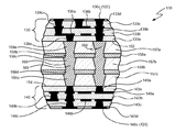
次に図1A及び1Bを参照するに、2つ以上のガラス層を有するコア150を含む基板100の実施形態が示されている。図1Aは基板100の平面図を示し、図1Bは、図1Aの直線B−Bに沿って取られた基板の立断面図を示している。また、多層ガラスコアを有する基板100の様々な選択的な実施形態を図1C乃至1Gに示す。図1C乃至1Gの各々は、図1Bで参照符号5によって大まかに特定される基板100の一部を拡大図にて示している。
Referring now to FIGS. 1A and 1B, an embodiment of a
図1A及び1Bを参照するに、基板100は、多数のガラス層157a、157b及び157cを有するコア150を含んでいる。一実施形態において、コア150は更に、ガラス層157a、157b、157cの間に配置された接合層158a及び158bを含む(例えば、層158aがガラス層157aと157bとの間に配置され、等々)。基板100は、第1の面102と、それとは反対側の、第1の面102と概して平行な第2の面104とを有する。基板100の周縁108が第1の面102と第2の面104との間に延在している。一部の実施形態によれば、基板100の周縁108は概して長方形であり、一実施形態において、周縁108の4つ全ての側面は、周縁が正方形を形成するように実質的に相等しい。しかしながら、長方形ではない周縁を有する基板も開示の実施形態の範囲内である。一実施形態において、基板100は0.2mmと1.1mmとの間の厚さを有する。
Referring to FIGS. 1A and 1B, the
多層ガラスコア150は、第1表面152と、それとは反対側の第2表面154とを有する。一実施形態において、第1表面152及び第2表面154は互いに概して平行である。ガラスコア150の周縁158が第1表面152と第2表面154との間に延在しており、一部の実施形態において、ガラスコアの周縁158は基板の周縁108と概して一致する。一実施形態によれば、多層ガラスコア150は50μmと800μmとの間の厚さを有し得る。個々のガラス層157a、157b、157cは好適な如何なる種類のガラスを有していてもよい。一実施形態において、ガラス層157a−157cは同じガラス材料を有するが、他の実施形態において、ガラス層157a−157cのうちの何れかが、その他のガラス層のうちの何れかのガラス材料とは異なるガラス材料を有していてもよい。
The
多数の導電体160が多層ガラスコア150内を延在している。各導電体160は孔(ホール)又はビア165内に配置され、各導電体160が第1表面152から第2表面154まで延在し得る。しかしながら、他の実施形態においては、導電体のうちの1つ以上がコア厚さ内を部分的にのみ延在する。一実施形態によれば、導電体160は、導電材料で充填された、コア150を貫いて形成された孔又はビア165を有する。
A number of
導電体160は、金属、複合材料及び導電性ポリマーを含む好適な如何なる導電材料を有していてもよい。好適な金属は、銅、錫、銀、金、ニッケル、アルミニウム及びタングステン、並びにこれら及び/又はその他の金属の合金を含む。孔又はビア165を形成するために使用され得るプロセスは、例えば、エッチング、レーザドリル加工、インプリント、及びサンドブラスティングを含む。導電体160を形成するように、孔又はビア165内に、例えばめっき技術(電解めっき又は無電解めっき)、化学気相成長(CVD)、物理気相堆積(PVD)若しくはスクリーン印刷技術、及びこれら及び/又はその他のプロセスの組み合わせなどの好適プロセスによって、導電材料が堆積され得る。孔165の形成及び導電体160の形成の様々な実施形態については更に詳細に後述する。
The
基板100の第1の面102上に、第1組の導電端子120(図1A参照)が配設される。一実施形態によれば、第1組の端子120は、集積回路(IC)ダイ上に配設された対応する端子アレイと結合するパターンで配列される。図1A−1BはICダイを示していないが、図1Aはダイ領域110を示しており、端子120はこのダイ領域(ダイシャドウ領域と呼ぶこともある)内にある。端子120は各々、ICダイの端子との電気接続を形成することが可能な如何なる好適種類の構造を有していてもよい。例えば、端子120は、好適な金属又は複数の金属の組み合わせから形成されたパッド、ピラー又はスタッドバンプを有することができ、各端子120上(及び/又はICダイの端子上)にはんだバンプが配設され得る。一実施形態において、ICダイはフリップチップ法で基板100上に配置され、はんだリフロープロセスによって、ダイ上の端子が基板100上の端子120と結合される。他の一実施形態によれば、ICダイは接着剤の層によって基板100に結合され、ワイヤボンドプロセスによって、ダイ上の端子が基板上の対応する端子に電気的に結合され得る(この実施形態において、端子120はダイ領域110の外側にある)。
A first set of conductive terminals 120 (see FIG. 1A) is disposed on the
基板100の第2の面104上に、第2組の導電端子125(図示の明瞭性及び便宜のため、図1Aには一部のみを示す)が配設される。一実施形態によれば、第2組の端子125は、例えばメインボード、マザーボード又はその他の回路基板などの次階層の部品(図示せず)上に配設された対応する端子アレイと結合するパターンで配列される。端子125は各々、次階層部品の端子との電気接続を形成することが可能な如何なる好適種類の構造を有していてもよい。例として、端子125は、パッド、ランド、はんだバンプ若しくはその他の金属バンプ、又はピンを有し得る。次階層部品は、例えばランドグリッドアレイ(LGA)ソケット又はピングリッドアレイ(PGA)ソケットなど、基板100及び端子125を受け入れるためのソケット(及び保持機構)を含み得る。他の例では、端子125は、はんだリフロープロセスによって次階層部品の端子と結合されてもよい。
A second set of conductive terminals 125 (only a portion of which is shown in FIG. 1A for clarity and convenience of illustration) is disposed on the
コア150の第1表面152上に第1のビルドアップ構造130が配設され、コアの第2表面154上に第2のビルドアップ構造140が配設される。第1のビルドアップ構造は、誘電体材料及び金属の1つ以上の交互層を有し、端子120は該第1のビルドアップ構造130上に配置される(第1の基板面102は一般に第1のビルドアップ構造130の外表面に相当する)。多層ガラスコア150内の導電体160のうちの少なくとも1つが、第1のビルドアップ構造130の少なくとも1つの金属層と電気的に結合され、一実施形態において、第1のビルドアップ構造の、コア150に最も近い金属層が、少なくとも1つの導電体160と結合される。同様に、第2のビルドアップ構造140は、誘電体材料及び金属の1つ以上の交互層を有し、端子125は該第2のビルドアップ構造140上に配置される(第2の基板面104は一般に第2のビルドアップ構造140の外表面に相当する)。コア150内の導電体160のうちの少なくとも1つが、第2のビルドアップ構造140の少なくとも1つの金属層と電気的に結合され、一実施形態において、第2のビルドアップ構造の、コア150に最も近い金属層が、少なくとも1つの導電体160と結合される。第1及び第2のビルドアップ構造130、140は、第1組の端子120と第2組の端子125との間で、電力と入力/出力(I/O)信号とをルーティングする(ひいては、基板100上に搭載されたICダイと次階層部品との間での電力送達及び信号伝達を支援する)。ビルドアップ構造130、140については更に詳細に後述する。
A
図1Cを参照するに、多層ガラスコア基板100の一実施形態が更に詳細に示されている。上述のように、この基板は、ガラス層157a、157b及び157cを有するコア150を含んでおり、コアは第1表面152とそれと反対側の第2表面154とを有している。上述のように、ガラス層157a−157cの間に接合層158a、158bが配置されている。図1A乃至1Gには3つのガラス層が示されているが、コア150は、基板100の所望の機械特性及び電気特性に応じて、如何なる好適数(例えば、2層、4層以上など)のガラス層を有していてもよい。ガラス層157a−157cは好適な如何なる厚さを有していてもよく、一実施形態において、各ガラス層はおよそ50μmと200μmとの間の厚さを有する。また、一実施形態において、ガラス層157a−157cは、(図示のように)全てが同じ厚さを有していてもよいし、それに代えて、ガラス層157a−157cのうちの何れか1つがその他のガラス層のうちの1つ以上とは異なる厚さを有していてもよい。接合層158a−158bもまた、好適な如何なる厚さを有していてもよく、一実施形態において、各接合層はおよそ20μmと100μmとの間の厚さを有する。一実施形態によれば、接合層158a−158bは、(図示のように)全てが同じ厚さを有する。しかしながら、他の実施形態においては、接合層158a−158bのうちの何れか1つがその他の接合層のうちの1つ以上とは異なる厚さを有し得る。
Referring to FIG. 1C, one embodiment of a multilayer
別個のガラス層157a、157b、157cは、如何なる好適技術によってともに接合されてもよい。一実施形態において、接合層158a、158bがガラス層間に配置され、これら接合層の各々が2つの隣接するガラス層と結合される(例えば、接合層158aがガラス層157a及び157bと結合され、等々)。一実施形態によれば、各接合層158a、158bは接着剤を含み、更なる一実施形態において、接合層158a、158bは有機材料を有する。一実施形態によれば、各接合層158a、158bは、例えばアクリル樹脂又はエポキシ樹脂を有するフィルムなどのドライフィルム接着材を有する。しかしながら、理解されるべきことには、開示の実施形態は接着接合に限定されず、また、多層ガラスコア150は接着剤を用いずに形成されてもよい。一部の実施形態において、ガラス層157a−157cは拡散接合によってともに結合され得る。例えば、一実施形態において、接合層158a−158bは、層157a−157cのガラス材料と拡散結合を形成することが可能な材料を有する(例えば、接合層158aがガラス層157a及び157bの各々と拡散結合を形成し、等々)。他の例では、ガラス層157a−157cが互いに直接的に拡散結合されてもよく(例えば、ガラス層157aがガラス層157bと拡散結合され、等々)、その場合、接合層158a−158bは省略され得る。他の実施形態において、ガラス層157a−157cは機械的に接合され得る。例として、一実施形態において、スルーホール165内に堆積された導電材料160が、ガラス層157a−157cをともに固定するよう機能し得る。更なる一実施形態において、ガラス層157a−157cは直接酸化物間接合を用いてともに固定されてもよい。
The
一実施形態によれば、第1のビルドアップ構造130は、多数の誘電体層133a、133b、133c、133dと、多数の金属層136a、136b、136cを有する。誘電体層133a−133dは好適な如何なる誘電体材料(例えば、ポリマー材料など)を有していてもよく、また、好適な如何なる技術(例えば、堆積、ラミネーションなど)によって形成されてもよい。金属層136a−136cは好適な如何なる導電材料(例えば、銅、アルミニウム、銀など)を有していてもよく、また、好適な如何なる技術(例えば、電解めっき又は無電解めっきなどのめっきプロセス)によって堆積されてもよい。また、金属層136a−136cは各々、電力及びI/O信号のルーティングを容易にするのに好適な数及び構成の配線、電源プレーン、グランドプレーン、及びその他の導電体を形成するようにパターニングされ得る。
According to one embodiment, the
如何なる2つの隣接する金属層136a−136cの間にも誘電体層133a−133dのうちの1つが配置され(例えば、金属層136aと136bとが誘電体層133bによって離隔され、等々)、誘電体層133aはコア150に隣接し、金属層136aをコアから離隔している。一実施形態によれば、誘電体層133aはコアの第1表面152に直接的に接触する。金属でめっきあるいは充填されたビア139a、139b、139cが、それぞれ、誘電体層133a、133b、133cを貫通して延在し、隣接し合う金属層を相互接続する(例えば、ビア139bが金属層136aと金属層136bとを相互接続し、等々)。また、多層ガラスコア150に最も近い金属層136aは、誘電体層133a内に配設されたビア139aによって、導電体160のうちの1つ以上と結合される。一実施形態において、コア150の第1表面152は、ビルドアップ構造130の誘電体材料との密着性を高めるための表面処理又はコーティングを含んでいてもよい。また、一部の実施形態において、最も外側の誘電体層133dはレジスト層及び/又はパッシベーション層を有し得る。また、一実施形態によれば、最も外側の金属層136cによって、あるいはその上に、端子120が形成される。
One of the
一実施形態において、第2のビルドアップ構造140は、多数の誘電体層143a、143b、143c、143dと、多数の金属層146a、146b、146cを有する。誘電体層143a−143dは好適な如何なる誘電体材料(例えば、ポリマー材料など)を有していてもよく、また、好適な如何なる技術(例えば、堆積、ラミネーションなど)によって形成されてもよい。金属層146a−146cは好適な如何なる導電材料(例えば、銅、アルミニウム、銀など)を有していてもよく、また、好適な如何なる技術(例えば、電解めっき又は無電解めっきなどのめっきプロセス)によって堆積されてもよい。また、金属層146a−146cは各々、電力及びI/O信号のルーティングを容易にするのに好適な数及び構成の配線、電源プレーン、グランドプレーン、及びその他の導電体を形成するようにパターニングされ得る。
In one embodiment, the second build-up
如何なる2つの隣接する金属層146a−146cの間にも誘電体層143a−143dのうちの1つが配置され(例えば、金属層146aと146bとが誘電体層143bによって離隔され、等々)、誘電体層143aはコア150に隣接し、金属層146aをコアから離隔している。一実施形態によれば、誘電体層143aはコアの第2表面154に直接的に接触する。金属でめっきあるいは充填されたビア149a、149b、149cが、それぞれ、誘電体層143a、143b、143cを貫通して延在し、隣接し合う金属層を相互接続する(例えば、ビア149bが金属層146aと金属層146bとを相互接続し、等々)。また、多層ガラスコア150に最も近い金属層146aは、誘電体層143a内に配設されたビア149aによって、導電体160のうちの1つ以上と結合される。一実施形態において、コア150の第2表面154は、ビルドアップ構造140の誘電体材料との密着性を高めるための表面処理又はコーティングを含んでいてもよい。また、一部の実施形態において、最も外側の誘電体層143dはレジスト層及び/又はパッシベーション層を有し得る。また、一実施形態によれば、最も外側の金属層146cによって、あるいはその上に、端子125が形成される。
One of the
図1Cの実施形態(並びに、図1D及び1Gの各々に示す実施形態)においては、第1及び第2のビルドアップ構造は、相等しい数の誘電体層及び金属層を有するとともに、概して相等しい厚さを有している。しかしながら、開示の実施形態はそのように限定されず、他の実施形態においては、第1及び第2のビルドアップ構造は、相異なる厚さ、及び/又は相異なる数の誘電体層及び金属層を有していてもよい。他の一実施形態によれば、ビルドアップ構造は多層ガラスコア150の一方側のみに配設される。また、一部の実施形態において、第1及び第2のビルドアップ構造は同じ誘電体材料及び金属から構築される。しかしながら、他の実施形態においては、第1及び第2のビルドアップ構造は相異なる材料を有していてもよい。
In the embodiment of FIG. 1C (and the embodiment shown in each of FIGS. 1D and 1G), the first and second build-up structures have equal numbers of dielectric and metal layers and are generally equal. It has a thickness. However, the disclosed embodiments are not so limited, and in other embodiments, the first and second build-up structures may have different thicknesses and / or different numbers of dielectric and metal layers. You may have. According to another embodiment, the build-up structure is disposed only on one side of the
図1Cの実施形態においては、誘電体層133a及び143aが多層ガラスコア150に隣接して位置し、コアに最も近い金属層(すなわち、金属層136a及び146a)がこれらの誘電体層によってコアから離隔されている。これに代わる一実施形態においては、図1Dに示すように、多層ガラスコア150に金属層が隣接してもよい。コア150の片側又は両側に隣接して金属層を組み込むことは、“コア層ルーティング”と呼ばれることもある。
In the embodiment of FIG. 1C,
図1Dを参照するに、この実施形態に係る基板100は、図1Cに示したものと概して同様である(同様の部分は同じ参照符号によって識別している)。しかしながら、図1Dの実施形態においては、第1のビルドアップ構造130が、多層ガラスコア150に隣接する金属層136xを含んでおり、一実施形態によれば、金属層136xはコアの第1表面152に直に接触する。誘電体層133aは金属層136x(及びコアの露出部分)の上に位置しており、ここでは、コアに最も近い金属層はこの金属層136xであり、導電体160のうちの少なくとも1つが金属層136xに結合される。また、他の一実施形態において、コア150の第1表面152は、金属層136x(及び、恐らくは、誘電体層133aの部分群)との密着性を高めるための表面処理又はコーティングを含み得る。
Referring to FIG. 1D, the
第1のビルドアップ構造130と同様に、図1Dの第2のビルドアップ構造140は、多層ガラスコア150に隣接する金属層146xを含んでおり、一実施形態において、金属層146xはコアの第2表面154に直に接触する。誘電体層143aは金属層146x(及びガラスコアの露出部分)の上に位置しており、ここでは、コアに最も近い金属層はこの金属層146xであり、導電体160のうちの少なくとも1つが金属層146xに結合される。また、他の一実施形態において、コア150の第2表面154は、金属層146x(及び、恐らくは、誘電体層143aの部分群)との密着性を高めるための表面処理又はコーティングを含み得る。一部の実施形態において、コアの両側の表面152、154のうちの一方のみが隣接する金属層を有する(例えば、第1及び第2のビルドアップ構造130、140それぞれの金属層136x、146xのうちの何れか一方が省略され得る)。
Similar to the
図1Eを参照するに、更なる一実施形態に係る多層ガラスコア基板100が示されている。図1Eに示す実施形態に係る基板100は、図1Cに示したものと概して同様である(同様の部分は同じ参照符号によって識別している)。しかしながら、図1Eの実施形態においては、その中に各導電体160が配置される孔又はビア165は、コア150の厚さにわたって傾斜を有するテーパー壁を有している。一実施形態において、孔又はビア165のテーパー壁は、該孔の中心線に対して0と45°との間の角度167を有する。孔165のテーパー壁は、多層ガラスコア150を貫通する孔を形成するために使用されるプロセスの結果であり得る。上述のように、孔又はビア165を形成するために使用され得るプロセスは、例えば、エッチング、レーザドリル加工、インプリント、及びサンドブラスティングを含む。処理条件に応じて、上述の技術のうちの何れか1つが、テーパー壁を有する孔165を形成し得る。理解されるように、形成技術及びプロセス条件に応じて、ビアは、図1Eに描かれた直線状のテーパー壁以外の形状を有し得る。例えば、他の実施形態において、ビアの壁は曲線状となり得る(例えば、ビアは扇形の断面形状を有し得る)。
Referring to FIG. 1E, a multilayer
次に、図1Fを参照するに、更なる一実施形態に係る多層ガラスコア基板100が示されている。図1Fに示す実施形態に係る基板100は、図1Cに示したものと概して同様である(同様の部分は同じ参照符号によって識別している)。しかしながら、図1Fの実施形態においては、その中に各導電体160が配置される孔又はビア165は、別個のガラス層157a、157b、157c、及び接合層158a、158bの各々に形成された多数の別々の整列された孔を有している。例えば、スルーホール165は、ガラス層157a内のビア159aと、接合層158a内のビア159bと、ガラス層157b内のビア159cと、接合層158b内のビア159dと、ガラス層157c内のビア159eとを有し得る。一般に、これら別々の孔159a−159eは共通の中心線に沿ってアライメントされるが、一部の実施形態において、これら別々の孔の間にミスアライメントが存在し得る。
Referring now to FIG. 1F, a multilayer
一実施形態によれば、ガラス層内に形成されるビア(例えば、ビア159a、159c、159e、及び場合により接合層158a、158b)は、そのガラス層(又は接合層)の厚さにわたって傾斜されたテーパー壁を有し得る。一実施形態において、1つのビアのテーパー壁は、その孔の中心線に対して0と45°との間の角度169を有する。ビア(例えば、ビア159a−159e)のテーパー壁は、形成プロセスの結果であり得る。上述のように、ガラス層を貫通する(及び接合層を貫通する)ビアを形成するために使用され得るプロセスは、例えば、エッチング、レーザドリル加工、インプリント、及びサンドブラスティングを含む。処理条件に応じて、上述の技術のうちの何れか1つが、テーパー壁を有するビアを形成し得る。理解されるように、形成技術及びプロセス条件に応じて、ビアは、図1Fに描かれた直線状のテーパー壁以外の形状を有し得る。他の実施形態において、ビアの壁は曲線状となり得る。例えば、ビアは扇形の断面形状を有し得る(例えば、図8Jを参照)。
According to one embodiment, vias formed in a glass layer (eg, vias 159a, 159c, 159e, and optionally bonding
次に、図1Gを参照するに、更なる一実施形態に係る多層ガラスコア基板100が示されている。図1Gに示す実施形態に係る基板100は、図1Cに示したものと概して同様である(同様の部分は同じ参照符号によって識別している)。しかしながら、図1Gの実施形態においては、接合層158a、158bのうちの何れか1つ以上が導電体を含み得る。例えば、接合層158aは導電体198aを含むことができ、接合層158bは導電体198bを含むことができる。導電体198a、198bは、I/O信号をルーティングするための配線、及び/又は電力をルーティングするための配線を有し得る。また、接合層158a、158bのうちの何れか1つ以上の導電体198a、198bは、電源プレーン又はグランドプレーンを有していてもよい。導電体198a、198bは、例えば金属(例えば、銅、ニッケル、アルミニウム、銀、金、並びにこれら及び/又はその他の金属の合金)、導電性ポリマー又は複合材料などの好適な如何なる導電材料を有していてもよい。また、図1Gにおいては接合層158a、158bの双方が導電体を含んでいるが、他の実施形態においては、一部の接合層のみが導電体を含んでいてもよい。
Referring now to FIG. 1G, a multilayer
図2は、多層ガラスコア基板100を含んだアセンブリ(組立体)200の一実施形態を示している。図2を参照するに、アセンブリ200は、多層ガラスコア150と第1の面102及び反対側の第2の面104とを有する基板100を含んでいる。基板の第1の面102上に、集積回路(IC)ダイ210が配置されている。ICダイ210は、多数のインターコネクト220によって、基板100と電気的(且つ機械的)に結合されている。基板の第2の面104上の端子125(例えば、ランド、ピン、はんだバンプなど)(図1A参照)が、例えばマザーボード、メインボード又はその他の回路基板などの次階層部品との電気接続を形成するために使用され得る。第1表面232と、それと反対側の、ダイの裏面215に面する第2表面234と、を有するヒートスプレッダ又は蓋230が、ダイ210上に配設され、サーマルインタフェース(熱接続)材料の層240を介してダイの裏面215と熱的(恐らくは、且つ機械的に)に結合される。ガラスコア基板100の第1の面102にヒートスプレッダ230を固定するために、接着剤又は封止材290が使用され得る。図2には示していないが、更なる一実施形態において、ヒートシンク(又はその他の冷却装置)がヒートスプレッダ230と熱的に結合され、ヒートスプレッダの第1表面232とヒートシンク(又はその他の装置)との間に別のサーマルインタフェース材料層が配置されてもよい。
FIG. 2 illustrates one embodiment of an
ICダイ210は如何なる種類の半導体デバイスを有していてもよい。一実施形態において、ICダイ210は演算処理用のシステム又はデバイスを有する。例えば、ICダイ210はマイクロプロセッサ又はグラフィックプロセッサを有し得る。ICダイ210は、任意数の命令フォーマットを有する任意数のプロセッサアーキテクチャからの命令を実行することができる。一実施形態において、命令は、インテル社によって使用されているような“x86”命令である。しかしながら、他の実施形態において、プロセッサは、その他のアーキテクチャ又はその他のプロセッサ設計者からの命令を実行してもよい。他の一実施形態において、ICダイ210はメモリデバイスを有する。更なる一実施形態によれば、ICダイ210はシステム・オン・チップ(SoC)を有する。更なる他の一実施形態において、ICダイ210は、デジタル回路、アナログ回路、又はアナログ回路及びデジタル回路双方の組み合わせを含んでいてもよい。 IC die 210 may have any type of semiconductor device. In one embodiment, the IC die 210 has a system or device for arithmetic processing. For example, IC die 210 may have a microprocessor or graphics processor. IC die 210 can execute instructions from any number of processor architectures having any number of instruction formats. In one embodiment, the instruction is an “x86” instruction as used by Intel. However, in other embodiments, the processor may execute instructions from other architectures or other processor designers. In another embodiment, the IC die 210 has a memory device. According to a further embodiment, the IC die 210 has a system on chip (SoC). In yet another embodiment, the IC die 210 may include a digital circuit, an analog circuit, or a combination of both analog and digital circuits.
インターコネクト220は、例えばはんだリフロープロセスにより、基板の第1の面102上の端子120(図1A参照)をICダイ210上の端子と結合することによって形成される。上述のように、基板端子120は各々、好適な金属又は複数の金属の組み合わせ(例えば、銅、ニッケル、アルミニウムなど)から形成されたパッド、ピラー又はスタッドバンプを有することができ、ダイ端子もまた、好適な金属又は複数の金属の組み合わせから形成されたパッド、ピラー又はスタッドバンプを有し得る。基板端子及び/又はダイ端子の上に(例えば、ボール又はバンプの形態をした)はんだが配置され、そして、はんだリフロープロセスを用いてこれらの端子が結合される。理解されるように、上述のインターコネクトは、基板100とICダイ210との間に形成されることが可能なインターコネクト種類のうちの単なる一例であり、その他の好適種類のインターコネクトが使用されてもよい。また、インターコネクト220の周り、及びICダイ210と基板の第1の面102との間に、アンダーフィル材料の層(図2には図示せず)が配設されてもよい。
The
ヒートスプレッダ230は、好適な如何なる熱伝導材料を有していてもよく、また、好適な如何なる形状又は構造を有していてもよい。一実施形態によれば、ヒートスプレッダ230は、基板の第1の面102に向かって延在する側壁(又は複数の側壁)237を含む蓋を有し、この側壁(又は複数の側壁)が接着剤290によって基板表面102に固定される。上述の蓋は一体化ヒートスプレッダ(integrated heat spreader;IHS)と呼ばれるときもある。ヒートスプレッダ230を構築するために使用され得る材料は、金属(例えば、銅及びその合金)、熱伝導性コンポジット及び熱伝導性ポリマーを含む。
The
図2に示した実施形態において、アセンブリ200は単一のICダイ210を含んでいる。しかしながら、他の実施形態において、アセンブリ200はマルチチップパッケージを有していてもよい。例えば、1つ以上のその他の集積回路ダイ(例えば、メモリデバイス、電圧調整器など)が基板100上に配置され得る。さらに、例えばキャパシタ及びインダクタなどの受動デバイスが、ガラスコア基板100上に配置されたり、あるいは基板のビルドアップ構造130、140に集積されたりしてもよい。例として、アレイキャパシタ又は薄膜キャパシタが、基板のビルドアップ構造130、140に集積され得る。他の一実施形態において、例えばアンテナ又はRFシールドなどの無線部品が、ガラスコア基板100上に配置されたり、あるいは該基板のビルドアップ構造130、140に集積されたりしてもよい。これらの追加デバイスは、ICダイ、受動デバイス又はその他の部品の何れであろうと、ガラスコア基板100の何れかの側102、104に配置され得る。
In the embodiment shown in FIG. 2, the
アセンブリ200は、如何なる種類の計算装置の一部を形成してもよい。一実施形態によれば、アセンブリ200はサーバ又はデスクトップコンピュータの一部を形成し得る。他の一実施形態において、アセンブリ200はラップトップコンピュータ又は同様の移動計算装置(例えば、ネットトップコンピュータ)の一部を形成する。更なる一実施形態において、アセンブリ200は、例えばセル方式電話、スマートフォン又はモバイルインターネット装置(MID)などの手持ち式計算装置の一部を有する。更なる他の一実施形態において、アセンブリ200は埋込計算装置の一部を形成する。
The
図3は、多層ガラスコア基板を製造する方法の一実施形態を示している。図3の方法は更に図4A−4Cに示されており、以下の説明では、これらの図を参照する。 FIG. 3 illustrates one embodiment of a method for manufacturing a multilayer glass core substrate. The method of FIG. 3 is further illustrated in FIGS. 4A-4C and will be referred to in the following description.
図3のブロック310を参照するに、一実施形態において、1つ以上のスルーホールを有する多層ガラスコアが準備される。これは、コア450を示す図4Aに例示されている。多層ガラスコア450は、図1A乃至1Gに示して説明したコア150の実施形態の何れを有していてもよい。多層ガラスコア450は、接合層458a、458bによってともに固定された別々のガラス層457a、457b、457cを含んでおり、該コアは、第1表面452と、それと反対側の、第1表面452と概して平行な第2表面454とを有している。孔又はビア465が第1表面452から第2表面454まで延在している。コア450のガラス層457a−457cは、用途及び/又は所望特性に応じて、如何なる好適種類のガラスを有していてもよく、また、好適な如何なる厚さ(上述の説明を参照)を有していてもよい。一実施形態によれば、コア450は、単一の基板の形成を可能にするサイズ及び構成を有する。更なる一実施形態において、コア450は、2つ以上の基板の形成を可能にするサイズ及び構成を有する(例えば、コア450は、2つ以上の基板が切り出されるパネルを有する)。1つ以上のスルーホールを有する例えばコア450などの多層ガラスコアを形成する方法の様々な実施形態を、図5、7、9及び11の各々に示す。それらの実施形態については更に詳細に後述する。
Referring to block 310 of FIG. 3, in one embodiment, a multi-layer glass core having one or more through holes is provided. This is illustrated in FIG. 4A showing the
ブロック320を参照するに、スルーホール内に導電材料が配置され、導電体が形成される。これは図4Bに例示されており、そこでは、導電材料が孔465内に配置されて導電体460を形成している。
Referring to block 320, a conductive material is disposed in the through hole to form a conductor. This is illustrated in FIG. 4B where a conductive material is disposed within the
導電材料460はビア465内に、例えばめっき技術(電解めっき若しくは無電解めっき)、CVD、PVD若しくはスクリーン印刷技術、及びこれら及び/又はその他のプロセスの組み合わせなどの好適プロセスによって堆積され得る。コア450内の導電体460を形成する材料は、金属、複合材料及び導電性ポリマーを含む好適な如何なる導電材料を有していてもよい。好適な金属は、銅、錫、銀、金、ニッケル、アルミニウム及びタングステン、並びにこれら及び/又はその他の金属の合金を含む。
多層ガラスコアのスルーホール内に導電体を形成する方法の一実施形態を図13に示し、今からそれを説明する。図13の方法の実施形態は更に図14A−14Cの模式図に示されており、以下の説明では、図13及び14A−14Cを参照する。 One embodiment of a method for forming a conductor in a through hole of a multilayer glass core is shown in FIG. 13 and will now be described. The embodiment of the method of FIG. 13 is further illustrated in the schematic diagrams of FIGS. 14A-14C, and the following discussion refers to FIGS. 13 and 14A-14C.
図13のブロック1305を参照するに、多層ガラスコア内のスルーホールの壁にシード層又は接着層が堆積される。これは更に、コア1450を示す図14Aに示されている。コア1450は、接合層1458a、1458b、1458cによってともに結合されたガラス層1457a、1457b、1457c、1457dを有している(例えば、接合層1458aがガラス層1457a及び1457bの双方に結合され、等々)。スルーホール1465が、コアの第1表面1452から、それと反対側のコアの第2表面1454まで、コア1450を貫いて延在している。孔1465は、例えばエッチング、レーザドリル加工、インプリント、及びサンドブラスティングなどの好適な方法又は複数の方法の組み合わせによって形成され得る。スルーホール1465の壁にシード層1466が堆積される。なお、他の実施形態において、シード層1466に先立って、1つ以上のその他の材料層が堆積されてもよい。例えば、シード層1466の堆積に先立って、スルービア1465の壁に誘電体層が堆積され得る(例えば所望のキャパシタンスを達成するため、所望の電気絶縁を達成するため、等々)。
Referring to block 1305 of FIG. 13, a seed layer or adhesive layer is deposited on the walls of the through holes in the multilayer glass core. This is further illustrated in FIG. 14A showing the
シード層1466の上には、後続の金属層が堆積されることになる。シード層は1466、層1457a−1457dのガラス材料(及び接合層1458a−1458cの材料)と、続いて堆積される金属層とに接着することが可能な如何なる材料を有していてもよい。好適なシード層材料は、銅、チタン、クロム、ニッケル若しくはバナジウム、及びこれら及び/又はその他の金属の合金を含む。また、シード層1466は、無電解めっき、電解めっき、CVD又はPVDを含む好適な如何なる技術を用いて堆積されてもよい。一実施形態において、ブランケット(全面)堆積技術が用いられ、シード層1466は、図14Aに示すように、コア1450の第1及び第2の表面1452、1454上にも延在し得る。シード層1466は好適な如何なる厚さを有していてもよく、一実施形態において、この層は0.1μmと0.5μmとの間の厚さを有する。
Subsequent metal layers will be deposited on the
ブロック1315にて説明するように、シード層上に金属が配設される。これは図14Bに示されており、そこでは、金属層1467がシード層1466上に配設されている。金属層1467は、銅、アルミニウム、ニッケル、銀若しくは金、及びこれら及び/又はその他の金属の合金などの好適な如何なる導電性金属を有していてもよい。金属層1467は、無電解めっき、電解めっき、CVD又はPVDを含む好適な如何なる技術を用いて堆積されてもよい。一実施形態において、ブランケット堆積技術が用いられ、金属層1467は、図14Bに示すように、コア1450の第1及び第2の表面1452、1454上にも延在し得る。金属層1467は好適な如何なる厚さを有していてもよく、一実施形態において、この層は5μmと30μmとの間の厚さを有する。他の一実施形態において、シード層1466上に堆積される金属1467はスルーホール1465を実質的に充填する。
Metal is disposed on the seed layer as described in
次に、ブロック1325を参照するに、スルーホールを充填するように、金属層上に誘電体材料が配設される。これは図14Cに示されており、そこでは、各孔1465の内部の空隙を充填するように、誘電体材料1468が金属層1467上に配設されている。誘電体材料1468は好適な如何なる材料を有していてもよく、一実施形態において、誘電体材料1468は有機材料を有する。また、誘電体材料1468は、例えばスクリーン印刷、CVD又はPVDなどの好適な如何なる技術を用いて堆積されてもよい。しかしながら、やはり、金属層1467がスルーホール1465を実質的に充填してもよく、その場合、誘電体材料は省略され得る。更なる一実施形態において、図14Cに示すように、余分なシード層1466及び余分な金属層1467が、コア1450の第1及び第2の表面1452、1454から除去され得る。余分なシード層及び金属層は、例えば、研削プロセス、化学的機械的研磨技術又はエッチングプロセスによって表面1452、1454から除去され得る。
Next, referring to block 1325, a dielectric material is disposed on the metal layer to fill the through holes. This is shown in FIG. 14C where a
続いて、図3、具体的にはブロック330に戻るに、上述のビルドアップ構造を作り出すために、1つ以上のビルドアップ層が多層ガラスコアの各面(又は、場合により、一方の面のみ)に配設される。これは図4Cに示されており、そこでは、第1のビルドアップ構造430がコア450の第1表面452上に形成され、第2のビルドアップ構造440がコアの第2表面454上に形成されている。各ビルドアップ構造430、440は、誘電体材料及び金属の如何なる好適数(例えば、1つ又は複数)の交互層を有していてもよく、それらは好適な如何なる技術によって形成されてもよい。このようなビルドアップ構造の構造及び形成法については、図1B乃至1Gを参照した上述の説明にて更に詳細に説明されている。一実施形態において、導電体460のうちの少なくとも1つが、第1のビルドアップ構造430の、コア450に最も近い金属層と電気的に結合され、更なる一実施形態において、導電体460のうちの少なくとも1つが、第2のビルドアップ構造440のコアに最も近い金属層と電気的に結合される。多層ガラスコア450とビルドアップ構造430、440との組み合わせは、集積回路デバイス用の基板400を有し得る。
Subsequently, returning to FIG. 3, specifically block 330, one or more build-up layers are formed on each side of the multilayer glass core (or, in some cases, only one side, to create the build-up structure described above. ). This is shown in FIG. 4C, where a
次に、図3のブロック340を参照するに、基板上に導電端子が形成され得る(図4A−4Cには端子は示していない)。第1組の端子が第1のビルドアップ構造430上に形成され、第2組の端子が第2のビルドアップ構造440上に形成され得る。このような端子の構造及び形成法については、図1A乃至1Gを参照した上述の説明にて更に詳細に説明されている。
Next, referring to block 340 of FIG. 3, conductive terminals may be formed on the substrate (terminals are not shown in FIGS. 4A-4C). A first set of terminals may be formed on the
上述のように、一実施形態において、多層ガラスコア450、並びに第1及び第2のビルドアップ構造430、440は、2つ以上の基板に対応する構造及び機能を含む。この実施形態において、コア450(ビルドアップ構造430、440を備える)は、(端子の形成の前又は後の何れかで)それら別個の基板へと個片化されることになる。
As described above, in one embodiment, the
続いて、図5を参照するに、1つ以上のスルーホールを有する多層ガラスコアを形成する方法の一実施形態が示されている。図5に示す方法は更に図6A−6Cの模式図に示されており、以下の説明では、これらの図を参照する。 Continuing with reference to FIG. 5, one embodiment of a method of forming a multilayer glass core having one or more through-holes is shown. The method shown in FIG. 5 is further illustrated in the schematic diagrams of FIGS. 6A-6C, and will be referred to in the following description.
図5のブロック510を参照するに、多層ガラス板が準備される。これは、多層ガラス板605を示す図6Aに例示されている。板605は、接合層658a、658b、658cによってともに貼り付けられた多数のガラス層657a、657b、657c、657dを有している(例えば、接合層658aがガラス層657a及び657bと結合され、等々)。多層ガラス板605はまた、第1表面652と第2表面654との間に延在する周縁651を有する。一実施形態によれば、多層ガラス板605は50μmと800μmとの間の厚さを有し得る。一実施形態において、多層ガラス板は、単一の基板コアの形成を可能にするサイズ及び構成を有する。更なる一実施形態において、板605は、2つ以上の基板コアの形成を可能にするサイズ及び構成を有する(例えば、板605は、2つ以上の基板コア、すなわち、2つ以上の基板が切り出されることになるパネルを有する)。
Referring to block 510 of FIG. 5, a multi-layer glass plate is prepared. This is illustrated in FIG. 6A showing a
個々のガラス層657a−657dは、如何なる好適種類のガラスを有していてもよい。一実施形態において、ガラス層657a−657dは同じガラス材料を有する。しかしながら、他の実施形態においては、ガラス層657a−657dのうちの何れか1つが、その他のガラス層のうちの何れかのガラス材料とは異なるガラス材料を有していてもよい。図6A−6Cには4つのガラス層が示されているが、板605は、板605から形成されるコア(又は、複数のコア)の所望の機械特性及び電気特性に応じて、如何なる好適数のガラス層(例えば、二層、三層、5層以上など)を有していてもよい。ガラス層657a−657dは好適な如何なる厚さを有していてもよく、一実施形態において、各ガラス層はおよそ50μmから200μmの厚さを有する。また、一実施形態において、ガラス層657a−657dは、(図示のように)全てが同じ厚さを有していてもよいし、それに代えて、ガラス層657a−657dのうちの何れか1つがその他のガラス層のうちの1つ以上とは異なる厚さを有していてもよい。
The
接合層658a−658cもまた、好適な如何なる厚さを有していてもよく、一実施形態において、各接合層はおよそ20μmから100μmの厚さを有する。一実施形態によれば、接合層658a−658cは、(図示のように)全てが同じ厚さを有する。しかしながら、他の実施形態においては、接合層658a−658cのうちの何れか1つがその他の接合層のうちの1つ以上とは異なる厚さを有し得る。
The
別個のガラス層657a、657b、657c、657dは、如何なる好適技術によってともに接合されてもよい。一実施形態において、図示のように、接合層658a、658b、658cがガラス層間に配置され、これら接合層の各々が2つの隣接するガラス層と結合される(例えば、接合層658aがガラス層657a及び657bと結合され、等々)。一実施形態によれば、各接合層658a−658cは接着剤を含み、更なる一実施形態において、接合層は有機材料を有する。一実施形態において、各接合層658a−658cは、例えばアクリル樹脂又はエポキシ樹脂を有するフィルムなどのドライフィルム接着材を有する。
The
続いて、図15及び図16A−16Eを参照して、接着性の接合層を用いて複数のガラス層をともに結合する様々な方法を説明する。しかしながら、理解されるべきことには、開示の実施形態は接着接合に限定されず、また、多層ガラス板605(ひいては、この板から形成されるコア)は接着剤を用いずに作製されてもよい。例えば、上述のように、他の実施形態においては、複数のガラス層は、直接酸化物間接合や拡散接合(隣接し合うガラス層間に中間層を有する、あるいは有しないかの何れでもよい)を用いてともに結合されてもよい。あるいは、これらガラス層は、機械的に(例えば、板605を貫いて延在するスルーホール内に堆積された材料によって)ともに固定されてもよいし、これら及び/又はその他の技術の組み合わせによってともに固定されてもよい。 Subsequently, various methods for bonding a plurality of glass layers together using an adhesive bonding layer will be described with reference to FIGS. 15 and 16A to 16E. However, it should be understood that the disclosed embodiments are not limited to adhesive bonding, and that the multilayer glass plate 605 (and thus the core formed from this plate) can be made without the use of an adhesive. Good. For example, as described above, in other embodiments, the plurality of glass layers may have direct oxide bonding or diffusion bonding (which may or may not have an intermediate layer between adjacent glass layers). May be combined together. Alternatively, the glass layers may be fixed together mechanically (eg, by material deposited in through-holes that extend through plate 605), or by a combination of these and / or other techniques. It may be fixed.
図15を参照するに、一実施形態において、多層ガラス板は、ローラーラミネーションプロセスを用いて形成される。図15の実施形態において、第1のガラスシート源1511a、第1の接着フィルム源1512a、第2のガラスシート源1511b、第2の接着フィルム源1512b、及び第3のガラスシート源1511cが、連続的に、ローラー1501と1502との間でともに押し付けられて、多層ガラスラミネート(積層板)1503が形成される。多層ガラスラミネート1503は、図示のように、接着層1558a及び1558bによってともに結合された別個のガラス層1557a、1557b及び1557cを有する。ガラスラミネート1503を形成するために、接着層によって、如何なる好適数のガラスシートがともに結合されてもよい。そして、ガラスラミネート1503は、1つ以上の多層ガラス板(例えば、3つの接着層によってともに結合された4つのガラス層を有する板605など)を形成するように好適な長さに切断され得る。
Referring to FIG. 15, in one embodiment, the multi-layer glass plate is formed using a roller lamination process. In the embodiment of FIG. 15, the first
次に、図16A−16Eを参照するに、他の一実施形態において、多層ガラス板は、取り外し可能なキャリア上でのラミネーションによって形成される。図16Aに示すように、リリース可能な接着剤1604により、第1のガラス層1657aが取り外し可能キャリア1602に接着される。一実施形態において、リリース可能接着剤1604は、紫外(UV)光への曝露下で分解する接着剤材料を有する。他の一実施形態において、リリース可能接着剤1604は、溶剤への曝露下で分解する接着剤材料を有する。図16Bに示すように、ガラス層1657a上に第1の接着層1658aが配設される。一実施形態において、接着層1658aはドライフィルム接着材を有し、他の一実施形態において、接着層1658aは、ガラス層1657a上にスプレー塗布あるいは印刷された後にキュアされる液体接着剤を有する。図16Cを参照するに、その後、第1の接着層1658a上に第2のガラス層1657bが配設され、上述のプロセスが繰り返される。例えば、図16Dに示すように、ガラス層1657b上に第2の接着層1658bが配設され(ドライフィルム又は液体の何れかとして設けられる)、この第2の接着層上に第3のガラス層1657cが配設される。図16Eに示すように、リリース可能接着剤1604の分解によって(例えば、UV光の投与によって、溶剤の投与によってなど)、キャリア1602がリリース(解放)され、独立した多層ガラス板1605が残される。
Referring now to FIGS. 16A-16E, in another embodiment, a multilayer glass plate is formed by lamination on a removable carrier. As shown in FIG. 16A, a releasable adhesive 1604 adheres the
次に、図5に戻るに、ブロック520にて説明されるように、マスク層が多層ガラス板上に配置されてパターニングされる。これは図6Aにも示されており、そこでは、マスク層680が板605の第1表面652上に配置されている。また、マスク層680は、開口685を形成するようにパターニングされている。マスク層680は、層657aに接着することが可能で、且つパターン形成のために改変可能な如何なる材料を有していてもよい。例えば、マスク層680は、フォトリソグラフィ・エッチング技術によってパターニングされることができるフォトレジスト材料を有し得る。さらに、マスク層680は、後続のガラス層及び接合層の一部の除去(例えば、ウェットエッチングプロセス)に耐えることが可能な材料を有する。
Next, returning to FIG. 5, a mask layer is disposed on the multilayer glass plate and patterned as described in
ブロック530にて説明されるように、全てのガラス層及び接合層を貫通するように孔が形成される。これは図6Bに示されており、そこでは、マスク層680の開口685に対応する位置にスルーホール665が形成されている。孔665は、全てのガラス層657a−657dと全ての接合層658a−658cを貫いて延在している。しかしながら、他の実施形態において、孔665のうちの1つ以上は板の厚さの一部のみにわたって延在してもよい。一実施形態によれば、ビア665は、ガラス層及び接合層を除去するエッチングケミストリ(又は複数のエッチングケミストリ)を使用するウェットエッチングプロセス(又は複数のウェットエッチングプロセス)によって形成される。例えば、ガラスを除去することができるエッチャントは、フッ酸(HF)を含む溶液を有することができ、あるいは、それに代えて、酸化物エッチング又は緩衝酸化物エッチングが用いられてもよい。接合層658a−658cの材料を除去することができるエッチャントは、適切な溶媒を含んだ溶液を有し得る。他の一実施形態において、ビア665はドライエッチングプロセス(例えば、ガラスを除去するフッ化炭素ガスを有するエッチャントと、接合層を除去する酸素及び/又は水素を有するエッチャント)によって形成されてもよい。スルーホール665の形成後、ブロック540にて説明され且つ図6Cに示されるように、マスク層680が多層ガラス板から除去され得る。
As described in
図5の実施形態(並びに、図7、9及び11それぞれの実施形態)において、様々なガラス層材料及び接合層材料の中にビアを形成するために、エッチングプロセス(又は複数のエッチングプロセス)が使用されている。しかしながら、開示の実施形態は、エッチングによる孔形成に限定されるものではなく、多層コア内にスルーホールを形成するため、且つ/或いは個々のガラス層又は接合層内にビアを形成するために、その他のプロセスが使用されてもよい。例えば、ガラスを軟化温度まで昇温させながらのインプリントプロセスによって、ガラス層内にビアが形成され得る。更なる例として、サンドブラスティングによって、ガラス層又は接合層内にビアが形成され得る。 In the embodiment of FIG. 5 (and the embodiments of FIGS. 7, 9 and 11 respectively), an etching process (or multiple etching processes) is performed to form vias in various glass layer materials and bonding layer materials. It is used. However, the disclosed embodiments are not limited to etching hole formation, but to form through holes in the multilayer core and / or to form vias in individual glass layers or bonding layers, Other processes may be used. For example, vias can be formed in the glass layer by an imprint process while raising the glass to the softening temperature. As a further example, vias can be formed in a glass layer or bonding layer by sandblasting.
次に、図7を参照するに、1つ以上のスルーホールを有する多層ガラスコアを製造する方法の他の一実施形態が示されている。図7に示す方法の実施形態は更に図8A−8Jの模式図に示されており、以下の説明では、これらの図を参照する。 Referring now to FIG. 7, another embodiment of a method for making a multi-layer glass core having one or more through holes is shown. The embodiment of the method shown in FIG. 7 is further illustrated in the schematic diagrams of FIGS. 8A-8J, and are referred to in the following description.
図7のブロック710を参照するに、多層ガラス板が準備される。これは図8Aに示されている。図8Aは、第1表面852とその反対側の第2表面854とを有する多層ガラス板805を示している。板805は、接合層858a、858b及び858cによってともに結合された別個のガラス層857a、857b、857c及び857dを含んでいる。多層ガラス板805は多層ガラス板605(図6A、15及び16、並びにそれらに関連する説明を参照)と同様とし得る。
Referring to block 710 of FIG. 7, a multilayer glass plate is prepared. This is illustrated in FIG. 8A. FIG. 8A shows a
ブロック720にて説明されるように、マスク層が多層ガラス板上に配置されてパターニングされる。これは図8Aにも示されており、そこでは、マスク層880が板805の第1表面852上に配置されている。また、マスク層880は、開口885を形成するようにパターニングされている。マスク層880は、層857aに接着することが可能で、且つパターン形成のために改変可能な如何なる材料を有していてもよい。例として、マスク層880は、フォトリソグラフィ・エッチング技術によってパターニングされることができるフォトレジスト材料を有し得る。さらに、マスク層880は、後続のガラス層及び接合層の一部の除去(例えば、ウェットエッチングプロセス)に耐えることが可能な材料を有する。
As described in
ブロック730にて説明されるように、ガラス層のうちの1つ内に孔又はビアが形成される。これは図8Bに示されており、そこでは、マスク層880の開口885に対応する位置において、ガラス層857a内にビア891が形成されている。一実施形態によれば、ビア891は、ガラス層857aを除去するエッチングケミストリを使用するウェットエッチングプロセスによって形成される。他の一実施形態において、ガラス内にビアを形成するためにドライエッチングプロセスが用いられてもよい。ガラス用の好適なエッチャントの例については上述されている。
As described in
ブロック740にて説明されるように、先ほど孔が形成されたガラス層上に保護層が配置される。これは図8Cに示されており、そこでは、ガラス層857aに形成されたビア891の壁に保護層871が配設されている。板605にスルーホールを形成するように、接合層及びその他のガラス層に更なるビアが形成されることになるが、保護層871の機能は、それらその他のビアの形成中(例えば、接合層及びその他のガラス層に対する後続のエッチングプロセス中)にガラス層857aの材料が除去されることを防止あるいは実質的に阻止することである。保護層871は、上述の後続ビア形成プロセスに耐えることが可能な如何なる材料を有していてもよく、例えば、有機材料(例えば、ベンゾシクロブテン、ポリテトラフルオロエチレン、ポリイミドなど)、金属(例えば、白金若しくは金)、金属酸化物、又は窒化シリコンを有し得る。また、保護層871は、孔891の壁上に、例えば原子層成長(ALD)又はCVDなどの好適な如何なる技術を用いて堆積されてもよい。一実施形態において、保護層871は、ガラスに対して選択性を有するプロセスによって堆積される。他の一実施形態において、保護層を堆積するために非選択的なブランケット堆積プロセスが使用され、その後、ビア底から保護材料を除去するために異方性プロセスが使用される。
As described in
ブロック750にて説明されるように、接合層のうちの1つに孔又はビアが形成される。これは図8Dに示されており、そこでは、マスク層880の開口885に対応する位置において、接合層858a内にビア892が形成されている。孔892の各々は、上に位置するガラス層857a内の孔891に対して概してアライメントされる(例えば、孔891の中心線と孔892の中心線とがほぼ一致する)。一実施形態によれば、ビア892はウェットエッチングプロセスによって形成され、他の一実施形態において、ビア892はドライエッチングプロセスを用いて形成され得る。接合層材料用の好適なエッチャントの例については上述されている。
As described at
図7に示すように、多層ガラス板を貫通する孔を形成するように、これらの工程群は必要なだけ繰り返される。故に、ブロック730を再び参照するに、次のガラス層に孔が形成される。これは図8Eに示されており、そこでは、ガラス層857b内に孔893が形成されている。孔893は上述のようにして形成されることができ、孔893は、先に形成されたビア891及び892に概してアライメントされる(例えば、孔891、892、893それぞれの中心線がほぼ一致する)。ブロック740にて説明されるように、該孔が形成されたガラス層上に保護層が配置される。これは図8Fに示されており、そこでは、ガラス層857bに先ほど形成された孔893の壁に保護層873が配設されている。保護層873は、上述の保護層871と同様である。ブロック750を参照するに、次いで、次の接合層に孔又はビアが形成される。これは図8Gに示されており、そこでは、接合層858b内に孔894が形成されており、孔894は、先に形成されたビア891乃至893に概してアライメントされている。
As shown in FIG. 7, these steps are repeated as necessary to form a hole through the multilayer glass plate. Thus, referring again to block 730, holes are formed in the next glass layer. This is illustrated in FIG. 8E, where
ブロック730、740及び750に関して説明した孔形成プロセスが、多層ガラス板805を貫いて延在する孔を形成するように、必要なだけ繰り返され得る。これは図8Hに示されており、そこでは、孔895がガラス層857c内に形成され、孔896が接合層858c内に形成され、そして孔897がガラス層857d内に形成されている。なお、ガラス層857c内の孔895の壁には、上述の保護層871と同様の保護層875が配設されている。孔891乃至897は全て、マスク層880の開口885に対応する位置に形成されており、これらの孔は互いに対して概してアライメントされている(例えば、孔891乃至897のそれぞれの中心線がほぼ一致する)。
The hole formation process described with respect to
孔形成が完了すると、ブロック760にて説明されるように、マスク層及び保護層が除去される。これは図8Iに示されており、そこでは、マスク層880と保護層871、873及び875とが除去されている。この段階で、多数の孔865が多層ガラス板805を貫いて、該板の第1表面852からその反対側の第2表面854まで延在する。各スルーホール865は、ガラス層857a−857d及び接合層858a−858cの内部に形成された一連の孔891、892、893、894、895、896及び897を有する。孔又はビアのアスペクト比は、該ビアの長さ(すなわち深さ)を該ビアの最大直径で割ったものとして定義されることができる。図7及び8A−8Iに記載のプロセスの1つの利点は、板805内に高いアスペクト比を有するスルーホールが得られることである。例えば、一実施形態において、多層ガラス板805内のスルーホール865は、およそ2から6の範囲内のアスペクト比を有し得る。
When the hole formation is complete, the mask layer and protective layer are removed as described in
図8A−8Iの実施形態において、ビア891、893、895及び897の各々は、それらそれぞれのガラス層857a、857b、857c及び857dの厚さにわたって、概して直線状に先細る断面形状を有している。しかしながら、上述のように、ガラス層(又は接合層)に形成されるビアの形状は、製造技術(例えば、ウェットエッチング、ドライエッチング、レーザドリル加工など)及びプロセス特性に依存して様々となり得る。他の実施形態において、例えば、ガラス層857a−857dのうちの1つ(又は接合層858a−858cのうちの1つ)に形成されるビアは、湾曲形状を有していてもよい。例として、図8Jに示すように、ビア891、893、895及び897は扇形の断面形状を有していてもよい。開示の実施形態は何れもこのような扇形のビアを組み入れ得る。また、開示の実施形態はこのような扇形に限定されるものではなく、ビアが好適な如何なる形状又はプロファイルを有し得ることは理解されるべきである。
In the embodiment of FIGS. 8A-8I, each of
次に、図9を参照するに、1つ以上のスルーホールを有する多層ガラスコアを製造する方法の更なる一実施形態が示されている。図9に示す方法の実施形態は更に図10A−10Hの模式図に示されており、以下の説明では、これらの図を参照する。 Referring now to FIG. 9, a further embodiment of a method for making a multi-layer glass core having one or more through holes is shown. The embodiment of the method shown in FIG. 9 is further illustrated in the schematic diagrams of FIGS. 10A-10H, and these figures will be referred to in the following description.
図9のブロック910を参照するに、マスク層が第1のガラス層上に配置されてパターニングされる。これは図10Aに示されており、そこでは、マスク層1080aがガラス層1057a上に配置されている。マスク層1080aは、開口1085aを形成するようにパターニングされている。ブロック920にて説明されるように、第1のガラス層に孔が形成される。これは図10Bに示されており、そこでは、マスク層1080aの開口1085aに対応する位置において、ガラス層1057a内に孔1091が形成されている。図9のブロック930にて説明されるように、二層構造を形成するように第2のガラス層が第1のガラス層に接合される。これは図10Cに示されており、そこでは、接合層1058によって、ガラス層1057aに第2のガラス層1057bが結合されている。ブロック940を参照するに、マスク層が第2のガラス板上に配置されてパターニングされる。これは図10Dに示されており、そこでは、マスク層1080bが、ガラス層1057b上に配置され、且つ開口1085bを形成するようにパターニングされている。そして、ブロック950にて説明されるように、第2のガラス層及び接合層に孔が形成される。これは図10Eに示されており、そこでは、ガラス層1057b内に孔1093が形成され、接合層1058内に孔1092が形成されている。孔1091、1092、1093は概してアライメントされている(例えば、これらの孔それぞれの中心線がほぼ一致する)。ブロック960にて説明されるように、マスク層が除去される。これは図10Fに示されており、そこでは、マスク層1080a、1080bが除去されて、スルーホール1065を有する二層構造1008が残されている。各スルーホール1065はアライメントされた一連の孔1091、1092、1093を有する。孔1091、1092、1093は上述の技術のうちの何れかによって形成されることができ、また、ガラス層1057a、1057bは上述の方法の何れかによってともに結合され得る。
Referring to block 910 of FIG. 9, a mask layer is disposed on the first glass layer and patterned. This is illustrated in FIG. 10A where a
図10Fの二層構造1008は、1つの基板の多層ガラスコアとして(例えば、コア150として、あるいはコア450として)使用され得る。他の例では、二層構造1008は、複数の基板を形成し得るパネルを有し得る。しかしながら、他の一実施形態において(ブロック970参照)、このような二層構造を2つ以上ともに接合して1つの多層ガラスコア(又は、複数の基板を形成し得るパネル)を形成してもよい。これは、例として、図10Gに示されており、そこでは、第1の二層構造1008aが第2の二層構造1008bと結合されている。各二層構造は、上述のように、第1のガラス層1057aと第2のガラス層1057bとが接合層1058によって結合されたものを含んでいる。更なる接合層1058xが第1及び第2の二層構造1008a、1008bを結合することで、スルービア1065を有する多層ガラスコア1005が形成されている。各スルービア1065は、接合層1058x内に形成された孔1094xを含んでいる。一実施形態において、接合層1058x内の孔1094xは二層構造1008a、1008bの接合に先立って予め形成され、他の一実施形態において、孔1094xはこれらの二層構造の接合後に形成される(例えば、エッチング又はその他の好適プロセスによる)。
The
代替的な一実施形態においては、ブロック980にて説明されるように、第1のガラス層上に保護層が配設される(第2のマスク層1080bは省略され得る)。これは図10Hに示されており、そこでは、第1のガラス層1057aに形成されたビア1091の壁上に保護層1071が堆積される。その後、マスク層1080a及び該マスク層の開口1085aを用いて、接合層1058内の孔1092及びガラス層1057b内の孔1093が形成され得る。保護層1071は上述の保護層871と同様とし得る。孔1092、1093の形成後、マスク層1080aと同様に保護層1071が除去される(ブロック960参照)。図10Hの二層構造が多層ガラスコアとして(例えば、コア150として、あるいはコア450として)使用されてもよいし、この二層構造が1つ以上の更なる二層構造と結合されてもよい(例えば、図10G参照)。
In an alternative embodiment, a protective layer is disposed on the first glass layer (
次に、図11を参照するに、1つ以上のスルーホールを有する多層ガラスコアを形成する方法の更なる他の一実施形態が示されている。図11に示す方法の実施形態は更に図12A−12Eの模式図に示されており、以下の説明では、これらの図を参照する。 Referring now to FIG. 11, yet another embodiment of a method for forming a multilayer glass core having one or more through holes is shown. The embodiment of the method shown in FIG. 11 is further illustrated in the schematic diagrams of FIGS. 12A-12E, which are referred to in the following description.
図11のブロック1110を参照するに、マスク層が第1のガラス層上に配置されてパターニングされる。これは図12Aに示されており、そこでは、マスク層1280がガラス層1257a上に配置されている。マスク層1280は、開口1285を形成するようにパターニングされている。ブロック1120にて説明されるように、第1のガラス層に孔が形成される。これも図12Aに示されており、そこでは、マスク層1280の開口1285に対応する位置において、ガラス層1257a内に孔1291が形成されている。図11のブロック1130にて説明されるように、別のガラス層が第1のガラス層(又は先立つガラス層)に接合される。これは図12Bに示されており、そこでは、接合層1058aによって、ガラス層1257aに第2のガラス層1257bが結合されている。ブロック1240を参照するに、保護層が第1のガラス層(又は先立つガラス層)に配設される。これも図12Bに示されており、そこでは、第1のガラス層1257aに形成された孔1291の壁上に保護層1271が配設されている。保護層1271は上述の保護層871と同様とし得る。その後、ブロック1150にて説明されるように、接合層及び次のガラス層に孔が形成される。これは図12Cに示されており、そこでは、接合層1258a内に孔1292が形成され、第2のガラス層1257b内に孔1293が形成されている。
Referring to block 1110 of FIG. 11, a mask layer is disposed on the first glass layer and patterned. This is illustrated in FIG. 12A where a
そして、ブロック1130、1140及び1150に関して説明したプロセスが、所望数のガラス層を有する多層ガラスコアを形成するように、必要なだけ繰り返され得る。例えば、図12Dに示すように、第2の接合層1258bによって第2のガラス層1257bに更なるガラス層1257cが接合され、接合層1258bに孔1294が形成され、ガラス層1257cに孔1295が形成される。なお、ガラス層1257cにおける孔1295の形成に先立って、第2のガラス層1257b内の孔1293の壁に保護層1273が配設される(ブロック1140参照)。
The process described with respect to
ブロック1160にて説明されるように、所望数のガラス層が達成された後、マスク層及び保護層を除去することができる。これは図12Eに示されており、そこでは、マスク層1280及び保護層1271、1273が除去され、スルーホール1265を有する多層ガラスコア1205が残されている。各スルーホールは、概してアライメントされた一連の孔1291、1292、1293、1294及び1295を有する(例えば、これらの孔それぞれの中心線がほぼ一致する)。孔1291、1292、1293、1294、1295は上述の技術のうちの何れかによって形成されることができ、また、ガラス層1257a−1257cは上述の方法の何れかによってともに結合され得る。代替的な一実施形態において、多層ガラス構造1205は、複数の基板を形成し得るパネルを有する。他の一実施形態によれば、ガラス上の保護層は省略されてもよい(図11の左側の破線参照)。
As described in
なお、図面は、開示の実施形態を理解する助けとして提示した模式的なものであり、いたずらに何らかの限定を課すものではない。場合により、図示の明瞭さ及び容易さのために、比較的少ない数の要素のみを示している。例えば、図示した多層ガラスコア(又は多層ガラス板)を貫いて延在する導電体160、460(又は、孔665、865、1065、1265、1465)の個数は、そのような基板コアに実際に配設され得る導電体(又はスルービア)の個数より実質的に少ないものであり得る。また、図面は縮尺通りに描かれておらず、場合により、理解を容易にするために線(例えば、隠れた線)を省略している。
Note that the drawings are schematic examples presented as an aid to understanding the disclosed embodiments, and do not impose any limitation on mischief. In some cases, only a relatively small number of elements are shown for clarity and ease of illustration. For example, the number of
ガラス材料はおよそ3.2ppmのCTEを有し得る。ただし、CTE値は、温度に依存し、また、特定のガラス材料の組成に依存して異なることになる。シリコンはおよそ2.6ppmのCTEを有するが、これもやはり温度に依存する。パッケージ基板及び回路基板の構築に典型的に使用される有機ポリマーベースの材料は、およそ12又はそれより高いCTE(値はやはり温度及び組成に依存する)を有し得る。このように物質のCTEは温度及び組成に依存するものの、多層ガラスコア基板を用いることで、ポリマーベースの基板材料と比較して、シリコンダイとその下の基板との間のCTEミスマッチが有意に低減される。さらに、一般的に使用される有機ポリマーベースの材料がおよそ25GPaの係数E(Eの値も物質の組成に依存する)を有し得るのに対し、ガラスはおよそ75GPaの係数Eを有し得る。故に、多層ガラスコア基板は3倍の係数増大をもたらし、それに対応して、一部の実施形態において、基板の反りを1/3に低減する可能性をもたらし得る。ガラスの更なる利点は、一般的なポリマー材料より一貫した平坦性で製造され得ることである。 The glass material may have a CTE of approximately 3.2 ppm. However, the CTE value depends on the temperature and varies depending on the composition of the specific glass material. Silicon has a CTE of approximately 2.6 ppm, which again is temperature dependent. Organic polymer-based materials typically used in the construction of package substrates and circuit boards can have a CTE of about 12 or higher (values also depend on temperature and composition). Thus, although the CTE of a substance depends on temperature and composition, the CTE mismatch between the silicon die and the underlying substrate is significantly higher than that of a polymer-based substrate material by using a multilayer glass core substrate. Reduced. Furthermore, commonly used organic polymer based materials can have a coefficient E of approximately 25 GPa (the value of E also depends on the composition of the substance), whereas glass can have a coefficient E of approximately 75 GPa. . Thus, a multi-layer glass core substrate can provide a factor increase of 3 times, and correspondingly, in some embodiments, can provide the possibility of reducing the substrate warpage to 1/3. A further advantage of glass is that it can be manufactured with more consistent flatness than common polymer materials.
上述のCTEミスマッチ及び反りの低減は、ダイ−パッケージ間のインターコネクトに、より小さいピッチを使用すること、及びより多数のそれらインターコネクトを使用することを可能にし、I/O能力の増大を提供し得る。例えば、一実施形態において、多層ガラスコア基板を用いると、ダイ−パッケージ間インターコネクトにおいて50μm又はそれ未満のピッチが達成され得る。大きい基板反りは、チップ取付けプロセスにおいてダイ−パッケージ間インターコネクトに非接触オープン不良を生じさせ得るとともに、ダイそれ自体の内部(例えば、ダイの層間誘電体層すなわちILD層の内部)に大きい応力を生じさせ得る。これらはどちらも、より低い信頼性をもたらし得るものである。故に、開示の多層ガラスコア基板は、信頼性を維持あるいは向上させながら、より高密度I/Oのパッケージの実装を可能にし得る。 The reduction in CTE mismatch and warpage described above may allow for the use of smaller pitches and a larger number of those interconnects for die-package interconnects and may provide increased I / O capability. . For example, in one embodiment, using a multi-layer glass core substrate, a pitch of 50 μm or less can be achieved in the die-package interconnect. Large substrate warpage can cause non-contact open failures in the die-to-package interconnect in the chip attach process and can cause significant stress within the die itself (eg, within the die's interlevel dielectric or ILD layer). Can be. Both of these can result in lower reliability. Thus, the disclosed multi-layer glass core substrate can enable mounting of higher density I / O packages while maintaining or improving reliability.
以上の詳細な説明及び添付の図面は単に例示であって、限定ではない。それらは、主として開示の実施形態の明瞭且つ包括的な理解のために提示されたものであり、それらから不要な限定が推測されるべきでない。ここに記載された実施形態への数多くの追加、削除及び変更、並びに代替構成が、開示の実施形態及び添付の請求項の範囲を逸脱することなく、当業者によって考え出され得る。 The above detailed description and accompanying drawings are merely illustrative and not limiting. They have been presented primarily for a clear and comprehensive understanding of the disclosed embodiments, and no unnecessary limitations should be inferred therefrom. Numerous additions, deletions and modifications to the embodiments described herein, and alternative constructions may be devised by those skilled in the art without departing from the scope of the disclosed embodiments and the appended claims.
Claims (12)
前記複数のガラス層のうちの第1のガラス層内に第1のビアを形成する工程と、
前記第1のビアの壁に保護層を配設する工程と、
前記第1のガラス層に隣接する第2のガラス層内に第2のビアを形成する工程であり、前記第1のビアと前記第2のビアとが概して整列され、前記第1及び第2のビアが、前記第1表面から前記第2表面まで延在する孔の少なくとも一部を形成する、工程と、
を有する方法。 Providing a plate comprising a plurality of glass layers bonded together, the plate having a first surface and a second surface opposite thereto;
Forming a first via in a first glass layer of the plurality of glass layers;
Disposing a protective layer on the wall of the first via;
Forming a second via in a second glass layer adjacent to the first glass layer, the first via and the second via being generally aligned, wherein the first and second Forming at least a portion of a hole extending from the first surface to the second surface;
Having a method.
前記シード層上に金属をめっきして、前記孔内に導電体を設ける工程と、
を更に有する請求項1に記載の方法。 Depositing a seed layer on the walls of the holes;
Plating a metal on the seed layer and providing a conductor in the hole;
The method of claim 1 further comprising:
前記板の前記第2表面に少なくとも1つの誘電体層及び少なくとも1つの金属層を配設し、前記第2表面における前記少なくとも1つの金属層を前記導電体と電気的に結合する工程と、
を更に有する請求項3に記載の方法。 Disposing at least one dielectric layer and at least one metal layer on the first surface of the plate, and electrically coupling the at least one metal layer on the first surface with the conductor;
Disposing at least one dielectric layer and at least one metal layer on the second surface of the plate, and electrically coupling the at least one metal layer on the second surface with the conductor;
The method of claim 3 further comprising:
第2のガラス層を前記第1のガラス層に接合して、第1の二層構造を形成する工程と、
前記第2のガラス層内に複数のビアを形成する工程であり、前記第1のガラス層の前記ビアと前記第2のガラス層の前記ビアとがほぼ整列されて、前記二層構造を貫通する複数の孔を形成する、工程と、
必要に応じて、前記第1の二層構造を第2の二層構造と接合する工程であり、前記第1の二層構造の前記複数の孔が前記第2の二層構造の複数の孔と整列される、工程と、
を有する方法。 Forming a plurality of vias in the first glass layer;
Bonding a second glass layer to the first glass layer to form a first two-layer structure;
Forming a plurality of vias in the second glass layer, the vias of the first glass layer and the vias of the second glass layer being substantially aligned and penetrating through the two-layer structure; Forming a plurality of holes, and
A step of joining the first two-layer structure with a second two-layer structure, if necessary, wherein the plurality of holes of the first two-layer structure are a plurality of holes of the second two-layer structure; Aligned with the process, and
Having a method.
Applications Claiming Priority (2)
| Application Number | Priority Date | Filing Date | Title |
|---|---|---|---|
| US12/653,722 | 2009-12-17 | ||
| US12/653,722 US9420707B2 (en) | 2009-12-17 | 2009-12-17 | Substrate for integrated circuit devices including multi-layer glass core and methods of making the same |
Related Parent Applications (1)
| Application Number | Title | Priority Date | Filing Date |
|---|---|---|---|
| JP2012542016A Division JP2013512583A (en) | 2009-12-17 | 2010-11-01 | Integrated circuit device substrate including multi-layer glass core and method for manufacturing the same |
Publications (1)
| Publication Number | Publication Date |
|---|---|
| JP2015043438A true JP2015043438A (en) | 2015-03-05 |
Family
ID=44149499
Family Applications (2)
| Application Number | Title | Priority Date | Filing Date |
|---|---|---|---|
| JP2012542016A Pending JP2013512583A (en) | 2009-12-17 | 2010-11-01 | Integrated circuit device substrate including multi-layer glass core and method for manufacturing the same |
| JP2014192658A Pending JP2015043438A (en) | 2009-12-17 | 2014-09-22 | Substrate for integrated circuit devices including multi-layer glass core and methods of making the same |
Family Applications Before (1)
| Application Number | Title | Priority Date | Filing Date |
|---|---|---|---|
| JP2012542016A Pending JP2013512583A (en) | 2009-12-17 | 2010-11-01 | Integrated circuit device substrate including multi-layer glass core and method for manufacturing the same |
Country Status (9)
| Country | Link |
|---|---|
| US (2) | US9420707B2 (en) |
| JP (2) | JP2013512583A (en) |
| KR (1) | KR101466582B1 (en) |
| CN (2) | CN102656685B (en) |
| DE (1) | DE112010004888B4 (en) |
| GB (1) | GB2488265B (en) |
| IN (1) | IN2012DN03251A (en) |
| TW (1) | TWI467717B (en) |
| WO (1) | WO2011084216A2 (en) |
Families Citing this family (62)
| Publication number | Priority date | Publication date | Assignee | Title |
|---|---|---|---|---|
| US9420707B2 (en) | 2009-12-17 | 2016-08-16 | Intel Corporation | Substrate for integrated circuit devices including multi-layer glass core and methods of making the same |
| US8207453B2 (en) * | 2009-12-17 | 2012-06-26 | Intel Corporation | Glass core substrate for integrated circuit devices and methods of making the same |
| US20110229687A1 (en) * | 2010-03-19 | 2011-09-22 | Qualcomm Incorporated | Through Glass Via Manufacturing Process |
| JP5419226B2 (en) * | 2010-07-29 | 2014-02-19 | 日東電工株式会社 | Flip chip type film for semiconductor back surface and use thereof |
| JP6088724B2 (en) * | 2010-08-31 | 2017-03-01 | ユニ・チャーム株式会社 | Absorber manufacturing apparatus and breathable member manufacturing method |
| US8853072B2 (en) * | 2011-06-06 | 2014-10-07 | Micron Technology, Inc. | Methods of forming through-substrate interconnects |
| US8780576B2 (en) * | 2011-09-14 | 2014-07-15 | Invensas Corporation | Low CTE interposer |
| US9445496B2 (en) | 2012-03-07 | 2016-09-13 | Intel Corporation | Glass clad microelectronic substrate |
| US10629993B2 (en) * | 2012-07-19 | 2020-04-21 | HungYu David Yang | Method and apparatus for a 60 GHz endfire antenna |
| US20140027163A1 (en) * | 2012-07-30 | 2014-01-30 | Samsung Electro-Mechanics Co., Ltd. | Printed circuit board and method for manufacturing the same |
| US10115671B2 (en) | 2012-08-03 | 2018-10-30 | Snaptrack, Inc. | Incorporation of passives and fine pitch through via for package on package |
| US9001520B2 (en) | 2012-09-24 | 2015-04-07 | Intel Corporation | Microelectronic structures having laminated or embedded glass routing structures for high density packaging |
| US9373586B2 (en) * | 2012-11-14 | 2016-06-21 | Taiwan Semiconductor Manufacturing Co., Ltd. | Copper etching integration scheme |
| JP2014120687A (en) * | 2012-12-18 | 2014-06-30 | Hitachi Chemical Co Ltd | Laminated plate, multilayer laminated plate, printed wiring board, multilayer printed wiring board, and method for manufacturing laminated plate |
| US9312219B2 (en) * | 2012-12-28 | 2016-04-12 | Dyi-chung Hu | Interposer and packaging substrate having the interposer |
| JP6151724B2 (en) * | 2013-01-30 | 2017-06-21 | 京セラ株式会社 | Manufacturing method of mounting structure |
| KR20150014167A (en) * | 2013-07-29 | 2015-02-06 | 삼성전기주식회사 | Pcb having glass core |
| US9178572B1 (en) * | 2013-09-24 | 2015-11-03 | Amazon Technologies, Inc. | Integrated radio frequency or near field communications antenna |
| KR20150042042A (en) * | 2013-10-10 | 2015-04-20 | 삼성전기주식회사 | Printed circuit board and method of manufacturing the same |
| JP5846185B2 (en) | 2013-11-21 | 2016-01-20 | 大日本印刷株式会社 | Through electrode substrate and semiconductor device using the through electrode substrate |
| JP2015146401A (en) * | 2014-02-04 | 2015-08-13 | 大日本印刷株式会社 | glass interposer |
| JP6273873B2 (en) * | 2014-02-04 | 2018-02-07 | 大日本印刷株式会社 | Manufacturing method of glass interposer substrate |
| EP3140859B1 (en) | 2014-05-06 | 2022-11-02 | Intel Corporation | Multi-layer package with integrated antenna |
| JP2016009844A (en) * | 2014-06-26 | 2016-01-18 | ソニー株式会社 | Semiconductor device and manufacturing method of semiconductor device |
| US9368436B2 (en) * | 2014-08-04 | 2016-06-14 | Infineon Technologies Ag | Source down semiconductor devices and methods of formation thereof |
| CN104409429A (en) * | 2014-11-23 | 2015-03-11 | 北京工业大学 | Chip package structure with stress sacrifice structure and package method |
| JP6447075B2 (en) * | 2014-12-10 | 2019-01-09 | 凸版印刷株式会社 | Wiring substrate, semiconductor device, and manufacturing method of semiconductor device |
| US9397048B1 (en) * | 2015-03-23 | 2016-07-19 | Inotera Memories, Inc. | Semiconductor structure and manufacturing method thereof |
| CN106356351B (en) * | 2015-07-15 | 2019-02-01 | 凤凰先驱股份有限公司 | Board structure and preparation method thereof |
| TWI581460B (en) * | 2015-09-04 | 2017-05-01 | 錼創科技股份有限公司 | Light-emitting element and manufacturing method thereof |
| KR102470168B1 (en) * | 2015-12-08 | 2022-11-23 | 삼성전기주식회사 | Package substrate |
| CN107424974A (en) * | 2016-05-24 | 2017-12-01 | 胡迪群 | Packaging substrate with embedded noise shielding wall |
| JP6372546B2 (en) * | 2016-11-15 | 2018-08-15 | 大日本印刷株式会社 | Through electrode substrate and semiconductor device using the through electrode substrate |
| DE102016222885A1 (en) * | 2016-11-21 | 2018-05-24 | Daimler Ag | Electronic component and method for its production |
| EP3615488B1 (en) * | 2017-04-26 | 2021-10-06 | Corning Incorporated | Micro-perforated glass laminates and methods of making the same |
| TWI859122B (en) | 2017-07-24 | 2024-10-21 | 美商康寧公司 | Precision structured glass articles, integrated circuit packages, optical devices, microfluidic devices, and methods for making the same |
| TWI713842B (en) * | 2018-05-10 | 2020-12-21 | 恆勁科技股份有限公司 | Flip-chip package substrate and method of fabricating the same |
| US10672859B2 (en) * | 2018-06-27 | 2020-06-02 | Intel Corporation | Embedded magnetic inductor |
| CN112912995A (en) * | 2018-10-19 | 2021-06-04 | 康宁股份有限公司 | Apparatus including vias and methods and materials for making vias |
| EP3905315A4 (en) | 2019-03-07 | 2022-10-19 | Absolics Inc. | Packaging substrate and semiconductor apparatus comprising same |
| CN113366628B (en) | 2019-03-12 | 2022-09-30 | 爱玻索立克公司 | Package substrate and semiconductor device including the same |
| CN113424304B (en) | 2019-03-12 | 2024-04-12 | 爱玻索立克公司 | Loading box and loading method of object substrate |
| WO2020185023A1 (en) | 2019-03-12 | 2020-09-17 | 에스케이씨 주식회사 | Packaging substrate and method for manufacturing same |
| KR102528166B1 (en) | 2019-03-12 | 2023-05-02 | 앱솔릭스 인코포레이티드 | Packaging substrate and semiconductor device including the same |
| WO2020204473A1 (en) | 2019-03-29 | 2020-10-08 | 에스케이씨 주식회사 | Packaging glass substrate for semiconductor, packaging substrate for semiconductor, and semiconductor device |
| CN110335542B (en) * | 2019-04-03 | 2021-04-30 | 上海天马微电子有限公司 | Display panel, manufacturing method thereof and display device |
| CN112039460B (en) * | 2019-07-19 | 2022-05-10 | 中芯集成电路(宁波)有限公司 | Film bulk acoustic resonator and manufacturing method thereof |
| US12191240B2 (en) * | 2019-08-13 | 2025-01-07 | Intel Corporation | Hybrid glass core for wafer level and panel level packaging applications |
| CN113366633B (en) | 2019-08-23 | 2022-07-12 | 爱玻索立克公司 | Package substrate and semiconductor device including the same |
| US11659660B2 (en) * | 2019-11-01 | 2023-05-23 | Raytheon Company | Oxide liner stress buffer |
| GB2590643B (en) * | 2019-12-20 | 2022-08-03 | Graphcore Ltd | Method of manufacturing a computer device |
| US11503704B2 (en) * | 2019-12-30 | 2022-11-15 | General Electric Company | Systems and methods for hybrid glass and organic packaging for radio frequency electronics |
| CN111244063B (en) | 2020-03-12 | 2023-03-21 | 奥特斯科技(重庆)有限公司 | Component carrier and method for producing a component carrier |
| US11398419B2 (en) * | 2020-07-16 | 2022-07-26 | Advanced Semiconductor Engineering, Inc. | Wiring structure and method for manufacturing the same |
| US20220394849A1 (en) * | 2021-06-04 | 2022-12-08 | Intel Corporation | Package having thick glass core with high aspect ratio vias |
| US20230197541A1 (en) * | 2021-12-21 | 2023-06-22 | Intel Corporation | Glass vias and planes with reduced tapering |
| CN114430001A (en) * | 2022-01-10 | 2022-05-03 | 深圳Tcl新技术有限公司 | Glass substrate processing method and display device |
| US20240153857A1 (en) * | 2022-11-08 | 2024-05-09 | Intel Corporation | High aspect ratio tgv substrates through direct hybrid bonding of thin tgv substrates |
| US20240154514A1 (en) * | 2022-11-09 | 2024-05-09 | Intel Corporation | Current equalization and reconfigurable double control loop for voltage regulators |
| US12100632B2 (en) * | 2023-02-10 | 2024-09-24 | Dyi-chung Hu | Glass core substrate and manufacturing method thereof |
| US12199027B2 (en) * | 2023-02-10 | 2025-01-14 | Dyi-chung Hu | Substrate and manufacturing method thereof |
| CN117038633B (en) * | 2023-10-08 | 2024-01-26 | 甬矽电子(宁波)股份有限公司 | Fan-out type packaging structure, packaging product and fan-out type packaging method |
Family Cites Families (135)
| Publication number | Priority date | Publication date | Assignee | Title |
|---|---|---|---|---|
| US3958317A (en) | 1974-09-25 | 1976-05-25 | Rockwell International Corporation | Copper surface treatment for epoxy bonding |
| US4221047A (en) * | 1979-03-23 | 1980-09-09 | International Business Machines Corporation | Multilayered glass-ceramic substrate for mounting of semiconductor device |
| US4379553A (en) * | 1979-07-20 | 1983-04-12 | General Electric Company | Bowling lane with fire retardant decorative surface |
| US4327143A (en) * | 1981-01-23 | 1982-04-27 | Westinghouse Electric Corp. | Moisture resistant laminates impregnated with an impregnating composition comprising epoxy resin and a dicyandiamide derivative |
| US4404060A (en) * | 1981-05-08 | 1983-09-13 | Siemens Aktiengesellschaft | Method for producing insulating ring zones by galvanic and etch technologies at orifice areas of through-holes in a plate |
| US4664309A (en) * | 1983-06-30 | 1987-05-12 | Raychem Corporation | Chip mounting device |
| US4622058A (en) | 1984-06-22 | 1986-11-11 | International Business Machines Corporation | Formation of a multi-layer glass-metallized structure formed on and interconnected to multi-layered-metallized ceramic substrate |
| JPS61116881A (en) | 1984-11-12 | 1986-06-04 | Nippon Soken Inc | How to connect electrodes |
| US4639543A (en) * | 1985-02-04 | 1987-01-27 | Richard J. Birch | Semiconductor devices having a metallic glass substrate |
| JPH0634452B2 (en) | 1985-08-05 | 1994-05-02 | 株式会社日立製作所 | Ceramic circuit board |
| US4828597A (en) * | 1987-12-07 | 1989-05-09 | General Electric Company | Flexible glass fiber mat bonding method |
| JPH01247041A (en) | 1988-03-28 | 1989-10-02 | Meiji Seika Kaisha Ltd | Preparation of candy containing sealed high-pressure gas |
| DE3830364C1 (en) | 1988-09-07 | 1990-01-18 | Schott Glaswerke, 6500 Mainz, De | |
| DE68927499D1 (en) | 1988-09-30 | 1997-01-09 | Right Hemisphere Pty Ltd | TELEVISION PROGRAM DISTRIBUTION SYSTEM |
| JP2598152B2 (en) * | 1990-04-28 | 1997-04-09 | シャープ株式会社 | Touch panel |
| US5294238A (en) * | 1991-03-27 | 1994-03-15 | Semiconductor Energy Laboratory Co., Ltd. | Glass substrate for a semiconductor device and method for making same |
| US5253319A (en) * | 1992-02-24 | 1993-10-12 | Corning Incorporated | Planar optical waveguides with planar optical elements |
| JPH05267853A (en) | 1992-03-23 | 1993-10-15 | Nec Toyama Ltd | Manufacture of multilayer printed circuit board |
| US5466488A (en) * | 1993-02-08 | 1995-11-14 | Mitsubishi Materials Corporation | Method of making glazed AlN substrate with an Al2 O3 -SiO2 interfacial layer |
| JPH06237081A (en) | 1993-02-10 | 1994-08-23 | Matsushita Electric Ind Co Ltd | Manufacture of multilayer ceramic substrate |
| JP3102192B2 (en) * | 1993-03-18 | 2000-10-23 | 株式会社日立製作所 | Method for manufacturing multilayer wiring board |
| US5455385A (en) * | 1993-06-28 | 1995-10-03 | Harris Corporation | Multilayer LTCC tub architecture for hermetically sealing semiconductor die, external electrical access for which is provided by way of sidewall recesses |
| US5585675A (en) * | 1994-05-11 | 1996-12-17 | Harris Corporation | Semiconductor die packaging tub having angularly offset pad-to-pad via structure configured to allow three-dimensional stacking and electrical interconnections among multiple identical tubs |
| JP2595909B2 (en) * | 1994-09-14 | 1997-04-02 | 日本電気株式会社 | Semiconductor device |
| US5705855A (en) * | 1995-01-13 | 1998-01-06 | Motorola, Inc. | Integrated circuit for directly attaching to a glass substrate and method for manufacturing the same |
| JPH0917919A (en) * | 1995-06-29 | 1997-01-17 | Fujitsu Ltd | Semiconductor device |
| US5917652A (en) * | 1996-02-05 | 1999-06-29 | Minnesota Mining And Manufacturing Company | Durable retroreflective elements |
| TW322591B (en) * | 1996-02-09 | 1997-12-11 | Handotai Energy Kenkyusho Kk | |
| JP2959480B2 (en) * | 1996-08-12 | 1999-10-06 | 日本電気株式会社 | Semiconductor device and manufacturing method thereof |
| US5981880A (en) * | 1996-08-20 | 1999-11-09 | International Business Machines Corporation | Electronic device packages having glass free non conductive layers |
| DE69739289D1 (en) * | 1996-10-17 | 2009-04-16 | Avago Technologies Wireless Ip | CHTOBERFLÄCHENWELLENRESONATOREN |
| US6156413A (en) | 1996-10-25 | 2000-12-05 | Canon Kabushiki Kaisha | Glass circuit substrate and fabrication method thereof |
| JP3395621B2 (en) | 1997-02-03 | 2003-04-14 | イビデン株式会社 | Printed wiring board and manufacturing method thereof |
| JP3961092B2 (en) * | 1997-06-03 | 2007-08-15 | 株式会社東芝 | Composite wiring board, flexible substrate, semiconductor device, and method of manufacturing composite wiring board |
| DE69806263T2 (en) * | 1997-10-24 | 2009-09-24 | Agfa-Gevaert | CONNECTED WASHER WITH A THIN BOROSILICATE GLASS STRIP AS A FORMING LAYER |
| EP0985228A1 (en) * | 1998-03-02 | 2000-03-15 | Koninklijke Philips Electronics N.V. | Semiconductor device comprising a glass supporting body onto which a substrate with semiconductor elements and a metallization is attached by means of an adhesive |
| US6154176A (en) * | 1998-08-07 | 2000-11-28 | Sarnoff Corporation | Antennas formed using multilayer ceramic substrates |
| JP2000119047A (en) | 1998-10-08 | 2000-04-25 | Nippon Sheet Glass Co Ltd | Glass laminate and its production |
| JP4221859B2 (en) | 1999-02-12 | 2009-02-12 | 株式会社デンソー | Manufacturing method of semiconductor device |
| US6539750B1 (en) * | 1999-04-30 | 2003-04-01 | Matsushita Electric Industrial Co., Ltd. | Glass substrate forming mold and production method for glass substrate |
| JP3756041B2 (en) * | 1999-05-27 | 2006-03-15 | Hoya株式会社 | Manufacturing method of multilayer printed wiring board |
| EP1744609B1 (en) * | 1999-06-02 | 2012-12-12 | Ibiden Co., Ltd. | Multi-layer printed circuit board and method of manufacturing multi-layer printed circuit board |
| US6413620B1 (en) | 1999-06-30 | 2002-07-02 | Kyocera Corporation | Ceramic wiring substrate and method of producing the same |
| JP2001053191A (en) | 1999-08-05 | 2001-02-23 | Fujitsu Ltd | Substrate derived from electrode protrusion and method of manufacturing the same |
| EP1207730B1 (en) * | 1999-08-06 | 2009-09-16 | Ibiden Co., Ltd. | Electroplating solution, method for fabricating multilayer printed wiring board using the solution, and multilayer printed wiring board |
| KR100823767B1 (en) * | 1999-09-02 | 2008-04-21 | 이비덴 가부시키가이샤 | Manufacturing method of printed wiring board and printed wiring board |
| EP1162867B1 (en) * | 1999-10-26 | 2006-04-05 | Ibiden Co., Ltd. | Multilayer printed wiring board and method of producing multilayer printed wiring board |
| TW512653B (en) * | 1999-11-26 | 2002-12-01 | Ibiden Co Ltd | Multilayer circuit board and semiconductor device |
| EP1990833A3 (en) * | 2000-02-25 | 2010-09-29 | Ibiden Co., Ltd. | Multilayer printed circuit board and multilayer printed circuit board manufacturing method |
| DE10019355A1 (en) * | 2000-04-18 | 2001-10-31 | Schott Glas | Vitreous body with increased strength |
| JP2001307547A (en) * | 2000-04-25 | 2001-11-02 | Murata Mfg Co Ltd | Conductive composition and printed circuit board using the same |
| JP3407716B2 (en) | 2000-06-08 | 2003-05-19 | 株式会社村田製作所 | Composite laminated electronic components |
| JP2001354439A (en) * | 2000-06-12 | 2001-12-25 | Matsushita Electric Ind Co Ltd | Method for working glass substrate and method for making high-frequency circuit |
| US6753483B2 (en) | 2000-06-14 | 2004-06-22 | Matsushita Electric Industrial Co., Ltd. | Printed circuit board and method of manufacturing the same |
| DE10034507C1 (en) * | 2000-07-15 | 2002-02-21 | Schott Glas | Process for the production of microstructures on glass or plastic substrates according to the hot molding technology and associated molding tool |
| US6518514B2 (en) * | 2000-08-21 | 2003-02-11 | Matsushita Electric Industrial Co., Ltd. | Circuit board and production of the same |
| JP4372330B2 (en) | 2000-10-30 | 2009-11-25 | 富士通株式会社 | Distributed optical amplifier, optical communication station, and optical communication system |
| US6577490B2 (en) * | 2000-12-12 | 2003-06-10 | Ngk Spark Plug Co., Ltd. | Wiring board |
| JP2002290030A (en) * | 2001-03-23 | 2002-10-04 | Ngk Spark Plug Co Ltd | Wiring board |
| JP3905325B2 (en) | 2001-04-23 | 2007-04-18 | 富士通株式会社 | Multilayer printed wiring board |
| JP4092890B2 (en) | 2001-05-31 | 2008-05-28 | 株式会社日立製作所 | Multi-chip module |
| JP2002366051A (en) * | 2001-06-08 | 2002-12-20 | Sanyo Electric Co Ltd | Integrated circuit chip and display device using the same |
| TWI224382B (en) | 2001-07-12 | 2004-11-21 | Hitachi Ltd | Wiring glass substrate and manufacturing method thereof, conductive paste and semiconductor module used for the same, and conductor forming method |
| KR20040041585A (en) * | 2001-08-24 | 2004-05-17 | 칼-짜이스-슈티푸통 트레이딩 에즈 쇼트 그라스 | Method for producing micro-electromechanical components |
| JP4079699B2 (en) * | 2001-09-28 | 2008-04-23 | 富士通株式会社 | Multilayer wiring circuit board |
| JP2003110238A (en) | 2001-09-28 | 2003-04-11 | Murata Mfg Co Ltd | Manufacturing method of glass ceramic multilayer board |
| TWI312166B (en) * | 2001-09-28 | 2009-07-11 | Toppan Printing Co Ltd | Multi-layer circuit board, integrated circuit package, and manufacturing method for multi-layer circuit board |
| JP2003142804A (en) | 2001-10-31 | 2003-05-16 | Kyocera Corp | Circuit board |
| US6673698B1 (en) * | 2002-01-19 | 2004-01-06 | Megic Corporation | Thin film semiconductor package utilizing a glass substrate with composite polymer/metal interconnect layers |
| DE10215654A1 (en) * | 2002-04-09 | 2003-11-06 | Infineon Technologies Ag | Electronic component with at least one semiconductor chip and flip-chip contacts and method for its production |
| US6657304B1 (en) * | 2002-06-06 | 2003-12-02 | Advanced Micro Devices, Inc. | Conformal barrier liner in an integrated circuit interconnect |
| US7260890B2 (en) | 2002-06-26 | 2007-08-28 | Georgia Tech Research Corporation | Methods for fabricating three-dimensional all organic interconnect structures |
| US7102367B2 (en) * | 2002-07-23 | 2006-09-05 | Fujitsu Limited | Probe card and testing method of semiconductor chip, capacitor and manufacturing method thereof |
| JP4368798B2 (en) | 2002-08-30 | 2009-11-18 | 日東紡音響エンジニアリング株式会社 | Sound source exploration system |
| JP4528124B2 (en) * | 2002-09-06 | 2010-08-18 | フラウンホファー ゲセルシャフト ツール フェールデルンク ダー アンゲヴァンテン フォルシュンク エー.ファオ. | Planar substrate structuring method, planar substrate manufacturing method, method of electrically contacting parts |
| TW560698U (en) * | 2002-09-09 | 2003-11-01 | Via Tech Inc | Structure of chip package |
| JP3822549B2 (en) * | 2002-09-26 | 2006-09-20 | 富士通株式会社 | Wiring board |
| TWI227050B (en) * | 2002-10-11 | 2005-01-21 | Sanyo Electric Co | Semiconductor device and method for manufacturing the same |
| US7091589B2 (en) * | 2002-12-11 | 2006-08-15 | Dai Nippon Printing Co., Ltd. | Multilayer wiring board and manufacture method thereof |
| KR100919674B1 (en) | 2002-12-27 | 2009-10-06 | 주식회사 하이닉스반도체 | Manufacturing Method of Semiconductor Device |
| WO2004064467A1 (en) * | 2003-01-16 | 2004-07-29 | Fujitsu Limited | Multilayer wiring board, method for producing the same, and method for producing fiber reinforced resin board |
| WO2004082036A1 (en) * | 2003-03-10 | 2004-09-23 | Toyoda Gosei Co., Ltd. | Solid element device and method for manufacture thereof |
| JP2005005488A (en) | 2003-06-12 | 2005-01-06 | Dainippon Printing Co Ltd | Semiconductor module and its manufacturing method |
| JP2005045150A (en) * | 2003-07-25 | 2005-02-17 | Matsushita Electric Ind Co Ltd | Wiring base material for intermediate connection, multilayer wiring board, and manufacturing methods thereof |
| KR100781619B1 (en) * | 2003-07-30 | 2007-12-05 | 인터내셔널 비지네스 머신즈 코포레이션 | Printed-wiring board and method of producing the same |
| JP4134172B2 (en) * | 2003-09-09 | 2008-08-13 | Hoya株式会社 | Manufacturing method of double-sided wiring glass substrate |
| JP2005144622A (en) * | 2003-11-18 | 2005-06-09 | Seiko Epson Corp | Structure manufacturing method, droplet discharge head, and droplet discharge apparatus |
| JP3965695B2 (en) * | 2004-01-30 | 2007-08-29 | 船井電機株式会社 | Liquid crystal display |
| JP4387231B2 (en) * | 2004-03-31 | 2009-12-16 | 新光電気工業株式会社 | Capacitor-mounted wiring board and manufacturing method thereof |
| US6976306B1 (en) * | 2004-07-12 | 2005-12-20 | Unitech Printed Circuit Board Corporation | Modular method for manufacturing circuit board |
| JP4528062B2 (en) | 2004-08-25 | 2010-08-18 | 富士通株式会社 | Semiconductor device and manufacturing method thereof |
| US7339260B2 (en) * | 2004-08-27 | 2008-03-04 | Ngk Spark Plug Co., Ltd. | Wiring board providing impedance matching |
| DE102004049233A1 (en) * | 2004-10-09 | 2006-04-20 | Schott Ag | Process for the microstructuring of substrates made of flat glass |
| KR100701205B1 (en) | 2005-01-12 | 2007-03-29 | 박성호 | Laminating material joining method and device |
| KR100594327B1 (en) | 2005-03-24 | 2006-06-30 | 삼성전자주식회사 | A semiconductor device having nanowires having a round cross section and a method of manufacturing the same |
| JP4527585B2 (en) | 2005-03-30 | 2010-08-18 | 財団法人鉄道総合技術研究所 | Bearing monitoring system and bearing monitoring program |
| JP4534062B2 (en) * | 2005-04-19 | 2010-09-01 | ルネサスエレクトロニクス株式会社 | Semiconductor device |
| US7795134B2 (en) | 2005-06-28 | 2010-09-14 | Micron Technology, Inc. | Conductive interconnect structures and formation methods using supercritical fluids |
| US7834273B2 (en) * | 2005-07-07 | 2010-11-16 | Ibiden Co., Ltd. | Multilayer printed wiring board |
| US7759582B2 (en) * | 2005-07-07 | 2010-07-20 | Ibiden Co., Ltd. | Multilayer printed wiring board |
| JP4072176B2 (en) * | 2005-08-29 | 2008-04-09 | 新光電気工業株式会社 | Manufacturing method of multilayer wiring board |
| US20070060970A1 (en) * | 2005-09-15 | 2007-03-15 | Burdon Jeremy W | Miniaturized co-fired electrical interconnects for implantable medical devices |
| US7164572B1 (en) * | 2005-09-15 | 2007-01-16 | Medtronic, Inc. | Multi-path, mono-polar co-fired hermetic electrical feedthroughs and methods of fabrication therfor |
| US20070090416A1 (en) | 2005-09-28 | 2007-04-26 | Doyle Brian S | CMOS devices with a single work function gate electrode and method of fabrication |
| CN101371352B (en) * | 2006-02-14 | 2010-11-10 | 株式会社村田制作所 | Multilayer ceramic electronic component, multilayer ceramic substrate, and method for manufacturing multilayer ceramic electronic component |
| JP4904891B2 (en) * | 2006-03-31 | 2012-03-28 | 富士通株式会社 | Circuit board, electronic device, and method for manufacturing circuit board |
| KR101037229B1 (en) * | 2006-04-27 | 2011-05-25 | 스미토모 베이클리트 컴퍼니 리미티드 | Semiconductor device and manufacturing method of semiconductor device |
| JP5003082B2 (en) * | 2006-09-26 | 2012-08-15 | 富士通株式会社 | Interposer and manufacturing method thereof |
| JPWO2008053833A1 (en) * | 2006-11-03 | 2010-02-25 | イビデン株式会社 | Multilayer printed wiring board |
| US8592994B2 (en) * | 2006-12-05 | 2013-11-26 | Sumitomo Bakelite Co., Ltd. | Semiconductor package, core layer material, buildup layer material, and sealing resin composition |
| US8093506B2 (en) * | 2006-12-21 | 2012-01-10 | Ngk Spark Plug Co., Ltd. | Multilayer wiring board and power supply structure to be embedded in multilayer wiring board |
| JP4279869B2 (en) * | 2006-12-26 | 2009-06-17 | Tdk株式会社 | Multilayer ceramic substrate |
| US20080217748A1 (en) * | 2007-03-08 | 2008-09-11 | International Business Machines Corporation | Low cost and low coefficient of thermal expansion packaging structures and processes |
| JP4265668B2 (en) * | 2007-03-08 | 2009-05-20 | ソニー株式会社 | Circuit board manufacturing method and circuit board |
| TWI416673B (en) | 2007-03-30 | 2013-11-21 | Sumitomo Bakelite Co | Connection structure for flip-chip semiconductor package, build-up layer material, sealing resin composition, and circuit substrate |
| JP2008283140A (en) | 2007-05-14 | 2008-11-20 | Shinko Electric Ind Co Ltd | Method of manufacturing wiring board, and wiring board |
| US8877565B2 (en) | 2007-06-28 | 2014-11-04 | Intel Corporation | Method of forming a multilayer substrate core structure using sequential microvia laser drilling and substrate core structure formed according to the method |
| JP5080234B2 (en) * | 2007-12-19 | 2012-11-21 | 新光電気工業株式会社 | Wiring board and manufacturing method thereof |
| US20090174069A1 (en) * | 2008-01-04 | 2009-07-09 | National Semiconductor Corporation | I/o pad structure for enhancing solder joint reliability in integrated circuit devices |
| JP5138395B2 (en) | 2008-01-22 | 2013-02-06 | 新光電気工業株式会社 | Wiring board and manufacturing method thereof |
| TW200933899A (en) | 2008-01-29 | 2009-08-01 | Sanyo Electric Co | Mesa type semiconductor device and method for making the same |
| JP5207868B2 (en) * | 2008-02-08 | 2013-06-12 | ルネサスエレクトロニクス株式会社 | Semiconductor device |
| JP5176995B2 (en) | 2008-05-14 | 2013-04-03 | 凸版印刷株式会社 | Manufacturing method of multilayer substrate for semiconductor package |
| JP5217639B2 (en) * | 2008-05-30 | 2013-06-19 | 富士通株式会社 | Core substrate and printed wiring board |
| WO2009147936A1 (en) | 2008-06-02 | 2009-12-10 | イビデン株式会社 | Method for manufacturing multilayer printed wiring board |
| JP5352146B2 (en) * | 2008-07-23 | 2013-11-27 | ルネサスエレクトロニクス株式会社 | Semiconductor device |
| US7749900B2 (en) * | 2008-09-30 | 2010-07-06 | Intel Corporation | Method and core materials for semiconductor packaging |
| US20100164030A1 (en) * | 2008-12-31 | 2010-07-01 | International Business Machines Corporation | Chip carrier bearing large silicon for high performance computing and related method |
| US9420707B2 (en) | 2009-12-17 | 2016-08-16 | Intel Corporation | Substrate for integrated circuit devices including multi-layer glass core and methods of making the same |
| US8207453B2 (en) * | 2009-12-17 | 2012-06-26 | Intel Corporation | Glass core substrate for integrated circuit devices and methods of making the same |
| JP2011204765A (en) | 2010-03-24 | 2011-10-13 | Toshiba Corp | Method for manufacturing semiconductor device, and semiconductor device |
| WO2012061304A1 (en) * | 2010-11-02 | 2012-05-10 | Georgia Tech Research Corporation | Ultra-thin interposer assemblies with through vias |
| US8674235B2 (en) | 2011-06-06 | 2014-03-18 | Intel Corporation | Microelectronic substrate for alternate package functionality |
| US9445496B2 (en) * | 2012-03-07 | 2016-09-13 | Intel Corporation | Glass clad microelectronic substrate |
| US9001520B2 (en) | 2012-09-24 | 2015-04-07 | Intel Corporation | Microelectronic structures having laminated or embedded glass routing structures for high density packaging |
-
2009
- 2009-12-17 US US12/653,722 patent/US9420707B2/en active Active
-
2010
- 2010-11-01 JP JP2012542016A patent/JP2013512583A/en active Pending
- 2010-11-01 KR KR1020127015462A patent/KR101466582B1/en active IP Right Grant
- 2010-11-01 CN CN201080057189.8A patent/CN102656685B/en active Active
- 2010-11-01 DE DE112010004888.6T patent/DE112010004888B4/en active Active
- 2010-11-01 CN CN201610344776.4A patent/CN105977234B/en active Active
- 2010-11-01 IN IN3251DEN2012 patent/IN2012DN03251A/en unknown
- 2010-11-01 GB GB1208343.2A patent/GB2488265B/en active Active
- 2010-11-01 WO PCT/US2010/054931 patent/WO2011084216A2/en active Application Filing
- 2010-11-03 TW TW099137777A patent/TWI467717B/en active
-
2014
- 2014-09-22 JP JP2014192658A patent/JP2015043438A/en active Pending
-
2016
- 2016-07-08 US US15/205,223 patent/US9761514B2/en active Active
Also Published As
| Publication number | Publication date |
|---|---|
| WO2011084216A3 (en) | 2011-09-09 |
| DE112010004888T5 (en) | 2012-10-18 |
| CN105977234A (en) | 2016-09-28 |
| IN2012DN03251A (en) | 2015-10-23 |
| CN102656685B (en) | 2016-08-17 |
| KR101466582B1 (en) | 2014-11-28 |
| DE112010004888B4 (en) | 2019-02-07 |
| TW201138033A (en) | 2011-11-01 |
| US20110147059A1 (en) | 2011-06-23 |
| US20160322290A1 (en) | 2016-11-03 |
| US9761514B2 (en) | 2017-09-12 |
| US9420707B2 (en) | 2016-08-16 |
| GB2488265A (en) | 2012-08-22 |
| GB201208343D0 (en) | 2012-06-27 |
| KR20120095420A (en) | 2012-08-28 |
| WO2011084216A2 (en) | 2011-07-14 |
| CN102656685A (en) | 2012-09-05 |
| TWI467717B (en) | 2015-01-01 |
| JP2013512583A (en) | 2013-04-11 |
| CN105977234B (en) | 2020-03-06 |
| GB2488265B (en) | 2014-04-30 |
Similar Documents
| Publication | Publication Date | Title |
|---|---|---|
| KR101466582B1 (en) | Substrate for integrated circuit devices including multi-layer glass core and methods of making the same | |
| TWI467716B (en) | Glass core substrate for integrated circuit devices and methods of making the same | |
| KR101850121B1 (en) | Semiconductor chip with redundant thru-silicon-vias and manufacturing method therof | |
| TWI670803B (en) | Interposer, semiconductor device, interposer manufacturing method, and semiconductor device manufacturing method | |
| JP2004343030A (en) | Wiring circuit board, manufacturing method thereof, circuit module provided with this wiring circuit board | |
| TWI690045B (en) | Assembly structure, method of bonding using the same, and circuit board therefor | |
| US10129980B2 (en) | Circuit board and electronic component device | |
| JP5238182B2 (en) | Manufacturing method of multilayer wiring board | |
| KR20070068445A (en) | Structure and method of making an interconnect device having metal traces embedded in the surface of the dielectric | |
| JPH0562979A (en) | Semiconductor device and mounting method thereof | |
| JP5097006B2 (en) | Printed wiring board and manufacturing method thereof | |
| JPH09306991A (en) | Manufacture of wiring board | |
| TW202320276A (en) | Semiconductor substrate structure and manufacturing method thereof | |
| CN113990858A (en) | An integrated passive device, its manufacturing method and semiconductor device | |
| CN118280947A (en) | Package substrate and method for fabricating the same | |
| CN101593705A (en) | Manufacturing method of chip carrier plate | |
| JP2016134392A (en) | Interposer, semiconductor device, manufacturing methods of interposer and semiconductor device | |
| JP2001358173A (en) | Semiconductor device and its manufacturing method, circuit board, and electronic equipment | |
| JP2017069399A (en) | Interposer, semiconductor device and manufacturing method for semiconductor device | |
| CN102340927A (en) | A printed circuit board | |
| JP2000133903A (en) | Electronic component package and manufacture of package of electronic component |