US9001520B2 - Microelectronic structures having laminated or embedded glass routing structures for high density packaging - Google Patents
Microelectronic structures having laminated or embedded glass routing structures for high density packaging Download PDFInfo
- Publication number
- US9001520B2 US9001520B2 US13/625,406 US201213625406A US9001520B2 US 9001520 B2 US9001520 B2 US 9001520B2 US 201213625406 A US201213625406 A US 201213625406A US 9001520 B2 US9001520 B2 US 9001520B2
- Authority
- US
- United States
- Prior art keywords
- glass
- microelectronic
- layer
- routing structure
- conductive
- Prior art date
- Legal status (The legal status is an assumption and is not a legal conclusion. Google has not performed a legal analysis and makes no representation as to the accuracy of the status listed.)
- Active, expires
Links
- 239000011521 glass Substances 0.000 title claims abstract description 115
- 238000004377 microelectronic Methods 0.000 title claims abstract description 85
- 238000004806 packaging method and process Methods 0.000 title 1
- 239000000463 material Substances 0.000 claims description 45
- 230000001070 adhesive effect Effects 0.000 claims description 22
- 239000000853 adhesive Substances 0.000 claims description 20
- 239000011295 pitch Substances 0.000 claims description 14
- 238000005538 encapsulation Methods 0.000 claims description 11
- 239000000758 substrate Substances 0.000 abstract description 15
- 239000008393 encapsulating agent Substances 0.000 abstract description 4
- 239000010410 layer Substances 0.000 description 95
- 238000000034 method Methods 0.000 description 28
- VYPSYNLAJGMNEJ-UHFFFAOYSA-N Silicium dioxide Chemical compound O=[Si]=O VYPSYNLAJGMNEJ-UHFFFAOYSA-N 0.000 description 14
- 239000012790 adhesive layer Substances 0.000 description 9
- 239000004020 conductor Substances 0.000 description 9
- 229910000679 solder Inorganic materials 0.000 description 9
- 229910045601 alloy Inorganic materials 0.000 description 8
- 239000000956 alloy Substances 0.000 description 8
- 239000000377 silicon dioxide Substances 0.000 description 7
- RYGMFSIKBFXOCR-UHFFFAOYSA-N Copper Chemical compound [Cu] RYGMFSIKBFXOCR-UHFFFAOYSA-N 0.000 description 6
- 239000000654 additive Substances 0.000 description 6
- 229910052782 aluminium Inorganic materials 0.000 description 6
- XAGFODPZIPBFFR-UHFFFAOYSA-N aluminium Chemical compound [Al] XAGFODPZIPBFFR-UHFFFAOYSA-N 0.000 description 6
- 229910052802 copper Inorganic materials 0.000 description 6
- 239000010949 copper Substances 0.000 description 6
- 238000010586 diagram Methods 0.000 description 4
- 239000000945 filler Substances 0.000 description 4
- 238000004519 manufacturing process Methods 0.000 description 4
- 238000007747 plating Methods 0.000 description 4
- 235000012239 silicon dioxide Nutrition 0.000 description 4
- -1 soda) Chemical compound 0.000 description 4
- CDBYLPFSWZWCQE-UHFFFAOYSA-L Sodium Carbonate Chemical compound [Na+].[Na+].[O-]C([O-])=O CDBYLPFSWZWCQE-UHFFFAOYSA-L 0.000 description 3
- 238000005553 drilling Methods 0.000 description 3
- 238000003475 lamination Methods 0.000 description 3
- VTYYLEPIZMXCLO-UHFFFAOYSA-L Calcium carbonate Chemical compound [Ca+2].[O-]C([O-])=O VTYYLEPIZMXCLO-UHFFFAOYSA-L 0.000 description 2
- OKTJSMMVPCPJKN-UHFFFAOYSA-N Carbon Chemical compound [C] OKTJSMMVPCPJKN-UHFFFAOYSA-N 0.000 description 2
- XEEYBQQBJWHFJM-UHFFFAOYSA-N Iron Chemical compound [Fe] XEEYBQQBJWHFJM-UHFFFAOYSA-N 0.000 description 2
- 229910052581 Si3N4 Inorganic materials 0.000 description 2
- ATJFFYVFTNAWJD-UHFFFAOYSA-N Tin Chemical compound [Sn] ATJFFYVFTNAWJD-UHFFFAOYSA-N 0.000 description 2
- 230000015572 biosynthetic process Effects 0.000 description 2
- 229910052799 carbon Inorganic materials 0.000 description 2
- 229910010293 ceramic material Inorganic materials 0.000 description 2
- 238000000151 deposition Methods 0.000 description 2
- 230000008021 deposition Effects 0.000 description 2
- 238000005530 etching Methods 0.000 description 2
- 150000002500 ions Chemical class 0.000 description 2
- 229910052751 metal Inorganic materials 0.000 description 2
- 239000002184 metal Substances 0.000 description 2
- 238000001465 metallisation Methods 0.000 description 2
- 150000002739 metals Chemical class 0.000 description 2
- HQVNEWCFYHHQES-UHFFFAOYSA-N silicon nitride Chemical compound N12[Si]34N5[Si]62N3[Si]51N64 HQVNEWCFYHHQES-UHFFFAOYSA-N 0.000 description 2
- 239000005361 soda-lime glass Substances 0.000 description 2
- 239000007787 solid Substances 0.000 description 2
- 238000001039 wet etching Methods 0.000 description 2
- 229910000838 Al alloy Inorganic materials 0.000 description 1
- ZOXJGFHDIHLPTG-UHFFFAOYSA-N Boron Chemical compound [B] ZOXJGFHDIHLPTG-UHFFFAOYSA-N 0.000 description 1
- OYPRJOBELJOOCE-UHFFFAOYSA-N Calcium Chemical compound [Ca] OYPRJOBELJOOCE-UHFFFAOYSA-N 0.000 description 1
- VYZAMTAEIAYCRO-UHFFFAOYSA-N Chromium Chemical compound [Cr] VYZAMTAEIAYCRO-UHFFFAOYSA-N 0.000 description 1
- 235000008733 Citrus aurantifolia Nutrition 0.000 description 1
- 239000004593 Epoxy Substances 0.000 description 1
- FYYHWMGAXLPEAU-UHFFFAOYSA-N Magnesium Chemical compound [Mg] FYYHWMGAXLPEAU-UHFFFAOYSA-N 0.000 description 1
- 229910000978 Pb alloy Inorganic materials 0.000 description 1
- ZLMJMSJWJFRBEC-UHFFFAOYSA-N Potassium Chemical compound [K] ZLMJMSJWJFRBEC-UHFFFAOYSA-N 0.000 description 1
- XUIMIQQOPSSXEZ-UHFFFAOYSA-N Silicon Chemical compound [Si] XUIMIQQOPSSXEZ-UHFFFAOYSA-N 0.000 description 1
- 229910001128 Sn alloy Inorganic materials 0.000 description 1
- NINIDFKCEFEMDL-UHFFFAOYSA-N Sulfur Chemical compound [S] NINIDFKCEFEMDL-UHFFFAOYSA-N 0.000 description 1
- 229910001069 Ti alloy Inorganic materials 0.000 description 1
- 235000011941 Tilia x europaea Nutrition 0.000 description 1
- RTAQQCXQSZGOHL-UHFFFAOYSA-N Titanium Chemical compound [Ti] RTAQQCXQSZGOHL-UHFFFAOYSA-N 0.000 description 1
- 230000000996 additive effect Effects 0.000 description 1
- PNEYBMLMFCGWSK-UHFFFAOYSA-N aluminium oxide Inorganic materials [O-2].[O-2].[O-2].[Al+3].[Al+3] PNEYBMLMFCGWSK-UHFFFAOYSA-N 0.000 description 1
- 239000005354 aluminosilicate glass Substances 0.000 description 1
- 229910052787 antimony Inorganic materials 0.000 description 1
- WATWJIUSRGPENY-UHFFFAOYSA-N antimony atom Chemical compound [Sb] WATWJIUSRGPENY-UHFFFAOYSA-N 0.000 description 1
- QVGXLLKOCUKJST-UHFFFAOYSA-N atomic oxygen Chemical compound [O] QVGXLLKOCUKJST-UHFFFAOYSA-N 0.000 description 1
- 230000004888 barrier function Effects 0.000 description 1
- 229910052796 boron Inorganic materials 0.000 description 1
- 239000005388 borosilicate glass Substances 0.000 description 1
- 239000011575 calcium Substances 0.000 description 1
- 229910052791 calcium Inorganic materials 0.000 description 1
- 229910000019 calcium carbonate Inorganic materials 0.000 description 1
- 150000004649 carbonic acid derivatives Chemical class 0.000 description 1
- 230000001413 cellular effect Effects 0.000 description 1
- 229910052798 chalcogen Inorganic materials 0.000 description 1
- 150000001787 chalcogens Chemical class 0.000 description 1
- 238000005229 chemical vapour deposition Methods 0.000 description 1
- 229910052804 chromium Inorganic materials 0.000 description 1
- 239000011651 chromium Substances 0.000 description 1
- 238000000576 coating method Methods 0.000 description 1
- 239000000470 constituent Substances 0.000 description 1
- 238000009792 diffusion process Methods 0.000 description 1
- 238000001312 dry etching Methods 0.000 description 1
- 125000003700 epoxy group Chemical group 0.000 description 1
- 239000005383 fluoride glass Substances 0.000 description 1
- 229910052742 iron Inorganic materials 0.000 description 1
- 238000000608 laser ablation Methods 0.000 description 1
- 239000004571 lime Substances 0.000 description 1
- 238000001459 lithography Methods 0.000 description 1
- 239000011777 magnesium Substances 0.000 description 1
- 229910052749 magnesium Inorganic materials 0.000 description 1
- WPBNNNQJVZRUHP-UHFFFAOYSA-L manganese(2+);methyl n-[[2-(methoxycarbonylcarbamothioylamino)phenyl]carbamothioyl]carbamate;n-[2-(sulfidocarbothioylamino)ethyl]carbamodithioate Chemical compound [Mn+2].[S-]C(=S)NCCNC([S-])=S.COC(=O)NC(=S)NC1=CC=CC=C1NC(=S)NC(=O)OC WPBNNNQJVZRUHP-UHFFFAOYSA-L 0.000 description 1
- 239000000203 mixture Substances 0.000 description 1
- 229920000620 organic polymer Polymers 0.000 description 1
- 229910052760 oxygen Inorganic materials 0.000 description 1
- 239000001301 oxygen Substances 0.000 description 1
- 238000000059 patterning Methods 0.000 description 1
- 230000002093 peripheral effect Effects 0.000 description 1
- 239000005365 phosphate glass Substances 0.000 description 1
- 230000000704 physical effect Effects 0.000 description 1
- 238000001020 plasma etching Methods 0.000 description 1
- 229920000647 polyepoxide Polymers 0.000 description 1
- 239000002861 polymer material Substances 0.000 description 1
- 239000011591 potassium Substances 0.000 description 1
- 229910052700 potassium Inorganic materials 0.000 description 1
- 238000005488 sandblasting Methods 0.000 description 1
- 229910052710 silicon Inorganic materials 0.000 description 1
- 239000010703 silicon Substances 0.000 description 1
- HBMJWWWQQXIZIP-UHFFFAOYSA-N silicon carbide Chemical compound [Si+]#[C-] HBMJWWWQQXIZIP-UHFFFAOYSA-N 0.000 description 1
- 229910000029 sodium carbonate Inorganic materials 0.000 description 1
- 229910052717 sulfur Inorganic materials 0.000 description 1
- 239000011593 sulfur Substances 0.000 description 1
- 238000004381 surface treatment Methods 0.000 description 1
- 239000010936 titanium Substances 0.000 description 1
Images


Classifications
-
- H—ELECTRICITY
- H01—ELECTRIC ELEMENTS
- H01L—SEMICONDUCTOR DEVICES NOT COVERED BY CLASS H10
- H01L23/00—Details of semiconductor or other solid state devices
- H01L23/52—Arrangements for conducting electric current within the device in operation from one component to another, i.e. interconnections, e.g. wires, lead frames
- H01L23/538—Arrangements for conducting electric current within the device in operation from one component to another, i.e. interconnections, e.g. wires, lead frames the interconnection structure between a plurality of semiconductor chips being formed on, or in, insulating substrates
- H01L23/5386—Geometry or layout of the interconnection structure
-
- H—ELECTRICITY
- H01—ELECTRIC ELEMENTS
- H01L—SEMICONDUCTOR DEVICES NOT COVERED BY CLASS H10
- H01L23/00—Details of semiconductor or other solid state devices
- H01L23/12—Mountings, e.g. non-detachable insulating substrates
- H01L23/14—Mountings, e.g. non-detachable insulating substrates characterised by the material or its electrical properties
- H01L23/15—Ceramic or glass substrates
-
- H—ELECTRICITY
- H01—ELECTRIC ELEMENTS
- H01L—SEMICONDUCTOR DEVICES NOT COVERED BY CLASS H10
- H01L23/00—Details of semiconductor or other solid state devices
- H01L23/52—Arrangements for conducting electric current within the device in operation from one component to another, i.e. interconnections, e.g. wires, lead frames
- H01L23/538—Arrangements for conducting electric current within the device in operation from one component to another, i.e. interconnections, e.g. wires, lead frames the interconnection structure between a plurality of semiconductor chips being formed on, or in, insulating substrates
- H01L23/5389—Arrangements for conducting electric current within the device in operation from one component to another, i.e. interconnections, e.g. wires, lead frames the interconnection structure between a plurality of semiconductor chips being formed on, or in, insulating substrates the chips being integrally enclosed by the interconnect and support structures
-
- H—ELECTRICITY
- H01—ELECTRIC ELEMENTS
- H01L—SEMICONDUCTOR DEVICES NOT COVERED BY CLASS H10
- H01L21/00—Processes or apparatus adapted for the manufacture or treatment of semiconductor or solid state devices or of parts thereof
- H01L21/02—Manufacture or treatment of semiconductor devices or of parts thereof
- H01L21/04—Manufacture or treatment of semiconductor devices or of parts thereof the devices having potential barriers, e.g. a PN junction, depletion layer or carrier concentration layer
- H01L21/48—Manufacture or treatment of parts, e.g. containers, prior to assembly of the devices, using processes not provided for in a single one of the groups H01L21/18 - H01L21/326 or H10D48/04 - H10D48/07
- H01L21/4814—Conductive parts
- H01L21/4846—Leads on or in insulating or insulated substrates, e.g. metallisation
- H01L21/4857—Multilayer substrates
-
- H—ELECTRICITY
- H01—ELECTRIC ELEMENTS
- H01L—SEMICONDUCTOR DEVICES NOT COVERED BY CLASS H10
- H01L21/00—Processes or apparatus adapted for the manufacture or treatment of semiconductor or solid state devices or of parts thereof
- H01L21/02—Manufacture or treatment of semiconductor devices or of parts thereof
- H01L21/04—Manufacture or treatment of semiconductor devices or of parts thereof the devices having potential barriers, e.g. a PN junction, depletion layer or carrier concentration layer
- H01L21/48—Manufacture or treatment of parts, e.g. containers, prior to assembly of the devices, using processes not provided for in a single one of the groups H01L21/18 - H01L21/326 or H10D48/04 - H10D48/07
- H01L21/4814—Conductive parts
- H01L21/4846—Leads on or in insulating or insulated substrates, e.g. metallisation
- H01L21/486—Via connections through the substrate with or without pins
-
- H—ELECTRICITY
- H01—ELECTRIC ELEMENTS
- H01L—SEMICONDUCTOR DEVICES NOT COVERED BY CLASS H10
- H01L21/00—Processes or apparatus adapted for the manufacture or treatment of semiconductor or solid state devices or of parts thereof
- H01L21/02—Manufacture or treatment of semiconductor devices or of parts thereof
- H01L21/04—Manufacture or treatment of semiconductor devices or of parts thereof the devices having potential barriers, e.g. a PN junction, depletion layer or carrier concentration layer
- H01L21/50—Assembly of semiconductor devices using processes or apparatus not provided for in a single one of the groups H01L21/18 - H01L21/326 or H10D48/04 - H10D48/07 e.g. sealing of a cap to a base of a container
- H01L21/56—Encapsulations, e.g. encapsulation layers, coatings
- H01L21/568—Temporary substrate used as encapsulation process aid
-
- H—ELECTRICITY
- H01—ELECTRIC ELEMENTS
- H01L—SEMICONDUCTOR DEVICES NOT COVERED BY CLASS H10
- H01L21/00—Processes or apparatus adapted for the manufacture or treatment of semiconductor or solid state devices or of parts thereof
- H01L21/67—Apparatus specially adapted for handling semiconductor or electric solid state devices during manufacture or treatment thereof; Apparatus specially adapted for handling wafers during manufacture or treatment of semiconductor or electric solid state devices or components ; Apparatus not specifically provided for elsewhere
- H01L21/683—Apparatus specially adapted for handling semiconductor or electric solid state devices during manufacture or treatment thereof; Apparatus specially adapted for handling wafers during manufacture or treatment of semiconductor or electric solid state devices or components ; Apparatus not specifically provided for elsewhere for supporting or gripping
- H01L21/6835—Apparatus specially adapted for handling semiconductor or electric solid state devices during manufacture or treatment thereof; Apparatus specially adapted for handling wafers during manufacture or treatment of semiconductor or electric solid state devices or components ; Apparatus not specifically provided for elsewhere for supporting or gripping using temporarily an auxiliary support
-
- H—ELECTRICITY
- H01—ELECTRIC ELEMENTS
- H01L—SEMICONDUCTOR DEVICES NOT COVERED BY CLASS H10
- H01L23/00—Details of semiconductor or other solid state devices
- H01L23/48—Arrangements for conducting electric current to or from the solid state body in operation, e.g. leads, terminal arrangements ; Selection of materials therefor
- H01L23/488—Arrangements for conducting electric current to or from the solid state body in operation, e.g. leads, terminal arrangements ; Selection of materials therefor consisting of soldered or bonded constructions
- H01L23/498—Leads, i.e. metallisations or lead-frames on insulating substrates, e.g. chip carriers
- H01L23/49822—Multilayer substrates
-
- H—ELECTRICITY
- H01—ELECTRIC ELEMENTS
- H01L—SEMICONDUCTOR DEVICES NOT COVERED BY CLASS H10
- H01L23/00—Details of semiconductor or other solid state devices
- H01L23/48—Arrangements for conducting electric current to or from the solid state body in operation, e.g. leads, terminal arrangements ; Selection of materials therefor
- H01L23/488—Arrangements for conducting electric current to or from the solid state body in operation, e.g. leads, terminal arrangements ; Selection of materials therefor consisting of soldered or bonded constructions
- H01L23/498—Leads, i.e. metallisations or lead-frames on insulating substrates, e.g. chip carriers
- H01L23/49838—Geometry or layout
-
- H—ELECTRICITY
- H01—ELECTRIC ELEMENTS
- H01L—SEMICONDUCTOR DEVICES NOT COVERED BY CLASS H10
- H01L23/00—Details of semiconductor or other solid state devices
- H01L23/52—Arrangements for conducting electric current within the device in operation from one component to another, i.e. interconnections, e.g. wires, lead frames
- H01L23/538—Arrangements for conducting electric current within the device in operation from one component to another, i.e. interconnections, e.g. wires, lead frames the interconnection structure between a plurality of semiconductor chips being formed on, or in, insulating substrates
- H01L23/5383—Multilayer substrates
-
- H—ELECTRICITY
- H01—ELECTRIC ELEMENTS
- H01L—SEMICONDUCTOR DEVICES NOT COVERED BY CLASS H10
- H01L23/00—Details of semiconductor or other solid state devices
- H01L23/52—Arrangements for conducting electric current within the device in operation from one component to another, i.e. interconnections, e.g. wires, lead frames
- H01L23/538—Arrangements for conducting electric current within the device in operation from one component to another, i.e. interconnections, e.g. wires, lead frames the interconnection structure between a plurality of semiconductor chips being formed on, or in, insulating substrates
- H01L23/5384—Conductive vias through the substrate with or without pins, e.g. buried coaxial conductors
-
- H—ELECTRICITY
- H01—ELECTRIC ELEMENTS
- H01L—SEMICONDUCTOR DEVICES NOT COVERED BY CLASS H10
- H01L24/00—Arrangements for connecting or disconnecting semiconductor or solid-state bodies; Methods or apparatus related thereto
- H01L24/01—Means for bonding being attached to, or being formed on, the surface to be connected, e.g. chip-to-package, die-attach, "first-level" interconnects; Manufacturing methods related thereto
- H01L24/02—Bonding areas ; Manufacturing methods related thereto
- H01L24/07—Structure, shape, material or disposition of the bonding areas after the connecting process
- H01L24/09—Structure, shape, material or disposition of the bonding areas after the connecting process of a plurality of bonding areas
-
- H—ELECTRICITY
- H01—ELECTRIC ELEMENTS
- H01L—SEMICONDUCTOR DEVICES NOT COVERED BY CLASS H10
- H01L24/00—Arrangements for connecting or disconnecting semiconductor or solid-state bodies; Methods or apparatus related thereto
- H01L24/01—Means for bonding being attached to, or being formed on, the surface to be connected, e.g. chip-to-package, die-attach, "first-level" interconnects; Manufacturing methods related thereto
- H01L24/10—Bump connectors ; Manufacturing methods related thereto
- H01L24/15—Structure, shape, material or disposition of the bump connectors after the connecting process
- H01L24/17—Structure, shape, material or disposition of the bump connectors after the connecting process of a plurality of bump connectors
-
- H—ELECTRICITY
- H01—ELECTRIC ELEMENTS
- H01L—SEMICONDUCTOR DEVICES NOT COVERED BY CLASS H10
- H01L24/00—Arrangements for connecting or disconnecting semiconductor or solid-state bodies; Methods or apparatus related thereto
- H01L24/01—Means for bonding being attached to, or being formed on, the surface to be connected, e.g. chip-to-package, die-attach, "first-level" interconnects; Manufacturing methods related thereto
- H01L24/18—High density interconnect [HDI] connectors; Manufacturing methods related thereto
- H01L24/19—Manufacturing methods of high density interconnect preforms
-
- H—ELECTRICITY
- H01—ELECTRIC ELEMENTS
- H01L—SEMICONDUCTOR DEVICES NOT COVERED BY CLASS H10
- H01L24/00—Arrangements for connecting or disconnecting semiconductor or solid-state bodies; Methods or apparatus related thereto
- H01L24/01—Means for bonding being attached to, or being formed on, the surface to be connected, e.g. chip-to-package, die-attach, "first-level" interconnects; Manufacturing methods related thereto
- H01L24/18—High density interconnect [HDI] connectors; Manufacturing methods related thereto
- H01L24/23—Structure, shape, material or disposition of the high density interconnect connectors after the connecting process
- H01L24/24—Structure, shape, material or disposition of the high density interconnect connectors after the connecting process of an individual high density interconnect connector
-
- H—ELECTRICITY
- H01—ELECTRIC ELEMENTS
- H01L—SEMICONDUCTOR DEVICES NOT COVERED BY CLASS H10
- H01L24/00—Arrangements for connecting or disconnecting semiconductor or solid-state bodies; Methods or apparatus related thereto
- H01L24/80—Methods for connecting semiconductor or other solid state bodies using means for bonding being attached to, or being formed on, the surface to be connected
- H01L24/81—Methods for connecting semiconductor or other solid state bodies using means for bonding being attached to, or being formed on, the surface to be connected using a bump connector
-
- H—ELECTRICITY
- H01—ELECTRIC ELEMENTS
- H01L—SEMICONDUCTOR DEVICES NOT COVERED BY CLASS H10
- H01L24/00—Arrangements for connecting or disconnecting semiconductor or solid-state bodies; Methods or apparatus related thereto
- H01L24/80—Methods for connecting semiconductor or other solid state bodies using means for bonding being attached to, or being formed on, the surface to be connected
- H01L24/82—Methods for connecting semiconductor or other solid state bodies using means for bonding being attached to, or being formed on, the surface to be connected by forming build-up interconnects at chip-level, e.g. for high density interconnects [HDI]
-
- H—ELECTRICITY
- H01—ELECTRIC ELEMENTS
- H01L—SEMICONDUCTOR DEVICES NOT COVERED BY CLASS H10
- H01L25/00—Assemblies consisting of a plurality of semiconductor or other solid state devices
- H01L25/03—Assemblies consisting of a plurality of semiconductor or other solid state devices all the devices being of a type provided for in a single subclass of subclasses H10B, H10F, H10H, H10K or H10N, e.g. assemblies of rectifier diodes
- H01L25/04—Assemblies consisting of a plurality of semiconductor or other solid state devices all the devices being of a type provided for in a single subclass of subclasses H10B, H10F, H10H, H10K or H10N, e.g. assemblies of rectifier diodes the devices not having separate containers
- H01L25/065—Assemblies consisting of a plurality of semiconductor or other solid state devices all the devices being of a type provided for in a single subclass of subclasses H10B, H10F, H10H, H10K or H10N, e.g. assemblies of rectifier diodes the devices not having separate containers the devices being of a type provided for in group H10D89/00
- H01L25/0655—Assemblies consisting of a plurality of semiconductor or other solid state devices all the devices being of a type provided for in a single subclass of subclasses H10B, H10F, H10H, H10K or H10N, e.g. assemblies of rectifier diodes the devices not having separate containers the devices being of a type provided for in group H10D89/00 the devices being arranged next to each other
-
- H—ELECTRICITY
- H05—ELECTRIC TECHNIQUES NOT OTHERWISE PROVIDED FOR
- H05K—PRINTED CIRCUITS; CASINGS OR CONSTRUCTIONAL DETAILS OF ELECTRIC APPARATUS; MANUFACTURE OF ASSEMBLAGES OF ELECTRICAL COMPONENTS
- H05K1/00—Printed circuits
- H05K1/02—Details
- H05K1/0296—Conductive pattern lay-out details not covered by sub groups H05K1/02 - H05K1/0295
- H05K1/0298—Multilayer circuits
-
- H—ELECTRICITY
- H05—ELECTRIC TECHNIQUES NOT OTHERWISE PROVIDED FOR
- H05K—PRINTED CIRCUITS; CASINGS OR CONSTRUCTIONAL DETAILS OF ELECTRIC APPARATUS; MANUFACTURE OF ASSEMBLAGES OF ELECTRICAL COMPONENTS
- H05K1/00—Printed circuits
- H05K1/02—Details
- H05K1/03—Use of materials for the substrate
- H05K1/0306—Inorganic insulating substrates, e.g. ceramic, glass
-
- H—ELECTRICITY
- H05—ELECTRIC TECHNIQUES NOT OTHERWISE PROVIDED FOR
- H05K—PRINTED CIRCUITS; CASINGS OR CONSTRUCTIONAL DETAILS OF ELECTRIC APPARATUS; MANUFACTURE OF ASSEMBLAGES OF ELECTRICAL COMPONENTS
- H05K1/00—Printed circuits
- H05K1/02—Details
- H05K1/11—Printed elements for providing electric connections to or between printed circuits
- H05K1/115—Via connections; Lands around holes or via connections
-
- H—ELECTRICITY
- H05—ELECTRIC TECHNIQUES NOT OTHERWISE PROVIDED FOR
- H05K—PRINTED CIRCUITS; CASINGS OR CONSTRUCTIONAL DETAILS OF ELECTRIC APPARATUS; MANUFACTURE OF ASSEMBLAGES OF ELECTRICAL COMPONENTS
- H05K1/00—Printed circuits
- H05K1/18—Printed circuits structurally associated with non-printed electric components
- H05K1/182—Printed circuits structurally associated with non-printed electric components associated with components mounted in the printed circuit board, e.g. insert mounted components [IMC]
- H05K1/185—Components encapsulated in the insulating substrate of the printed circuit or incorporated in internal layers of a multilayer circuit
-
- H—ELECTRICITY
- H05—ELECTRIC TECHNIQUES NOT OTHERWISE PROVIDED FOR
- H05K—PRINTED CIRCUITS; CASINGS OR CONSTRUCTIONAL DETAILS OF ELECTRIC APPARATUS; MANUFACTURE OF ASSEMBLAGES OF ELECTRICAL COMPONENTS
- H05K3/00—Apparatus or processes for manufacturing printed circuits
- H05K3/46—Manufacturing multilayer circuits
- H05K3/4688—Composite multilayer circuits, i.e. comprising insulating layers having different properties
-
- B—PERFORMING OPERATIONS; TRANSPORTING
- B32—LAYERED PRODUCTS
- B32B—LAYERED PRODUCTS, i.e. PRODUCTS BUILT-UP OF STRATA OF FLAT OR NON-FLAT, e.g. CELLULAR OR HONEYCOMB, FORM
- B32B2457/00—Electrical equipment
- B32B2457/08—PCBs, i.e. printed circuit boards
-
- H—ELECTRICITY
- H01—ELECTRIC ELEMENTS
- H01L—SEMICONDUCTOR DEVICES NOT COVERED BY CLASS H10
- H01L2221/00—Processes or apparatus adapted for the manufacture or treatment of semiconductor or solid state devices or of parts thereof covered by H01L21/00
- H01L2221/67—Apparatus for handling semiconductor or electric solid state devices during manufacture or treatment thereof; Apparatus for handling wafers during manufacture or treatment of semiconductor or electric solid state devices or components; Apparatus not specifically provided for elsewhere
- H01L2221/683—Apparatus for handling semiconductor or electric solid state devices during manufacture or treatment thereof; Apparatus for handling wafers during manufacture or treatment of semiconductor or electric solid state devices or components; Apparatus not specifically provided for elsewhere for supporting or gripping
- H01L2221/68304—Apparatus for handling semiconductor or electric solid state devices during manufacture or treatment thereof; Apparatus for handling wafers during manufacture or treatment of semiconductor or electric solid state devices or components; Apparatus not specifically provided for elsewhere for supporting or gripping using temporarily an auxiliary support
- H01L2221/68345—Apparatus for handling semiconductor or electric solid state devices during manufacture or treatment thereof; Apparatus for handling wafers during manufacture or treatment of semiconductor or electric solid state devices or components; Apparatus not specifically provided for elsewhere for supporting or gripping using temporarily an auxiliary support used as a support during the manufacture of self supporting substrates
-
- H—ELECTRICITY
- H01—ELECTRIC ELEMENTS
- H01L—SEMICONDUCTOR DEVICES NOT COVERED BY CLASS H10
- H01L2221/00—Processes or apparatus adapted for the manufacture or treatment of semiconductor or solid state devices or of parts thereof covered by H01L21/00
- H01L2221/67—Apparatus for handling semiconductor or electric solid state devices during manufacture or treatment thereof; Apparatus for handling wafers during manufacture or treatment of semiconductor or electric solid state devices or components; Apparatus not specifically provided for elsewhere
- H01L2221/683—Apparatus for handling semiconductor or electric solid state devices during manufacture or treatment thereof; Apparatus for handling wafers during manufacture or treatment of semiconductor or electric solid state devices or components; Apparatus not specifically provided for elsewhere for supporting or gripping
- H01L2221/68304—Apparatus for handling semiconductor or electric solid state devices during manufacture or treatment thereof; Apparatus for handling wafers during manufacture or treatment of semiconductor or electric solid state devices or components; Apparatus not specifically provided for elsewhere for supporting or gripping using temporarily an auxiliary support
- H01L2221/68359—Apparatus for handling semiconductor or electric solid state devices during manufacture or treatment thereof; Apparatus for handling wafers during manufacture or treatment of semiconductor or electric solid state devices or components; Apparatus not specifically provided for elsewhere for supporting or gripping using temporarily an auxiliary support used as a support during manufacture of interconnect decals or build up layers
-
- H—ELECTRICITY
- H01—ELECTRIC ELEMENTS
- H01L—SEMICONDUCTOR DEVICES NOT COVERED BY CLASS H10
- H01L2224/00—Indexing scheme for arrangements for connecting or disconnecting semiconductor or solid-state bodies and methods related thereto as covered by H01L24/00
- H01L2224/01—Means for bonding being attached to, or being formed on, the surface to be connected, e.g. chip-to-package, die-attach, "first-level" interconnects; Manufacturing methods related thereto
- H01L2224/02—Bonding areas; Manufacturing methods related thereto
- H01L2224/04—Structure, shape, material or disposition of the bonding areas prior to the connecting process
- H01L2224/0401—Bonding areas specifically adapted for bump connectors, e.g. under bump metallisation [UBM]
-
- H—ELECTRICITY
- H01—ELECTRIC ELEMENTS
- H01L—SEMICONDUCTOR DEVICES NOT COVERED BY CLASS H10
- H01L2224/00—Indexing scheme for arrangements for connecting or disconnecting semiconductor or solid-state bodies and methods related thereto as covered by H01L24/00
- H01L2224/01—Means for bonding being attached to, or being formed on, the surface to be connected, e.g. chip-to-package, die-attach, "first-level" interconnects; Manufacturing methods related thereto
- H01L2224/02—Bonding areas; Manufacturing methods related thereto
- H01L2224/04—Structure, shape, material or disposition of the bonding areas prior to the connecting process
- H01L2224/04105—Bonding areas formed on an encapsulation of the semiconductor or solid-state body, e.g. bonding areas on chip-scale packages
-
- H—ELECTRICITY
- H01—ELECTRIC ELEMENTS
- H01L—SEMICONDUCTOR DEVICES NOT COVERED BY CLASS H10
- H01L2224/00—Indexing scheme for arrangements for connecting or disconnecting semiconductor or solid-state bodies and methods related thereto as covered by H01L24/00
- H01L2224/01—Means for bonding being attached to, or being formed on, the surface to be connected, e.g. chip-to-package, die-attach, "first-level" interconnects; Manufacturing methods related thereto
- H01L2224/02—Bonding areas; Manufacturing methods related thereto
- H01L2224/07—Structure, shape, material or disposition of the bonding areas after the connecting process
- H01L2224/08—Structure, shape, material or disposition of the bonding areas after the connecting process of an individual bonding area
- H01L2224/081—Disposition
- H01L2224/0812—Disposition the bonding area connecting directly to another bonding area, i.e. connectorless bonding, e.g. bumpless bonding
- H01L2224/08151—Disposition the bonding area connecting directly to another bonding area, i.e. connectorless bonding, e.g. bumpless bonding the bonding area connecting between a semiconductor or solid-state body and an item not being a semiconductor or solid-state body, e.g. chip-to-substrate, chip-to-passive
- H01L2224/08221—Disposition the bonding area connecting directly to another bonding area, i.e. connectorless bonding, e.g. bumpless bonding the bonding area connecting between a semiconductor or solid-state body and an item not being a semiconductor or solid-state body, e.g. chip-to-substrate, chip-to-passive the body and the item being stacked
- H01L2224/08225—Disposition the bonding area connecting directly to another bonding area, i.e. connectorless bonding, e.g. bumpless bonding the bonding area connecting between a semiconductor or solid-state body and an item not being a semiconductor or solid-state body, e.g. chip-to-substrate, chip-to-passive the body and the item being stacked the item being non-metallic, e.g. insulating substrate with or without metallisation
- H01L2224/08238—Disposition the bonding area connecting directly to another bonding area, i.e. connectorless bonding, e.g. bumpless bonding the bonding area connecting between a semiconductor or solid-state body and an item not being a semiconductor or solid-state body, e.g. chip-to-substrate, chip-to-passive the body and the item being stacked the item being non-metallic, e.g. insulating substrate with or without metallisation the bonding area connecting to a bonding area protruding from the surface of the item
-
- H—ELECTRICITY
- H01—ELECTRIC ELEMENTS
- H01L—SEMICONDUCTOR DEVICES NOT COVERED BY CLASS H10
- H01L2224/00—Indexing scheme for arrangements for connecting or disconnecting semiconductor or solid-state bodies and methods related thereto as covered by H01L24/00
- H01L2224/01—Means for bonding being attached to, or being formed on, the surface to be connected, e.g. chip-to-package, die-attach, "first-level" interconnects; Manufacturing methods related thereto
- H01L2224/10—Bump connectors; Manufacturing methods related thereto
- H01L2224/12—Structure, shape, material or disposition of the bump connectors prior to the connecting process
- H01L2224/12105—Bump connectors formed on an encapsulation of the semiconductor or solid-state body, e.g. bumps on chip-scale packages
-
- H—ELECTRICITY
- H01—ELECTRIC ELEMENTS
- H01L—SEMICONDUCTOR DEVICES NOT COVERED BY CLASS H10
- H01L2224/00—Indexing scheme for arrangements for connecting or disconnecting semiconductor or solid-state bodies and methods related thereto as covered by H01L24/00
- H01L2224/01—Means for bonding being attached to, or being formed on, the surface to be connected, e.g. chip-to-package, die-attach, "first-level" interconnects; Manufacturing methods related thereto
- H01L2224/10—Bump connectors; Manufacturing methods related thereto
- H01L2224/12—Structure, shape, material or disposition of the bump connectors prior to the connecting process
- H01L2224/13—Structure, shape, material or disposition of the bump connectors prior to the connecting process of an individual bump connector
- H01L2224/13001—Core members of the bump connector
- H01L2224/1302—Disposition
- H01L2224/13025—Disposition the bump connector being disposed on a via connection of the semiconductor or solid-state body
-
- H—ELECTRICITY
- H01—ELECTRIC ELEMENTS
- H01L—SEMICONDUCTOR DEVICES NOT COVERED BY CLASS H10
- H01L2224/00—Indexing scheme for arrangements for connecting or disconnecting semiconductor or solid-state bodies and methods related thereto as covered by H01L24/00
- H01L2224/01—Means for bonding being attached to, or being formed on, the surface to be connected, e.g. chip-to-package, die-attach, "first-level" interconnects; Manufacturing methods related thereto
- H01L2224/10—Bump connectors; Manufacturing methods related thereto
- H01L2224/15—Structure, shape, material or disposition of the bump connectors after the connecting process
- H01L2224/16—Structure, shape, material or disposition of the bump connectors after the connecting process of an individual bump connector
- H01L2224/161—Disposition
- H01L2224/16151—Disposition the bump connector connecting between a semiconductor or solid-state body and an item not being a semiconductor or solid-state body, e.g. chip-to-substrate, chip-to-passive
- H01L2224/16221—Disposition the bump connector connecting between a semiconductor or solid-state body and an item not being a semiconductor or solid-state body, e.g. chip-to-substrate, chip-to-passive the body and the item being stacked
- H01L2224/16225—Disposition the bump connector connecting between a semiconductor or solid-state body and an item not being a semiconductor or solid-state body, e.g. chip-to-substrate, chip-to-passive the body and the item being stacked the item being non-metallic, e.g. insulating substrate with or without metallisation
- H01L2224/16227—Disposition the bump connector connecting between a semiconductor or solid-state body and an item not being a semiconductor or solid-state body, e.g. chip-to-substrate, chip-to-passive the body and the item being stacked the item being non-metallic, e.g. insulating substrate with or without metallisation the bump connector connecting to a bond pad of the item
-
- H—ELECTRICITY
- H01—ELECTRIC ELEMENTS
- H01L—SEMICONDUCTOR DEVICES NOT COVERED BY CLASS H10
- H01L2224/00—Indexing scheme for arrangements for connecting or disconnecting semiconductor or solid-state bodies and methods related thereto as covered by H01L24/00
- H01L2224/01—Means for bonding being attached to, or being formed on, the surface to be connected, e.g. chip-to-package, die-attach, "first-level" interconnects; Manufacturing methods related thereto
- H01L2224/10—Bump connectors; Manufacturing methods related thereto
- H01L2224/15—Structure, shape, material or disposition of the bump connectors after the connecting process
- H01L2224/16—Structure, shape, material or disposition of the bump connectors after the connecting process of an individual bump connector
- H01L2224/161—Disposition
- H01L2224/16151—Disposition the bump connector connecting between a semiconductor or solid-state body and an item not being a semiconductor or solid-state body, e.g. chip-to-substrate, chip-to-passive
- H01L2224/16221—Disposition the bump connector connecting between a semiconductor or solid-state body and an item not being a semiconductor or solid-state body, e.g. chip-to-substrate, chip-to-passive the body and the item being stacked
- H01L2224/16225—Disposition the bump connector connecting between a semiconductor or solid-state body and an item not being a semiconductor or solid-state body, e.g. chip-to-substrate, chip-to-passive the body and the item being stacked the item being non-metallic, e.g. insulating substrate with or without metallisation
- H01L2224/16235—Disposition the bump connector connecting between a semiconductor or solid-state body and an item not being a semiconductor or solid-state body, e.g. chip-to-substrate, chip-to-passive the body and the item being stacked the item being non-metallic, e.g. insulating substrate with or without metallisation the bump connector connecting to a via metallisation of the item
-
- H—ELECTRICITY
- H01—ELECTRIC ELEMENTS
- H01L—SEMICONDUCTOR DEVICES NOT COVERED BY CLASS H10
- H01L2224/00—Indexing scheme for arrangements for connecting or disconnecting semiconductor or solid-state bodies and methods related thereto as covered by H01L24/00
- H01L2224/01—Means for bonding being attached to, or being formed on, the surface to be connected, e.g. chip-to-package, die-attach, "first-level" interconnects; Manufacturing methods related thereto
- H01L2224/18—High density interconnect [HDI] connectors; Manufacturing methods related thereto
- H01L2224/23—Structure, shape, material or disposition of the high density interconnect connectors after the connecting process
- H01L2224/24—Structure, shape, material or disposition of the high density interconnect connectors after the connecting process of an individual high density interconnect connector
- H01L2224/2401—Structure
- H01L2224/2402—Laminated, e.g. MCM-L type
-
- H—ELECTRICITY
- H01—ELECTRIC ELEMENTS
- H01L—SEMICONDUCTOR DEVICES NOT COVERED BY CLASS H10
- H01L2224/00—Indexing scheme for arrangements for connecting or disconnecting semiconductor or solid-state bodies and methods related thereto as covered by H01L24/00
- H01L2224/01—Means for bonding being attached to, or being formed on, the surface to be connected, e.g. chip-to-package, die-attach, "first-level" interconnects; Manufacturing methods related thereto
- H01L2224/18—High density interconnect [HDI] connectors; Manufacturing methods related thereto
- H01L2224/23—Structure, shape, material or disposition of the high density interconnect connectors after the connecting process
- H01L2224/24—Structure, shape, material or disposition of the high density interconnect connectors after the connecting process of an individual high density interconnect connector
- H01L2224/241—Disposition
- H01L2224/24135—Connecting between different semiconductor or solid-state bodies, i.e. chip-to-chip
- H01L2224/24137—Connecting between different semiconductor or solid-state bodies, i.e. chip-to-chip the bodies being arranged next to each other, e.g. on a common substrate
-
- H—ELECTRICITY
- H01—ELECTRIC ELEMENTS
- H01L—SEMICONDUCTOR DEVICES NOT COVERED BY CLASS H10
- H01L2224/00—Indexing scheme for arrangements for connecting or disconnecting semiconductor or solid-state bodies and methods related thereto as covered by H01L24/00
- H01L2224/80—Methods for connecting semiconductor or other solid state bodies using means for bonding being attached to, or being formed on, the surface to be connected
- H01L2224/81—Methods for connecting semiconductor or other solid state bodies using means for bonding being attached to, or being formed on, the surface to be connected using a bump connector
- H01L2224/8119—Arrangement of the bump connectors prior to mounting
- H01L2224/81192—Arrangement of the bump connectors prior to mounting wherein the bump connectors are disposed only on another item or body to be connected to the semiconductor or solid-state body
-
- H—ELECTRICITY
- H01—ELECTRIC ELEMENTS
- H01L—SEMICONDUCTOR DEVICES NOT COVERED BY CLASS H10
- H01L2224/00—Indexing scheme for arrangements for connecting or disconnecting semiconductor or solid-state bodies and methods related thereto as covered by H01L24/00
- H01L2224/80—Methods for connecting semiconductor or other solid state bodies using means for bonding being attached to, or being formed on, the surface to be connected
- H01L2224/81—Methods for connecting semiconductor or other solid state bodies using means for bonding being attached to, or being formed on, the surface to be connected using a bump connector
- H01L2224/8138—Bonding interfaces outside the semiconductor or solid-state body
- H01L2224/81399—Material
- H01L2224/814—Material with a principal constituent of the material being a metal or a metalloid, e.g. boron [B], silicon [Si], germanium [Ge], arsenic [As], antimony [Sb], tellurium [Te] and polonium [Po], and alloys thereof
-
- H—ELECTRICITY
- H01—ELECTRIC ELEMENTS
- H01L—SEMICONDUCTOR DEVICES NOT COVERED BY CLASS H10
- H01L2224/00—Indexing scheme for arrangements for connecting or disconnecting semiconductor or solid-state bodies and methods related thereto as covered by H01L24/00
- H01L2224/80—Methods for connecting semiconductor or other solid state bodies using means for bonding being attached to, or being formed on, the surface to be connected
- H01L2224/81—Methods for connecting semiconductor or other solid state bodies using means for bonding being attached to, or being formed on, the surface to be connected using a bump connector
- H01L2224/818—Bonding techniques
- H01L2224/81801—Soldering or alloying
-
- H—ELECTRICITY
- H01—ELECTRIC ELEMENTS
- H01L—SEMICONDUCTOR DEVICES NOT COVERED BY CLASS H10
- H01L2224/00—Indexing scheme for arrangements for connecting or disconnecting semiconductor or solid-state bodies and methods related thereto as covered by H01L24/00
- H01L2224/80—Methods for connecting semiconductor or other solid state bodies using means for bonding being attached to, or being formed on, the surface to be connected
- H01L2224/81—Methods for connecting semiconductor or other solid state bodies using means for bonding being attached to, or being formed on, the surface to be connected using a bump connector
- H01L2224/818—Bonding techniques
- H01L2224/8185—Bonding techniques using a polymer adhesive, e.g. an adhesive based on silicone, epoxy, polyimide, polyester
-
- H—ELECTRICITY
- H01—ELECTRIC ELEMENTS
- H01L—SEMICONDUCTOR DEVICES NOT COVERED BY CLASS H10
- H01L2224/00—Indexing scheme for arrangements for connecting or disconnecting semiconductor or solid-state bodies and methods related thereto as covered by H01L24/00
- H01L2224/80—Methods for connecting semiconductor or other solid state bodies using means for bonding being attached to, or being formed on, the surface to be connected
- H01L2224/82—Methods for connecting semiconductor or other solid state bodies using means for bonding being attached to, or being formed on, the surface to be connected by forming build-up interconnects at chip-level, e.g. for high density interconnects [HDI]
- H01L2224/82009—Pre-treatment of the connector or the bonding area
- H01L2224/8203—Reshaping, e.g. forming vias
-
- H—ELECTRICITY
- H01—ELECTRIC ELEMENTS
- H01L—SEMICONDUCTOR DEVICES NOT COVERED BY CLASS H10
- H01L2224/00—Indexing scheme for arrangements for connecting or disconnecting semiconductor or solid-state bodies and methods related thereto as covered by H01L24/00
- H01L2224/80—Methods for connecting semiconductor or other solid state bodies using means for bonding being attached to, or being formed on, the surface to be connected
- H01L2224/82—Methods for connecting semiconductor or other solid state bodies using means for bonding being attached to, or being formed on, the surface to be connected by forming build-up interconnects at chip-level, e.g. for high density interconnects [HDI]
- H01L2224/821—Forming a build-up interconnect
-
- H—ELECTRICITY
- H01—ELECTRIC ELEMENTS
- H01L—SEMICONDUCTOR DEVICES NOT COVERED BY CLASS H10
- H01L23/00—Details of semiconductor or other solid state devices
- H01L23/48—Arrangements for conducting electric current to or from the solid state body in operation, e.g. leads, terminal arrangements ; Selection of materials therefor
- H01L23/488—Arrangements for conducting electric current to or from the solid state body in operation, e.g. leads, terminal arrangements ; Selection of materials therefor consisting of soldered or bonded constructions
- H01L23/498—Leads, i.e. metallisations or lead-frames on insulating substrates, e.g. chip carriers
- H01L23/49811—Additional leads joined to the metallisation on the insulating substrate, e.g. pins, bumps, wires, flat leads
- H01L23/49816—Spherical bumps on the substrate for external connection, e.g. ball grid arrays [BGA]
-
- H—ELECTRICITY
- H01—ELECTRIC ELEMENTS
- H01L—SEMICONDUCTOR DEVICES NOT COVERED BY CLASS H10
- H01L23/00—Details of semiconductor or other solid state devices
- H01L23/48—Arrangements for conducting electric current to or from the solid state body in operation, e.g. leads, terminal arrangements ; Selection of materials therefor
- H01L23/488—Arrangements for conducting electric current to or from the solid state body in operation, e.g. leads, terminal arrangements ; Selection of materials therefor consisting of soldered or bonded constructions
- H01L23/498—Leads, i.e. metallisations or lead-frames on insulating substrates, e.g. chip carriers
- H01L23/49827—Via connections through the substrates, e.g. pins going through the substrate, coaxial cables
-
- H—ELECTRICITY
- H01—ELECTRIC ELEMENTS
- H01L—SEMICONDUCTOR DEVICES NOT COVERED BY CLASS H10
- H01L24/00—Arrangements for connecting or disconnecting semiconductor or solid-state bodies; Methods or apparatus related thereto
- H01L24/01—Means for bonding being attached to, or being formed on, the surface to be connected, e.g. chip-to-package, die-attach, "first-level" interconnects; Manufacturing methods related thereto
- H01L24/10—Bump connectors ; Manufacturing methods related thereto
- H01L24/12—Structure, shape, material or disposition of the bump connectors prior to the connecting process
- H01L24/13—Structure, shape, material or disposition of the bump connectors prior to the connecting process of an individual bump connector
-
- H—ELECTRICITY
- H01—ELECTRIC ELEMENTS
- H01L—SEMICONDUCTOR DEVICES NOT COVERED BY CLASS H10
- H01L2924/00—Indexing scheme for arrangements or methods for connecting or disconnecting semiconductor or solid-state bodies as covered by H01L24/00
- H01L2924/10—Details of semiconductor or other solid state devices to be connected
- H01L2924/11—Device type
- H01L2924/12—Passive devices, e.g. 2 terminal devices
- H01L2924/1204—Optical Diode
- H01L2924/12042—LASER
-
- H—ELECTRICITY
- H01—ELECTRIC ELEMENTS
- H01L—SEMICONDUCTOR DEVICES NOT COVERED BY CLASS H10
- H01L2924/00—Indexing scheme for arrangements or methods for connecting or disconnecting semiconductor or solid-state bodies as covered by H01L24/00
- H01L2924/15—Details of package parts other than the semiconductor or other solid state devices to be connected
- H01L2924/151—Die mounting substrate
- H01L2924/1517—Multilayer substrate
- H01L2924/15192—Resurf arrangement of the internal vias
-
- H—ELECTRICITY
- H01—ELECTRIC ELEMENTS
- H01L—SEMICONDUCTOR DEVICES NOT COVERED BY CLASS H10
- H01L2924/00—Indexing scheme for arrangements or methods for connecting or disconnecting semiconductor or solid-state bodies as covered by H01L24/00
- H01L2924/15—Details of package parts other than the semiconductor or other solid state devices to be connected
- H01L2924/151—Die mounting substrate
- H01L2924/153—Connection portion
- H01L2924/1531—Connection portion the connection portion being formed only on the surface of the substrate opposite to the die mounting surface
- H01L2924/15311—Connection portion the connection portion being formed only on the surface of the substrate opposite to the die mounting surface being a ball array, e.g. BGA
-
- H—ELECTRICITY
- H01—ELECTRIC ELEMENTS
- H01L—SEMICONDUCTOR DEVICES NOT COVERED BY CLASS H10
- H01L2924/00—Indexing scheme for arrangements or methods for connecting or disconnecting semiconductor or solid-state bodies as covered by H01L24/00
- H01L2924/15—Details of package parts other than the semiconductor or other solid state devices to be connected
- H01L2924/151—Die mounting substrate
- H01L2924/153—Connection portion
- H01L2924/1532—Connection portion the connection portion being formed on the die mounting surface of the substrate
- H01L2924/1533—Connection portion the connection portion being formed on the die mounting surface of the substrate the connection portion being formed both on the die mounting surface of the substrate and outside the die mounting surface of the substrate
- H01L2924/15331—Connection portion the connection portion being formed on the die mounting surface of the substrate the connection portion being formed both on the die mounting surface of the substrate and outside the die mounting surface of the substrate being a ball array, e.g. BGA
-
- H—ELECTRICITY
- H01—ELECTRIC ELEMENTS
- H01L—SEMICONDUCTOR DEVICES NOT COVERED BY CLASS H10
- H01L2924/00—Indexing scheme for arrangements or methods for connecting or disconnecting semiconductor or solid-state bodies as covered by H01L24/00
- H01L2924/15—Details of package parts other than the semiconductor or other solid state devices to be connected
- H01L2924/151—Die mounting substrate
- H01L2924/156—Material
- H01L2924/157—Material with a principal constituent of the material being a metal or a metalloid, e.g. boron [B], silicon [Si], germanium [Ge], arsenic [As], antimony [Sb], tellurium [Te] and polonium [Po], and alloys thereof
- H01L2924/15717—Material with a principal constituent of the material being a metal or a metalloid, e.g. boron [B], silicon [Si], germanium [Ge], arsenic [As], antimony [Sb], tellurium [Te] and polonium [Po], and alloys thereof the principal constituent melting at a temperature of greater than or equal to 400 C and less than 950 C
- H01L2924/15724—Aluminium [Al] as principal constituent
-
- H—ELECTRICITY
- H01—ELECTRIC ELEMENTS
- H01L—SEMICONDUCTOR DEVICES NOT COVERED BY CLASS H10
- H01L2924/00—Indexing scheme for arrangements or methods for connecting or disconnecting semiconductor or solid-state bodies as covered by H01L24/00
- H01L2924/15—Details of package parts other than the semiconductor or other solid state devices to be connected
- H01L2924/151—Die mounting substrate
- H01L2924/156—Material
- H01L2924/157—Material with a principal constituent of the material being a metal or a metalloid, e.g. boron [B], silicon [Si], germanium [Ge], arsenic [As], antimony [Sb], tellurium [Te] and polonium [Po], and alloys thereof
- H01L2924/15738—Material with a principal constituent of the material being a metal or a metalloid, e.g. boron [B], silicon [Si], germanium [Ge], arsenic [As], antimony [Sb], tellurium [Te] and polonium [Po], and alloys thereof the principal constituent melting at a temperature of greater than or equal to 950 C and less than 1550 C
- H01L2924/15747—Copper [Cu] as principal constituent
-
- H—ELECTRICITY
- H01—ELECTRIC ELEMENTS
- H01L—SEMICONDUCTOR DEVICES NOT COVERED BY CLASS H10
- H01L2924/00—Indexing scheme for arrangements or methods for connecting or disconnecting semiconductor or solid-state bodies as covered by H01L24/00
- H01L2924/15—Details of package parts other than the semiconductor or other solid state devices to be connected
- H01L2924/181—Encapsulation
- H01L2924/1815—Shape
- H01L2924/1816—Exposing the passive side of the semiconductor or solid-state body
- H01L2924/18162—Exposing the passive side of the semiconductor or solid-state body of a chip with build-up interconnect
-
- H—ELECTRICITY
- H01—ELECTRIC ELEMENTS
- H01L—SEMICONDUCTOR DEVICES NOT COVERED BY CLASS H10
- H01L2924/00—Indexing scheme for arrangements or methods for connecting or disconnecting semiconductor or solid-state bodies as covered by H01L24/00
- H01L2924/20—Parameters
- H01L2924/206—Length ranges
- H01L2924/2064—Length ranges larger or equal to 1 micron less than 100 microns
-
- H—ELECTRICITY
- H01—ELECTRIC ELEMENTS
- H01L—SEMICONDUCTOR DEVICES NOT COVERED BY CLASS H10
- H01L2924/00—Indexing scheme for arrangements or methods for connecting or disconnecting semiconductor or solid-state bodies as covered by H01L24/00
- H01L2924/20—Parameters
- H01L2924/206—Length ranges
- H01L2924/20641—Length ranges larger or equal to 100 microns less than 200 microns
-
- H—ELECTRICITY
- H05—ELECTRIC TECHNIQUES NOT OTHERWISE PROVIDED FOR
- H05K—PRINTED CIRCUITS; CASINGS OR CONSTRUCTIONAL DETAILS OF ELECTRIC APPARATUS; MANUFACTURE OF ASSEMBLAGES OF ELECTRICAL COMPONENTS
- H05K2201/00—Indexing scheme relating to printed circuits covered by H05K1/00
- H05K2201/01—Dielectrics
- H05K2201/0137—Materials
- H05K2201/017—Glass ceramic coating, e.g. formed on inorganic substrate
-
- H—ELECTRICITY
- H05—ELECTRIC TECHNIQUES NOT OTHERWISE PROVIDED FOR
- H05K—PRINTED CIRCUITS; CASINGS OR CONSTRUCTIONAL DETAILS OF ELECTRIC APPARATUS; MANUFACTURE OF ASSEMBLAGES OF ELECTRICAL COMPONENTS
- H05K2203/00—Indexing scheme relating to apparatus or processes for manufacturing printed circuits covered by H05K3/00
- H05K2203/14—Related to the order of processing steps
- H05K2203/1461—Applying or finishing the circuit pattern after another process, e.g. after filling of vias with conductive paste, after making printed resistors
- H05K2203/1469—Circuit made after mounting or encapsulation of the components
-
- Y—GENERAL TAGGING OF NEW TECHNOLOGICAL DEVELOPMENTS; GENERAL TAGGING OF CROSS-SECTIONAL TECHNOLOGIES SPANNING OVER SEVERAL SECTIONS OF THE IPC; TECHNICAL SUBJECTS COVERED BY FORMER USPC CROSS-REFERENCE ART COLLECTIONS [XRACs] AND DIGESTS
- Y10—TECHNICAL SUBJECTS COVERED BY FORMER USPC
- Y10T—TECHNICAL SUBJECTS COVERED BY FORMER US CLASSIFICATION
- Y10T156/00—Adhesive bonding and miscellaneous chemical manufacture
- Y10T156/10—Methods of surface bonding and/or assembly therefor
- Y10T156/1052—Methods of surface bonding and/or assembly therefor with cutting, punching, tearing or severing
- Y10T156/1056—Perforating lamina
- Y10T156/1057—Subsequent to assembly of laminae
Definitions
- Embodiments of the present description generally relate to the field of microelectronic structures, which may be used in the assembly of microelectronic packages, and processes for fabricating the same.
- FIGS. 1A-1K illustrate a side cross-sectional view of a process of forming a high density glass routing layer, according to one embodiment of the present description.
- FIGS. 2A-2F illustrate a side cross-sectional view of a process of integrating the high density glass flex layer in a substrate, according to another embodiment of the present description.
- FIG. 3 illustrates a side cross-sectional view of an alternate process step with regard to the process illustrated in FIGS. 2A-2F , according to an embodiment of the present description.
- FIGS. 4A-4B illustrate side cross-sectional views of alternate process steps with regard to the process illustrated in FIGS. 2A-2F , according to another embodiment of the present description.
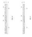
- FIG. 5 illustrates side cross-sectional views of microelectronic package, according to an embodiment of the present description.
- FIG. 6 illustrates side cross-sectional views of microelectronic package, according to another embodiment of the present description.
- FIG. 7 is a flow diagram of a process of fabricating a microelectronic structure, according to an embodiment of the present description.
- FIGS. 8A-8F illustrate a side cross-sectional view of a process of integrating the high density glass flex layer in a microelectronic package, according to another embodiment of the present description.
- FIG. 9 is a flow diagram of a process of fabricating a microelectronic structure, according to an embodiment of the present description.
- FIG. 10 illustrates an electronic system/device, according to one implementation of the present description.
- Embodiments of the present description relate to the field of fabricating microelectronic structures.
- the microelectronic structures may include a glass routing structure formed separately from a trace routing structure, wherein the glass routing structure is incorporated with the trace routing substrate, either in a laminated or embedded configuration.
- the glass routing structure can achieve high density trace routing, such that the density requirements may be relaxed on the trace routing substrate, which may result in reduced cost and allow for the fabrication of thin trace routing substrates.
- a microelectronic package including at least one microelectronic device disposed proximate to the glass routing structure of the microelectronic substrate and coupled with the microelectronic substrate by a plurality of interconnects.
- a microelectronic structure including at least one microelectronic device embedded within a microelectronic encapsulant having a glass routing structure attached to the microelectronic encapsulant and a trace routing structure formed on the glass routing structure.
- the disclosed embodiments encompass a microelectronic substrate including a glass routing structure.
- the term “glass” refers to an amorphous solid.
- glass materials that may be used with the described embodiments include substantially pure silica (e.g., approximately 100% SiO2), soda-lime glass, boro-silicate glass, and alumino-silicate glass.
- the disclosed embodiments are not limited to silica-based glass compositions, and glasses having alternative base materials (e.g., fluoride glasses, phosphate glasses, chalcogen glasses, ceramic materials (such as alumina), etc.) may also be employed with the disclosed embodiments.
- any combination of other materials and additives may be combined with silica (or other base material) to form a glass having desired physical properties.
- these additives include not only the aforementioned calcium carbonate (e.g., lime) and sodium carbonate (e.g., soda), but also magnesium, calcium, manganese, aluminum, lead, boron, iron, chromium, potassium, sulfur, and antimony, as well as carbonates and/or oxides of these and other elements.
- the aforementioned glasses and additives are but a few examples of the many types of materials and material combinations that may find application with the disclosed embodiments.
- a glass layer or structure may include surface treatments and/or coatings to improve strength and/or durability.
- a glass layer or structure may also be annealed to lower internal stresses.
- a glass routing structure may be formed in a manner shown in FIGS. 1A-1J .
- a thin glass layer 102 may be provided, wherein a plurality of through holes 108 are formed to extend through the glass layer 102 from a first surface 104 to a second surface 106 thereof.
- the glass layer 102 may be between about 15 ⁇ m and about 100 ⁇ m in thickness T.
- the glass layer through holes 108 may have a high density, which may be defined as having center-to-center pitches of less than about 45 ⁇ m.
- the glass layer through holes 108 may be formed by any known technique, including but not limited to imprinting, sand blasting, laser drilling, dry (e.g. plasma based) or wet etching, and the like.
- the glass layer second surface 106 may be attached to a first temporary carrier 112 with a first temporary adhesive layer 114 .
- the first temporary carrier 112 may be any appropriate, substantially rigid, support structure and the first temporary adhesive layer 114 may be any appropriate adhesive material, as will be understood to those skilled in the art.
- a filler layer 116 may be deposited over the glass layer first surface 104 , into the glass layer through holes 108 , and abutting portions of the first temporary adhesive layer 114 within the glass layer through holes 108 .
- the filler layer 116 may be any appropriate material, including but not limited to a titanium/aluminum alloy.
- the glass layer 102 may be removed, flipped, and attached by the filler layer 116 to a second temporary carrier 122 with a second temporary adhesive layer 124 .
- the second temporary carrier 122 may be any appropriate, substantially rigid, support structure, and may be the same as the first temporary carrier.
- the second temporary adhesive layer 124 may be any appropriate adhesive material, as will be understood to those skilled in the art, and may be the same material as the first temporary adhesive layer 114 .
- a plurality of conductive traces 132 may be formed on the glass layer second surface 106 .
- the glass surface conductive traces 132 may be any appropriate conductive material, including but not limited to copper, aluminum, and alloys thereof. Additionally, the glass surface conductive traces 132 may be formed by any appropriate technique, including, but not limited to deposition, plating, and lamination, followed by patterning, such as lithography. The process as described in FIG.
- 1A-1D may result in high density conductive traces having 2/2 ⁇ m or finer line/space.
- at least one of the plurality of glass surface conductive traces 132 may span between at least two glass layer through holes 108 .
- the glass surface conductive traces 132 may have any appropriate shape including expanded portions 134 proximate the glass layer through holes 108 (see FIG. 1D ), and may have an opening 136 through the expanded portion 134 , which will allow for the electrical connection of the glass surface conductive traces 132 to various microelectronic elements to be formed, as will be discussed.
- the glass layer 102 may be removed, flipped, and attached by the glass layer first surface 104 to a third temporary carrier 142 with a third temporary adhesive layer 144 .
- the third temporary carrier 142 may be any appropriate, substantially rigid, support structure, and may be the first temporary carrier 112 or the second temporary carrier 122 .
- the third temporary adhesive layer 144 may be any appropriate material having sufficient adhesive properties, as will be understood to those skilled in the art.
- the filler layer 116 may be removed by any technique known in the art, including but not limited to etching.
- the glass layer 102 may be removed from the third temporary carrier 142 and any residue of third temporary adhesive layer 144 removed, as shown in FIG. 1J , to form the glass routing structure 100 .
- the glass routing structure 100 could have a plurality of glass layers (shown as elements 102 1 , 102 2 , and 102 3 ), a plurality of glass surface conductive traces (shown as elements 132 1 and 132 2 ), and a plurality of conductive vias (shown as elements 146 ) extending through the glass layers (shown as elements 102 1 , 102 2 , and 102 3 ).
- the process for the fabrication of the glass routing structure 100 shown in FIG. 1K will be apparent to those skilled in the art based on the present description.
- a microelectronic substrate may be formed in a manner shown in FIGS. 2A-2F .
- the glass layer first surface 104 may be attached to a tape film 202 .
- a trace routing structure 204 may be provided.
- the trace routing structure 204 may in include a plurality of dielectric layers having conductive routes formed therein and therethrough.
- the trace route structure 204 may include at least one first level conductive trace 212 1 formed on a first level dielectric layer 214 1 , wherein at least one first level conductive via 216 1 may be formed to extend through the first level dielectric layer 214 1 and be connected to further conductive structures (not shown).
- a second level dielectric layer 214 2 may be formed on the first level dielectric layer 214 1 and the first level conductive traces 212 1 . At least one second level conductive trace 212 2 may be formed on the second level dielectric layer 214 2 , wherein at least one second level conductive trace 212 2 may electrically contact at least one first level conductive trace 212 1 through at least one second level conductive via 216 2 extending through the second level dielectric layer 214 2 . It is understood that the process of forming conductive traces and dielectric layers is repeated until a desired number is achieved to form the trace routing structure 204 . It is further understood that the final conductive trace (illustrated as element 212 2 ) may be a landing pad, as known in the art.
- the conductive traces may be composed of any conductive material, including but not limited to metals, such as copper and aluminum, and alloys thereof.
- metals such as copper and aluminum
- alloys thereof e.g. copper and aluminum
- a semi-additive, subtractive, or damascene process may be used, as will be understood to those skilled in the art.
- a subtractive process may be used, as will be understood to those skilled in the art. It is also understood that diffusion barriers to prevent ions of the conductive material from migrating may be required, particularly with the use of copper.
- the dielectric layers may be compose of any appropriate dielectric, including but not limited to silicon dioxide (SiO 2 ), silicon oxynitride (SiO x N y ), and silicon nitride (Si 3 N 4 ) and silicon carbide (SiC), as well as silica-filled epoxies and the like.
- the dielectric layers are formed of silicon dioxide by a plasma enhance chemical vapor deposition process.
- the dielectric layers are an organic dielectric that may be formed by printing or lamination.
- the conductive vias may be formed in the dielectric layers (e.g. elements 216 1 and 216 2 ) may be formed by forming an opening therethrough by dry or wet etching, laser ablation, ion drilling, a combination of these, or the like, and filling the opening with a conductive material, such in manner described with regard to the formation of the conductive traces (e.g. elements 212 1 and 212 2 ).
- a dielectric adhesive material layer 222 may be formed over the trace routing structure 204 .
- the dielectric adhesive material layer 222 may be an organic adhesive material and may be laminated or printed over the trace routing structure 204 .
- the dielectric adhesive material layer 222 may be partially cured to retain adhesive properties, while still being soft enough to conform to a shape a subsequently attached glass routing structure.
- the glass routing structure 100 of FIG. 1J may be aligned on the dielectric adhesive material layer 222 of FIG. 2C . Pressure may be applied for lamination as the dielectric adhesive material layer 222 is cured and the tape film 202 (see FIG. 2A ) may then be removed.
- the glass layer 102 may be used a hard mask to etch openings 232 through the dielectric adhesive material layer 222 to expose a portion of at least one first level conductive trace 212 1 .
- the openings 232 may be formed with an oxygen plasma etching process.
- the openings 232 of FIG. 2 e may be filled with a conductive material to form through-glass contacts, such as conductive bumps 234 thereby forming a microelectronic substrate 250 .
- a semi-additive plating process may be used to form the conductive bumps 234 .
- the conductive bumps 234 may be any appropriate conductive material, including but not limited to copper, aluminum, and alloys thereof.
- the dielectric adhesive material layer 222 may be applied to the glass layer second surface 106 , as shown in FIG. 3 .
- the dielectric adhesive material layer 222 may then be attached to the trace routing structure 204 to form the structure shown in FIG. 2D .
- the through-glass contacts may be formed of a solder material.
- underbump metallization layers 402 may be formed to substantially cover the surfaces within each of the glass layer through holes 108 and the openings 232 , as shown in FIG. 4A .
- the purposes and processes (such as deposition, plating, etching, planarization, and the like) for forming the underbump metallization layers 402 are well known in the art.
- a solder material may be deposited within each of the glass layer through holes 108 (see FIG. 4A ) and the openings 232 (see FIG.
- solder contacts 404 may be made of any appropriate material, including, but not limited to, lead/tin alloys and high tin content alloys (e.g. 90% or more tin), and similar alloys.
- FIGS. 1A-1K , 2 A- 2 F, 3 , 4 A, and 4 B may be a portion of a microelectronic package 500 illustrated in FIG. 5 .
- at least one microelectronic device 502 such as a microprocessor, a chipset, a graphics device, a wireless device, a memory device, an application specific integrated circuit, or the like, may be electrically attached through bond pads 504 thereon to mirror image through-glass contacts, such as conductive bumps 234 .
- the trace routing structure 204 may include the first level dielectric layer 214 1 and the second level dielectric layer 214 2 , as shown in FIGS.
- the trace routing structure 204 may further include a core structure 508 within the additional dielectric layers 514 1 - 514 4 , a solder resist layer 516 , and external interconnects 518 .
- the conductive traces and conductive vias (such as conductive traces 212 1 / 212 2 and conductive vias 216 1 / 216 2 of FIGS.
- the glass surface conductive traces 132 may provide high bandwidth communication between adjacent microelectronic devices 502 and/or may be used as high density escape routes.
- the microelectronic device 502 may include a plurality of conductive traces 522 forming electronic connections between the microelectronic device bond pads 504 and integrated circuitry 524 within the microelectronic device 502 , wherein the microelectronic device conductive traces 522 have an average pitch (e.g.
- the trace routing structure 204 comprising a plurality of dielectric layers and conductive traces, wherein the trace routing structure conductive traces (see elements 212 1 and 212 2 of FIGS. 2B-2F ) may also have an average pitch and the glass routing structure conductive traces 132 may have an average pitch.
- the average pitch of the glass routing structure conductive traces 132 is greater than the average pitch of the microelectronic device conductive traces 522 and less than the average pitch of the trace routing structure conductive traces (see elements 212 1 and 212 2 of FIGS. 2B-2F ).
- FIG. 6 illustrates a microelectronic package 600 which is similar to that of the microelectronic package 500 of FIG. 5 with the exception that microelectronic devices 502 are attached with the solder contacts 404 of FIGS. 4A-4B .
- a glass routing structure may be formed comprising a glass layer having at least one through hole extending from a first surface of the glass layer to a second surface of the glass layer, and at least one conductive trace formed on the glass layer second surface.
- a trace routing structure may be formed comprising a plurality of dielectric layers and conductive traces. The glass routing structure second surface may be adhered to the trace routing structure with the dielectric adhesive material layer, as defined in block 730 .
- At least one opening may be formed through the dielectric adhesive material layer to expose at least one trace routing structure conductive trace, as defined in block 740 .
- at least one conductive via may be formed within the at least one opening.
- a glass layer may be embedded in a microelectronic package.
- an encapsulated structure 802 may be provided having at least one microelectronic device 804 embedded within an encapsulation material 806 , such that an active surface 812 of the microelectronic device 804 may be substantially planar with a first surface 814 of the encapsulation material 806 , such that the microelectronic device active surface 812 does not have encapsulation material 806 thereon.
- the encapsulated structure 802 may be placed on a temporary carrier 822 .
- the glass routing structure 100 may be adhered to the at least one microelectronic device active surface 812 and the encapsulation material first surface 814 with the dielectric adhesive material layer 222 .
- the dielectric adhesive material layer 222 may be first applied to the glass routing structure 100 or may be first applied to the at least one microelectronic device active surface 812 and the encapsulation material first surface 814 .
- a first dielectric layer 824 may be disposed over the glass routing structure 100 and into the glass layer through holes 108 .
- at least one via 826 may be formed through the first dielectric layer 824 and the glass layer through holes 108 to expose at least one glass surface conductive trace 132 , or may be formed through the first dielectric layer 824 , through the glass layer through holes 108 , and through the dielectric adhesive material layer 222 to expose at least one bond pad 832 of the microelectronic device 802 .
- the vias 826 may be formed by any technique known in the art, including, but not limited to, laser drilling.
- At least one conductive via 834 may be formed by filling at least one via 826 with a conductive material.
- the vias 826 may be filled by any technique known in the art, including, but not limited to, additive plating.
- the conductive vias 834 may be composed of any conductive material, including but not limited to metals, such as copper and aluminum, and alloys thereof.
- a trace routing structure 842 may be formed on the first dielectric layer 824 and the conductive vias 834 in a manner as previously discussed with regard to the formation of the trace routing structure 204 of FIGS.
- At least one dielectric layer may be formed with conductive traces and vias formed thereon and therethrough (not shown for clarity and brevity) and may terminate in at least one external interconnect 846 , as will be understood to those skilled in the art.
- the temporary carrier 822 may be removed to form the microelectronic package 800 .
- the microelectronic device 804 may include a plurality of conductive traces 852 forming electronic connections between the microelectronic device bond pads 832 and integrated circuitry 854 within the microelectronic device 502 , wherein the microelectronic device conductive traces 852 have an average pitch (e.g. average width between conductive traces).
- the trace routing structure 842 comprising a plurality of dielectric layers and conductive traces, wherein the trace routing structure conductive traces (see elements 212 1 and 212 2 of FIGS. 2B-2F ) may also have an average pitch and the glass routing structure conductive traces 132 may have an average pitch.
- the average pitch of the glass routing structure conductive traces 132 is greater than the average pitch of the microelectronic device conductive traces 852 and less than the average pitch of the trace routing structure conductive traces (see elements 212 1 and 212 2 of FIGS. 2B-2F ).
- an encapsulated structure may be formed having at least one microelectronic device embedded within an encapsulation material such that an active surface of the microelectronic device may be substantially planar with a first surface of the encapsulation material.
- a glass routing structure may be formed comprising a glass layer having at least one through hole extending from a first surface of the glass layer to a second surface of the glass layer, and at least one conductive trace formed on the glass layer second surface, as defined in block 920 .
- the glass routing structure may be adhered to the at least one microelectronic device active surface and the encapsulation material first surface with the dielectric adhesive material layer.
- a first dielectric layer may be formed over the glass routing structure and into the glass layer through holes, as defined in block 940 .
- At least one via may be formed through the first dielectric layer and the glass layer through holes to expose at least one glass surface conductive trace, or may be formed through the first dielectric layer, through the glass layer through holes, and through the dielectric adhesive material layer to expose at least one bond pad of the at least one microelectronic device, as defined in block 950 .
- at least one conductive via may be formed by filling at least one via with a conductive material.
- a trace routing structure may be formed on the first dielectric layer and the conductive vias, which may be in electrical communication with at least one conductive via, as defined in block 970 .
- FIG. 10 illustrates an embodiment of a electronic system/device 1000 , such as a portable computer, a desktop computer, a mobile telephone, a digital camera, a digital music player, a web tablet/pad device, a personal digital assistant, a pager, an instant messaging device, or other devices.
- the electronic system/device 1000 may be adapted to transmit and/or receive information wirelessly, such as through a wireless local area network (WLAN) system, a wireless personal area network (WPAN) system, and/or a cellular network.
- the electronic system/device 1000 may include a microelectronic motherboard 1010 disposed within a device housing 1020 .
- a microelectronic package 1030 may be attached to the microelectronic motherboard 1010 .
- the microelectronic package 1030 may include a microelectronic substrate (not shown) comprising a trace routing structure (not shown) having a glass routing structure incorporated on (e.g. laminated) or in (e.g. embedded) the trace routing substrate.
- the microelectronic motherboard 1010 may be attached to various peripheral devices including an input device 1050 , such as keypad, and a display device 1060 , such an LCD display. It is understood that the display device 1060 may also function as the input device, if the display device 1060 is touch sensitive.
Landscapes
- Engineering & Computer Science (AREA)
- Microelectronics & Electronic Packaging (AREA)
- Power Engineering (AREA)
- Computer Hardware Design (AREA)
- Physics & Mathematics (AREA)
- General Physics & Mathematics (AREA)
- Condensed Matter Physics & Semiconductors (AREA)
- Manufacturing & Machinery (AREA)
- Ceramic Engineering (AREA)
- Chemical & Material Sciences (AREA)
- Geometry (AREA)
- Inorganic Chemistry (AREA)
- Production Of Multi-Layered Print Wiring Board (AREA)
Abstract
Description
Claims (7)
Priority Applications (3)
| Application Number | Priority Date | Filing Date | Title |
|---|---|---|---|
| US13/625,406 US9001520B2 (en) | 2012-09-24 | 2012-09-24 | Microelectronic structures having laminated or embedded glass routing structures for high density packaging |
| US14/618,235 US9642248B2 (en) | 2012-09-24 | 2015-02-10 | Microelectronic structures having laminated or embedded glass routing structures for high density packaging |
| US15/469,964 US10008452B2 (en) | 2012-09-24 | 2017-03-27 | Microelectronic structures having laminated or embedded glass routing structures for high density packaging |
Applications Claiming Priority (1)
| Application Number | Priority Date | Filing Date | Title |
|---|---|---|---|
| US13/625,406 US9001520B2 (en) | 2012-09-24 | 2012-09-24 | Microelectronic structures having laminated or embedded glass routing structures for high density packaging |
Related Child Applications (1)
| Application Number | Title | Priority Date | Filing Date |
|---|---|---|---|
| US14/618,235 Division US9642248B2 (en) | 2012-09-24 | 2015-02-10 | Microelectronic structures having laminated or embedded glass routing structures for high density packaging |
Publications (2)
| Publication Number | Publication Date |
|---|---|
| US20140085846A1 US20140085846A1 (en) | 2014-03-27 |
| US9001520B2 true US9001520B2 (en) | 2015-04-07 |
Family
ID=50338640
Family Applications (3)
| Application Number | Title | Priority Date | Filing Date |
|---|---|---|---|
| US13/625,406 Active 2033-01-30 US9001520B2 (en) | 2012-09-24 | 2012-09-24 | Microelectronic structures having laminated or embedded glass routing structures for high density packaging |
| US14/618,235 Active 2032-12-11 US9642248B2 (en) | 2012-09-24 | 2015-02-10 | Microelectronic structures having laminated or embedded glass routing structures for high density packaging |
| US15/469,964 Active US10008452B2 (en) | 2012-09-24 | 2017-03-27 | Microelectronic structures having laminated or embedded glass routing structures for high density packaging |
Family Applications After (2)
| Application Number | Title | Priority Date | Filing Date |
|---|---|---|---|
| US14/618,235 Active 2032-12-11 US9642248B2 (en) | 2012-09-24 | 2015-02-10 | Microelectronic structures having laminated or embedded glass routing structures for high density packaging |
| US15/469,964 Active US10008452B2 (en) | 2012-09-24 | 2017-03-27 | Microelectronic structures having laminated or embedded glass routing structures for high density packaging |
Country Status (1)
| Country | Link |
|---|---|
| US (3) | US9001520B2 (en) |
Cited By (3)
| Publication number | Priority date | Publication date | Assignee | Title |
|---|---|---|---|---|
| US9420707B2 (en) | 2009-12-17 | 2016-08-16 | Intel Corporation | Substrate for integrated circuit devices including multi-layer glass core and methods of making the same |
| CN106711097A (en) * | 2015-11-13 | 2017-05-24 | 台湾积体电路制造股份有限公司 | Structure and formation method for chip package |
| US9686861B2 (en) | 2009-12-17 | 2017-06-20 | Intel Corporation | Glass core substrate for integrated circuit devices and methods of making the same |
Families Citing this family (13)
| Publication number | Priority date | Publication date | Assignee | Title |
|---|---|---|---|---|
| US9445496B2 (en) | 2012-03-07 | 2016-09-13 | Intel Corporation | Glass clad microelectronic substrate |
| US9642261B2 (en) * | 2014-01-24 | 2017-05-02 | Zhuhai Advanced Chip Carriers & Electronic Substrate Solutions Technologies Co. Ltd. | Composite electronic structure with partially exposed and protruding copper termination posts |
| JP2015213138A (en) * | 2014-05-07 | 2015-11-26 | イビデン株式会社 | Package substrate and manufacturing method of the same |
| JP6409442B2 (en) * | 2014-09-22 | 2018-10-24 | イビデン株式会社 | Package substrate |
| JP6539992B2 (en) * | 2014-11-14 | 2019-07-10 | 凸版印刷株式会社 | Printed circuit board, semiconductor device, method of manufacturing wired circuit board, method of manufacturing semiconductor device |
| US20170287838A1 (en) | 2016-04-02 | 2017-10-05 | Intel Corporation | Electrical interconnect bridge |
| EP3606301A1 (en) * | 2017-04-10 | 2020-02-05 | Hitachi Chemical Company, Ltd. | Circuit board production method, circuit sheet and circuit board |
| US10651117B2 (en) | 2018-06-22 | 2020-05-12 | Intel Corporation | Low-inductance current paths for on-package power distributions and methods of assembling same |
| CN108770201A (en) * | 2018-08-07 | 2018-11-06 | 中国航空工业集团公司雷华电子技术研究所 | A kind of microwave circuit flush type pcb |
| JP7512594B2 (en) * | 2020-01-10 | 2024-07-09 | Toppanホールディングス株式会社 | Circuit Board |
| CN112802757B (en) * | 2020-12-28 | 2022-08-05 | 广东佛智芯微电子技术研究有限公司 | Substrate preparation method, substrate structure, chip packaging method and chip packaging structure |
| CN112802758B (en) * | 2020-12-28 | 2022-08-05 | 广东佛智芯微电子技术研究有限公司 | Substrate preparation method, substrate structure, chip packaging method and chip packaging structure |
| US20230317618A1 (en) * | 2022-03-29 | 2023-10-05 | Intel Corporation | Glass bridge for connecting dies |
Citations (110)
| Publication number | Priority date | Publication date | Assignee | Title |
|---|---|---|---|---|
| US4221047A (en) | 1979-03-23 | 1980-09-09 | International Business Machines Corporation | Multilayered glass-ceramic substrate for mounting of semiconductor device |
| US4327143A (en) | 1981-01-23 | 1982-04-27 | Westinghouse Electric Corp. | Moisture resistant laminates impregnated with an impregnating composition comprising epoxy resin and a dicyandiamide derivative |
| US4379553A (en) | 1979-07-20 | 1983-04-12 | General Electric Company | Bowling lane with fire retardant decorative surface |
| US4639543A (en) | 1985-02-04 | 1987-01-27 | Richard J. Birch | Semiconductor devices having a metallic glass substrate |
| US4664309A (en) | 1983-06-30 | 1987-05-12 | Raychem Corporation | Chip mounting device |
| US4828597A (en) | 1987-12-07 | 1989-05-09 | General Electric Company | Flexible glass fiber mat bonding method |
| US4975103A (en) | 1988-09-07 | 1990-12-04 | Schott Glaswerke | Process for producing a planar glass substrate coated with a dielectric layer system |
| US5193668A (en) | 1990-04-28 | 1993-03-16 | Sharp Kabushiki Kaisha | Touch-sensitive panel and display apparatus using the touch-sensitive panel |
| US5294238A (en) | 1991-03-27 | 1994-03-15 | Semiconductor Energy Laboratory Co., Ltd. | Glass substrate for a semiconductor device and method for making same |
| JPH06237081A (en) | 1993-02-10 | 1994-08-23 | Matsushita Electric Ind Co Ltd | Manufacture of multilayer ceramic substrate |
| US5466488A (en) | 1993-02-08 | 1995-11-14 | Mitsubishi Materials Corporation | Method of making glazed AlN substrate with an Al2 O3 -SiO2 interfacial layer |
| US5585675A (en) | 1994-05-11 | 1996-12-17 | Harris Corporation | Semiconductor die packaging tub having angularly offset pad-to-pad via structure configured to allow three-dimensional stacking and electrical interconnections among multiple identical tubs |
| US5612171A (en) | 1992-02-24 | 1997-03-18 | Corning Incorporated | Planar optical waveguides with planar optical elements |
| US5611876A (en) | 1993-06-28 | 1997-03-18 | Harris Corporation | Method of making a multilayer LTCC tub architecture for hermetically sealing semiconductor die, external electrical access for which is provided by way of sidewall recesses |
| US5668405A (en) * | 1994-09-14 | 1997-09-16 | Nec Corporation | Semiconductor device with a film carrier tape |
| US5705855A (en) | 1995-01-13 | 1998-01-06 | Motorola, Inc. | Integrated circuit for directly attaching to a glass substrate and method for manufacturing the same |
| US5917652A (en) | 1996-02-05 | 1999-06-29 | Minnesota Mining And Manufacturing Company | Durable retroreflective elements |
| US5981880A (en) | 1996-08-20 | 1999-11-09 | International Business Machines Corporation | Electronic device packages having glass free non conductive layers |
| US6023098A (en) * | 1995-06-29 | 2000-02-08 | Fujitsu Limited | Semiconductor device having terminals for heat radiation |
| US6037656A (en) * | 1996-08-12 | 2000-03-14 | Nec Corporation | Semiconductor integrated circuit device having short signal paths to terminals and process of fabrication thereof |
| JP2000119047A (en) | 1998-10-08 | 2000-04-25 | Nippon Sheet Glass Co Ltd | Glass laminate and its production |
| US6156413A (en) | 1996-10-25 | 2000-12-05 | Canon Kabushiki Kaisha | Glass circuit substrate and fabrication method thereof |
| US6177707B1 (en) | 1998-03-02 | 2001-01-23 | U.S. Philips Corporation | Semiconductor device comprising a glass supporting body onto which a substrate with semiconductor elements and a metalization is attached by means of an adhesive |
| JP2001053191A (en) | 1999-08-05 | 2001-02-23 | Fujitsu Ltd | Substrate derived from electrode protrusion and method of manufacturing the same |
| US6194762B1 (en) | 1996-02-09 | 2001-02-27 | Semiconductor Energy Laboratory Co., Ltd. | Complementary metal oxide semiconductor (CMOS) device comprising thin-film transistors arranged on a glass substrate |
| US6309901B1 (en) | 1997-10-24 | 2001-10-30 | Agfa-Gevaert | Use of glass laminate as a substrate in semiconductor devices |
| US6320547B1 (en) | 1998-08-07 | 2001-11-20 | Sarnoff Corporation | Switch structure for antennas formed on multilayer ceramic substrates |
| US20010042854A1 (en) | 2000-04-25 | 2001-11-22 | Murata Manufacturing Co., Ltd. | Electroconductive composition and printed circuit board using the same |
| US6329610B1 (en) | 1997-06-03 | 2001-12-11 | Kabushiki Kaisha Toshiba | Hybrid wiring board, semiconductor apparatus, flexible substrate, and fabrication method of hybrid wiring board |
| US6339197B1 (en) | 1999-05-27 | 2002-01-15 | Hoya Corporation | Multilayer printed circuit board and the manufacturing method |
| US20020038725A1 (en) | 2000-08-21 | 2002-04-04 | Matsushita Electric Industrial Co., Ltd. | Circuit board and production of the same |
| US20020145197A1 (en) | 2001-03-23 | 2002-10-10 | Ngk Spark Plug Co., Ltd. | Wiring substrate |
| US20020159243A1 (en) | 2000-12-12 | 2002-10-31 | Ngk Spark Plug Co., Ltd. | Wiring board |
| US20020182958A1 (en) | 2001-04-23 | 2002-12-05 | Fujitsu Limited | Multilayer printed wiring board |
| US20020180015A1 (en) | 2001-05-31 | 2002-12-05 | Yoshihide Yamaguchi | Semiconductor module |
| US6534723B1 (en) | 1999-11-26 | 2003-03-18 | Ibiden Co., Ltd. | Multilayer printed-circuit board and semiconductor device |
| US6539750B1 (en) | 1999-04-30 | 2003-04-01 | Matsushita Electric Industrial Co., Ltd. | Glass substrate forming mold and production method for glass substrate |
| US20030063453A1 (en) | 2001-09-28 | 2003-04-03 | Fujitsu Limited | Multilayer wiring circuit board |
| JP2003142804A (en) | 2001-10-31 | 2003-05-16 | Kyocera Corp | Circuit board |
| EP1164823A3 (en) | 2000-06-14 | 2003-09-10 | Matsushita Electric Industrial Co., Ltd. | Printed circuit board and method of manufacturing the same |
| US6673698B1 (en) | 2002-01-19 | 2004-01-06 | Megic Corporation | Thin film semiconductor package utilizing a glass substrate with composite polymer/metal interconnect layers |
| US20040071960A1 (en) | 2000-04-18 | 2004-04-15 | Andreas Weber | Glass body with improved strength |
| US20040137701A1 (en) * | 2002-10-11 | 2004-07-15 | Sanyo Electric Co., Ltd. | Semiconductor device and manufacturing method thereof |
| US20040151882A1 (en) | 2002-09-26 | 2004-08-05 | Fujitsu Limited | Wiring board with core layer containing inorganic filler |
| US6772514B2 (en) | 2000-06-12 | 2004-08-10 | Matsushita Electric Industrial Co., Ltd. | Method of machining glass substrate and method fabricating high-frequency circuit |
| US20040168825A1 (en) | 2000-02-25 | 2004-09-02 | Hajime Sakamoto | Multilayer printed circuit board and multilayer printed circuit board manufacturing method |
| US20040178492A1 (en) | 2001-09-28 | 2004-09-16 | Toppan Printing Co., Ltd. | Multi-layer wiring board, IC package, and method of manufacturing multi-layer wiring board |
| US6799438B2 (en) | 2000-07-15 | 2004-10-05 | Schott Glas | Method for making a microstructure in a glass or plastic substrate according to hot-forming technology and associated forming tool |
| US20040217455A1 (en) | 2001-07-12 | 2004-11-04 | Osamu Shiono | Wiring glass substrate and method of manufacturing the wiring glass substrate, conductive paste and semiconductor module used for wiring glass substrate, and method of forming wiring substrate and conductor |
| US20040239349A1 (en) | 2002-07-23 | 2004-12-02 | Fujitsu Limited | Probe card and testing method of semiconductor chip, capacitor and manufacturing method thereof |
| JP2005005488A (en) | 2003-06-12 | 2005-01-06 | Dainippon Printing Co Ltd | Semiconductor module and its manufacturing method |
| US6839946B2 (en) | 1996-10-17 | 2005-01-11 | Nokia Corporation | Method for fabricating a thin film bulk acoustic wave resonator (FBAR) on a glass substrate |
| US20050012217A1 (en) | 2002-12-11 | 2005-01-20 | Toshiaki Mori | Multilayer wiring board and manufacture method thereof |
| US20050016764A1 (en) | 2003-07-25 | 2005-01-27 | Fumio Echigo | Wiring substrate for intermediate connection and multi-layered wiring board and their production |
| US6894358B2 (en) | 2001-08-24 | 2005-05-17 | Schott Glas | Process for producing microelectromechanical components and a housed microelectromechanical component |
| US20050189136A1 (en) | 1999-10-26 | 2005-09-01 | Ibiden Co., Ltd. | Multi-layer printed circuit board and method of manufacturing multi-layer printed circuit board |
| US20050218503A1 (en) | 2003-01-16 | 2005-10-06 | Fujitsu Limited | Multilayer wiring board, method for producing the same, and method for producing fiber reinforced resin board |
| US20060005382A1 (en) | 2004-07-12 | 2006-01-12 | Unitech Printed Circuit Board Corporation | Modular method for manufacturing circuit board |
| US6989604B1 (en) | 2002-06-06 | 2006-01-24 | Advanced Micro Devices, Inc. | Conformal barrier liner in an integrated circuit interconnect |
| US20060043572A1 (en) | 2004-08-27 | 2006-03-02 | Ngk Spark Plug Co., Ltd. | Wiring board |
| US7038309B2 (en) | 2002-09-09 | 2006-05-02 | Via Technologies, Inc. | Chip package structure with glass substrate |
| US7072018B2 (en) | 2001-06-08 | 2006-07-04 | Sanyo Electric Co., Ltd. | IC substrate of glass and display device |
| US20060201818A1 (en) | 2003-09-09 | 2006-09-14 | Hoya Corporation | Manufacturing method of double-sided wiring glass substrate |
| JP2006275954A (en) | 2005-03-30 | 2006-10-12 | Railway Technical Res Inst | Bearing monitoring system and bearing monitoring program |
| US20060244128A1 (en) | 2005-04-19 | 2006-11-02 | Renesas Technology Corp. | Semiconductor device and method of manufacturing the same |
| US20060261364A1 (en) * | 2003-03-10 | 2006-11-23 | Yoshinobu Suehiro | Solid element device and method for manufacturing thereof |
| US20060289968A1 (en) | 2005-06-28 | 2006-12-28 | Micron Technology, Inc. | Conductive interconnect structures and formation methods using supercritical fluids |
| US7164572B1 (en) | 2005-09-15 | 2007-01-16 | Medtronic, Inc. | Multi-path, mono-polar co-fired hermetic electrical feedthroughs and methods of fabrication therfor |
| US7176131B2 (en) | 2002-04-09 | 2007-02-13 | Infineon Technologies Ag | Electronic component having at least one semiconductor chip and flip-chip contacts, and method for producing the same |
| US20070060970A1 (en) | 2005-09-15 | 2007-03-15 | Burdon Jeremy W | Miniaturized co-fired electrical interconnects for implantable medical devices |
| KR100701205B1 (en) | 2005-01-12 | 2007-03-29 | 박성호 | Laminating material joining method and device |
| US20070096328A1 (en) | 2005-07-07 | 2007-05-03 | Ibiden Co., Ltd. | Multilayered printed wiring board |
| US20070119619A1 (en) * | 2005-08-29 | 2007-05-31 | Shinko Electric Industries Co., Ltd. | Multilayered wiring board and method for fabricating the same |
| US20070154741A1 (en) | 2005-07-07 | 2007-07-05 | Ibiden Co., Ltd. | Multilayer printed wiring board |
| US7259080B2 (en) | 2002-09-06 | 2007-08-21 | Fraunhofer-Gesellschaft Zur Forderung Der Angewandten Forschung E.V. | Glass-type planar substrate, use thereof, and method for the production thereof |
| US20070230151A1 (en) | 2006-03-31 | 2007-10-04 | Fujitsu Limited | Circuit substrate and electronic apparatus, fabrication process thereof |
| US7279771B2 (en) | 2004-03-31 | 2007-10-09 | Shinko Electric Industries Co., Ltd. | Wiring board mounting a capacitor |
| US20070257356A1 (en) * | 2004-08-25 | 2007-11-08 | Fujitsu Limited | Semiconductor device having multilayer printed wiring board and manufacturing method of the same |
| US20070267138A1 (en) | 2003-03-28 | 2007-11-22 | White George E | Methods for Fabricating Three-Dimensional All Organic Interconnect Structures |
| US7307852B2 (en) | 1999-09-02 | 2007-12-11 | Ibiden Co., Ltd. | Printed circuit board and method for manufacturing printed circuit board |
| US7337540B2 (en) | 2003-11-18 | 2008-03-04 | Seiko Epson Corporation | Method of manufacturing a structure body bonding with a glass substrate and semiconductor substrate |
| US20080073110A1 (en) | 2006-09-26 | 2008-03-27 | Fujitsu Limited | Interposer and method for manufacturing the same |
| US7362403B2 (en) | 2004-01-30 | 2008-04-22 | Funai Electric Co., Ltd. | Liquid crystal display having gate driver IC chip COG-mounted on glass substrate |
| US20080107863A1 (en) | 2006-11-03 | 2008-05-08 | Ibiden Co., Ltd | Multilayered printed wiring board |
| US20080152928A1 (en) | 2006-12-26 | 2008-06-26 | Tdk Corporation | Multilayer ceramics substrate |
| US20080149384A1 (en) | 2006-12-21 | 2008-06-26 | Ngk Spark Plug Co., Ltd. | Multilayer wiring board and power supply structure to be embedded in multilayer wiring board |
| US20080164057A1 (en) | 2003-07-30 | 2008-07-10 | Hiroyuki Mori | Printed Wiring Board And Method Of Manufacturing Same |
| US20080217748A1 (en) | 2007-03-08 | 2008-09-11 | International Business Machines Corporation | Low cost and low coefficient of thermal expansion packaging structures and processes |
| US20080261005A1 (en) | 2006-02-14 | 2008-10-23 | Murata Manufacturing Co., Ltd. | Multilayer ceramic electronic component, multilayer ceramic substrate, and method for manufacturing multilayer ceramic electronic component |
| US20080277148A1 (en) | 1999-06-02 | 2008-11-13 | Ibiden Co., Ltd | Multi-layer printed circuit board and method of manufacturing multilayer printed circuit board |
| US20080283277A1 (en) | 2007-05-14 | 2008-11-20 | Shinko Electric Industries Co., Ltd. | Wiring board manufacturing method and wiring board |
| US20090001550A1 (en) | 2007-06-28 | 2009-01-01 | Yonggang Li | Method of Forming a Multilayer Substrate Core Structure Using Sequential Microvia Laser Drilling And Substrate Core Structure Formed According to the Method |
| US7476623B2 (en) | 2004-10-09 | 2009-01-13 | Schott Ag | Method for microstructuring flat glass substrates |
| US20090159316A1 (en) | 2007-12-19 | 2009-06-25 | Shinko Electric Industries Co., Ltd. | Wiring substrate and method of manufacturing the same |
| US20090183910A1 (en) | 2008-01-22 | 2009-07-23 | Shinko Electric Industries Co., Ltd. | Wiring board and method of manufacturing the same |
| US20090243065A1 (en) | 2006-04-27 | 2009-10-01 | Mitsuo Sugino | Semiconductor Device and Method for Manufacturing Semiconductor Device |
| US20090273073A1 (en) | 2007-03-30 | 2009-11-05 | Kenya Tachibana | Connecting structure for flip-chip semiconductor package, build-up layer material, sealing resin composition, and circuit board |
| US20090294161A1 (en) | 2008-05-30 | 2009-12-03 | Fujitsu Limited | Core substrate and printed wiring board |
| US20090293271A1 (en) | 2008-06-02 | 2009-12-03 | Ibiden Co., Ltd. | Printed wiring board with built-in electronic component and manufacturing method thereof |
| JP2009302506A (en) | 2008-05-14 | 2009-12-24 | Toppan Printing Co Ltd | Multilayer substrate for semiconductor package and manufacturing method thereof |
| US20100019382A1 (en) | 2008-07-23 | 2010-01-28 | Renesas Technology Corp. | Semiconductor device and method for manufacturing the same |
| US20100032826A1 (en) | 2006-12-05 | 2010-02-11 | Sumitomo Bakelite Company Limited | Semiconductor package, core layer material, buildup layer material, and sealing resin composition |
| US20100164030A1 (en) | 2008-12-31 | 2010-07-01 | International Business Machines Corporation | Chip carrier bearing large silicon for high performance computing and related method |
| US7749900B2 (en) | 2008-09-30 | 2010-07-06 | Intel Corporation | Method and core materials for semiconductor packaging |
| US20110147055A1 (en) | 2009-12-17 | 2011-06-23 | Qing Ma | Glass core substrate for integrated circuit devices and methods of making the same |
| US20110147059A1 (en) | 2009-12-17 | 2011-06-23 | Qing Ma | Substrate for integrated circuit devices including multi-layer glass core and methods of making the same |
| US7993510B2 (en) | 1999-08-06 | 2011-08-09 | Ibiden Co., Ltd. | Electroplating solution, method for manufacturing multilayer printed circuit board using the same solution, and multilayer printed circuit board |
| US20110233786A1 (en) * | 2010-03-24 | 2011-09-29 | Soichi Homma | Semiconductor device and method for manufacturing the same |
| US20120106117A1 (en) * | 2010-11-02 | 2012-05-03 | Georgia Tech Research Corporation | Ultra-thin interposer assemblies with through vias |
| WO2013133827A1 (en) | 2012-03-07 | 2013-09-12 | Intel Corporation | Glass clad microelectronic substrate |
Family Cites Families (8)
| Publication number | Priority date | Publication date | Assignee | Title |
|---|---|---|---|---|
| US3958317A (en) | 1974-09-25 | 1976-05-25 | Rockwell International Corporation | Copper surface treatment for epoxy bonding |
| JPS61116881A (en) | 1984-11-12 | 1986-06-04 | Nippon Soken Inc | How to connect electrodes |
| JPH05267853A (en) | 1992-03-23 | 1993-10-15 | Nec Toyama Ltd | Manufacture of multilayer printed circuit board |
| JP4221859B2 (en) | 1999-02-12 | 2009-02-12 | 株式会社デンソー | Manufacturing method of semiconductor device |
| KR100919674B1 (en) | 2002-12-27 | 2009-10-06 | 주식회사 하이닉스반도체 | Manufacturing Method of Semiconductor Device |
| KR100594327B1 (en) | 2005-03-24 | 2006-06-30 | 삼성전자주식회사 | A semiconductor device having nanowires having a round cross section and a method of manufacturing the same |
| US20070090416A1 (en) | 2005-09-28 | 2007-04-26 | Doyle Brian S | CMOS devices with a single work function gate electrode and method of fabrication |
| TW200933899A (en) | 2008-01-29 | 2009-08-01 | Sanyo Electric Co | Mesa type semiconductor device and method for making the same |
-
2012
- 2012-09-24 US US13/625,406 patent/US9001520B2/en active Active
-
2015
- 2015-02-10 US US14/618,235 patent/US9642248B2/en active Active
-
2017
- 2017-03-27 US US15/469,964 patent/US10008452B2/en active Active
Patent Citations (139)
| Publication number | Priority date | Publication date | Assignee | Title |
|---|---|---|---|---|
| US4221047A (en) | 1979-03-23 | 1980-09-09 | International Business Machines Corporation | Multilayered glass-ceramic substrate for mounting of semiconductor device |
| US4379553A (en) | 1979-07-20 | 1983-04-12 | General Electric Company | Bowling lane with fire retardant decorative surface |
| US4327143A (en) | 1981-01-23 | 1982-04-27 | Westinghouse Electric Corp. | Moisture resistant laminates impregnated with an impregnating composition comprising epoxy resin and a dicyandiamide derivative |
| US4664309A (en) | 1983-06-30 | 1987-05-12 | Raychem Corporation | Chip mounting device |
| US4639543A (en) | 1985-02-04 | 1987-01-27 | Richard J. Birch | Semiconductor devices having a metallic glass substrate |
| US4828597A (en) | 1987-12-07 | 1989-05-09 | General Electric Company | Flexible glass fiber mat bonding method |
| US4975103A (en) | 1988-09-07 | 1990-12-04 | Schott Glaswerke | Process for producing a planar glass substrate coated with a dielectric layer system |
| US5193668A (en) | 1990-04-28 | 1993-03-16 | Sharp Kabushiki Kaisha | Touch-sensitive panel and display apparatus using the touch-sensitive panel |
| US5294238A (en) | 1991-03-27 | 1994-03-15 | Semiconductor Energy Laboratory Co., Ltd. | Glass substrate for a semiconductor device and method for making same |
| US5612171A (en) | 1992-02-24 | 1997-03-18 | Corning Incorporated | Planar optical waveguides with planar optical elements |
| US5466488A (en) | 1993-02-08 | 1995-11-14 | Mitsubishi Materials Corporation | Method of making glazed AlN substrate with an Al2 O3 -SiO2 interfacial layer |
| JPH06237081A (en) | 1993-02-10 | 1994-08-23 | Matsushita Electric Ind Co Ltd | Manufacture of multilayer ceramic substrate |
| US5611876A (en) | 1993-06-28 | 1997-03-18 | Harris Corporation | Method of making a multilayer LTCC tub architecture for hermetically sealing semiconductor die, external electrical access for which is provided by way of sidewall recesses |
| US5585675A (en) | 1994-05-11 | 1996-12-17 | Harris Corporation | Semiconductor die packaging tub having angularly offset pad-to-pad via structure configured to allow three-dimensional stacking and electrical interconnections among multiple identical tubs |
| US5668405A (en) * | 1994-09-14 | 1997-09-16 | Nec Corporation | Semiconductor device with a film carrier tape |
| US5705855A (en) | 1995-01-13 | 1998-01-06 | Motorola, Inc. | Integrated circuit for directly attaching to a glass substrate and method for manufacturing the same |
| US6023098A (en) * | 1995-06-29 | 2000-02-08 | Fujitsu Limited | Semiconductor device having terminals for heat radiation |
| US5917652A (en) | 1996-02-05 | 1999-06-29 | Minnesota Mining And Manufacturing Company | Durable retroreflective elements |
| US6194762B1 (en) | 1996-02-09 | 2001-02-27 | Semiconductor Energy Laboratory Co., Ltd. | Complementary metal oxide semiconductor (CMOS) device comprising thin-film transistors arranged on a glass substrate |
| US6037656A (en) * | 1996-08-12 | 2000-03-14 | Nec Corporation | Semiconductor integrated circuit device having short signal paths to terminals and process of fabrication thereof |
| US5981880A (en) | 1996-08-20 | 1999-11-09 | International Business Machines Corporation | Electronic device packages having glass free non conductive layers |
| US6781064B1 (en) | 1996-08-20 | 2004-08-24 | International Business Machines Corporation | Printed circuit boards for electronic device packages having glass free non-conductive layers and method of forming same |
| US6839946B2 (en) | 1996-10-17 | 2005-01-11 | Nokia Corporation | Method for fabricating a thin film bulk acoustic wave resonator (FBAR) on a glass substrate |
| US6156413A (en) | 1996-10-25 | 2000-12-05 | Canon Kabushiki Kaisha | Glass circuit substrate and fabrication method thereof |
| US20020046880A1 (en) | 1997-06-03 | 2002-04-25 | Kabushiki Kaisha Toshiba | Hybrid wiring board, semiconductor apparatus, flexible substrate, and fabrication method of hybrid wiring board |
| US6329610B1 (en) | 1997-06-03 | 2001-12-11 | Kabushiki Kaisha Toshiba | Hybrid wiring board, semiconductor apparatus, flexible substrate, and fabrication method of hybrid wiring board |
| US6309901B1 (en) | 1997-10-24 | 2001-10-30 | Agfa-Gevaert | Use of glass laminate as a substrate in semiconductor devices |
| US6177707B1 (en) | 1998-03-02 | 2001-01-23 | U.S. Philips Corporation | Semiconductor device comprising a glass supporting body onto which a substrate with semiconductor elements and a metalization is attached by means of an adhesive |
| US6320547B1 (en) | 1998-08-07 | 2001-11-20 | Sarnoff Corporation | Switch structure for antennas formed on multilayer ceramic substrates |
| JP2000119047A (en) | 1998-10-08 | 2000-04-25 | Nippon Sheet Glass Co Ltd | Glass laminate and its production |
| US6539750B1 (en) | 1999-04-30 | 2003-04-01 | Matsushita Electric Industrial Co., Ltd. | Glass substrate forming mold and production method for glass substrate |
| US6339197B1 (en) | 1999-05-27 | 2002-01-15 | Hoya Corporation | Multilayer printed circuit board and the manufacturing method |
| US20060191710A1 (en) | 1999-05-27 | 2006-08-31 | Hoya Corporation | Multilayer printed wiring board and a process of producing same |
| US20080277148A1 (en) | 1999-06-02 | 2008-11-13 | Ibiden Co., Ltd | Multi-layer printed circuit board and method of manufacturing multilayer printed circuit board |
| JP2001053191A (en) | 1999-08-05 | 2001-02-23 | Fujitsu Ltd | Substrate derived from electrode protrusion and method of manufacturing the same |
| US7993510B2 (en) | 1999-08-06 | 2011-08-09 | Ibiden Co., Ltd. | Electroplating solution, method for manufacturing multilayer printed circuit board using the same solution, and multilayer printed circuit board |
| US7307852B2 (en) | 1999-09-02 | 2007-12-11 | Ibiden Co., Ltd. | Printed circuit board and method for manufacturing printed circuit board |
| US20080283282A1 (en) | 1999-10-26 | 2008-11-20 | Ibiden Co., Ltd. | Multi-layer printed circuit board and method of manufacturing multi-layer printed circuit board |
| US20060191708A1 (en) | 1999-10-26 | 2006-08-31 | Ibiden Co., Ltd. | Multi-layer printed circuit board and method of manufacturing multi-layer printed circuit board |
| US20050189136A1 (en) | 1999-10-26 | 2005-09-01 | Ibiden Co., Ltd. | Multi-layer printed circuit board and method of manufacturing multi-layer printed circuit board |
| US20100006328A1 (en) | 1999-10-26 | 2010-01-14 | Ibiden Co., Ltd. | Multi-layer printed circuit board and method of manufacturing multi-layer printed circuit board |
| US6534723B1 (en) | 1999-11-26 | 2003-03-18 | Ibiden Co., Ltd. | Multilayer printed-circuit board and semiconductor device |
| US20070227765A1 (en) | 2000-02-25 | 2007-10-04 | Ibiden Co., Ltd. | Multilayer printed circuit board and multilayer printed circuit board manufacturing method |
| US20040168825A1 (en) | 2000-02-25 | 2004-09-02 | Hajime Sakamoto | Multilayer printed circuit board and multilayer printed circuit board manufacturing method |
| US20040071960A1 (en) | 2000-04-18 | 2004-04-15 | Andreas Weber | Glass body with improved strength |
| US20010042854A1 (en) | 2000-04-25 | 2001-11-22 | Murata Manufacturing Co., Ltd. | Electroconductive composition and printed circuit board using the same |
| US6772514B2 (en) | 2000-06-12 | 2004-08-10 | Matsushita Electric Industrial Co., Ltd. | Method of machining glass substrate and method fabricating high-frequency circuit |
| EP1164823A3 (en) | 2000-06-14 | 2003-09-10 | Matsushita Electric Industrial Co., Ltd. | Printed circuit board and method of manufacturing the same |
| US6799438B2 (en) | 2000-07-15 | 2004-10-05 | Schott Glas | Method for making a microstructure in a glass or plastic substrate according to hot-forming technology and associated forming tool |
| US20030066683A1 (en) | 2000-08-21 | 2003-04-10 | Matsushita Electric Industrial Co., Ltd. | Circuit board and production of the same |
| US20020038725A1 (en) | 2000-08-21 | 2002-04-04 | Matsushita Electric Industrial Co., Ltd. | Circuit board and production of the same |
| US6691409B2 (en) | 2000-08-21 | 2004-02-17 | Matsushita Electric Industrial Co., Ltd. | Method of producing a circuit board |
| US20020159243A1 (en) | 2000-12-12 | 2002-10-31 | Ngk Spark Plug Co., Ltd. | Wiring board |
| US20020145197A1 (en) | 2001-03-23 | 2002-10-10 | Ngk Spark Plug Co., Ltd. | Wiring substrate |
| US20020182958A1 (en) | 2001-04-23 | 2002-12-05 | Fujitsu Limited | Multilayer printed wiring board |
| US20020180015A1 (en) | 2001-05-31 | 2002-12-05 | Yoshihide Yamaguchi | Semiconductor module |
| US7072018B2 (en) | 2001-06-08 | 2006-07-04 | Sanyo Electric Co., Ltd. | IC substrate of glass and display device |
| US20040217455A1 (en) | 2001-07-12 | 2004-11-04 | Osamu Shiono | Wiring glass substrate and method of manufacturing the wiring glass substrate, conductive paste and semiconductor module used for wiring glass substrate, and method of forming wiring substrate and conductor |
| US7071521B2 (en) | 2001-08-24 | 2006-07-04 | Schott Ag | Process for producing microelectromechanical components and a housed microelectromechanical component |
| US7285834B2 (en) | 2001-08-24 | 2007-10-23 | Schott Ag | Process for producing microelectromechanical components and a housed microelectromechanical component |
| US6894358B2 (en) | 2001-08-24 | 2005-05-17 | Schott Glas | Process for producing microelectromechanical components and a housed microelectromechanical component |
| US20030063453A1 (en) | 2001-09-28 | 2003-04-03 | Fujitsu Limited | Multilayer wiring circuit board |
| EP1298972A3 (en) | 2001-09-28 | 2005-08-17 | Fujitsu Limited | Multilayer wiring circuit board |
| US20050098882A1 (en) | 2001-09-28 | 2005-05-12 | Fujitsu Limited | Multilayer wiring circuit board |
| US20040178492A1 (en) | 2001-09-28 | 2004-09-16 | Toppan Printing Co., Ltd. | Multi-layer wiring board, IC package, and method of manufacturing multi-layer wiring board |
| US20070175025A1 (en) | 2001-09-28 | 2007-08-02 | Toppan Printing Co., Ltd. | Method of manufacturing multi-layer wiring board |
| JP2003142804A (en) | 2001-10-31 | 2003-05-16 | Kyocera Corp | Circuit board |
| US6673698B1 (en) | 2002-01-19 | 2004-01-06 | Megic Corporation | Thin film semiconductor package utilizing a glass substrate with composite polymer/metal interconnect layers |
| US7176131B2 (en) | 2002-04-09 | 2007-02-13 | Infineon Technologies Ag | Electronic component having at least one semiconductor chip and flip-chip contacts, and method for producing the same |
| US6989604B1 (en) | 2002-06-06 | 2006-01-24 | Advanced Micro Devices, Inc. | Conformal barrier liner in an integrated circuit interconnect |
| US20060255817A1 (en) | 2002-07-23 | 2006-11-16 | Fujitsu Limited | Probe card and testing method of semiconductor chip, capacitor and manufacturing method thereof |
| US20060255816A1 (en) | 2002-07-23 | 2006-11-16 | Fujitsu Limited | Probe card and testing method of semiconductor chip, capacitor and manufacturing method thereof |
| US20040239349A1 (en) | 2002-07-23 | 2004-12-02 | Fujitsu Limited | Probe card and testing method of semiconductor chip, capacitor and manufacturing method thereof |
| US7259080B2 (en) | 2002-09-06 | 2007-08-21 | Fraunhofer-Gesellschaft Zur Forderung Der Angewandten Forschung E.V. | Glass-type planar substrate, use thereof, and method for the production thereof |
| US7038309B2 (en) | 2002-09-09 | 2006-05-02 | Via Technologies, Inc. | Chip package structure with glass substrate |
| US20040151882A1 (en) | 2002-09-26 | 2004-08-05 | Fujitsu Limited | Wiring board with core layer containing inorganic filler |
| US20040137701A1 (en) * | 2002-10-11 | 2004-07-15 | Sanyo Electric Co., Ltd. | Semiconductor device and manufacturing method thereof |
| US20050012217A1 (en) | 2002-12-11 | 2005-01-20 | Toshiaki Mori | Multilayer wiring board and manufacture method thereof |
| US7091589B2 (en) | 2002-12-11 | 2006-08-15 | Dai Nippon Printing Co., Ltd. | Multilayer wiring board and manufacture method thereof |
| US20050218503A1 (en) | 2003-01-16 | 2005-10-06 | Fujitsu Limited | Multilayer wiring board, method for producing the same, and method for producing fiber reinforced resin board |
| US20070186414A1 (en) | 2003-01-16 | 2007-08-16 | Fujitsu Limited | Multilayer wiring board incorporating carbon fibers and glass fibers |
| US20060261364A1 (en) * | 2003-03-10 | 2006-11-23 | Yoshinobu Suehiro | Solid element device and method for manufacturing thereof |
| US20110101399A1 (en) * | 2003-03-10 | 2011-05-05 | Toyoda Gosei Co., Ltd. | Solid element device and method for manufacturing the same |
| US20070267138A1 (en) | 2003-03-28 | 2007-11-22 | White George E | Methods for Fabricating Three-Dimensional All Organic Interconnect Structures |
| JP2005005488A (en) | 2003-06-12 | 2005-01-06 | Dainippon Printing Co Ltd | Semiconductor module and its manufacturing method |
| US20050016764A1 (en) | 2003-07-25 | 2005-01-27 | Fumio Echigo | Wiring substrate for intermediate connection and multi-layered wiring board and their production |
| US20080164057A1 (en) | 2003-07-30 | 2008-07-10 | Hiroyuki Mori | Printed Wiring Board And Method Of Manufacturing Same |
| US20060201201A1 (en) | 2003-09-09 | 2006-09-14 | Hoya Corporation | Manufacturing method of double-sided wiring glass substrate |
| US20060201818A1 (en) | 2003-09-09 | 2006-09-14 | Hoya Corporation | Manufacturing method of double-sided wiring glass substrate |
| US7337540B2 (en) | 2003-11-18 | 2008-03-04 | Seiko Epson Corporation | Method of manufacturing a structure body bonding with a glass substrate and semiconductor substrate |
| US7362403B2 (en) | 2004-01-30 | 2008-04-22 | Funai Electric Co., Ltd. | Liquid crystal display having gate driver IC chip COG-mounted on glass substrate |
| US7279771B2 (en) | 2004-03-31 | 2007-10-09 | Shinko Electric Industries Co., Ltd. | Wiring board mounting a capacitor |
| US20060005382A1 (en) | 2004-07-12 | 2006-01-12 | Unitech Printed Circuit Board Corporation | Modular method for manufacturing circuit board |
| US20070257356A1 (en) * | 2004-08-25 | 2007-11-08 | Fujitsu Limited | Semiconductor device having multilayer printed wiring board and manufacturing method of the same |
| US20060043572A1 (en) | 2004-08-27 | 2006-03-02 | Ngk Spark Plug Co., Ltd. | Wiring board |
| US7476623B2 (en) | 2004-10-09 | 2009-01-13 | Schott Ag | Method for microstructuring flat glass substrates |
| KR100701205B1 (en) | 2005-01-12 | 2007-03-29 | 박성호 | Laminating material joining method and device |
| JP2006275954A (en) | 2005-03-30 | 2006-10-12 | Railway Technical Res Inst | Bearing monitoring system and bearing monitoring program |
| US20060244128A1 (en) | 2005-04-19 | 2006-11-02 | Renesas Technology Corp. | Semiconductor device and method of manufacturing the same |
| US20090174065A1 (en) | 2005-04-19 | 2009-07-09 | Renesas Technology Corp. | Semiconductor device and method of manufacturing the same |
| US20060289968A1 (en) | 2005-06-28 | 2006-12-28 | Micron Technology, Inc. | Conductive interconnect structures and formation methods using supercritical fluids |
| US20070096328A1 (en) | 2005-07-07 | 2007-05-03 | Ibiden Co., Ltd. | Multilayered printed wiring board |
| US20070154741A1 (en) | 2005-07-07 | 2007-07-05 | Ibiden Co., Ltd. | Multilayer printed wiring board |
| US20070119619A1 (en) * | 2005-08-29 | 2007-05-31 | Shinko Electric Industries Co., Ltd. | Multilayered wiring board and method for fabricating the same |
| US20070060970A1 (en) | 2005-09-15 | 2007-03-15 | Burdon Jeremy W | Miniaturized co-fired electrical interconnects for implantable medical devices |
| US7164572B1 (en) | 2005-09-15 | 2007-01-16 | Medtronic, Inc. | Multi-path, mono-polar co-fired hermetic electrical feedthroughs and methods of fabrication therfor |
| US20080261005A1 (en) | 2006-02-14 | 2008-10-23 | Murata Manufacturing Co., Ltd. | Multilayer ceramic electronic component, multilayer ceramic substrate, and method for manufacturing multilayer ceramic electronic component |
| US20070230151A1 (en) | 2006-03-31 | 2007-10-04 | Fujitsu Limited | Circuit substrate and electronic apparatus, fabrication process thereof |
| US20090243065A1 (en) | 2006-04-27 | 2009-10-01 | Mitsuo Sugino | Semiconductor Device and Method for Manufacturing Semiconductor Device |
| US20080073110A1 (en) | 2006-09-26 | 2008-03-27 | Fujitsu Limited | Interposer and method for manufacturing the same |
| US20080107863A1 (en) | 2006-11-03 | 2008-05-08 | Ibiden Co., Ltd | Multilayered printed wiring board |
| US20100032826A1 (en) | 2006-12-05 | 2010-02-11 | Sumitomo Bakelite Company Limited | Semiconductor package, core layer material, buildup layer material, and sealing resin composition |
| US20080149384A1 (en) | 2006-12-21 | 2008-06-26 | Ngk Spark Plug Co., Ltd. | Multilayer wiring board and power supply structure to be embedded in multilayer wiring board |
| US20080152928A1 (en) | 2006-12-26 | 2008-06-26 | Tdk Corporation | Multilayer ceramics substrate |
| US20080217748A1 (en) | 2007-03-08 | 2008-09-11 | International Business Machines Corporation | Low cost and low coefficient of thermal expansion packaging structures and processes |
| US20090273073A1 (en) | 2007-03-30 | 2009-11-05 | Kenya Tachibana | Connecting structure for flip-chip semiconductor package, build-up layer material, sealing resin composition, and circuit board |
| US20080283277A1 (en) | 2007-05-14 | 2008-11-20 | Shinko Electric Industries Co., Ltd. | Wiring board manufacturing method and wiring board |
| US20090001550A1 (en) | 2007-06-28 | 2009-01-01 | Yonggang Li | Method of Forming a Multilayer Substrate Core Structure Using Sequential Microvia Laser Drilling And Substrate Core Structure Formed According to the Method |
| US20090159316A1 (en) | 2007-12-19 | 2009-06-25 | Shinko Electric Industries Co., Ltd. | Wiring substrate and method of manufacturing the same |
| US20090183910A1 (en) | 2008-01-22 | 2009-07-23 | Shinko Electric Industries Co., Ltd. | Wiring board and method of manufacturing the same |
| JP2009176791A (en) | 2008-01-22 | 2009-08-06 | Shinko Electric Ind Co Ltd | Wiring substrate and its manufacturing method |
| JP2009302506A (en) | 2008-05-14 | 2009-12-24 | Toppan Printing Co Ltd | Multilayer substrate for semiconductor package and manufacturing method thereof |
| US20090294161A1 (en) | 2008-05-30 | 2009-12-03 | Fujitsu Limited | Core substrate and printed wiring board |
| US20090293271A1 (en) | 2008-06-02 | 2009-12-03 | Ibiden Co., Ltd. | Printed wiring board with built-in electronic component and manufacturing method thereof |
| US20100019382A1 (en) | 2008-07-23 | 2010-01-28 | Renesas Technology Corp. | Semiconductor device and method for manufacturing the same |
| US7749900B2 (en) | 2008-09-30 | 2010-07-06 | Intel Corporation | Method and core materials for semiconductor packaging |
| US20100164030A1 (en) | 2008-12-31 | 2010-07-01 | International Business Machines Corporation | Chip carrier bearing large silicon for high performance computing and related method |
| WO2011084235A3 (en) | 2009-12-17 | 2011-09-09 | Intel Corporation | Glass core substrate for integrated circuit devices and methods of making the same |
| WO2011084216A2 (en) | 2009-12-17 | 2011-07-14 | Intel Corporation | Substrate for integrated circuit devices including multi-layer glass core and methods of making the same |
| WO2011084235A2 (en) | 2009-12-17 | 2011-07-14 | Intel Corporation | Glass core substrate for integrated circuit devices and methods of making the same |
| US20110147059A1 (en) | 2009-12-17 | 2011-06-23 | Qing Ma | Substrate for integrated circuit devices including multi-layer glass core and methods of making the same |
| WO2011084216A3 (en) | 2009-12-17 | 2011-09-09 | Intel Corporation | Substrate for integrated circuit devices including multi-layer glass core and methods of making the same |
| US20110147055A1 (en) | 2009-12-17 | 2011-06-23 | Qing Ma | Glass core substrate for integrated circuit devices and methods of making the same |
| US8207453B2 (en) | 2009-12-17 | 2012-06-26 | Intel Corporation | Glass core substrate for integrated circuit devices and methods of making the same |
| US20120192413A1 (en) | 2009-12-17 | 2012-08-02 | Qing Ma | Glass core substrate for integrated circuit devices and methods of making the same |
| US20110233786A1 (en) * | 2010-03-24 | 2011-09-29 | Soichi Homma | Semiconductor device and method for manufacturing the same |
| US20120106117A1 (en) * | 2010-11-02 | 2012-05-03 | Georgia Tech Research Corporation | Ultra-thin interposer assemblies with through vias |
| WO2013133827A1 (en) | 2012-03-07 | 2013-09-12 | Intel Corporation | Glass clad microelectronic substrate |
| US20140003009A1 (en) | 2012-03-07 | 2014-01-02 | Qing Ma | Glass clad microelectronic substrate |
Non-Patent Citations (27)
| Title |
|---|
| "Mems Tightly Sealed With Schott Hermes", Schott Electronic Packaging, Jul. 30, 2009. |
| "Schott Hermes", NEC Schott Components Corporation Japan, Copyright 2009, 2009. |
| International Preliminary Report on Patentability and Written Opinion received for PCT Patent Application No. PCT/US2012/028126, mailed on Sep. 18, 2014, 8 pages. |
| International Preliminary Report on Patentability Received for PCT Patent Application No. PCT/US2010/05493, Mailed on Jun. 28, 2012, 7. |
| International Preliminary Report on Patentability Received for PCT Patent Application No. PCT/US2010/054931, Mailed on Jun. 28, 2012, 7 pages. |
| International Preliminary Report on Patentability Received for PCT Patent Application No. PCT/US2010/056310, Mailed on Jun. 28, 2012, 7 pages. |
| International Search Report and Written Opinion Received for PCT Patent Application No. PCT/US2010/054931, Mailed on Jun. 30, 2011, 9 pages. |
| International Search Report and Written Opinion Received for PCT Patent Application No. PCT/US2010/056310, Mailed on Jun. 30, 2011, 9 pages. |
| International Search Report and written Opinion Received for PCT Patent Application No. PCT/US2012/28126, Mailed on Nov. 30, 2012, 11 pages. |
| Notice of Allowance received for Korean Patent Application No. 10-2012-7015462, mailed on Aug. 24, 2014, 1 page of English Translation and 2 pages of Notice of Allowance. |
| Notice of Allowance received for Korean Patent Application No. 2012-7015587, mailed on Apr. 9, 2014, 1 page of English Translation and 2 pages of JP NOA. |
| Office Action received for Chinese Patent Application No. 201080057189.8, mailed on May 4, 2014, 9 pages of English Translation and 7 pages of CN Office Action. |
| Office Action received for Chinese Patent Application No. 201080058105.2, mailed on Jun. 3, 2014, 4 pages of English Translation and 13 pages of CN Office Action. |
| Office Action received for German Patent Application No. 112010004888.6, mailed on Jul. 16, 2013, 5 pages of DE Office Action only. |
| Office Action received for German Patent Application No. 112010004890.8, mailed on Jul. 23. 2013, 7 pages ef DE Office Action only. |
| Office Action received for Japanese Patent Application No. 2012-542016, mailed on Jun. 25, 2013, 4 page of English Translation and 3 pages of JP Office Action. |
| Office Action received for Korean Patent Application No. 2012-7015462, mailed on Aug. 19, 2013, 3 pages of Office Action only. |
| Office Action received for Korean Patent Application No. 2012-7015462, mailed on Feb. 26, 2014, 2 pages of Office Action only. |
| Office Action received for Korean Patent Application No. 2012-7015587, mailed on Feb. 3, 2014, 3 pages English Translation only. |
| Office Action Received for Korean Patent Application No. 2012-7015587, mailed on Jun. 25, 2013, 4 pages of Office Action only. |
| Office Action received for Korean Patent Application No. 2014-7005894, mailed on Jun. 3, 2014, 2 pages of English Translation only. |
| Office Action received for Taiwan Patent Application No. 099136723, mailed on May 26, 2014, 16 pages of English Translation and 12 pages of TW Office Action. |
| Office Action received for Taiwan Patent Application No. 099137777, mailed on Dec. 19, 2013, 4 pages of English Translation and 5 pages of TW Office Action. |
| Office Action received for United Kingdom Patent Application No. 1208343.2, mailed on Aug. 22, 2013, 3 pages. |
| Office Action received for United Kingdom Patent Application No. 1208343.2, mailed on Dec. 19, 2013, 4 pages. |
| Onezawa, et al., "NEC Schott introduces Glass Substrates with Hermetic Metal Through Vias for WLP of MEMS & Sensor applications", Aug. 7, 2009. |
| Schott Hermes Substrate, Retrieved on Dec. 9, 2009, available at: http://www.nec-schott.co.jp/enplish/auto/others/hermes.html?PHPSESSID=r4nmcg11d95hgugh5r253hq3d3. |
Cited By (3)
| Publication number | Priority date | Publication date | Assignee | Title |
|---|---|---|---|---|
| US9420707B2 (en) | 2009-12-17 | 2016-08-16 | Intel Corporation | Substrate for integrated circuit devices including multi-layer glass core and methods of making the same |
| US9686861B2 (en) | 2009-12-17 | 2017-06-20 | Intel Corporation | Glass core substrate for integrated circuit devices and methods of making the same |
| CN106711097A (en) * | 2015-11-13 | 2017-05-24 | 台湾积体电路制造股份有限公司 | Structure and formation method for chip package |
Also Published As
| Publication number | Publication date |
|---|---|
| US20170200677A1 (en) | 2017-07-13 |
| US20150156869A1 (en) | 2015-06-04 |
| US9642248B2 (en) | 2017-05-02 |
| US20140085846A1 (en) | 2014-03-27 |
| US10008452B2 (en) | 2018-06-26 |
Similar Documents
| Publication | Publication Date | Title |
|---|---|---|
| US10008452B2 (en) | Microelectronic structures having laminated or embedded glass routing structures for high density packaging | |
| US9793201B2 (en) | Glass clad microelectronic substrate | |
| KR102596788B1 (en) | Package substrate with high-density interconnection layers with pillar and via connections for fan-out scaling | |
| US8198726B2 (en) | Through-hole electrode substrate and method of manufacturing the same | |
| EP2741341B1 (en) | Semiconductor device and fabrication method thereof | |
| ES2817788T3 (en) | Structure and procedure for a TSV with strain relief | |
| CN106057769B (en) | Microelectronic substrate for alternate encapsulation function | |
| WO2010067610A1 (en) | Semiconductor module, method for manufacturing semiconductor module, and portable apparatus | |
| JP2015043438A (en) | Substrate for integrated circuit devices including multi-layer glass core and methods of making the same | |
| US20210159153A1 (en) | Through electrode substrate and semiconductor device | |
| US20140048959A1 (en) | Microelectronic package having non-coplanar, encapsulated microelectronic devices and a bumpless build-up layer | |
| TWI690045B (en) | Assembly structure, method of bonding using the same, and circuit board therefor | |
| TWI230991B (en) | Semiconductor device and fabrication process thereof | |
| WO2018125454A1 (en) | Integrated circuit interconnect structure having metal oxide adhesive layer | |
| JP2008300718A (en) | Semiconductor device, and manufacturing method of semiconductor device | |
| JP5091962B2 (en) | Semiconductor device | |
| TW201032389A (en) | Wireless transceiver module | |
| JP2017005081A (en) | Interposer, semiconductor device, and method of manufacturing them | |
| WO2003095712A3 (en) | Method of and apparatus for forming three-dimensional structures integral with semiconductor based circuitry | |
| US7910478B2 (en) | Method of manufacturing semiconductor devices | |
| TWI423410B (en) | Metal conductive structure and manufacturing method | |
| JP4863861B2 (en) | Semiconductor device | |
| JP2010232292A (en) | Semiconductor device manufacturing method and semiconductor device | |
| JP2005340578A (en) | Circuit device | |
| JP2005005484A (en) | Plating post type wiring board and its manufacturing method |
Legal Events
| Date | Code | Title | Description |
|---|---|---|---|
| AS | Assignment |
Owner name: INTEL CORPORATION, CALIFORNIA Free format text: ASSIGNMENT OF ASSIGNORS INTEREST;ASSIGNORS:MA, QING;SWAN, JOHANNA M;STARKSTON, ROBERT B;AND OTHERS;SIGNING DATES FROM 20120913 TO 20130111;REEL/FRAME:030501/0745 |
|
| FEPP | Fee payment procedure |
Free format text: PAYOR NUMBER ASSIGNED (ORIGINAL EVENT CODE: ASPN); ENTITY STATUS OF PATENT OWNER: LARGE ENTITY |
|
| AS | Assignment |
Owner name: INTEL CORPORATION, CALIFORNIA Free format text: CORRECTIVE ASSIGNMENT TO CORRECT THE PLEASE CORRECT THE EXECUTION DATE OF INVENTORS JOHN S. GUZEK TO 12.02.2014, AND ROBERT L. SANKMAN TO 01.21.2015 PREVIOUSLY RECORDED ON REEL 030501 FRAME 0745. ASSIGNOR(S) HEREBY CONFIRMS THE APPLICANT'S REPRESENTATIVE SUBMITS AN ASSIGNMENT CORRECTING THE ERROR IDENTIFIED ABOVE.;ASSIGNORS:MA, QING;SWAN, JOHANNA M.;STARKSON, ROBERT;AND OTHERS;SIGNING DATES FROM 20141201 TO 20150121;REEL/FRAME:034891/0936 |
|
| STCF | Information on status: patent grant |
Free format text: PATENTED CASE |
|
| MAFP | Maintenance fee payment |
Free format text: PAYMENT OF MAINTENANCE FEE, 4TH YEAR, LARGE ENTITY (ORIGINAL EVENT CODE: M1551); ENTITY STATUS OF PATENT OWNER: LARGE ENTITY Year of fee payment: 4 |
|
| MAFP | Maintenance fee payment |
Free format text: PAYMENT OF MAINTENANCE FEE, 8TH YEAR, LARGE ENTITY (ORIGINAL EVENT CODE: M1552); ENTITY STATUS OF PATENT OWNER: LARGE ENTITY Year of fee payment: 8 |