JP2012099517A - Semiconductor device and method of manufacturing the same - Google Patents
Semiconductor device and method of manufacturing the same Download PDFInfo
- Publication number
- JP2012099517A JP2012099517A JP2010243251A JP2010243251A JP2012099517A JP 2012099517 A JP2012099517 A JP 2012099517A JP 2010243251 A JP2010243251 A JP 2010243251A JP 2010243251 A JP2010243251 A JP 2010243251A JP 2012099517 A JP2012099517 A JP 2012099517A
- Authority
- JP
- Japan
- Prior art keywords
- gate electrode
- metal layer
- spacer
- semiconductor device
- forming
- Prior art date
- Legal status (The legal status is an assumption and is not a legal conclusion. Google has not performed a legal analysis and makes no representation as to the accuracy of the status listed.)
- Pending
Links
Images


Classifications
-
- H—ELECTRICITY
- H10—SEMICONDUCTOR DEVICES; ELECTRIC SOLID-STATE DEVICES NOT OTHERWISE PROVIDED FOR
- H10D—INORGANIC ELECTRIC SEMICONDUCTOR DEVICES
- H10D84/00—Integrated devices formed in or on semiconductor substrates that comprise only semiconducting layers, e.g. on Si wafers or on GaAs-on-Si wafers
- H10D84/80—Integrated devices formed in or on semiconductor substrates that comprise only semiconducting layers, e.g. on Si wafers or on GaAs-on-Si wafers characterised by the integration of at least one component covered by groups H10D12/00 or H10D30/00, e.g. integration of IGFETs
- H10D84/82—Integrated devices formed in or on semiconductor substrates that comprise only semiconducting layers, e.g. on Si wafers or on GaAs-on-Si wafers characterised by the integration of at least one component covered by groups H10D12/00 or H10D30/00, e.g. integration of IGFETs of only field-effect components
- H10D84/83—Integrated devices formed in or on semiconductor substrates that comprise only semiconducting layers, e.g. on Si wafers or on GaAs-on-Si wafers characterised by the integration of at least one component covered by groups H10D12/00 or H10D30/00, e.g. integration of IGFETs of only field-effect components of only insulated-gate FETs [IGFET]
- H10D84/85—Complementary IGFETs, e.g. CMOS
- H10D84/853—Complementary IGFETs, e.g. CMOS comprising FinFETs
-
- H—ELECTRICITY
- H10—SEMICONDUCTOR DEVICES; ELECTRIC SOLID-STATE DEVICES NOT OTHERWISE PROVIDED FOR
- H10D—INORGANIC ELECTRIC SEMICONDUCTOR DEVICES
- H10D62/00—Semiconductor bodies, or regions thereof, of devices having potential barriers
- H10D62/10—Shapes, relative sizes or dispositions of the regions of the semiconductor bodies; Shapes of the semiconductor bodies
- H10D62/113—Isolations within a component, i.e. internal isolations
- H10D62/115—Dielectric isolations, e.g. air gaps
-
- H—ELECTRICITY
- H10—SEMICONDUCTOR DEVICES; ELECTRIC SOLID-STATE DEVICES NOT OTHERWISE PROVIDED FOR
- H10D—INORGANIC ELECTRIC SEMICONDUCTOR DEVICES
- H10D62/00—Semiconductor bodies, or regions thereof, of devices having potential barriers
- H10D62/10—Shapes, relative sizes or dispositions of the regions of the semiconductor bodies; Shapes of the semiconductor bodies
- H10D62/13—Semiconductor regions connected to electrodes carrying current to be rectified, amplified or switched, e.g. source or drain regions
- H10D62/149—Source or drain regions of field-effect devices
- H10D62/151—Source or drain regions of field-effect devices of IGFETs
-
- H10D64/01316—
-
- H10D64/01318—
-
- H10D64/0132—
-
- H—ELECTRICITY
- H10—SEMICONDUCTOR DEVICES; ELECTRIC SOLID-STATE DEVICES NOT OTHERWISE PROVIDED FOR
- H10D—INORGANIC ELECTRIC SEMICONDUCTOR DEVICES
- H10D64/00—Electrodes of devices having potential barriers
- H10D64/01—Manufacture or treatment
- H10D64/017—Manufacture or treatment using dummy gates in processes wherein at least parts of the final gates are self-aligned to the dummy gates, i.e. replacement gate processes
-
- H—ELECTRICITY
- H10—SEMICONDUCTOR DEVICES; ELECTRIC SOLID-STATE DEVICES NOT OTHERWISE PROVIDED FOR
- H10D—INORGANIC ELECTRIC SEMICONDUCTOR DEVICES
- H10D64/00—Electrodes of devices having potential barriers
- H10D64/01—Manufacture or treatment
- H10D64/018—Spacers formed inside holes at the prospective gate locations, e.g. holes left by removing dummy gates
-
- H—ELECTRICITY
- H10—SEMICONDUCTOR DEVICES; ELECTRIC SOLID-STATE DEVICES NOT OTHERWISE PROVIDED FOR
- H10D—INORGANIC ELECTRIC SEMICONDUCTOR DEVICES
- H10D64/00—Electrodes of devices having potential barriers
- H10D64/01—Manufacture or treatment
- H10D64/021—Manufacture or treatment using multiple gate spacer layers, e.g. bilayered sidewall spacers
-
- H—ELECTRICITY
- H10—SEMICONDUCTOR DEVICES; ELECTRIC SOLID-STATE DEVICES NOT OTHERWISE PROVIDED FOR
- H10D—INORGANIC ELECTRIC SEMICONDUCTOR DEVICES
- H10D64/00—Electrodes of devices having potential barriers
- H10D64/20—Electrodes characterised by their shapes, relative sizes or dispositions
- H10D64/23—Electrodes carrying the current to be rectified, amplified, oscillated or switched, e.g. sources, drains, anodes or cathodes
- H10D64/251—Source or drain electrodes for field-effect devices
- H10D64/258—Source or drain electrodes for field-effect devices characterised by the relative positions of the source or drain electrodes with respect to the gate electrode
- H10D64/259—Source or drain electrodes being self-aligned with the gate electrode and having bottom surfaces higher than the interface between the channel and the gate dielectric
-
- H—ELECTRICITY
- H10—SEMICONDUCTOR DEVICES; ELECTRIC SOLID-STATE DEVICES NOT OTHERWISE PROVIDED FOR
- H10D—INORGANIC ELECTRIC SEMICONDUCTOR DEVICES
- H10D64/00—Electrodes of devices having potential barriers
- H10D64/20—Electrodes characterised by their shapes, relative sizes or dispositions
- H10D64/27—Electrodes not carrying the current to be rectified, amplified, oscillated or switched, e.g. gates
- H10D64/311—Gate electrodes for field-effect devices
- H10D64/411—Gate electrodes for field-effect devices for FETs
- H10D64/511—Gate electrodes for field-effect devices for FETs for IGFETs
- H10D64/512—Disposition of the gate electrodes, e.g. buried gates
-
- H—ELECTRICITY
- H10—SEMICONDUCTOR DEVICES; ELECTRIC SOLID-STATE DEVICES NOT OTHERWISE PROVIDED FOR
- H10D—INORGANIC ELECTRIC SEMICONDUCTOR DEVICES
- H10D64/00—Electrodes of devices having potential barriers
- H10D64/20—Electrodes characterised by their shapes, relative sizes or dispositions
- H10D64/27—Electrodes not carrying the current to be rectified, amplified, oscillated or switched, e.g. gates
- H10D64/311—Gate electrodes for field-effect devices
- H10D64/411—Gate electrodes for field-effect devices for FETs
- H10D64/511—Gate electrodes for field-effect devices for FETs for IGFETs
- H10D64/517—Gate electrodes for field-effect devices for FETs for IGFETs characterised by the conducting layers
- H10D64/518—Gate electrodes for field-effect devices for FETs for IGFETs characterised by the conducting layers characterised by their lengths or sectional shapes
-
- H—ELECTRICITY
- H10—SEMICONDUCTOR DEVICES; ELECTRIC SOLID-STATE DEVICES NOT OTHERWISE PROVIDED FOR
- H10D—INORGANIC ELECTRIC SEMICONDUCTOR DEVICES
- H10D64/00—Electrodes of devices having potential barriers
- H10D64/60—Electrodes characterised by their materials
- H10D64/66—Electrodes having a conductor capacitively coupled to a semiconductor by an insulator, e.g. MIS electrodes
- H10D64/665—Electrodes having a conductor capacitively coupled to a semiconductor by an insulator, e.g. MIS electrodes the conductor comprising a layer of elemental metal contacting the insulator, e.g. tungsten or molybdenum
- H10D64/666—Electrodes having a conductor capacitively coupled to a semiconductor by an insulator, e.g. MIS electrodes the conductor comprising a layer of elemental metal contacting the insulator, e.g. tungsten or molybdenum the conductor further comprising additional layers
-
- H—ELECTRICITY
- H10—SEMICONDUCTOR DEVICES; ELECTRIC SOLID-STATE DEVICES NOT OTHERWISE PROVIDED FOR
- H10D—INORGANIC ELECTRIC SEMICONDUCTOR DEVICES
- H10D64/00—Electrodes of devices having potential barriers
- H10D64/60—Electrodes characterised by their materials
- H10D64/66—Electrodes having a conductor capacitively coupled to a semiconductor by an insulator, e.g. MIS electrodes
- H10D64/667—Electrodes having a conductor capacitively coupled to a semiconductor by an insulator, e.g. MIS electrodes the conductor comprising a layer of alloy material, compound material or organic material contacting the insulator, e.g. TiN workfunction layers
- H10D64/668—Electrodes having a conductor capacitively coupled to a semiconductor by an insulator, e.g. MIS electrodes the conductor comprising a layer of alloy material, compound material or organic material contacting the insulator, e.g. TiN workfunction layers the layer being a silicide, e.g. TiSi2
-
- H—ELECTRICITY
- H10—SEMICONDUCTOR DEVICES; ELECTRIC SOLID-STATE DEVICES NOT OTHERWISE PROVIDED FOR
- H10D—INORGANIC ELECTRIC SEMICONDUCTOR DEVICES
- H10D64/00—Electrodes of devices having potential barriers
- H10D64/60—Electrodes characterised by their materials
- H10D64/66—Electrodes having a conductor capacitively coupled to a semiconductor by an insulator, e.g. MIS electrodes
- H10D64/671—Electrodes having a conductor capacitively coupled to a semiconductor by an insulator, e.g. MIS electrodes the conductor having lateral variation in doping or structure
-
- H—ELECTRICITY
- H10—SEMICONDUCTOR DEVICES; ELECTRIC SOLID-STATE DEVICES NOT OTHERWISE PROVIDED FOR
- H10D—INORGANIC ELECTRIC SEMICONDUCTOR DEVICES
- H10D64/00—Electrodes of devices having potential barriers
- H10D64/60—Electrodes characterised by their materials
- H10D64/66—Electrodes having a conductor capacitively coupled to a semiconductor by an insulator, e.g. MIS electrodes
- H10D64/68—Electrodes having a conductor capacitively coupled to a semiconductor by an insulator, e.g. MIS electrodes characterised by the insulator, e.g. by the gate insulator
- H10D64/691—Electrodes having a conductor capacitively coupled to a semiconductor by an insulator, e.g. MIS electrodes characterised by the insulator, e.g. by the gate insulator comprising metallic compounds, e.g. metal oxides or metal silicates
-
- H—ELECTRICITY
- H10—SEMICONDUCTOR DEVICES; ELECTRIC SOLID-STATE DEVICES NOT OTHERWISE PROVIDED FOR
- H10D—INORGANIC ELECTRIC SEMICONDUCTOR DEVICES
- H10D84/00—Integrated devices formed in or on semiconductor substrates that comprise only semiconducting layers, e.g. on Si wafers or on GaAs-on-Si wafers
- H10D84/01—Manufacture or treatment
- H10D84/0123—Integrating together multiple components covered by H10D12/00 or H10D30/00, e.g. integrating multiple IGBTs
- H10D84/0126—Integrating together multiple components covered by H10D12/00 or H10D30/00, e.g. integrating multiple IGBTs the components including insulated gates, e.g. IGFETs
- H10D84/0165—Integrating together multiple components covered by H10D12/00 or H10D30/00, e.g. integrating multiple IGBTs the components including insulated gates, e.g. IGFETs the components including complementary IGFETs, e.g. CMOS devices
- H10D84/017—Manufacturing their source or drain regions, e.g. silicided source or drain regions
-
- H—ELECTRICITY
- H10—SEMICONDUCTOR DEVICES; ELECTRIC SOLID-STATE DEVICES NOT OTHERWISE PROVIDED FOR
- H10D—INORGANIC ELECTRIC SEMICONDUCTOR DEVICES
- H10D84/00—Integrated devices formed in or on semiconductor substrates that comprise only semiconducting layers, e.g. on Si wafers or on GaAs-on-Si wafers
- H10D84/01—Manufacture or treatment
- H10D84/0123—Integrating together multiple components covered by H10D12/00 or H10D30/00, e.g. integrating multiple IGBTs
- H10D84/0126—Integrating together multiple components covered by H10D12/00 or H10D30/00, e.g. integrating multiple IGBTs the components including insulated gates, e.g. IGFETs
- H10D84/0165—Integrating together multiple components covered by H10D12/00 or H10D30/00, e.g. integrating multiple IGBTs the components including insulated gates, e.g. IGFETs the components including complementary IGFETs, e.g. CMOS devices
- H10D84/0172—Manufacturing their gate conductors
- H10D84/0177—Manufacturing their gate conductors the gate conductors having different materials or different implants
-
- H—ELECTRICITY
- H10—SEMICONDUCTOR DEVICES; ELECTRIC SOLID-STATE DEVICES NOT OTHERWISE PROVIDED FOR
- H10D—INORGANIC ELECTRIC SEMICONDUCTOR DEVICES
- H10D84/00—Integrated devices formed in or on semiconductor substrates that comprise only semiconducting layers, e.g. on Si wafers or on GaAs-on-Si wafers
- H10D84/01—Manufacture or treatment
- H10D84/0123—Integrating together multiple components covered by H10D12/00 or H10D30/00, e.g. integrating multiple IGBTs
- H10D84/0126—Integrating together multiple components covered by H10D12/00 or H10D30/00, e.g. integrating multiple IGBTs the components including insulated gates, e.g. IGFETs
- H10D84/0165—Integrating together multiple components covered by H10D12/00 or H10D30/00, e.g. integrating multiple IGBTs the components including insulated gates, e.g. IGFETs the components including complementary IGFETs, e.g. CMOS devices
- H10D84/0172—Manufacturing their gate conductors
- H10D84/0179—Manufacturing their gate conductors the gate conductors having different shapes or dimensions
-
- H—ELECTRICITY
- H10—SEMICONDUCTOR DEVICES; ELECTRIC SOLID-STATE DEVICES NOT OTHERWISE PROVIDED FOR
- H10D—INORGANIC ELECTRIC SEMICONDUCTOR DEVICES
- H10D84/00—Integrated devices formed in or on semiconductor substrates that comprise only semiconducting layers, e.g. on Si wafers or on GaAs-on-Si wafers
- H10D84/01—Manufacture or treatment
- H10D84/0123—Integrating together multiple components covered by H10D12/00 or H10D30/00, e.g. integrating multiple IGBTs
- H10D84/0126—Integrating together multiple components covered by H10D12/00 or H10D30/00, e.g. integrating multiple IGBTs the components including insulated gates, e.g. IGFETs
- H10D84/0165—Integrating together multiple components covered by H10D12/00 or H10D30/00, e.g. integrating multiple IGBTs the components including insulated gates, e.g. IGFETs the components including complementary IGFETs, e.g. CMOS devices
- H10D84/0184—Manufacturing their gate sidewall spacers
-
- H—ELECTRICITY
- H10—SEMICONDUCTOR DEVICES; ELECTRIC SOLID-STATE DEVICES NOT OTHERWISE PROVIDED FOR
- H10D—INORGANIC ELECTRIC SEMICONDUCTOR DEVICES
- H10D84/00—Integrated devices formed in or on semiconductor substrates that comprise only semiconducting layers, e.g. on Si wafers or on GaAs-on-Si wafers
- H10D84/01—Manufacture or treatment
- H10D84/0123—Integrating together multiple components covered by H10D12/00 or H10D30/00, e.g. integrating multiple IGBTs
- H10D84/0126—Integrating together multiple components covered by H10D12/00 or H10D30/00, e.g. integrating multiple IGBTs the components including insulated gates, e.g. IGFETs
- H10D84/0165—Integrating together multiple components covered by H10D12/00 or H10D30/00, e.g. integrating multiple IGBTs the components including insulated gates, e.g. IGFETs the components including complementary IGFETs, e.g. CMOS devices
- H10D84/0193—Integrating together multiple components covered by H10D12/00 or H10D30/00, e.g. integrating multiple IGBTs the components including insulated gates, e.g. IGFETs the components including complementary IGFETs, e.g. CMOS devices the components including FinFETs
-
- H—ELECTRICITY
- H10—SEMICONDUCTOR DEVICES; ELECTRIC SOLID-STATE DEVICES NOT OTHERWISE PROVIDED FOR
- H10D—INORGANIC ELECTRIC SEMICONDUCTOR DEVICES
- H10D84/00—Integrated devices formed in or on semiconductor substrates that comprise only semiconducting layers, e.g. on Si wafers or on GaAs-on-Si wafers
- H10D84/01—Manufacture or treatment
- H10D84/02—Manufacture or treatment characterised by using material-based technologies
- H10D84/03—Manufacture or treatment characterised by using material-based technologies using Group IV technology, e.g. silicon technology or silicon-carbide [SiC] technology
- H10D84/038—Manufacture or treatment characterised by using material-based technologies using Group IV technology, e.g. silicon technology or silicon-carbide [SiC] technology using silicon technology, e.g. SiGe
-
- H—ELECTRICITY
- H10—SEMICONDUCTOR DEVICES; ELECTRIC SOLID-STATE DEVICES NOT OTHERWISE PROVIDED FOR
- H10D—INORGANIC ELECTRIC SEMICONDUCTOR DEVICES
- H10D84/00—Integrated devices formed in or on semiconductor substrates that comprise only semiconducting layers, e.g. on Si wafers or on GaAs-on-Si wafers
- H10D84/80—Integrated devices formed in or on semiconductor substrates that comprise only semiconducting layers, e.g. on Si wafers or on GaAs-on-Si wafers characterised by the integration of at least one component covered by groups H10D12/00 or H10D30/00, e.g. integration of IGFETs
- H10D84/82—Integrated devices formed in or on semiconductor substrates that comprise only semiconducting layers, e.g. on Si wafers or on GaAs-on-Si wafers characterised by the integration of at least one component covered by groups H10D12/00 or H10D30/00, e.g. integration of IGFETs of only field-effect components
- H10D84/83—Integrated devices formed in or on semiconductor substrates that comprise only semiconducting layers, e.g. on Si wafers or on GaAs-on-Si wafers characterised by the integration of at least one component covered by groups H10D12/00 or H10D30/00, e.g. integration of IGFETs of only field-effect components of only insulated-gate FETs [IGFET]
- H10D84/85—Complementary IGFETs, e.g. CMOS
- H10D84/859—Complementary IGFETs, e.g. CMOS comprising both N-type and P-type wells, e.g. twin-tub
Landscapes
- Engineering & Computer Science (AREA)
- Manufacturing & Machinery (AREA)
- Physics & Mathematics (AREA)
- Condensed Matter Physics & Semiconductors (AREA)
- General Physics & Mathematics (AREA)
- Computer Hardware Design (AREA)
- Microelectronics & Electronic Packaging (AREA)
- Power Engineering (AREA)
- Metal-Oxide And Bipolar Metal-Oxide Semiconductor Integrated Circuits (AREA)
- Chemical & Material Sciences (AREA)
- Composite Materials (AREA)
- Insulated Gate Type Field-Effect Transistor (AREA)
- Materials Engineering (AREA)
- Electrodes Of Semiconductors (AREA)
Abstract
【課題】微細構造を有する半導体装置において、ゲート長の最適化が可能な半導体装置を提供する。
【解決手段】基体上に形成された高誘電率材料からなるゲート絶縁膜15と、ゲート絶縁膜15上に形成されたメタルゲート電極と、メタルゲート電極の側壁に形成されたサイドウォールスペーサ21とを備える半導体装置10を構成する。そして、第1導電型のトランジスタ及び第2導電型のトランジスタのいずれか一方にメタルゲート電極側壁とサイドウォールスペーサ21内壁との間に形成されたオフセットスペーサ19が形成される。或いは、第1導電型のトランジスタと第2導電型のトランジスタとに、厚さの異なるオフセットスペーサ19が形成される。
【選択図】図1A semiconductor device capable of optimizing a gate length in a semiconductor device having a fine structure is provided.
A gate insulating film made of a high dielectric constant material formed on a substrate, a metal gate electrode formed on the gate insulating film, a side wall spacer formed on a side wall of the metal gate electrode, A semiconductor device 10 including Then, an offset spacer 19 formed between the side wall of the metal gate electrode and the inner wall of the sidewall spacer 21 is formed in one of the first conductivity type transistor and the second conductivity type transistor. Alternatively, offset spacers 19 having different thicknesses are formed in the first conductivity type transistor and the second conductivity type transistor.
[Selection] Figure 1
Description
本発明は、メタルゲート電極を用いた半導体装置及び半導体装置の製造方法に係わる。 The present invention relates to a semiconductor device using a metal gate electrode and a method for manufacturing the semiconductor device.
従来、半導体装置はムーアの法則に従い、18〜24ヶ月ごとに集積度が倍になっていた。ところが、90nmノードあたりから、ゲート・トンネル・リーク電流が無視できなくなり、MOSFETのゲート酸化膜の薄膜化がほとんど止まっている。また、短チャネル効果の制御が困難になり、ゲート長の微細化もゆるやかに進んでいる。 Conventionally, the degree of integration of semiconductor devices has doubled every 18 to 24 months according to Moore's Law. However, the gate / tunnel / leakage current cannot be ignored from around the 90 nm node, and thinning of the gate oxide film of the MOSFET is almost stopped. In addition, it is difficult to control the short channel effect, and the miniaturization of the gate length is gradually progressing.
その結果、MOSFET自身の性能が向上しにくくなり、90nmノード以降、DSL(Dual Stress Liner)や、embedded SiGeといった機械的ストレスを利用した移動度向上エンジニアリングが行われてきた。製造的に考えられる機械的ストレス技術は45nmノードまでにほぼ採用されている。45nm以降は、高誘電率(HK:High−k)及びメタルゲート電極(MG:Metal−Gate)を用いたHKMG構造により、ゲート酸化膜の誘電率を高めることでゲート酸化膜のスケーリングが再び進みはじめた。 As a result, it becomes difficult to improve the performance of the MOSFET itself, and mobility improvement engineering using mechanical stress such as DSL (Dual Stress Liner) or embedded SiGe has been performed after the 90 nm node. The mechanical stress technology considered for manufacturing is almost adopted up to 45 nm node. After 45 nm, scaling of the gate oxide progresses again by increasing the dielectric constant of the gate oxide film by the HKMG structure using a high dielectric constant (HK: High-k) and a metal gate electrode (MG: Metal-Gate). began.
HKMG構造はGate−firstとGate−lastという主に2種類の製造方法がある。
Gate−firstは従来のPoly−Siゲート、SiONゲート絶縁膜構造をHKMGに置き換えただけなので、構造が比較的シンプルである。
一方、Gate−lastは最初に形成したPoly−Siダミーゲート電極を、層間絶縁層形成後に取り除き、HKMGに置き換える(例えば、特許文献1参照)。このため、製造方法が従来の半導体装置と大きく異なる。Gate−last構造では同一High−k(HK)絶縁層を用いて、NMOSとPMOSとで異なる仕事関数(WF:work function)を持つメタルが用いられる場合が多い。また、非常に微細なパターンを加工するため、製造容易性の為に、パターニングされるゲート長は一定で規則正しく配置されることが望ましい。
The HKMG structure has mainly two types of manufacturing methods, Gate-first and Gate-last.
Gate-first has a relatively simple structure because it replaces the conventional Poly-Si gate and SiON gate insulating film structure with HKMG.
On the other hand, Gate-last removes the Poly-Si dummy gate electrode formed first after the formation of the interlayer insulating layer and replaces it with HKMG (for example, see Patent Document 1). For this reason, the manufacturing method differs greatly from the conventional semiconductor device. In the gate-last structure, a metal having a different work function (WF: work function) is often used between the NMOS and the PMOS using the same High-k (HK) insulating layer. Further, in order to process a very fine pattern, it is desirable that the gate length to be patterned is constant and regularly arranged for ease of manufacture.
ここで、図14に、従来のHKMG構造の半導体装置を示す。また、図15に従来のHKMG構造の半導体装置の製造方法として、Gate−lastの製造工程を示す。 FIG. 14 shows a conventional HKMG semiconductor device. FIG. 15 shows a Gate-last manufacturing process as a conventional method for manufacturing a semiconductor device having an HKMG structure.
図14に示す半導体装置60は、所定の素子分離及び拡散領域が形成された半導体基体61と、この半導体基体61上に形成されたゲート電極62,63と、層間絶縁層64とを備える。ゲート電極62は、半導体基体61上に、HK絶縁層65及びPfet用WF(work function)メタル層66、及び、Nfet用WF(work function)メタル層67を介してメタルゲート電極68が形成されている。ゲート電極63は、半導体基体61上に、HK絶縁層65及びNfet用WF(work function)メタル層67を介してメタルゲート電極68が形成されている。また、ゲート電極62及びゲート電極63は、メタルゲート電極68の側壁に、サイドウォールスペーサ69が形成されている。
A
次に、図14に示す半導体装置60の製造方法を説明する。
まず、図15Aに示すように、半導体基体61上に、ゲート絶縁膜72とダミーゲート電極71とを形成する。ダミーゲート電極71は、半導体基体61に例えばドライ酸化(O2、700℃)によりゲート絶縁膜72を形成した後、ゲート絶縁膜72上にCVD法等を用いて、ダミーゲート電極材料層を形成する。そして、ダミーゲート電極材料層上に、リソグラフィを用いてレジストパターンを形成する。このレジストをマスクとして、ゲート絶縁膜72とダミーゲート電極材料層に異方性エッチングを行い、ダミーゲート電極71を形成する。このとき、非常に微細なパターンを加工するため、ダミーゲート電極材料層上にリソグラフィを用いて形成されるレジストパターンは、製造容易性の為に一定の大きさに形成される。
Next, a method for manufacturing the
First, as shown in FIG. 15A, a
そして、Si3N4層等をプラズマCVD法等を用いて形成した後、エッチバックすることによりダミーゲート電極71の側壁に、サイドウォールスペーサ69を形成する。さらに、ダミーゲート電極71及びサイドウォールスペーサ69を覆って、半導体基体61上に層間絶縁層64を形成し、CMP法を用いて平坦化する。
この後、図15Bに示すように、ドライエッチング法又はウェットエッチング法を用いて、ダミーゲート電極71を除去し、サイドウォールスペーサ69の内側を開口する。
Then, after a Si 3 N 4 layer or the like is formed using a plasma CVD method or the like, a
Thereafter, as shown in FIG. 15B, the
そして、図15Cに示すように、ダミーゲート電極除去後の溝内において、HK絶縁層65、Pfet用WFメタル層66、Nfet用WFメタル層67を形成する。さらに、ダミーゲート除去後の溝内に低抵抗ゲート材料を埋め込み、CMP法を用いて層間絶縁層64上を平坦化し、メタルゲート電極68を形成する。
以上の工程により、図14に示す従来のHKMG構造の半導体装置を製造することができる。
Then, as shown in FIG. 15C, the HK
Through the above steps, the conventional HKMG semiconductor device shown in FIG. 14 can be manufactured.
しかしながら、先端CMOSではゲート容量削減のため、NMOSとPMOSとでゲート長を最適化する場合がある。ゲート長の最適化は、短チャネル効果が許す範囲で可能な限り小さい値にする。ところが、非常に微細なパターンリソグラフィを用いて形成する場合には、ダミーゲートのゲート長をNMOSとPMOSごとに変えると、リソグラフィ工程に大きな負担がかかり、製造コストが大きくなる。つまり、パターニングされるゲート長が一定で規則正しく配置されるため、最適化したゲート長を容易に製造することができない。 However, in the advanced CMOS, the gate length may be optimized between the NMOS and the PMOS in order to reduce the gate capacitance. The gate length is optimized as small as possible within the range allowed by the short channel effect. However, in the case of forming by using very fine pattern lithography, if the gate length of the dummy gate is changed for each of NMOS and PMOS, a large burden is imposed on the lithography process and the manufacturing cost increases. That is, since the gate length to be patterned is constant and regularly arranged, the optimized gate length cannot be easily manufactured.
また、従来のPlanar型構造ではゲート長がゲート電極底で定義されていた。しかし、22nm世代以降に採用の可能性があるfin構造では、ゲート側壁形状もゲート長に影響する。すなわち、ゲート電極側壁がテーパ状となる場合や、側壁にラフネスが存在する場合にゲート長にばらつきが発生する。特に、フィンを高くして実効的なゲート幅を増加する際に、加工上の顕著な問題となる。 In the conventional Planar type structure, the gate length is defined at the bottom of the gate electrode. However, in the fin structure that may be adopted after the 22 nm generation, the gate sidewall shape also affects the gate length. That is, the gate length varies when the side wall of the gate electrode is tapered or when there is roughness on the side wall. In particular, when the fin is increased to increase the effective gate width, it becomes a significant problem in processing.
上述した問題の解決のため、本発明においては、微細構造を有する半導体装置において、ゲート長の最適化が可能な半導体装置を提供するものである。 In order to solve the above-described problem, the present invention provides a semiconductor device capable of optimizing the gate length in a semiconductor device having a fine structure.
本発明の半導体装置は、基体上に形成された高誘電率材料からなるゲート絶縁膜と、ゲート絶縁膜上に形成されたメタルゲート電極と、メタルゲート電極の側壁に形成されたサイドウォールスペーサとを備える。そして、メタルゲート電極側壁とサイドウォールスペーサ内壁との間に形成されたオフセットスペーサとを備える。
本発明の半導体装置では、オフセットスペーサが、第1導電型のトランジスタ及び第2導電型のトランジスタのいずれか一方に形成される。或いは、第1導電型のトランジスタと第2導電型のトランジスタとに、厚さの異なるオフセットスペーサが形成される。
A semiconductor device according to the present invention includes a gate insulating film made of a high dielectric constant material formed on a substrate, a metal gate electrode formed on the gate insulating film, a side wall spacer formed on a side wall of the metal gate electrode, Is provided. An offset spacer is provided between the side wall of the metal gate electrode and the inner wall of the side wall spacer.
In the semiconductor device of the present invention, the offset spacer is formed in one of the first conductivity type transistor and the second conductivity type transistor. Alternatively, offset spacers having different thicknesses are formed in the first conductivity type transistor and the second conductivity type transistor.
また、本発明の半導体装置は、基体上に形成された高誘電率材料からなるゲート絶縁膜と、ゲート絶縁膜上に形成されたメタルゲート電極と、メタルゲート電極の側壁に形成されたオフセットスペーサとを備える。そして、オフセットスペーサを介してメタルゲート電極の側壁にサイドウォールスペーサが形成され、ゲート絶縁膜が、メタルゲート電極の底部からサイドウォールスペーサ内壁まで連続して形成され、オフセットスペーサとサイドウォールスペーサとの間にゲート絶縁膜が介在する。 The semiconductor device of the present invention includes a gate insulating film made of a high dielectric constant material formed on a substrate, a metal gate electrode formed on the gate insulating film, and an offset spacer formed on a side wall of the metal gate electrode. With. A side wall spacer is formed on the side wall of the metal gate electrode through the offset spacer, and a gate insulating film is continuously formed from the bottom of the metal gate electrode to the inner wall of the side wall spacer. A gate insulating film is interposed therebetween.
また、本発明の半導体装置は、基体上に形成された高誘電率材料からなるゲート絶縁膜と、ゲート絶縁膜上に形成されたWFメタル層と、WFメタル層上に形成された埋め込み金属層とを備える。そして、WFメタル層上において、埋め込み金属層の側壁にオフセットスペーサが形成され、このオフセットスペーサを介して埋め込み金属層の側壁にサイドウォールスペーサが形成される。 The semiconductor device of the present invention includes a gate insulating film made of a high dielectric constant material formed on a substrate, a WF metal layer formed on the gate insulating film, and a buried metal layer formed on the WF metal layer. With. An offset spacer is formed on the sidewall of the buried metal layer on the WF metal layer, and a sidewall spacer is formed on the sidewall of the buried metal layer via the offset spacer.
また、本発明の半導体装置の製造方法は、基体に第1導電型の半導体領域及び第2導電型の半導体領域を形成する工程を有する。そして、第1導電型の半導体領域及び第2導電型の半導体領域において、基体上にダミーゲート電極を形成する工程と、ダミーゲート電極の側壁にサイドウォールスペーサを形成する工程とを有する。さらに、サイドウォールスペーサを埋め込み、かつダミーゲート電極の上面を露出させる層間絶縁層を形成する工程と、ダミーゲート電極を除去する工程とを有する。
また、第1導電型の半導体領域及び第2導電型の半導体領域のいずれか一方において、サイドウォールスペーサ内壁にオフセットスペーサを形成する、或いは、サイドウォールスペーサ内壁に厚さの異なるオフセットスペーサを形成する工程を有する。
そして、サイドウォールスペーサ内に露出する基体上に高誘電率材料からなるゲート絶縁膜を形成する工程と、ゲート絶縁膜上にメタルゲート電極を形成する工程とを有する。
The method for manufacturing a semiconductor device of the present invention includes a step of forming a first conductivity type semiconductor region and a second conductivity type semiconductor region on a base. Then, in the first conductivity type semiconductor region and the second conductivity type semiconductor region, there is a step of forming a dummy gate electrode on the substrate and a step of forming a sidewall spacer on the side wall of the dummy gate electrode. Further, the method includes a step of forming an interlayer insulating layer that embeds the sidewall spacer and exposes the upper surface of the dummy gate electrode, and a step of removing the dummy gate electrode.
In either one of the first conductivity type semiconductor region and the second conductivity type semiconductor region, an offset spacer is formed on the inner wall of the side wall spacer, or an offset spacer having a different thickness is formed on the inner wall of the side wall spacer. Process.
And it has the process of forming the gate insulating film which consists of a high dielectric constant material on the base | substrate exposed in a side wall spacer, and the process of forming a metal gate electrode on a gate insulating film.
また、本発明の半導体装置の製造方法は、基体上にダミーゲート電極を形成する工程と、サイドウォールスペーサ及び層間絶縁層を形成する工程と、ダミーゲート電極を除去する工程とを有する。そして、サイドウォールスペーサ内に露出する基体上、及び、サイドウォールスペーサ内壁に高誘電率材料からなるゲート絶縁膜を形成する工程を有する。さらに、ゲート絶縁膜の側壁部にオフセットスペーサを形成する工程と、ゲート絶縁膜上及びオフセットスペーサ内壁側にメタルゲート電極を形成する工程とを有する。 The method for manufacturing a semiconductor device according to the present invention includes a step of forming a dummy gate electrode on a substrate, a step of forming a sidewall spacer and an interlayer insulating layer, and a step of removing the dummy gate electrode. And it has the process of forming the gate insulating film which consists of a high dielectric constant material on the base | substrate exposed in a side wall spacer, and a side wall spacer inner wall. Furthermore, the method includes a step of forming an offset spacer on the side wall portion of the gate insulating film and a step of forming a metal gate electrode on the gate insulating film and on the inner wall side of the offset spacer.
また、本発明の半導体装置の製造方法は、基体上に誘電率材料からなるゲート絶縁膜を形成する工程と、ゲート絶縁膜上にWFメタル層を形成する工程と、WFメタル層上にダミーゲート電極を形成する工程とを有する。そして、ダミーゲート電極の側壁にサイドウォールスペーサを形成する工程と、サイドウォールスペーサを埋め込み、かつダミーゲート電極の上面を露出させる層間絶縁層を形成する工程と、ダミーゲート電極を除去する工程とを有する。さらに、サイドウォールスペーサ内に露出するWFメタル層上、及び、サイドウォールスペーサ内壁にオフセットスペーサを形成する工程と、ゲート絶縁膜上及びオフセットスペーサ内壁側に埋め込み金属層を形成する工程とを有する。 The method for manufacturing a semiconductor device according to the present invention includes a step of forming a gate insulating film made of a dielectric material on a substrate, a step of forming a WF metal layer on the gate insulating film, and a dummy gate on the WF metal layer. Forming an electrode. Then, a step of forming a sidewall spacer on the sidewall of the dummy gate electrode, a step of forming an interlayer insulating layer that embeds the sidewall spacer and exposes the upper surface of the dummy gate electrode, and a step of removing the dummy gate electrode Have. Further, the method includes a step of forming an offset spacer on the WF metal layer exposed in the side wall spacer and on the inner wall of the side wall spacer, and a step of forming a buried metal layer on the gate insulating film and the inner side of the offset spacer.
本発明の半導体装置、及び、本発明により製造される半導体装置では、メタルゲート電極とサイドウォールスペーサとの間に形成されたオフセットスペーサにより、トランジスタのゲート長が制限される。従って、サイドウォールスペーサの内壁側の領域の大きさにかかわらず、オフセットスペーサによりメタルゲート電極の形成領域を任意の大きさに制御することができる。このため、微細パターンが形成される半導体装置のゲート長の最適化が可能となる。 In the semiconductor device of the present invention and the semiconductor device manufactured by the present invention, the gate length of the transistor is limited by the offset spacer formed between the metal gate electrode and the sidewall spacer. Therefore, regardless of the size of the region on the inner wall side of the sidewall spacer, the formation region of the metal gate electrode can be controlled to an arbitrary size by the offset spacer. For this reason, it is possible to optimize the gate length of the semiconductor device on which the fine pattern is formed.
本発明によれば、微細構造を有し、ゲート長の最適化が可能な半導体装置を提供することができる。 According to the present invention, a semiconductor device having a fine structure and capable of optimizing a gate length can be provided.
以下、本発明を実施するための最良の形態の例を説明するが、本発明は以下の例に限定されるものではない。
なお、説明は以下の順序で行う。
1.半導体装置の第1実施形態
2.第1実施形態の半導体装置の製造方法
3.半導体装置の第2実施形態
4.第2実施形態の半導体装置の製造方法
5.半導体装置の第3実施形態
6.第3実施形態の半導体装置の製造方法
7.半導体装置の第4実施形態(fin型)
8.第4実施形態の半導体装置の製造方法(fin型)
Examples of the best mode for carrying out the present invention will be described below, but the present invention is not limited to the following examples.
The description will be given in the following order.
1. First Embodiment of
8). Manufacturing method of semiconductor device of 4th Embodiment (fin type)
〈1.半導体装置の第1実施形態〉
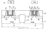
図1に、第1実施形態の半導体装置の概略構成図を示す。図1に示す半導体装置10は、Planar型構造を有するn型のFET(Field effect transistor)領域(以下、Nfet領域)とp型のFET(Field effect transistor)領域(以下、Nfet領域)とからなり、一方のゲート電極にオフセットスペーサが形成された構成である。なお、以下の説明では、半導体装置の第1導電型をp型とし、第2導電型をn型として説明する。
<1. First Embodiment of Semiconductor Device>
FIG. 1 shows a schematic configuration diagram of the semiconductor device of the first embodiment. A
図1に示す半導体装置10は、例えば、シリコン基板等からなる半導体基体11に、活性領域を区画する酸化シリコン等からなる素子分離12が形成されている。そして、Nfet領域の活性領域にはNウェル領域13が形成され、Pfet領域の活性領域にはPウェル領域14が形成されている。
In the
Nfet領域では、半導体基体11上に、HK絶縁層15及びNfet用WF(work function)メタル層17を介して埋め込み金属層18が形成されている。また、Pfet領域では、半導体基体11上に、HK絶縁層15、Pfet用WF(work function)メタル層16、及び、Nfet用WF(work function)メタル層17を介して埋め込み金属層18が形成されている。
半導体装置10では、Pfet用WFメタル層16又はNfet用WFメタル層17と、埋め込み金属層18とからなるメタルゲート電極が形成されている。
In the Nfet region, a buried
In the
HK絶縁層15は、酸化シリコンよりも誘電率の高い高誘電率層(High−k絶縁層)である。高誘電率層としては、HfO、HfSiO、LaO、ZrO、ZrSiO、TaO、TiO、BaSrTiO、BaTiO、StTiO、YO、AlO、及び、PbScTaO等を用いることができる。また、HK絶縁層15と酸化シリコン膜とを併用してゲート絶縁膜を構成してもよい。
埋め込み金属層18は、純金属材料、合金又は金属化合物からなり、例えば、Ti、Al、Cu及びW、又は、これらの金属を含む合金等からなる。
The
The buried
Nfet領域及びPfet領域では、埋め込み金属層18の側壁に、サイドウォールスペーサ21が形成されている。また、Pfet領域では、メタルゲート電極のサイドウォールスペーサ21の内壁に、オフセットスペーサ19が形成されている。このため、Pfet領域では、サイドウォールスペーサ21の内壁側から、オフセットスペーサ19、HK絶縁層15、Pfet用WFメタル層16及びNfet用WFメタル層17からなる多層体を有する。そして、この多層体で囲まれた内側に埋め込み金属層18が形成されている。
サイドウォールスペーサ21は、SiN、SiO2等からなり、単数又は複数の層により形成されている。また、オフセットスペーサ19には、SiN、SiO2等が用いられる。
The
オフセットスペーサ19は、Nfet領域とPfet領域とで、それぞれのゲート長を調整するために形成されている。
Nfet領域とPfet領域とは、サイドウォールスペーサの開口部が同じ大きさで形成されることが好ましい。これは、微細なパターンを加工する場合には、製造容易性の為にパターニングを一定で規則正しく設計することが望まれているためである。サイドウォールスペーサの開口部の大きさは、リソグラフィ工程におけるゲート電極のパターニングにより決定されるため、同一パターンであることが好ましい。特に、ゲート電極を形成する場合において、ゲート長方向の長さが微細化されている。このため、ゲート電極のゲート長方向の長さをNfet領域とPfet領域とで同じ長さに形成することで、リソグラフィ工程における負担を軽減することができる。
しかし、Nfet領域とPfet領域とで、リソグラフィ工程を同一パターンで行うと、それぞれの拡散層プロファイルに合わせたゲート長の最適化ができない。そこで、サイドウォールスペーサ開口部内に、オフセットスペーサ19を形成し、開口部の大きさを調整する。サイドウォールスペーサ21の内壁にオフセットスペーサ19が形成されていることにより、開口部内でWFメタル層16が形成される範囲を調整することができる。このため、ゲート長を任意の長さで最適化することができる。
The offset
The Nfet region and the Pfet region are preferably formed with the same size of the opening of the side wall spacer. This is because when a fine pattern is processed, it is desired to design the pattern regularly and regularly for ease of manufacturing. Since the size of the opening of the side wall spacer is determined by patterning of the gate electrode in the lithography process, the same pattern is preferable. In particular, when the gate electrode is formed, the length in the gate length direction is miniaturized. For this reason, by forming the gate electrode in the gate length direction to the same length in the Nfet region and the Pfet region, the burden on the lithography process can be reduced.
However, when the lithography process is performed in the same pattern in the Nfet region and the Pfet region, the gate length cannot be optimized in accordance with each diffusion layer profile. Therefore, an offset
図1に示す半導体装置10では、オフセットスペーサ19を備えるPfet領域の方が、オフセットスペーサ19を備えないNfet領域よりもゲート長が小さくなる。なお、オフセットスペーサは、Pfet領域のみに形成する場合だけでなく、Pfet領域とNfet領域との両方に形成されていてもよい。Pfet領域とNfet領域との両方にオフセットスペーサを形成する場合、Pfet領域とNfet領域とのオフセットスペーサの厚さは特に限定されない。例えば、Pfet領域とNfet領域とにおいて、それぞれ同じ厚さのオフセットスペーサを形成してもよく、また、それぞれ異なる厚さのオフセットスペーサを形成してもよい。特に、Pfet領域とNfet領域とにおいて、それぞれのMOSでゲート長を最適化するためにオフセットスペーサの厚さを適宜調整することが好ましい。
In the
埋め込み金属層18の両側であり、サイドウォールスペーサ21の直下の半導体基体11には、P型の不純物拡散領域であるソース・ドレイン23、又は、N型の不純物拡散領域であるソース・ドレイン24が形成されている。ソース・ドレイン23,24には、図示しない、LDD(Lightly Doped Drain)及びHaloが形成されている。また、サイドウォールスペーサ21から露出したソース・ドレイン23,24の表層は、シリサイド化されている。ソース・ドレイン23,24のシリサイドは、例えばコバルトシリサイド、ニッケルシリサイド又は白金シリサイド等からなる。
A source /
上記の第1実施形態の半導体装置では、メタルゲート電極及びWFメタル層の側面にオフセットスペーサが形成されている。このため、オフセットスペーサの厚さを変えることにより、ゲート長を任意に設定することができる。従って、リソグラフィ工程において同一パターンにダミーゲート電極及びサイドウォールスペーサを形成した場合にも、各領域において最適化したゲート長を有する半導体装置を構成することができる。 In the semiconductor device of the first embodiment, offset spacers are formed on the side surfaces of the metal gate electrode and the WF metal layer. For this reason, the gate length can be arbitrarily set by changing the thickness of the offset spacer. Therefore, even when the dummy gate electrode and the sidewall spacer are formed in the same pattern in the lithography process, a semiconductor device having an optimized gate length in each region can be configured.
〈2.第1実施形態の半導体装置の製造方法〉
次に、第1実施形態の半導体装置の製造方法について説明する。
[素子分離形成]
まず、シリコン基板からなる半導体基体11上に、SiO2、Si3N4を順次形成する。そして、活性領域を形成する部分に、レジストパターニングを行う。形成したレジストパターンをマスクにして、Si3N4、SiO2、及び、半導体基体11を順次エッチングし、トレンチ(トレンチ領域)を形成する。このとき、半導体基体11のトレンチの深さが350〜400nmになるまでエッチングを行う。Si3N4パターン領域が活性化領域となり、トレンチ領域がフィールド酸化膜となる。
<2. Manufacturing Method of Semiconductor Device of First Embodiment>
Next, a method for manufacturing the semiconductor device of the first embodiment will be described.
[Element isolation formation]
First, SiO 2 and Si 3 N 4 are sequentially formed on a
この後、トレンチ領域を、SiO2で埋め込む。例えば、高密度プラズマCVD等を用いることにより、段差被覆性が良好で緻密な膜を形成することができる。そして、CMP(Chemical Mechanical Polish)により表面を平坦化する。Si3N4領域では、Si3N4上のSiO2膜が除去できるまで、CMPによる研磨を行う。 Thereafter, the trench region is filled with SiO 2 . For example, a dense film with good step coverage can be formed by using high density plasma CVD or the like. Then, the surface is flattened by CMP (Chemical Mechanical Polish). In the Si 3 N 4 region, polishing by CMP is performed until the SiO 2 film on the Si 3 N 4 can be removed.
次に、Si3N4を、例えば、熱リン酸により除去し、活性領域を形成する。
活性領域を形成する部分の表面に、例えば10nmのSiO2(犠牲酸化膜)を形成する。Nfetを形成する領域に、Pwell領域の形成やパンチスルーの阻止を目的とした埋め込み層を形成するイオン注入、及び、閾値電圧(Vth)調整のためのイオン注入を行い、Nfetのチャネル領域を形成する。また、Pfetを形成する領域に、Nwell領域の形成及びパンチスルーの阻止を目的とした埋め込み層を形成するイオン注入、及び、閾値電圧(Vth)調整のためのイオン注入を行い、Pfetのチャネル領域を形成する。
以上の工程により、図2Aに示すように、半導体基体11に、Nウェル領域13とPウェル領域14、及び、両領域を区分する素子分離12を形成する。
Next, Si 3 N 4 is removed by, for example, hot phosphoric acid to form an active region.
For example, 10 nm of SiO 2 (sacrificial oxide film) is formed on the surface of the portion where the active region is to be formed. In the region where Nfet is formed, ion implantation for forming a buried layer for the purpose of forming a Pwell region and preventing punch-through and ion implantation for adjusting a threshold voltage (Vth) are performed to form an Nfet channel region. To do. In addition, ion implantation for forming a buried layer for the purpose of forming an Nwell region and preventing punch-through and ion implantation for adjusting a threshold voltage (Vth) are performed in a region for forming Pfet, and a channel region for Pfet is formed. Form.
Through the above steps, as shown in FIG. 2A, an
[ダミーゲート形成]
次に、図2Bに示すように、半導体基体11のNウェル領域13上とPウェル領域14上とに、ダミーゲート電極を形成する。
まず、活性領域を形成する際に半導体基体11上に設けた犠牲酸化膜を、フッ化水素(HF)溶液で剥離する。剥離後、ドライ酸化(O2、700℃)によりゲート絶縁膜26を1〜3nm程度形成する。酸化ガスとしては、例えば、ドライO2の他に、H2/O2、N2O、NOの混合ガスを用いることができる。また、ファーナスアニール(Furnace Anneal)処理や、ラピッドサーマルアニール(Rapid Thermal Anneal,RTA)処理を用いることも可能である。
[Dummy gate formation]
Next, as shown in FIG. 2B, dummy gate electrodes are formed on the
First, the sacrificial oxide film provided on the
次に、CVD法等を用いて、ダミーゲート電極材料層を形成する。ダミーゲート電極材料層は、ゲート絶縁膜26上に、例えば、ポリシリコン又はアモルファスシリコンを50〜100nm堆積して形成する。続いて、ハードマスクとしてSi3N4をLP−CVD(Low Pressure-Chemical Vaper Deposition)法を用いて、例えば50〜100nm程度堆積する。堆積後、リソグラフィを用いてSi3N4ハードマスクに電極のパターンを形成した後、このハードマスクパターンを用いてゲート絶縁膜26とダミーゲート電極材料層に異方性エッチングを行う。ダミーゲート電極材料層をパターニングすることにより、図2Bに示すように、半導体基体11上に、ゲート絶縁膜26とダミーゲート電極25を形成する。
ダミーゲート電極のパターンを、Nfet領域とPfet領域とで同じ形状に形成する。微細なパターンを加工する場合には、リソグラフィ工程での製造容易性の為に、パターニングを一定で規則正しく設計することが望まれている。このため、Nfet領域とPfet領域とにおいて、ダミーゲート電極を同じパターンで形成することにより、リソグラフィ工程での負担を軽減することができる。特に、ゲート電極を形成する場合において、ゲート長方向の長さが微細化されるため、Nfet領域とPfet領域とにおいて、ダミーゲート電極のゲート長方向の長さを同じパターンで形成することが好ましい。
Next, a dummy gate electrode material layer is formed using a CVD method or the like. The dummy gate electrode material layer is formed by depositing, for example, polysilicon or amorphous silicon on the
The dummy gate electrode pattern is formed in the same shape in the Nfet region and the Pfet region. In the case of processing a fine pattern, it is desired to design the pattern regularly and regularly for ease of manufacturing in the lithography process. Therefore, by forming the dummy gate electrode with the same pattern in the Nfet region and the Pfet region, the burden on the lithography process can be reduced. In particular, when the gate electrode is formed, the length in the gate length direction is miniaturized. Therefore, it is preferable to form the dummy gate electrode in the same length in the gate length direction in the Nfet region and the Pfet region. .
[拡散領域形成]
次に、図2Cに示すように、ダミーゲート電極25の側壁にサイドウォールスペーサ21を形成し、Nウェル領域13にP型のソース・ドレイン23、Pウェル領域14にN型のソース・ドレイン24を形成する。
[Diffusion region formation]
Next, as shown in FIG. 2C,
まず、Pfet領域に、BF2 +を3〜5keV、5〜20×1014/cm2でイオン注入し、PLDD領域を形成する。また、Nfet領域にAs+を5〜10keV、5〜20×1014/cm2でイオン注入し、NLDD領域を形成する。 First, BF 2 + is ion-implanted into the Pfet region at 3 to 5 keV and 5 to 20 × 10 14 / cm 2 to form a PLDD region. Further, As + is ion-implanted into the Nfet region at 5 to 10 keV and 5 to 20 × 10 14 / cm 2 to form an NLDD region.
また、短チャネル効果を抑制する為に、LDD形成と同時に、ソース・ドレインにウェルよりも不純物濃度を高めた、所謂halo注入を行う。例えば、Nfet領域には、Bを12keV、3×10¹³/cm2、45°で4分割して斜めイオン注入する。また、Pfet領域にはAsを、70keV、2×1013、45°で4分割して斜めイオン注入する。 In addition, in order to suppress the short channel effect, so-called halo implantation is performed at the same time as the LDD formation, in which the impurity concentration is higher than that of the well in the source / drain. For example, in the Nfet region, B is divided into four at 12 keV, 3 × 10 13 / cm 2 , 45 °, and oblique ion implantation is performed. Further, As is implanted into the Pfet region by dividing into four at 70 keV, 2 × 10 13 , and 45 °, and oblique ion implantation.
[サイドウォールスペーサ形成]
次に、ダミーゲート電極25の側壁に、サイドウォールスペーサ21を形成する。
プラズマCVDにより、ダミーゲート電極25を覆って半導体基体11上に、Si3N4を50〜150nm堆積する。この後、異方性エッチングを行い、Si3N4層をエッチバックすることによりダミーゲート電極25の側壁にサイドウォールスペーサ21を形成する。このとき、ダミーゲート電極25のハードマスクであるSi3N4を残存させる。
[Sidewall spacer formation]
Next,
Si 3 N 4 is deposited to a thickness of 50 to 150 nm on the
[拡散領域形成]
次に、Nウェル領域13にBF2 +を5〜10keV、1〜2×10¹⁵/cm2でイオン注入を行い、P型のソース・ドレイン23を形成する。また、Pウェル領域14にAs+を40〜50keV、1〜2×1015/cm2でイオン注入を行い、N型のソース・ドレイン24を形成する。イオン注入後、RTA(高速アニール装置)により、1000℃、5sの条件で不純物の活性化を行ない、図2Cに示すMOSFETを形成する。
[Diffusion region formation]
Next, BF 2 + is ion-implanted into the
MOSFETを形成後、所謂サリサイド技術を用いて、ソース・ドレイン23,24を低抵抗化する。例えば、半導体基体11上にNiをスパッタにより6〜8nm堆積する。RTAを300〜500、10sの条件で行い、ソース・ドレイン23,24のSi上のみシリサイド化(NiSi)を行う。シリサイド化後、H2SO4/H2O2など薬液によって未反応Niを除去する。
次に、図示しないコンタクトエッチングストッパとしてSiNを10〜100nm形成する。これは、トランジスタにおいてNMOSとPMOSとに別々の機械的ストレスをかけるよう、それぞれに2種類のSiNを個別に形成することも可能である。
さらに、ダミーゲート電極25及びサイドウォールスペーサ21を覆って、半導体基体11上に、層間絶縁層22としてSiO2を100〜1000nm程度堆積する。そして、図3Dに示すように、CMP法により平坦化を行うことでダミーゲート電極25上部を露出する。
After the MOSFET is formed, the resistance of the source / drains 23 and 24 is reduced by using a so-called salicide technique. For example, 6 to 8 nm of Ni is deposited on the
Next, 10 to 100 nm of SiN is formed as a contact etching stopper (not shown). It is also possible to form two types of SiN individually for each so that the NMOS and PMOS are subjected to different mechanical stresses in the transistor.
Further, SiO 2 is deposited to a thickness of about 100 to 1000 nm as the
[ダミーゲート除去]
次に、図3Eに示すように、ダミーゲート電極25を除去し、サイドウォールスペーサ21の内側を開口する。ダミーゲート電極25の除去は、ポリシリコン又はアモルファスシリコンからなる場合には、ドライエッチング法又はTMAH(水酸化テトラメチルアンモニウム水溶液)を使ったウェットエッチング法により行う。このとき、ダミーゲート電極25の下部にゲート絶縁膜26として形成されているSiO2も、ウェットエッチング法等を用いて取り除く。
[Dummy gate removal]
Next, as shown in FIG. 3E, the
[オフセットスペーサ形成]
次に、図3Fに示すように、Pfet領域において、サイドウォールスペーサ21の内壁側に、オフセットスペーサ19を形成する。
まず、半導体基体11上の全面に、オフセットスペーサ材料を1〜20nmの範囲で形成する。そして、オフセットスペーサ材料層を異方性エッチングによりエッチバックし、ダミーゲート除去後の溝内壁にオフセットスペーサ19を形成する。オフセットスペーサ材料には、SiN、SiO2等を用いる。
オフセットスペーサ19形成後、半導体基体11上の全面にレジスト層を形成し、リソグラフィによりNfet領域のダミーゲート除去後の溝を開口するレジストパターンを形成する。そして、HF溶液を用いたウェットエッチング法等を行い、Nfet領域のサイドウォールスペーサ21の内壁側に形成されたオフセットスペーサを除去する。例えば、オフセットスペーサ19をSiO2で形成する場合には、エッチバック等により層間絶縁層22の上部も、オフセットスペーサ材料層と同時に10nm程度エッチングされるが、この程度のエッチング量であれば、半導体装置の構成として特に問題は発生しない。
[Offset spacer formation]
Next, as shown in FIG. 3F, an offset
First, an offset spacer material is formed in the range of 1 to 20 nm on the entire surface of the
After the offset
また、例えば、上述のダミーゲート除去工程において、ダミーゲート電極25のみを除去し、ゲート絶縁膜15を残存させる。そして、オフセットスペーサ形成工程において、SiNを用いてダミーゲート電極25上を含む半導体基体11上の全面にオフセットスペーサ材料層を形成する。さらに、オフセットスペーサ材料層を異方性エッチングによりエッチバックし、Nfet領域のオフセットスペーサをエッチングする。Pfet領域にオフセットスペーサ19を形成した後、ゲート絶縁膜26を除去する。
上述の方法では、サイドウォールスペーサをSiNで形成することにより、オフセットスペーサ材料層をエッチングする際に、層間絶縁層22の上部のエッチングを防ぐことができる。
また、オフセットスペーサ材料層のエッチング時に、ダミーゲート電極を除去した後の溝内で半導体基体11の表面が露出していないため、エッチングによる半導体基体11への損傷を抑えることができる。
Further, for example, in the above-described dummy gate removing step, only the
In the above-described method, by forming the sidewall spacers with SiN, etching of the upper portion of the interlayer insulating
In addition, since the surface of the
[HK絶縁層形成]
次に、図4Gに示すように、HK絶縁層15によりゲート絶縁膜を形成する。
半導体基体11の全面に、ALD(Atomic Layer Deposition)法等を用いてHK絶縁層15を形成する。HK絶縁層15は、例えば、HfO、HfSiO、LaO、ZrO、ZrSiO、TaO、TiO、BaSrTiO、BaTiO、StTiO、YO、AlO、及び、PbScTaO等を用いて形成する。また、HK絶縁層15として、主に下地としてSiO2を含む場合がある。この場合には、プラズマ酸化等を用いてSiO2を形成する。
[HK insulation layer formation]
Next, as shown in FIG. 4G, a gate insulating film is formed by the
The
[WFメタル層形成]
HK絶縁層15を形成後、WF(work function)メタル層を形成する。WFメタル層により、単一又はNfet領域とPfet領域とで別個のメタル電極が形成される。以下、Nfet領域とPfet領域とに異なるWFメタル層を形成する場合を説明する。
[WF metal layer formation]
After forming the
まず、Pfet用WFメタル層16を先に形成する。
図4Gに示すように、半導体基体11の全面においてHK絶縁層15上に、PFET用WFメタル層16を1〜20nmの範囲でCVD、PVD又はALD法を用いて形成する。Pfet用WFメタル層16は、最適な仕事関数が5.2eVであり、この値に近い材料を用いる。例えば、Ru、Pd、Pt、Co、Ni及びMoを含む合金、若しくは、酸化物、TiN等を用いる。
First, the Pfet
As shown in FIG. 4G, the PFET
次に、Pfet用WFメタル層16をNfet領域からドライ又はウェットエッチング法により取り除く。このとき、Nfet領域にあるHK絶縁層15は除去せずに残す。例えば、Pfet領域のPfet用WFメタル層16を残存させる部分にレジストパターン等を形成し、このレジストパターンをマスクとして、Nfet領域のPfet用WFメタル層16をエッチングする。Pfet用WFメタル層16としてTiNを形成した場合には、例えばアンモニア過酸化水素水を用いてPfet用WFメタル層16をNfet領域から取り除く。
Next, the Pfet
次に、図4Hに示すように、HK絶縁層15及びPfet用WFメタル層16上に、Nfet用WFメタル層17を1〜20nmの範囲でCVD、PVD又はALD法を用いて形成する。Nfet用WFメタル層17は、最適な仕事関数が4.0eVであり、この値に近い材料を用いる。例えば、Hf、Zr、Ti、Ta及びAlを含む合金、若しくは、炭化物、HfSi等を用いる。
Next, as shown in FIG. 4H, the Nfet
[ゲートメタル埋め込み]
Pfet用WFメタル層16及びNfet用WFメタル層を形成後、図4Iに示すように、ダミーゲート除去後の溝内に低抵抗ゲート材料を埋め込み、埋め込み金属層18を形成する。低抵抗ゲート材料としては、例えば、Ti、Al、Cu及びW、又は、これらの金属を含む合金等を用いる。
埋め込み金属層18は、上述のように、ダミーゲート電極を除去した溝内に、オフセットスペーサ19や、HK絶縁層15等を形成した後に、低抵抗ゲート材料を埋め込んで低抵抗ゲート材料層を形成する。そして、CMP法を用いて、層間絶縁層22上の低抵抗ゲート材料層、Nfet用WFメタル層17、Pfet用WFメタル層16及びHK絶縁層15を除去し、平坦化する。つまり、埋め込み金属層18の形成と同時に、層間絶縁層22上に連続して形成されていた、Nfet用WFメタル層17、Pfet用WFメタル層16及びHK絶縁層15を除去し、溝内にのみ残存させる。
[Embedded gate metal]
After forming the Pfet
As described above, the buried
この工程により、ダミーゲート除去後の溝内にのみ低抵抗ゲート材料を残存させて、埋め込み金属層18を形成する。また、この工程において、Nfet用WFメタル層17、Pfet用WFメタル層16及び埋め込み金属層18からメタルゲート電極が形成される。
By this step, the buried
以上の工程により、図1に示す半導体装置10を製造することができる。この製造方法によれば、従来のGate−lastの製造方法に対し、オフセットスペーサ19をNfet領域から除去するためのリソグラフィ工程を1工程追加するのみで、第1実施形態の半導体装置を製造することができる。
Through the above steps, the
〈3.半導体装置の第2実施形態〉
図5に、第2実施形態の半導体装置の概略構成図を示す。図5に示す半導体装置20では、上述の図1に示す第1実施形態の半導体装置10と同様の構成については、同じ符号を付して詳細な説明を省略する。
<3. Second Embodiment of Semiconductor Device>
FIG. 5 is a schematic configuration diagram of the semiconductor device according to the second embodiment. In the
図5に示す半導体装置20は、シリコン基板等からなる半導体基体11に、活性領域を区画する酸化シリコン等からなる素子分離12が形成されている。そして、Nfet領域の活性領域にはNウェル領域13が形成されており、Pfet領域の活性領域にはPウェル領域14が形成されている。
In a
Nfet領域では、半導体基体11上に、HK絶縁層15及びNfet用WF(work function)メタル層17を介して埋め込み金属層18が形成されている。また、Pfet領域では、半導体基体11上に、HK絶縁層15、Pfet用WF(work function)メタル層16、及び、Nfet用WF(work function)メタル層17を介して埋め込み金属層18が形成されている。
半導体装置20では、Pfet用WFメタル層16又はNfet用WFメタル層17と、埋め込み金属層18とからメタルゲート電極が形成されている。
In the Nfet region, a buried
In the
HK絶縁層15は、酸化シリコンよりも誘電率の高い高誘電率層(High−k絶縁層)である。高誘電率層としては、HfO、HfSiO、LaO、ZrO、ZrSiO、TaO、TiO、BaSrTiO、BaTiO、StTiO、YO、AlO、及び、PbScTaO等が挙げられる。また、HK絶縁層15と酸化シリコン膜とを併用してゲート絶縁膜を構成してもよい。
埋め込み金属層18は、純金属材料、合金又は金属化合物からなり、例えば、Ti、Al、Cu及びW、又は、これらの金属を含む合金等からなる。
The
The buried
Nfet領域及びPfet領域では、埋め込み金属層18の側壁に、サイドウォールスペーサ21が形成されている。また、Pfet領域では、埋め込み金属層18の側壁部分において、HK絶縁層15とPfet用WFメタル層16との間にオフセットスペーサ19が形成されている。このため、Pfet領域では、サイドウォールスペーサ21の内壁側から、HK絶縁層15、オフセットスペーサ19、Pfet用WFメタル層16及びNfet用WFメタル層17からなる多層体を有する。そして、この多層体で囲まれた内側に埋め込み金属層18が形成されている。
サイドウォールスペーサ21は、SiN、SiO2等からなり、単数又は複数の層により形成されている。また、オフセットスペーサ19には、SiN、SiO2等が用いられる。
The
Pfet領域では、Pfet用WFメタル層16が形成される範囲によりゲート長が決定される。このため、HK絶縁層15の内壁に、オフセットスペーサ19を介してPfet用WFメタル層16を形成することにより、Pfet用WFメタル層16の形成範囲を制御することができる。オフセットスペーサ19を任意の厚さに設定することにより、サイドウォールスペーサ21の開口部内のPfet用WFメタル層16の形成範囲を任意の大きさにすることができる。このため、サイドウォールスペーサ21内の開口部の大きさに依存せずに、任意のゲート長を設定することができる。
なお、オフセットスペーサは、図5に示すように、Pfet領域のみに形成する場合だけでなく、Pfet領域とNfet領域との両方に形成されていてもよい。そして、Pfet領域とNfet領域とで、オフセットスペーサの厚さを変えることで、それぞれのゲート長を最適化することも可能である。
In the Pfet region, the gate length is determined by the range in which the Pfet
In addition, as shown in FIG. 5, the offset spacer may be formed not only in the Pfet region but also in both the Pfet region and the Nfet region. It is also possible to optimize the respective gate lengths by changing the thickness of the offset spacer between the Pfet region and the Nfet region.
埋め込み金属層18の両側であって、サイドウォールスペーサ21の直下における半導体基体11には、P型の不純物拡散領域であるソース・ドレイン23、又は、N型の不純物拡散領域であるソース・ドレイン24が形成されている。ソース・ドレイン23,24には、図示しない、LDD及びHaloが形成されている。また、サイドウォールスペーサ21から露出したソース・ドレイン23,24の表層は、シリサイド化されている。ソース・ドレイン23,24のシリサイドは、例えばコバルトシリサイド、ニッケルシリサイド又は白金シリサイド等からなる。
A source /
上記の第2実施形態の半導体装置では、埋め込み金属層及びWFメタル層の側面と、HK絶縁層の側面との間にオフセットスペーサが形成されている。このため、オフセットスペーサの厚さを変えることにより、WFメタル層の形成範囲を制御することができる。このため、オフセットスペーサによりゲート長を任意に設定することができる。従って、リソグラフィ工程において同一パターンにダミーゲート電極を形成した場合にも、各領域において最適化したゲート長を有する半導体装置を構成することができる。 In the semiconductor device of the second embodiment, offset spacers are formed between the side surfaces of the buried metal layer and the WF metal layer and the side surface of the HK insulating layer. For this reason, the formation range of the WF metal layer can be controlled by changing the thickness of the offset spacer. For this reason, the gate length can be arbitrarily set by the offset spacer. Therefore, even when the dummy gate electrodes are formed in the same pattern in the lithography process, a semiconductor device having an optimized gate length in each region can be configured.
〈4.第2実施形態の半導体装置の製造方法〉
次に、第2実施形態の半導体装置の製造方法について説明する。
第2実施形態の半導体装置の製造方法では、上述の第1実施形態の半導体製造方法における図3E示すダミーゲート電極の除去工程までは、同様に行うことができる。このため、以下の説明では、ダミーゲート電極の除去工程以降の製造方法について説明する。
<4. Manufacturing Method of Semiconductor Device of Second Embodiment>
Next, a method for manufacturing the semiconductor device of the second embodiment will be described.
In the manufacturing method of the semiconductor device of the second embodiment, the steps up to the dummy gate electrode removal step shown in FIG. 3E in the semiconductor manufacturing method of the first embodiment described above can be similarly performed. For this reason, in the following description, the manufacturing method after the dummy gate electrode removal step will be described.
[HK絶縁層形成]
図6Aに示すように、サイドウォールスペーサ21の内壁側にダミーゲート除去後の溝が形成され、さらに、層間絶縁層22、ソース・ドレイン23,24、Nウェル領域13及びPウェル領域14が形成された半導体基体11を準備する。
[HK insulation layer formation]
As shown in FIG. 6A, a trench after the dummy gate is removed is formed on the inner wall side of the
そして、図6Bに示すように、Nfet領域及びPfet領域において、サイドウォールスペーサ21の内壁側、及び層間絶縁層22上を含む半導体基体11全面にHK絶縁層15を形成する。
HK絶縁層15は、ALD(Atomic Layer Deposition)法等を用いて形成する。HK絶縁層15は、例えば、HfO、HfSiO、LaO、ZrO、ZrSiO、TaO、TiO、BaSrTiO、BaTiO、StTiO、YO、AlO、及び、PbScTaO等を用いて形成する。また、HK絶縁層15の下地にSiO2を形成してゲート絶縁膜とする場合がある。この場合には、プラズマ酸化等を用いてSiO2を形成する。
Then, as shown in FIG. 6B, in the Nfet region and the Pfet region, the
The
[オフセットスペーサ形成]
次に、HK絶縁層15上の全面にオフセットスペーサ材料を1〜20nmの範囲で形成する。そして、オフセットスペーサ材料層を異方性エッチングによりエッチバックすることで、図6Cに示すように、ダミーゲート除去後の溝内壁にのみオフセットスペーサ20を形成する。ここでは、Nfet領域とPfet領域との両領域において、ダミーゲート除去後の溝内壁にオフセットスペーサ19が形成される。オフセットスペーサ材料には、SiN、SiO2等を用いる。
[Offset spacer formation]
Next, an offset spacer material is formed in the range of 1 to 20 nm on the entire surface of the
[WFメタル層形成]
Nfet領域とPfet領域との両領域、又は、一方の領域にオフセットスペーサ19を形成後、Pfet用WF(work function)メタル層16を形成する。
図7Dに示すように、半導体基体11の全面において、HK絶縁層15上にPfet用WFメタル層16を1〜20nmの範囲でCVD、PVD又はALD法を用いて形成する。Pfet用WFメタル層16は、最適な仕事関数が5.2eVであり、この値に近い材料を用いる。例えば、Ru、Pd、Pt、Co、Ni及びMoを含む合金、若しくは、酸化物、TiN等を用いる。
[WF metal layer formation]
After forming the offset
As shown in FIG. 7D, the Pfet
次に、Pfet用WFメタル層16をNfet領域からドライ又はウェットエッチング法により取り除く。このとき、Nfet領域にあるHK絶縁層15は除去せずに残す。例えば、Pfet領域のPfet用WFメタル層16を残存させる部分にレジストパターンを形成し、このレジストパターンをマスクとして、Nfet領域のPfet用WFメタル層16をエッチングする。Pfet用WFメタル層16としてTiNを形成した場合には、アンモニア過酸化水素水を用いてPfet用WFメタル層16をNfet領域から取り除く。
Next, the Pfet
さらに、Nfet領域からPfet用WFメタル層16を除去した後、Nfet領域のダミーゲート除去後の溝内壁に形成されたオフセットスペーサ19を除去する。例えば、Pfet用WFメタル層16をマスクとして、Nfet領域に形成されたオフセットスペーサ19を、HF溶液を用いたウェットエッチング法などにより取り除く。これにより、パターンマスクを形成するリソグラフィ等の工程の追加を必要とせずに、Nfet領域のオフセットスペーサ19を除去し、Pfet領域のみにオフセットスペーサ19を残存させることができる。
Further, after removing the Pfet
次に、図7Eに示すように、HK絶縁層15及びPfet用WFメタル層16上に、Nfet用WFメタル層17を1〜20nmの範囲でCVD、PVD又はALD法を用いて形成する。
Nfet用WFメタル層17は、最適な仕事関数が4.0eVであり、この値に近い材料を用いる。例えば、Hf、Zr、Ti、Ta及びAlを含む合金、若しくは、炭化物、HfSi等を用いる。
Next, as shown in FIG. 7E, an Nfet
The Nfet
[ゲートメタル埋め込み]
Pfet用WFメタル層16及びNfet用WFメタル層17を形成後、図7Fに示すように、ダミーゲート除去後の溝内に低抵抗ゲート材料を埋め込み、埋め込み金属層18を形成する。低抵抗ゲート材料としては、例えば、Ti、Al、Cu及びW、又は、これらの金属を含む合金等を用いる。
埋め込み金属層18は、上述のように、ダミーゲート電極を除去後、HK絶縁層15、オフセットスペーサ19、Pfet用WFメタル層16及びNfet用WFメタル層17上、並びに、溝内を埋め込む低抵抗ゲート材料層を形成する。そして、CMP法を用いて、層間絶縁層22上の低抵抗ゲート材料層、Nfet用WFメタル層17、Pfet用WFメタル層16及びHK絶縁層15を除去し、平坦化する。
[Embedded gate metal]
After the Pfet
As described above, the buried
この工程により、ダミーゲート除去後の溝内にのみ低抵抗ゲート材料を残存させて、埋め込み金属層18を形成する。また、この工程において、Nfet用WFメタル層17、Pfet用WFメタル層16及び埋め込み金属層18からなるメタルゲート電極が形成される。
By this step, the buried
以上の工程により、図5に示す半導体装置20を製造することができる。この製造方法では、Pfet領域のオフセットスペーサの除去を、Pfet用WFメタル層の除去と連続して行うことができる。このため、第1実施形態の製造方法に比べて、オフセットスペーサ19をNfet領域から除去するためのリソグラフィ工程を行う必要がなく、製造工程を簡略化して半導体装置を製造することができる。
Through the above steps, the
〈5.半導体装置の第3実施形態〉
図8に、第3実施形態の半導体装置の概略構成図を示す。図8に示す半導体装置30では、上述の図1に示す第1実施形態の半導体装置10と同様の構成については、同じ符号を付して詳細な説明を省略する。
<5. Third Embodiment of Semiconductor Device>
FIG. 8 shows a schematic configuration diagram of the semiconductor device of the third embodiment. In the
図8に示す半導体装置30は、シリコン基板等からなる半導体基体11に、活性領域を区画する酸化シリコン等からなる素子分離12が形成されている。そして、NMOS領域の活性領域にはNウェル領域13が形成されており、PMOS領域の活性領域にはPウェル領域14が形成されている。
In the
Nfet領域では、半導体基体11上に、HK絶縁層15及びNfet用WF(work function)メタル層17を介して埋め込み金属層18が形成されている。また、Pfet領域では、半導体基体11上に、HK絶縁層15、及び、Pfet用WF(work function)メタル層16を介して埋め込み金属層18が形成されている。
半導体装置30では、Pfet用WFメタル層16又はNfet用WFメタル層17と、埋め込み金属層18とからメタルゲート電極が形成されている。
In the Nfet region, a buried
In the
HK絶縁層15は、酸化シリコンよりも誘電率の高い高誘電率層(High−k絶縁層)である。高誘電率層としては、HfO、HfSiO、LaO、ZrO、ZrSiO、TaO、TiO、BaSrTiO、BaTiO、StTiO、YO、AlO、及び、PbScTaO等が挙げられる。また、HK絶縁層15と酸化シリコン膜とを併用してゲート絶縁膜を構成してもよい。
埋め込み金属層18は、純金属材料、合金又は金属化合物からなり、例えば、Ti、Al、Cu及びW、又は、これらの金属を含む合金等からなる。
The
The buried
Nfet領域及びPfet領域では、埋め込み金属層18の側壁に、サイドウォールスペーサ21が形成されている。また、Pfet領域では、埋め込み金属層18の側壁部分において、HK絶縁層15とPfet用WFメタル層16との間にオフセットスペーサ19が形成されている。サイドウォールスペーサ21は、SiN、SiO2等からなり、単数又は複数の層により形成されている。また、オフセットスペーサ19には、SiN、SiO2等が用いられる。
Nfet領域では、埋め込み金属層18の両側のサイドウォールスペーサ21の直下の半導体基体11に、N型の不純物拡散領域であるソース・ドレイン24が形成されている。また、Pfet領域では、埋め込み金属層18の両側のサイドウォールスペーサ21の直下に、エピタキシャル層により形成されたレイズドソース・ドレイン部27と、P型の不純物拡散領域であるソース・ドレイン23が形成されている。ソース・ドレイン23,24には、図示しない、LDD及びHaloが形成されている。
In the Nfet region, the source /
また、サイドウォールスペーサ21から露出したソース・ドレイン23,24、及び、レイズドソース・ドレイン部27の表層は、シリサイド化されている。これらのシリサイドは、例えばコバルトシリサイド、ニッケルシリサイド又は白金シリサイド等からなる。
Further, the surface layers of the source / drains 23 and 24 and the raised source /
上記の第3実施形態の半導体装置30のNfet領域では、埋め込み金属層18の底面にのみHK絶縁層15とNfet用WFメタル層17が形成されている。また、Pfet領域では、埋め込み金属層18底面にのみHK絶縁層15とPfet用WFメタル層16が形成されている。そして、HK絶縁層15とPfet用WFメタル層上において、メタルゲート電極とサイドウォールスペーサ21との間にオフセットスペーサ19が形成されている。
In the Nfet region of the
第3実施形態の半導体装置3のPfet領域では、Pfet用WFメタル層16上にオフセットスペーサ19が形成されているため、Pfet用WFメタル層16の形成範囲に影響がない。このため、オフセットスペーサ19の形成によるゲート長の調整ができない。しかし、Pfet用WFメタル層16とメタルゲート電極とから逆T字型ゲートを形成することにより、ゲート側壁フリンジング容量を低減させることができる。これは、特に、最近のストレス技術、例えば、PMOSにembedded SiGeを適用する場合、及び、NMOSにembedded SiCを適用する場合において、ゲート拡散層間の容量の増加を改善することができる。
In the Pfet region of the semiconductor device 3 of the third embodiment, since the offset
〈6.第3実施形態の半導体装置の製造方法〉
次に、第3実施形態の半導体装置の製造方法について説明する。
[素子分離形成]
まず、図9Aに示すように、半導体基体11に、Nウェル領域13とPウェル領域14とを区分する素子分離12を形成する。これは、図2Aに示す素子分離形成工程と同様に行うことができる。
<6. Manufacturing Method of Semiconductor Device of Third Embodiment>
Next, a method for manufacturing the semiconductor device of the third embodiment will be described.
[Element isolation formation]
First, as shown in FIG. 9A, an
[HK絶縁層、WFメタル及びダミーゲート形成]
まず、活性領域を形成する際に半導体基体11上に設けた犠牲酸化膜をフッ化水素(HF)溶液で剥離する。剥離後、HK絶縁層をALD(Atomic Layer Deposition)法等により形成する。HK絶縁層は、HfO、HfSiO、LaO、ZrO、ZrSiO、TaO、TiO、BaSrTiO、BaTiO、StTiO、YO、AlO、及び、PbScTaO等を用いて形成する。また、HK絶縁層として、主に下地としてSiO2を含む場合がある。この場合には、プラズマ酸化等を用いてSiO2を形成する。
[HK insulating layer, WF metal and dummy gate formation]
First, the sacrificial oxide film provided on the
次に、HK絶縁層15上にWF(work function)メタル層を形成する。WFメタル層により、単一又はNMOSとPMOSとで別個のメタル電極を形成する。以下、NMOSとPMOSとに異なる種類のWFメタル層を形成する場合について説明する。
Next, a WF (work function) metal layer is formed on the
Nfet領域において、HK絶縁層15上にNfet用WFメタル層17を形成する。また、Pfet領域において、HK絶縁層15上にPfet用WFメタル層16を形成する。
Pfet用WFメタル層16及びNfet用WFメタル層17は、例えば、TiNを1〜20nmの範囲でCVD法、PVD法、又は、ALD法により形成する。Pfet用WFメタル層16は、最適な仕事関数が5.2eVであり、この値に近い材料を用いる。例えば、Ru、Pd、Pt、Co、Ni及びMoを含む合金、若しくは、酸化物、TiN等を用いる。また、Nfet用WFメタル層17は、最適な仕事関数が4.0eVであり、この値に近い材料を用いる。例えば、Hf、Zr、Ti、Ta及びAlを含む合金、若しくは、炭化物、HfSi等を用いる。
In the Nfet region, the Nfet
The Pfet
Pfet用WFメタル層16及びNfet用WFメタル層17を形成後、ダミーゲート電極材料層を形成する。ダミーゲート電極材料層は、Pfet用WFメタル層16及びNfet用WFメタル層17上に、CVD法等を用いてポリシリコン又はアモルファスシリコンを50〜100nm堆積して形成する。続いて、ハードマスクとしてSi3N4をLP−CVD法を用いて、例えば50〜100nm程度堆積する。堆積後、リソグラフィを用いてSi3N4ハードマスクに電極のパターンを形成した後、このハードマスクパターンを用いてHK絶縁層15、Pfet用WFメタル層16及びNfet用WFメタル層17と、ダミーゲート電極材料層とに異方性エッチングを行う。ダミーゲート電極材料層をパターニングすることにより、図9Bに示すように、半導体基体11上のNfet領域に、HK絶縁層15、Nfet用WFメタル層17及びダミーゲート電極25を形成する。また、半導体基体11上のPfet領域に、HK絶縁層15、Pfet用WFメタル層16及びダミーゲート電極25を形成する。
After forming the Pfet
[レイズドソース・ドレイン形成]
次に、図9Cに示すように、ダミーゲート電極25の側壁にサイドウォールスペーサ21を形成する。そして、Nウェル領域13にP型のソース・ドレイン23を形成し、Pウェル領域14にN型のソース・ドレイン24と、レイズドソース・ドレイン部27とを形成する。
[Raised source / drain formation]
Next, as shown in FIG. 9C,
まず、Pfet領域に、レイズドソース・ドレイン部27を形成する。
まず、半導体基体11上にダミーゲート電極25を覆うSiN層を形成する。そして、Pfet領域を開口するレジストパターンを形成する。レジスト開口部からSiN層を異方性エッチングでエッチバックし、ダミーゲート電極25の側壁にダミーサイドウォールスペーサを形成する。
ダミーサイドウォールスペーサ形成後、レジスト開口部の半導体基体11をエッチングした後、SiGeを選択成長させて、エピタキシャル成長層(epi層)を形成する。
SiGeからなるepi層を形成した後、ダミーサイドウォールスペーサとPfet領域以外に残存するSiN層を取り除き、レイズドソース・ドレイン部27を形成する。
First, a raised source /
First, an SiN layer that covers the
After forming the dummy sidewall spacer, the
After the epi layer made of SiGe is formed, the remaining SiN layer other than the dummy sidewall spacer and the Pfet region is removed, and the raised source /
[拡散領域形成]
次に、PMOS領域に、BF2 +を3〜5keV、5〜20×1014/cm2でイオン注入し、PLDD領域を形成する。また、NMOS領域にAs+を5〜10keV、5〜20×1014/cm2でイオン注入し、NLDD領域を形成する。
[Diffusion region formation]
Next, BF 2 + is ion-implanted into the PMOS region at 3 to 5 keV and 5 to 20 × 10 14 / cm 2 to form a PLDD region. Further, As + is ion-implanted into the NMOS region at 5 to 10 keV and 5 to 20 × 10 14 / cm 2 to form an NLDD region.
また、短チャネル効果を抑制する為に、LDD形成と同時に、ソース・ドレインにウェルよりも不純物濃度を高めた、所謂halo注入を行う。例えば、Nfet領域には、Bを12keV、3×10¹³/cm2、45°で4分割して斜めイオン注入する。また、Pfet領域にはAsを、70keV、2×1013、45°で4分割して斜めイオン注入する。 In addition, in order to suppress the short channel effect, so-called halo implantation is performed at the same time as the LDD formation, in which the impurity concentration is higher than that of the well in the source / drain. For example, in the Nfet region, B is divided into four at 12 keV, 3 × 10 13 / cm 2 , 45 °, and oblique ion implantation is performed. Further, As is implanted into the Pfet region by dividing into four at 70 keV, 2 × 10 13 , and 45 °, and oblique ion implantation.
[サイドウォールスペーサ形成]
次に、ダミーゲート電極25の側壁に、サイドウォールスペーサ21を形成する。
プラズマCVDにより、ダミーゲート電極25を覆って半導体基体11上に、Si3N4を50〜150nm堆積する。この後、異方性エッチングを行い、Si3N4層をエッチバックすることによりダミーゲート電極25の側壁にサイドウォールスペーサ21を形成する。このとき、ダミーゲート電極25のハードマスクであるSi3N4を残存させる。
[Sidewall spacer formation]
Next,
Si 3 N 4 is deposited to a thickness of 50 to 150 nm on the
[拡散領域形成]
次に、Nウェル領域13にBF2 +を5〜10keV、1〜2×10¹⁵/cm2でイオン注入を行い、P型のソース・ドレイン23を形成する。BF2 +のイオン注入は、BによるP型領域がレイズドソース・ドレイン部27の全域に形成されるように行う。また、Pウェル領域14にAs+を40〜50keV、1〜2×10¹⁵/cm2でイオン注入を行い、N型のソース・ドレイン24を形成する。イオン注入後、RTA(高速アニール装置)により、1000℃、5sの条件で不純物の活性化を行ない、図9Cに示すMOSFETを形成する。
[Diffusion region formation]
Next, BF 2 + is ion-implanted into the
MOSFETを形成後、所謂サリサイド技術を用いて、ソース・ドレイン23,24を低抵抗化する。例えば、半導体基体11上にNiをスパッタにより6〜8nm堆積する。RTAを300〜500、10sの条件で行い、ソース・ドレイン23,24のSi上のみシリサイド化(NiSi)を行う。シリサイド化後、H2SO4/H2O2など薬液によって未反応Niを除去する。
次に、図示しないコンタクトエッチングストッパとしてSiNを10〜100nm形成する。これは、トランジスタにNMOSとPMOStpに別々の機械的ストレスをかけるよう、それぞれに2種類のSiNを個別に形成することも可能である。
さらに、ダミーゲート電極25、サイドウォールスペーサ21、及び、レイズドソース・ドレイン部27を覆って、半導体基体11上に層間絶縁層22としてSiO2を100〜1000nm程度堆積する。そして、CMP法を用いて平坦化を行うことでダミーゲート電極25上部を露出する。
After the MOSFET is formed, the resistance of the source / drains 23 and 24 is reduced by using a so-called salicide technique. For example, 6 to 8 nm of Ni is deposited on the
Next, 10 to 100 nm of SiN is formed as a contact etching stopper (not shown). It is also possible to form two types of SiN separately for each so that the NMOS and PMOStp are subjected to different mechanical stresses.
Further, SiO 2 is deposited to a thickness of about 100 to 1000 nm as an
[ダミーゲート除去]
次に、図10Dに示すように、ダミーゲート電極25を除去し、サイドウォールスペーサ21の内側を開口する。ダミーゲート電極25の除去は、ポリシリコン又はアモルファスシリコンからなる場合には、ドライエッチング法あるいはTMAH(水酸化テトラメチルアンモニウム水溶液)を使ったウェットエッチング法により行う。
[Dummy gate removal]
Next, as shown in FIG. 10D, the
[オフセットスペーサ形成]
次に、図10Eに示すように、Pfet領域のサイドウォールスペーサ21の内壁側において、Pfet用WFメタル層上に、オフセットスペーサ19を形成する。
ダミーゲート除去後の溝の底部には、Pfet用WFメタル層16又はNfet用WFメタル層17が存在する。このダミーゲート除去後の溝を覆って、オフセットスペーサ材料を1〜20nmの範囲で形成する。そして、異方性エッチングによりエッチバックし、ダミーゲート除去後の溝内壁にオフセットスペーサを形成する。オフセットスペーサ材料には、SiN、SiO2等を用いる。
その後、HF溶液を用いたウェットエッチング法等を用いて、Nfet領域からオフセットスペーサを取り除く。
[Offset spacer formation]
Next, as shown in FIG. 10E, an offset
The Pfet
Thereafter, the offset spacer is removed from the Nfet region by using a wet etching method using an HF solution.
[ゲートメタル埋め込み]
オフセットスペーサ19を形成後、図10Fに示すように、ダミーゲート除去後の溝内に低抵抗ゲート材料を埋め込み、埋め込み金属層18を形成する。低抵抗ゲート材料としては、例えば、Ti、Al、Cu及びW、又は、これらの金属を含む合金等を用いる。
埋め込み金属層18は、ダミーゲート電極を除去した溝内において、オフセットスペーサ19の形成後、Pfet用WFメタル層16又はNfet用WFメタル層17上に低抵抗ゲート材料を埋め込んで低抵抗ゲート材料層を形成する。そして、CMP法を用いて、層間絶縁層22上の低抵抗ゲート材料層を除去して平坦化する。この工程により、ダミーゲート除去後の溝内にのみ低抵抗ゲート材料を残存させて、埋め込み金属層18を形成する。
[Embedded gate metal]
After the offset
The buried
以上の工程により、図8に示す半導体装置30を製造することができる。この製造方法によれば、オフセットスペーサ19よりも先にPfet用WFメタル層16をダミーゲート除去後の溝内に形成する。このため、オフセットスペーサ19の形成目的は、ゲート長の調整ではなく、ゲート側壁フリンジング容量を低減である。メタルゲート電極とサイドウォールスペーサ21との間にオフセットスペーサ19を形成することにより、メタルゲート電極がPfet用WFメタル層16よりも狭い面積に形成され、Pfet用WFメタル層16とメタルゲート電極とにより逆T字型ゲートが形成される。このように、逆T字型ゲートを形成することにより、最近のストレス技術、例えば、PMOSにembedded SiGeを適用する場合、及び、NMOSにembedded SiCを適用する場合において、ゲート拡散層容量の増加を改善することができる。
Through the above steps, the
〈7.半導体装置の第4実施形態〉
図11に、第4実施形態の半導体装置の概略構成図を示す。図11Aに、第4実施形態の半導体装置40の平面図を示し、この半導体装置40のA−A´線断面図を図11Bに示す。図11に示す半導体装置40は、fin型構造を有するNfet領域とPfet領域とからなる。そして、一方のゲート電極にオフセットスペーサが形成された構成である。以下の説明では、半導体装置の第1導電型をp型とし、第2導電型をn型として説明する。
<7. Fourth Embodiment of Semiconductor Device>
FIG. 11 is a schematic configuration diagram of the semiconductor device of the fourth embodiment. FIG. 11A shows a plan view of the
図11Aに示す半導体装置40は、例えば、Pfet領域とNfet領域とに、それぞれ起立した薄い半導体層(フィン)43が形成されている。そして、フィン42とフィン43のチャネル領域がゲート電極44等で覆われている。このように、フィン42及びフィン43のチャネル領域に対し、左右両側面からゲート電極44で挟み込む構成のfin型の電界効果トランジスタ(finFET)が形成されている。例えば、図示しないシリコン基板等からなる半導体基体上に酸化絶縁層41を形成し、この酸化絶縁層41に起立した薄い半導体層(フィン)42,43が形成される。そして、Pfet領域のフィン42はP型の不純物が拡散されたソース・ドレインを有し、Nfet領域のフィン43はN型の不純物が拡散されたソース・ドレインを有する。
In the
次に、図11Bに示す半導体装置40のゲート電極44の構造を説明する。
ゲート電極44は、上述のフィン42,43のチャネル領域を、一方の側面から対向する他方の側面までを覆う、コ字状に形成されている。半導体装置40のゲート電極は、Pfet領域とNfet領域とでそれぞれ異なる構成を有する。
Next, the structure of the
The
Pfet領域では、酸化絶縁層41上に、HK絶縁層45及びPfet用WF(work function)メタル層46、及び、Nfet用WF(work function)メタル層47を介して埋め込み金属層48が形成されている。また、Nfet領域では、酸化絶縁層41上に、HK絶縁層45及びNfet用WF(work function)メタル層47を介して埋め込み金属層48が形成されている。
半導体装置40では、Pfet用WFメタル層46又はNfet用WFメタル層47と、埋め込み金属層48とからメタルゲート電極44が形成されている。
In the Pfet region, a buried
In the
HK絶縁層45は、酸化シリコンよりも誘電率の高い高誘電率層(High−k絶縁層)である。高誘電率層としては、HfO、HfSiO、LaO、ZrO、ZrSiO、TaO、TiO、BaSrTiO、BaTiO、StTiO、YO、AlO、及び、PbScTaO等が挙げられる。また、HK絶縁層45と酸化シリコン膜とを併用してゲート絶縁膜を構成してもよい。
埋め込み金属層48は、純金属材料、合金又は金属化合物からなり、例えば、Ti、Al、Cu及びW、又は、これらの金属を含む合金等からなる。
The
The embedded
Nfet領域及びPfet領域では、埋め込み金属層48の側壁に、サイドウォールスペーサ51が形成されている。また、Pfet領域では、HK絶縁層45とサイドウォールスペーサ51の内壁の下層部に、オフセットスペーサ49が形成されている。このため、Pfet領域では、サイドウォールスペーサ21の内壁側から、オフセットスペーサ49、HK絶縁層45、Pfet用WFメタル層46及びNfet用WFメタル層47からなる多層体を有する。そして、この多層体で囲まれた内側に埋め込み金属層48が形成されている。
サイドウォールスペーサ51は、SiN、SiO2等からなり、単数又は複数の層により形成されている。また、オフセットスペーサ49には、SiN、SiO2等が用いられる。
In the Nfet region and the Pfet region,
The
オフセットスペーサ49は、サイドウォールスペーサ51内壁の下部にのみ形成されている。また、オフセットスペーサ49は、フィン42の上部よりも高い位置まで形成されている。従って、フィン42が形成されている部分では、HK絶縁層及びPfet用WFメタル層46とサイドウォールスペーサ51とは、オフセットスペーサ49を介してのみフィン42と接続される。
The offset
サイドウォールスペーサの開口部の大きさはリソグラフィ工程におけるパターニングにより形成されるため、同一パターンであることが好ましい。
これは、微細なパターンを加工する場合には、製造容易性の為、一定で規則正しいパターニングの設計が要求されているためである。このため、Nfet領域とPfet領域とで、サイドウォールスペーサの開口部が同じ大きさで形成されることが好ましい。しかし、Nfet領域とPfet領域とで、サイドウォールスペーサ開口部を同じにすると、それぞれの拡散層プロファイルに合わせたゲート長の最適化ができない。
そこで、サイドウォールスペーサ開口部内に、オフセットスペーサ19を形成し、開口部の大きさを調整する。WFメタル層46とサイドウォールスペーサ51との間にオフセットスペーサ49が形成されていることにより、Pfet領域のゲート長を調整することができる。そして、開口部内において、オフセットスペーサ49により、Pfet用WFメタル層46が形成される範囲は調整されるため、ゲート長を任意の長さに最適化することができる。
Since the size of the opening of the sidewall spacer is formed by patterning in the lithography process, it is preferable that the side wall spacer has the same pattern.
This is because, when processing a fine pattern, a constant and regular patterning design is required for manufacturability. For this reason, it is preferable that the opening portion of the sidewall spacer is formed in the same size in the Nfet region and the Pfet region. However, if the sidewall spacer openings are the same in the Nfet region and the Pfet region, the gate length cannot be optimized in accordance with each diffusion layer profile.
Therefore, an offset
また、fin型の半導体装置の場合には、ゲート電極底部とゲート側壁形状とがゲート長に影響する。このため、ゲート電極が形成されるサイドウォールスペーサの内壁がテーパ状となる場合やラフネスが存在する場合には、ゲート長にばらつきが発生し、最適化が困難となる。
これに対し、第4実施形態の半導体装置では、サイドウォールスペーサ51の内壁側、特に、サイドウォールスペーサ51とHK絶縁層45との間、又は、HK絶縁層45とWFメタル層46との間にオフセットスペーサ49を形成する。この構造により、例えば、サイドウォールスペーサ51の内壁にラフネスが存在する場合には、オフセットスペーサ49によりフィン42が形成されたサイドウォールスペーサ51内壁を平坦化することができる。また、例えば、サイドウォールスペーサ51の内壁がテーパ状であった場合にも、オフセットスペーサ49を形成することにより、フィン42の形成部分の内壁を垂直にしてゲート長を調整することができる。
In the case of a fin-type semiconductor device, the gate electrode bottom and the gate sidewall shape affect the gate length. For this reason, when the inner wall of the sidewall spacer on which the gate electrode is formed is tapered or when there is roughness, the gate length varies, making optimization difficult.
On the other hand, in the semiconductor device of the fourth embodiment, the inner wall side of the
なお、オフセットスペーサは、図11に示すように、Pfet領域のみに形成する場合だけでなく、Nfet領域のみ、又は、Pfet領域とNfet領域との両方に形成されていてもよい。この場合には、Pfet領域とNfet領域とで、オフセットスペーサの厚さを変えることで、それぞれのゲート長を最適化することもできる。 In addition, as shown in FIG. 11, the offset spacer may be formed not only in the Pfet region but also in the Nfet region only, or in both the Pfet region and the Nfet region. In this case, the gate length can be optimized by changing the thickness of the offset spacer between the Pfet region and the Nfet region.
上記の第4実施形態の半導体装置で示すように、上述の第1実施形態及び第2実施形態のようなPlanar型構造の半導体装置のゲート電極構造を、fin型構造の半導体装置に適用することができる。そして、オフセットスペーサの厚さを変えることにより、ゲート長の最適化が可能となる。従って、リソグラフィ工程において同一パターンにダミーゲート電極及びサイドウォールスペーサを形成した場合にも、各領域において最適化したゲート長を有する半導体装置を構成することができる。 As shown in the semiconductor device of the fourth embodiment, the gate electrode structure of the planar type semiconductor device as in the first and second embodiments is applied to the fin type semiconductor device. Can do. The gate length can be optimized by changing the thickness of the offset spacer. Therefore, even when the dummy gate electrode and the sidewall spacer are formed in the same pattern in the lithography process, a semiconductor device having an optimized gate length in each region can be configured.
〈8.第4実施形態の半導体装置の製造方法〉
次に、第4実施形態の半導体装置の製造方法について説明する。第4実施形態の半導体装置の製造方法は、上述の第1実施形態の半導体装置の製造方法をfin型半導体装置に適用する以外は、同様の工程により行うことができる。以下の説明では、第1実施形態の半導体装置の製造方法と同様の工程については詳細な説明を省略して記載する。
<8. Manufacturing Method of Semiconductor Device of Fourth Embodiment>
Next, a method for manufacturing the semiconductor device of the fourth embodiment will be described. The manufacturing method of the semiconductor device of the fourth embodiment can be performed by the same process except that the manufacturing method of the semiconductor device of the first embodiment described above is applied to the fin type semiconductor device. In the following description, detailed description of steps similar to those of the semiconductor device manufacturing method of the first embodiment will be omitted.
[フィン形成]
まず、図12Aに示すように、酸化絶縁層41上にフィン42,43を形成する。
公知の方法により、Pfet領域にフィン42を形成する。また、Nfet領域にフィン43を形成する。例えば、シリコン等の半導体層を堆積した後、P型又はN型の不純物をイオン注入してソース・ドレインを形成し、所定のフィン形状にエッチングする。
[Fin formation]
First, as shown in FIG. 12A,
The
[ダミーゲート形成]
次に、酸化絶縁層41のNfet領域上とPfet領域上とに、ゲート絶縁膜とダミーゲート電極を形成する。
まず、フィン42,43の表面に、例えばドライ酸化(O2、700℃)によりゲート絶縁膜を1〜3nm程度形成する。そして、CVD法等を用いて、ダミーゲート電極材料層を形成する。ダミーゲート電極材料層は、酸化絶縁層41上に、例えば、ポリシリコン又はアモルファスシリコンを50〜100nm堆積して形成する。堆積後、リソグラフィを用いてレジストパターンを形成した後、このレジストをマスクとして、ダミーゲート電極材料層に異方性エッチングを行う。ダミーゲート電極材料層をパターニングすることにより、図12Aに示すように、酸化絶縁層41上に、ダミーゲート電極53を形成する。
[Dummy gate formation]
Next, a gate insulating film and a dummy gate electrode are formed on the Nfet region and the Pfet region of the
First, a gate insulating film of about 1 to 3 nm is formed on the surfaces of the
[サイドウォールスペーサ形成]
次に、ダミーゲート電極53の側壁に、サイドウォールスペーサ51を形成する。
プラズマCVDにより、酸化絶縁層41上にダミーゲート電極53を覆って、Si3N4を50〜150nm堆積する。この後、異方性エッチングを行い、Si3N4層をエッチバックすることによりダミーゲート電極53の側壁にサイドウォールスペーサ51を形成する。
[Sidewall spacer formation]
Next,
Si 3 N 4 is deposited to a thickness of 50 to 150 nm on the
さらに、ダミーゲート電極53及びサイドウォールスペーサ51を覆って、酸化絶縁層41上に層間絶縁層52としてSiO2を100〜1000nm程度堆積する。そして、図12Bに示すように、CMPにより平坦化を行うことでダミーゲート電極53の上面を露出する。
Further, covering the
[ダミーゲート除去]
次に、図12Cに示すように、ダミーゲート電極53を除去し、サイドウォールスペーサ51の内側を開口し、フィン42,43を露出させる。ダミーゲート電極53の除去は、ポリシリコン又はアモルファスシリコンからなる場合には、ドライエッチング法あるいはTMAH(水酸化テトラメチルアンモニウム水溶液)を使ったウェットエッチング法により行う。このとき、ダミーゲート電極53の下部にゲート絶縁膜として形成されているSiO2も、ウェットエッチング法等を用いて除去する。
[Dummy gate removal]
Next, as shown in FIG. 12C, the
[オフセットスペーサ形成]
次に、図13Dに示すように、Pfet領域において、ダミーゲート除去後の溝内において、サイドウォールスペーサ51の内壁にオフセットスペーサ49を形成する。
まず、酸化絶縁層41上の全面、サイドウォールスペーサ51の内壁側開口部内、及び、露出されたフィン42,43上に、オフセットスペーサ材料を1〜20nmの範囲で形成する。オフセットスペーサ材料には、SiN、SiO2等を用いる。そして、オフセットスペーサ材料層を異方性エッチングによりエッチバックする。
オフセットスペーサ材料層のエッチバックでは、サイドウォールスペーサ51の開口部から露出するフィン42,43の側壁に形成されるオフセットスペーサ材料層が除去されるまで、オーバーエッチングを行う。このようにエッチングを行うことにより、フィン42,43の側壁に残存させずに、サイドウォールスペーサ51の内壁側のみにオフセットスペーサ49を形成することができる。
[Offset spacer formation]
Next, as shown in FIG. 13D, an offset
First, an offset spacer material is formed in the range of 1 to 20 nm on the entire surface of the
In the etch back of the offset spacer material layer, over-etching is performed until the offset spacer material layer formed on the sidewalls of the
このとき、上述のダミーゲート電極53及びサイドウォールスペーサ51は、フィンの2倍以上の高さで形成する必要がある。フィンの2倍以上の高さとすることにより、フィン42,43の側壁に形成されるオフセットスペーサ材料層が除去されるまで、オーバーエッチングを行った場合に、サイドウォールスペーサ51内壁側において、フィン42,43が形成されている高さ以上にオフセットスペーサ49が残存する。
また、上述の第1実施形態の半導体装置の製造方法と同様に、ダミーゲート除去工程において、ゲート絶縁膜の除去を行わず、オフセットスペーサ49の形成後にゲート絶縁膜を除去することも可能である。
At this time, it is necessary to form the
Further, as in the semiconductor device manufacturing method of the first embodiment described above, the gate insulating film can be removed after the offset
オフセットスペーサ49形成後、酸化絶縁層41上の全面にレジスト層を形成し、リソグラフィによりNfet領域のダミーゲート除去後の溝を開口するレジストパターンを形成する。そして、HF溶液等を用いたウェットエッチング法等を行い、Nfet領域のサイドウォールスペーサ51の内壁側に形成されたオフセットスペーサを除去する。
After the offset
[HK絶縁層形成]
次に、図13Eに示すように、HK絶縁層45によりゲート絶縁膜を形成する。
サイドウォールスペーサ51の内壁側開口部内を覆って層間絶縁層52の全面に、ALD(Atomic Layer Deposition)法等を用いてHK絶縁層45を用いて形成する。HK絶縁層45は、例えば、HfO、HfSiO、LaO、ZrO、ZrSiO、TaO、TiO、BaSrTiO、BaTiO、StTiO、YO、AlO、及び、PbScTaO等を用いて形成する。
[HK insulation layer formation]
Next, as illustrated in FIG. 13E, a gate insulating film is formed by the
The
[WFメタル層形成]
HK絶縁層45を形成後、WF(work function)メタル層を形成する。WFメタル層により、単一又はNMOSとPMOSとで別個のメタルゲート電極が形成される。以下、NMOSとPMOSとに異なるWFメタル層を形成する場合について説明する。
[WF metal layer formation]
After the
まず、Pfet用WFメタル層46を先に形成する。
図13Eに示すように、HK絶縁層45上に、Pfet用WFメタル層46を1〜20nmの範囲でCVD、PVD又はALD法を用いて形成する。Pfet用WFメタル層46は、最適な仕事関数が5.2eVであり、この値に近い材料を用いる。例えば、Ru、Pd、Pt、Co、Ni及びMoを含む合金、若しくは、酸化物、TiN等を用いる。
First, the Pfet
As shown in FIG. 13E, a
次に、Pfet用WFメタル層46をNfet領域からドライ又はウェットエッチング法により取り除く。このとき、Nfet領域にあるHK絶縁層45は除去せずに残す。例えば、Pfet領域のPfet用WFメタル層46を残存させる部分にレジストパターンを形成し、このレジストパターンをマスクとして、Nfet領域のPfet用WFメタル層46をエッチングする。Pfet用WFメタル層46としてTiNを形成した場合には、例えばアンモニア過酸化水素水を用いてPfet用WFメタル層46をNfet領域から取り除く。
Next, the Pfet
そして、HK絶縁層45及びPfet用WFメタル層46上に、Nfet用WFメタル層47を1〜20nmの範囲でCVD、PVD又はALD法を用いて形成する。Nfet用WFメタル層17は、最適な仕事関数が4.0eVであり、この値に近い材料を用いる。例えば、Hf、Zr、Ti、Ta及びAlを含む合金、若しくは、炭化物、HfSi等を用いる。
Then, the Nfet
[ゲートメタル埋め込み]
Pfet用WFメタル層46及びNfet用WFメタル層47を形成後、図13Fに示すように、ダミーゲート除去後の溝内に低抵抗ゲート材料を埋め込み、埋め込み金属層48を形成する。低抵抗ゲート材料としては、例えば、Ti、Al、Cu及びW、又は、これらの金属を含む合金等を用いる。
埋め込み金属層48は、上述のように、ダミーゲート電極を除去した溝内に、オフセットスペーサ49、HK絶縁層45、Pfet用WFメタル層46、及び、Nfet用WFメタル層47等の形成後、低抵抗ゲート材料を埋め込んで低抵抗ゲート材料層を形成する。そして、CMP法を用いて、層間絶縁層52上の低抵抗ゲート材料層、Nfet用WFメタル層47、Pfet用WFメタル層46及びHK絶縁層45を除去して平坦化する。
[Embedded gate metal]
After the Pfet
As described above, the buried
この工程により、ダミーゲート除去後の溝内にのみ低抵抗ゲート材料を残存させて、埋め込み金属層48を形成する。また、この工程において、埋め込み金属層48の形成と同時に、層間絶縁層52上に連続して形成されていた、Nfet用WFメタル層47、Pfet用WFメタル層46及びHK絶縁層45を除去し、溝内にのみ残存させる。
By this step, the buried
以上の工程により、図11に示す半導体装置40を製造することができる。この製造方法によれば、フィン型の半導体層を形成する工程と加えることで、第1実施形態と同様の製造工程により、本実施の形態のフィン型半導体装置を製造することができる。そして、オフセットスペーサをサイドウォールスペーサ内壁とWFメタル層との間に形成することによりゲート長の最適化が可能である。
Through the above steps, the
なお、第4実施形態の半導体装置では、第1実施形態と同様に、オフセットスペーサをサイドウォールスペーサ内壁とHK絶縁層との間に形成しているが、オフセットスペーサの形成位置は、サイドウォールスペーサ内壁とWFメタル層との間であれば特に限定されない。例えば、第2実施形態の半導体装置のように、サイドウォールスペーサ内壁側において、HK絶縁層とWFメタル層との間にオフセットスペーサを形成してもよい。
この場合には、図12Cを用いて説明したようにダミーゲート電極を除去した後、ダミーゲート除去後の溝内にHK絶縁層を形成する。そして、図13Dを用いて説明したようにHK絶縁層上にオフセットスペーサ材料層をフィンの2倍以上の高さで形成した後、オフセットスペーサ材料をエッチバックし、サイドウォールスペーサの内壁側のみにオフセットスペーサを形成する。さらに、図13E,Fを用いて説明したように、溝内にWFメタル層と埋め込み金属層を形成する。このように、第4実施形態の半導体装置の製造方法に、第2実施形態の半導体装置の製造方法を適用することで、HK絶縁層とWFメタル層との間にオフセットスペーサが形成されたフィン型の半導体装置を製造することができる。
In the semiconductor device of the fourth embodiment, as in the first embodiment, the offset spacer is formed between the inner wall of the sidewall spacer and the HK insulating layer. The offset spacer is formed at the side wall spacer. If it is between an inner wall and a WF metal layer, it will not specifically limit. For example, as in the semiconductor device of the second embodiment, an offset spacer may be formed between the HK insulating layer and the WF metal layer on the side wall spacer inner wall side.
In this case, as described with reference to FIG. 12C, after the dummy gate electrode is removed, an HK insulating layer is formed in the trench after the dummy gate is removed. Then, as described with reference to FIG. 13D, after the offset spacer material layer is formed on the HK insulating layer at a height of twice or more of the fin, the offset spacer material is etched back, and only on the inner wall side of the side wall spacer. An offset spacer is formed. Further, as described with reference to FIGS. 13E and 13F, a WF metal layer and a buried metal layer are formed in the groove. As described above, by applying the manufacturing method of the semiconductor device of the second embodiment to the manufacturing method of the semiconductor device of the fourth embodiment, the fin in which the offset spacer is formed between the HK insulating layer and the WF metal layer. Type semiconductor device can be manufactured.
なお、本発明は上述の実施形態例において説明した構成に限定されるものではなく、その他本発明構成を逸脱しない範囲において種々の変形、変更が可能である。 The present invention is not limited to the configuration described in the above-described embodiment, and various modifications and changes can be made without departing from the configuration of the present invention.
10,20,30,40,60 半導体装置、11,61 半導体基体、12 素子分離、13 Nウェル領域、14 Pウェル領域、15,45,65 HK絶縁層、16,46,66 Pfet用WFメタル層、17,47,67 Nfet用WFメタル層、18,48 埋め込み金属層、19,49 オフセットスペーサ、21,51,69 サイドウォールスペーサ、22,52,64 層間絶縁層、23,24 ソース・ドレイン、25,53,71 ダミーゲート電極、26,72 ゲート絶縁膜、27 レイズドソース・ドレイン部、41 酸化絶縁層、42,43 フィン、44,62,63 ゲート電極、68 メタルゲート電極
10, 20, 30, 40, 60 Semiconductor device, 11, 61 Semiconductor substrate, 12 Device isolation, 13 N well region, 14 P well region, 15, 45, 65 HK insulating layer, 16, 46, 66 Pfet WF metal Layer, 17, 47, 67 Nfet WF metal layer, 18, 48 buried metal layer, 19, 49 offset spacer, 21, 51, 69 sidewall spacer, 22, 52, 64 interlayer insulation layer, 23, 24 source /
Claims (15)
前記第1導電型のトランジスタ及び前記第2導電型のトランジスタは、
基体上に形成されたゲート絶縁膜と、
前記ゲート絶縁膜上に形成されたメタルゲート電極と、
前記メタルゲート電極の側壁に形成されたサイドウォールスペーサと、を有し、
前記ゲート絶縁膜が高誘電率材料からなり、
前記第1導電型のトランジスタ及び前記第2導電型のトランジスタのいずれか一方に、前記メタルゲート電極の側壁と前記サイドウォールスペーサの内壁との間にオフセットスペーサが形成されている、或いは、前記第1導電型のトランジスタと前記第2導電型のトランジスタとに厚さの異なるオフセットスペーサが形成されている
半導体装置。 A first conductivity type transistor and a second conductivity type transistor;
The first conductivity type transistor and the second conductivity type transistor are:
A gate insulating film formed on the substrate;
A metal gate electrode formed on the gate insulating film;
A sidewall spacer formed on the side wall of the metal gate electrode,
The gate insulating film is made of a high dielectric constant material,
In either one of the first conductivity type transistor and the second conductivity type transistor, an offset spacer is formed between a side wall of the metal gate electrode and an inner wall of the side wall spacer, or A semiconductor device in which offset spacers having different thicknesses are formed between a first conductivity type transistor and the second conductivity type transistor.
前記ゲート絶縁膜上に形成されたメタルゲート電極と、
前記メタルゲート電極の側壁に形成されたオフセットスペーサと、
前記オフセットスペーサを介して前記メタルゲート電極の側壁に形成されたサイドウォールスペーサと、を備え、
前記ゲート絶縁膜が高誘電率材料からなり、
前記ゲート絶縁膜が、前記メタルゲート電極の底部から前記サイドウォールスペーサの内壁まで連続して形成され、前記オフセットスペーサと前記サイドウォールスペーサとの間に前記ゲート絶縁膜が介在する
半導体装置。 A gate insulating film formed on the substrate;
A metal gate electrode formed on the gate insulating film;
An offset spacer formed on a side wall of the metal gate electrode;
A sidewall spacer formed on the sidewall of the metal gate electrode through the offset spacer,
The gate insulating film is made of a high dielectric constant material,
The semiconductor device, wherein the gate insulating film is continuously formed from the bottom of the metal gate electrode to the inner wall of the sidewall spacer, and the gate insulating film is interposed between the offset spacer and the sidewall spacer.
前記ゲート絶縁膜上に形成されたWFメタル層と、
前記WFメタル層上に形成された埋め込み金属層と、
前記WFメタル層上において、前記埋め込み金属層の側壁に形成されたオフセットスペーサと、
前記オフセットスペーサを介して前記埋め込み金属層の側壁に形成されたサイドウォールスペーサと、を備え、
前記ゲート絶縁膜が高誘電率材料からなる
半導体装置。 A gate insulating film formed on the substrate;
A WF metal layer formed on the gate insulating film;
A buried metal layer formed on the WF metal layer;
An offset spacer formed on a sidewall of the buried metal layer on the WF metal layer;
A sidewall spacer formed on a sidewall of the buried metal layer via the offset spacer,
A semiconductor device in which the gate insulating film is made of a high dielectric constant material.
前記第1導電型の半導体領域及び前記第2導電型の半導体領域において、
前記基体上にダミーゲート電極を形成する工程と、
前記ダミーゲート電極の側壁にサイドウォールスペーサを形成する工程と、
前記サイドウォールスペーサを埋め込み、かつ前記ダミーゲート電極の上面を露出させる層間絶縁層を形成する工程と、
前記ダミーゲート電極を除去する工程と、
前記第1導電型の半導体領域及び前記第2導電型の半導体領域のいずれか一方において、前記サイドウォールスペーサの内壁にオフセットスペーサを形成する、或いは、前記第1導電型の半導体領域と前記第2導電型の半導体領域とにおいて、前記サイドウォールスペーサの内壁に厚さの異なるオフセットスペーサを形成する工程と、
前記サイドウォールスペーサ内に露出する前記基体上に高誘電率材料からなるゲート絶縁膜を形成する工程と、
前記ゲート絶縁膜上にメタルゲート電極を形成する工程と、を有する
半導体装置の製造方法。 Forming a first conductivity type semiconductor region and a second conductivity type semiconductor region on a substrate;
In the first conductivity type semiconductor region and the second conductivity type semiconductor region,
Forming a dummy gate electrode on the substrate;
Forming a sidewall spacer on the side wall of the dummy gate electrode;
Forming an interlayer insulating layer that embeds the sidewall spacer and exposes the upper surface of the dummy gate electrode;
Removing the dummy gate electrode;
In any one of the first conductivity type semiconductor region and the second conductivity type semiconductor region, an offset spacer is formed on an inner wall of the sidewall spacer, or the first conductivity type semiconductor region and the second conductivity region are formed. A step of forming an offset spacer having a different thickness on the inner wall of the sidewall spacer in a conductive semiconductor region;
Forming a gate insulating film made of a high dielectric constant material on the substrate exposed in the sidewall spacer;
Forming a metal gate electrode on the gate insulating film. A method for manufacturing a semiconductor device.
前記ダミーゲート電極の側壁にサイドウォールスペーサを形成する工程と、
前記サイドウォールスペーサを埋め込み、かつ前記ダミーゲート電極の上面を露出させる層間絶縁層を形成する工程と、
前記ダミーゲート電極を除去する工程と、
前記サイドウォールスペーサ内に露出する前記基体上、及び、前記サイドウォールスペーサの内壁に高誘電率材料からなるゲート絶縁膜を形成する工程と、
前記ゲート絶縁膜の側壁部にオフセットスペーサを形成する工程と、
前記ゲート絶縁膜上及び前記オフセットスペーサの内壁側にメタルゲート電極を形成する工程と、を有する
半導体装置の製造方法。 Forming a dummy gate electrode on the substrate;
Forming a sidewall spacer on the side wall of the dummy gate electrode;
Forming an interlayer insulating layer that embeds the sidewall spacer and exposes the upper surface of the dummy gate electrode;
Removing the dummy gate electrode;
Forming a gate insulating film made of a high dielectric constant material on the substrate exposed in the sidewall spacer and on the inner wall of the sidewall spacer;
Forming an offset spacer on the side wall of the gate insulating film;
Forming a metal gate electrode on the gate insulating film and on the inner wall side of the offset spacer. A method for manufacturing a semiconductor device.
前記ゲート絶縁膜上にWFメタル層を形成する工程と、
前記WFメタル層上にダミーゲート電極を形成する工程と、
前記ダミーゲート電極の側壁にサイドウォールスペーサを形成する工程と、
前記サイドウォールスペーサを埋め込み、かつ前記ダミーゲート電極の上面を露出させる層間絶縁層を形成する工程と、
前記ダミーゲート電極を除去する工程と、
前記サイドウォールスペーサ内に露出する前記WFメタル層上、及び、前記サイドウォールスペーサの内壁にオフセットスペーサを形成する工程と、
前記ゲート絶縁膜上及び前記オフセットスペーサの内壁側に埋め込み金属層を形成する工程と、を有する
半導体装置の製造方法。 Forming a gate insulating film made of a dielectric material on a substrate;
Forming a WF metal layer on the gate insulating film;
Forming a dummy gate electrode on the WF metal layer;
Forming a sidewall spacer on the side wall of the dummy gate electrode;
Forming an interlayer insulating layer that embeds the sidewall spacer and exposes the upper surface of the dummy gate electrode;
Removing the dummy gate electrode;
Forming an offset spacer on the WF metal layer exposed in the sidewall spacer and on the inner wall of the sidewall spacer;
Forming a buried metal layer on the gate insulating film and on the inner wall side of the offset spacer. A method for manufacturing a semiconductor device.
Priority Applications (15)
| Application Number | Priority Date | Filing Date | Title |
|---|---|---|---|
| JP2010243251A JP2012099517A (en) | 2010-10-29 | 2010-10-29 | Semiconductor device and method of manufacturing the same |
| US13/278,809 US9059312B2 (en) | 2010-10-29 | 2011-10-21 | Semiconductor device and manufacturing method of semiconductor device |
| CN202010965994.6A CN112201626B (en) | 2010-10-29 | 2011-10-21 | Semiconductor devices |
| CN201810372654.5A CN108666273B (en) | 2010-10-29 | 2011-10-21 | Semiconductor device |
| CN201810390786.0A CN108470733B (en) | 2010-10-29 | 2011-10-21 | Method for manufacturing semiconductor device |
| CN201510969631.9A CN105448835B (en) | 2010-10-29 | 2011-10-21 | semiconductor device |
| CN201110322857.1A CN102456691B (en) | 2010-10-29 | 2011-10-21 | Semiconductor device and semiconductor device manufacturing method |
| CN201810372155.6A CN108735673B (en) | 2010-10-29 | 2011-10-21 | Semiconductor device with a plurality of semiconductor chips |
| US14/709,047 US9331077B2 (en) | 2010-10-29 | 2015-05-11 | Semiconductor device and manufacturing method of semiconductor device |
| US15/080,657 US9741814B2 (en) | 2010-10-29 | 2016-03-25 | Semiconductor device with fin transistors and manufacturing method of such semiconductor device |
| US15/588,072 US10373955B2 (en) | 2010-10-29 | 2017-05-05 | Semiconductor device with FIN transistors and manufacturing method of such semiconductor device |
| US16/443,319 US10811416B2 (en) | 2010-10-29 | 2019-06-17 | Semiconductor device with fin transistors and manufacturing method of such semiconductor device |
| US17/023,611 US11121133B2 (en) | 2010-10-29 | 2020-09-17 | Semiconductor device with fin transistors and manufacturing method of such semiconductor device |
| US17/399,222 US11824057B2 (en) | 2010-10-29 | 2021-08-11 | Semiconductor device with fin-type field effect transistor |
| US18/485,440 US12170282B2 (en) | 2010-10-29 | 2023-10-12 | Semiconductor device with fin transistors and manufacturing method of such semiconductor device |
Applications Claiming Priority (1)
| Application Number | Priority Date | Filing Date | Title |
|---|---|---|---|
| JP2010243251A JP2012099517A (en) | 2010-10-29 | 2010-10-29 | Semiconductor device and method of manufacturing the same |
Publications (1)
| Publication Number | Publication Date |
|---|---|
| JP2012099517A true JP2012099517A (en) | 2012-05-24 |
Family
ID=45995729
Family Applications (1)
| Application Number | Title | Priority Date | Filing Date |
|---|---|---|---|
| JP2010243251A Pending JP2012099517A (en) | 2010-10-29 | 2010-10-29 | Semiconductor device and method of manufacturing the same |
Country Status (3)
| Country | Link |
|---|---|
| US (8) | US9059312B2 (en) |
| JP (1) | JP2012099517A (en) |
| CN (6) | CN108470733B (en) |
Cited By (7)
| Publication number | Priority date | Publication date | Assignee | Title |
|---|---|---|---|---|
| KR20150008304A (en) * | 2013-07-12 | 2015-01-22 | 삼성전자주식회사 | Semiconductor device and fabricating method thereof |
| KR20150123143A (en) * | 2014-04-24 | 2015-11-03 | 타이완 세미콘덕터 매뉴팩쳐링 컴퍼니 리미티드 | Structure and method for finfet device |
| JP2017504205A (en) * | 2013-12-31 | 2017-02-02 | 日本テキサス・インスツルメンツ株式会社 | High k / metal gate CMOS transistor with TiN gate |
| US9966455B2 (en) | 2016-09-26 | 2018-05-08 | Renesas Electronics Corporation | Method for manufacturing a semiconductor device |
| KR20180048403A (en) * | 2016-11-01 | 2018-05-10 | 에이에스엠 아이피 홀딩 비.브이. | Methods for forming a semiconductor device and related semiconductor device structures |
| JP2019079907A (en) * | 2017-10-24 | 2019-05-23 | 東京エレクトロン株式会社 | Semiconductor device and CMOS transistor |
| CN110010453A (en) * | 2013-04-03 | 2019-07-12 | 意法半导体公司 | Method and apparatus for enhancing the mobility of electric charge carrier |
Families Citing this family (63)
| Publication number | Priority date | Publication date | Assignee | Title |
|---|---|---|---|---|
| JP2012099517A (en) * | 2010-10-29 | 2012-05-24 | Sony Corp | Semiconductor device and method of manufacturing the same |
| DE102011004322B4 (en) * | 2011-02-17 | 2012-12-06 | Globalfoundries Dresden Module One Llc & Co. Kg | A method of manufacturing a semiconductor device having self-aligned contact elements and an exchange gate electrode structure |
| US8445345B2 (en) | 2011-09-08 | 2013-05-21 | International Business Machines Corporation | CMOS structure having multiple threshold voltage devices |
| US8901665B2 (en) * | 2011-12-22 | 2014-12-02 | Taiwan Semiconductor Manufacturing Company, Ltd. | Gate structure for semiconductor device |
| CN103515207B (en) * | 2012-06-19 | 2016-08-10 | 中芯国际集成电路制造(上海)有限公司 | Oxide layer, HKMG structure median surface layer, MOS transistor forming method and MOS transistor |
| CN103681498B (en) * | 2012-09-12 | 2016-03-30 | 中芯国际集成电路制造(上海)有限公司 | A kind of manufacture method of semiconductor device |
| US9209182B2 (en) | 2012-12-28 | 2015-12-08 | Taiwan Semiconductor Manufacturing Company, Ltd. | Dummy metal gate structures to reduce dishing during chemical-mechanical polishing |
| CN103928330B (en) | 2013-01-11 | 2017-05-24 | 中芯国际集成电路制造(上海)有限公司 | Semiconductor structure and forming method thereof |
| US9412664B2 (en) * | 2013-05-06 | 2016-08-09 | International Business Machines Corporation | Dual material finFET on single substrate |
| US8872241B1 (en) * | 2013-05-20 | 2014-10-28 | International Business Machines Corporation | Multi-direction wiring for replacement gate lines |
| US20140357073A1 (en) * | 2013-06-04 | 2014-12-04 | Globalfoundries Inc. | Systems and methods for fabricating gate structures for semiconductor devices |
| KR102089682B1 (en) | 2013-07-15 | 2020-03-16 | 삼성전자 주식회사 | Semiconductor device and method for fabricating the same |
| CN104576386B (en) | 2013-10-14 | 2018-01-12 | 中国科学院微电子研究所 | A kind of FinFET and its manufacturing method |
| US9437711B2 (en) * | 2013-11-15 | 2016-09-06 | Globalfoundries Inc. | Methods of forming gate structures for semiconductor devices using a replacement gate technique and the resulting devices |
| US9455346B2 (en) | 2013-12-09 | 2016-09-27 | Taiwan Semiconductor Manufacturing Co., Ltd. | Channel strain inducing architecture and doping technique at replacement poly gate (RPG) stage |
| US9576952B2 (en) * | 2014-02-25 | 2017-02-21 | Globalfoundries Inc. | Integrated circuits with varying gate structures and fabrication methods |
| US9947772B2 (en) | 2014-03-31 | 2018-04-17 | Stmicroelectronics, Inc. | SOI FinFET transistor with strained channel |
| CN105244318B (en) * | 2014-07-09 | 2018-07-20 | 中芯国际集成电路制造(上海)有限公司 | A kind of semiconductor devices and its manufacturing method and electronic device |
| US9281372B2 (en) | 2014-07-17 | 2016-03-08 | Taiwan Semiconductor Manufacturing Company Ltd. | Metal gate structure and manufacturing method thereof |
| US9954112B2 (en) | 2015-01-26 | 2018-04-24 | Semiconductor Energy Laboratory Co., Ltd. | Semiconductor device and manufacturing method thereof |
| US9514997B2 (en) * | 2015-03-25 | 2016-12-06 | International Business Machines Corporation | Silicon-germanium FinFET device with controlled junction |
| CN106158637B (en) * | 2015-03-31 | 2019-04-26 | 中芯国际集成电路制造(上海)有限公司 | Fin field effect transistor and method of forming the same |
| US10504721B2 (en) | 2015-04-30 | 2019-12-10 | Taiwan Semiconductor Manufacturing Company, Ltd. | Staggered-type tunneling field effect transistor |
| US9397003B1 (en) | 2015-05-27 | 2016-07-19 | Globalfoundries Inc. | Method for forming source/drain contacts during CMOS integration using confined epitaxial growth techniques |
| US9559205B2 (en) * | 2015-05-29 | 2017-01-31 | Taiwan Semiconductor Manufacturing Company, Ltd. | Structure and formation method of semiconductor device structure |
| KR101785803B1 (en) * | 2015-05-29 | 2017-10-16 | 타이완 세미콘덕터 매뉴팩쳐링 컴퍼니 리미티드 | Structure and formation method of semiconductor device structure |
| US9330984B1 (en) * | 2015-07-08 | 2016-05-03 | International Business Machines Corporation | CMOS fin integration on SOI substrate |
| KR102350007B1 (en) * | 2015-08-20 | 2022-01-10 | 삼성전자주식회사 | Method for fabricating semiconductor device |
| US9711533B2 (en) * | 2015-10-16 | 2017-07-18 | Taiwan Semiconductor Manufacturing Company, Ltd. | FinFET devices having different source/drain proximities for input/output devices and non-input/output devices and the method of fabrication thereof |
| US9570450B1 (en) | 2015-11-19 | 2017-02-14 | International Business Machines Corporation | Hybrid logic and SRAM contacts |
| US10109627B2 (en) | 2016-03-08 | 2018-10-23 | Taiwan Semiconductor Manufacturing Co., Ltd. | Enlarging spacer thickness by forming a dielectric layer over a recessed interlayer dielectric |
| CN107170685B (en) * | 2016-03-08 | 2020-02-07 | 中芯国际集成电路制造(上海)有限公司 | Method for forming fin type transistor |
| US9613855B1 (en) | 2016-04-05 | 2017-04-04 | Globalfoundries Inc. | Methods of forming MIS contact structures on transistor devices in CMOS applications |
| US9831123B2 (en) * | 2016-04-05 | 2017-11-28 | Globalfoundries Inc. | Methods of forming MIS contact structures on transistor devices |
| US10079291B2 (en) * | 2016-05-04 | 2018-09-18 | Taiwan Semiconductor Manufacturing Co., Ltd. | Fin-type field effect transistor structure and manufacturing method thereof |
| EP3244447A1 (en) * | 2016-05-11 | 2017-11-15 | IMEC vzw | Method for forming a gate structure and a semiconductor device |
| US10147802B2 (en) * | 2016-05-20 | 2018-12-04 | Globalfoundries Inc. | FINFET circuit structures with vertically spaced transistors and fabrication methods |
| US10290654B2 (en) | 2016-05-20 | 2019-05-14 | Globalfoundries Inc. | Circuit structures with vertically spaced transistors and fabrication methods |
| CN107481932B (en) * | 2016-06-08 | 2020-08-07 | 中芯国际集成电路制造(上海)有限公司 | Method for manufacturing semiconductor structure |
| CN107516668B (en) | 2016-06-15 | 2020-04-24 | 中芯国际集成电路制造(北京)有限公司 | Semiconductor device and method for manufacturing the same |
| US12051589B2 (en) | 2016-06-28 | 2024-07-30 | Lam Research Corporation | Tin oxide thin film spacers in semiconductor device manufacturing |
| US9824893B1 (en) | 2016-06-28 | 2017-11-21 | Lam Research Corporation | Tin oxide thin film spacers in semiconductor device manufacturing |
| US10256143B2 (en) * | 2016-12-14 | 2019-04-09 | Taiwan Semiconductor Manufacturing Co., Ltd. | Replacement contacts |
| KR102722138B1 (en) | 2017-02-13 | 2024-10-24 | 램 리써치 코포레이션 | Method to create air gaps |
| US10546748B2 (en) | 2017-02-17 | 2020-01-28 | Lam Research Corporation | Tin oxide films in semiconductor device manufacturing |
| CN108807378A (en) * | 2017-05-05 | 2018-11-13 | 中芯国际集成电路制造(上海)有限公司 | Fin field effect pipe and forming method thereof |
| US10658486B2 (en) * | 2017-05-18 | 2020-05-19 | Taiwan Semiconductor Manufacutring Co., Ltd. | Mitigation of time dependent dielectric breakdown |
| CN107680993B (en) * | 2017-10-23 | 2019-12-24 | 深圳市华星光电半导体显示技术有限公司 | OLED panel and manufacturing method thereof |
| CN109904112B (en) * | 2017-12-11 | 2021-01-12 | 中芯国际集成电路制造(北京)有限公司 | Semiconductor device and method for manufacturing the same |
| CN111771264A (en) | 2018-01-30 | 2020-10-13 | 朗姆研究公司 | Tin oxide mandrel in patterning |
| CN108389897B (en) * | 2018-02-02 | 2021-01-22 | 上海华虹宏力半导体制造有限公司 | Gate spacer and method of forming the same |
| CN108493246A (en) * | 2018-02-09 | 2018-09-04 | 中国科学院微电子研究所 | Semiconductor device and manufacturing method thereof |
| US11987876B2 (en) | 2018-03-19 | 2024-05-21 | Lam Research Corporation | Chamfer-less via integration scheme |
| US11201152B2 (en) * | 2018-04-20 | 2021-12-14 | Globalfoundries Inc. | Method, apparatus, and system for fin-over-nanosheet complementary field-effect-transistor |
| CN108695259B (en) * | 2018-05-21 | 2020-11-24 | 上海华力集成电路制造有限公司 | Manufacturing method of MOS transistor with HKMG |
| US11011625B2 (en) * | 2018-09-20 | 2021-05-18 | Taiwan Semiconductor Manufacturing Co., Ltd. | Liner for a bi-layer gate helmet and the fabrication thereof |
| CN111106009B (en) * | 2018-10-26 | 2023-09-12 | 中芯国际集成电路制造(上海)有限公司 | Semiconductor structures and methods of forming them |
| US10685874B1 (en) * | 2018-12-14 | 2020-06-16 | Globalfoundries Inc. | Self-aligned cuts in an interconnect structure |
| US11037832B2 (en) | 2019-05-29 | 2021-06-15 | International Business Machines Corporation | Threshold voltage adjustment by inner spacer material selection |
| KR20250008974A (en) | 2019-06-27 | 2025-01-16 | 램 리써치 코포레이션 | Alternating etch and passivation process |
| KR20210073142A (en) * | 2019-12-10 | 2021-06-18 | 삼성전자주식회사 | Semiconductor devices |
| CN113394110A (en) * | 2021-05-31 | 2021-09-14 | 上海华力集成电路制造有限公司 | HKMG structure manufacturing method |
| CN115910762A (en) * | 2021-08-24 | 2023-04-04 | 上海华力集成电路制造有限公司 | A metal gate structure of a high-voltage device and its manufacturing method |
Citations (19)
| Publication number | Priority date | Publication date | Assignee | Title |
|---|---|---|---|---|
| JP2001015749A (en) * | 1999-07-02 | 2001-01-19 | Sony Corp | Method for manufacturing semiconductor device |
| JP2001284466A (en) * | 2000-03-29 | 2001-10-12 | Matsushita Electric Ind Co Ltd | Semiconductor device and manufacturing method thereof |
| JP2001308318A (en) * | 2000-04-19 | 2001-11-02 | Mitsubishi Electric Corp | Semiconductor device manufacturing method and semiconductor device |
| JP2002164535A (en) * | 2000-11-24 | 2002-06-07 | Fujitsu Ltd | Insulated gate semiconductor device and method of manufacturing the same |
| JP2002289851A (en) * | 2001-01-26 | 2002-10-04 | Chartered Semiconductor Mfg Ltd | Method of forming a transistor gate dielectric having a high dielectric constant region and a low dielectric constant region |
| US20040061185A1 (en) * | 2002-09-27 | 2004-04-01 | Brian Doyle | MOS devices with reduced fringing capacitance |
| US20050019993A1 (en) * | 2003-07-24 | 2005-01-27 | Deok-Hyung Lee | Methods for fabricating fin field effect transistors using a protective layer to reduce etching damage |
| JP2005259945A (en) * | 2004-03-11 | 2005-09-22 | Sanyo Electric Co Ltd | Semiconductor device and manufacturing method thereof |
| US20050233527A1 (en) * | 2004-04-20 | 2005-10-20 | Brask Justin K | Method for making a semiconductor device having a high-k gate dielectric layer and a metal gate electrode |
| US20060091432A1 (en) * | 2004-11-02 | 2006-05-04 | International Business Machines Corporation | Damascene gate field effect transistor with an internal spacer structure |
| US20060189043A1 (en) * | 2005-02-18 | 2006-08-24 | Thomas Schulz | Trench-gate electrode for FinFET device |
| JP2008193060A (en) * | 2007-01-09 | 2008-08-21 | Sony Corp | Semiconductor device and manufacturing method of semiconductor device |
| US20090212332A1 (en) * | 2008-02-21 | 2009-08-27 | International Business Machines Corporation | Field effect transistor with reduced overlap capacitance |
| JP2009224386A (en) * | 2008-03-13 | 2009-10-01 | Panasonic Corp | Semiconductor device and method for manufacturing the same |
| US20100065925A1 (en) * | 2008-09-12 | 2010-03-18 | Taiwan Semiconductor Manufacturing Company, Ltd. | Local charge and work function engineering on mosfet |
| JP2010171137A (en) * | 2009-01-21 | 2010-08-05 | Toshiba Corp | Manufacturing method of semiconductor device, and semiconductor device |
| JP2010212507A (en) * | 2009-03-11 | 2010-09-24 | Toshiba Corp | Method of manufacturing semiconductor device |
| JP2011108825A (en) * | 2009-11-17 | 2011-06-02 | Panasonic Corp | Semiconductor device and method of manufacturing the same |
| JP2011165973A (en) * | 2010-02-10 | 2011-08-25 | Panasonic Corp | Semiconductor device and method for manufacturing the same |
Family Cites Families (37)
| Publication number | Priority date | Publication date | Assignee | Title |
|---|---|---|---|---|
| US5827761A (en) * | 1997-02-25 | 1998-10-27 | Advanced Micro Devices, Inc. | Method of making NMOS and devices with sequentially formed gates having different gate lengths |
| JPH11241350A (en) | 1997-09-06 | 1999-09-07 | Tadayoshi Ota | Foundation concrete block provided with base for dwelling house, and construction thereof |
| JP3459062B2 (en) * | 2000-07-12 | 2003-10-20 | 松下電器産業株式会社 | Nonvolatile semiconductor memory device and method of manufacturing the same |
| JP3906020B2 (en) | 2000-09-27 | 2007-04-18 | 株式会社東芝 | Semiconductor device and manufacturing method thereof |
| JP3793190B2 (en) * | 2003-09-19 | 2006-07-05 | 株式会社東芝 | Manufacturing method of semiconductor device |
| KR100574338B1 (en) * | 2004-01-19 | 2006-04-26 | 삼성전자주식회사 | Metal gate formation method of semiconductor device |
| US7105889B2 (en) * | 2004-06-04 | 2006-09-12 | International Business Machines Corporation | Selective implementation of barrier layers to achieve threshold voltage control in CMOS device fabrication with high k dielectrics |
| JP4469677B2 (en) * | 2004-08-04 | 2010-05-26 | パナソニック株式会社 | Semiconductor device and manufacturing method thereof |
| US7361958B2 (en) | 2004-09-30 | 2008-04-22 | Intel Corporation | Nonplanar transistors with metal gate electrodes |
| JP4945900B2 (en) * | 2005-01-06 | 2012-06-06 | ソニー株式会社 | Insulated gate field effect transistor and manufacturing method thereof |
| JP4854245B2 (en) | 2005-09-22 | 2012-01-18 | 東京エレクトロン株式会社 | Manufacturing method of semiconductor device |
| JP4967313B2 (en) | 2005-11-09 | 2012-07-04 | ソニー株式会社 | Manufacturing method of semiconductor device |
| JP4936730B2 (en) | 2006-01-16 | 2012-05-23 | 東京エレクトロン株式会社 | Vacuum container and vacuum processing apparatus |
| US20070178634A1 (en) * | 2006-01-31 | 2007-08-02 | Hyung Suk Jung | Cmos semiconductor devices having dual work function metal gate stacks |
| JP2007335512A (en) * | 2006-06-13 | 2007-12-27 | Renesas Technology Corp | Semiconductor device and manufacturing method thereof |
| JP4410222B2 (en) * | 2006-06-21 | 2010-02-03 | 株式会社東芝 | Semiconductor device and manufacturing method thereof |
| US7456066B2 (en) * | 2006-11-03 | 2008-11-25 | Taiwan Semiconductor Manufacturing Co., Ltd. | Variable width offset spacers for mixed signal and system on chip devices |
| JP5261927B2 (en) * | 2006-12-11 | 2013-08-14 | パナソニック株式会社 | Semiconductor device |
| US8217435B2 (en) | 2006-12-22 | 2012-07-10 | Intel Corporation | Floating body memory cell having gates favoring different conductivity type regions |
| JP2008244331A (en) | 2007-03-28 | 2008-10-09 | Toshiba Corp | Semiconductor device and manufacturing method thereof |
| JP2009026997A (en) * | 2007-07-20 | 2009-02-05 | Renesas Technology Corp | Semiconductor device and manufacturing method thereof |
| DE102007063270B4 (en) | 2007-12-31 | 2011-06-01 | Amd Fab 36 Limited Liability Company & Co. Kg | A method of reducing the generation of charge trapping sites in gate dielectrics in MOS transistors by performing a hydrogen treatment |
| US20090189201A1 (en) * | 2008-01-24 | 2009-07-30 | Chorng-Ping Chang | Inward dielectric spacers for replacement gate integration scheme |
| JP4316658B2 (en) * | 2008-01-29 | 2009-08-19 | 日本ユニサンティスエレクトロニクス株式会社 | Manufacturing method of semiconductor device |
| JP2009181978A (en) * | 2008-01-29 | 2009-08-13 | Sony Corp | Semiconductor device and manufacturing method thereof |
| US8163605B2 (en) * | 2008-02-15 | 2012-04-24 | Unisantis Electronics Singapore Pte Ltd. | Production method for semiconductor device |
| JP2009278042A (en) | 2008-05-19 | 2009-11-26 | Renesas Technology Corp | Semiconductor device and producing method of the same |
| US8039381B2 (en) * | 2008-09-12 | 2011-10-18 | Taiwan Semiconductor Manufacturing Company, Ltd. | Photoresist etch back method for gate last process |
| JP2010067930A (en) * | 2008-09-12 | 2010-03-25 | Toshiba Corp | Semiconductor device and method of manufacturing the same |
| DE102009031113B4 (en) * | 2009-06-30 | 2011-04-14 | Globalfoundries Dresden Module One Llc & Co. Kg | A technique for exposing a dummy material in an exchange gate process by modifying the rate of removal of strained dielectric cap layers |
| DE102010001403B4 (en) * | 2010-01-29 | 2012-04-26 | Globalfoundries Dresden Module One Limited Liability Company & Co. Kg | An exchange gate method based on a reverse spacer which is deposited prior to deposition of the workfunction metal |
| US8729627B2 (en) * | 2010-05-14 | 2014-05-20 | Taiwan Semiconductor Manufacturing Company, Ltd. | Strained channel integrated circuit devices |
| US8304840B2 (en) * | 2010-07-29 | 2012-11-06 | Taiwan Semiconductor Manufacturing Company, Ltd. | Spacer structures of a semiconductor device |
| JP2012099517A (en) * | 2010-10-29 | 2012-05-24 | Sony Corp | Semiconductor device and method of manufacturing the same |
| US8053323B1 (en) * | 2010-11-03 | 2011-11-08 | Taiwan Semiconductor Manufacturing Company, Ltd. | Patterning methodology for uniformity control |
| US8580625B2 (en) * | 2011-07-22 | 2013-11-12 | Tsuo-Wen Lu | Metal oxide semiconductor transistor and method of manufacturing the same |
| US8836049B2 (en) * | 2012-06-13 | 2014-09-16 | United Microelectronics Corp. | Semiconductor structure and process thereof |
-
2010
- 2010-10-29 JP JP2010243251A patent/JP2012099517A/en active Pending
-
2011
- 2011-10-21 CN CN201810390786.0A patent/CN108470733B/en active Active
- 2011-10-21 CN CN202010965994.6A patent/CN112201626B/en active Active
- 2011-10-21 CN CN201810372654.5A patent/CN108666273B/en active Active
- 2011-10-21 US US13/278,809 patent/US9059312B2/en active Active
- 2011-10-21 CN CN201810372155.6A patent/CN108735673B/en active Active
- 2011-10-21 CN CN201110322857.1A patent/CN102456691B/en active Active
- 2011-10-21 CN CN201510969631.9A patent/CN105448835B/en active Active
-
2015
- 2015-05-11 US US14/709,047 patent/US9331077B2/en active Active
-
2016
- 2016-03-25 US US15/080,657 patent/US9741814B2/en active Active
-
2017
- 2017-05-05 US US15/588,072 patent/US10373955B2/en active Active
-
2019
- 2019-06-17 US US16/443,319 patent/US10811416B2/en not_active Expired - Fee Related
-
2020
- 2020-09-17 US US17/023,611 patent/US11121133B2/en not_active Expired - Fee Related
-
2021
- 2021-08-11 US US17/399,222 patent/US11824057B2/en active Active
-
2023
- 2023-10-12 US US18/485,440 patent/US12170282B2/en active Active
Patent Citations (19)
| Publication number | Priority date | Publication date | Assignee | Title |
|---|---|---|---|---|
| JP2001015749A (en) * | 1999-07-02 | 2001-01-19 | Sony Corp | Method for manufacturing semiconductor device |
| JP2001284466A (en) * | 2000-03-29 | 2001-10-12 | Matsushita Electric Ind Co Ltd | Semiconductor device and manufacturing method thereof |
| JP2001308318A (en) * | 2000-04-19 | 2001-11-02 | Mitsubishi Electric Corp | Semiconductor device manufacturing method and semiconductor device |
| JP2002164535A (en) * | 2000-11-24 | 2002-06-07 | Fujitsu Ltd | Insulated gate semiconductor device and method of manufacturing the same |
| JP2002289851A (en) * | 2001-01-26 | 2002-10-04 | Chartered Semiconductor Mfg Ltd | Method of forming a transistor gate dielectric having a high dielectric constant region and a low dielectric constant region |
| US20040061185A1 (en) * | 2002-09-27 | 2004-04-01 | Brian Doyle | MOS devices with reduced fringing capacitance |
| US20050019993A1 (en) * | 2003-07-24 | 2005-01-27 | Deok-Hyung Lee | Methods for fabricating fin field effect transistors using a protective layer to reduce etching damage |
| JP2005259945A (en) * | 2004-03-11 | 2005-09-22 | Sanyo Electric Co Ltd | Semiconductor device and manufacturing method thereof |
| US20050233527A1 (en) * | 2004-04-20 | 2005-10-20 | Brask Justin K | Method for making a semiconductor device having a high-k gate dielectric layer and a metal gate electrode |
| US20060091432A1 (en) * | 2004-11-02 | 2006-05-04 | International Business Machines Corporation | Damascene gate field effect transistor with an internal spacer structure |
| US20060189043A1 (en) * | 2005-02-18 | 2006-08-24 | Thomas Schulz | Trench-gate electrode for FinFET device |
| JP2008193060A (en) * | 2007-01-09 | 2008-08-21 | Sony Corp | Semiconductor device and manufacturing method of semiconductor device |
| US20090212332A1 (en) * | 2008-02-21 | 2009-08-27 | International Business Machines Corporation | Field effect transistor with reduced overlap capacitance |
| JP2009224386A (en) * | 2008-03-13 | 2009-10-01 | Panasonic Corp | Semiconductor device and method for manufacturing the same |
| US20100065925A1 (en) * | 2008-09-12 | 2010-03-18 | Taiwan Semiconductor Manufacturing Company, Ltd. | Local charge and work function engineering on mosfet |
| JP2010171137A (en) * | 2009-01-21 | 2010-08-05 | Toshiba Corp | Manufacturing method of semiconductor device, and semiconductor device |
| JP2010212507A (en) * | 2009-03-11 | 2010-09-24 | Toshiba Corp | Method of manufacturing semiconductor device |
| JP2011108825A (en) * | 2009-11-17 | 2011-06-02 | Panasonic Corp | Semiconductor device and method of manufacturing the same |
| JP2011165973A (en) * | 2010-02-10 | 2011-08-25 | Panasonic Corp | Semiconductor device and method for manufacturing the same |
Cited By (12)
| Publication number | Priority date | Publication date | Assignee | Title |
|---|---|---|---|---|
| CN110010453A (en) * | 2013-04-03 | 2019-07-12 | 意法半导体公司 | Method and apparatus for enhancing the mobility of electric charge carrier |
| CN110010453B (en) * | 2013-04-03 | 2023-07-11 | 意法半导体公司 | Method and apparatus for enhancing the mobility of charge carriers |
| KR20150008304A (en) * | 2013-07-12 | 2015-01-22 | 삼성전자주식회사 | Semiconductor device and fabricating method thereof |
| KR102065973B1 (en) * | 2013-07-12 | 2020-01-15 | 삼성전자 주식회사 | Semiconductor device and fabricating method thereof |
| JP2017504205A (en) * | 2013-12-31 | 2017-02-02 | 日本テキサス・インスツルメンツ株式会社 | High k / metal gate CMOS transistor with TiN gate |
| KR20150123143A (en) * | 2014-04-24 | 2015-11-03 | 타이완 세미콘덕터 매뉴팩쳐링 컴퍼니 리미티드 | Structure and method for finfet device |
| KR101656151B1 (en) * | 2014-04-24 | 2016-09-08 | 타이완 세미콘덕터 매뉴팩쳐링 컴퍼니 리미티드 | Structure and method for finfet device |
| US9966455B2 (en) | 2016-09-26 | 2018-05-08 | Renesas Electronics Corporation | Method for manufacturing a semiconductor device |
| KR20180048403A (en) * | 2016-11-01 | 2018-05-10 | 에이에스엠 아이피 홀딩 비.브이. | Methods for forming a semiconductor device and related semiconductor device structures |
| KR102447845B1 (en) | 2016-11-01 | 2022-09-26 | 에이에스엠 아이피 홀딩 비.브이. | Methods of forming semiconductor devices and related semiconductor device structures |
| JP2019079907A (en) * | 2017-10-24 | 2019-05-23 | 東京エレクトロン株式会社 | Semiconductor device and CMOS transistor |
| TWI788437B (en) * | 2017-10-24 | 2023-01-01 | 日商東京威力科創股份有限公司 | Semiconductor devices and CMOS transistors |
Also Published As
| Publication number | Publication date |
|---|---|
| US11121133B2 (en) | 2021-09-14 |
| CN102456691B (en) | 2016-01-20 |
| CN108470733A (en) | 2018-08-31 |
| CN108735673A (en) | 2018-11-02 |
| US9059312B2 (en) | 2015-06-16 |
| US20210005607A1 (en) | 2021-01-07 |
| CN105448835B (en) | 2019-02-15 |
| CN112201626A (en) | 2021-01-08 |
| US20160211182A1 (en) | 2016-07-21 |
| US9331077B2 (en) | 2016-05-03 |
| US20150243661A1 (en) | 2015-08-27 |
| CN112201626B (en) | 2025-04-18 |
| US20120104509A1 (en) | 2012-05-03 |
| US10373955B2 (en) | 2019-08-06 |
| CN105448835A (en) | 2016-03-30 |
| US11824057B2 (en) | 2023-11-21 |
| US20190304975A1 (en) | 2019-10-03 |
| US20170243870A1 (en) | 2017-08-24 |
| US10811416B2 (en) | 2020-10-20 |
| US9741814B2 (en) | 2017-08-22 |
| CN102456691A (en) | 2012-05-16 |
| CN108470733B (en) | 2022-09-16 |
| US20210375865A1 (en) | 2021-12-02 |
| US12170282B2 (en) | 2024-12-17 |
| CN108666273A (en) | 2018-10-16 |
| US20240047461A1 (en) | 2024-02-08 |
| CN108666273B (en) | 2023-01-17 |
| CN108735673B (en) | 2021-01-19 |
Similar Documents
| Publication | Publication Date | Title |
|---|---|---|
| US12170282B2 (en) | Semiconductor device with fin transistors and manufacturing method of such semiconductor device | |
| CN106328539B (en) | Multi-gate device and method of making the same | |
| US7381649B2 (en) | Structure for a multiple-gate FET device and a method for its fabrication | |
| TWI641135B (en) | Fin field effect transistor with epitaxial structure | |
| JP4473741B2 (en) | Semiconductor device and manufacturing method of semiconductor device | |
| US8871585B2 (en) | Manufacturing method of semiconductor device and semiconductor device | |
| US20100038715A1 (en) | Thin body silicon-on-insulator transistor with borderless self-aligned contacts | |
| CN101233611A (en) | Metal-gate MOSFETs transitioned through an all-semiconducting metal alloy | |
| CN101499475B (en) | Semiconductor device and fabrication process thereof | |
| CN103579314B (en) | Semiconductor device and manufacturing method thereof | |
| US7755145B2 (en) | Semiconductor device and manufacturing method thereof | |
| US20060199343A1 (en) | Method of forming MOS transistor having fully silicided metal gate electrode | |
| CN119133101A (en) | Semiconductor element and method for manufacturing the same | |
| JP2007180354A (en) | Semiconductor device and manufacturing method thereof |
Legal Events
| Date | Code | Title | Description |
|---|---|---|---|
| A621 | Written request for application examination |
Free format text: JAPANESE INTERMEDIATE CODE: A621 Effective date: 20131008 |
|
| A977 | Report on retrieval |
Free format text: JAPANESE INTERMEDIATE CODE: A971007 Effective date: 20140522 |
|
| A131 | Notification of reasons for refusal |
Free format text: JAPANESE INTERMEDIATE CODE: A131 Effective date: 20140701 |
|
| A521 | Request for written amendment filed |
Free format text: JAPANESE INTERMEDIATE CODE: A523 Effective date: 20140821 |
|
| A131 | Notification of reasons for refusal |
Free format text: JAPANESE INTERMEDIATE CODE: A131 Effective date: 20150224 |
|
| A02 | Decision of refusal |
Free format text: JAPANESE INTERMEDIATE CODE: A02 Effective date: 20150630 |