JP2007067324A - Method for manufacturing semiconductor device - Google Patents
Method for manufacturing semiconductor device Download PDFInfo
- Publication number
- JP2007067324A JP2007067324A JP2005254683A JP2005254683A JP2007067324A JP 2007067324 A JP2007067324 A JP 2007067324A JP 2005254683 A JP2005254683 A JP 2005254683A JP 2005254683 A JP2005254683 A JP 2005254683A JP 2007067324 A JP2007067324 A JP 2007067324A
- Authority
- JP
- Japan
- Prior art keywords
- wiring
- insulating film
- heat treatment
- connection hole
- film
- Prior art date
- Legal status (The legal status is an assumption and is not a legal conclusion. Google has not performed a legal analysis and makes no representation as to the accuracy of the status listed.)
- Granted
Links
Images


Classifications
-
- H—ELECTRICITY
- H01—ELECTRIC ELEMENTS
- H01L—SEMICONDUCTOR DEVICES NOT COVERED BY CLASS H10
- H01L21/00—Processes or apparatus adapted for the manufacture or treatment of semiconductor or solid state devices or of parts thereof
- H01L21/70—Manufacture or treatment of devices consisting of a plurality of solid state components formed in or on a common substrate or of parts thereof; Manufacture of integrated circuit devices or of parts thereof
- H01L21/71—Manufacture of specific parts of devices defined in group H01L21/70
- H01L21/768—Applying interconnections to be used for carrying current between separate components within a device comprising conductors and dielectrics
- H01L21/76801—Applying interconnections to be used for carrying current between separate components within a device comprising conductors and dielectrics characterised by the formation and the after-treatment of the dielectrics, e.g. smoothing
- H01L21/76802—Applying interconnections to be used for carrying current between separate components within a device comprising conductors and dielectrics characterised by the formation and the after-treatment of the dielectrics, e.g. smoothing by forming openings in dielectrics
- H01L21/76807—Applying interconnections to be used for carrying current between separate components within a device comprising conductors and dielectrics characterised by the formation and the after-treatment of the dielectrics, e.g. smoothing by forming openings in dielectrics for dual damascene structures
- H01L21/76811—Applying interconnections to be used for carrying current between separate components within a device comprising conductors and dielectrics characterised by the formation and the after-treatment of the dielectrics, e.g. smoothing by forming openings in dielectrics for dual damascene structures involving multiple stacked pre-patterned masks
-
- H—ELECTRICITY
- H01—ELECTRIC ELEMENTS
- H01L—SEMICONDUCTOR DEVICES NOT COVERED BY CLASS H10
- H01L21/00—Processes or apparatus adapted for the manufacture or treatment of semiconductor or solid state devices or of parts thereof
- H01L21/70—Manufacture or treatment of devices consisting of a plurality of solid state components formed in or on a common substrate or of parts thereof; Manufacture of integrated circuit devices or of parts thereof
- H01L21/71—Manufacture of specific parts of devices defined in group H01L21/70
- H01L21/768—Applying interconnections to be used for carrying current between separate components within a device comprising conductors and dielectrics
- H01L21/76801—Applying interconnections to be used for carrying current between separate components within a device comprising conductors and dielectrics characterised by the formation and the after-treatment of the dielectrics, e.g. smoothing
- H01L21/76802—Applying interconnections to be used for carrying current between separate components within a device comprising conductors and dielectrics characterised by the formation and the after-treatment of the dielectrics, e.g. smoothing by forming openings in dielectrics
- H01L21/76807—Applying interconnections to be used for carrying current between separate components within a device comprising conductors and dielectrics characterised by the formation and the after-treatment of the dielectrics, e.g. smoothing by forming openings in dielectrics for dual damascene structures
- H01L21/76813—Applying interconnections to be used for carrying current between separate components within a device comprising conductors and dielectrics characterised by the formation and the after-treatment of the dielectrics, e.g. smoothing by forming openings in dielectrics for dual damascene structures involving a partial via etch
-
- H—ELECTRICITY
- H01—ELECTRIC ELEMENTS
- H01L—SEMICONDUCTOR DEVICES NOT COVERED BY CLASS H10
- H01L2221/00—Processes or apparatus adapted for the manufacture or treatment of semiconductor or solid state devices or of parts thereof covered by H01L21/00
- H01L2221/10—Applying interconnections to be used for carrying current between separate components within a device
- H01L2221/1005—Formation and after-treatment of dielectrics
- H01L2221/101—Forming openings in dielectrics
- H01L2221/1015—Forming openings in dielectrics for dual damascene structures
- H01L2221/1036—Dual damascene with different via-level and trench-level dielectrics
Landscapes
- Engineering & Computer Science (AREA)
- Physics & Mathematics (AREA)
- Condensed Matter Physics & Semiconductors (AREA)
- General Physics & Mathematics (AREA)
- Manufacturing & Machinery (AREA)
- Computer Hardware Design (AREA)
- Microelectronics & Electronic Packaging (AREA)
- Power Engineering (AREA)
- Internal Circuitry In Semiconductor Integrated Circuit Devices (AREA)
Abstract
Description
本発明は、半導体装置の製造方法に関し、さらに詳しくは、低誘電材料層を含む層間絶縁膜を用いた多層配線構造を備えた半導体装置の製造方法に関する。 The present invention relates to a method of manufacturing a semiconductor device, and more particularly to a method of manufacturing a semiconductor device having a multilayer wiring structure using an interlayer insulating film including a low dielectric material layer.
半導体装置の微細化、高集積化に伴い、配線の時定数に起因する電気信号の遅れが深刻な問題となっている。そこで、多層配線構造で用いられる導電層には、アルミニウム(Al)系合金の配線に代わり、低電気抵抗の銅(Cu)配線が導入されるようになっている。Cuは、従来の多層配線構造に使われているAlなどの金属材料とは異なって、ドライエッチングによるパターンニングが困難なため、絶縁膜に配線溝を形成し、配線溝にCu膜を埋め込むことにより配線パターンを形成するダマシン法が一般にCu多層配線構造に適用されている。 With the miniaturization and high integration of semiconductor devices, the delay of electrical signals due to the wiring time constant has become a serious problem. Therefore, low electrical resistance copper (Cu) wiring is introduced into the conductive layer used in the multilayer wiring structure instead of aluminum (Al) alloy wiring. Unlike metal materials such as Al used in conventional multilayer wiring structures, Cu is difficult to pattern by dry etching. Therefore, wiring grooves are formed in the insulating film and Cu films are embedded in the wiring grooves. In general, the damascene method for forming a wiring pattern is applied to a Cu multilayer wiring structure.
また、高集積半導体装置では、配線間容量の増大が半導体装置の動作速度の低下を招くために、低誘電材料(Low−k材料)を層間絶縁膜に用いて配線間容量の増大を抑制した微細な多層配線が不可欠となっている。低誘電材料としては、ポリアリールエーテル(PAE)に代表される有機系のポリマーや、ハイドロゲンシルセキオサン(HSQ)、メチルシルセスキオキサン(MSQ)に代表される無機系材料などの比誘電率2.7前後の低誘電材料に加え、近年では、それらを多孔質化させて比誘電率を2.2前後とした低誘電材料の適用も試みられている。 In a highly integrated semiconductor device, an increase in inter-wire capacitance causes a decrease in the operation speed of the semiconductor device, so a low dielectric material (Low-k material) is used for the interlayer insulating film to suppress an increase in inter-wire capacitance. Fine multilayer wiring is indispensable. Specific dielectric constants of organic materials such as polyaryl ether (PAE) and inorganic materials such as hydrogen silsesquioxane (HSQ) and methyl silsesquioxane (MSQ) as low dielectric materials In addition to low dielectric materials of around 2.7, in recent years, attempts have been made to apply low dielectric materials having a relative dielectric constant of around 2.2 by making them porous.
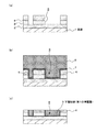
ここで、層間絶縁膜に上記MSQ(SiOC)からなる低誘電材料層を含み、Cuからなる配線およびヴィアが設けられたデュアルダマシン配線構造の製造方法の一例について、図6を用いて説明する。 Here, an example of a manufacturing method of a dual damascene wiring structure in which the interlayer dielectric film includes the low dielectric material layer made of MSQ (SiOC) and the wiring made of Cu and vias are provided will be described with reference to FIG.
まず、図6(a)に示すように、表面側に下層配線102が設けられた基板101上に、窒炭化シリコン(SiCN)からなる保護膜103を形成した後、SiOCからなる低誘電材料層104aとSiO2層104bとが順次積層された層間絶縁膜104を形成する。次に、この層間絶縁膜104に下層配線102に達する接続孔105と接続孔105の上部に連通する配線溝106を形成し、配線溝106と接続孔105の内壁を覆う状態で、層間絶縁膜104上にバリア膜107を形成する。そして、バリア膜107が設けられた配線溝106と接続孔105とを埋め込む状態で、バリア膜107上に導電膜(図示省略)を成膜し、配線パターンとして不用な導電膜およびバリア膜107をSiO2層104bが所定の膜厚となるまで除去することで、接続孔105と配線溝106とにヴィア108と上層配線109とをそれぞれ形成する。
First, as shown in FIG. 6A, a
ここで、上述したような層間絶縁膜104が低誘電材料層104aを含む配線構造では、一般的に低誘電材料層104aは膜密度が粗であることから、膜中に含まれる水分や酸素が脱ガスされ易い。このため、プロセス中、またはその後の信頼性試験等の際に、矢印Bで示すように、低誘電材料層104a自体からの脱ガス、または接続孔105および配線溝106を形成する際のエッチング乃至はレジスト剥離処理に起因する低誘電材料層104aの損傷部に付着した水分の脱ガスが生じる。これにより、低誘電材料層104aとヴィア108または上層配線109との間に介在するバリア膜107が腐食され易い。
Here, in the wiring structure in which the interlayer
そして、バリア膜107が腐蝕し、劣化すると、図6(b)に示すように、バリア膜107とCuからなるヴィア108または上層配線109との密着性が低下する。これにより、Cu原子が動きやすくなり、マイグレーションが生じるとともに、上層配線109およびヴィア108中の空孔Cが密着性の悪い部分に集合するため、バリア膜107とヴィア108または上層配線109との間にボイドVが形成され易い。このため、接続不良が生じ、配線の信頼性を著しく低下させてしまっていた。
When the
ここで、上述したデュアルダマシンの配線構造において、下層配線102の配線幅を0.7μmに固定し、上層配線109の配線幅を変化させた場合の接続不良率を測定したグラフを図7に示す。このグラフ(1)に示すように、上層配線109(前記図6(b)参照)の配線幅が広くなるほど、密着性の悪い部分に集合する空孔C(前記図6(b)参照)の量も増えるため、接続不良率が大きくなる。特に、層間絶縁膜104(前記図6(b)参照)の低誘電率化が進むと共に、上記問題は顕在化する。
Here, in the dual damascene wiring structure described above, FIG. 7 is a graph showing the connection failure rate when the wiring width of the
そこで、低誘電材料層を含む層間絶縁膜に接続孔を形成し、下層配線を露出した後、バリア膜を形成する前に、熱処理を行うことで、低誘電材料層の水分を脱ガスさせることが報告されている(例えば、特許文献1参照)。 Therefore, by forming a connection hole in the interlayer insulating film including the low dielectric material layer, exposing the lower layer wiring, and before forming the barrier film, heat treatment is performed to degas the moisture in the low dielectric material layer. Has been reported (for example, see Patent Document 1).
この層間絶縁膜の脱ガスについて、上述したデュアルダマシン配線構造の例をとり説明すると、図8に示すように、層間絶縁膜104に下層配線102に達する接続孔105と接続孔105の上部に連通する配線溝106とを形成した後、350℃程度の高温で熱処理を行う。これにより、接続孔105および配線溝106の側壁に露出された層間絶縁膜104、特に低誘電材料層104aに吸着している水分が矢印Bに示すように脱ガスされる。
The degassing of the interlayer insulating film will be described by taking the example of the dual damascene wiring structure described above. As shown in FIG. 8, the interlayer
その後、図6(a)を用いて説明したように、接続孔105と配線溝106とにバリア膜107を介してヴィア108と上層配線109とをそれぞれ形成する。これにより、図7のグラフ(2)に示すように、下層配線102(前記図6(a)参照)の配線幅を0.7μmに固定し、上層配線109(前記図6(a)参照)の配線幅を変化させた場合の接続不良率はほぼ0であり、接続不良が防止されることが判る。
Thereafter, as described with reference to FIG. 6A,
しかしながら、図8に示すように、接続孔105の底部に下層配線102を露出した状態で、350℃程度の高温で熱処理を行った場合に、上層配線109(前記図6(a)参照)の配線幅を0.7μmに固定し、下層配線102(前記図6(a)参照)の配線幅を変化させて、高温放置試験による接続不良率を測定した結果を、図9に示す。このグラフに示すように、下層配線102の配線幅が2μmを超えると高温放置試験により接続不良が発生することが確認された。この接続不良率は下層配線102の配線幅に依存しており、配線幅が広くなるに従い、接続不良率の上昇が確認された。そして、この不良箇所を解析した結果、ボイドが確認された。
However, as shown in FIG. 8, when heat treatment is performed at a high temperature of about 350 ° C. with the
このボイドの発生メカニズムは、以下のように推定され、Thermally Robust Cu Interconnects with Cu-Ag Alloy fir sub 45nm Node「International Electron Devices Meeting」(米)IEEE,2004年で報告されている。すなわち、図10(a)に示すように、接続孔105の底部に下層配線102を露出した状態で、350℃程度の高温の熱処理を行うと、下層配線102が接続孔105の底部で隆起する様な変形が生じる。
The generation mechanism of this void is estimated as follows, and reported in Thermally Robust Cu Interconnects with Cu-Ag Alloy fir sub 45 nm Node “International Electron Devices Meeting” (USA) IEEE, 2004. That is, as shown in FIG. 10A, when heat treatment at a high temperature of about 350 ° C. is performed with the
この変形は、下層配線102を構成する導電材料の軟化温度以上の温度を加えた時に、再結晶化等により、応力緩和する為に発生すると考えられる。また、この下層配線102の隆起は、下層配線102の体積(配線幅×配線長×膜厚)と、その下層配線102への接続孔105の数に依存し、接続孔105の数が少なく、且つ下層配線102の体積が大きい程、大きく隆起する。
This deformation is considered to occur to relieve stress due to recrystallization or the like when a temperature equal to or higher than the softening temperature of the conductive material constituting the
そして、図10(b)に示すように、接続孔105の底部に下層配線102が隆起した状態で、配線溝106および接続孔105の内壁にバリア膜107が形成される為、最終工程まで経た半導体装置は、接続孔105の底部に隆起した下層配線102上に、ヴィア108を介して上層配線109が形成された構造となる。
Then, as shown in FIG. 10B, the
その後、この接続孔105の底部の隆起箇所には応力勾配が残留する為、バリア膜107と下層配線102との密着性が低下することで、Cu元素が動きやすくなり、マイグレーションが生じるとともに、下層配線102中の空孔C’が密着性の悪い箇所に集合して、ボイドV’が形成される。
Thereafter, since a stress gradient remains in the raised portion at the bottom of the
かかる問題点を改善するため、本発明は、接続孔または配線溝の側壁に露出される層間絶縁膜に吸着している水分を確実に脱ガスさせて除去するとともに、接続孔の底部への下層配線の隆起を防ぐことが可能な半導体装置の製造方法を提供することを目的とする。 In order to improve such a problem, the present invention reliably removes the moisture adsorbed on the interlayer insulating film exposed on the side wall of the connection hole or wiring groove by removing the gas reliably, and lowering the bottom of the connection hole. An object of the present invention is to provide a method of manufacturing a semiconductor device capable of preventing the wiring from being raised.
上記目的を達成するために、本発明の半導体装置の製造方法は、次のような工程を順次行うことを特徴としている。まず、表面側に第1の導電層が設けられた基板上に、保護膜と絶縁膜とを順次形成する工程を行う。次に、第1の導電層上の絶縁膜に、保護膜に達する凹部を形成する工程を行う。次いで、凹部の底部に保護膜を残存させた状態で、第1の熱処理を行う。続いて、保護膜を除去し、凹部の底部に第1の導電層を露出させる工程を行う。次に、凹部の底部に第1の導電層を露出させた状態で、第1の熱処理よりも低い温度で第2の熱処理を行う。その後、凹部を第2の導電層で埋め込む工程を行う。 In order to achieve the above object, a method of manufacturing a semiconductor device according to the present invention is characterized by sequentially performing the following steps. First, a step of sequentially forming a protective film and an insulating film on a substrate provided with a first conductive layer on the surface side is performed. Next, a step of forming a recess reaching the protective film in the insulating film on the first conductive layer is performed. Next, a first heat treatment is performed with the protective film remaining at the bottom of the recess. Then, the process of removing a protective film and exposing a 1st conductive layer to the bottom part of a recessed part is performed. Next, a second heat treatment is performed at a lower temperature than the first heat treatment with the first conductive layer exposed at the bottom of the recess. Thereafter, a step of filling the concave portion with the second conductive layer is performed.
このような半導体装置の製造方法によれば、凹部の底部に保護膜を残存させた状態で第1の熱処理を行うことから、凹部の側壁に露出される絶縁膜に吸着している水分を確実に除去する温度で第1の熱処理を行ったとしても、凹部の底部に第1の導電層が隆起することが防止される。その後、凹部の底部に第1の導電層を露出させた状態で、第1の熱処理よりも低い温度で第2の熱処理を行うことで、凹部の側壁に露出される絶縁膜に第1の熱処理後に吸着した水分が、凹部を第2の導電層で埋め込む前に除去される。 According to such a method of manufacturing a semiconductor device, since the first heat treatment is performed with the protective film remaining on the bottom of the recess, the moisture adsorbed on the insulating film exposed on the side wall of the recess is reliably ensured. Even if the first heat treatment is performed at a temperature at which the first conductive layer is removed, the first conductive layer is prevented from rising at the bottom of the recess. Thereafter, the second heat treatment is performed at a temperature lower than the first heat treatment with the first conductive layer exposed at the bottom of the recess, whereby the first heat treatment is performed on the insulating film exposed on the sidewall of the recess. Moisture adsorbed later is removed before the recess is filled with the second conductive layer.
以上、説明したように、本発明の半導体装置の製造方法によれば、凹部を第2の導電層で埋め込む前に凹部の側壁に露出される絶縁膜に吸着している水分が確実に除去されるため、絶縁膜に吸着した水分がプロセス中またはその後の高温放置試験中に脱ガスされることが防止される。これにより、脱ガスに起因して第2の導電層中にボイドが発生することが防止される。また、凹部の底部に第1の導電層が隆起することが防止されるため、凹部の底部に第1の導電層の隆起に起因するボイドが発生することが防止される。以上のことから、前記凹部が配線溝または接続孔である場合には、上記ボイドによる接続不良が抑制され、配線信頼性を向上させることができる。 As described above, according to the method for manufacturing a semiconductor device of the present invention, moisture adsorbed on the insulating film exposed on the side wall of the recess is reliably removed before the recess is embedded with the second conductive layer. Therefore, it is possible to prevent the moisture adsorbed on the insulating film from being degassed during the process or the subsequent high temperature standing test. This prevents voids from being generated in the second conductive layer due to degassing. In addition, since the first conductive layer is prevented from rising at the bottom of the recess, it is possible to prevent the occurrence of voids due to the protrusion of the first conductive layer at the bottom of the recess. From the above, when the concave portion is a wiring groove or a connection hole, connection failure due to the void is suppressed, and wiring reliability can be improved.
以下、本発明の実施の形態を図面に基づいて詳細に説明する。 Hereinafter, embodiments of the present invention will be described in detail with reference to the drawings.
本実施形態例は、本発明にかかる半導体装置の製造方法の実施形態の一例であり、デュアルダマシン構造の形成に係わる。以下、図1〜図3および図5の製造工程断面図を用いて本発明の第1実施形態を説明する。 The present embodiment is an example of an embodiment of a method for manufacturing a semiconductor device according to the present invention, and relates to the formation of a dual damascene structure. Hereinafter, the first embodiment of the present invention will be described with reference to the manufacturing process cross-sectional views of FIGS. 1 to 3 and FIG. 5.
まず、図1(a)に示すように、素子領域等(図示省略)が形成された下地となるシリコン基板(基板)1上に、下地絶縁膜2を介して膜厚100nmのPAE膜3と膜厚100nmのSiO2膜4(比誘電率4.1)とからなる積層膜を配線間絶縁膜として成膜する。次いで、通常のリソグラフィー技術およびエッチング技術により、この配線間絶縁膜に200nmの深さの配線溝5を形成する。なお、ここでの図示は省略するが、この段階で、下地絶縁膜2にも基板11に達する接続孔が既に形成されている。
First, as shown in FIG. 1A, a
次に、図1(b)に示すように、スパッタリング法により、配線溝5の内壁を覆う状態で、SiO2膜4上に、タンタル(Ta)からなるバリア膜6を10nmの膜厚で形成する。続いて、スパッタリング法により、バリア膜6上に、銅(Cu)からなるシード層7を80nmの膜厚で成膜する。その後、電解めっき法により、配線溝5を埋め込む状態で、シード層7上に、Cuめっき層8を700nmの膜厚で形成する。 Next, as shown in FIG. 1B, a barrier film 6 made of tantalum (Ta) is formed to a thickness of 10 nm on the SiO 2 film 4 so as to cover the inner wall of the wiring groove 5 by sputtering. To do. Subsequently, a seed layer 7 made of copper (Cu) is formed to a thickness of 80 nm on the barrier film 6 by a sputtering method. Thereafter, a Cu plating layer 8 having a thickness of 700 nm is formed on the seed layer 7 in a state where the wiring groove 5 is embedded by an electrolytic plating method.
次いで、図1(c)に示すように、熱処理によりCuの結晶成長を行い、化学的機械的研磨(Chemical Mechanical Polishing(CMP))法により、Cuめっき層8(前記図1(b)参照)、シード層7(前記図1(b)参照)およびバリア膜6をSiO2膜4が所定の膜厚となるまで研磨し、Cuからなる下層配線9を形成する。なお、SiO2膜4は、埋め込み配線形成過程でCMP法により90nm研磨される。ここまでの構成が請求項1の基板に相当する。
Next, as shown in FIG. 1C, Cu crystal growth is performed by heat treatment, and a Cu plating layer 8 (see FIG. 1B) is formed by a chemical mechanical polishing (CMP) method. Then, the seed layer 7 (see FIG. 1B) and the barrier film 6 are polished until the SiO 2 film 4 has a predetermined thickness to form a lower layer wiring 9 made of Cu. The SiO 2 film 4 is polished by 90 nm by the CMP method in the process of forming the embedded wiring. The configuration so far corresponds to the substrate of
その後、図2(d)に示すように、下層配線9上およびSiO2膜4上に、例えばSiCからなる保護膜10を35nmの膜厚で形成する。この保護膜10は、後工程で、この保護膜10の上層に形成する第1絶縁膜をエッチングして接続孔を形成する際に、下層配線9の露出およびSiO2膜4への掘り込みを防止するエッチングストッパー膜であるとともに、下層配線9の拡散防止膜および酸化防止膜としても機能する。なお、ここでは、保護膜10にSiCを用いることとしたが、SiCNであってもよい。
Thereafter, as shown in FIG. 2D, a
次に、この保護膜10上に、配線層間絶縁膜として、低誘電材料からなる第1絶縁膜11を形成する。ここでは、例えば無機系の低誘電材料である、比誘電率2.3のMSQ、すなわち炭素含有酸化シリコン(SiOC)からなる第1絶縁膜11を150nmの膜厚で形成することとする。なお、ここでは、第1絶縁膜11としてMSQを用いることとしたが、HSQであってもよい。
Next, a first insulating
次いで、第1絶縁膜11上に、第1絶縁膜11とは異なる低誘電率材料からなる第2絶縁膜12を形成する。ここでは、第2絶縁膜12に、有機系の低誘電材料として、特に有機ポリマー材料を用いることとし、一例として、比誘電率2.3のポリアリールエーテル(PAE)からなる第2絶縁膜12を100nmの膜厚で形成する。なお、ここでは、第2絶縁膜12として、PAEを用いることとしたが、ベンゾシクロブテン(BCB)、或いは、フロロカーボン(CFx)であってもよい。
Next, a second insulating
次に、第2絶縁膜12上に、例えばSiO2からなる第1マスク形成層13を140nmの膜厚で成膜する。この第1マスク形成層13の上層部分は、後工程で行うCMPの削りしろとなる。
Next, a first
次いで、例えばSiNからなる第2マスク形成層14を50nmの膜厚で形成した後、例えばSiO2からなる第3マスク形成層15を50nmの膜厚で形成する。
Next, the second
続いて、第3マスク形成層15上に、配線溝パターンを有するレジストマスク(図示省略)を形成する。
Subsequently, a resist mask (not shown) having a wiring groove pattern is formed on the third
次に、図2(e)に示すように、レジストマスクをエッチングマスクとして用いたドライエッチング法により、第3マスク形成層(SiO2)15(前記図2(d)参照)をエッチングして、配線溝パターンを有する第3マスク(SiO2)15’を形成する。その後、アッシング処理と薬液処理を施すことにより、上記レジストマスクおよびエッチング処理の際に生じた残留付着物を完全に除去する。 Next, as shown in FIG. 2E, the third mask formation layer (SiO 2 ) 15 (see FIG. 2D) is etched by a dry etching method using the resist mask as an etching mask. A third mask (SiO 2 ) 15 ′ having a wiring groove pattern is formed. Thereafter, by performing ashing treatment and chemical treatment, the resist mask and the residual deposits produced during the etching treatment are completely removed.
次に、図2(f)に示すように、第3マスク15’上を含む第2マスク形成層14上に、接続孔パターンを有するレジストマスクRを形成する。この際、レジストマスクRに設けられた接続孔パターンの少なくとも一部が、第3マスク15’の開口部内に重なるように、レジストマスクRをパターン形成する。
Next, as shown in FIG. 2F, a resist mask R having a connection hole pattern is formed on the second
続いて、図3(g)に示すように、レジストマスクR(前記図2(f)参照)をエッチングマスクとしたドライエッチング法により、第3マスク15’、第2マスク形成層14、第1マスク形成層13をエッチングし、さらに第2絶縁膜12をエッチングする。これにより、第1絶縁膜11の表面に到達する接続孔16を開口する。この際、レジストマスクRと第2絶縁膜12のエッチングレートはほぼ同等であることから、第2絶縁膜12のエッチング中にレジストマスクRは膜減りし、除去される。
Subsequently, as shown in FIG. 3G, the
次に、図3(h)に示すように、配線溝パターンを有する第3マスク(SiO2)15’をエッチングマスクとしたドライエッチング法により、第2マスク形成層(SiN)14(前記図3(g)参照)をエッチングする。これにより、配線溝パターンを有する第2マスク14’が形成される。また、このエッチングの際、接続孔16の底部に露出するSiOCからなる第1絶縁膜11は、途中まで掘り下げられる。
Next, as shown in FIG. 3H, the second mask formation layer (SiN) 14 (see FIG. 3) is formed by a dry etching method using the third mask (SiO 2 ) 15 ′ having the wiring groove pattern as an etching mask. (G) is etched. As a result, a
次に、図3(i)に示すように、第3マスク(SiO2)15’(前記図3(h)参照)および第2マスク(SiN)14’をエッチングマスクとして用いたドライエッチングにより、第1マスク形成層(SiO2)13(前記図3(h)参照)をエッチングする。これにより、配線溝パターン有する第1マスク13’が形成される。
Next, as shown in FIG. 3I, by dry etching using the third mask (SiO 2 ) 15 ′ (see FIG. 3H) and the second mask (SiN) 14 ′ as an etching mask, The first mask formation layer (SiO 2 ) 13 (see FIG. 3H) is etched. As a result, a
この際、第3マスク(SiO2)15’は、第1マスク形成層(SiO2)13と同一材料であるため、第1マスク形成層13のエッチングの進行にともない、第3マスク15’も除去される。また、このエッチングにより、第1絶縁膜11の途中まで掘り下げられた接続孔16は更に掘り下げられ、保護膜(SiC)10に達する。
At this time, since the third mask (SiO 2 ) 15 ′ is made of the same material as the first mask formation layer (SiO 2 ) 13, the
ここで、接続孔16の底部に保護膜10が残存した状態で、接続孔15の側壁に露出される第1絶縁膜11および第2絶縁膜12に吸着している水分を除去するため、第1の熱処理を行う。ここで、第1絶縁膜11および第2絶縁膜12に吸着している水分には、物理吸着している水分と化学吸着している水分とがある。化学吸着している水分とは、物理吸着している水分が上記絶縁膜中に取り込まれ、水素結合を形成したものを指す。物理吸着している水分が絶縁膜中に拡散され、化学吸着するにはある程度の時間を要すると考えられる。
Here, in order to remove moisture adsorbed on the first insulating
ここで、図4に本実施形態で配線層間絶縁膜として用いたSiOCからなる低誘電材料層の昇温脱離分析(TDS)の結果を示すと、350℃程度でピークを示しており、350℃程度で熱処理を行うことで、低誘電材料層に化学吸着している水分が除去されることが判る。また、低誘電材料層に物理吸着している水分は、化学吸着している水分よりも低い温度で除去される。 Here, FIG. 4 shows a temperature desorption analysis (TDS) result of the low dielectric material layer made of SiOC used as the wiring interlayer insulating film in this embodiment, and shows a peak at about 350 ° C. It can be seen that the moisture chemically adsorbed on the low dielectric material layer is removed by performing the heat treatment at about ° C. Further, the moisture physically adsorbed on the low dielectric material layer is removed at a temperature lower than the moisture that is chemically adsorbed.
この第1の熱処理は、図3(i)に示す低誘電材料からなる第1絶縁膜11および第2絶縁膜12に化学的に吸着している水分が除去される程度の温度および時間で行うこととする。具体的には300℃〜400℃の温度で1分〜60分間行い、ここでは、350℃で10分間の熱処理を行うこととする。これにより、矢印Aに示すように、接続孔16の側壁に露出される第1絶縁膜11および第2絶縁膜12に化学吸着している水分と物理吸着している水分とが脱ガスされ、確実に除去される。また、この際、下層配線9上は保護膜10で覆われていることから、接続孔16の底部からの下層配線9の隆起は防止される。
The first heat treatment is performed at a temperature and a time at which the moisture chemically adsorbed on the first insulating
続いて、図5(j)に示すように、接続孔16の底部の保護膜10をエッチング除去し、下層配線9を露出させるとともに、第2マスク14’(前記図3(i)参照)をエッチング除去する。
Subsequently, as shown in FIG. 5 (j), the
次いで、第1マスク(SiO2)13’をエッチングマスクとして、第1マスク13’の配線溝パターンの底部に残存する第2絶縁膜(PAE)12をエッチングする。これにより、第1マスク13’に形成された配線溝パターンを掘り下げて、第1マスク13’と第2絶縁膜12とに配線溝17が形成された状態となる。これにより、配線溝17が接続孔16を介して下層配線9と連通した状態となる。
Next, the second insulating film (PAE) 12 remaining at the bottom of the wiring groove pattern of the
なお、本実施形態では、保護膜10および第2マスク14’を除去後、第2絶縁膜12の配線溝加工を行ったが、第2絶縁膜12の配線溝加工後、保護膜10および第2マスク14’を除去することも可能である。
In this embodiment, after removing the
その後、薬液を用いた後処理を行い、配線溝17や接続孔16の側壁に残留するエッチング付着物を除去した後、第2の熱処理を行う。この第2の熱処理では、図3(i)を用いて説明した第1の熱処理後の各工程中で、配線溝17および接続孔16の側壁に吸着した水分を除去する。ここで、上述したように、絶縁膜の表面に物理吸着している水分が絶縁膜中に拡散され水素結合を形成するまでには、ある程度の時間を要するため、第1の熱処理後に配線溝17や接続孔16の側壁に吸着した水分は物理吸着していると考えられる。
Thereafter, a post-treatment using a chemical solution is performed to remove etching deposits remaining on the side walls of the
このため、第2の熱処理は第1の熱処理よりも低い温度で行い、図4を用いて説明したように、100℃〜300℃の範囲で1分〜30分間行うこととする。この際、下層配線9は、接続孔16の底部に露出されていることから、接続孔16底部からの下層配線9の隆起を防ぐために、下層配線9を構成するCuの軟化温度よりも同程度以下の温度で行うことが好ましい。ただし、第1絶縁膜11および第2絶縁膜12に物理吸着している水分を確実に除去するためには、上記範囲内で第2の熱処理の温度は高い方が好ましいことから、ここでは、下層配線9を構成するCuの軟化温度と同程度の250℃で2分間、第2の熱処理を行うこととする。これにより、配線溝17や接続孔16の側壁に露出された第1絶縁膜11および第2絶縁膜12に吸着している水分は、矢印A’に示すように脱ガスされる。
Therefore, the second heat treatment is performed at a temperature lower than that of the first heat treatment, and is performed in the range of 100 ° C. to 300 ° C. for 1 minute to 30 minutes as described with reference to FIG. At this time, since the lower layer wiring 9 is exposed at the bottom of the
なお、ここでは250℃の熱をかけて熱処理を行うこととしたが、配線溝17や接続孔16の側壁に残留するエッチング付着物を除去するとともに接続孔底部のCu変質層を正常なCu層に転化するRFスパッタリング処理によっても、基板の温度は上昇するため、上記スパッタリング処理も第2の熱処理に含まれることとする。
Here, the heat treatment is performed by applying heat at 250 ° C., but the etching deposits remaining on the side walls of the
上記第2の熱処理を行った後、図5(k)に示すように、例えばスパッタリング法により、上記配線溝17および接続孔16の内壁を覆う状態で、例えばTaからなるバリア膜18を成膜する。ここで、上記配線溝17および接続孔16の側壁に露出される第1絶縁膜11および第2絶縁膜12への水分の吸着を防ぐため、第2の熱処理後からバリア膜18を形成するまでは、大気に接触させないことが好ましい。
After performing the second heat treatment, as shown in FIG. 5 (k), a barrier film 18 made of Ta, for example, is formed by sputtering, for example, so as to cover the inner walls of the
続いて、上記配線溝17および接続孔16を埋め込む状態で、バリア膜18上にCuAgからなるシード層19を形成する。その後、例えば電解めっき法により、Cuからなるメッキ層20を堆積し、配線溝17と接続孔16の埋め込みを同時に行う。
Subsequently, a
次に、図5(l)に示すように、CMP法により、配線パターンとして不要なメッキ層20(シード層19も含む)(前記図5(k)参照)、バリア膜18を、第1マスク13’が所定の膜厚となるまで除去することで、接続孔16にヴィア21(第2の導電層)を形成するとともに配線溝17に上層配線22(第2の導電層)を形成する。この後の工程は、図2(d)〜図5(l)を用いて説明した工程を繰り返して行うことにより、多層配線構造を完成させる。
Next, as shown in FIG. 5L, the plating layer 20 (including the seed layer 19) unnecessary as a wiring pattern (see FIG. 5K) and the barrier film 18 are formed on the first mask by CMP. By removing 13 ′ until the film thickness reaches a predetermined thickness, a via 21 (second conductive layer) is formed in the
このような半導体装置の製造方法によれば、接続孔16の底部に保護膜10が残存した状態で第1の熱処理を行うことから、接続孔16の側壁に露出される第1絶縁膜11および第2絶縁膜12に化学吸着している水分を脱ガスさせる温度で第1の熱処理を行ったとしても、接続孔16の底部に下層配線9が隆起することが防止される。その後、接続孔15の底部に下層配線9を露出した状態で、第1の熱処理よりも低い温度で第2の熱処理を行うことで、接続孔16および配線溝17の側壁に露出される第1絶縁膜11および第2絶縁膜12に第1の熱処理後に物理吸着した水分が、バリア膜18の形成前に除去される。
According to such a method of manufacturing a semiconductor device, since the first heat treatment is performed with the
したがって、プロセス中またはその後の高温放置試験中に第1絶縁膜11および第2絶縁膜12に吸着している水分が脱ガスされることによるバリア膜18の劣化が防止され、バリア膜18とヴィア21および上層配線22との密着性が低下することによるボイドの発生が抑制される。また、接続孔15の底部に下層配線9が隆起することが防止されるため、接続孔15の底部にボイドが発生することが抑制される。以上のことから、ボイドに起因する接続不良が抑制され、配線信頼性を向上させることができる。
Therefore, deterioration of the barrier film 18 due to degassing of moisture adsorbed on the first insulating
なお、本実施形態では、下層配線9の材料として、Cuを用いることとするが、配線およびヴィアの構成材料については特に限定されるものではない。特に、配線およびヴィアの構成材料に銅銀(CuAg)合金の如き軟化温度の高い材料を使用すると、接続孔16の底部に下層配線9を露出した状態で行う第2の熱処理の際、Cuを用いた場合よりも高い温度をかけることができ、第2の熱処理の温度に裕度を持たせることができるため、好ましい。この場合には、図1(b)を用いて説明した工程において、配線溝5の内壁を覆う状態でバリア膜6を形成した後、バリア膜6上にCuAgからなるシード層7を形成し、配線溝5を埋め込む状態でシード層7上にCuめっき層8を形成する。続いて、熱処理を行うことによりシード層7の銀(Ag)をCuめっき層8に拡散させる。その後は図1(c)を用いて説明した工程を行う。
In the present embodiment, Cu is used as the material of the lower layer wiring 9, but the constituent materials of the wiring and vias are not particularly limited. In particular, when a material having a high softening temperature such as a copper-silver (CuAg) alloy is used for the constituent material of the wiring and via, Cu is used in the second heat treatment performed with the lower layer wiring 9 exposed at the bottom of the
また、上記実施形態では、デュアルダマシン配線構造の製造方法を例にとり説明したが、シングルダマシン配線構造であっても適用可能である。この場合には、表面側に下層配線が設けられた基板上に保護膜および絶縁膜を順次形成した後、絶縁膜に保護膜を露出する接続孔を形成し、第1の熱処理を行う。次いで、接続孔の底部に露出した保護膜を除去して、導電層を露出した後、第1の熱処理よりも低い温度で第2の熱処理を行った後、接続孔にヴィアを形成する。ただし、デュアルダマシン配線構造の製造方法に本発明を適用する方が、配線溝17と接続孔16の側壁に露出される層間絶縁膜14の面積が広くなるため、顕著な効果を奏する。
In the above embodiment, the method for manufacturing a dual damascene wiring structure has been described as an example. However, the present invention is also applicable to a single damascene wiring structure. In this case, after a protective film and an insulating film are sequentially formed on a substrate having a lower layer wiring on the front side, a connection hole exposing the protective film is formed in the insulating film, and a first heat treatment is performed. Next, after removing the protective film exposed at the bottom of the connection hole to expose the conductive layer, a second heat treatment is performed at a temperature lower than the first heat treatment, and then a via is formed in the connection hole. However, applying the present invention to the manufacturing method of the dual damascene wiring structure has a remarkable effect because the area of the
1…基板、9…下層配線(第1の導電層)、10…保護膜、11…第1絶縁膜(低誘電材料層)、12…第2絶縁膜(低誘電材料層)、16…接続孔、17…配線溝、21…ヴィア(第2の導電層)、22…上層配線(第2の導電層)
DESCRIPTION OF
Claims (4)
前記第1の導電層上の前記絶縁膜に、前記保護膜に達する凹部を形成する工程と、
前記凹部の底部に前記保護膜を残存させた状態で、第1の熱処理を行う工程と、
前記第1の熱処理後に、前記保護膜を除去し、前記凹部の底部に前記第1の導電層を露出させる工程と、
前記凹部の底部に前記第1の導電層を露出させた状態で、前記第1の熱処理よりも低い温度で第2の熱処理を行う工程と、
前記第2の熱処理後に、前記凹部を第2の導電層で埋め込む工程とを有する
ことを特徴とする半導体装置の製造方法。 A step of sequentially forming a protective film and an insulating film on a substrate provided with a first conductive layer on the surface side;
Forming a recess reaching the protective film in the insulating film on the first conductive layer;
Performing a first heat treatment with the protective film remaining at the bottom of the recess;
Removing the protective film after the first heat treatment and exposing the first conductive layer to the bottom of the recess;
Performing a second heat treatment at a temperature lower than the first heat treatment with the first conductive layer exposed at the bottom of the recess;
Filling the recess with a second conductive layer after the second heat treatment. A method for manufacturing a semiconductor device, comprising:
前記第2の熱処理は、前記凹部の側壁に露出される前記絶縁膜に物理吸着している水分が除去される温度で行う
ことを特徴とする請求項1記載の半導体装置の製造方法。 The first heat treatment is performed at a temperature at which moisture chemically adsorbed on the insulating film exposed on the side wall of the recess is removed.
2. The method of manufacturing a semiconductor device according to claim 1, wherein the second heat treatment is performed at a temperature at which moisture physically adsorbed on the insulating film exposed on the side wall of the recess is removed.
ことを特徴とする請求項1記載の半導体装置の製造方法。 The method for manufacturing a semiconductor device according to claim 1, wherein the insulating film includes a low dielectric material layer made of a material having a dielectric constant lower than that of silicon oxide.
前記凹部の内壁を覆う状態で、前記第2の導電層から前記絶縁膜への導電材料の拡散を防止するバリア膜を形成する工程を行う
ことを特徴とする請求項1記載の半導体装置の製造方法。
After the step of performing the second heat treatment, before the step of filling the concave portion with the second conductive layer,
The manufacturing method of a semiconductor device according to claim 1, wherein a step of forming a barrier film for preventing diffusion of a conductive material from the second conductive layer to the insulating film is performed in a state of covering the inner wall of the recess. Method.
Priority Applications (1)
| Application Number | Priority Date | Filing Date | Title |
|---|---|---|---|
| JP2005254683A JP4525534B2 (en) | 2005-09-02 | 2005-09-02 | Manufacturing method of semiconductor device |
Applications Claiming Priority (1)
| Application Number | Priority Date | Filing Date | Title |
|---|---|---|---|
| JP2005254683A JP4525534B2 (en) | 2005-09-02 | 2005-09-02 | Manufacturing method of semiconductor device |
Publications (2)
| Publication Number | Publication Date |
|---|---|
| JP2007067324A true JP2007067324A (en) | 2007-03-15 |
| JP4525534B2 JP4525534B2 (en) | 2010-08-18 |
Family
ID=37929136
Family Applications (1)
| Application Number | Title | Priority Date | Filing Date |
|---|---|---|---|
| JP2005254683A Expired - Fee Related JP4525534B2 (en) | 2005-09-02 | 2005-09-02 | Manufacturing method of semiconductor device |
Country Status (1)
| Country | Link |
|---|---|
| JP (1) | JP4525534B2 (en) |
Cited By (3)
| Publication number | Priority date | Publication date | Assignee | Title |
|---|---|---|---|---|
| KR20170012132A (en) | 2015-07-24 | 2017-02-02 | 가부시키가이샤 히다치 고쿠사이 덴키 | Method of manufacturing semiconductor device, substrate processing apparatus, and program |
| KR20170018343A (en) | 2014-06-25 | 2017-02-17 | 가부시키가이샤 히다치 고쿠사이 덴키 | Substrate-processing device, program, and method for manufacturing semiconductor device |
| CN108231659A (en) * | 2016-12-15 | 2018-06-29 | 中芯国际集成电路制造(北京)有限公司 | Interconnection structure and its manufacturing method |
Citations (7)
| Publication number | Priority date | Publication date | Assignee | Title |
|---|---|---|---|---|
| JPH0547759A (en) * | 1991-08-19 | 1993-02-26 | Matsushita Electron Corp | Manufacture of semiconductor device |
| JPH10144685A (en) * | 1996-11-13 | 1998-05-29 | Sony Corp | Wiring structure of semiconductor device and method for forming the same |
| JPH10233444A (en) * | 1997-02-19 | 1998-09-02 | Mitsubishi Electric Corp | Manufacture of semiconductor device |
| JP2000150646A (en) * | 1998-11-11 | 2000-05-30 | Sony Corp | Semiconductor device and its manufacture |
| JP2004140263A (en) * | 2002-10-18 | 2004-05-13 | Fujitsu Ltd | Substrate processing method and wiring structure forming method |
| JP2004253671A (en) * | 2003-02-21 | 2004-09-09 | Renesas Technology Corp | Manufacturing method of electron device |
| JP2004356500A (en) * | 2003-05-30 | 2004-12-16 | Renesas Technology Corp | Method for manufacturing electronic device |
-
2005
- 2005-09-02 JP JP2005254683A patent/JP4525534B2/en not_active Expired - Fee Related
Patent Citations (7)
| Publication number | Priority date | Publication date | Assignee | Title |
|---|---|---|---|---|
| JPH0547759A (en) * | 1991-08-19 | 1993-02-26 | Matsushita Electron Corp | Manufacture of semiconductor device |
| JPH10144685A (en) * | 1996-11-13 | 1998-05-29 | Sony Corp | Wiring structure of semiconductor device and method for forming the same |
| JPH10233444A (en) * | 1997-02-19 | 1998-09-02 | Mitsubishi Electric Corp | Manufacture of semiconductor device |
| JP2000150646A (en) * | 1998-11-11 | 2000-05-30 | Sony Corp | Semiconductor device and its manufacture |
| JP2004140263A (en) * | 2002-10-18 | 2004-05-13 | Fujitsu Ltd | Substrate processing method and wiring structure forming method |
| JP2004253671A (en) * | 2003-02-21 | 2004-09-09 | Renesas Technology Corp | Manufacturing method of electron device |
| JP2004356500A (en) * | 2003-05-30 | 2004-12-16 | Renesas Technology Corp | Method for manufacturing electronic device |
Cited By (11)
| Publication number | Priority date | Publication date | Assignee | Title |
|---|---|---|---|---|
| KR20170018343A (en) | 2014-06-25 | 2017-02-17 | 가부시키가이샤 히다치 고쿠사이 덴키 | Substrate-processing device, program, and method for manufacturing semiconductor device |
| US20170103885A1 (en) | 2014-06-25 | 2017-04-13 | Hitachi Kokusai Electric Inc. | Method for manufacturing semiconductor device, substrate-processing apparatus, and recording medium |
| US10163625B2 (en) | 2014-06-25 | 2018-12-25 | Hitachi Kokusai Electric Inc. | Method for manufacturing semiconductor device, substrate-processing apparatus, and recording medium |
| US10229829B2 (en) | 2014-06-25 | 2019-03-12 | Kokusai Electric Corporation | Method for manufacturing semiconductor device, substrate-processing apparatus, and recording medium |
| US10497561B2 (en) | 2014-06-25 | 2019-12-03 | Kokusai Electric Corporation | Method for manufacturing semiconductor device, substrate-processing apparatus, and recording medium |
| KR20170012132A (en) | 2015-07-24 | 2017-02-02 | 가부시키가이샤 히다치 고쿠사이 덴키 | Method of manufacturing semiconductor device, substrate processing apparatus, and program |
| CN108231659A (en) * | 2016-12-15 | 2018-06-29 | 中芯国际集成电路制造(北京)有限公司 | Interconnection structure and its manufacturing method |
| EP3336895A3 (en) * | 2016-12-15 | 2018-07-04 | Semiconductor Manufacturing International Corporation (Beijing) | Method for fabricating damascene structure using fluorocarbon film |
| US10504883B2 (en) | 2016-12-15 | 2019-12-10 | Semiconductor Manufacturing International (Beijing) Corporation | Method for fabricating damascene structure using fluorocarbon film |
| CN108231659B (en) * | 2016-12-15 | 2020-07-07 | 中芯国际集成电路制造(北京)有限公司 | Interconnect structure and method of making the same |
| US11081478B2 (en) | 2016-12-15 | 2021-08-03 | Semiconductor Manufacturing International (Beijing) Corporation | Interconnect structure having a fluorocarbon layer |
Also Published As
| Publication number | Publication date |
|---|---|
| JP4525534B2 (en) | 2010-08-18 |
Similar Documents
| Publication | Publication Date | Title |
|---|---|---|
| US7871923B2 (en) | Self-aligned air-gap in interconnect structures | |
| JP4918778B2 (en) | Manufacturing method of semiconductor integrated circuit device | |
| US8748314B2 (en) | Method of manufacturing a semiconductor device | |
| JP2005072384A (en) | Method for manufacturing electronic device | |
| JP2006253504A (en) | Semiconductor device and its manufacturing method | |
| KR20060065512A (en) | Manufacturing Method of Semiconductor Device and Semiconductor Device | |
| US20090081865A1 (en) | Method for fabricating semiconductor device | |
| JP4419025B2 (en) | Manufacturing method of semiconductor device | |
| JP2007294625A (en) | Manufacturing method of semiconductor device | |
| JP4525534B2 (en) | Manufacturing method of semiconductor device | |
| JP5200436B2 (en) | Manufacturing method of semiconductor device | |
| JP4219215B2 (en) | Manufacturing method of electronic device | |
| JP4160489B2 (en) | Manufacturing method of semiconductor device | |
| JP4383262B2 (en) | Semiconductor device and manufacturing method thereof | |
| KR100691105B1 (en) | Copper wiring formation method using dual damascene process | |
| JP4797821B2 (en) | Manufacturing method of semiconductor device | |
| JP2008041783A (en) | Manufacturing method of semiconductor device | |
| KR100914976B1 (en) | Method of manufacturing semiconductor device | |
| JP2007214418A (en) | Semiconductor device manufacturing method | |
| JP2004296620A (en) | Process for fabricating semiconductor device | |
| JP4695842B2 (en) | Semiconductor device and manufacturing method thereof | |
| KR100678003B1 (en) | How to form a dual damascene pattern | |
| JP2005217223A (en) | Method for manufacturing semiconductor device | |
| JP2006140373A (en) | Manufacturing method for semiconductor device | |
| JP2000114375A (en) | Manufacture of semiconductor device |
Legal Events
| Date | Code | Title | Description |
|---|---|---|---|
| A621 | Written request for application examination |
Free format text: JAPANESE INTERMEDIATE CODE: A621 Effective date: 20080723 |
|
| RD02 | Notification of acceptance of power of attorney |
Free format text: JAPANESE INTERMEDIATE CODE: A7422 Effective date: 20091009 |
|
| RD04 | Notification of resignation of power of attorney |
Free format text: JAPANESE INTERMEDIATE CODE: A7424 Effective date: 20091105 |
|
| A977 | Report on retrieval |
Free format text: JAPANESE INTERMEDIATE CODE: A971007 Effective date: 20100219 |
|
| A131 | Notification of reasons for refusal |
Free format text: JAPANESE INTERMEDIATE CODE: A131 Effective date: 20100302 |
|
| A521 | Written amendment |
Free format text: JAPANESE INTERMEDIATE CODE: A523 Effective date: 20100412 |
|
| TRDD | Decision of grant or rejection written | ||
| A01 | Written decision to grant a patent or to grant a registration (utility model) |
Free format text: JAPANESE INTERMEDIATE CODE: A01 Effective date: 20100511 |
|
| A01 | Written decision to grant a patent or to grant a registration (utility model) |
Free format text: JAPANESE INTERMEDIATE CODE: A01 |
|
| A61 | First payment of annual fees (during grant procedure) |
Free format text: JAPANESE INTERMEDIATE CODE: A61 Effective date: 20100524 |
|
| FPAY | Renewal fee payment (event date is renewal date of database) |
Free format text: PAYMENT UNTIL: 20130611 Year of fee payment: 3 |
|
| FPAY | Renewal fee payment (event date is renewal date of database) |
Free format text: PAYMENT UNTIL: 20130611 Year of fee payment: 3 |
|
| LAPS | Cancellation because of no payment of annual fees |