JP2006074524A - Serial signal transmitting device, serial signal receiving device, serial transmitting device, and serial transmitting method - Google Patents
Serial signal transmitting device, serial signal receiving device, serial transmitting device, and serial transmitting method Download PDFInfo
- Publication number
- JP2006074524A JP2006074524A JP2004256258A JP2004256258A JP2006074524A JP 2006074524 A JP2006074524 A JP 2006074524A JP 2004256258 A JP2004256258 A JP 2004256258A JP 2004256258 A JP2004256258 A JP 2004256258A JP 2006074524 A JP2006074524 A JP 2006074524A
- Authority
- JP
- Japan
- Prior art keywords
- signal
- phase
- serial
- output
- pll
- Prior art date
- Legal status (The legal status is an assumption and is not a legal conclusion. Google has not performed a legal analysis and makes no representation as to the accuracy of the status listed.)
- Granted
Links
Images


Landscapes
- Synchronisation In Digital Transmission Systems (AREA)
- Dc Digital Transmission (AREA)
Abstract
Description
本発明は、入力されたデータ信号をクロック信号に基づいてシリアル信号に変換して送信するシリアル信号送信装置、受信したシリアル信号をパラレル信号に変換するシリアル信号受信装置、上記のシリアル信号送信装置およびシリアル信号受信装置を備えてなるシリアル伝送装置、およびシリアル伝送方法に関するものである。 The present invention relates to a serial signal transmission device that converts an input data signal into a serial signal based on a clock signal and transmits the serial signal, a serial signal reception device that converts a received serial signal into a parallel signal, the serial signal transmission device, and The present invention relates to a serial transmission device including a serial signal receiving device and a serial transmission method.
近年、通信装置間あるいは集積回路等の電子部品間のデータ伝送に、シリアル伝送方式が多用されている。シリアル伝送方式によるデータ伝送では、1本の伝送線を用いて、データを1ビットずつシリアルに伝送するので、パラレル伝送方式に比べて必要とする信号線の数が少ないという利点がある。 In recent years, the serial transmission method is frequently used for data transmission between communication devices or electronic parts such as integrated circuits. Data transmission by the serial transmission method has an advantage that the number of signal lines required is smaller than that of the parallel transmission method because data is transmitted serially bit by bit using one transmission line.
図12は、従来のシリアル伝送装置の一例を示す回路図である。この図に示すシリアル伝送装置は、送信側回路101と受信側回路102とからなる。
FIG. 12 is a circuit diagram showing an example of a conventional serial transmission device. The serial transmission apparatus shown in this figure includes a
送信側回路101には、ラッチ回路103、パラレルシリアル変換回路104、送信器105T、送信器106Tが備えられている。また、受信側回路102には、受信器105R、受信器106R、ラッチ回路107、シリアルパラレル変換回路108を備えられている。
The
送信側回路101に備えられているラッチ回路103は、バスラインを介して入力されるパラレルデータ信号PDを、クロック信号CKに応じたタイミングで、パラレルシリアル変換回路104に出力する。
The
パラレルシリアル変換回路104は、ラッチ回路103から入力されたパラレルデータ信号PDを、クロック信号CKに基づいてシリアルデータ信号SDに変換し、送信器105Tに出力する。
The parallel-
送信器105Tは、パラレルシリアル変換回路104から入力されたシリアルデータ信号SDから一対の差動データ信号SD+およびSD−を生成し、受信側回路102に備えられている受信器105Rに送信する。
The
また、送信側回路101に備えられる送信器106Tにはクロック信号CKが入力され、送信器106Tは、入力されたクロック信号CKから差動クロック信号CK+およびCK−を生成し、受信側回路102に備えられている受信器106Rに送信する。
In addition, the clock signal CK is input to the
一方、受信側回路102に備えられる受信器105Rは、送信器105Tから受信した差動データ信号SD+およびSD−に基づいてシリアルデータ信号SDを生成し、ラッチ回路107に出力する。
On the other hand, the
また、受信器106Rは、送信器106Tから受信した差動クロック信号CK+およびCK−に基づいてクロック信号CKを生成し、ラッチ回路107に出力する。
Further, the
ラッチ回路107は、受信器106Rから入力されたシリアルデータ信号SDを、クロック信号CKに応じたタイミングで、シリアルパラレル変換回路109に出力する。
The
シリアルパラレル変換回路108は、ラッチ回路107から入力されたシリアルデータ信号SDをパラレルデータ信号PDに変換して出力する。
The serial /
このように、従来のシリアル伝送装置では、データ信号とクロック信号とを2つの差動対で伝送することによって同期シリアル通信が行われている。 As described above, in the conventional serial transmission device, the synchronous serial communication is performed by transmitting the data signal and the clock signal by two differential pairs.
また、例えば特許文献1、2には、同期シリアル通信を行う装置において、信号線数の削減、装置の小型化を図るための技術が記載されている。
しかしながら、上記従来の技術では、データ信号とクロック信号とを2つの差動対で伝送しているので、少なくとも4本の信号線が必要であり、信号線数の削減および装置の小型化には限界があった。また、伝送が高速になると、クロックとデータの遅延差(スキュー)が生じた場合に伝送できないため、基板設計等に大きな制約となる。 However, in the above conventional technique, since the data signal and the clock signal are transmitted by two differential pairs, at least four signal lines are necessary. For the reduction of the number of signal lines and the miniaturization of the apparatus. There was a limit. In addition, when transmission is performed at high speed, transmission cannot be performed when a delay difference (skew) between a clock and data occurs, which greatly restricts board design.
また、上記従来の技術では、クロック信号をシリアル伝送している(シリアルクロック信号を伝送している)ので、クロック信号がノイズや静電気等の影響で乱れると、受信側回路が誤動作しやすいという問題があった。 Further, in the above conventional technique, since the clock signal is serially transmitted (serial clock signal is transmitted), if the clock signal is disturbed by the influence of noise, static electricity, etc., the reception side circuit is likely to malfunction. was there.
本発明は、上記の問題点に鑑みてなされたものであり、その目的は、信号線数を削減するとともに、ノイズや静電気等の外乱に対する信頼性の高いシリアル信号送信装置、シリアル信号受信装置、シリアル伝送装置、および、シリアル伝送方法を提供することにある。 The present invention has been made in view of the above-described problems, and its purpose is to reduce the number of signal lines and to provide a highly reliable serial signal transmission device, serial signal reception device with respect to disturbances such as noise and static electricity, A serial transmission device and a serial transmission method are provided.
本発明のシリアル信号送信装置は、上記の課題を解決するために、入力されたデータ信号をクロック信号に基づいてシリアル信号に変換して送信するシリアル信号送信装置であって、上記送信されるシリアル信号と同じデータ長で、かつ、スタートビットとストップビットとが異なる値からなる同期パターンを生成する同期パターン生成手段を備え、上記シリアル信号と上記同期パターンとを、共通の信号線を用いて送信することを特徴としている。 In order to solve the above-described problem, a serial signal transmission device according to the present invention is a serial signal transmission device that converts an input data signal into a serial signal based on a clock signal and transmits the serial signal. Synchronization pattern generating means for generating a synchronization pattern having the same data length as the signal and different values of the start bit and the stop bit, and transmitting the serial signal and the synchronization pattern using a common signal line It is characterized by doing.
上記の構成によれば、上記シリアル信号送信装置から送信される信号を受信する受信側の装置において、上記同期パターンに基づく同期を行うことができる。すなわち、クロック信号を送信することなく、上記シリアル信号と共通の信号線によって送信する同期パターンに基づいて、受信側の装置をシリアル信号送信装置に同期させることができる。したがって、ノイズや静電気等の外乱に対する信頼性の高い信号伝送を行うことができる。また、クロック信号を伝送するための専用の信号線を備える必要がないので、装置構成の簡略化、小型化を図ることができる。 According to the above configuration, the receiving device that receives the signal transmitted from the serial signal transmitting device can perform synchronization based on the synchronization pattern. That is, the device on the receiving side can be synchronized with the serial signal transmission device based on the synchronization pattern transmitted by the common signal line with the serial signal without transmitting the clock signal. Therefore, highly reliable signal transmission against disturbances such as noise and static electricity can be performed. In addition, since it is not necessary to provide a dedicated signal line for transmitting the clock signal, the apparatus configuration can be simplified and downsized.
また、上記の構成において、上記シリアル信号を送信していない期間、上記同期パターンの送信を継続するようにしてもよい。この場合、上記シリアル信号送信装置から送信される信号を受信する受信側の装置において、上記同期パターンに基づく同期を継続的に行い、また、同期状態を保つことができる。 In the above configuration, transmission of the synchronization pattern may be continued while the serial signal is not transmitted. In this case, in the receiving-side apparatus that receives the signal transmitted from the serial signal transmitting apparatus, synchronization based on the synchronization pattern can be continuously performed and the synchronization state can be maintained.
また、上記シリアル信号および上記同期パターンを、差動伝送方式の信号で送信するようにしてもよい。差動伝送方式の信号で送信することにより、ノイズおよび不要輻射を低減することができる。 Further, the serial signal and the synchronization pattern may be transmitted as a differential transmission type signal. Noise and unnecessary radiation can be reduced by transmitting signals using a differential transmission method.
また、上記差動伝送方式としてLVDS方式を用いてもよい。LVDS方式とした場合、信号を伝送している時と伝送していない時とで消費電力がほとんど変わらない。このため、消費電力をほとんど増加させることなく、上記シリアル信号を送信していない期間、上記同期パターンの送信を継続することができる。 The LVDS method may be used as the differential transmission method. When the LVDS method is used, the power consumption is almost the same between when the signal is transmitted and when the signal is not transmitted. For this reason, the transmission of the synchronization pattern can be continued during a period in which the serial signal is not transmitted without substantially increasing the power consumption.
また、上記同期パターンを送信した後、送信先の装置から当該送信先の装置の同期が確立したことを示す固定通知信号を受信した場合に、上記シリアル信号の伝送を開始する構成としてもよい。 In addition, after the synchronization pattern is transmitted, the serial signal transmission may be started when a fixed notification signal indicating that synchronization of the transmission destination device is established is received from the transmission destination device.
上記の構成によれば、上記シリアル信号送信装置から送信される信号を受信する受信側の装置と上記シリアル信号送信装置との同期が確立した後に、上記シリアル信号の伝送を開始する。したがって、より信頼性の高い信号伝送を行うことができる。 According to the above configuration, the transmission of the serial signal is started after the synchronization between the receiving device that receives the signal transmitted from the serial signal transmitting device and the serial signal transmitting device is established. Therefore, more reliable signal transmission can be performed.
また、上記シリアル信号の伝送を開始した後、送信先の装置から当該送信先の装置の同期が外れたことを示す固定解除信号を受信した場合に、上記シリアルデータの送信を待機して上記同期パターンを送信し、上記送信先の装置から当該送信先の装置の同期が確立したことを示す固定通知信号を受信した場合に、上記シリアルデータの送信を再開する構成としてもよい。 In addition, after the start of transmission of the serial signal, when a lock release signal indicating that the transmission destination device is out of synchronization is received from the transmission destination device, the transmission of the serial data is awaited. The transmission of the serial data may be resumed when a pattern is transmitted and a fixed notification signal indicating that synchronization of the transmission destination device has been established is received from the transmission destination device.
上記の構成によれば、送信先の装置における同期が外れた場合、上記シリアル信号の送信を停止させ、上記同期パターンの送信を開始させることができる。そして、送信先の装置における同期が再び確立した後に、上記シリアルデータの送信を再開させることができる。これにより、より信頼性の高い信号伝送を行うことができる。 According to the above configuration, when the transmission destination device is out of synchronization, the transmission of the serial signal can be stopped and the transmission of the synchronization pattern can be started. Then, after the synchronization in the transmission destination device is established again, the transmission of the serial data can be resumed. Thereby, signal transmission with higher reliability can be performed.
本発明のシリアル信号受信装置は、上記の課題を解決するために、受信したシリアル信号をパラレル信号に変換するシリアル信号受信装置であって、出力する信号の位相を制御して固定する位相固定手段を備え、上記位相固定手段は、当該位相固定手段の出力する信号の位相を、上記シリアル信号と共通の信号線を介して受信する、上記シリアル信号と同じデータ長で、かつ、スタートビットとストップビットとが異なる値からなる同期パターンに基づいて制御することにより、上記シリアル信号の位相と同期させることを特徴としている。 In order to solve the above problems, a serial signal receiving apparatus according to the present invention is a serial signal receiving apparatus that converts a received serial signal into a parallel signal, and controls and fixes the phase of an output signal. The phase fixing means receives the phase of the signal output from the phase fixing means via a signal line common to the serial signal, has the same data length as the serial signal, and has a start bit and stop It is characterized by synchronizing with the phase of the serial signal by controlling based on a synchronization pattern consisting of a value different from the bit.
上記の構成によれば、上記位相固定手段は、当該位相固定手段の出力する信号の位相を、上記シリアル信号と共通の信号線を介して受信する、上記シリアル信号と同じデータ長で、かつ、スタートビットとストップビットとが異なる値からなる同期パターンに基づいて制御することにより、上記シリアル信号の位相と同期させる。これにより、クロック信号を受信することなく、上記シリアル信号と共通の信号線によって受信する同期パターンに基づいて、位相固定手段の出力する信号の位相を上記シリアル信号の位相と同期させることができる。したがって、ノイズや静電気等の外乱に対する信頼性の高い信号伝送を行うことができる。また、クロック信号を伝送するための専用の信号線を備える必要がないので、装置構成の簡略化、小型化を図ることができる。 According to the above configuration, the phase fixing means receives the phase of the signal output from the phase fixing means via the signal line common to the serial signal, and has the same data length as the serial signal, and By controlling based on the synchronization pattern in which the start bit and the stop bit have different values, the phase of the serial signal is synchronized. As a result, the phase of the signal output from the phase fixing means can be synchronized with the phase of the serial signal based on the synchronization pattern received by the common signal line with the serial signal without receiving the clock signal. Therefore, highly reliable signal transmission against disturbances such as noise and static electricity can be performed. In addition, since it is not necessary to provide a dedicated signal line for transmitting the clock signal, the apparatus configuration can be simplified and downsized.
また、上記位相固定手段は、当該位相固定手段の出力する信号の位相が上記シリアル信号の位相と同期しているか否かを検出する同期検出手段と、上記位相固定手段の出力する信号の位相が上記シリアル信号の位相と同期している場合に、そのこと示す固定通知信号を生成して上記シリアル信号の送信元の装置に送信する固定通知手段とを備えている構成としてもよい。 Further, the phase fixing means includes a synchronization detecting means for detecting whether or not the phase of the signal output from the phase fixing means is synchronized with the phase of the serial signal, and the phase of the signal output from the phase fixing means. A configuration may be provided that includes a fixed notification means for generating a fixed notification signal indicating the phase and transmitting it to the transmission source device of the serial signal when the phase is synchronized with the phase of the serial signal.
上記の構成によれば、上記同期検出手段は、上記位相固定手段の出力する信号の位相が上記シリアル信号の位相と同期しているか否かを検出する。そして、上記固定通知手段は、上記同期検出手段による検出の結果、上記位相固定手段の出力する信号の位相が上記シリアル信号の位相と同期している場合に、そのこと示す固定通知信号を生成して上記シリアル信号の送信元の装置に送信する。これにより、上記シリアル信号の送信元の装置において、上記シリアル信号受信装置における同期状態を把握することができる。したがって、例えば、上記送信元の装置は、上記シリアル信号受信装置における同期状態が確立している場合にのみ、上記シリアル信号を伝送し、同期状態が確立していない場合には上記同期パターンを伝送することができるので、より信頼性の高い信号伝送を行うことができる。 According to said structure, the said synchronous detection means detects whether the phase of the signal which the said phase fixing means outputs is synchronizing with the phase of the said serial signal. The fixed notification means generates a fixed notification signal indicating that the phase of the signal output from the phase fixing means is synchronized with the phase of the serial signal as a result of detection by the synchronization detection means. To the serial signal transmission source device. Thereby, in the serial signal transmission source device, the synchronization state in the serial signal reception device can be grasped. Thus, for example, the transmission source device transmits the serial signal only when the synchronization state in the serial signal reception device is established, and transmits the synchronization pattern when the synchronization state is not established. Therefore, more reliable signal transmission can be performed.
また、上記同期検出手段は、上記同期パターンを受信している期間中、上記位相固定手段の出力する信号における特定のパルスのエッジと、上記同期パターンにおけるスタートビットのエッジとを比較することにより、上記位相固定手段の出力する信号の位相が上記シリアル信号の位相と同期しているか否かを検出する構成としてもよい。 Further, the synchronization detection means, during the period of receiving the synchronization pattern, by comparing the edge of a specific pulse in the signal output from the phase fixing means with the edge of the start bit in the synchronization pattern, It is good also as a structure which detects whether the phase of the signal which the said phase fixing means outputs is synchronizing with the phase of the said serial signal.
上記の構成によれば、上記同期検出手段は、上記同期パターンに基づいて、上記位相固定手段の出力する信号の位相が上記シリアル信号の位相と同期しているか否かを検出する。したがって、例えば、上記同期パターンに基づいて上記位相固定手段の出力する信号の位相を制御して上記シリアル信号の位相に同期させた後、同期が確立したことを上記シリアル信号を送信する送信側の装置に通知し、上記シリアル信号の送信を開始させることができる。したがって、より信頼性の高い信号伝送を行うことができる。 According to said structure, the said synchronous detection means detects whether the phase of the signal which the said phase fixing means outputs is synchronizing with the phase of the said serial signal based on the said synchronous pattern. Thus, for example, after controlling the phase of the signal output from the phase fixing means based on the synchronization pattern to synchronize with the phase of the serial signal, the transmission side transmitting the serial signal indicates that synchronization has been established. The device can be notified and the transmission of the serial signal can be started. Therefore, more reliable signal transmission can be performed.
また、上記同期検出手段は、上記シリアル信号を受信している期間中、上記位相固定手段の出力する信号における特定のパルスのエッジと、上記シリアル信号のスタートビットのエッジとを比較することにより、上記位相固定手段の出力する信号の位相が上記シリアル信号の位相と同期しているか否かを検出し、上記固定通知手段は、上記上記位相固定手段の出力する信号の位相と上記シリアル信号の位相との同期が外れた場合に、そのことを示す固定解除信号を生成して上記シリアル信号の送信元の装置に送信する構成としてもよい。 In addition, the synchronization detection unit compares the edge of the specific pulse in the signal output from the phase fixing unit with the edge of the start bit of the serial signal during the period of receiving the serial signal, It is detected whether the phase of the signal output from the phase fixing means is synchronized with the phase of the serial signal, and the fixing notification means is configured to detect the phase of the signal output from the phase fixing means and the phase of the serial signal. When the synchronization with the serial signal is lost, a fixed release signal indicating that may be generated and transmitted to the device that has transmitted the serial signal.
上記の構成によれば、上記同期検出手段は、上記シリアル信号のスタートビットのエッジに基づいて、上記位相固定手段の出力する信号の位相が上記シリアル信号の位相と同期しているか否かを検出する。そして、上記固定通知手段は、上記位相固定手段の出力する信号の位相と上記シリアル信号の位相との同期が外れた場合に、そのことを示す固定解除信号を生成して上記シリアル信号の送信元の装置に送信する。したがって、上記シリアル信号の受信中に、上記位相固定手段の出力する信号の位相と上記シリアル信号の位相との同期が外れた場合、上記シリアル信号を送信する送信側の装置にそのことを通知することができる。これにより、例えば、上記送信側の装置は、上記シリアル信号の送信を停止させ、上記同期パターンの送信を開始させることができ、より信頼性の高い信号伝送を行うことができる。 According to the above configuration, the synchronization detection means detects whether or not the phase of the signal output from the phase fixing means is synchronized with the phase of the serial signal based on the edge of the start bit of the serial signal. To do. When the phase of the signal output from the phase fixing unit and the phase of the serial signal are out of synchronization, the fixing notification unit generates a fixing release signal indicating that and transmits the source of the serial signal To the device. Therefore, if the phase of the signal output from the phase fixing means and the phase of the serial signal are out of synchronization during the reception of the serial signal, this is notified to the transmission side device that transmits the serial signal. be able to. Thereby, for example, the transmission-side apparatus can stop the transmission of the serial signal and start the transmission of the synchronization pattern, and can perform signal transmission with higher reliability.
また、上記位相固定手段は、当該位相固定手段の出力する信号における特定のパルスのエッジと、上記シリアル信号のスタートビットのエッジとを比較して両信号の位相のずれを検出する位相比較手段を備え、当該位相固定手段の出力する信号の位相を、上記位相比較手段によって検出した両信号の位相のずれが小さくなるように制御する構成としてもよい。 The phase locking means includes phase comparison means for detecting a phase shift between both signals by comparing the edge of a specific pulse in the signal output from the phase locking means with the edge of the start bit of the serial signal. The phase of the signal output from the phase fixing unit may be controlled so that the phase shift between the two signals detected by the phase comparison unit is small.
上記の構成によれば、上記シリアル信号に基づいて、上記位相固定手段の出力する信号の位相を制御する。これにより、上記シリアル信号の受信中にも、上記位相固定手段の出力する信号の位相を制御することができ、より信頼性の高い信号伝送を行うことができる。 According to said structure, the phase of the signal which the said phase fixing means outputs is controlled based on the said serial signal. Thus, the phase of the signal output from the phase fixing means can be controlled even during reception of the serial signal, and signal transmission with higher reliability can be performed.
また、本発明のシリアル信号受信装置は、受信した信号が、上記同期パターンであるか、上記シリアル信号であるかを、判別する信号判別手段を備え、上記受信した信号がシリアル信号である場合のみ、上記パラレル信号を外部に出力する構成としてもよい。 The serial signal receiving apparatus of the present invention further comprises signal determining means for determining whether the received signal is the synchronization pattern or the serial signal, and only when the received signal is a serial signal. The parallel signal may be output to the outside.
上記の構成によれば、上記共通の信号線を介して受信した上記同期パターンと、上記シリアル信号とを判別し、上記シリアル信号に対応するパラレル信号のみを出力することができる。 According to the above configuration, the synchronization pattern received via the common signal line and the serial signal can be discriminated, and only the parallel signal corresponding to the serial signal can be output.
また、本発明のシリアル伝送装置は、上記したいずれかのシリアル信号送信装置と、上記したいずれかのシリアル信号受信装置とを備えてなる。ここで、本発明のシリアル伝送装置は、シリアル信号送信装置とシリアル信号受信装置との間で、伝送線やネットワーク等を介してシリアル信号の伝送を行うものであってもよく、あるいは、共通の装置内に備えられた集積回路等の電子部品間でシリアル信号の伝送を行うものであってもよい。 The serial transmission device of the present invention includes any one of the serial signal transmission devices described above and one of the serial signal reception devices described above. Here, the serial transmission device of the present invention may transmit a serial signal between the serial signal transmission device and the serial signal reception device via a transmission line, a network, or the like, or may be a common device. A serial signal may be transmitted between electronic components such as an integrated circuit provided in the apparatus.
上記の構成によれば、上記シリアル信号受信装置において、上記シリアル信号送信装置から上記シリアル信号を伝送する信号線と共通の信号線を用いて送信された上記同期パターンに基づく同期を行うことができる。すなわち、クロック信号を送信することなく、上記シリアル信号と共通の信号線によって送信する同期パターンに基づいて、上記シリアル信号受信装置を上記シリアル信号送信装置に同期させることができる。したがって、ノイズや静電気等の外乱に対する信頼性の高い信号伝送を行うことができる。また、クロック信号を伝送するための専用の信号線を備える必要がないので、装置構成の簡略化、小型化を図ることができる。 According to the above configuration, the serial signal receiving device can perform synchronization based on the synchronization pattern transmitted from the serial signal transmitting device using a signal line common to the signal line for transmitting the serial signal. . That is, the serial signal receiving device can be synchronized with the serial signal transmitting device based on a synchronization pattern transmitted through a signal line common to the serial signal without transmitting a clock signal. Therefore, highly reliable signal transmission against disturbances such as noise and static electricity can be performed. In addition, since it is not necessary to provide a dedicated signal line for transmitting the clock signal, the apparatus configuration can be simplified and downsized.
本発明のシリアル信号伝送方法は、上記の課題を解決するために、入力されたデータ信号をクロック信号に基づいてシリアル信号に変換してシリアル信号送信装置から送信するとともに、出力する信号の位相を制御して固定する位相固定手段を備えたシリアル信号受信装置で上記送信されたシリアル信号を受信してパラレル信号に変換するシリアル伝送方法であって、上記送信されるシリアル信号と同じデータ長で、かつ、スタートビットとストップビットとが異なる値からなる同期パターンを生成するステップと、上記同期パターンを、上記シリアル信号を伝送する信号線と共通の信号線を用いて送信するステップと、上記位相固定手段の出力する信号の位相を、上記同期パターンに基づいて制御することにより、上記シリアル信号の位相と同期させるステップと、を含むことを特徴としている。 In order to solve the above-described problem, the serial signal transmission method of the present invention converts an input data signal into a serial signal based on a clock signal, transmits the serial signal from the serial signal transmission device, and changes the phase of the output signal. A serial transmission method for receiving and converting the transmitted serial signal to a parallel signal by a serial signal receiving device having phase fixing means for controlling and fixing, and having the same data length as the transmitted serial signal, And generating a synchronization pattern having different values of the start bit and the stop bit, transmitting the synchronization pattern using a signal line that is common to the signal line for transmitting the serial signal, and fixing the phase. The phase of the serial signal is controlled by controlling the phase of the signal output from the means based on the synchronization pattern. It is characterized in that it comprises a step of synchronizing a.
上記の方法によれば、上記シリアル信号受信装置において、上記シリアル信号送信装置から上記シリアル信号を伝送する信号線と共通の信号線を用いて送信された上記同期パターンに基づく同期を行うことができる。すなわち、クロック信号を送信することなく、上記シリアル信号と共通の信号線によって送信する同期パターンに基づいて、上記シリアル信号受信装置を上記シリアル信号送信装置に同期させることができる。したがって、ノイズや静電気等の外乱に対する信頼性の高い信号伝送を行うことができる。また、クロック信号を伝送するための専用の信号線を備える必要がないので、装置構成の簡略化、小型化を図ることができる。 According to the above method, the serial signal receiving device can perform synchronization based on the synchronization pattern transmitted from the serial signal transmitting device using a signal line that is common to the signal line for transmitting the serial signal. . That is, the serial signal receiving device can be synchronized with the serial signal transmitting device based on a synchronization pattern transmitted through a signal line common to the serial signal without transmitting a clock signal. Therefore, highly reliable signal transmission against disturbances such as noise and static electricity can be performed. In addition, since it is not necessary to provide a dedicated signal line for transmitting the clock signal, the apparatus configuration can be simplified and downsized.
以上のように、本発明のシリアル信号送信装置は、上記送信されるシリアル信号と同じデータ長で、かつ、スタートビットとストップビットとが異なる値からなる同期パターンを生成する同期パターン生成手段を備え、上記シリアル信号と上記同期パターンとを、共通の信号線を用いて送信する。 As described above, the serial signal transmission device of the present invention includes synchronization pattern generation means for generating a synchronization pattern having the same data length as the serial signal to be transmitted and having different values of the start bit and the stop bit. The serial signal and the synchronization pattern are transmitted using a common signal line.
それゆえ、上記シリアル信号送信装置から送信される信号を受信する受信側の装置において、上記同期パターンに基づく同期を行うことができる。したがって、ノイズや静電気等の外乱に対する信頼性の高い信号伝送を行うことができる。また、クロック信号を伝送するための専用の信号線を備える必要がないので、装置構成の簡略化、小型化を図ることができる。 Therefore, the receiving-side device that receives the signal transmitted from the serial signal transmitting device can perform synchronization based on the synchronization pattern. Therefore, highly reliable signal transmission against disturbances such as noise and static electricity can be performed. In addition, since it is not necessary to provide a dedicated signal line for transmitting the clock signal, the apparatus configuration can be simplified and downsized.
本発明のシリアル信号受信装置は、出力する信号の位相を制御して固定する位相固定手段を備え、上記位相固定手段は、当該位相固定手段の出力する信号の位相を、上記シリアル信号と共通の信号線を介して受信する、上記シリアル信号と同じデータ長で、かつ、スタートビットとストップビットとが異なる値からなる同期パターンに基づいて制御することにより、上記シリアル信号の位相と同期させる。 The serial signal receiving device of the present invention comprises phase fixing means for controlling and fixing the phase of the output signal, and the phase fixing means sets the phase of the signal output from the phase fixing means in common with the serial signal. Control is made based on a synchronization pattern having the same data length as that of the serial signal received via the signal line and different values of the start bit and the stop bit, thereby synchronizing with the phase of the serial signal.
それゆえ、クロック信号を受信することなく、上記シリアル信号と共通の信号線によって受信する同期パターンに基づいて、位相固定手段の出力する信号の位相を上記シリアル信号の位相と同期させることができる。したがって、ノイズや静電気等の外乱に対する信頼性の高い信号伝送を行うことができる。また、クロック信号を伝送するための専用の信号線を備える必要がないので、装置構成の簡略化、小型化を図ることができる。 Therefore, the phase of the signal output from the phase fixing means can be synchronized with the phase of the serial signal based on the synchronization pattern received by the signal line common to the serial signal without receiving the clock signal. Therefore, highly reliable signal transmission against disturbances such as noise and static electricity can be performed. In addition, since it is not necessary to provide a dedicated signal line for transmitting the clock signal, the apparatus configuration can be simplified and downsized.
本発明のシリアル伝送装置は、上記したいずれかのシリアル信号送信装置と、上記したいずれかのシリアル信号受信装置とを備えてなる。 The serial transmission device of the present invention includes any one of the serial signal transmission devices described above and one of the serial signal reception devices described above.
それゆえ、上記シリアル信号受信装置において、上記シリアル信号送信装置から上記シリアル信号を伝送する信号線と共通の信号線を用いて送信された上記同期パターンに基づく同期を行うことができる。したがって、ノイズや静電気等の外乱に対する信頼性の高い信号伝送を行うことができる。また、クロック信号を伝送するための専用の信号線を備える必要がないので、装置構成の簡略化、小型化を図ることができる。 Therefore, the serial signal receiving device can perform synchronization based on the synchronization pattern transmitted from the serial signal transmitting device using a signal line that is common to the signal line for transmitting the serial signal. Therefore, highly reliable signal transmission against disturbances such as noise and static electricity can be performed. In addition, since it is not necessary to provide a dedicated signal line for transmitting the clock signal, the apparatus configuration can be simplified and downsized.
本発明のシリアル伝送方法は、上記送信されるシリアル信号と同じデータ長で、かつ、スタートビットとストップビットとが異なる値からなる同期パターンを生成するステップと、上記同期パターンを、上記シリアル信号を伝送する信号線と共通の信号線を用いて送信するステップと、上記位相固定手段の出力する信号の位相を、上記同期パターンに基づいて制御することにより、上記シリアル信号の位相と同期させるステップと、を含む。 The serial transmission method of the present invention includes a step of generating a synchronization pattern having the same data length as the serial signal to be transmitted and different values of a start bit and a stop bit, and the synchronization pattern is converted to the serial signal. Transmitting using a signal line that is common to the signal line to be transmitted, and synchronizing the phase of the serial signal by controlling the phase of the signal output from the phase fixing means based on the synchronization pattern; ,including.
それゆえ、上記シリアル信号受信装置において、上記シリアル信号送信装置から上記シリアル信号を伝送する信号線と共通の信号線を用いて送信された上記同期パターンに基づく同期を行うことができる。したがって、ノイズや静電気等の外乱に対する信頼性の高い信号伝送を行うことができる。また、クロック信号を伝送するための専用の信号線を備える必要がないので、装置構成の簡略化、小型化を図ることができる。 Therefore, the serial signal receiving device can perform synchronization based on the synchronization pattern transmitted from the serial signal transmitting device using a signal line that is common to the signal line for transmitting the serial signal. Therefore, highly reliable signal transmission against disturbances such as noise and static electricity can be performed. In addition, since it is not necessary to provide a dedicated signal line for transmitting the clock signal, the apparatus configuration can be simplified and downsized.
本発明の一実施形態について説明する。図1は、本実施形態にかかるシリアル伝送装置1の概略構成を示すブロック図である。なお、シリアル伝送装置1は、1つの差動対(1つのチャネル)を用いて、クロック情報を含めてデータの通信を行う。また、シリアル伝送装置1は、クロック情報を含めたデータの通信に、LVDS(Low Voltage Differential Signaling、低電圧差動伝送)方式の信号を用いている。 An embodiment of the present invention will be described. FIG. 1 is a block diagram illustrating a schematic configuration of a serial transmission device 1 according to the present embodiment. The serial transmission device 1 performs data communication including clock information using one differential pair (one channel). In addition, the serial transmission device 1 uses an LVDS (Low Voltage Differential Signaling) type signal for data communication including clock information.
この図に示すように、本実施形態にかかるシリアル伝送装置1は、送信側回路2および受信側回路3を備えている。また、この図に示す例では、送信側回路2に送信したいデータが用意できた時、リンクイネーブル信号Pをアクティブ「H」にし、送信側から通信開始要求を出力する。受信側回路3は、信号Pを受けると、LVDSバッファ内の電流源を立ち上げ使用可能状態とし、同時にPLLの発振を開始し、受信される同期パターンに同期を試みる。送信側回路(シリアル信号送信装置)2は、ラッチ回路4、分周器5、パラレルシリアル(P/S)変換回路6、シリアルデータ挿入回路7、タイミング制御回路8、同期パターン生成回路9、送信器10Tを備えている。
As shown in this figure, the serial transmission device 1 according to this embodiment includes a
受信側回路(シリアル信号受信装置)3は、受信器10R、シリアルパラレル(S/P)変換回路11、PLL12、タイミング制御回路13を備えている。なお、受信器10Rには終端抵抗(図示せず)が内蔵されている。
The reception side circuit (serial signal reception device) 3 includes a
送信側回路2には、入力データ信号Dinおよび入力クロック信号CLKinが外部から入力される。より詳細には、入力データ信号Dinが送信側回路2に備えられるラッチ回路4のデータ入力端子に入力され、入力クロック信号CLKinが送信側回路2に備えられる分周器5およびタイミング制御回路8に入力される。なお、入力データ信号Dinのデータサイズは特に限定されるものではないが、本実施形態では20ビットの場合について説明する。
An input data signal D in and an input clock signal CLK in are input to the
分周器5は、入力された入力クロック信号CLKinの周波数を1/n倍(nは整数)に下げる(分周する)。なお、本実施形態では、送信側回路2に129.024MHzの入力クロック信号CLKinが入力され、分周器5が入力クロック信号CLKinの周波数を1/24倍の5.376MHzに下げることにより、送信クロック信号TCLKを生成するようになっている。そして、分周器5は、このように生成した送信クロック周波数TCLKを、ラッチ回路4のクロック端子に出力する。
The
ラッチ回路4は、データ入力端子に入力された入力データ信号Dinを、クロック端子に入力された送信クロック信号TCLKに応じたタイミングで、パラレルシリアル変換回路6に出力する。 The latch circuit 4 outputs the input data signal D in input to the data input terminal to the parallel-serial conversion circuit 6 at a timing according to the transmission clock signal TCLK input to the clock terminal.
パラレルシリアル変換回路6は、入力された入力データ信号(パラレルデータ信号)Dinを、シリアルデータ信号SDに変換し、シリアルデータ挿入回路7に出力する。なお、シリアルデータ信号SDへの変換方法は特に限定されるものではないが、本実施形態では、LVDS方式で、パラレルデータ信号Dinをシリアルデータ信号SDに変換する。
The parallel-serial conversion circuit 6 converts the inputted input data signal (parallel data signal) Din into a serial data signal SD and outputs it to the serial
一方、送信側回路2に入力された入力クロック信号CLKinは、上記した分周器5だけでなく、タイミング制御回路8にも入力される。
On the other hand, the input clock signal CLK in input to the
タイミング制御回路8は、入力された入力クロック信号CLKinと受信側回路3から出力されるPLLロック信号nLOCKとに応じて、同期パターン生成回路9に同期パターン生成指示信号αを出力し、シリアルデータ挿入回路7にシリアルデータ挿入指示信号βを出力する。なお、PLLロック信号nLOCKについては後述する。
The
同期パターン生成回路9は、タイミング制御回路8からの同期パターン生成指示信号αに応じて、24ビット(bit)の同期パターンSYNC(後述する表1参照)を生成し、シリアルデータ挿入回路7に出力する。
The synchronization
シリアルデータ挿入回路7は、パラレルシリアル変換回路6から入力された20ビットのシリアルデータ信号SDにスタートビット,同期パターン区別ビット,パリティビット,ストップビットを付加した24ビットのデータ信号(シリアル信号)、または、フレームおよびラインの開始または終了を示す24ビットのコマンド信号(シリアル信号)を生成する。そして、生成したデータ信号(データ)またはコマンド信号(コマンド)を、タイミング制御回路8から入力されたシリアルデータ挿入指示信号βに応じて、同期パターンの間に挿入して送信器10Tに出力する。また、シリアルデータ挿入回路7は、送信すべきシリアルデータ信号SD(データ信号またはコマンド信号)がない場合には、同期パターンSYNCを送信器10Tに出力し続ける。また、送信すべきシリアルデータがある場合であっても、nLOCKが「H」の場合(受信側回路3が同期していない場合)は、同期パターンSYNCを出力し続け、シリアルデータを待たせる。なお、本実施形態では、シリアルデータ挿入回路7から送信器10Tに出力されて送信される信号、すなわち、上記した24ビットのデータ信号、コマンド信号、同期パターンを、送信データ信号TDATAとする。
The serial
下記の表1は、送信データ信号TDATAのデータフォーマットを示している。 Table 1 below shows the data format of the transmission data signal TDATA.

この表に示すように、同期パターンSYNCは、最上位ビット(MSB;Most Significant Bit)から始まる12ビットが全て「1」、13ビット目から最下位ビット(LSB(Least Significant Bit))までの12ビットが全て「0」の、合計24ビットで構成されている。すなわち、同期パターンSYNCは、上記データ信号およびコマンド信号と同じデータ長(1シンボル=24ビット)からなる。 As shown in this table, in the synchronization pattern SYNC, 12 bits starting from the most significant bit (MSB: Most Significant Bit) are all “1” and 12 bits from the 13th bit to the least significant bit (LSB (Least Significant Bit)). The bits are all “0” and are composed of a total of 24 bits. That is, the synchronization pattern SYNC has the same data length (1 symbol = 24 bits) as the data signal and the command signal.
一方、送信データ信号TDATAは、スタートビット(最上位ビット)が「1」となっている。また、次のビット(最上位ビットから2ビット目)が、同期パターンSYNCと送信データ信号TDATAとを区別するための同期パターン区別ビットとして「0」になっている。 On the other hand, the transmission data signal TDATA has a start bit (most significant bit) of “1”. The next bit (the second bit from the most significant bit) is “0” as a synchronization pattern distinguishing bit for distinguishing between the synchronization pattern SYNC and the transmission data signal TDATA.
そして、その次のビット(最上位ビットから3ビット目)が、データ信号とコマンド信号とを識別するためのデータ/コマンド識別ビットであり、コマンド信号の場合には「1」、データ信号の場合には「0」となる。また、その次のビット(最上位ビットから4ビット目)は、データ信号およびコマンド信号のいずれの場合にもリザーブビットとして「0」が割り振られている。 The next bit (the third bit from the most significant bit) is a data / command identification bit for identifying the data signal and the command signal. In the case of the command signal, “1”, in the case of the data signal Becomes “0”. The next bit (fourth bit from the most significant bit) is assigned “0” as a reserve bit in both the data signal and the command signal.
また、データ信号およびコマンド信号のいずれの場合にも、ストップビット(最下位ビット)は「0」となっており、その直前のビット(最上位ビットから23ビット目)には、エラーチェックのためのパリティビットが割り振られている。 In both the data signal and the command signal, the stop bit (the least significant bit) is “0”, and the bit immediately before it (the 23th bit from the most significant bit) is used for error checking. Of parity bits are allocated.
そして、最上位ビットから5ビット目〜22ビット目までは、コマンド信号およびデータ信号の内容を示すビットとなっている。 The bits from the most significant bit to the 5th to 22nd bits are bits indicating the contents of the command signal and the data signal.
コマンド信号の場合、最上位ビットから5ビット目〜19ビット目までは全て「0」となっており、20ビット目〜22ビット目までで、コマンド信号の内容が示されている。すなわち、20ビット目〜22ビット目のうち、22ビット目のみが「1」の場合にはフレームの開始を示し、21ビット目のみが「1」の場合にはフレームの終了を示し、20ビット目のみが「0」の場合にはラインの開始を示し、20ビット目のみが「1」の場合にはラインの終了を示している。 In the case of a command signal, the fifth to 19th bits from the most significant bit are all “0”, and the contents of the command signal are shown by the 20th to 22nd bits. That is, of the 20th to 22nd bits, when only the 22nd bit is “1”, it indicates the start of the frame. When only the 21st bit is “1”, it indicates the end of the frame, and 20 bits. When only the eye is “0”, it indicates the start of the line, and when only the 20th bit is “1”, it indicates the end of the line.
データ信号の場合、5ビット目〜22ビット目までの間に、例えば、8ビット×2、16ビット、18ビット、RGB565(16ビット)、RGB666(18ビット)などのデータ信号が、表1に示すように割り振られる。 In the case of a data signal, data signals such as 8 bits × 2, 16 bits, 18 bits, RGB565 (16 bits), RGB666 (18 bits) are shown in Table 1 between the 5th and 22nd bits. Allocated as shown.
送信器10Tは、シリアルデータ挿入回路7から入力された送信データ信号TDATAを、1対の差動信号TxPおよびTxNに変換し、送信クロック信号TCLKに応じたタイミングで、正端子から信号線14Pに差動信号TxPを出力し、負端子から信号線14Nに差動信号TxNを出力する。なお、図1に示すように、送信器10T、受信器10R、PLL12(PLL12内に備えられるVCO25)に入力されるリンクイネーブル信号Pは、図示しない制御部より入力される。
The transmitter 10T converts the transmission data signal TDATA input from the serial
図2は、入力データ信号Din、送信クロック信号TCLK、差動信号TxP、差動信号TxNの関係を示すタイミングチャートである。この図に示すように、20ビットの入力データ信号Dinが、1シンボル=24ビットの差動信号TxPおよびTxNに変換され、送信クロック信号TCLKの立ち上がりに応じたタイミングでスタートビットから順に出力される。 FIG. 2 is a timing chart showing the relationship among the input data signal D in , the transmission clock signal TCLK, the differential signal TxP, and the differential signal TxN. As shown in this figure, 20 bits of the input data signal D in is converted into 1 symbol = 24 bits of the differential signals TxP and TxN, is output from the start bit in order at a timing corresponding to the rising of the transmission clock signal TCLK The
なお、本実施形態にかかるシリアル伝送装置1では、LVDS方式を採用しているので、シリアルデータ信号SDを送信しない期間、同期パターンSYNCを送信し続けても、消費電力は同期パターンを送信しない場合とほとんど変わらない。 Since the serial transmission apparatus 1 according to the present embodiment employs the LVDS method, even if the synchronization pattern SYNC is continuously transmitted during a period in which the serial data signal SD is not transmitted, the power consumption does not transmit the synchronization pattern. And almost the same.
受信側回路3に備えられている受信器10Rは、信号線14Pおよび信号線14Nを介して送信側回路2に備えられている送信器10Tと接続されている。そして、受信器10Rは、送信器10Tから出力された差動信号TxPおよびTxNを差動信号RxPおよびRxNとしてそれぞれ受信し、受信した差動信号RxPおよびRxNを基に、送信器10Tによって差動信号TxPおよびTxNに変換される前の送信データ信号TDATAを再現した受信データ信号RDATA、すなわち、上記の表1に示した24ビットのデータ信号またはコマンド信号または同期パターンSYNCに変換する。そして、変換した受信データ信号RDATAを、シリアルパラレル変換回路11およびPLL12に出力する。
The
PLL(Phase Locked Loop、位相固定ループ)12は、受信データ信号RDATAに同期させた周波数信号を発生させる。より詳細には、PLL12は、出力する周波数信号(発振信号)PLL_OUTの位相を、初期化時には受信データ信号RDATAに含まれる同期パターンSYNCに同期させ、データ信号またはコマンド信号の受信時には、受信データ信号RDATAに含まれるデータ信号またはコマンド信号に同期させてロック(固定)する。すなわち、PLL12は、図3に示すように、データ送信中には、受信データ信号RDATAに含まれるスタートビットおよびストップビットを用いて出力信号PLL_OUTの位相を同期させ、受信データ信号RDATAがない時には、連続送出されてくる同期パターンを用いて出力信号PLL_OUTの位相を同期させる。そして、PLL12は、上記のように同期させた出力信号PLL_OUTをタイミング制御回路13に出力する。
A PLL (Phase Locked Loop) 12 generates a frequency signal synchronized with the received data signal RDATA. More specifically, the
また、PLL12は、位相のロック状態を検出し、検出結果を示すPLLロック信号nLOCKを送信側回路2に備えられるタイミング制御回路8に出力しており、通信中にロックが外れた場合(位相がずれた場合)には、PLLロック信号nLOCKを「L(固定通知信号)」から「H(固定解除信号)」に切り替える。
The
図4は、シリアル伝送装置1の初期化時における同期シーケンスを示している。この図に示すように、シリアル伝送装置1では、送信器10Tと受信器10Rとの間で伝送される1対の差動信号TxP(RxP)およびTxN(RxN)に含まれる、12ビットの「1」と12ビットの「0」との繰り返しパターンからなる同期パターンSYNCに基づいて、PLL12の出力信号PLL_OUTを受信データ信号RDATAに同期させる。なお、この同期処理は、リンクイネーブル信号Pにより、PLLの発振を開始し、さらに同期パターンに位相をロックすることにより行なわれる。そして、同期が確立すると、出力信号PLL_OUTの位相を同期させてロックしたことを示す信号(PLLロック信号nLOCK=「L」)を送信側回路2に送信し、データ送信が可能となる。なお、PLL12の詳細については後述する。
FIG. 4 shows a synchronization sequence when the serial transmission device 1 is initialized. As shown in this figure, in the serial transmission device 1, a 12-bit "" included in a pair of differential signals TxP (RxP) and TxN (RxN) transmitted between the transmitter 10T and the
タイミング制御回路13は、PLL12からの出力に応じた出力クロック信号CLKoutをシリアルパラレル変換回路11および受信側回路3の外部(後段の回路)に出力する。
The
シリアルパラレル変換回路(コマンド/データ認識回路、信号判別手段)11は、タイミング制御回路13から入力された出力クロック信号CLKoutに基づいて、受信器10Rから入力された受信データ信号RDATAをシリアルパラレル変換し、同期パターンであるか、コマンドあるいはデータであるかを判別し、コマンドあるいはデータである場合のみ出力データ信号Doutを生成し、受信側回路3の外部(後段の回路)に出力する。これにより、共通の信号線を用いて送信された同期パターンと、コマンド信号またはデータ信号(シリアル信号)とを判別し、コマンド信号およびデータ信号に対応するパラレル信号のみを適切に出力することができる。
The serial / parallel conversion circuit (command / data recognition circuit, signal discriminating means) 11 performs serial / parallel conversion on the received data signal RDATA input from the
ここで、受信側回路3の構成について、さらに詳しく説明する。図5は、受信側回路3の構成を示すブロック図である。この図に示すように、PLL12は、リファレンス発生器21、基準信号発生器22、位相比較器23、LPF24、VCO25を備えている。
Here, the configuration of the receiving
リファレンス発生器21は、受信データ信号RDATAのエッジ(受信データ信号RDATAのスタートビットの立ち上がりエッジ)を示すリファレンス信号REF_Rを発生させ、位相比較器23に出力する。
The
基準信号発生器22は、VCO25の発振信号(PLL12の出力信号)PLL_OUTのパルスが24回入力される毎に特定の1パルス分だけ「H」となりエッジ比較期間を示すエッジ信号REF_EDGEを発生させ、受信データ信号RDATAのエッジと比較するため、出力信号PLL_OUTの上記エッジ信号REF_EDGEのエッジを抽出した、位相のずれを検出するための基準信号REF_PLLを生成し、位相比較器23に出力する。
The
位相比較器23は、リファレンス発生器21から入力されるリファレンス信号REF_Rと、基準信号発生器22から入力される基準信号REF_PLLとを比較し、比較結果に基づいてVCO25の発振周波数を制御するための制御信号PC_OUTを生成し、LPF24に出力する。
The
また、位相比較器23は、PLL12(VCO25)の出力信号PLL_OUTの位相と受信データ信号RDATAの位相との同期状態を検出し、両信号が同期してロックされている場合には「L」、同期しておらずロックされていない場合には「H」となるPLLロック信号nLOCKを生成し、送信側回路2および基準信号発生器22に出力する。
The
LPF24は、位相比較器23から入力された制御信号PC_OUTの高周波成分を除去し、低周波成分をVCO25に出力する。
The
VCO25は、LPF24から入力される制御信号に基づく周波数の発振信号PLL_OUTを生成し、タイミング制御回路13に出力する。また、この発振信号PLL_OUTは、上記したように、基準信号発生器22にフィードバックされるようになっている。
The
図6は、リファレンス発生器21および基準信号発生器22の一構成例を示す回路図である。なお、この図に示す例は、リファレンス発生器21と基準信号発生器22とを、1つの回路で構成した例(リファレンス・基準信号発生器21a)を示している。ただし、リファレンス発生器21および基準信号発生器22の構成はこれに限るものではなく、例えば、両者をそれぞれ別の回路で構成してもよい。
FIG. 6 is a circuit diagram showing a configuration example of the
図6に示すリファレンス・基準信号発生器21a(リファレンス発生器21および基準信号発生器22)は、1個のフリップフロップ31と23個のフリップフロップ32とからなるシフトレジスタ30、フリップフロップ33、インバータ素子34、OR回路35、AND回路36、フリップフロップ37、インバータ素子38を備えている。
The reference /
また、リファレンス・基準信号発生器21aには、受信器10Rから出力された受信データ信号RDATA、VCO25から出力された発振信号PLL_OUT、図示しない制御部から出力されたリセット信号nRES、位相比較器23から出力されたPLLロック信号nLOCKが入力される。
The reference /
発振信号PLL_OUTは、シフトレジスタ30を構成する各フリップフロップのクロック端子CK、および、インバータ素子34に入力される。インバータ素子34は、発振信号PLL_OUTの「H」と「L」を反転させ、フリップフロップ33のクロック端子CKに出力する。
The oscillation signal PLL_OUT is input to the clock terminal CK of each flip-flop constituting the
リセット信号nRESは、フリップフロップ31のセット入力端子SB、各フリップフロップ32のリセット入力端子RB、フリップフロップ33のリセット入力端子RBに入力される。
The reset signal nRES is input to the set input terminal SB of the flip-
フリップフロップ31の出力端子Qは、1段目のフリップフロップ32のデータ入力端子Dに接続されている。また、2段目以降のフリップフロップ32のデータ入力端子Dは、その前段のフリップフロップ32の出力端子Qに接続されている。これにより、最終段のフリップフロップ32の出力端子Qからの出力(シフトレジスタ30の出力)は、VCO25の発振信号PLL_OUTのパルスが24回入力される毎に1パルス分だけ「H」となる。
The output terminal Q of the flip-
なお、このシフトレジスタ30の出力信号は、フリップフロップ31のデータ入力端子D、フリップフロップ33のデータ入力端子D、OR回路35の入力端子Aに入力され、また、位相比較器23にエッジ信号REF_EDGEとして出力されるようになっている。
The output signal of the
フリップフロップ33は、データ入力端子Dに入力されたシフトレジスタ30からの出力信号を、インバータ素子34によって反転されてクロック端子CKに入力される発振信号PLL_OUTに応じたタイミングで、出力端子Qから位相比較器23に基準信号REF_PLLとして出力する。これにより、VCO25の発振信号PLL_OUTのパルスが24回入力される毎に1パルス分だけ「H」となる信号であって、「L」から「H」への立ち上がりが発信信号PLL_OUTの立ち下がりと一致した信号である基準信号REF_PLLが位相比較器23に出力される。
The flip-
OR回路35は、上記したように一方の入力端子(端子A)に、シフトレジスタ30の出力信号が入力され、他方の入力端子(端子B)に、位相比較器23から出力されたPLLロック信号nLOCKが入力される。そして、OR回路35は、シフトレジスタ30から出力された信号、または、位相比較器23から出力されたPLLロック信号nLOCKのいずれかが「H」である場合に、出力端子XからAND回路36の入力端子Bに、信号EDGE_ENを出力する。したがって、この信号EDGE_ENは、発振信号PLL_OUTと受信データ信号RDATAとが同期していない期間中(PLLロック信号nLOCKが「H」の期間中)は常時「H」となり、また、発振信号PLL_OUTと受信データ信号RDATAとが同期しているとき(PLLロック信号nLOCKが「L」のとき)にはシフトレジスタ30の出力信号が「H」となる1クロック分だけ「H」になる。
As described above, the
AND回路36の他方の入力端子(端子A)には、受信器10Rから出力された受信データ信号RDATAが入力される。そして、AND回路36は、OR回路35から入力された信号EDGE_EN、および、受信器10Rから入力された受信データ信号RDATAの両方が「H」の場合に、出力端子Xからフリップフロップ37のクロック端子CKに、「H」の信号を出力する。
The reception data signal RDATA output from the
フリップフロップ37のデータ入力端子Dには常時「H」の信号VDDが入力されている。また、リセット入力端子RBには、1段目のフリップフロップ32の出力端子Qからの出力信号が、インバータ素子38を介して入力されている。これにより、1段目のフリップフロップ32の出力信号がインバータ素子38によって反転されてクロック端子CKに入力される。そして、フリップフロップ37は、クロック端子CKに入力されるAND回路36の出力信号に応じて、位相比較器23にリファレンス信号REF_Rを出力する。これにより、リファレンス信号REF_Rの立ち上がりは、受信データ信号RDATA(同期パターンSYNCまたはデータ信号またはコマンド信号)のスタートビットの立ち上がりと一致する。また、リファレンス信号REF_Rの立ち下がりは、同期が確立していない時(PLLロック信号nLOCKが「H」の時)には、受信データ信号RDATA(同期パターンSYNC)の立ち下がりに一致し、同期確立時(PLLロック信号nLOCKが「L」の時)には、REF_EDGEが「H」になった後、PLL_OUTの2回目のパルスの立ち上がりと一致する。
The signal input terminal D of the flip-
図7は、位相比較器23の構成例を示す回路図である。この図に示すように、位相比較器23は、位相比較部40とPLLロック信号生成部41とを備えている。
FIG. 7 is a circuit diagram illustrating a configuration example of the
位相比較部40は、リファレンス信号REF_Rと基準信号REF_PLLとの立ち上がりエッジを検出し、両者の位相差に比例したパルスを出力するものであり、インバータ素子42,43、2入力のNAND回路44〜49、4入力のNAND回路50、3入力のNAND回路51,52、2入力のAND回路53、トライステートゲート54からなる。
The
インバータ素子42には、基準信号REF_PLLが入力される。そして、インバータ素子42は、入力された基準信号REF_PLLを反転してNAND回路44の入力端子Bに入力させる。
A reference signal REF_PLL is input to the
NAND回路44の入力端子Aには、3入力のNAND回路51の出力端子Xから出力される出力信号PUが入力される。そして、NAND回路44では、3入力のNAND回路51の出力信号PUとインバータ素子42を介して入力される基準信号REF_PLLを反転させた信号とが、共に「H」の場合に「L」を出力し、その他の場合には「H」を出力する。なお、このNAND回路44の出力は、NAND回路45の入力端子A、4入力のNAND回路50の入力端子A、3入力のNAND回路51の入力端子Aにそれぞれ入力される。
The output signal PU output from the output terminal X of the three-
NAND回路45の入力端子Bは、NAND回路46の出力端子Xに接続されている。そして、NAND回路45は、入力端子AおよびBに入力される信号が共に「H」の場合には「L」、その他の場合には「H」を、NAND回路46の入力端子A、NAND回路50の入力端子B、NAND回路51の入力端子Bにそれぞれ出力する。
The input terminal B of the
NAND回路46の入力端子Bには、NAND回路50の出力が入力される。そして、NAND回路46は、入力端子AおよびBに入力される信号が共に「H」の場合には「L」、その他の場合には「H」を、NAND回路45の入力端子Bに出力する。
The output of the
インバータ素子43には、リファレンス信号REF_Rが入力される。そして、インバータ素子43は、入力された基準信号REF_Rを反転してNAND回路49の入力端子Aにさせる。
A reference signal REF_R is input to the
NAND回路49の入力端子Bには、3入力のNAND回路52の出力端子Xから出力される出力信号PDが入力される。そして、NAND回路49では、NAND回路52の出力信号PDとインバータ素子43を介して入力される基準信号REF_Rを反転させた信号とが、共に「H」の場合に「L」を出力し、その他の場合には「H」を出力する。なお、このNAND回路49の出力は、NAND回路48の入力端子B、4入力のNAND回路50の入力端子D、3入力のNAND回路52の入力端子Cにそれぞれ入力される。
The output signal PD output from the output terminal X of the three-
NAND回路48の入力端子Aは、NAND回路47の出力端子Xに接続されている。そして、NAND回路48は、入力端子AおよびBに入力される信号が共に「H」の場合には「L」、その他の場合には「H」を、NAND回路47の入力端子B、4入力のNAND回路50の入力端子C、3入力のNAND回路52の入力端子Bにそれぞれ出力する。
The input terminal A of the
NAND回路47の入力端子Aには、NAND回路50の出力が入力される。そして、NAND回路47は、入力端子AおよびBに入力される信号が共に「H」の場合には「L」、その他の場合には「H」を、NAND回路47の入力端子Aに出力する。
The output of the
4入力のNAND回路50は、入力端子A〜Dに入力された信号が全て「H」の場合には「L」、その他の場合には「H」を、3入力のNAND回路51の入力端子C、3入力のNAND回路52の入力端子A、NAND回路46の入力端子B、NAND回路47の入力端子Aにそれぞれ出力する。
The 4-
3入力のNAND回路51は、入力端子A〜Cに信号が全て「H」の場合には「L」、その他の場合には「H」を、AND回路53の入力端子A、NAND回路44の入力端子Aにそれぞれ出力する。
The three-
3入力のNAND回路52は、入力端子A〜Cに信号が全て「H」の場合には「L」、その他の場合には「H」を、AND回路53の入力端子B、NAND回路49の入力端子B、トライステートゲート54にそれぞれ出力する。
The three-
AND回路53は、入力端子AおよびBに入力された信号が共に「H」の場合には「H」、その他の場合には「L」をトライステートゲート54にコントロール信号として出力する。
The AND
トライステートゲート54は、「H」および「L」の出力に加えて、このどちらでもない(両者の中間の)ハイインピーダンスZ(出力の接続が切り離された状態と等価)を出力することができる。より詳細には、トライステートゲート54は、AND回路53からの出力が「H」の場合、3入力のNAND回路52の出力にかかわらず、ハイインピーダンスZを出力信号PC_OUTとしてLPF24に出力する。そして、AND回路53からの出力が「L」の場合、3入力のNAND回路52の出力に応じて、NAND回路52の出力が「H」の場合には「H」を、NAND回路52の出力が「L」の場合には「L」を、出力信号PC_OUTとしてLPF24に出力する。
In addition to the outputs of “H” and “L”, the
これにより、位相比較部40では、VCO25の発振信号(基準信号REF_PLL)の位相が進んでいる場合には3入力のNAND回路51が出力信号PUを「L」にしてVCO25の制御電圧を下降させ、VCO25の発振信号の位相が進んでいる場合には3入力のNAND回路51が出力信号PDを「L」にしてVCO25の制御電圧を上昇させる。
Thereby, in the
PLLロック信号生成部41は、フリップフロップ55、インバータ素子56、AND回路57、セレクタ回路58、フリップフロップ59、インバータ素子60を備えている。
The PLL lock
フリップフロップ55およびフリップフロップ59のクロック端子CKには、VCO25の出力する発振信号PLL_OUTが入力される。また、フリップフロップ55およびフリップフロップ59のリセット入力端子RBには、リセット信号nRESが入力される。
The oscillation signal PLL_OUT output from the
また、フリップフロップ55のデータ入力端子Dには、リファレンス信号REF_Rが入力される。なお、このリファレンス信号REF_Rは、AND回路57の入力端子(端子A)にも入力されている。
The reference signal REF_R is input to the data input terminal D of the flip-
フリップフロップ55は、入力端子Dに入力されたリファレンス信号REF_Rを、クロック端子CKに入力されるVCO25の出力する発振信号PLL_OUTに応じたタイミングで、インバータ素子56に出力する。
The flip-
インバータ素子56は、入力された信号を反転させてAND回路57の入力端子(端子C)に出力する。セレクタ回路58には、AND回路57の出力端子Xからの出力信号と、フリップフロップ59の出力信号と、エッジ信号REF_EDGEとが入力され、エッジ信号REF_EDGEが「L」の時はフリップフロップ59の出力信号を、エッジ信号REF_EDGEが「H」の時はAND回路57の出力信号をフリップフロップ59のデータ入力端子Dに出力する。
The
フリップフロップ59は、入力端子Dに入力された信号を、クロック端子CKに入力されるVCO25の発振信号PLL_OUTに応じたタイミングで、インバータ素子60に出力するとともに、セレクタ回路58にフィードバックする。
The flip-
インバータ素子60は、入力された信号を反転させ、PLLロック信号nLOCKとして、基準信号発生器22および送信側回路2に出力する。
The
これにより、PLLロック信号生成部41は、PLL12の出力信号PLL_OUTが受信データ信号RDATAに同期している場合には「L」を、同期していない場合には「H」をPLLロック信号nLOCKとして出力するようになっている。
Thereby, the PLL lock
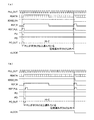
次に、受信側回路3の動作について、タイミングチャートを用いて説明する。図8(a)および図8(b)は、PLL12の出力信号PLL_OUTが受信データ信号RDATAに同期していない場合(同期確立していない場合)の信号波形を示したタイミングチャートである。また、図8(a)は、PLL12の出力信号PLL_OUTの位相が進んでいる場合を示しており、図8(b)は、PLL12の出力信号PLL_OUTの位相が遅れている場合を示している。
Next, the operation of the
図8(a)に示すように、リファレンス・基準信号発生器21aにおけるOR回路35の出力信号EDGE_ENは、PLL12の出力信号PLL_OUTと受信データ信号RDATAとが同期していない場合には、PLLロック信号nLOCKが「H」なので、常に「H」となっている。
As shown in FIG. 8A, the output signal EDGE_EN of the
このため、リファレンス・基準信号発生器21aにおけるAND回路36の入力端子Bには「H」が入力されているので、リファレンス信号REF_Rの立ち上がりおよび立ち下がりは、受信データ信号RDATAの立ち上がりおよび立ち下がりと一致している。図8(a)では、受信データ信号RDATAが同期パターンSYNCである場合を示しており、この場合、リファレンス信号REF_Rは、スタートビットからの12ビットが「H」、その後の12ビットが「L」となる。
Therefore, since “H” is input to the input terminal B of the AND
また、基準信号REF_PLLの立ち上がりはPLL12の出力信号PLL_OUTの立ち下がりと一致しており、基準信号REF_PLLの立ち上がりは、PLL12の出力信号PLL_OUTの次の立ち下がりと一致している。なお、基準信号REF_PLLは、出力信号PLL_OUTの1パルス(1周期)分だけ「H」となっており、その立ち上がりおよび立ち下がりは、出力信号PLL_OUTの立ち下がりと一致している。
The rising edge of the reference signal REF_PLL coincides with the falling edge of the output signal PLL_OUT of the
そして、リファレンス信号REF_Rの立ち上がり前に基準信号REF_PLLの立ち上がりがあった場合、位相比較器23におけるNAND回路51の出力信号PUが「H」から「L」に切り替わる。その後、リファレンス信号REF_Rの立ち上がりがあると、NAND回路51の出力信号PUが「L」から「H」に戻る。これにより、受信データ信号RDATAの位相と、PLL12の出力信号PLL_OUTの位相との位相差が検出される。なお、位相比較器23におけるNAND回路52の出力信号PDは、この間「H」のままとなっている。そして、これにより、位相比較器23(位相比較部40)からの出力信号PC_OUTは、NAND回路51の出力信号PUが「L」になっている期間だけ、ハイインピーダンス(Hi−Z)状態から「H」に切り替わる。
When the reference signal REF_PLL rises before the reference signal REF_R rises, the output signal PU of the
なお、図8(a)の例では、PLL12の出力信号PLL_OUTの位相が、受信データ信号RDATAの位相に対して、半クロック以上進んでいる。このように、PLL12の出力信号PLL_OUTの位相が受信データ信号RDATAの位相に対して半クロック以上ずれている場合、送信されたデータを適切に受信することができない。したがって、適切な受信を行うためには、PLL12の出力信号PLL_OUTの位相を、受信データ信号RDATAの位相に対して、半クロック以内の誤差で同期させてロックすることが好ましい。
In the example of FIG. 8A, the phase of the output signal PLL_OUT of the
一方、図8(b)に示すように、基準信号REF_PLLの立ち上がりよりも前にリファレンス信号REF_Rの立ち上がりがあった場合、位相比較器23におけるNAND回路52の出力信号PDが「H」から「L」に切り替わる。その後、基準信号REF_PLLの立ち上がりがあると、NAND回路52の出力信号PDが「L」から「H」に戻る。これにより、受信データ信号RDATAの位相と、PLL12の出力信号PLL_OUTの位相との位相差が検出される。なお、位相比較器23におけるNAND回路51の出力信号PUは、この間「H」のままとなっている。そして、これにより、位相比較器23(位相比較部40)からの出力信号PC_OUTは、NAND回路52の出力信号PDが「L」になっている期間だけハイインピーダンス(Hi−Z)状態から「L」に切り替わる。
On the other hand, as shown in FIG. 8B, when the reference signal REF_R rises before the reference signal REF_PLL rises, the output signal PD of the
図9(a)および図9(b)は、PLL12の出力信号PLL_OUTが受信データ信号RDATAに同期していない状態から、同期している状態に移行する際(同期確立時)の信号波形を示したタイミングチャートである。なお、図9(a)は、PLL12の出力信号PLL_OUTの位相が、受信データ信号RDATAに対して半クロック以上進んでいる状態から、位相進みが半クロック以内となる場合を示している。また、図9(b)は、PLL12の出力信号PLL_OUTの位相が、受信データ信号RDATAに対して半クロック以上遅れている状態から、位相遅れが半クロック以内となる場合を示している。
FIGS. 9A and 9B show signal waveforms when the output signal PLL_OUT of the
図9(a)に示すように、PLL12の出力信号PLL_OUTと受信データ信号RDATAとが同期していない場合(両者の位相差が半クロック(受信データ信号RDATAの周期の1/2倍以上)以上の場合)には、PLLロック信号nLOCKが「L」なので、リファレンス・基準信号発生器21aにおけるOR回路35の出力信号EDGE_ENは常に「H」となっている。このため、リファレンス・基準信号発生器21aにおけるAND回路36の入力端子Bには「H」が入力されているので、リファレンス信号REF_Rの立ち上がりおよび立ち下がりは、受信データ信号RDATAの立ち上がりおよび立ち下がりと一致している。
As shown in FIG. 9A, when the output signal PLL_OUT of the
また、基準信号REF_PLLの立ち上がりはPLL12の出力信号PLL_OUTの立ち下がりと一致しており、基準信号REF_PLLの立ち上がりは、PLL12の出力信号PLL_OUTの次の立ち下がりと一致している。
The rising edge of the reference signal REF_PLL coincides with the falling edge of the output signal PLL_OUT of the
そして、受信データ信号RDATAのストップビットの受信を開始した後、リファレンス信号REF_Rの立ち上がり前に基準信号REF_PLLの立ち上がりがあった場合、位相比較器23におけるNAND回路51の出力信号PUが「H」から「L」に切り替わる。その後、リファレンス信号REF_Rの立ち上がりがあると、NAND回路51の出力信号PUが「L」から「H」に戻る。これにより、受信データ信号RDATAの位相と、PLL12の出力信号PLL_OUTの位相との位相差が検出される。なお、位相比較器23におけるNAND回路52の出力信号PDは、この間「H」のままとなっている。そして、これにより、位相比較器23(位相比較部40)からの出力信号PC_OUTは、NAND回路51の出力信号PUが「L」になっている期間だけ、ハイインピーダンス(Hi−Z)状態から「H」に切り替わる。
Then, after the reception of the stop bit of the reception data signal RDATA is started, when the reference signal REF_PLL rises before the reference signal REF_R rises, the output signal PU of the
そして、この位相比較器23からの出力信号PC_OUTは、LPF24を介してVCO25に入力され、VCO25では、PLL12の出力信号PLL_OUTの位相を遅らせて受信データ信号RDATAに同期させるように、発振周波数が制御される。
The output signal PC_OUT from the
その後、PLL12の出力信号PLL_OUTの24パルスごとに一回、上記と同様の位相差の検出作業が行われる。そして、PLL12の出力信号PLL_OUTと受信データ信号RDATAとの位相差が半クロック以内になった場合(同期が確立した場合)、PLL12の出力がロックされ、PLLロック信号nLOCKが「L」に切り替えられる。なお、これにより、リファレンス・基準信号発生器21aにおけるOR回路35の出力信号EDGE_ENは、シフトレジスタ30の出力が「H」の期間、すなわち、PLL12の出力信号PLL_OUTの1パルス分に相当する期間だけ、「H」となる。
Thereafter, the same phase difference detection operation as described above is performed once every 24 pulses of the output signal PLL_OUT of the
一方、図9(b)に示すように、基準信号REF_PLLの立ち上がりよりも前にリファレンス信号REF_Rの立ち上がりがあった場合、位相比較器23におけるNAND回路52の出力信号PDが「H」から「L」に切り替わる。その後、基準信号REF_PLLの立ち上がりがあると、NAND回路52の出力信号PDが「L」から「H」に戻る。これにより、受信データ信号RDATAの位相と、PLL12の出力信号PLL_OUTの位相との位相差が検出される。なお、位相比較器23におけるNAND回路51の出力信号PUは、この間「H」のままとなっている。そして、これにより、位相比較器23(位相比較部40)からの出力信号PC_OUTは、NAND回路51の出力信号PUが「L」になっている期間だけ、ハイインピーダンス(Hi−Z)状態から「H」に切り替わる。
On the other hand, as shown in FIG. 9B, when the reference signal REF_R rises before the reference signal REF_PLL rises, the output signal PD of the
そして、この位相比較器23からの出力信号PC_OUTは、LPF24を介してVCO25に入力され、VCO25ではPLL12の出力信号PLL_OUTの位相を進ませて受信データ信号RDATAに同期させるように、発振周波数が制御される。
The output signal PC_OUT from the
その後、PLL12の出力信号PLL_OUTの24パルスごとに一回、上記と同様の位相差の検出作業が行われる。そして、PLL12の出力信号PLL_OUTと受信データ信号RDATAとの位相差が半クロック以内になった場合(同期が確立した場合)、PLL12の出力がロックされ、PLLロック信号nLOCKが「L」に切り替えられる。なお、これにより、リファレンス・基準信号発生器21aにおけるOR回路35の出力信号EDGE_ENは、シフトレジスタ30の出力が「H」の期間、すなわち、PLL12の出力信号PLL_OUTの1パルス分に相当する期間だけ、「H」となる。
Thereafter, the same phase difference detection operation as described above is performed once every 24 pulses of the output signal PLL_OUT of the
図10(a)および図10(b)は、PLL12の出力信号PLL_OUTが受信データ信号RDATAに同期している場合(同期確立後、データ通信中の場合)の信号波形を示したタイミングチャートである。
FIGS. 10A and 10B are timing charts showing signal waveforms when the output signal PLL_OUT of the
リファレンス・基準信号発生器21aにおけるOR回路35の出力信号EDGE_ENは、PLL12の出力信号PLL_OUTが受信データ信号RDATAに同期しており、PLLロック信号nLOCKが「L」となっている場合、シフトレジスタ30の出力が「H」の期間、すなわち、PLL12の出力信号PLL_OUTの1パルス分に相当する期間だけ、「H」となる。
The output signal EDGE_EN of the
そして、OR回路35の出力信号EDGE_ENが「H」の期間中に受信データ信号RDATAの立ち上がり(「0」から「1」への変化)があると、AND回路36の出力が「H」となり、リファレンス信号REF_Rが「H」に切り替わる。なお、フリップフロップ37のリセット端子RBには1段目のフリップフロップ32の出力が反転されて入力されるので、リファレンス信号REF_Rは、「H」に切り替わった後、PLL12の出力信号PLL_OUTのパルスが2回発生したときに、「L」に戻される。
If the reception data signal RDATA rises (changes from “0” to “1”) while the output signal EDGE_EN of the
また、基準信号REF_PLLは、シフトレジスタ30の出力が「H」の期間中に、PLL12の出力信号PLL_OUTの立ち下がりがあった場合に、「H」となる。そして、その次のPLL12の出力信号PLL_OUTの立ち下がりで「L」に戻る。
Further, the reference signal REF_PLL becomes “H” when the output signal PLL_OUT of the
そして、図10(a)に示すように、基準信号REF_PLLの立ち上がりが、リファレンス信号REF_Rの立ち上がりよりも早い場合、位相比較器23に備えられているNAND回路51の出力信号PUが、基準信号REF_PLLの立ち上がりと同時に「L」となり、リファレンス信号REF_Rの立ち上がりと同時に「H」に戻る。そして、NAND回路51の出力信号PUが、「L」の期間中、位相比較器23の出力信号PC_OUTがハイインピーダンス状態から「H」に切り替わる。これにより、シリアル伝送装置1では、受信データ信号RDATAの位相とPLL12の出力信号PLL_OUTの位相とのずれを小さくするようにVCO25を制御する。
As shown in FIG. 10A, when the rising edge of the reference signal REF_PLL is earlier than the rising edge of the reference signal REF_R, the output signal PU of the
一方、図10(b)に示すように、リファレンス信号REF_Rの立ち上がりが、基準信号REF_PLLの立ち上がりよりも早い場合、位相比較器23に備えられているNAND回路52の出力信号PDが、リファレンス信号REF_Rの立ち上がりと同時に「L」となり、基準信号REF_PLLの立ち上がりと同時に「H」に戻る。そして、NAND回路52の出力信号PDが、「L」の期間中、位相比較器23の出力信号PC_OUTがハイインピーダンス状態から「L」に切り替わる。これにより、シリアル伝送装置1では、受信データ信号RDATAの位相とPLL12の出力信号PLL_OUTの位相とのずれを小さくするようにVCO25を制御する。
On the other hand, as shown in FIG. 10B, when the rising edge of the reference signal REF_R is earlier than the rising edge of the reference signal REF_PLL, the output signal PD of the
また、リファレンス信号REF_Rの立ち上がりと、基準信号REF_PLLの立ち上がりとの差(受信データ信号RDATAとPLL12の出力信号PLL_OUTとの位相差)が半クロック以内の場合、PLLロック信号nLOCKは引き続き「L」とされ、PLL12のロックが継続される。
When the difference between the rising edge of the reference signal REF_R and the rising edge of the reference signal REF_PLL (the phase difference between the reception data signal RDATA and the output signal PLL_OUT of the PLL 12) is within half a clock, the PLL lock signal nLOCK continues to be “L”. Then, the lock of the
図11(a)および図11(b)は、PLL12の出力信号PLL_OUTが受信データ信号RDATAに同期している状態から、同期が外れる状態に移行する際(同期が外れた時)の信号波形を示したタイミングチャートである。
FIG. 11A and FIG. 11B show signal waveforms when the output signal PLL_OUT of the
リファレンス・基準信号発生器21aにおけるOR回路35の出力信号EDGE_ENは、PLL12の出力信号PLL_OUTが受信データ信号RDATAに同期しており、PLLロック信号nLOCKが「L」となっている場合、シフトレジスタ30の出力が「H」の期間、すなわち、PLL12の出力信号PLL_OUTの1パルス分に相当する期間だけ、「H」となる。
The output signal EDGE_EN of the
そして、OR回路35の出力信号EDGE_ENが「H」の期間中に受信データ信号RDATAの立ち上がり(「0」から「1」への変化)があると、AND回路36の出力が「H」となり、リファレンス信号REF_Rが「H」に切り替わる。なお、フリップフロップ37のリセット端子RBには1段目のフリップフロップ32の出力が反転されて入力されるので、リファレンス信号REF_Rは、「H」に切り替わった後、PLL12の出力信号PLL_OUTのパルスが2回発生したときに、「L」に戻される。
If the reception data signal RDATA rises (changes from “0” to “1”) while the output signal EDGE_EN of the
また、基準信号REF_PLLは、シフトレジスタ30の出力が「H」の期間中に、PLL12の出力信号PLL_OUTの立ち下がりがあった場合に、「H」となる。そして、その次のPLL12の出力信号PLL_OUTの立ち下がりで「L」に戻る。
Further, the reference signal REF_PLL becomes “H” when the output signal PLL_OUT of the
そして、図11(a)に示すように、基準信号REF_PLLの立ち上がりが、リファレンス信号REF_Rの立ち上がりよりも早い場合、位相比較器23に備えられているNAND回路51の出力信号PUが、基準信号REF_PLLの立ち上がりと同時に「L」となり、リファレンス信号REF_Rの立ち上がりと同時に「H」に戻る。そして、NAND回路51の出力信号PUが、「L」の期間中、位相比較器23の出力信号PC_OUTがハイインピーダンス状態から「H」に切り替わる。
As shown in FIG. 11A, when the rising edge of the reference signal REF_PLL is earlier than the rising edge of the reference signal REF_R, the output signal PU of the
そして、リファレンス信号REF_Rの立ち上がりと、基準信号REF_PLLの立ち上がりとの差(受信データ信号RDATAとPLL12の出力信号PLL_OUTとの位相差)が半クロック以内の場合、PLLロック信号nLOCKは引き続き「L」とされ、PLL12のロックが継続される。
When the difference between the rising edge of the reference signal REF_R and the rising edge of the reference signal REF_PLL (the phase difference between the reception data signal RDATA and the output signal PLL_OUT of the PLL 12) is within half a clock, the PLL lock signal nLOCK continues to be “L”. Then, the lock of the
一方、受信データ信号RDATAとPLL12の出力信号PLL_OUTとの位相差が半クロック以上になった場合、PLL12のロックが外れ、PLLロック信号nLOCKは「H」に切り替えられる。
On the other hand, when the phase difference between the received data signal RDATA and the output signal PLL_OUT of the
また、図11(b)に示すように、リファレンス信号REF_Rの立ち上がりが、基準信号REF_PLLの立ち上がりよりも早い場合、位相比較器23に備えられているNAND回路52の出力信号PDが、リファレンス信号REF_Rの立ち上がりと同時に「L」となり、基準信号REF_PLLの立ち上がりと同時に「H」に戻る。そして、NAND回路52の出力信号PDが、「L」の期間中、位相比較器23の出力信号PC_OUTがハイインピーダンス状態から「L」に切り替わる。
Also, as shown in FIG. 11B, when the rising edge of the reference signal REF_R is earlier than the rising edge of the reference signal REF_PLL, the output signal PD of the
そして、受信データ信号RDATAとPLL12の出力信号PLL_OUTとの位相差が半クロック以内の場合、PLLロック信号nLOCKは引き続き「L」とされ、PLL12のロックが継続される。
When the phase difference between the received data signal RDATA and the output signal PLL_OUT of the
一方、受信データ信号RDATAとPLL12の出力信号PLL_OUTとの位相差が半クロック以上になった場合、PLL12のロックが外れ、PLLロック信号nLOCKは「H」に切り替えられる。
On the other hand, when the phase difference between the received data signal RDATA and the output signal PLL_OUT of the
以上のように、本実施形態にかかるシリアル伝送装置1は、データ信号またはコマンド信号の送信側回路2から受信側回路3への伝送を開始する前に、データ信号およびコマンド信号を伝送する信号線と共通の信号線を用いて、データ信号およびコマンド信号と同じデータ長で、かつ、スタートビットとストップビットとが異なる値からなる同期パターンSYNCを伝送する。そして、受信側回路3では、PLL12が、出力信号PLL_OUTの位相を、受信器10Rによって受信した受信データ信号RDATAに含まれる同期パターンSYNCに基づいて制御することにより、データ信号およびコマンド信号の位相に同期させる。
As described above, the serial transmission device 1 according to the present embodiment has the signal line for transmitting the data signal and the command signal before starting the transmission of the data signal or the command signal from the
これにより、シリアル伝送装置1では、クロック信号を送信することなく、上記データ信号および上記コマンド信号と共通の信号線によって送信される同期パターンに基づいて、受信側回路3を送信側回路2に同期させることができる。したがって、送信側回路2と受信側回路3との間で、ノイズや静電気等の外乱に対する信頼性の高い信号伝送を行うことができる。また、クロック信号を伝送するための専用の信号線を備える必要がないので、装置構成の簡略化、小型化を図ることができる。
As a result, the serial transmission device 1 synchronizes the
また、シリアル伝送装置1では、受信側回路3に備えられるPLL12が、受信データ信号RDATAの位相とPLL12の出力信号PLL_OUTの位相とを同期させて固定し、PLLロック信号nLOCKを「L」にする(同期が確立したことを示す信号を送信側回路2に送信する)。そして、送信側回路2は、同期が確立した後に、コマンド信号またはデータ信号の伝送を開始する。
Further, in the serial transmission device 1, the
より詳細には、PLL12に備えられる位相比較器23内のPLLロック信号生成部41が、受信データ信号RDATA(同期パターンSYNC)とPLL12の出力信号PLL_OUTとの同期を検出し、同期が確立した場合に、送信側回路2に備えられるタイミング制御回路8に送信しているPLLロック信号nLOCKを「H」から「L」に切り替える。そして、送信側回路2では、PLLロック信号nLOCKが「L」に切り替えられた後に、コマンド信号またはデータ信号の伝送を開始する。
More specifically, when the PLL lock
これにより、シリアル伝送装置1では、送信側回路2と受信側回路3とが確実に同期している状態で、コマンド信号およびデータ信号の伝送を行うことができる。
Thereby, in the serial transmission device 1, the command signal and the data signal can be transmitted in a state where the
また、シリアル伝送装置1では、上記データ信号または上記コマンド信号を送信していない期間は、同期パターンSYNCの送信側回路2から受信側回路3への送信を継続する。これにより、受信側回路3におけるPLL12において、同期パターンSYNCに基づくPLL12の出力信号PLL_OUTと受信データ信号RDATAとの同期を継続的に行い、また、同期したPLL12の出力信号PLL_OUTの位相をロックして、同期状態を保つことができる。
Further, in the serial transmission device 1, the transmission of the synchronization pattern SYNC from the
また、シリアル伝送装置1では、コマンド信号またはデータ信号を伝送している期間中、伝送しているコマンド信号またはデータ信号を用いて、受信データ信号RDATAとPLL12の出力信号PLL_OUTとの同期状態を検出する。
Further, the serial transmission device 1 detects the synchronization state between the received data signal RDATA and the output signal PLL_OUT of the
より詳細には、PLL12に備えられたリファレンス・基準信号発生器21a(リファレンス発生器21)が受信データ信号RDATAのスタートビットの立ち上がりと同時に立ち上がるリファレンス信号REF_Rを生成する。そして、リファレンス・基準信号発生器21a(基準信号発生器22)が、PLL12の出力信号PLL_OUTにおける特定のパルス(24パルス中の1パルス)の立ち下がりと同時に立ち上がる基準信号REF_PLLを生成する。そして、PLL12に備えられる位相比較器23内のPLLロック信号生成部41が、受信データ信号RDATA(データ信号またはコマンド信号)とPLL12の出力信号PLL_OUTとの同期を検出し、同期している場合には、送信側回路2に備えられるタイミング制御回路8に送信しているPLLロック信号nLOCKを「L」に保ち、同期が外れた場合には、送信側回路2に備えられるタイミング制御回路8に送信しているPLLロック信号nLOCKを「H」に切り替える(同期が外れたことを示す信号を生成して送信側回路2に送信する)。そして、同期状態が確保されている場合には、引き続きコマンド信号またはデータ信号の伝送を継続する。
More specifically, the reference /
これにより、データ信号またはコマンド信号の受信中に、PLL12の出力信号PLL_OUTと受信データ信号RDATA(データ信号またはコマンド信号)との同期が外れた場合、送信側回路2にそのことを通知することができる。このため、送信側回路2は、データ信号およびコマンド信号の送信を停止させ、同期パターンSYNCの送信を開始する。したがって、より信頼性の高い信号伝送を行うことができる。
As a result, if the output signal PLL_OUT of the
また、シリアル伝送装置1では、位相比較器23における位相比較部40が、上記のように生成されたリファレンス信号REF_Rの立ち上がりと基準信号REF_PLLの立ち上がりとを比較した結果に基づいて、受信データ信号RDATAの位相とPLL12の出力信号PLL_OUTの位相とのずれを小さくするようにVCO25の発振周波数と位相とを制御する。
Further, in the serial transmission device 1, the
これにより、シリアル伝送装置1では、データ信号またはコマンド信号と同時にクロック信号を伝送することなく、送信側回路2と受信側回路3とを適切に同期させた状態で、データ信号またはコマンド信号のシリアル伝送を行うことができる。したがって、クロック信号を伝送するための専用の信号線(差動対)を備える必要がないので、装置構成の簡略化、小型化を図ることができる。
As a result, the serial transmission device 1 does not transmit the clock signal simultaneously with the data signal or the command signal, and transmits the serial data signal or command signal in a state where the
また、シリアル伝送装置1では、送信側回路2から受信側回路3への伝送にLVDS方式を用いている。LVDS方式による信号伝送は、信号を送信している期間中と、送信していない期間中とで、消費電力がほとんど変わらないという特性がある。このため、シリアル伝送装置1では、データ信号またはコマンド信号を伝送していない期間中に、同期パターンを継続的に伝送しているが、同期パターンを伝送しない場合と消費電力はほとんど変わらない。
The serial transmission device 1 uses the LVDS method for transmission from the
なお、本実施形態では、20ビットの入力データ信号を伝送するために、スタートビット、同期パターン区別ビット、パリティビット、ストップビットを付加した24ビットの送信データ信号TDATAを生成して伝送する構成について説明したが、送信データ信号TDATA(受信データ信号RDATA)のデータサイズはこれに限るものではなく、入力データのデータサイズに応じて適宜決定すればよい。 In this embodiment, in order to transmit a 20-bit input data signal, a 24-bit transmission data signal TDATA to which a start bit, a synchronization pattern distinction bit, a parity bit, and a stop bit are added is generated and transmitted. As described above, the data size of the transmission data signal TDATA (reception data signal RDATA) is not limited to this, and may be appropriately determined according to the data size of the input data.
また、本実施形態では、同期パターンとして、前半の12ビットが「1」、後半の12ビットが「0」という構成の信号を用いたが、同期パターンの構成はこれに限るものではない。データ信号およびコマンド信号と同じデータ長を有し、スタートビットとストップビットとが異なる値からなるものであればよい。なお、同期パターンは、データ信号およびコマンド信号と区別できることが好ましい。また、同期パターンは、1シンボル(本実施形態では24ビット)中で、「1」と「0」との変化が1度だけある信号であることが好ましい。 In this embodiment, a signal having a configuration in which the first 12 bits are “1” and the second 12 bits is “0” is used as the synchronization pattern. However, the configuration of the synchronization pattern is not limited to this. The data signal and the command signal have the same data length as long as the start bit and the stop bit have different values. Note that the synchronization pattern is preferably distinguishable from the data signal and the command signal. Further, the synchronization pattern is preferably a signal in which there is only one change between “1” and “0” in one symbol (24 bits in the present embodiment).
また、本実施形態では、送信側回路2に備えられる送信器10Tと受信側回路3に備えられる受信器10Rとの間で、LVDS方式の伝送を行う場合について説明したが、これに限るものではない。例えば、LVDS方式以外の差動伝送方式で信号をシリアル伝送するものであってもよく、あるいは、差動伝送方式以外の伝送方法をもちいてもよい。
In the present embodiment, the case where LVDS transmission is performed between the transmitter 10T included in the
本発明は上述した実施形態に限定されるものではなく、請求項に示した範囲で種々の変更が可能である。すなわち、請求項に示した範囲で適宜変更した技術的手段を組み合わせて得られる実施形態についても本発明の技術的範囲に含まれる。 The present invention is not limited to the above-described embodiments, and various modifications can be made within the scope shown in the claims. That is, embodiments obtained by combining technical means appropriately changed within the scope of the claims are also included in the technical scope of the present invention.
本発明は、通信装置間あるいは集積回路等の電子部品間において、シリアル伝送方式でデータを伝送する装置全般に適用できる。 The present invention can be applied to all devices that transmit data by serial transmission between communication devices or between electronic components such as integrated circuits.
1 シリアル伝送装置
2 送信側回路(シリアル信号送信装置)
3 受信側回路(シリアル信号受信装置)
4 分周器
5 ラッチ回路
6 パラレルシリアル変換回路
7 シリアルデータ挿入回路
8 タイミング制御回路
9 同期パターン生成回路(同期パターン生成手段)
10T 送信器
10R 受信器
11 シリアルパラレル変換回路(信号判別手段)
12 PLL(位相固定手段)
13 タイミング制御回路
14P,14N 信号線
21 リファレンス発生器
21a リファレンス・基準信号発生器
22 基準信号発生器
23 位相比較器(同期検出手段、位相比較手段、固定通知手段)
24 LPF
25 VCO
40 位相比較部(同期検出手段、位相比較手段)
41 PLLロック信号生成部(同期検出手段、固定通知手段)
1
3 Receiver circuit (serial signal receiver)
4
12 PLL (phase locking means)
13
24 LPF
25 VCO
40 Phase comparison unit (synchronization detection means, phase comparison means)
41 PLL lock signal generator (synchronization detection means, fixed notification means)
Claims (14)
上記送信されるシリアル信号と同じデータ長で、かつ、スタートビットとストップビットとが異なる値からなる同期パターンを生成する同期パターン生成手段を備え、
上記シリアル信号と上記同期パターンとを、共通の信号線を用いて送信することを特徴とするシリアル信号送信装置。 A serial signal transmission device that converts an input data signal into a serial signal based on a clock signal and transmits the serial signal,
A synchronization pattern generating means for generating a synchronization pattern having the same data length as the serial signal to be transmitted and having different values of the start bit and the stop bit;
A serial signal transmitting apparatus, wherein the serial signal and the synchronization pattern are transmitted using a common signal line.
上記シリアル信号の伝送を開始することを特徴とする請求項1〜4のいずれか1項に記載のシリアル信号送信装置。 After transmitting the synchronization pattern, when receiving a fixed notification signal indicating that the synchronization of the destination device is established from the destination device,
The serial signal transmission apparatus according to claim 1, wherein transmission of the serial signal is started.
上記送信先の装置から当該送信先の装置の同期が確立したことを示す固定通知信号を受信した場合に、上記シリアルデータの送信を再開することを特徴とする、請求項1〜5のいずれか1項に記載のシリアル信号送信装置。 After the start of transmission of the serial signal, when receiving a lock release signal indicating that the transmission destination device is out of synchronization from the transmission destination device, it waits for transmission of the serial data and sets the synchronization pattern. Send
The transmission of the serial data is resumed when a fixed notification signal indicating that synchronization of the transmission destination device is established is received from the transmission destination device. Item 2. The serial signal transmission device according to item 1.
出力する信号の位相を制御して固定する位相固定手段を備え、
上記位相固定手段は、当該位相固定手段の出力する信号の位相を、上記シリアル信号と共通の信号線を介して受信する、上記シリアル信号と同じデータ長で、かつ、スタートビットとストップビットとが異なる値からなる同期パターンに基づいて制御することにより、上記シリアル信号の位相と同期させることを特徴とするシリアル信号受信装置。 A serial signal receiving device that converts a received serial signal into a parallel signal,
Phase fixing means for controlling and fixing the phase of the output signal;
The phase fixing means receives the phase of the signal output from the phase fixing means via a signal line common to the serial signal, has the same data length as the serial signal, and has a start bit and a stop bit. A serial signal receiving apparatus, wherein the serial signal is synchronized with the phase of the serial signal by controlling based on synchronization patterns having different values.
当該位相固定手段の出力する信号の位相が上記シリアル信号の位相と同期しているか否かを検出する同期検出手段と、
上記位相固定手段の出力する信号の位相が上記シリアル信号の位相と同期している場合に、そのこと示す固定通知信号を生成して上記シリアル信号の送信元の装置に送信する固定通知手段とを備えていることを特徴とする請求項7に記載のシリアル信号受信装置。 The phase locking means is
Synchronization detecting means for detecting whether or not the phase of the signal output from the phase fixing means is synchronized with the phase of the serial signal;
When the phase of the signal output from the phase fixing means is synchronized with the phase of the serial signal, a fixed notification means for generating a fixed notification signal indicating that and transmitting the fixed notification signal to the transmission source device of the serial signal; The serial signal receiving device according to claim 7, further comprising:
上記固定通知手段は、上記位相固定手段の出力する信号の位相と上記シリアル信号の位相との同期が外れた場合に、そのことを示す固定解除信号を生成して上記シリアル信号の送信元の装置に送信することを特徴とする請求項8または9に記載のシリアル信号受信装置。 The synchronization detection means compares the edge of a specific pulse in the signal output from the phase fixing means with the edge of the start bit of the serial signal during the period of receiving the serial signal, Detecting whether the phase of the signal output from the fixing means is synchronized with the phase of the serial signal,
When the phase of the signal output from the phase fixing unit and the phase of the serial signal are out of synchronization, the fixed notification unit generates a fixed release signal indicating the phase and transmits the serial signal from the device The serial signal receiving device according to claim 8 or 9, wherein
上記受信した信号がシリアル信号である場合のみ、上記パラレル信号を外部に出力することを特徴とする請求項7〜11のいずれか1項に記載のシリアル信号受信装置。 Comprising signal determining means for determining whether the received signal is the synchronization pattern or the serial signal;
The serial signal receiving apparatus according to claim 7, wherein the parallel signal is output to the outside only when the received signal is a serial signal.
上記送信されるシリアル信号と同じデータ長で、かつ、スタートビットとストップビットとが異なる値からなる同期パターンを生成するステップと、
上記同期パターンを、上記シリアル信号を伝送する信号線と共通の信号線を用いて送信するステップと、
上記位相固定手段の出力する信号の位相を、上記同期パターンに基づいて制御することにより、上記シリアル信号の位相と同期させるステップと、を含むことを特徴とするシリアル信号伝送方法。 The input data signal is converted into a serial signal based on the clock signal and transmitted from the serial signal transmission device, and the transmission is performed by the serial signal reception device having phase fixing means for controlling and fixing the phase of the output signal. A serial transmission method for receiving a received serial signal and converting it into a parallel signal,
Generating a synchronization pattern having the same data length as the serial signal to be transmitted and having different values of the start bit and the stop bit;
Transmitting the synchronization pattern using a signal line common to the signal line for transmitting the serial signal;
A step of synchronizing the phase of the signal output from the phase fixing means with the phase of the serial signal by controlling the phase of the signal based on the synchronization pattern.
Priority Applications (1)
| Application Number | Priority Date | Filing Date | Title |
|---|---|---|---|
| JP2004256258A JP4335101B2 (en) | 2004-09-02 | 2004-09-02 | Serial signal transmitting device, serial signal receiving device, serial transmission device, serial transmission method |
Applications Claiming Priority (1)
| Application Number | Priority Date | Filing Date | Title |
|---|---|---|---|
| JP2004256258A JP4335101B2 (en) | 2004-09-02 | 2004-09-02 | Serial signal transmitting device, serial signal receiving device, serial transmission device, serial transmission method |
Publications (2)
| Publication Number | Publication Date |
|---|---|
| JP2006074524A true JP2006074524A (en) | 2006-03-16 |
| JP4335101B2 JP4335101B2 (en) | 2009-09-30 |
Family
ID=36154629
Family Applications (1)
| Application Number | Title | Priority Date | Filing Date |
|---|---|---|---|
| JP2004256258A Expired - Fee Related JP4335101B2 (en) | 2004-09-02 | 2004-09-02 | Serial signal transmitting device, serial signal receiving device, serial transmission device, serial transmission method |
Country Status (1)
| Country | Link |
|---|---|
| JP (1) | JP4335101B2 (en) |
Cited By (5)
| Publication number | Priority date | Publication date | Assignee | Title |
|---|---|---|---|---|
| JP2008165238A (en) * | 2007-01-03 | 2008-07-17 | Samsung Electronics Co Ltd | Serialized video data processing method and apparatus for display |
| WO2010023794A1 (en) * | 2008-08-29 | 2010-03-04 | パナソニック株式会社 | Interface communication device |
| JP2016152576A (en) * | 2015-02-19 | 2016-08-22 | 株式会社メガチップス | Data transmission device, transmitter and receiver |
| JP2016163246A (en) * | 2015-03-04 | 2016-09-05 | ザインエレクトロニクス株式会社 | Transmission device, reception device and transmission/reception system |
| JP2020068458A (en) * | 2018-10-24 | 2020-04-30 | ザインエレクトロニクス株式会社 | Receiving device and transmission/reception system |
-
2004
- 2004-09-02 JP JP2004256258A patent/JP4335101B2/en not_active Expired - Fee Related
Cited By (8)
| Publication number | Priority date | Publication date | Assignee | Title |
|---|---|---|---|---|
| JP2008165238A (en) * | 2007-01-03 | 2008-07-17 | Samsung Electronics Co Ltd | Serialized video data processing method and apparatus for display |
| WO2010023794A1 (en) * | 2008-08-29 | 2010-03-04 | パナソニック株式会社 | Interface communication device |
| JP2016152576A (en) * | 2015-02-19 | 2016-08-22 | 株式会社メガチップス | Data transmission device, transmitter and receiver |
| JP2016163246A (en) * | 2015-03-04 | 2016-09-05 | ザインエレクトロニクス株式会社 | Transmission device, reception device and transmission/reception system |
| JP2020068458A (en) * | 2018-10-24 | 2020-04-30 | ザインエレクトロニクス株式会社 | Receiving device and transmission/reception system |
| WO2020085171A1 (en) * | 2018-10-24 | 2020-04-30 | ザインエレクトロニクス株式会社 | Reception device and transmission and reception system |
| US11646862B2 (en) | 2018-10-24 | 2023-05-09 | Thine Electronics, Inc. | Reception device and transmission and reception system |
| JP7280587B2 (en) | 2018-10-24 | 2023-05-24 | ザインエレクトロニクス株式会社 | Receiving device and transmitting/receiving system |
Also Published As
| Publication number | Publication date |
|---|---|
| JP4335101B2 (en) | 2009-09-30 |
Similar Documents
| Publication | Publication Date | Title |
|---|---|---|
| TWI410791B (en) | Apparatus and method for transmitting and receiving data bits | |
| US7340655B2 (en) | Skew adjustment circuit, skew adjustment method, data synchronization circuit, and data synchronization method | |
| US7134056B2 (en) | High-speed chip-to-chip communication interface with signal trace routing and phase offset detection | |
| JP2008236738A (en) | Protocol-agnostic automatic rate negotiation for high-speed serial interface in programmable logic device | |
| EP0186462B1 (en) | A method for detection of manchester-encoded signals | |
| JPH0773220B2 (en) | Device for converting serial data pattern signals | |
| JPH11514765A (en) | Method and system for resynchronizing a phase-shifted received data stream using a master clock | |
| US20040205416A1 (en) | Communication apparatus with failure detect function | |
| JPH0787447B2 (en) | System utilizing synchronous serial transmission medium | |
| JPH0783382B2 (en) | Method for converting a high speed serial data pattern input signal to a parallel data pattern output | |
| GB2109206A (en) | Data transmission system utilising power line of 3-phase alternating current | |
| JP4335101B2 (en) | Serial signal transmitting device, serial signal receiving device, serial transmission device, serial transmission method | |
| JP2005506798A (en) | Transition detection, validation and memory circuit | |
| KR100998773B1 (en) | System and method for generating deserialization timing signals | |
| CN107533533B (en) | Communication between integrated circuits | |
| EP1946475B1 (en) | Data interface and method of seeking synchronization | |
| EP0666662A1 (en) | Serial data clock receiver circuit and method therefor | |
| EP1306999A2 (en) | Data extraction circuit used for serial transmission of data signals between communication devices having different clock signal sources | |
| US7894562B2 (en) | Data message sync pattern | |
| CN101682500A (en) | Timing recovery circuit, communication node, network system, and electronic device | |
| US7660364B2 (en) | Method of transmitting serial bit-stream and electronic transmitter for transmitting a serial bit-stream | |
| KR101272886B1 (en) | apparatus and method for transmitting data with clock information | |
| JPH07288516A (en) | Serial data transmission / reception circuit | |
| US20080240320A1 (en) | Transmit clock generator | |
| JP3157029B2 (en) | Data receiving device |
Legal Events
| Date | Code | Title | Description |
|---|---|---|---|
| A621 | Written request for application examination |
Free format text: JAPANESE INTERMEDIATE CODE: A621 Effective date: 20060912 |
|
| A977 | Report on retrieval |
Free format text: JAPANESE INTERMEDIATE CODE: A971007 Effective date: 20081008 |
|
| A131 | Notification of reasons for refusal |
Free format text: JAPANESE INTERMEDIATE CODE: A131 Effective date: 20081014 |
|
| A521 | Written amendment |
Free format text: JAPANESE INTERMEDIATE CODE: A523 Effective date: 20081128 |
|
| RD02 | Notification of acceptance of power of attorney |
Free format text: JAPANESE INTERMEDIATE CODE: A7422 Effective date: 20081128 |
|
| TRDD | Decision of grant or rejection written | ||
| A01 | Written decision to grant a patent or to grant a registration (utility model) |
Free format text: JAPANESE INTERMEDIATE CODE: A01 Effective date: 20090623 |
|
| A01 | Written decision to grant a patent or to grant a registration (utility model) |
Free format text: JAPANESE INTERMEDIATE CODE: A01 |
|
| A61 | First payment of annual fees (during grant procedure) |
Free format text: JAPANESE INTERMEDIATE CODE: A61 Effective date: 20090624 |
|
| FPAY | Renewal fee payment (event date is renewal date of database) |
Free format text: PAYMENT UNTIL: 20120703 Year of fee payment: 3 |
|
| R150 | Certificate of patent or registration of utility model |
Free format text: JAPANESE INTERMEDIATE CODE: R150 |
|
| FPAY | Renewal fee payment (event date is renewal date of database) |
Free format text: PAYMENT UNTIL: 20120703 Year of fee payment: 3 |
|
| FPAY | Renewal fee payment (event date is renewal date of database) |
Free format text: PAYMENT UNTIL: 20130703 Year of fee payment: 4 |
|
| LAPS | Cancellation because of no payment of annual fees |