JP2005017221A - Substrate inspecting method and device therefor - Google Patents
Substrate inspecting method and device therefor Download PDFInfo
- Publication number
- JP2005017221A JP2005017221A JP2003185532A JP2003185532A JP2005017221A JP 2005017221 A JP2005017221 A JP 2005017221A JP 2003185532 A JP2003185532 A JP 2003185532A JP 2003185532 A JP2003185532 A JP 2003185532A JP 2005017221 A JP2005017221 A JP 2005017221A
- Authority
- JP
- Japan
- Prior art keywords
- inspection
- substrate
- wiring
- wiring patterns
- point
- Prior art date
- Legal status (The legal status is an assumption and is not a legal conclusion. Google has not performed a legal analysis and makes no representation as to the accuracy of the status listed.)
- Pending
Links
- 239000000758 substrate Substances 0.000 title claims abstract description 70
- 238000000034 method Methods 0.000 title claims description 26
- 238000007689 inspection Methods 0.000 claims abstract description 317
- 239000000523 sample Substances 0.000 abstract description 57
- 230000003247 decreasing effect Effects 0.000 abstract 1
- 238000013500 data storage Methods 0.000 description 20
- 239000004020 conductor Substances 0.000 description 19
- 230000008569 process Effects 0.000 description 16
- 230000008707 rearrangement Effects 0.000 description 13
- 238000001514 detection method Methods 0.000 description 12
- 230000002950 deficient Effects 0.000 description 8
- 239000007787 solid Substances 0.000 description 8
- 238000010586 diagram Methods 0.000 description 7
- 238000005259 measurement Methods 0.000 description 6
- 239000004973 liquid crystal related substance Substances 0.000 description 3
- 230000007423 decrease Effects 0.000 description 2
- 230000007547 defect Effects 0.000 description 2
- 230000000694 effects Effects 0.000 description 2
- 238000009413 insulation Methods 0.000 description 2
- 230000007246 mechanism Effects 0.000 description 2
- 230000009467 reduction Effects 0.000 description 2
- 230000004044 response Effects 0.000 description 2
- 239000004065 semiconductor Substances 0.000 description 2
- 239000000969 carrier Substances 0.000 description 1
- 238000009429 electrical wiring Methods 0.000 description 1
- 230000006870 function Effects 0.000 description 1
Images


Landscapes
- Testing Of Short-Circuits, Discontinuities, Leakage, Or Incorrect Line Connections (AREA)
Abstract
Description
【0001】
【発明の属する技術分野】
本発明は、プリント配線基板のような基板の配線における断線の有無や配線パターン間の短絡の有無の検査、所謂、配線の導通・短絡等の複数の検査を行う検査装置に関する。尚、この発明は、プリント配線基板に限らず、フレキシブル基板、多層配線基板、液晶ディスプレイやプラズマディスプレイ用の電極板、ならびに半導体パッケージ用のフィルムキャリアなど種々の基板上の電気的配線の検査に適用でき、この明細書では、それら種々の配線基板を総称して「基板」と称する。
【0002】
【従来の技術】
従来、プリント配線基板や、ICパッケージに用いられるパッケージ基板等の基板に形成された配線、スルーホール、ビヤ等の接続配線や、接続配線にICパッケージや半導体チップなどを接続するためのランドやパッドなどの導体パターン(以下、配線パターンと称する)における配線の導通や、配線パターンの間での短絡を検査する基板検査装置が知られている。このような検査装置において、検査対象の配線パターンの2箇所に設けられた検査点に、互いに独立して移動可能な一対の検査用接触子をそれぞれ一つずつ接触させて、検査を行うようにされたものが知られている。
【0003】
このような一対の検査用接触子を用いた基板検査装置において、検査を効率的に行うべく、一対の検査用接触子を順次配線上の検査点に接触させ、接触子間の検査対象配線の抵抗値に基づいてその配線パターンが導通していることを検査する導通検査を行った後、またはその前に、基板のほぼ全体に電源やグラウンドを供給することを目的として面状に形成されたベタ導体部又は基板とは別に基板の配線パターン全てをカバーするように設けられた導電性基準面と検査対象配線パターンとの間の静電容量に基づいて検査対象配線パターンと他の配線パターンとの間の短絡が無いことを検査する静電容量検査等、複数の種類の検査を行うことができる検査装置が提案されている(例えば、特許文献1参照。)。
【0004】
【特許文献1】
特公平4−17394号公報
【0005】
【発明が解決しようとする課題】
しかし、上記従来の検査装置では、ベタ導体または導電性基準面を用いて配線パターン間の短絡の有無の検査を行うことにより、短絡検査における各検査用接触子の移動を非常に減少させているが、検査を行うために各検査用接触子を検査点の位置に移動させる回数はかなり多い。また、検査用接触子を検査点の位置に移動させる動作には時間がかかるため、検査用接触子の移動回数が多いと、基板の検査工数が増大するという不都合があった。
【0006】
本発明は上記事情に鑑みてなされたもので、複数の種類の検査を行うときの検査用接触子の移動回数を少なくし、検査工数を低減した基板検査装置を提供することを目的とする。
【0007】
【課題を解決するための手段】
請求項1に記載の発明は、基板に形成された複数の配線パターンに対して所定の順序で、少なくとも二つの移動可能な検査用接触子を用いて、基板における配線の断線の有無及び配線パターン間の短絡の有無等の複数種類の検査を行う基板検査方法であって、前記配線パターンそれぞれについて検査を行うために設定された検査点のうち一つを代表検査点とし、前記配線パターンそれぞれについて、前記代表検査点に前記検査用接触子の一方を位置させた状態で、前記複数種類の検査を行うことを特徴としている。請求項1に記載の発明によれば、各配線パターンについて、当該配線パターンの代表検査点に検査用接触子の一方を位置させた状態で、複数種類の検査が行われる。
【0008】
請求項2に記載の発明は、請求項1記載の基板検査方法において、前記検査用接触子のうちの一つを前記代表検査点に位置させた状態のまま、他の検査用接触子を先発配線パターンの前記代表検査点以外の検査点に順次位置させて配線における断線の有無の検査を行うと共に、複数の配線パターンをカバーする導電面と代表検査点に一つの接触子が位置している配線パターンとの間の静電容量から配線パターン間の短絡の有無を検査することを特徴とする。請求項2に記載の発明によれば、前記検査用接触子のうちの一つを代表検査点に位置させた状態のまま、断線の有無及び短絡の有無の検査が行われるので、一つの検査用接触子の移動回数が少なくなる。
【0009】
請求項3に記載の発明は、請求項2記載の基板検査方法において、前記他の検査用接触子を移動させる間に、前記代表検査点に位置させた検査用接触子と前記導電面に電気的に接続された接点を用いて前記短絡の有無の検査を行うことを特徴とする。請求項3記載の発明によれば、前記他の検査用接触子を移動させる間に短絡の有無の検査が行われるので、更に検査工数が少なくなる。
【0010】
請求項4に記載の発明は、基板に形成された複数の配線パターンに対して、所定の順序で基板における配線の断線の有無及び配線パターン間の短絡の有無等の複数種類の検査を行う基板検査装置であって、少なくとも二つの移動可能な検査用接触子と、前記配線パターンそれぞれについて検査を行うために設定された検査点のうちの一つである代表検査点を記憶する代表検査点記憶部と、前記配線パターンそれぞれについて、前記代表検査点に前記検査用接触子の一方を位置させた状態で、前記複数種類の検査を行う検査動作制御部とを備えることを特徴としている。請求項4に記載の発明によれば、各配線パターンについて、当該配線パターンの代表検査点に検査用接触子の一方を位置させた状態で、複数種類の検査が行われる。
【0011】
【発明の実施の形態】
以下、本発明に係る実施形態を図面に基づいて説明する。図1は、本発明の一実施形態に係る基板検査装置1の構成の一例を説明するための図である。図1に示す基板検査装置1は、プローブ2,3と、抵抗値検出部4と、静電容量検出部5と、位置決め制御部6,7と、検査制御部8と、操作表示部9と、クリップ10とを備える。また、図1に示す基板100は、検査の対象となるプリント配線基板の一例であり、基板表面に形成された配線層101,102と、基板の内層に形成された配線層103を備えている。また、配線層103には、基板100の全体に例えば電源やグラウンドを供給するためのベタ導体部104が配線層101,102上の配線の全体をカバーするように面状に設けられている。
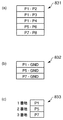
【0012】
図2は、基板100を、配線層101側から見た正面図である。図2に示す基板100の配線層101には、例えばIC(Integrated Circuit)の接続端子を接続するためのパッドP1〜P8(検査点)が形成されている。さらに、配線層101には、パッドP1,P2,P3,P4の間を相互に接続する配線パターンN1と、パッドP5とパッドP6とを接続する配線パターンN2と、パッドP7とパッドP8とを接続する配線パターンN3と、図略のバイアホール等により配線層103に接続された導体パターン105(共通検査点)とが形成されている。また、配線パターンN1,N2,N3は、ベタ導体部104と重なって対向する位置に形成されている。
【0013】
プローブ2,3は、それぞれ独立してX軸、Y軸及びZ軸方向へ駆動する図略の駆動機構に支持されており、それぞれ位置決め制御部6,7からの制御信号に応じてX軸、Y軸及びZ軸方向に移動制御される。位置決め制御部6,7は、例えば公知のNC(Numeric Control)制御装置により構成されており、検査制御部8から出力された座標データに応じて前記駆動機構を駆動させる。これにより、プローブ2,3は、所定の検査位置に位置決めされた被検査基板100の平面と平行な平面上の座標を規定する、X軸、Y軸方向に移動されて、被検査基板100上の所定測定点に相当する位置に移動された後、被検査基板100に向かうZ軸方向に駆動される。プローブ2,3が、被検査基板100上の測定点に当接し、弾性的に接触することにより、被検査基板100上の任意の2測定点の間の抵抗値の測定やプローブ2が接触している配線パターンとベタ導体部との間の静電容量の測定が行われる。
【0014】
抵抗値検出部4は、プローブ2とプローブ3との間の抵抗値を測定すると共にその測定した抵抗値を表すデータを検査制御部8へ出力する。静電容量検出部5には、プローブ2及びクリップ10が接続されており、検査制御部8からの制御信号に応じて、プローブ2とクリップ10との間の静電容量を測定する。そして、静電容量検出部5は、その測定した静電容量を表すデータを検査制御部8へ出力する。また、ユーザーが、導体パターン105をクリップ10で挟みこむことにより、導体パターン105と静電容量検出部5とが接続される。
【0015】
操作表示部9は、例えばキースイッチと液晶表示器あるいはタッチパネル式液晶表示器等から構成され、ユーザーからの検査の実行指示等の操作指示を受け付けて、その操作指示を検査制御部8へ出力したり、検査制御部8からの制御信号に応じて基板の検査結果を表示したりする。
【0016】
検査制御部8は、基板検査装置1全体の動作を司るもので、例えば基板検査装置1の動作を制御するための制御プログラム等を記憶するROM(Read Only Memory)、一時的にデータを保管するRAM(Random Access Memory)、及び制御プログラム等をROMから読み出して実行するマイクロコンピュータ等から構成されている。
【0017】
そして、検査制御部8は、所定の検査プログラムを実行することにより、検査対象の配線パターンの抵抗値に基づいてその配線パターンが導通していることを検査する導通検査、及び検査対象の配線パターンと導体パターン105との間の静電容量に基づいて検査対象の配線パターンと他の配線パターンとの間の短絡が無いことを検査する静電容量検査を実行する。また、検査制御部8は、基板データ記憶部81、基準容量データ記憶部82、検査箇所データ記憶部83、及び検査順序記憶部85を備える。さらに、検査制御部8は、所定のプログラムを実行することにより、並替え処理部84として機能する。
【0018】
基板データ記憶部81は、検査対象となる基板100に形成されたパッドP1〜P8、及び導体パターン105の座標位置を示す座標データや、パッドP1〜P8相互間の電気的な接続関係によって配線パターンN1,N2,N3を表したネットデータ等を記憶する。例えば、本実施例の基板100の場合、配線パターンN1,N2,N3を表すネットデータはそれぞれ、例えば、N1(P1,P2,P3,P4)、N2(P5,P6)、N3(P7,P8)として基板データ記憶部81に記憶されている。
【0019】
基準容量データ記憶部82は、静電容量検出部5により測定された静電容量から検査対象となる配線パターン等の良否判定を行うための基準となる静電容量データを記憶する。例えば、複数の良品の基板100において、配線パターンN1,N2,N3とベタ導体部104との間の静電容量を予め測定すると共に、その測定値から配線パターンN1,N2,N3が良品であると判断するための静電容量の範囲を取得しておく。そして、その静電容量の範囲が配線パターンN1,N2,N3それぞれの良否判定用静電容量データとして基準容量データ記憶部82に記憶されている。
【0020】
検査箇所データ記憶部83は、導通検査と静電容量検査とを行うための検査点を示す検査箇所データを、各検査の種類毎に記憶している。また、検査箇所データ記憶部83は、各配線パターンに含まれるパッドのうちの一つをヘッド(代表検査点)とし、このヘッドを示すデータをヘッドデータとして記憶している。
【0021】
図3は、検査箇所データ記憶部83に記憶されている検査箇所データ及びヘッドデータの一例を示す図である。図3(a)は導通検査を行うための検査箇所を示したデータテーブルの一例である導通検査点テーブル831を示しており、例えば「P1−P2」は、プローブ2とプローブ3とをそれぞれパッドP1とパッドP2とに接触させて、導通検査を行うべきことを示している。
【0022】
また、図3(b)は静電容量検査を行うための検査箇所を示すデータテーブルの一例である容量検査点テーブル832を示しており、例えば「P1−GND」は、プローブ2をパッドP1に接触させて、プローブ2と、導体パターン105に接続されているクリップ10とを用いて静電容量検査を行うべきことを示している。
【0023】
また、図3(c)は、ヘッドデータを示すデータテーブルの一例であるヘッドテーブル833を示しており、配線パターンN1のヘッドデータである”P1”を1番地に、配線パターンN2のヘッドデータである”P5”を2番地に、配線パターンN3のヘッドデータである”P7”を3番地に記憶している。
【0024】
検査順序記憶部85は、検査を実行する順番に検査箇所データが並べ替えられた検査順序データを記憶する。
【0025】
次に、図1に示す基板検査装置1の動作について、図4に示すフローチャートを参照しつつ説明する。まず、ユーザによって、図示しない固定治具を用いて基板100が保持され、基板検査位置に位置決めされる。そして、検査制御部8によって、ユーザーからの検査の実行指示が操作表示部9を介して受付けられると、ステップS1からの検査が開始される。
【0026】
このとき、従来の検査方法によれば、導通検査点テーブル831、及び容量検査点テーブル832に記憶されている検査箇所データを用いて導通検査と静電容量検査とを行う場合、まず導通検査点テーブル831に記憶されている検査箇所データ「P1−P2」に基づきプローブ2,3がそれぞれパッドP1,P2に接触させるべく移動される。これにより、プローブの移動動作が2回行われる。次に、検査箇所データ「P1−P3」「P1−P4」に基づきプローブ2をパッドP1に接触させたままプローブ3がパッドP3,P4に移動され、プローブの移動動作がさらに2回必要となる。次に、検査箇所データ「P5−P6」に基づきプローブ2,3がそれぞれパッドP5,P6に接触させるべく移動され、プローブの移動動作がさらに2回必要となる。次に、検査箇所データ「P7−P8」に基づきプローブ2,3がそれぞれパッドP7,P8に接触させるべく移動され、プローブの移動がさらに2回必要となる。以上、導通検査を行うために、合計2+2+2+2=8回プローブを移動させる必要がある。
【0027】
さらに、引き続き、容量検査点テーブル832に記憶されている検査箇所データ「P1−GND」「P5−GND」「P7−GND」に基づきプローブ2がパッドP1,P5,P7に接触させるべく移動され、プローブの移動動作がさらに3回必要となる。以上、静電容量検査を行うために、3回プローブを移動させる必要があり、導通検査と静電容量検査を行うために、合計8+3=11回プローブを移動させる必要がある。
【0028】
そこで、本実施形態においては、プローブ2,3の移動回数を低減することにより基板100の検査工数を低減すべく、ステップS1において検査箇所データの検査順序が並び替えられる。
【0029】
ステップS1において、並替え処理部84により、検査箇所データ記憶部83に記憶されている導通検査点テーブル831、容量検査点テーブル832、及びヘッドテーブル833に基づいて、プローブ2,3のいずれかを各配線パターンのヘッドに接触させたまま当該配線パターンに対して導通検査と静電容量検査とを実行可能にするための実行順序順に、検査箇所データが並べ替えられた検査順序データが生成される。図5は、ステップS1における並替え処理部84の処理の一例を示すフローチャートである。
【0030】
まず、並替え処理部84によって、検査箇所データ記憶部83に記憶されているヘッドテーブル833のアドレスを示すための変数iが1に初期化され(ステップS101)、ヘッドテーブル833のi番地に記憶されているヘッドデータを示す変数Head(i)に、ヘッドテーブル833の1番地に記憶されている配線パターンN1のヘッドデータである”P1”が代入される(ステップS102)。
【0031】
次に、ステップS103において、並替え処理部84によって、検査箇所データ記憶部83に記憶されている導通検査点テーブル831から、変数Head(i)すなわち”P1”と等しいヘッドを含む検査箇所データである「P1−P2」、「P1−P3」、及び「P1−P4」が抽出され、導通検査のための検査箇所データとして検査順序記憶部85に記憶される。
【0032】
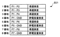
図6は、検査順序記憶部85に記憶された検査箇所データの一例である検査順序テーブル851を示す図である。図6に示す検査順序テーブル851において、「P1−P2」、「P1−P3」、「P1−P4」は、それぞれ検査順序テーブル851の1番地、2番地、3番地に、「導通検査」と関連付けて記憶されている。
【0033】
次に、ステップS104において、並替え処理部84によって、検査箇所データ記憶部83に記憶されている容量検査点テーブル832から、変数Head(i)すなわち”P1”と等しいヘッドを含む検査箇所データである「P1−GND」が抽出され、静電容量検査のための検査箇所データとして検査順序テーブル851の4番地に、「静電容量検査」と関連付けて記憶される。
【0034】
そして、ヘッドテーブル833のアドレスを示す変数iに1が加算され(ステップS105)、ヘッドテーブル833のi番地にデータが記憶されているか否かが確認され、i番地にデータが記憶されていないとき(ステップS106でYES)、すべての検査箇所データに対して並び替え処理が終了したと判断して図4に示すステップS2へ移行する一方、i番地にヘッドデータが記憶されているとき(ステップS106でNO)、検査箇所データの並び替え処理を継続すべく再びステップS102へ移行する。
【0035】
以上、ステップS102〜S106を繰り返すことにより、並替え処理部84によって、検査順序テーブル851の5番地に検査箇所データ「P5−P6」が「導通検査」と関連付けて記憶され、6番地に検査箇所データ「P5−GND」が「静電容量検査」と関連付けて記憶され、7番地に検査箇所データ「P7−P8」が「導通検査」と関連付けて記憶され、8番地に検査箇所データ「P7−GND」が「静電容量検査」と関連付けて記憶される。そして、並替え処理部84によって、すべての検査箇所データに対して並び替え処理が終了したと判断されることにより図4に示すステップS2へ移行する。
【0036】
次に、ステップS2において、検査制御部8によって、検査順序記憶部85に記憶されている検査順序テーブル851のアドレスを示す変数jが1に初期化される。そして、検査制御部8によって、検査順序テーブル851のj番地に記憶されている検査箇所データの検査の種類が確認される(ステップS3)。そして、今、検査順序テーブル851の1番地に記憶されている検査箇所データは「導通検査」と関連付けられているので、導通検査を行うべくステップS4へ移行する。
【0037】
次に、ステップS4において、検査順序テーブル851の1番地に記憶されている検査箇所データ「P1−P2」に基いて、基板データ記憶部81に記憶されている座標データやネットデータに基づき検査制御部8から出力された制御信号に応じて、位置決め制御部6,7によりプローブ2,3がX軸、Y軸及びZ軸方向に移動制御されると共にそれぞれ基板100上の検査点に接触され、その2検査点の間の抵抗値が抵抗値検出部4によって測定される。この場合、プローブ2がパッドP1へ、プローブ3がパッドP2へ、各プローブの移動がそれぞれ1回づつ、計2回行われる。
【0038】
具体的には、例えば、まず検査箇所データ「P1−P2」に基づいて、検査制御部8からの制御信号に応じてパッドP1とパッドP2とにそれぞれプローブ2,3が移動されると共に接触され、抵抗値検出部4によってプローブ2,3間の抵抗値が測定され、その抵抗測定値が検査制御部8によって所定の導通判定用基準値と比較される。そして、検査制御部8によって、その抵抗測定値が導通判定用基準値よりも小さいとき(ステップS5でYES)、パッドP1とパッドP2との間の導通状態は良好であると判定されてステップS6へ移行する一方、その抵抗測定値が導通判定用基準値を越えているとき(ステップS5でNO)、パッドP1とパッドP2との間の導通状態は不良であると判定されてステップS11へ移行し、基板100は不良であると判定されると共に、検査制御部8からの制御信号に応じて操作表示部9に検査結果が不良である旨の表示が行われる。
【0039】
次に、検査順序テーブル851のアドレスを示す変数jに1が加算され(ステップS6)、検査順序テーブル851のj番地に検査箇所データが記憶されているか否かが確認され、j番地に検査箇所データが記憶されていないとき(ステップS7でYES)、すべての検査箇所データに対して検査が終了したので良判定すべくステップS10へ移行する一方、j番地に検査箇所データが記憶されているとき(ステップS7でNO)、検査を継続すべく再びステップS3へ移行する。
【0040】
以上、ステップS3〜S7の処理が、検査順序テーブル851の2番地、3番地に記憶されている検査箇所データ「P1−P3」「P1−P4」について繰り返される。この場合、プローブ2は、パッドP1に接触させたまま、プローブ3をパッドP3,P4に接触させるべく計2回移動が行われる。
【0041】
次に、ステップS3において、検査順序テーブル851の4番地の検査箇所データの検査の種類が確認され、「P1−GND」が「静電容量検査」と関連付けて記憶されているので、静電容量検査を行うべくステップS8へ移行する。
【0042】
次に、ステップS8において、検査順序テーブル851の4番地に記憶されている検査箇所データ「P1−GND」に基いて、静電容量検出部5によって、プローブ2とクリップ10との間の静電容量が測定される。この場合、プローブ2は既にパッドP1に接触されているので、プローブ2を移動させる必要がない。
【0043】
そして、静電容量検出部5によって測定された静電容量測定値が検査制御部8によって基準容量データ記憶部82に記憶されている配線パターンN1の良否判定用静電容量データと比較される(ステップS9)。
【0044】
そして、検査制御部8によって、その静電容量測定値が良否判定用静電容量データで示される静電容量の範囲に入っていると判断されたとき(ステップS9でYES)配線パターンN1と他の配線パターンとの間には短絡不良が無いと判定されてステップS6へ移行する一方、その静電容量測定値が良否判定用静電容量データで示される静電容量の範囲に入っていないと判断されたとき(ステップS9でNO)、配線パターンN1と他の配線パターンとの間に短絡不良が有ると判定されてステップS11へ移行し、基板100は不良であると判定されると共に、検査制御部8からの制御信号に応じて操作表示部9に検査結果が不良である旨の表示が行われる。
【0045】
以上、ステップS3〜S9の処理が、検査順序テーブル851の5,6,7,8番地に記憶されている検査箇所データ「P5−P6」(導通検査)、「P5−GND」(静電容量検査)、「P7−P8」(導通検査)、「P7−GND」(静電容量検査)に基いて繰り返される。この場合、プローブ2の移動回数は2回、プローブ3の移動回数は2回、計4回となる。
【0046】
そして、ステップS7において、検査順序テーブル851のj番地に検査箇所データが記憶されていないことが確認されると(ステップS7でYES)、すべての検査箇所データに対して検査が終了し、ステップS10へ移行して基板100は良品であると判定すると共に、検査制御部8からの制御信号に応じて操作表示部9に検査結果が良である旨の表示が行われる。そして、基板100の検査を終了する。
【0047】
以上、ステップS1〜S11の処理により、基板100の検査がすべて終了する。そして、プローブ2,3の移動回数は、合計2+2+4=8回となる。以上のように、ステップS1の処理を行わない従来の基板検査方法の場合のプローブの移動回数11回よりも、プローブの移動回数を低減することができる。
【0048】
なお、基板100に対して、導通検査と静電容量検査の2種類の検査を行う例を示したが、例えば検査対象となる配線パターンと他の配線パターンとの間の抵抗値を測定することにより、検査対象配線パターンと他の配線パターンとの間の短絡不良が無いことを検査する絶縁検査や、導通検査時にプローブ間の抵抗が所定値以下かどうかを判定する抵抗値検査、その他の種類の検査と組み合わせて実行されるものであっても良い。検査の種類が増加した場合、さらにプローブの移動回数の低減が期待できる。上記絶縁検査は、例えば、ベタ導体が全ての配線パターンをカバーしていないときに、カバーされていない配線パターンと他の配線パターンとの間の短絡の有無の検出に有効である。このように、ベタ導体は、必ずしも全ての配線パターンをカバーしていなくとも、複数の配線パターンをカバーしていれば、静電容量測定による短絡検査の効果が得られる。
【0049】
また、配線パターンN1の検査を行うとき、「P1−P2」、「P1−P3」、「P1−P4」、「P1−GND」の順序で検査を行う例を示したが、例えば、「P1−P2」、「P1−GND」、「P1−P3」、「P1−P4」の順序で検査を行ったり、「P1−P2」、「P1−P3」、「P1−GND」、「P1−P4」の順序で検査を行ったりする構成としてもよい。例えば、「P1−P2」、「P1−GND」、「P1−P3」、「P1−P4」の順序で検査を行う場合には、「P1−P2」の検査後、「P1−P3」の検査を行うためにプローブ3を、パッドP2からパッドP3へ移動させる移動時間の間に、導体パターン105に接続されているクリップ10と、パッドP1にさせた状態のままのパッドP1とを用いて平行して静電容量検査を実行することができるので、さらに検査時間を低減することができる。
【0050】
また、導体パターン105に接続されたクリップ10を用いる例を示したが、クリップ10を用いず、代わりにプローブ3を移動させ、導体パターン105に接触させて用いる構成としても良い。この場合、図1において、クリップ10の代わりにプローブ3が静電容量検出部5に接続される。
【0051】
更に、上記実施例においては、検査順序の並べ替えを行っていたが、配線パターンの配置が予め決められた基板を大量に検査する場合には、その基板についての検査順序を本発明に従ったものに予め設定し、その設定された検査順序を記憶しておき、その記憶値に基づいてプローブの移動を制御するようにしてもよい。
【0052】
【発明の効果】
請求項1及び4に記載の発明によれば、各配線パターンについて、当該配線パターンの代表検査点に検査用接触子の一方を位置させた状態で、複数種類の検査が行われるので、検査用接触子の移動回数が減少する結果、複数の種類の検査を行うときの検査工数を低減することができる。
【0053】
請求項2に記載の発明によれば、複数の配線パターンをカバーする導電面と代表検査点に一つの接触子が位置している配線パターンとの間の静電容量から配線パターン間の短絡の有無を検査することにより短絡検査の工数が削減される上に、検査用接触子の移動回数減少による工数減少が加わり、より効率的な検査が行える。
【0054】
請求項3に記載の発明によれば、共通検査点に位置させた検査用接触子と代表検査点に位置させた検査用接触子とを用いた検査と、第三の検査用接触子の移動を平行して行うことができるので、検査工数を低減することができる。
【図面の簡単な説明】
【図1】本発明の一実施形態に係る基板検査装置の構成の一例を説明するための図である。
【図2】検査対象の基板の一例を示す図である。
【図3】検査箇所データ記憶部に記憶されている検査箇所データ及びヘッドデータの一例を示す図である。
【図4】図1に示す基板検査装置の動作の一例を示すフローチャートである。
【図5】並替え処理部の動作の一例を示すフローチャートである。
【図6】検査順序記憶部に記憶された検査箇所データの一例を示す図である。
【符号の説明】
1 基板検査装置
2,3 プローブ(検査用接触子)
4 抵抗値検出部
5 静電容量検出部
6,7 位置決め制御部
8 検査制御部
9 操作表示部
10 クリップ(検査用接触子)
81 基板データ記憶部
82 基準容量データ記憶部
83 検査箇所データ記憶部
84 並替え処理部
85 検査順序記憶部
100 基板
105 導体パターン(共通検査点)
831 導通検査点テーブル
832 容量検査点テーブル
833 ヘッドテーブル(代表検査点記憶部)
851 検査順序テーブル
N1,N2,N3 配線パターン
P1,P5,P7 パッド(代表検査点)
P2,P3,P4,P6,P8 パッド(検査点)[0001]
BACKGROUND OF THE INVENTION
The present invention relates to an inspection apparatus that performs a plurality of inspections such as a so-called wiring continuity and a short-circuiting inspecting whether there is a disconnection in a wiring of a substrate such as a printed wiring board or whether there is a short circuit between wiring patterns. The present invention is not limited to a printed wiring board, but is applicable to inspection of electrical wiring on various substrates such as flexible substrates, multilayer wiring substrates, electrode plates for liquid crystal displays and plasma displays, and film carriers for semiconductor packages. In this specification, these various wiring boards are collectively referred to as “substrates”.
[0002]
[Prior art]
Conventionally, wiring formed on a substrate such as a printed circuit board or a package substrate used for an IC package, connection wiring such as a through hole or via, and a land or pad for connecting an IC package or a semiconductor chip to the
[0003]
In such a substrate inspection apparatus using a pair of inspection contacts, in order to perform inspection efficiently, the pair of inspection contacts are sequentially brought into contact with inspection points on the wiring, and the inspection target wiring between the contacts is arranged. After or before conducting a continuity test to check that the wiring pattern is conductive based on the resistance value, it was formed in a planar shape for the purpose of supplying power and ground to almost the entire substrate A wiring pattern to be inspected and other wiring patterns based on the capacitance between the conductive reference plane and the wiring pattern to be inspected provided to cover all the wiring patterns of the board separately from the solid conductor portion or the board There has been proposed an inspection apparatus capable of performing a plurality of types of inspection, such as a capacitance inspection for inspecting that there is no short circuit between them (for example, see Patent Document 1).
[0004]
[Patent Document 1]
Japanese Patent Publication No. 4-17394
[0005]
[Problems to be solved by the invention]
However, in the conventional inspection apparatus, the movement of each inspection contact in the short circuit inspection is greatly reduced by inspecting the presence or absence of a short circuit between the wiring patterns using the solid conductor or the conductive reference surface. However, the number of times of moving each inspection contact to the position of the inspection point in order to perform the inspection is quite large. In addition, since the operation for moving the inspection contact to the position of the inspection point takes time, there is a disadvantage that the number of inspection steps for the substrate increases if the number of movements of the inspection contact is large.
[0006]
The present invention has been made in view of the above circumstances, and an object of the present invention is to provide a substrate inspection apparatus that reduces the number of times the inspection contact is moved when performing a plurality of types of inspections and reduces the number of inspection steps.
[0007]
[Means for Solving the Problems]
According to the first aspect of the present invention, the presence / absence of disconnection of the wiring on the substrate and the wiring pattern using at least two movable inspection contacts in a predetermined order with respect to the plurality of wiring patterns formed on the substrate A board inspection method for performing a plurality of types of inspection such as the presence or absence of a short circuit between one of the inspection points set to inspect each of the wiring patterns as a representative inspection point, and for each of the wiring patterns The plurality of types of inspections are performed with one of the inspection contacts positioned at the representative inspection point. According to the first aspect of the present invention, for each wiring pattern, a plurality of types of inspections are performed with one of the inspection contacts positioned at the representative inspection point of the wiring pattern.
[0008]
According to a second aspect of the present invention, in the substrate inspection method according to the first aspect of the present invention, another inspection contact is started with one of the inspection contacts positioned at the representative inspection point. The wiring pattern is sequentially positioned at inspection points other than the representative inspection point to inspect for the presence or absence of disconnection in the wiring, and one contact is located on the conductive surface covering the plurality of wiring patterns and the representative inspection point. It is characterized by inspecting the presence or absence of a short circuit between the wiring patterns from the capacitance between the wiring patterns. According to the invention described in
[0009]
According to a third aspect of the present invention, in the substrate inspection method according to the second aspect, the inspection contact located at the representative inspection point and the conductive surface are electrically connected while the other inspection contact is moved. The presence or absence of the short circuit is inspected by using a contact point connected in a regular manner. According to the third aspect of the invention, since the inspection for the presence or absence of a short circuit is performed while the other inspection contact is moved, the number of inspection steps is further reduced.
[0010]
The invention according to claim 4 is a substrate that performs a plurality of types of inspections such as the presence or absence of disconnection of the wiring in the substrate and the presence or absence of a short circuit between the wiring patterns in a predetermined order with respect to the plurality of wiring patterns formed on the substrate. A representative inspection point memory that stores at least two movable inspection contacts and a representative inspection point that is one of inspection points set to inspect each of the wiring patterns. And an inspection operation control unit that performs the plurality of types of inspection in a state where one of the inspection contacts is positioned at the representative inspection point for each of the wiring patterns. According to the invention described in claim 4, for each wiring pattern, a plurality of types of inspections are performed in a state where one of the inspection contacts is positioned at a representative inspection point of the wiring pattern.
[0011]
DETAILED DESCRIPTION OF THE INVENTION
Embodiments according to the present invention will be described below with reference to the drawings. FIG. 1 is a diagram for explaining an example of the configuration of a
[0012]
FIG. 2 is a front view of the
[0013]
The
[0014]
The resistance value detection unit 4 measures the resistance value between the
[0015]
The
[0016]
The
[0017]
Then, the
[0018]
The board
[0019]
The reference capacitance data storage unit 82 stores capacitance data serving as a reference for performing pass / fail judgment of a wiring pattern or the like to be inspected from the capacitance measured by the
[0020]
The inspection location data storage unit 83 stores inspection location data indicating inspection points for performing the continuity inspection and the capacitance inspection for each type of inspection. The inspection location data storage unit 83 stores one of the pads included in each wiring pattern as a head (representative inspection point) and stores data indicating the head as head data.
[0021]
FIG. 3 is a diagram illustrating an example of inspection location data and head data stored in the inspection location data storage unit 83. FIG. 3A shows a continuity test point table 831 which is an example of a data table showing test locations for conducting the continuity test. For example, “P1-P2” indicates that the
[0022]
FIG. 3B shows a capacitance inspection point table 832 which is an example of a data table indicating inspection locations for performing capacitance inspection. For example, “P1-GND” indicates that the
[0023]
FIG. 3C shows a head table 833 which is an example of a data table indicating head data. The head data “P1” of the wiring pattern N1 is assigned to address 1, and the head data of the wiring pattern N2 is used as the head data. A certain “P5” is stored in the second address, and “P7” which is the head data of the wiring pattern N3 is stored in the third address.
[0024]
The inspection
[0025]
Next, the operation of the
[0026]
At this time, according to the conventional inspection method, when conducting the continuity inspection and the capacitance inspection using the inspection location data stored in the continuity inspection point table 831 and the capacitance inspection point table 832, first, the continuity inspection point. Based on the inspection location data “P1-P2” stored in the table 831, the
[0027]
Further, the
[0028]
Therefore, in this embodiment, in order to reduce the number of inspection steps for the
[0029]
In step S <b> 1, the
[0030]
First, the
[0031]
Next, in step S103, the
[0032]
FIG. 6 is a diagram illustrating an inspection order table 851 that is an example of inspection location data stored in the inspection
[0033]
Next, in step S104, the
[0034]
Then, 1 is added to the variable i indicating the address of the head table 833 (step S105), and it is confirmed whether or not data is stored in the i address of the head table 833, and no data is stored in the i address. (YES in step S106), it is determined that the rearrangement process has been completed for all the inspection point data, and the process proceeds to step S2 shown in FIG. 4, while the head data is stored at address i (step S106). NO), the process proceeds to step S102 again to continue the rearrangement process of the inspection location data.
[0035]
As described above, by repeating steps S102 to S106, the
[0036]
Next, in step S <b> 2, the
[0037]
Next, in step S4, based on the inspection location data “P1-P2” stored at
[0038]
Specifically, for example, based on the inspection location data “P1-P2”, the
[0039]
Next, 1 is added to the variable j indicating the address of the inspection sequence table 851 (step S6), and it is confirmed whether or not the inspection location data is stored at the j-th address of the inspection sequence table 851. When data is not stored (YES in step S7), inspection has been completed for all inspection point data, so that the process proceeds to step S10 to make a good determination, while inspection point data is stored at address j. (NO in step S7), the process proceeds to step S3 again to continue the inspection.
[0040]
The processes in steps S3 to S7 are repeated for the inspection location data “P1-P3” and “P1-P4” stored at the second address and the third address in the inspection order table 851. In this case, the
[0041]
Next, in step S3, the inspection type of the inspection location data at address 4 in the inspection order table 851 is confirmed, and “P1-GND” is stored in association with “electrostatic capacitance inspection”. The process proceeds to step S8 to perform inspection.
[0042]
Next, in step S <b> 8, electrostatic capacitance between the
[0043]
Then, the capacitance measurement value measured by the
[0044]
When the
[0045]
As described above, the processes in steps S3 to S9 are the inspection location data “P5-P6” (continuity inspection) and “P5-GND” (capacitance) stored at
[0046]
If it is confirmed in step S7 that no inspection location data is stored at address j in the inspection order table 851 (YES in step S7), the inspection is completed for all inspection location data, and step S10 is completed. Then, it is determined that the
[0047]
As described above, the inspection of the
[0048]
In addition, although the example which performs 2 types of test | inspection with respect to the board |
[0049]
Further, when the wiring pattern N1 is inspected, the example in which the inspection is performed in the order of “P1-P2”, “P1-P3”, “P1-P4”, “P1-GND” has been shown. -P2 ”,“ P1-GND ”,“ P1-P3 ”,“ P1-P4 ”in order, or“ P1-P2 ”,“ P1-P3 ”,“ P1-GND ”,“ P1- The inspection may be performed in the order of “P4”. For example, when the inspection is performed in the order of “P1-P2”, “P1-GND”, “P1-P3”, “P1-P4”, the inspection of “P1-P3” is performed after the inspection of “P1-P2”. During the movement time for moving the
[0050]
Moreover, although the example using the
[0051]
Further, in the above embodiment, the inspection order is rearranged. However, when a large number of substrates with predetermined wiring pattern arrangements are inspected, the inspection order for the substrates is in accordance with the present invention. It may be set in advance, the set inspection order is stored, and the movement of the probe may be controlled based on the stored value.
[0052]
【The invention's effect】
According to the first and fourth aspects of the invention, for each wiring pattern, a plurality of types of inspection are performed with one of the inspection contacts positioned at the representative inspection point of the wiring pattern. As a result of the reduction in the number of times the contact is moved, the number of inspection steps when performing a plurality of types of inspection can be reduced.
[0053]
According to the second aspect of the present invention, the short circuit between the wiring patterns can be caused by the capacitance between the conductive surface covering the plurality of wiring patterns and the wiring pattern in which one contactor is located at the representative inspection point. Inspecting the presence or absence reduces the number of man-hours for short-circuit inspection, and also reduces the number of man-hours due to a decrease in the number of times the inspection contact is moved, thereby enabling more efficient inspection.
[0054]
According to the invention of
[Brief description of the drawings]
FIG. 1 is a diagram for explaining an example of a configuration of a substrate inspection apparatus according to an embodiment of the present invention.
FIG. 2 is a diagram showing an example of a substrate to be inspected.
FIG. 3 is a diagram illustrating an example of inspection location data and head data stored in an inspection location data storage unit;
4 is a flowchart showing an example of the operation of the substrate inspection apparatus shown in FIG.
FIG. 5 is a flowchart illustrating an example of an operation of a rearrangement processing unit.
FIG. 6 is a diagram illustrating an example of inspection location data stored in an inspection order storage unit.
[Explanation of symbols]
1 Board inspection equipment
2, 3 probe (contact for inspection)
4 Resistance value detector
5 Capacitance detector
6,7 Positioning controller
8 Inspection control unit
9 Operation display
10 clips (contact for inspection)
81 Substrate data storage unit
82 Reference capacity data storage unit
83 Inspection location data storage
84 Rearrangement processing part
85 Inspection sequence storage
100 substrates
105 Conductor pattern (common inspection point)
831 Continuity test point table
832 Capacity inspection point table
833 Head Table (Representative Inspection Point Storage Unit)
851 Inspection sequence table
N1, N2, N3 wiring pattern
P1, P5, P7 pads (representative inspection points)
P2, P3, P4, P6, P8 pad (inspection point)
Claims (4)
Priority Applications (1)
| Application Number | Priority Date | Filing Date | Title |
|---|---|---|---|
| JP2003185532A JP2005017221A (en) | 2003-06-27 | 2003-06-27 | Substrate inspecting method and device therefor |
Applications Claiming Priority (1)
| Application Number | Priority Date | Filing Date | Title |
|---|---|---|---|
| JP2003185532A JP2005017221A (en) | 2003-06-27 | 2003-06-27 | Substrate inspecting method and device therefor |
Publications (1)
| Publication Number | Publication Date |
|---|---|
| JP2005017221A true JP2005017221A (en) | 2005-01-20 |
Family
ID=34184956
Family Applications (1)
| Application Number | Title | Priority Date | Filing Date |
|---|---|---|---|
| JP2003185532A Pending JP2005017221A (en) | 2003-06-27 | 2003-06-27 | Substrate inspecting method and device therefor |
Country Status (1)
| Country | Link |
|---|---|
| JP (1) | JP2005017221A (en) |
Cited By (6)
| Publication number | Priority date | Publication date | Assignee | Title |
|---|---|---|---|---|
| JP2009109445A (en) * | 2007-11-01 | 2009-05-21 | Hioki Ee Corp | Circuit board inspection equipment |
| JP2010175489A (en) * | 2009-02-02 | 2010-08-12 | Hioki Ee Corp | Circuit board inspecting apparatus and circuit board inspecting method |
| CN102116817B (en) * | 2009-12-31 | 2013-05-29 | 德律科技股份有限公司 | Electrical connection defect detection device |
| JP2014102187A (en) * | 2012-11-21 | 2014-06-05 | Hioki Ee Corp | Circuit board inspection device and circuit board inspection method |
| JP2017020965A (en) * | 2015-07-14 | 2017-01-26 | 株式会社日本マイクロニクス | Electrical connection device and inspection method |
| JP2020098147A (en) * | 2018-12-18 | 2020-06-25 | 日置電機株式会社 | Circuit board inspection apparatus, control method thereof, and program |
-
2003
- 2003-06-27 JP JP2003185532A patent/JP2005017221A/en active Pending
Cited By (7)
| Publication number | Priority date | Publication date | Assignee | Title |
|---|---|---|---|---|
| JP2009109445A (en) * | 2007-11-01 | 2009-05-21 | Hioki Ee Corp | Circuit board inspection equipment |
| JP2010175489A (en) * | 2009-02-02 | 2010-08-12 | Hioki Ee Corp | Circuit board inspecting apparatus and circuit board inspecting method |
| CN102116817B (en) * | 2009-12-31 | 2013-05-29 | 德律科技股份有限公司 | Electrical connection defect detection device |
| JP2014102187A (en) * | 2012-11-21 | 2014-06-05 | Hioki Ee Corp | Circuit board inspection device and circuit board inspection method |
| JP2017020965A (en) * | 2015-07-14 | 2017-01-26 | 株式会社日本マイクロニクス | Electrical connection device and inspection method |
| JP2020098147A (en) * | 2018-12-18 | 2020-06-25 | 日置電機株式会社 | Circuit board inspection apparatus, control method thereof, and program |
| JP7245042B2 (en) | 2018-12-18 | 2023-03-23 | 日置電機株式会社 | Circuit board inspection equipment |
Similar Documents
| Publication | Publication Date | Title |
|---|---|---|
| JP7105977B2 (en) | Inspection system and failure analysis/prediction method for inspection system | |
| JP3558434B2 (en) | Electrical wiring inspection method and apparatus | |
| KR20090027610A (en) | Board inspection apparatus and board inspection method | |
| KR20080044785A (en) | Insulation inspection device and insulation inspection method | |
| JP2005017221A (en) | Substrate inspecting method and device therefor | |
| JP5004010B2 (en) | Substrate inspection apparatus and substrate inspection method | |
| JP4264305B2 (en) | Substrate inspection apparatus and substrate inspection method | |
| JP2005069864A (en) | Apparatus, system, method, program and auxiliary means for inspecting substrate | |
| JP2019060627A (en) | Substrate inspection apparatus and substrate inspection method | |
| JP2001235505A (en) | Circuit board inspection equipment | |
| JPH09230005A (en) | Circuit board inspection equipment | |
| JP2005315775A (en) | Four-terminal inspection method and single-terminal inspection jig using a single-sided moving probe | |
| WO2007138831A1 (en) | Board examination method and board examination device | |
| JP2009288115A (en) | Inspection device and inspection method | |
| JP3784479B2 (en) | Circuit board inspection method | |
| JP2004361249A (en) | Substrate inspection device | |
| JP5420303B2 (en) | Circuit board inspection apparatus and circuit board inspection method | |
| KR20140009027A (en) | Apparatus and method for inspecting board | |
| JP2010014597A (en) | Mobile contact inspection apparatus | |
| JP3276755B2 (en) | Detecting soldering failure of leads on mounted components | |
| JP4369002B2 (en) | Circuit board inspection equipment | |
| JP7704360B2 (en) | Inspection device and inspection method | |
| JP2007286004A (en) | Substrate inspection apparatus and substrate inspection method | |
| JP2020128881A (en) | Short circuit inspection system, and short circuit inspection method | |
| JP6733199B2 (en) | Inspection device, inspection method, and inspection program |
Legal Events
| Date | Code | Title | Description |
|---|---|---|---|
| A621 | Written request for application examination |
Free format text: JAPANESE INTERMEDIATE CODE: A621 Effective date: 20060621 |
|
| A977 | Report on retrieval |
Free format text: JAPANESE INTERMEDIATE CODE: A971007 Effective date: 20080421 |
|
| A131 | Notification of reasons for refusal |
Free format text: JAPANESE INTERMEDIATE CODE: A131 Effective date: 20080501 |
|
| A02 | Decision of refusal |
Free format text: JAPANESE INTERMEDIATE CODE: A02 Effective date: 20080902 |