EP3803972B1 - Die stacking for multi-tier 3d integration - Google Patents
Die stacking for multi-tier 3d integration Download PDFInfo
- Publication number
- EP3803972B1 EP3803972B1 EP19810608.0A EP19810608A EP3803972B1 EP 3803972 B1 EP3803972 B1 EP 3803972B1 EP 19810608 A EP19810608 A EP 19810608A EP 3803972 B1 EP3803972 B1 EP 3803972B1
- Authority
- EP
- European Patent Office
- Prior art keywords
- semiconductor die
- die
- semiconductor
- wafer
- stack
- Prior art date
- Legal status (The legal status is an assumption and is not a legal conclusion. Google has not performed a legal analysis and makes no representation as to the accuracy of the status listed.)
- Active
Links
Images


Classifications
-
- H10W99/00—
-
- H10W20/42—
-
- H10P54/00—
-
- H10P72/74—
-
- H10W20/023—
-
- H10W20/0245—
-
- H10W70/635—
-
- H10W72/0198—
-
- H10W72/30—
-
- H10W72/851—
-
- H10W72/90—
-
- H10W80/00—
-
- H10W90/00—
-
- H10P72/7424—
-
- H10P72/743—
-
- H10W72/07207—
-
- H10W72/07331—
-
- H10W72/244—
-
- H10W72/252—
-
- H10W72/353—
-
- H10W72/952—
-
- H10W74/00—
-
- H10W74/15—
-
- H10W76/10—
-
- H10W80/312—
-
- H10W80/327—
-
- H10W90/20—
-
- H10W90/28—
-
- H10W90/288—
-
- H10W90/291—
-
- H10W90/297—
-
- H10W90/722—
-
- H10W90/724—
-
- H10W90/732—
-
- H10W90/734—
-
- H10W90/792—
Definitions
- One frequently-used package consists of a substrate upon which a die is mounted.
- the upper surface of the substrate includes electrical interconnects.
- the die is manufactured with a plurality of bond pads.
- a collection of solder joints are provided between the bond pads of the die and the substrate interconnects to establish ohmic contact.
- a lid is attached to the substrate to cover the die.
- the lid serves as both a protective cover and a heat transfer pathway.
- Stacked dies arrangements involve placing or stacking one or more semiconductor dies on a base semiconductor chip.
- the base semiconductor die is a high heat dissipating device, such as a microprocessor.
- the stacked dies are sometimes memory devices. In a typical conventional manufacturing process the dies are stacked one at a time on the base die. Die-to-die electrical connections are by way of bumps and through-chip-vias.
- US 2017/250172 discloses a semiconductor device and a method of stacking semiconductor die with protection circuits and interconnect structures to increase ESD current discharge capability. More precisely, said document shows a method of manufacturing a semiconductor die device, comprising:
- a conventional die stacking technique stacks dies sequentially, one die on top of the first die and so on up to the top die of the stack.
- TDVs through-die-vias
- a reveal process is necessary to reveal the TDVs of one die before the next die is mounted. This is typically done in one conventional process by creating a reconstituted wafer of previously singulated dies and then performing the reveal process on the reconstituted wafer. Often times a gap filling process is necessary to avoid adversely affecting the lower dies in the stack during reveal of the TDVs of the current topmost die in the stack.
- the techniques disclosed herein enable the creation of die stacks where TDV reveals can always be performed at the wafer level without the need to resort to reconstitution. Gap filling processes during stack creation are not necessary.
- FIG. 1 is a sectional view of an exemplary semiconductor die device 10 that includes a stack 15 of multiple semiconductor dies mounted on another semiconductor die 20.
- the semiconductor die device 10 can be mounted on a circuit board (not shown), such as a package substrates, a system board, a daughter board, a circuit cards or other.
- the stack 15 in this illustrative arrangement consists of four semiconductor dies 25, 30, 35 and 40, but of course, other numbers are possible.
- the semiconductor dies 20, 25, 30, 35 and 40 include respective back end of line structures (BEOL) 45, 50, 55, 60 and 65.
- BEOL back end of line structures
- the BEOLs 45, 50, 55, 60 and 65 consist of strata of logic and other devices that make up the functionalities of the semiconductor dies 20, 25, 30, 35 and 40 as well as plural metallization and interlevel dielectric layers.
- the semiconductor dies 25, 30, 35 and 40 of the semiconductor die stack 15 can have different footprints or approximately the same footprint. In the illustrated arrangement, the semiconductor dies 25, 30, 35 and 40 of the semiconductor die stack 15 can have successively smaller footprints, that is, the semiconductor die 40 is smaller than the semiconductor die 35, which in-turn is smaller than the semiconductor die 30 and so on.
- Insulating layers 90, 95, 100 and 105 are positioned between the semiconductor die 25 and semiconductor die 20, the semiconductor die 30 and the semiconductor die 25, the semiconductor die 35 and the semiconductor die 30 and the semiconductor die 40 and the semiconductor die 35 respectively.
- the insulating layers 90, 95, 100 and 105 can be unitary or multiple layer structures as described in more detail below.
- interconnects 70, 75, 80 and 85 can be hybrid bonds, conductive pillars, solder bumps, solder micro bumps or other types of interconnects.
- insulating layer 100 and interconnects 80 between semiconductor dies 35 and 30 are such that mounting the first semiconductor die on the second semiconductor die includes forming a first insulating bonding layer 100 having a first glass layer and a second glass layer between and bonding the first semiconductor die and the second semiconductor die and annealing to bond the first glass layer to the second glass layer and to metallurgically bond conductor structures of the first semiconductor die and conductor structures of the second semiconductor die.
- the semiconductor dies 20, 25, 30, 35 and 40 can be any of a variety of integrated circuits.
- processors such as microprocessors, graphics processing units, accelerated processing units that combine aspects of both, memory devices, an application integrated specific circuit or other.
- the semiconductor die 20 can be a processor and the semiconductor dies 25, 30, 35 and 40 can be memory dies, such as DRAM, SRAM or other.
- dummy components 110 and 115 are mounted on the semiconductor die 20 and secured thereto by way of adhesive layers 120 and 125, respectively.
- the dummy components 110 and 115 can be composed of silicon, germanium, or other type of semiconductor or even a dielectric material and serves as a heat transfer avenue for conducting heat away from the semiconductor die 20 and other components of the semiconductor die device 10.
- the adhesive layers 120 and 125 can be various types of organic adhesives, inorganic bonding layers, glass-based adhesives or even solder materials in other arrangements.
- a non-exhaustive list includes epoxies, an organic TIM, such as silicone rubber mixed with aluminum particles and zinc oxide.
- Compliant base materials other than silicone rubber and thermally conductive particles other than aluminum may be used.
- Thermal greases and gold, platinum and silver represent a few examples.
- the adhesive layers 120 and 125 can be nanofoils composed of layers of aluminum and nickel.
- a molding material 130 at least laterally encases the semiconductor die stack 15 and is positioned between the semiconductor die stack 15 and the dummy components 110 and 115.
- the materials for the molding material 130 can have a molding temperature of about 165 °C.
- Two commercial variants are Sumitomo EME-G750 and G760.
- Well-known compression molding techniques can be used to mold the molding material 130.
- TDV Through die electrical conductivity is provided by plural through-die-vias
- the semiconductor die 20 includes plural TDVs 135 that are connected to the interconnects 70 and to I/Os 140.
- the TDVs 135 (and any related disclosed conductors, such as pillars and pads) can be composed of various conductor materials, such as copper, aluminum, silver, gold, platinum, palladium or others.
- each TDV 135 is surrounded laterally by a liner layer (not shown) of SiOx or other insulator and a barrier layer of TiN or other barrier materials.
- the semiconductor die 25 similarly includes TDVs 145 that are connected between the interconnects 70 and 75.
- the semiconductor die 30 includes TDVs 150 that connect between the interconnects 75 and 80 and the semiconductor die 35 includes TDVs 155 that connect between the interconnects 80 and 85.
- the semiconductor die 40 includes plural TDVs 160, which in this illustrative arrangement are not revealed, but of course could be revealed using the thinning/reveal processes disclosed herein to facilitate interconnection with yet another die stacked on top of the stack 15 if desired.
- the I/Os 140 enable the semiconductor die device 10 to interface electrically with another component such as a circuit board or other device, and can be solder bumps, balls or other types of interconnect structures.
- Well-known lead free solders, such as Sn-Ag, Sn-Ag-Cu or others can be used for the I/Os 140 and other solder structures disclosed herein.
- each of the interconnects 75 consists of a bumpless oxide hybrid bond.
- the interconnect 75 between the semiconductor die 25 and the BEOL 55 of the semiconductor die 30 is made up of a metallurgical bond between a bond pad 170 of the BEOL 55 and a bond pad 172 of the semiconductor die 25.
- the bond pad 170 is connected to the TDV 150 and the bond pad 172 is connected to the TDV 145.
- the insulating structure 95 joins the semiconductor die 25 to the semiconductor die 30 and consists of a glass layer 175, such as SiOx, of the semiconductor die 30 and another glass layer 180, such as silicon oxynitride, of the semiconductor die 25.
- the glass layers 175 and 180 are preferably deposited on the semiconductor dies 25 and 30, respectively, by plasma enhanced chemical vapor deposition (PECVD).
- PECVD plasma enhanced chemical vapor deposition
- the bond pad 170 is positioned in the glass layer 175 and the bond pad 172 is positioned in the glass layer 180.
- the bond pad 170 and the bond pad 172 are metallurgically bonded by way of an anneal process.
- the semiconductor die 30 is brought down or otherwise positioned on the semiconductor die 25 so that the glass layer 175 is on or in very close proximity to the glass layer 180 and the bond pad 170 is on or in very close proximity to the bond pad 172. Thereafter, an anneal process is performed, which produces a transitory thermal expansion of the bond pads 170 and 172 bringing those structures into physical contact and causing them to form a metallurgical bond that persists even after the semiconductor dies 25 and 30 are cooled and the bond pads 170 and 172 contract thermally. Copper performs well in this metal bonding process, but other conductors could be used. There is also formed an oxide/oxynitride bond between the glass layer 175 and the glass layer 180.
- An exemplary anneal is performed at about 300° C for about 30 to 60 minutes to form the requisite oxynitride-oxide bonds and metal-metal bonds.
- conductive pillars on each of two adjacent stacked dies can be thermal compression bonded.
- direction oxide bond and TSV last connection can be used. In this technique, facing sides of each two adjacent stacked dies each receive an oxide film. The oxide films are subsequently planarized using chemical mechanical polishing and then plasma treated to become hydrophillic. The oxide surfaces are next placed together and annealed to form a bond.
- FIG. 3 is a sectional view of a portion of a semiconductor wafer 185.
- the semiconductor wafer 185 can include scores or hundreds of individual semiconductor dies in addition to the semiconductor die 35.
- the semiconductor die 35 is demarcated by dicing streets 190 and 195 where eventual singulation from the semiconductor wafer 185 will occur.
- dicing streets 190 and 195 where eventual singulation from the semiconductor wafer 185 will occur.
- additional dicing streets that are not associated with the semiconductor die 35, which are not visible in FIG. 3 .
- the wafer 185 has been processed to the point where the BEOL 60 of the semiconductor die 35 is complete along with the TDVs 155. However, the wafer 185 has yet to undergo a thinning process to reveal the TDVs 155.
- the wafer 185 is flipped over from the orientation depicted in FIG. 3 and mounted on, and with the BEOL 60 facing towards, a carrier wafer 200.
- the carrier wafer 200 can be composed of silicon, various glasses, or other types of semiconductor materials.
- the wafer 185 can be secured to the carrier wafer 200 by way of an adhesive 202 applied to the carrier wafer 200.
- the adhesive 202 is preferably a well-known reversible adhesive, such as light activated or thermally activated adhesives, that can be reversed so that later the carrier wafer 200 can be removed.
- bonding agents that require chemical and/or mechanical removal techniques could be used.
- the wafer 185 undergoes a thinning process to reveal the TDVs 155.
- the reveal process is preferably a soft reveal wherein the wafer 185 and the semiconductor die 35 are subjected to a grinding process to just above the tops of the through-die vias 155, followed by an etch back to reveal the tops of the through-die-vias 155.
- a deposition process is used to establish a thin glass layer (not visible but like the glass layer 180 depicted in FIG. 2 and described above).
- the thin glass layer is preferably deposited using PECVD and then subjected to CMP.
- the carrier wafer 200 facilitates these various grinding, etching, deposition and CMP processes.
- a grinding process is used to expose the TDVs 155 followed by an etch back of a small amount of the wafer 185 (silicon or otherwise), followed by a thin oxide growth or deposition or a thin silicon nitride deposition by CVD and again followed by a chemical mechanical planarization in order to finalize the through-die via reveal.
- the first technique avoids exposing the substrate semiconductor wafer 185 to loose copper or other metal particles that can be liberated during a hard reveal.
- the semiconductor die 40 is mounted on the semiconductor die 35 of the wafer 185.
- the semiconductor die 40 is a singulated device that was formally part of another semiconductor wafer (not shown) that was processed to establish the BEOL 65 of the semiconductor die 40 as well as the unexposed TDVs 160 thereof.
- the interconnects 85 and the insulating layer 105 are fabricated at this point using the techniques disclosed elsewhere herein in conjunction with FIG. 2 and for the interconnects 75 and the insulating layer 95.
- the mounting process will be preceded by application of a glass layer (not visible but like the glass layer 175 depicted in FIG.
- interconnects 85 are solder bumps, solder micro bumps or other types of interconnects then an appropriate mounting and reflow process will be performed at this stage to establish the interconnects 85.
- the semiconductor die 35 is singulated from the wafer 185 following the initial removal of the carrier wafer 200 shown in FIG. 6 to yield the combination of the semiconductor dies 35 and 40.
- the removal process for the carrier wafer 200 will depend on the type of the adhesive 202. Examples include thermal release, chemical release, mechanical peel off or laser induced removal.
- This combination of semiconductor dies 35 and 40 is now a stackable element that will be placed on the semiconductor die 30 as described more fully below.
- Another semiconductor wafer 205 includes multitudes of semiconductor dies including the semiconductor die 30 which has been processed using well known techniques to establish the BEOL 55 and the TDVs 150 thereof. Like the semiconductor wafer 185, the wafer 205 has not undergone a thinning process at this point to reveal the TDVs 150.
- the semiconductor die 30 is demarcated by dicing streets 210 and 215 and at least two others that are not visible in FIG. 8 .
- the semiconductor wafer 205 is flipped over from the orientation shown in FIG. 8 and mounted on another carrier wafer 220 such that the BEOL 55 is facing towards the carrier wafer 220.
- the carrier wafer 220 can be composed of silicon, various glasses, or other types of semiconductor materials.
- the semiconductor wafer 205 can be secured to the carrier wafer 220 by way of an adhesive applied to the carrier wafer 220.
- the adhesive can be like the adhesive 202 described above, and is not shown for simplicity of illustration.
- the semiconductor wafer 205 undergoes a thinning process to reveal the TDVs 150 of the semiconductor die 30.
- the reveal can be by way of the thinning/reveal processes disclosed above in conjunction with FIG. 5 .
- the wafer 205 is now ready to have the combination of the semiconductor dies 35 and 40 mounted onto the semiconductor die 30 thereof.
- FIG. 10 the semiconductor wafer 205 undergoes a thinning process to reveal the TDVs 150 of the semiconductor die 30.
- the reveal can be by way of the thinning/reveal processes disclosed above in conjunction with FIG. 5 .
- the wafer 205 is now ready to have the combination of the semiconductor dies 35 and 40 mounted onto the semiconductor die 30
- the combination of the semiconductor dies 35 and 40 is mounted on the semiconductor die 30 of the wafer 205.
- the mounting process is like the mounting process described above in conjunction with mounting the semiconductor die 40 on the semiconductor die 35.
- the interconnects 80 and the insulating layer 100 are established at this point using the techniques described above in conjunction with the interconnects 75 and the insulating structure 95 depicted in FIGS. 1 and 2 .
- the carrier wafer 220 is removed using a process suitable for the adhesive (not visible) that bonded to the semiconductor wafer 205, such as the types disclosed elsewhere herein.
- the semiconductor die 30 is then singulated from the wafer 205 to yield the singulated combination of the semiconductor dies 30, 35 and 40 as shown in FIG. 12 . Singulation can be by mechanical sawing, laser cutting or other techniques.
- the combination of the semiconductor dies 30, 35 and 40 is mounted on the semiconductor die 25, which is at this stage still part of a semiconductor wafer 225 that has been processed like the semiconductor wafers 185 and 205 described above on a carrier wafer 230 such that the wafer 225 has undergone a thinning process to reveal the TDVs 145 of the semiconductor die 25 and the BEOL 50 is facing towards the carrier wafer 230.
- the mounting process for the semiconductor dies 30, 35 and 40 to the semiconductor die 25 is like the process to mount the combination of the semiconductor dies 35 and 40 to the semiconductor die 30 just described.
- the carrier wafer 230 is removed and the semiconductor die 25 singulated from the semiconductor wafer 225 to yield the completed semiconductor die stack 15 shown in FIG. 14 .
- the semiconductor die stack 15 consisting of the semiconductor dies 25, 30, 35 and 40 is now ready to be mounted on the semiconductor die 20 shown in FIG. 1 .
- the semiconductor die 20 is initially part of a semiconductor wafer 235 and is demarcated by dicing streets 240 and 245 as well as two other such streets (not visible).
- the wafer 235 has been processed such that the BEOL 45 of the semiconductor die 20 and the TDVs 135 have been fabricated. However, the wafer 235 is yet to undergo a thinning process to reveal the TDVs 135.
- the semiconductor wafer 235 is flipped over from the orientation in FIG. 15 and mounted on a carrier wafer 250 with the BEOL 45 facing towards the carrier wafer 250.
- the semiconductor wafer 235 can be secured to the carrier wafer 250 using an adhesive applied to the carrier wafer 250.
- the adhesive can be like the adhesive 202 described above, and is not shown for simplicity of illustration.
- the wafer 235 undergoes a thinning process to reveal the TDVs 135 of the semiconductor die 20.
- the reveal can be by way of the thinning/reveal processes disclosed above in conjunction with FIG. 5 .
- the semiconductor die stack 15 is mounted on the semiconductor die 20 of the wafer 235. This mounting process establishes the interconnects 70 and the insulating structure 90 and can be by way of the aforementioned hybrid bonding process or another process if the interconnect 70 are not hybrid bonds.
- the mounted stack 15 is depicted on the semiconductor die 20 in FIG. 19 .
- the dummy components 110 and 115 are mounted on the semiconductor wafer 235 on either side of the semiconductor die stack 15.
- the dummy components 110 and 115 could be preformed to be mounted and dedicated specifically to the semiconductor die stack 15.
- efficiencies can be achieved if the dummy components 110 and 115 are large enough to be sub-divided into dummy components that are set aside for the semiconductor die stack 15 and other dummy components (not visible) that will be used by adjacent semiconductor die stacks (not visible) on the semiconductor wafer 235.
- the dicing streets 240 and 245 will demarcate the post singulation lateral edges of the dummy components 110 and 115.
- the semiconductor wafer 235 undergoes a molding process to establish the molding material 130.
- This molding process can establish the molding material 130 with an upper surface that is planar with the dummy components 110 and 115.
- the molding material 130 can cover the dummy components 110 and 115 and even the top most semiconductor die 40 of the semiconductor die stack 15 and then a subsequent grinding process can be used to planarize the molding material 130 and the dummy components 110 and 115.
- the I/O structures 140 are fabricated or otherwise attached to the semiconductor die 20. This can entail a pick and place and reflow or a solder stencil or other process to establish the I/O structures 140.
- the carrier wafer 250 depicted in FIG. 21 is removed using the carrier wafer removal techniques disclosed elsewhere herein.
- the semiconductor die 20 is next singulated using the techniques disclosed elsewhere herein from the semiconductor wafer 235 at the dicing streets 240 and 245 to yield the completed semiconductor die device 10 shown in FIG. 1 .
Landscapes
- Engineering & Computer Science (AREA)
- Microelectronics & Electronic Packaging (AREA)
- Power Engineering (AREA)
- Computer Hardware Design (AREA)
- Physics & Mathematics (AREA)
- Condensed Matter Physics & Semiconductors (AREA)
- General Physics & Mathematics (AREA)
- Wire Bonding (AREA)
- Manufacturing & Machinery (AREA)
- Encapsulation Of And Coatings For Semiconductor Or Solid State Devices (AREA)
- Cooling Or The Like Of Semiconductors Or Solid State Devices (AREA)
Description
- Many current integrated circuits are formed as multiple dies on a common wafer. After the basic process steps to form the circuits on the dies are complete, the individual dies are singulated from the wafer. The singulated dies are then usually mounted to structures, such as circuit boards, or packaged in some form of enclosure.
- One frequently-used package consists of a substrate upon which a die is mounted. The upper surface of the substrate includes electrical interconnects. The die is manufactured with a plurality of bond pads. A collection of solder joints are provided between the bond pads of the die and the substrate interconnects to establish ohmic contact. After the die is mounted to the substrate, a lid is attached to the substrate to cover the die. Some conventional integrated circuits, such as microprocessors, generate sizeable quantities of heat that must be transferred away to avoid device shutdown or damage. The lid serves as both a protective cover and a heat transfer pathway.
- Stacked dies arrangements involve placing or stacking one or more semiconductor dies on a base semiconductor chip. In some conventional variants, the base semiconductor die is a high heat dissipating device, such as a microprocessor. The stacked dies are sometimes memory devices. In a typical conventional manufacturing process the dies are stacked one at a time on the base die. Die-to-die electrical connections are by way of bumps and through-chip-vias.
US 2017/250172 (Huang et al.) discloses a semiconductor device and a method of stacking semiconductor die with protection circuits and interconnect structures to increase ESD current discharge capability. More precisely, said document shows a method of manufacturing a semiconductor die device, comprising: - mounting a first semiconductor die on a second semiconductor die of a first semiconductor wafer, the mounting of the first semiconductor die on the second semiconductor die including annealing to metallurgically bond conductor structures of the first semiconductor die and conductor structures of the second semiconductor die;
- singulating the second semiconductor die from the first semiconductor wafer to yield a first die stack; and
- molding a material around the first die stack.
- The invention is set out in the appended claims.
- The foregoing and other advantages of the invention will become apparent upon reading the following detailed description and upon reference to the drawings in which:
-
FIG. 1 is a sectional view of an exemplary arrangement of a semiconductor die device with die stacking; -
FIG. 2 is a portion ofFIG. 1 shown at greater magnification; -
FIG. 3 is a sectional view of a portion of an exemplary semiconductor wafer; -
FIG. 4 is a sectional view depicting exemplary mounting of the semiconductor wafer on a carrier wafer; -
FIG. 5 is a sectional view depicting exemplary wafer thinning; -
FIG. 6 is a sectional view depicting exemplary mounting of a semiconductor die on a semiconductor die of the semiconductor wafer; -
FIG. 7 is a sectional view of a singulated die stack; -
FIG. 8 is a sectional view of a portion of another exemplary semiconductor wafer; -
FIG. 9 is a sectional view depicting exemplary mounting of the semiconductor wafer on another carrier wafer; -
FIG. 10 is a sectional view depicting exemplary wafer thinning; -
FIG. 11 is a sectional view depicting exemplary mounting of the die stack on a semiconductor die of the semiconductor wafer; -
FIG. 12 is a sectional view of another singulated die stack; -
FIG. 13 is a sectional view depicting exemplary mounting of the die stack on a semiconductor die of the semiconductor wafer; -
FIG. 14 is a sectional view of a singulated die stack; -
FIG. 15 is a sectional view of a portion of another exemplary semiconductor wafer; -
FIG. 16 is a sectional view depicting exemplary mounting of the semiconductor wafer on another carrier wafer; -
FIG. 17 is a sectional view depicting exemplary wafer thinning; -
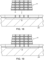
FIG. 18 is a sectional view depicting exemplary mounting of the die stack on a semiconductor die of the semiconductor wafer; -
FIG. 19 is a sectional view depicting the mounted die stack on a die of the semiconductor wafer; -
FIG. 20 is a sectional view depicting exemplary dummy component mounting; -
FIG. 21 is a sectional view depicting exemplary molding material molding; and -
FIG. 22 is a sectional view depicting exemplary I/O mounting. - A conventional die stacking technique stacks dies sequentially, one die on top of the first die and so on up to the top die of the stack. Where through-die-vias (TDVs) are used for die to die electrical connections, a reveal process is necessary to reveal the TDVs of one die before the next die is mounted. This is typically done in one conventional process by creating a reconstituted wafer of previously singulated dies and then performing the reveal process on the reconstituted wafer. Often times a gap filling process is necessary to avoid adversely affecting the lower dies in the stack during reveal of the TDVs of the current topmost die in the stack. However, the techniques disclosed herein enable the creation of die stacks where TDV reveals can always be performed at the wafer level without the need to resort to reconstitution. Gap filling processes during stack creation are not necessary.
- In the drawings described below, reference numerals are generally repeated where identical elements appear in more than one figure. Turning now to the drawings, and in particular to
FIG. 1 which is a sectional view of an exemplarysemiconductor die device 10 that includes astack 15 of multiple semiconductor dies mounted on another semiconductor die 20. Thesemiconductor die device 10 can be mounted on a circuit board (not shown), such as a package substrates, a system board, a daughter board, a circuit cards or other. Thestack 15 in this illustrative arrangement consists of four semiconductor dies 25, 30, 35 and 40, but of course, other numbers are possible. The semiconductor dies 20, 25, 30, 35 and 40 include respective back end of line structures (BEOL) 45, 50, 55, 60 and 65. TheBEOLs semiconductor die stack 15 can have different footprints or approximately the same footprint. In the illustrated arrangement, the semiconductor dies 25, 30, 35 and 40 of thesemiconductor die stack 15 can have successively smaller footprints, that is, the semiconductor die 40 is smaller than thesemiconductor die 35, which in-turn is smaller than the semiconductor die 30 and so on. - Electrical connections between the semiconductor die 25 and the
semiconductor die 20 are by way ofplural interconnects 70. The semiconductor die 30 is electrically connected to the semiconductor die 25 by way ofplural interconnects 75. In addition, sets ofinterconnects interconnects layer 100 and interconnects 80 between semiconductor dies 35 and 30 are such that mounting the first semiconductor die on the second semiconductor die includes forming a firstinsulating bonding layer 100 having a first glass layer and a second glass layer between and bonding the first semiconductor die and the second semiconductor die and annealing to bond the first glass layer to the second glass layer and to metallurgically bond conductor structures of the first semiconductor die and conductor structures of the second semiconductor die. - The semiconductor dies 20, 25, 30, 35 and 40 can be any of a variety of integrated circuits. A non-exhaustive list of examples includes processors, such as microprocessors, graphics processing units, accelerated processing units that combine aspects of both, memory devices, an application integrated specific circuit or other. In one arrangement, the semiconductor die 20 can be a processor and the semiconductor dies 25, 30, 35 and 40 can be memory dies, such as DRAM, SRAM or other.
- To facilitate heat transfer from the semiconductor die 20,
dummy components adhesive layers dummy components semiconductor die device 10. Theadhesive layers adhesive layers - A
molding material 130 at least laterally encases the semiconductor diestack 15 and is positioned between the semiconductor diestack 15 and thedummy components molding material 130 can have a molding temperature of about 165 °C. Two commercial variants are Sumitomo EME-G750 and G760. Well-known compression molding techniques can be used to mold themolding material 130. - Through die electrical conductivity is provided by plural through-die-vias (TDV). For example, the semiconductor die 20 includes
plural TDVs 135 that are connected to theinterconnects 70 and to I/Os 140. The TDVs 135 (and any related disclosed conductors, such as pillars and pads) can be composed of various conductor materials, such as copper, aluminum, silver, gold, platinum, palladium or others. Typically, eachTDV 135 is surrounded laterally by a liner layer (not shown) of SiOx or other insulator and a barrier layer of TiN or other barrier materials. The semiconductor die 25 similarly includesTDVs 145 that are connected between theinterconnects TDVs 150 that connect between theinterconnects TDVs 155 that connect between theinterconnects plural TDVs 160, which in this illustrative arrangement are not revealed, but of course could be revealed using the thinning/reveal processes disclosed herein to facilitate interconnection with yet another die stacked on top of thestack 15 if desired. The I/Os 140 enable thesemiconductor die device 10 to interface electrically with another component such as a circuit board or other device, and can be solder bumps, balls or other types of interconnect structures. Well-known lead free solders, such as Sn-Ag, Sn-Ag-Cu or others can be used for the I/Os 140 and other solder structures disclosed herein. - Additional details of an exemplary arrangement of the
interconnects 75 and insulatinglayer 95 will be described now in conjunction withFIGS. 2 . Note thatFIG. 2 is the portion ofFIG. 1 circumscribed by the small dashedrectangle 165 shown at greater magnification. The following description will be illustrative of theother interconnects layers FIG. 2 , each of theinterconnects 75 consists of a bumpless oxide hybrid bond. In this regard, theinterconnect 75 between the semiconductor die 25 and theBEOL 55 of the semiconductor die 30 is made up of a metallurgical bond between abond pad 170 of theBEOL 55 and abond pad 172 of the semiconductor die 25. Thebond pad 170 is connected to theTDV 150 and thebond pad 172 is connected to theTDV 145. In addition, the insulatingstructure 95 joins the semiconductor die 25 to the semiconductor die 30 and consists of aglass layer 175, such as SiOx, of the semiconductor die 30 and anotherglass layer 180, such as silicon oxynitride, of the semiconductor die 25. The glass layers 175 and 180 are preferably deposited on the semiconductor dies 25 and 30, respectively, by plasma enhanced chemical vapor deposition (PECVD). Thebond pad 170 is positioned in theglass layer 175 and thebond pad 172 is positioned in theglass layer 180. Thebond pad 170 and thebond pad 172 are metallurgically bonded by way of an anneal process. In this regard, the semiconductor die 30 is brought down or otherwise positioned on the semiconductor die 25 so that theglass layer 175 is on or in very close proximity to theglass layer 180 and thebond pad 170 is on or in very close proximity to thebond pad 172. Thereafter, an anneal process is performed, which produces a transitory thermal expansion of thebond pads bond pads glass layer 175 and theglass layer 180. An exemplary anneal is performed at about 300° C for about 30 to 60 minutes to form the requisite oxynitride-oxide bonds and metal-metal bonds. In another alternative, conductive pillars on each of two adjacent stacked dies can be thermal compression bonded. In another alternative arrangement, direction oxide bond and TSV last connection can be used. In this technique, facing sides of each two adjacent stacked dies each receive an oxide film. The oxide films are subsequently planarized using chemical mechanical polishing and then plasma treated to become hydrophillic. The oxide surfaces are next placed together and annealed to form a bond. - An exemplary process flow for fabricating the
semiconductor die device 10 depicted inFIG. 1 will now be described in conjunction withFIGS. 3, 4, 5 ,6, 7, 8, 9 ,10, 11 ,12, 13, 14 ,15, 16, 17 ,18, 19 ,20, 21 and22 . Attention is initially turned toFIG. 3 , which is a sectional view of a portion of asemiconductor wafer 185. Thesemiconductor wafer 185 can include scores or hundreds of individual semiconductor dies in addition to the semiconductor die 35. Here, the semiconductor die 35 is demarcated by dicingstreets semiconductor wafer 185 will occur. Of course there are additional dicing streets that are not associated with the semiconductor die 35, which are not visible inFIG. 3 . Thewafer 185 has been processed to the point where theBEOL 60 of the semiconductor die 35 is complete along with theTDVs 155. However, thewafer 185 has yet to undergo a thinning process to reveal theTDVs 155. - Next and as shown in
FIG. 4 , thewafer 185 is flipped over from the orientation depicted inFIG. 3 and mounted on, and with theBEOL 60 facing towards, acarrier wafer 200. Thecarrier wafer 200 can be composed of silicon, various glasses, or other types of semiconductor materials. Thewafer 185 can be secured to thecarrier wafer 200 by way of an adhesive 202 applied to thecarrier wafer 200. The adhesive 202 is preferably a well-known reversible adhesive, such as light activated or thermally activated adhesives, that can be reversed so that later thecarrier wafer 200 can be removed. Optionally, bonding agents that require chemical and/or mechanical removal techniques could be used. - Next and as shown in
FIG. 5 , thewafer 185 undergoes a thinning process to reveal theTDVs 155. Various thinning/reveal processes can be used. In one arrangement, the reveal process is preferably a soft reveal wherein thewafer 185 and the semiconductor die 35 are subjected to a grinding process to just above the tops of the through-die vias 155, followed by an etch back to reveal the tops of the through-die-vias 155. Next, a deposition process is used to establish a thin glass layer (not visible but like theglass layer 180 depicted inFIG. 2 and described above). The thin glass layer is preferably deposited using PECVD and then subjected to CMP. Thecarrier wafer 200 facilitates these various grinding, etching, deposition and CMP processes. In one so-called "hard reveal" technique, a grinding process is used to expose theTDVs 155 followed by an etch back of a small amount of the wafer 185 (silicon or otherwise), followed by a thin oxide growth or deposition or a thin silicon nitride deposition by CVD and again followed by a chemical mechanical planarization in order to finalize the through-die via reveal. The first technique avoids exposing thesubstrate semiconductor wafer 185 to loose copper or other metal particles that can be liberated during a hard reveal. - Next and as shown in
FIG. 6 , the semiconductor die 40 is mounted on the semiconductor die 35 of thewafer 185. The semiconductor die 40 is a singulated device that was formally part of another semiconductor wafer (not shown) that was processed to establish theBEOL 65 of the semiconductor die 40 as well as theunexposed TDVs 160 thereof. Theinterconnects 85 and the insulatinglayer 105 are fabricated at this point using the techniques disclosed elsewhere herein in conjunction withFIG. 2 and for theinterconnects 75 and the insulatinglayer 95. Of course if the aforementioned bumpless hybrid bond process described in conjunction withFIG. 2 is used, then the mounting process will be preceded by application of a glass layer (not visible but like theglass layer 175 depicted inFIG. 2 and described elsewhere herein) on the semiconductor die 40 (or the wafer of which it was formally a part). Optionally, if theinterconnects 85 are solder bumps, solder micro bumps or other types of interconnects then an appropriate mounting and reflow process will be performed at this stage to establish theinterconnects 85. - Next and as shown in
FIG. 7 , the semiconductor die 35 is singulated from thewafer 185 following the initial removal of thecarrier wafer 200 shown inFIG. 6 to yield the combination of the semiconductor dies 35 and 40. The removal process for thecarrier wafer 200 will depend on the type of the adhesive 202. Examples include thermal release, chemical release, mechanical peel off or laser induced removal. This combination of semiconductor dies 35 and 40 is now a stackable element that will be placed on the semiconductor die 30 as described more fully below. - The fabrication of the semiconductor die 30 will now be described in conjunction with
FIGS. 8, 9 and10 . Anothersemiconductor wafer 205 includes multitudes of semiconductor dies including the semiconductor die 30 which has been processed using well known techniques to establish theBEOL 55 and theTDVs 150 thereof. Like thesemiconductor wafer 185, thewafer 205 has not undergone a thinning process at this point to reveal theTDVs 150. The semiconductor die 30 is demarcated by dicingstreets FIG. 8 . Next and as shown inFIG. 9 , thesemiconductor wafer 205 is flipped over from the orientation shown inFIG. 8 and mounted on anothercarrier wafer 220 such that theBEOL 55 is facing towards thecarrier wafer 220. Thecarrier wafer 220 can be composed of silicon, various glasses, or other types of semiconductor materials. Thesemiconductor wafer 205 can be secured to thecarrier wafer 220 by way of an adhesive applied to thecarrier wafer 220. The adhesive can be like the adhesive 202 described above, and is not shown for simplicity of illustration. Next and as shown inFIG. 10 , thesemiconductor wafer 205 undergoes a thinning process to reveal theTDVs 150 of the semiconductor die 30. The reveal can be by way of the thinning/reveal processes disclosed above in conjunction withFIG. 5 . Thewafer 205 is now ready to have the combination of the semiconductor dies 35 and 40 mounted onto the semiconductor die 30 thereof. Next and as shown inFIG. 11 , the combination of the semiconductor dies 35 and 40 is mounted on the semiconductor die 30 of thewafer 205. The mounting process is like the mounting process described above in conjunction with mounting the semiconductor die 40 on the semiconductor die 35. In this regard, theinterconnects 80 and the insulatinglayer 100 are established at this point using the techniques described above in conjunction with theinterconnects 75 and the insulatingstructure 95 depicted inFIGS. 1 and 2 . Thecarrier wafer 220 is removed using a process suitable for the adhesive (not visible) that bonded to thesemiconductor wafer 205, such as the types disclosed elsewhere herein. The semiconductor die 30 is then singulated from thewafer 205 to yield the singulated combination of the semiconductor dies 30, 35 and 40 as shown inFIG. 12 . Singulation can be by mechanical sawing, laser cutting or other techniques. - Next and as shown in
FIG. 13 , the combination of the semiconductor dies 30, 35 and 40 is mounted on the semiconductor die 25, which is at this stage still part of asemiconductor wafer 225 that has been processed like thesemiconductor wafers carrier wafer 230 such that thewafer 225 has undergone a thinning process to reveal theTDVs 145 of the semiconductor die 25 and the BEOL 50 is facing towards thecarrier wafer 230. The mounting process for the semiconductor dies 30, 35 and 40 to the semiconductor die 25 is like the process to mount the combination of the semiconductor dies 35 and 40 to the semiconductor die 30 just described. Following the mounting process, thecarrier wafer 230 is removed and the semiconductor die 25 singulated from thesemiconductor wafer 225 to yield the completed semiconductor diestack 15 shown inFIG. 14 . The semiconductor diestack 15 consisting of the semiconductor dies 25, 30, 35 and 40 is now ready to be mounted on the semiconductor die 20 shown inFIG. 1 . - Referring now to
FIG. 15 , the semiconductor die 20 is initially part of asemiconductor wafer 235 and is demarcated by dicingstreets wafer 235 has been processed such that theBEOL 45 of the semiconductor die 20 and theTDVs 135 have been fabricated. However, thewafer 235 is yet to undergo a thinning process to reveal theTDVs 135. Next and as shown inFIG. 16 , thesemiconductor wafer 235 is flipped over from the orientation inFIG. 15 and mounted on acarrier wafer 250 with theBEOL 45 facing towards thecarrier wafer 250. Thesemiconductor wafer 235 can be secured to thecarrier wafer 250 using an adhesive applied to thecarrier wafer 250. The adhesive can be like the adhesive 202 described above, and is not shown for simplicity of illustration. Next and as shown inFIG. 17 , with thecarrier wafer 250 in place, thewafer 235 undergoes a thinning process to reveal theTDVs 135 of the semiconductor die 20. The reveal can be by way of the thinning/reveal processes disclosed above in conjunction withFIG. 5 . Next and as shown inFIG. 18 , the semiconductor diestack 15 is mounted on the semiconductor die 20 of thewafer 235. This mounting process establishes theinterconnects 70 and the insulating structure 90 and can be by way of the aforementioned hybrid bonding process or another process if theinterconnect 70 are not hybrid bonds. The mountedstack 15 is depicted on the semiconductor die 20 inFIG. 19 . Next and as shown inFIG. 20 , with thecarrier wafer 250 still in place, thedummy components semiconductor wafer 235 on either side of the semiconductor diestack 15. Thedummy components stack 15. However, efficiencies can be achieved if thedummy components stack 15 and other dummy components (not visible) that will be used by adjacent semiconductor die stacks (not visible) on thesemiconductor wafer 235. Indeed, note that during a subsequent singulation process, the dicingstreets dummy components - Next and as shown in
FIG. 21 , with thecarrier wafer 250 in place, thesemiconductor wafer 235 undergoes a molding process to establish themolding material 130. This molding process can establish themolding material 130 with an upper surface that is planar with thedummy components molding material 130 can cover thedummy components stack 15 and then a subsequent grinding process can be used to planarize themolding material 130 and thedummy components FIG. 22 , the I/O structures 140 are fabricated or otherwise attached to the semiconductor die 20. This can entail a pick and place and reflow or a solder stencil or other process to establish the I/O structures 140. Prior to attaching or otherwise fabricating the I/O structures 140, thecarrier wafer 250 depicted inFIG. 21 is removed using the carrier wafer removal techniques disclosed elsewhere herein. The semiconductor die 20 is next singulated using the techniques disclosed elsewhere herein from thesemiconductor wafer 235 at the dicingstreets device 10 shown inFIG. 1 .
Claims (10)
- A method of manufacturing a semiconductor die device (10), comprising:mounting a first semiconductor die (35) on a second semiconductor die (30) of a first semiconductor wafer (205), the mounting of the first semiconductor die on the second semiconductor die including forming a first insulating bonding layer (100) having a first glass layer and a second glass layer between and bonding the first semiconductor die and the second semiconductor die and annealing to bond the first glass layer to the second glass layer and to metallurgically bond conductor structures of the first semiconductor die and conductor structures of the second semiconductor die;singulating the second semiconductor die (30) from the first semiconductor wafer (205) to yield a first die stack;mounting the second semiconductor die (30) of the first die stack on a third semiconductor die (25) of a second semiconductor wafer (225);singulating the third semiconductor die (25) from the second semiconductor wafer (225) to yield a second die stack (15);mounting the second die stack (15) on a fourth semiconductor die (20) of a third semiconductor wafer (235);mounting a first dummy component (110) on the third semiconductor wafer (235) adjacent to a first side of the second die stack (15) and a second dummy component (115) on the third semiconductor wafer adjacent to a second side of the second die stack (15) opposite to the first side, the first dummy component and the second dummy component being mounted at least partially on the fourth semiconductor die (20) to facilitate heat transfer from the fourth semiconductor die (20); andmolding a material (130) positioned between the second die stack (15) and the first dummy component (110) and between the second die stack (15) and the second dummy component (115), wherein the molding material (130) at least partially encases the second die stack (15).
- The method of claim 1, comprising singulating the fourth semiconductor die (20) from the third semiconductor wafer (235) to yield a third die stack.
- The method of claim 1, comprising mounting the first semiconductor wafer (205) to a first carrier wafer (220) and revealing plural through-die-vias (150) of the second semiconductor die (30) prior to mounting the first semiconductor die (35) on the second semiconductor die (30).
- The method of claim 3, comprising mounting the second semiconductor wafer (225) to a second carrier wafer (230) and revealing plural through-die-vias (145) of the third semiconductor die (25) prior to mounting the second semiconductor die (30) on the third semiconductor die (25).
- The method of claim 1, wherein the bonding of the conductor structures of the first semiconductor die (35) and conductor structures of the second semiconductor die (30) establish plural interconnects between the first semiconductor die and the second semiconductor die.
- The method of claim 1, wherein mounting the second semiconductor die (30) of the first die stack on the third semiconductor die (25) comprises forming a second insulating bonding layer having a first glass layer and a second glass layer between and bonding the second semiconductor die (30) and the third semiconductor die (25) and annealing to bond the first glass layer to the second glass layer and to metallurgically bond conductor structures of the second semiconductor die and conductor structures of the third semiconductor die.
- The method of claim 1, wherein the fourth semiconductor die (20) has a first side facing the third semiconductor die (25) and another side opposite the first side, comprising fabricating plural I/Os (140) on the another side.
- The method of claim 1, wherein each of the first semiconductor die (35), the second semiconductor die (30) and the third semiconductor die (25) comprises a memory die and wherein the fourth semiconductor die (20) comprises a processor.
- The method of claim 1, wherein the first semiconductor die (35), the second semiconductor die (30) and the third semiconductor die (25) have the same footprint.
- The method of claim 1, wherein the first semiconductor die (35), the second semiconductor die (30), the third semiconductor die (25) and the fourth semiconductor die (20) have successively larger footprints.
Applications Claiming Priority (2)
| Application Number | Priority Date | Filing Date | Title |
|---|---|---|---|
| US15/991,573 US10727204B2 (en) | 2018-05-29 | 2018-05-29 | Die stacking for multi-tier 3D integration |
| PCT/US2019/024835 WO2019231549A1 (en) | 2018-05-29 | 2019-03-29 | Die stacking for multi-tier 3d integration |
Publications (3)
| Publication Number | Publication Date |
|---|---|
| EP3803972A1 EP3803972A1 (en) | 2021-04-14 |
| EP3803972A4 EP3803972A4 (en) | 2022-03-09 |
| EP3803972B1 true EP3803972B1 (en) | 2024-03-20 |
Family
ID=68692796
Family Applications (1)
| Application Number | Title | Priority Date | Filing Date |
|---|---|---|---|
| EP19810608.0A Active EP3803972B1 (en) | 2018-05-29 | 2019-03-29 | Die stacking for multi-tier 3d integration |
Country Status (6)
| Country | Link |
|---|---|
| US (2) | US10727204B2 (en) |
| EP (1) | EP3803972B1 (en) |
| JP (1) | JP7007496B2 (en) |
| KR (1) | KR102285215B1 (en) |
| CN (1) | CN112005371A (en) |
| WO (1) | WO2019231549A1 (en) |
Families Citing this family (49)
| Publication number | Priority date | Publication date | Assignee | Title |
|---|---|---|---|---|
| US11069734B2 (en) | 2014-12-11 | 2021-07-20 | Invensas Corporation | Image sensor device |
| US9741620B2 (en) | 2015-06-24 | 2017-08-22 | Invensas Corporation | Structures and methods for reliable packages |
| US10204893B2 (en) | 2016-05-19 | 2019-02-12 | Invensas Bonding Technologies, Inc. | Stacked dies and methods for forming bonded structures |
| CN108288616B (en) | 2016-12-14 | 2023-04-07 | 成真股份有限公司 | Chip package |
| US20180182665A1 (en) | 2016-12-28 | 2018-06-28 | Invensas Bonding Technologies, Inc. | Processed Substrate |
| US10879212B2 (en) | 2017-05-11 | 2020-12-29 | Invensas Bonding Technologies, Inc. | Processed stacked dies |
| US10217720B2 (en) | 2017-06-15 | 2019-02-26 | Invensas Corporation | Multi-chip modules formed using wafer-level processing of a reconstitute wafer |
| US10447274B2 (en) | 2017-07-11 | 2019-10-15 | iCometrue Company Ltd. | Logic drive based on standard commodity FPGA IC chips using non-volatile memory cells |
| US10957679B2 (en) | 2017-08-08 | 2021-03-23 | iCometrue Company Ltd. | Logic drive based on standardized commodity programmable logic semiconductor IC chips |
| US10630296B2 (en) | 2017-09-12 | 2020-04-21 | iCometrue Company Ltd. | Logic drive with brain-like elasticity and integrality based on standard commodity FPGA IC chips using non-volatile memory cells |
| US10608642B2 (en) | 2018-02-01 | 2020-03-31 | iCometrue Company Ltd. | Logic drive using standard commodity programmable logic IC chips comprising non-volatile radom access memory cells |
| US11276676B2 (en) | 2018-05-15 | 2022-03-15 | Invensas Bonding Technologies, Inc. | Stacked devices and methods of fabrication |
| US12476637B2 (en) | 2018-05-24 | 2025-11-18 | iCometrue Company Ltd. | Logic drive using standard commodity programmable logic IC chips |
| US10727204B2 (en) * | 2018-05-29 | 2020-07-28 | Advances Micro Devices, Inc. | Die stacking for multi-tier 3D integration |
| US11158606B2 (en) | 2018-07-06 | 2021-10-26 | Invensas Bonding Technologies, Inc. | Molded direct bonded and interconnected stack |
| US11462419B2 (en) | 2018-07-06 | 2022-10-04 | Invensas Bonding Technologies, Inc. | Microelectronic assemblies |
| US12406959B2 (en) | 2018-07-26 | 2025-09-02 | Adeia Semiconductor Bonding Technologies Inc. | Post CMP processing for hybrid bonding |
| US11296044B2 (en) | 2018-08-29 | 2022-04-05 | Invensas Bonding Technologies, Inc. | Bond enhancement structure in microelectronics for trapping contaminants during direct-bonding processes |
| US11309334B2 (en) | 2018-09-11 | 2022-04-19 | iCometrue Company Ltd. | Logic drive using standard commodity programmable logic IC chips comprising non-volatile random access memory cells |
| US10937762B2 (en) | 2018-10-04 | 2021-03-02 | iCometrue Company Ltd. | Logic drive based on multichip package using interconnection bridge |
| US11616046B2 (en) | 2018-11-02 | 2023-03-28 | iCometrue Company Ltd. | Logic drive based on chip scale package comprising standardized commodity programmable logic IC chip and memory IC chip |
| US11211334B2 (en) | 2018-11-18 | 2021-12-28 | iCometrue Company Ltd. | Logic drive based on chip scale package comprising standardized commodity programmable logic IC chip and memory IC chip |
| US11476213B2 (en) | 2019-01-14 | 2022-10-18 | Invensas Bonding Technologies, Inc. | Bonded structures without intervening adhesive |
| US11296053B2 (en) | 2019-06-26 | 2022-04-05 | Invensas Bonding Technologies, Inc. | Direct bonded stack structures for increased reliability and improved yield in microelectronics |
| US11227838B2 (en) | 2019-07-02 | 2022-01-18 | iCometrue Company Ltd. | Logic drive based on multichip package comprising standard commodity FPGA IC chip with cooperating or supporting circuits |
| US11887930B2 (en) | 2019-08-05 | 2024-01-30 | iCometrue Company Ltd. | Vertical interconnect elevator based on through silicon vias |
| US12080672B2 (en) | 2019-09-26 | 2024-09-03 | Adeia Semiconductor Bonding Technologies Inc. | Direct gang bonding methods including directly bonding first element to second element to form bonded structure without adhesive |
| DE102021101251A1 (en) | 2020-03-31 | 2021-09-30 | Taiwan Semiconductor Manufacturing Co., Ltd. | PROTECTION AGAINST ANTENNA EFFECTS AND PROTECTION AGAINST ELECTROSTATIC DISCHARGE FOR THREE-DIMENSIONAL INTEGRATED CIRCUITS |
| US11437708B2 (en) | 2020-03-31 | 2022-09-06 | Taiwan Semiconductor Manufacturing Company, Ltd. | Antenna effect protection and electrostatic discharge protection for three-dimensional integrated circuit |
| US11631647B2 (en) * | 2020-06-30 | 2023-04-18 | Adeia Semiconductor Bonding Technologies Inc. | Integrated device packages with integrated device die and dummy element |
| US11728273B2 (en) | 2020-09-04 | 2023-08-15 | Adeia Semiconductor Bonding Technologies Inc. | Bonded structure with interconnect structure |
| US11764177B2 (en) | 2020-09-04 | 2023-09-19 | Adeia Semiconductor Bonding Technologies Inc. | Bonded structure with interconnect structure |
| TW202240808A (en) | 2021-01-08 | 2022-10-16 | 成真股份有限公司 | Micro heat pipes for use in integrated circuit chip package |
| US11594460B2 (en) * | 2021-03-11 | 2023-02-28 | Taiwan Semiconductor Manufacturing Company, Ltd. | Semiconductor package and method of fabricating the same |
| KR102894753B1 (en) * | 2021-05-06 | 2025-12-02 | 삼성전자주식회사 | Semiconductor package |
| US12176278B2 (en) | 2021-05-30 | 2024-12-24 | iCometrue Company Ltd. | 3D chip package based on vertical-through-via connector |
| US11935871B2 (en) * | 2021-08-30 | 2024-03-19 | Taiwan Semiconductor Manufacturing Company, Ltd. | Semiconductor package and method of fabricating the same |
| US12424574B2 (en) | 2021-09-01 | 2025-09-23 | Micron Technology, Inc. | Polymer coated semiconductor devices and hybrid bonding to form semiconductor assemblies |
| KR20230039139A (en) | 2021-09-13 | 2023-03-21 | 삼성전자주식회사 | 3D(3-Dimentional) stack chip, and semiconductor package comprising the stack chip |
| US12268012B2 (en) | 2021-09-24 | 2025-04-01 | iCometrue Company Ltd. | Multi-output look-up table (LUT) for use in coarse-grained field-programmable-gate-array (FPGA) integrated-circuit (IC) chip |
| US12191282B2 (en) * | 2021-11-30 | 2025-01-07 | Taiwan Semiconductor Manufacturing Company, Ltd. | Shared pad/bridge layout for a 3D IC |
| US20230207525A1 (en) * | 2021-12-24 | 2023-06-29 | Intel Corporation | Ic die stacking with mixed hybrid and solder bonding |
| KR20240006828A (en) * | 2022-07-07 | 2024-01-16 | 에스케이하이닉스 주식회사 | Stack packages including semiconductor dies and encapsulant |
| US20240113070A1 (en) * | 2022-09-30 | 2024-04-04 | Advanced Micro Devices, Inc. | Integrating devices into a carrier wafer for three dimensionally stacked semiconductor devices |
| US20240304579A1 (en) * | 2023-03-06 | 2024-09-12 | Macronix International Co., Ltd. | Semiconductor device and method for forming the same |
| US20240371818A1 (en) * | 2023-05-01 | 2024-11-07 | Taiwan Semiconductor Manufacturing Co., Ltd. | Edge fill for stacked structure |
| WO2025080293A2 (en) * | 2023-05-12 | 2025-04-17 | Massachusetts Institute Of Technology | 3d processor |
| KR20250033920A (en) | 2023-09-01 | 2025-03-10 | 삼성전자주식회사 | Semiconductor package and method for fabricating the same |
| US20250157830A1 (en) * | 2023-11-09 | 2025-05-15 | Asmpt Singapore Pte. Ltd. | Method for manufacturing integrated device packages |
Family Cites Families (53)
| Publication number | Priority date | Publication date | Assignee | Title |
|---|---|---|---|---|
| JP3065753B2 (en) | 1991-12-04 | 2000-07-17 | イビデン株式会社 | Resin sealing method for semiconductor integrated circuit bare chip, semiconductor device |
| US5901041A (en) | 1997-12-02 | 1999-05-04 | Northern Telecom Limited | Flexible integrated circuit package |
| JP2000311905A (en) | 1999-04-28 | 2000-11-07 | Nippon Inter Electronics Corp | Method for manufacturing composite semiconductor device |
| JP2000357768A (en) | 1999-06-17 | 2000-12-26 | Hitachi Ltd | Semiconductor device and manufacturing method thereof |
| US6589802B1 (en) | 1999-12-24 | 2003-07-08 | Hitachi, Ltd. | Packaging structure and method of packaging electronic parts |
| US6949822B2 (en) | 2000-03-17 | 2005-09-27 | International Rectifier Corporation | Semiconductor multichip module package with improved thermal performance; reduced size and improved moisture resistance |
| US6537482B1 (en) | 2000-08-08 | 2003-03-25 | Micron Technology, Inc. | Underfill and encapsulation of carrier substrate-mounted flip-chip components using stereolithography |
| JP2002124654A (en) | 2000-10-13 | 2002-04-26 | Mitsubishi Electric Corp | Solid-state imaging device |
| US6906415B2 (en) | 2002-06-27 | 2005-06-14 | Micron Technology, Inc. | Semiconductor device assemblies and packages including multiple semiconductor devices and methods |
| TW569416B (en) | 2002-12-19 | 2004-01-01 | Via Tech Inc | High density multi-chip module structure and manufacturing method thereof |
| US7122906B2 (en) | 2004-01-29 | 2006-10-17 | Micron Technology, Inc. | Die-wafer package and method of fabricating same |
| US7208342B2 (en) | 2004-05-27 | 2007-04-24 | Intel Corporation | Package warpage control |
| JP2006261566A (en) | 2005-03-18 | 2006-09-28 | Alps Electric Co Ltd | Electronic component holder and electronic component holding sheet, electronic module using these, electronic module laminate, electronic module manufacturing method, and inspection method |
| KR100621438B1 (en) * | 2005-08-31 | 2006-09-08 | 삼성전자주식회사 | Laminated chip package using photosensitive polymer and manufacturing method thereof |
| JP2007183164A (en) | 2006-01-06 | 2007-07-19 | Fujitsu Ltd | Semiconductor integrated circuit device and test method thereof |
| KR100743648B1 (en) * | 2006-03-17 | 2007-07-27 | 주식회사 하이닉스반도체 | Wafer Level System-in-Package Manufacturing Method |
| JP4391508B2 (en) | 2006-09-29 | 2009-12-24 | Okiセミコンダクタ株式会社 | Semiconductor device and manufacturing method of semiconductor device |
| JP2009158623A (en) | 2007-12-26 | 2009-07-16 | Panasonic Corp | Manufacturing method of semiconductor device |
| US7973310B2 (en) * | 2008-07-11 | 2011-07-05 | Chipmos Technologies Inc. | Semiconductor package structure and method for manufacturing the same |
| US8691626B2 (en) | 2010-09-09 | 2014-04-08 | Advanced Micro Devices, Inc. | Semiconductor chip device with underfill |
| KR20110044963A (en) | 2011-04-20 | 2011-05-03 | 앰코 테크놀로지 코리아 주식회사 | Stack Chip Package using TSV |
| US8552567B2 (en) * | 2011-07-27 | 2013-10-08 | Micron Technology, Inc. | Semiconductor die assemblies, semiconductor devices including same, and methods of fabrication |
| US8842945B2 (en) | 2011-08-09 | 2014-09-23 | Soitec | Methods of forming three dimensionally integrated semiconductor systems including photoactive devices and semiconductor-on-insulator substrates |
| US8372741B1 (en) | 2012-02-24 | 2013-02-12 | Invensas Corporation | Method for package-on-package assembly with wire bonds to encapsulation surface |
| US9768105B2 (en) | 2012-04-20 | 2017-09-19 | Taiwan Semiconductor Manufacturing Company, Ltd. | Rigid interconnect structures in package-on-package assemblies |
| US9502390B2 (en) | 2012-08-03 | 2016-11-22 | Invensas Corporation | BVA interposer |
| KR20140112674A (en) | 2013-03-14 | 2014-09-24 | 에스케이하이닉스 주식회사 | Fabricating method of stacked semiconductor package |
| US9312198B2 (en) | 2013-03-15 | 2016-04-12 | Intel Deutschland Gmbh | Chip package-in-package and method thereof |
| KR102077153B1 (en) * | 2013-06-21 | 2020-02-14 | 삼성전자주식회사 | Semiconductor packages having through electrodes and methods for fabricating the same |
| US9406588B2 (en) | 2013-11-11 | 2016-08-02 | Taiwan Semiconductor Manufacturing Company Ltd. | Semiconductor package and manufacturing method thereof |
| US9214454B2 (en) | 2014-03-31 | 2015-12-15 | Invensas Corporation | Batch process fabrication of package-on-package microelectronic assemblies |
| KR20150123420A (en) | 2014-04-24 | 2015-11-04 | 에스케이하이닉스 주식회사 | Semiconductor package and the method for manufacturing of the same |
| US9331021B2 (en) | 2014-04-30 | 2016-05-03 | Taiwan Semiconductor Manufacturing Company, Ltd. | Chip-on-wafer package and method of forming same |
| US9412675B2 (en) | 2014-05-19 | 2016-08-09 | Micron Technology, Inc. | Interconnect structure with improved conductive properties and associated systems and methods |
| US9620464B2 (en) | 2014-08-13 | 2017-04-11 | International Business Machines Corporation | Wireless communications package with integrated antennas and air cavity |
| WO2016118210A2 (en) | 2014-11-05 | 2016-07-28 | Massachusetts Institute Of Technology | Interconnect structures for assembly of multi-layer semiconductor devices |
| KR102411064B1 (en) | 2015-03-10 | 2022-06-21 | 삼성전자주식회사 | Methods for fabricating semiconductor devices having through electrodes and methods for fabricating the same |
| US9780079B2 (en) | 2015-04-30 | 2017-10-03 | Micron Technology, Inc. | Semiconductor die assembly and methods of forming thermal paths |
| JP2016225466A (en) | 2015-05-29 | 2016-12-28 | 株式会社東芝 | Semiconductor device and manufacturing method of semiconductor device |
| US9520333B1 (en) | 2015-06-22 | 2016-12-13 | Inotera Memories, Inc. | Wafer level package and fabrication method thereof |
| US9698790B2 (en) * | 2015-06-26 | 2017-07-04 | Advanced Micro Devices, Inc. | Computer architecture using rapidly reconfigurable circuits and high-bandwidth memory interfaces |
| US9601461B2 (en) | 2015-08-12 | 2017-03-21 | Semtech Corporation | Semiconductor device and method of forming inverted pyramid cavity semiconductor package |
| US9899355B2 (en) | 2015-09-30 | 2018-02-20 | Taiwan Semiconductor Manufacturing Co., Ltd. | Three-dimensional integrated circuit structure |
| US9972603B2 (en) * | 2015-12-29 | 2018-05-15 | Taiwan Semiconductor Manufacturing Co., Ltd. | Seal-ring structure for stacking integrated circuits |
| US9806014B2 (en) | 2016-01-27 | 2017-10-31 | Advanced Micro Devices, Inc. | Interposer with beyond reticle field conductor pads |
| US11373990B2 (en) * | 2016-02-29 | 2022-06-28 | Semtech Corporation | Semiconductor device and method of stacking semiconductor die for system-level ESD protection |
| US10026716B2 (en) * | 2016-04-15 | 2018-07-17 | Taiwan Semiconductor Manufacturing Company, Ltd. | 3DIC formation with dies bonded to formed RDLs |
| US20170330855A1 (en) * | 2016-05-13 | 2017-11-16 | Taiwan Semiconductor Manufacturing Company, Ltd. | System and Method for Immersion Bonding |
| US9865566B1 (en) | 2016-06-15 | 2018-01-09 | Taiwan Semiconductor Manufacturing Company Ltd. | Semiconductor structure and manufacturing method thereof |
| EP3288076B1 (en) | 2016-08-25 | 2021-06-23 | IMEC vzw | A semiconductor die package and method of producing the package |
| US9972611B2 (en) | 2016-09-30 | 2018-05-15 | Intel Corporation | Stacked semiconductor package having fault detection and a method for identifying a fault in a stacked package |
| US10008395B2 (en) * | 2016-10-19 | 2018-06-26 | Micron Technology, Inc. | Stacked semiconductor die assemblies with high efficiency thermal paths and molded underfill |
| US10727204B2 (en) * | 2018-05-29 | 2020-07-28 | Advances Micro Devices, Inc. | Die stacking for multi-tier 3D integration |
-
2018
- 2018-05-29 US US15/991,573 patent/US10727204B2/en active Active
-
2019
- 2019-03-29 CN CN201980025193.7A patent/CN112005371A/en active Pending
- 2019-03-29 JP JP2020554424A patent/JP7007496B2/en active Active
- 2019-03-29 WO PCT/US2019/024835 patent/WO2019231549A1/en not_active Ceased
- 2019-03-29 EP EP19810608.0A patent/EP3803972B1/en active Active
- 2019-03-29 KR KR1020207035323A patent/KR102285215B1/en active Active
-
2020
- 2020-07-16 US US16/930,761 patent/US10930621B2/en active Active
Also Published As
| Publication number | Publication date |
|---|---|
| EP3803972A1 (en) | 2021-04-14 |
| KR102285215B1 (en) | 2021-08-03 |
| US20190371763A1 (en) | 2019-12-05 |
| KR20210003923A (en) | 2021-01-12 |
| WO2019231549A1 (en) | 2019-12-05 |
| CN112005371A (en) | 2020-11-27 |
| JP7007496B2 (en) | 2022-01-24 |
| US10727204B2 (en) | 2020-07-28 |
| JP2021520071A (en) | 2021-08-12 |
| EP3803972A4 (en) | 2022-03-09 |
| US10930621B2 (en) | 2021-02-23 |
| US20200350292A1 (en) | 2020-11-05 |
Similar Documents
| Publication | Publication Date | Title |
|---|---|---|
| EP3803972B1 (en) | Die stacking for multi-tier 3d integration | |
| US20220384332A1 (en) | Semiconductor structure, package structure, and manufacturing method thereof | |
| US11562983B2 (en) | Package having multiple chips integrated therein and manufacturing method thereof | |
| US10312221B1 (en) | Stacked dies and dummy components for improved thermal performance | |
| US11164807B2 (en) | Arrangement and thermal management of 3D stacked dies | |
| US11855067B2 (en) | Integrated circuit package and method | |
| TWI556349B (en) | Structure of semiconductor device and method of manufacturing the same | |
| CN104979334B (en) | Semiconductor devices and method | |
| US20210082874A1 (en) | Package and manufacturing method of reconstructed wafer | |
| US10529693B2 (en) | 3D stacked dies with disparate interconnect footprints | |
| US9870975B1 (en) | Chip package with thermal dissipation structure and method for forming the same | |
| TW202310365A (en) | Three-dimensional device structure and forming method thereof | |
| US12125821B2 (en) | Package having multiple chips integrated therein and manufacturing method thereof | |
| KR102804065B1 (en) | Semiconductor package and method of manufacturing the semiconductor package | |
| US10790210B2 (en) | Semiconductor package and manufacturing method thereof | |
| US11908831B2 (en) | Method for manufacturing a wafer level chip scale package (WLCSP) | |
| CN114695272A (en) | Method for forming integrated circuit package | |
| US12550793B2 (en) | Integrated circuit package and method | |
| US20250343100A1 (en) | Semiconductor package and method |
Legal Events
| Date | Code | Title | Description |
|---|---|---|---|
| STAA | Information on the status of an ep patent application or granted ep patent |
Free format text: STATUS: THE INTERNATIONAL PUBLICATION HAS BEEN MADE |
|
| PUAI | Public reference made under article 153(3) epc to a published international application that has entered the european phase |
Free format text: ORIGINAL CODE: 0009012 |
|
| STAA | Information on the status of an ep patent application or granted ep patent |
Free format text: STATUS: REQUEST FOR EXAMINATION WAS MADE |
|
| 17P | Request for examination filed |
Effective date: 20201023 |
|
| AK | Designated contracting states |
Kind code of ref document: A1 Designated state(s): AL AT BE BG CH CY CZ DE DK EE ES FI FR GB GR HR HU IE IS IT LI LT LU LV MC MK MT NL NO PL PT RO RS SE SI SK SM TR |
|
| AX | Request for extension of the european patent |
Extension state: BA ME |
|
| DAV | Request for validation of the european patent (deleted) | ||
| DAX | Request for extension of the european patent (deleted) | ||
| A4 | Supplementary search report drawn up and despatched |
Effective date: 20220204 |
|
| RIC1 | Information provided on ipc code assigned before grant |
Ipc: H01L 23/00 20060101ALI20220131BHEP Ipc: H01L 23/31 20060101ALI20220131BHEP Ipc: H01L 21/78 20060101ALI20220131BHEP Ipc: H01L 21/768 20060101ALI20220131BHEP Ipc: H01L 25/065 20060101ALI20220131BHEP Ipc: H01L 21/98 20060101AFI20220131BHEP |
|
| STAA | Information on the status of an ep patent application or granted ep patent |
Free format text: STATUS: EXAMINATION IS IN PROGRESS |
|
| 17Q | First examination report despatched |
Effective date: 20221221 |
|
| REG | Reference to a national code |
Ref country code: DE Ref legal event code: R079 Free format text: PREVIOUS MAIN CLASS: H01L0025065000 Ipc: H01L0021980000 Ref document number: 602019048709 Country of ref document: DE |
|
| RIC1 | Information provided on ipc code assigned before grant |
Ipc: H01L 23/00 20060101ALI20230831BHEP Ipc: H01L 21/683 20060101ALI20230831BHEP Ipc: H01L 21/78 20060101ALI20230831BHEP Ipc: H01L 21/768 20060101ALI20230831BHEP Ipc: H01L 25/065 20060101ALI20230831BHEP Ipc: H01L 21/98 20060101AFI20230831BHEP |
|
| GRAP | Despatch of communication of intention to grant a patent |
Free format text: ORIGINAL CODE: EPIDOSNIGR1 |
|
| STAA | Information on the status of an ep patent application or granted ep patent |
Free format text: STATUS: GRANT OF PATENT IS INTENDED |
|
| INTG | Intention to grant announced |
Effective date: 20231020 |
|
| RIC1 | Information provided on ipc code assigned before grant |
Ipc: H01L 21/60 20060101ALI20231009BHEP Ipc: H01L 21/683 20060101ALI20231009BHEP Ipc: H01L 21/78 20060101ALI20231009BHEP Ipc: H01L 21/768 20060101ALI20231009BHEP Ipc: H01L 25/065 20060101ALI20231009BHEP Ipc: H01L 21/98 20060101AFI20231009BHEP |
|
| GRAS | Grant fee paid |
Free format text: ORIGINAL CODE: EPIDOSNIGR3 |
|
| GRAA | (expected) grant |
Free format text: ORIGINAL CODE: 0009210 |
|
| STAA | Information on the status of an ep patent application or granted ep patent |
Free format text: STATUS: THE PATENT HAS BEEN GRANTED |
|
| AK | Designated contracting states |
Kind code of ref document: B1 Designated state(s): AL AT BE BG CH CY CZ DE DK EE ES FI FR GB GR HR HU IE IS IT LI LT LU LV MC MK MT NL NO PL PT RO RS SE SI SK SM TR |
|
| REG | Reference to a national code |
Ref country code: GB Ref legal event code: FG4D |
|
| REG | Reference to a national code |
Ref country code: CH Ref legal event code: EP |
|
| REG | Reference to a national code |
Ref country code: DE Ref legal event code: R096 Ref document number: 602019048709 Country of ref document: DE |
|
| REG | Reference to a national code |
Ref country code: IE Ref legal event code: FG4D |
|
| P01 | Opt-out of the competence of the unified patent court (upc) registered |
Effective date: 20240312 |
|
| PG25 | Lapsed in a contracting state [announced via postgrant information from national office to epo] |
Ref country code: LT Free format text: LAPSE BECAUSE OF FAILURE TO SUBMIT A TRANSLATION OF THE DESCRIPTION OR TO PAY THE FEE WITHIN THE PRESCRIBED TIME-LIMIT Effective date: 20240320 |
|
| REG | Reference to a national code |
Ref country code: LT Ref legal event code: MG9D |
|
| PG25 | Lapsed in a contracting state [announced via postgrant information from national office to epo] |
Ref country code: GR Free format text: LAPSE BECAUSE OF FAILURE TO SUBMIT A TRANSLATION OF THE DESCRIPTION OR TO PAY THE FEE WITHIN THE PRESCRIBED TIME-LIMIT Effective date: 20240621 |
|
| PG25 | Lapsed in a contracting state [announced via postgrant information from national office to epo] |
Ref country code: RS Free format text: LAPSE BECAUSE OF FAILURE TO SUBMIT A TRANSLATION OF THE DESCRIPTION OR TO PAY THE FEE WITHIN THE PRESCRIBED TIME-LIMIT Effective date: 20240620 Ref country code: HR Free format text: LAPSE BECAUSE OF FAILURE TO SUBMIT A TRANSLATION OF THE DESCRIPTION OR TO PAY THE FEE WITHIN THE PRESCRIBED TIME-LIMIT Effective date: 20240320 |
|
| REG | Reference to a national code |
Ref country code: NL Ref legal event code: MP Effective date: 20240320 |
|
| PG25 | Lapsed in a contracting state [announced via postgrant information from national office to epo] |
Ref country code: RS Free format text: LAPSE BECAUSE OF FAILURE TO SUBMIT A TRANSLATION OF THE DESCRIPTION OR TO PAY THE FEE WITHIN THE PRESCRIBED TIME-LIMIT Effective date: 20240620 Ref country code: NO Free format text: LAPSE BECAUSE OF FAILURE TO SUBMIT A TRANSLATION OF THE DESCRIPTION OR TO PAY THE FEE WITHIN THE PRESCRIBED TIME-LIMIT Effective date: 20240620 Ref country code: LT Free format text: LAPSE BECAUSE OF FAILURE TO SUBMIT A TRANSLATION OF THE DESCRIPTION OR TO PAY THE FEE WITHIN THE PRESCRIBED TIME-LIMIT Effective date: 20240320 Ref country code: HR Free format text: LAPSE BECAUSE OF FAILURE TO SUBMIT A TRANSLATION OF THE DESCRIPTION OR TO PAY THE FEE WITHIN THE PRESCRIBED TIME-LIMIT Effective date: 20240320 Ref country code: GR Free format text: LAPSE BECAUSE OF FAILURE TO SUBMIT A TRANSLATION OF THE DESCRIPTION OR TO PAY THE FEE WITHIN THE PRESCRIBED TIME-LIMIT Effective date: 20240621 Ref country code: FI Free format text: LAPSE BECAUSE OF FAILURE TO SUBMIT A TRANSLATION OF THE DESCRIPTION OR TO PAY THE FEE WITHIN THE PRESCRIBED TIME-LIMIT Effective date: 20240320 Ref country code: BG Free format text: LAPSE BECAUSE OF FAILURE TO SUBMIT A TRANSLATION OF THE DESCRIPTION OR TO PAY THE FEE WITHIN THE PRESCRIBED TIME-LIMIT Effective date: 20240320 |
|
| REG | Reference to a national code |
Ref country code: AT Ref legal event code: MK05 Ref document number: 1668610 Country of ref document: AT Kind code of ref document: T Effective date: 20240320 |
|
| PG25 | Lapsed in a contracting state [announced via postgrant information from national office to epo] |
Ref country code: SE Free format text: LAPSE BECAUSE OF FAILURE TO SUBMIT A TRANSLATION OF THE DESCRIPTION OR TO PAY THE FEE WITHIN THE PRESCRIBED TIME-LIMIT Effective date: 20240320 Ref country code: LV Free format text: LAPSE BECAUSE OF FAILURE TO SUBMIT A TRANSLATION OF THE DESCRIPTION OR TO PAY THE FEE WITHIN THE PRESCRIBED TIME-LIMIT Effective date: 20240320 |
|
| PG25 | Lapsed in a contracting state [announced via postgrant information from national office to epo] |
Ref country code: NL Free format text: LAPSE BECAUSE OF FAILURE TO SUBMIT A TRANSLATION OF THE DESCRIPTION OR TO PAY THE FEE WITHIN THE PRESCRIBED TIME-LIMIT Effective date: 20240320 |
|
| PG25 | Lapsed in a contracting state [announced via postgrant information from national office to epo] |
Ref country code: NL Free format text: LAPSE BECAUSE OF FAILURE TO SUBMIT A TRANSLATION OF THE DESCRIPTION OR TO PAY THE FEE WITHIN THE PRESCRIBED TIME-LIMIT Effective date: 20240320 |
|
| PG25 | Lapsed in a contracting state [announced via postgrant information from national office to epo] |
Ref country code: IS Free format text: LAPSE BECAUSE OF FAILURE TO SUBMIT A TRANSLATION OF THE DESCRIPTION OR TO PAY THE FEE WITHIN THE PRESCRIBED TIME-LIMIT Effective date: 20240720 |
|
| PG25 | Lapsed in a contracting state [announced via postgrant information from national office to epo] |
Ref country code: PT Free format text: LAPSE BECAUSE OF FAILURE TO SUBMIT A TRANSLATION OF THE DESCRIPTION OR TO PAY THE FEE WITHIN THE PRESCRIBED TIME-LIMIT Effective date: 20240722 Ref country code: SM Free format text: LAPSE BECAUSE OF FAILURE TO SUBMIT A TRANSLATION OF THE DESCRIPTION OR TO PAY THE FEE WITHIN THE PRESCRIBED TIME-LIMIT Effective date: 20240320 |
|
| PG25 | Lapsed in a contracting state [announced via postgrant information from national office to epo] |
Ref country code: ES Free format text: LAPSE BECAUSE OF FAILURE TO SUBMIT A TRANSLATION OF THE DESCRIPTION OR TO PAY THE FEE WITHIN THE PRESCRIBED TIME-LIMIT Effective date: 20240320 |
|
| PG25 | Lapsed in a contracting state [announced via postgrant information from national office to epo] |
Ref country code: CZ Free format text: LAPSE BECAUSE OF FAILURE TO SUBMIT A TRANSLATION OF THE DESCRIPTION OR TO PAY THE FEE WITHIN THE PRESCRIBED TIME-LIMIT Effective date: 20240320 Ref country code: EE Free format text: LAPSE BECAUSE OF FAILURE TO SUBMIT A TRANSLATION OF THE DESCRIPTION OR TO PAY THE FEE WITHIN THE PRESCRIBED TIME-LIMIT Effective date: 20240320 |
|
| PG25 | Lapsed in a contracting state [announced via postgrant information from national office to epo] |
Ref country code: AT Free format text: LAPSE BECAUSE OF FAILURE TO SUBMIT A TRANSLATION OF THE DESCRIPTION OR TO PAY THE FEE WITHIN THE PRESCRIBED TIME-LIMIT Effective date: 20240320 |
|
| PG25 | Lapsed in a contracting state [announced via postgrant information from national office to epo] |
Ref country code: PL Free format text: LAPSE BECAUSE OF FAILURE TO SUBMIT A TRANSLATION OF THE DESCRIPTION OR TO PAY THE FEE WITHIN THE PRESCRIBED TIME-LIMIT Effective date: 20240320 |
|
| PG25 | Lapsed in a contracting state [announced via postgrant information from national office to epo] |
Ref country code: SK Free format text: LAPSE BECAUSE OF FAILURE TO SUBMIT A TRANSLATION OF THE DESCRIPTION OR TO PAY THE FEE WITHIN THE PRESCRIBED TIME-LIMIT Effective date: 20240320 |
|
| PG25 | Lapsed in a contracting state [announced via postgrant information from national office to epo] |
Ref country code: SM Free format text: LAPSE BECAUSE OF FAILURE TO SUBMIT A TRANSLATION OF THE DESCRIPTION OR TO PAY THE FEE WITHIN THE PRESCRIBED TIME-LIMIT Effective date: 20240320 Ref country code: SK Free format text: LAPSE BECAUSE OF FAILURE TO SUBMIT A TRANSLATION OF THE DESCRIPTION OR TO PAY THE FEE WITHIN THE PRESCRIBED TIME-LIMIT Effective date: 20240320 Ref country code: RO Free format text: LAPSE BECAUSE OF FAILURE TO SUBMIT A TRANSLATION OF THE DESCRIPTION OR TO PAY THE FEE WITHIN THE PRESCRIBED TIME-LIMIT Effective date: 20240320 Ref country code: PT Free format text: LAPSE BECAUSE OF FAILURE TO SUBMIT A TRANSLATION OF THE DESCRIPTION OR TO PAY THE FEE WITHIN THE PRESCRIBED TIME-LIMIT Effective date: 20240722 Ref country code: PL Free format text: LAPSE BECAUSE OF FAILURE TO SUBMIT A TRANSLATION OF THE DESCRIPTION OR TO PAY THE FEE WITHIN THE PRESCRIBED TIME-LIMIT Effective date: 20240320 Ref country code: IS Free format text: LAPSE BECAUSE OF FAILURE TO SUBMIT A TRANSLATION OF THE DESCRIPTION OR TO PAY THE FEE WITHIN THE PRESCRIBED TIME-LIMIT Effective date: 20240720 Ref country code: ES Free format text: LAPSE BECAUSE OF FAILURE TO SUBMIT A TRANSLATION OF THE DESCRIPTION OR TO PAY THE FEE WITHIN THE PRESCRIBED TIME-LIMIT Effective date: 20240320 Ref country code: EE Free format text: LAPSE BECAUSE OF FAILURE TO SUBMIT A TRANSLATION OF THE DESCRIPTION OR TO PAY THE FEE WITHIN THE PRESCRIBED TIME-LIMIT Effective date: 20240320 Ref country code: CZ Free format text: LAPSE BECAUSE OF FAILURE TO SUBMIT A TRANSLATION OF THE DESCRIPTION OR TO PAY THE FEE WITHIN THE PRESCRIBED TIME-LIMIT Effective date: 20240320 Ref country code: AT Free format text: LAPSE BECAUSE OF FAILURE TO SUBMIT A TRANSLATION OF THE DESCRIPTION OR TO PAY THE FEE WITHIN THE PRESCRIBED TIME-LIMIT Effective date: 20240320 |
|
| REG | Reference to a national code |
Ref country code: CH Ref legal event code: PL |
|
| PG25 | Lapsed in a contracting state [announced via postgrant information from national office to epo] |
Ref country code: LU Free format text: LAPSE BECAUSE OF NON-PAYMENT OF DUE FEES Effective date: 20240329 |
|
| PG25 | Lapsed in a contracting state [announced via postgrant information from national office to epo] |
Ref country code: LU Free format text: LAPSE BECAUSE OF NON-PAYMENT OF DUE FEES Effective date: 20240329 |
|
| PG25 | Lapsed in a contracting state [announced via postgrant information from national office to epo] |
Ref country code: IT Free format text: LAPSE BECAUSE OF FAILURE TO SUBMIT A TRANSLATION OF THE DESCRIPTION OR TO PAY THE FEE WITHIN THE PRESCRIBED TIME-LIMIT Effective date: 20240320 |
|
| REG | Reference to a national code |
Ref country code: BE Ref legal event code: MM Effective date: 20240331 |
|
| REG | Reference to a national code |
Ref country code: DE Ref legal event code: R097 Ref document number: 602019048709 Country of ref document: DE |
|
| PG25 | Lapsed in a contracting state [announced via postgrant information from national office to epo] |
Ref country code: IT Free format text: LAPSE BECAUSE OF FAILURE TO SUBMIT A TRANSLATION OF THE DESCRIPTION OR TO PAY THE FEE WITHIN THE PRESCRIBED TIME-LIMIT Effective date: 20240320 |
|
| PG25 | Lapsed in a contracting state [announced via postgrant information from national office to epo] |
Ref country code: MC Free format text: LAPSE BECAUSE OF FAILURE TO SUBMIT A TRANSLATION OF THE DESCRIPTION OR TO PAY THE FEE WITHIN THE PRESCRIBED TIME-LIMIT Effective date: 20240320 |
|
| PG25 | Lapsed in a contracting state [announced via postgrant information from national office to epo] |
Ref country code: DK Free format text: LAPSE BECAUSE OF FAILURE TO SUBMIT A TRANSLATION OF THE DESCRIPTION OR TO PAY THE FEE WITHIN THE PRESCRIBED TIME-LIMIT Effective date: 20240320 |
|
| PG25 | Lapsed in a contracting state [announced via postgrant information from national office to epo] |
Ref country code: BE Free format text: LAPSE BECAUSE OF NON-PAYMENT OF DUE FEES Effective date: 20240331 |
|
| PG25 | Lapsed in a contracting state [announced via postgrant information from national office to epo] |
Ref country code: IE Free format text: LAPSE BECAUSE OF NON-PAYMENT OF DUE FEES Effective date: 20240329 |
|
| PLBE | No opposition filed within time limit |
Free format text: ORIGINAL CODE: 0009261 |
|
| STAA | Information on the status of an ep patent application or granted ep patent |
Free format text: STATUS: NO OPPOSITION FILED WITHIN TIME LIMIT |
|
| PG25 | Lapsed in a contracting state [announced via postgrant information from national office to epo] |
Ref country code: MC Free format text: LAPSE BECAUSE OF FAILURE TO SUBMIT A TRANSLATION OF THE DESCRIPTION OR TO PAY THE FEE WITHIN THE PRESCRIBED TIME-LIMIT Effective date: 20240320 Ref country code: IE Free format text: LAPSE BECAUSE OF NON-PAYMENT OF DUE FEES Effective date: 20240329 Ref country code: DK Free format text: LAPSE BECAUSE OF FAILURE TO SUBMIT A TRANSLATION OF THE DESCRIPTION OR TO PAY THE FEE WITHIN THE PRESCRIBED TIME-LIMIT Effective date: 20240320 Ref country code: BE Free format text: LAPSE BECAUSE OF NON-PAYMENT OF DUE FEES Effective date: 20240331 Ref country code: CH Free format text: LAPSE BECAUSE OF NON-PAYMENT OF DUE FEES Effective date: 20240331 |
|
| 26N | No opposition filed |
Effective date: 20241223 |
|
| PGFP | Annual fee paid to national office [announced via postgrant information from national office to epo] |
Ref country code: DE Payment date: 20250220 Year of fee payment: 7 |
|
| PG25 | Lapsed in a contracting state [announced via postgrant information from national office to epo] |
Ref country code: SI Free format text: LAPSE BECAUSE OF FAILURE TO SUBMIT A TRANSLATION OF THE DESCRIPTION OR TO PAY THE FEE WITHIN THE PRESCRIBED TIME-LIMIT Effective date: 20240320 |
|
| PG25 | Lapsed in a contracting state [announced via postgrant information from national office to epo] |
Ref country code: FR Free format text: LAPSE BECAUSE OF NON-PAYMENT OF DUE FEES Effective date: 20240520 |
|
| PGFP | Annual fee paid to national office [announced via postgrant information from national office to epo] |
Ref country code: GB Payment date: 20250311 Year of fee payment: 7 |
|
| PG25 | Lapsed in a contracting state [announced via postgrant information from national office to epo] |
Ref country code: CY Free format text: LAPSE BECAUSE OF FAILURE TO SUBMIT A TRANSLATION OF THE DESCRIPTION OR TO PAY THE FEE WITHIN THE PRESCRIBED TIME-LIMIT; INVALID AB INITIO Effective date: 20190329 |
|
| PG25 | Lapsed in a contracting state [announced via postgrant information from national office to epo] |
Ref country code: HU Free format text: LAPSE BECAUSE OF FAILURE TO SUBMIT A TRANSLATION OF THE DESCRIPTION OR TO PAY THE FEE WITHIN THE PRESCRIBED TIME-LIMIT; INVALID AB INITIO Effective date: 20190329 |
|
| REG | Reference to a national code |
Ref country code: DE Ref legal event code: R079 Ref document number: 602019048709 Country of ref document: DE Free format text: PREVIOUS MAIN CLASS: H01L0021980000 Ipc: H10W0090240000 |
|
| PG25 | Lapsed in a contracting state [announced via postgrant information from national office to epo] |
Ref country code: TR Free format text: LAPSE BECAUSE OF FAILURE TO SUBMIT A TRANSLATION OF THE DESCRIPTION OR TO PAY THE FEE WITHIN THE PRESCRIBED TIME-LIMIT Effective date: 20240320 |