EP2856528B1 - Metal complexes comprising condensed heteroaromatic rings - Google Patents
Metal complexes comprising condensed heteroaromatic rings Download PDFInfo
- Publication number
- EP2856528B1 EP2856528B1 EP13719398.3A EP13719398A EP2856528B1 EP 2856528 B1 EP2856528 B1 EP 2856528B1 EP 13719398 A EP13719398 A EP 13719398A EP 2856528 B1 EP2856528 B1 EP 2856528B1
- Authority
- EP
- European Patent Office
- Prior art keywords
- atoms
- group
- organic
- substituents
- compound
- Prior art date
- Legal status (The legal status is an assumption and is not a legal conclusion. Google has not performed a legal analysis and makes no representation as to the accuracy of the status listed.)
- Active
Links
- 0 CCCC1=CC=CC=CC=CC=C1CCC(C(C([C@@](CC)(C1(C)CC)*1(*1C2=C(*)C(*)=*1)*1c2c(*)c(*)c(*)c1*)=CC=C*)=C(CCCCCCC*)NC)=C Chemical compound CCCC1=CC=CC=CC=CC=C1CCC(C(C([C@@](CC)(C1(C)CC)*1(*1C2=C(*)C(*)=*1)*1c2c(*)c(*)c(*)c1*)=CC=C*)=C(CCCCCCC*)NC)=C 0.000 description 40
- WHKACFUJNYOJPD-UHFFFAOYSA-N Clc1ccc2nccnc2n1 Chemical compound Clc1ccc2nccnc2n1 WHKACFUJNYOJPD-UHFFFAOYSA-N 0.000 description 2
- QIVOWZKSYSRQFK-UHFFFAOYSA-N OB(C(C1)C=Cc2c1c(cccc1)c1[o]2)O Chemical compound OB(C(C1)C=Cc2c1c(cccc1)c1[o]2)O QIVOWZKSYSRQFK-UHFFFAOYSA-N 0.000 description 2
- OQHZDTLFRDBNAL-UHFFFAOYSA-N CC1(C)c2cc(-c3ccc(C)cc3C3(C)C)c3cc2-c2ccccc12 Chemical compound CC1(C)c2cc(-c3ccc(C)cc3C3(C)C)c3cc2-c2ccccc12 OQHZDTLFRDBNAL-UHFFFAOYSA-N 0.000 description 1
- MVPNZTZMJOBMGA-UHFFFAOYSA-N CC1(C)c2cc(C)ccc2-c2c1ccc(-c1ccccc1)c2 Chemical compound CC1(C)c2cc(C)ccc2-c2c1ccc(-c1ccccc1)c2 MVPNZTZMJOBMGA-UHFFFAOYSA-N 0.000 description 1
- ATQUFXWBVZUTKO-UHFFFAOYSA-N CC1=CCCC1 Chemical compound CC1=CCCC1 ATQUFXWBVZUTKO-UHFFFAOYSA-N 0.000 description 1
- USSPHSVODLAWSA-UHFFFAOYSA-N CCC(C)N(C)C Chemical compound CCC(C)N(C)C USSPHSVODLAWSA-UHFFFAOYSA-N 0.000 description 1
- OCTZEHNOKQUTAE-WAYWQWQTSA-N CCCN/C=C\NC Chemical compound CCCN/C=C\NC OCTZEHNOKQUTAE-WAYWQWQTSA-N 0.000 description 1
- BUEYMZYBXCYWNG-UHFFFAOYSA-N CC[n]1c(cc(B(O)O)cc2)c2c2c1cccc2 Chemical compound CC[n]1c(cc(B(O)O)cc2)c2c2c1cccc2 BUEYMZYBXCYWNG-UHFFFAOYSA-N 0.000 description 1
- XKIVMJBZCUACOA-UHFFFAOYSA-N CC[n]1c(cc(cc2)-c3nc4ccccc4cc3)c2c2c1cccc2 Chemical compound CC[n]1c(cc(cc2)-c3nc4ccccc4cc3)c2c2c1cccc2 XKIVMJBZCUACOA-UHFFFAOYSA-N 0.000 description 1
- FYXSWYPTEOJJBM-UHFFFAOYSA-N C[Si](c1ccccc1)(c1ccccc1)c(cc1)ccc1-[n]1c(cccc2)c2c2c1cccc2 Chemical compound C[Si](c1ccccc1)(c1ccccc1)c(cc1)ccc1-[n]1c(cccc2)c2c2c1cccc2 FYXSWYPTEOJJBM-UHFFFAOYSA-N 0.000 description 1
- OMKMHAHXFOLZAB-UHFFFAOYSA-N C[n]1c(ccc(-c2nc(cccc3)c3cc2)c2)c2c2c1cccc2 Chemical compound C[n]1c(ccc(-c2nc(cccc3)c3cc2)c2)c2c2c1cccc2 OMKMHAHXFOLZAB-UHFFFAOYSA-N 0.000 description 1
- IXPHIYGRFBMTLJ-UHFFFAOYSA-N Cc(cc1)ccc1N(C)c1ccc(C)cc1 Chemical compound Cc(cc1)ccc1N(C)c1ccc(C)cc1 IXPHIYGRFBMTLJ-UHFFFAOYSA-N 0.000 description 1
- PXTCPJGJUBHJDX-UHFFFAOYSA-N Cc1cc(-c(cc2)cc3c2[s]c2c3cccc2)nc2ccccc12 Chemical compound Cc1cc(-c(cc2)cc3c2[s]c2c3cccc2)nc2ccccc12 PXTCPJGJUBHJDX-UHFFFAOYSA-N 0.000 description 1
- REFXKVVKFBUOND-UHFFFAOYSA-N Cc1cc([s]cc2)c2[s]1 Chemical compound Cc1cc([s]cc2)c2[s]1 REFXKVVKFBUOND-UHFFFAOYSA-N 0.000 description 1
- GBGPVUAOTCNZPT-UHFFFAOYSA-N Cc1cc(cccc2)c2[o]1 Chemical compound Cc1cc(cccc2)c2[o]1 GBGPVUAOTCNZPT-UHFFFAOYSA-N 0.000 description 1
- WMFHEGZVJNGLLY-UHFFFAOYSA-N Clc1nc(nccc2)c2nc1 Chemical compound Clc1nc(nccc2)c2nc1 WMFHEGZVJNGLLY-UHFFFAOYSA-N 0.000 description 1
- DUXRDJNQKDYVNE-UHFFFAOYSA-O FC(C1=N[NH2+]C(c2ncccc2)=C1)(F)F Chemical compound FC(C1=N[NH2+]C(c2ncccc2)=C1)(F)F DUXRDJNQKDYVNE-UHFFFAOYSA-O 0.000 description 1
- QIXPSFYLBFVSII-UHFFFAOYSA-N OB(c1c(c(cccc2)c2[n]2-c3ccccc3)c2ccc1)O Chemical compound OB(c1c(c(cccc2)c2[n]2-c3ccccc3)c2ccc1)O QIXPSFYLBFVSII-UHFFFAOYSA-N 0.000 description 1
- JJMKWIWQQJZXDP-UHFFFAOYSA-N OB(c1c(c(cccc2)c2[s]2)c2ccc1)O Chemical compound OB(c1c(c(cccc2)c2[s]2)c2ccc1)O JJMKWIWQQJZXDP-UHFFFAOYSA-N 0.000 description 1
- ZXHUJRZYLRVVNP-UHFFFAOYSA-N OB(c1c2[o]c3ccccc3c2ccc1)O Chemical compound OB(c1c2[o]c3ccccc3c2ccc1)O ZXHUJRZYLRVVNP-UHFFFAOYSA-N 0.000 description 1
- WQEZUKYXKYJDCE-UHFFFAOYSA-N OS(c1cccc2c1[s]c1c2cccc1)O Chemical compound OS(c1cccc2c1[s]c1c2cccc1)O WQEZUKYXKYJDCE-UHFFFAOYSA-N 0.000 description 1
- WHGUXMYEQARGAP-UHFFFAOYSA-N c(cc1)cc2c1[s]c(cc1)c2cc1-c1nc2ncccc2nc1 Chemical compound c(cc1)cc2c1[s]c(cc1)c2cc1-c1nc2ncccc2nc1 WHGUXMYEQARGAP-UHFFFAOYSA-N 0.000 description 1
- QAIMFTFYSVBKHH-UHFFFAOYSA-N c(cc1c2ccc3)ccc1[o]c2c3-c1nc2ncccc2nc1 Chemical compound c(cc1c2ccc3)ccc1[o]c2c3-c1nc2ncccc2nc1 QAIMFTFYSVBKHH-UHFFFAOYSA-N 0.000 description 1
Classifications
-
- C—CHEMISTRY; METALLURGY
- C07—ORGANIC CHEMISTRY
- C07F—ACYCLIC, CARBOCYCLIC OR HETEROCYCLIC COMPOUNDS CONTAINING ELEMENTS OTHER THAN CARBON, HYDROGEN, HALOGEN, OXYGEN, NITROGEN, SULFUR, SELENIUM OR TELLURIUM
- C07F15/00—Compounds containing elements of Groups 8, 9, 10 or 18 of the Periodic Table
-
- A—HUMAN NECESSITIES
- A61—MEDICAL OR VETERINARY SCIENCE; HYGIENE
- A61N—ELECTROTHERAPY; MAGNETOTHERAPY; RADIATION THERAPY; ULTRASOUND THERAPY
- A61N5/00—Radiation therapy
- A61N5/06—Radiation therapy using light
-
- A—HUMAN NECESSITIES
- A61—MEDICAL OR VETERINARY SCIENCE; HYGIENE
- A61N—ELECTROTHERAPY; MAGNETOTHERAPY; RADIATION THERAPY; ULTRASOUND THERAPY
- A61N5/00—Radiation therapy
- A61N5/06—Radiation therapy using light
- A61N5/0613—Apparatus adapted for a specific treatment
- A61N5/0616—Skin treatment other than tanning
-
- C—CHEMISTRY; METALLURGY
- C07—ORGANIC CHEMISTRY
- C07F—ACYCLIC, CARBOCYCLIC OR HETEROCYCLIC COMPOUNDS CONTAINING ELEMENTS OTHER THAN CARBON, HYDROGEN, HALOGEN, OXYGEN, NITROGEN, SULFUR, SELENIUM OR TELLURIUM
- C07F15/00—Compounds containing elements of Groups 8, 9, 10 or 18 of the Periodic Table
- C07F15/0006—Compounds containing elements of Groups 8, 9, 10 or 18 of the Periodic Table compounds of the platinum group
- C07F15/0033—Iridium compounds
-
- C—CHEMISTRY; METALLURGY
- C09—DYES; PAINTS; POLISHES; NATURAL RESINS; ADHESIVES; COMPOSITIONS NOT OTHERWISE PROVIDED FOR; APPLICATIONS OF MATERIALS NOT OTHERWISE PROVIDED FOR
- C09K—MATERIALS FOR MISCELLANEOUS APPLICATIONS, NOT PROVIDED FOR ELSEWHERE
- C09K11/00—Luminescent, e.g. electroluminescent, chemiluminescent materials
- C09K11/06—Luminescent, e.g. electroluminescent, chemiluminescent materials containing organic luminescent materials
-
- H—ELECTRICITY
- H05—ELECTRIC TECHNIQUES NOT OTHERWISE PROVIDED FOR
- H05B—ELECTRIC HEATING; ELECTRIC LIGHT SOURCES NOT OTHERWISE PROVIDED FOR; CIRCUIT ARRANGEMENTS FOR ELECTRIC LIGHT SOURCES, IN GENERAL
- H05B33/00—Electroluminescent light sources
- H05B33/10—Apparatus or processes specially adapted to the manufacture of electroluminescent light sources
-
- H—ELECTRICITY
- H10—SEMICONDUCTOR DEVICES; ELECTRIC SOLID-STATE DEVICES NOT OTHERWISE PROVIDED FOR
- H10K—ORGANIC ELECTRIC SOLID-STATE DEVICES
- H10K50/00—Organic light-emitting devices
-
- H—ELECTRICITY
- H10—SEMICONDUCTOR DEVICES; ELECTRIC SOLID-STATE DEVICES NOT OTHERWISE PROVIDED FOR
- H10K—ORGANIC ELECTRIC SOLID-STATE DEVICES
- H10K50/00—Organic light-emitting devices
- H10K50/10—OLEDs or polymer light-emitting diodes [PLED]
- H10K50/11—OLEDs or polymer light-emitting diodes [PLED] characterised by the electroluminescent [EL] layers
-
- H—ELECTRICITY
- H10—SEMICONDUCTOR DEVICES; ELECTRIC SOLID-STATE DEVICES NOT OTHERWISE PROVIDED FOR
- H10K—ORGANIC ELECTRIC SOLID-STATE DEVICES
- H10K85/00—Organic materials used in the body or electrodes of devices covered by this subclass
- H10K85/30—Coordination compounds
- H10K85/341—Transition metal complexes, e.g. Ru(II)polypyridine complexes
- H10K85/342—Transition metal complexes, e.g. Ru(II)polypyridine complexes comprising iridium
-
- A—HUMAN NECESSITIES
- A61—MEDICAL OR VETERINARY SCIENCE; HYGIENE
- A61N—ELECTROTHERAPY; MAGNETOTHERAPY; RADIATION THERAPY; ULTRASOUND THERAPY
- A61N5/00—Radiation therapy
- A61N5/06—Radiation therapy using light
- A61N2005/065—Light sources therefor
-
- A—HUMAN NECESSITIES
- A61—MEDICAL OR VETERINARY SCIENCE; HYGIENE
- A61N—ELECTROTHERAPY; MAGNETOTHERAPY; RADIATION THERAPY; ULTRASOUND THERAPY
- A61N5/00—Radiation therapy
- A61N5/06—Radiation therapy using light
- A61N2005/065—Light sources therefor
- A61N2005/0651—Diodes
- A61N2005/0653—Organic light emitting diodes
-
- A—HUMAN NECESSITIES
- A61—MEDICAL OR VETERINARY SCIENCE; HYGIENE
- A61N—ELECTROTHERAPY; MAGNETOTHERAPY; RADIATION THERAPY; ULTRASOUND THERAPY
- A61N5/00—Radiation therapy
- A61N5/06—Radiation therapy using light
- A61N2005/0658—Radiation therapy using light characterised by the wavelength of light used
- A61N2005/0662—Visible light
- A61N2005/0663—Coloured light
-
- A—HUMAN NECESSITIES
- A61—MEDICAL OR VETERINARY SCIENCE; HYGIENE
- A61N—ELECTROTHERAPY; MAGNETOTHERAPY; RADIATION THERAPY; ULTRASOUND THERAPY
- A61N5/00—Radiation therapy
- A61N5/06—Radiation therapy using light
- A61N5/0613—Apparatus adapted for a specific treatment
- A61N5/062—Photodynamic therapy, i.e. excitation of an agent
-
- C—CHEMISTRY; METALLURGY
- C09—DYES; PAINTS; POLISHES; NATURAL RESINS; ADHESIVES; COMPOSITIONS NOT OTHERWISE PROVIDED FOR; APPLICATIONS OF MATERIALS NOT OTHERWISE PROVIDED FOR
- C09K—MATERIALS FOR MISCELLANEOUS APPLICATIONS, NOT PROVIDED FOR ELSEWHERE
- C09K2211/00—Chemical nature of organic luminescent or tenebrescent compounds
- C09K2211/10—Non-macromolecular compounds
- C09K2211/1003—Carbocyclic compounds
- C09K2211/1007—Non-condensed systems
-
- C—CHEMISTRY; METALLURGY
- C09—DYES; PAINTS; POLISHES; NATURAL RESINS; ADHESIVES; COMPOSITIONS NOT OTHERWISE PROVIDED FOR; APPLICATIONS OF MATERIALS NOT OTHERWISE PROVIDED FOR
- C09K—MATERIALS FOR MISCELLANEOUS APPLICATIONS, NOT PROVIDED FOR ELSEWHERE
- C09K2211/00—Chemical nature of organic luminescent or tenebrescent compounds
- C09K2211/10—Non-macromolecular compounds
- C09K2211/1003—Carbocyclic compounds
- C09K2211/1011—Condensed systems
-
- C—CHEMISTRY; METALLURGY
- C09—DYES; PAINTS; POLISHES; NATURAL RESINS; ADHESIVES; COMPOSITIONS NOT OTHERWISE PROVIDED FOR; APPLICATIONS OF MATERIALS NOT OTHERWISE PROVIDED FOR
- C09K—MATERIALS FOR MISCELLANEOUS APPLICATIONS, NOT PROVIDED FOR ELSEWHERE
- C09K2211/00—Chemical nature of organic luminescent or tenebrescent compounds
- C09K2211/10—Non-macromolecular compounds
- C09K2211/1018—Heterocyclic compounds
- C09K2211/1025—Heterocyclic compounds characterised by ligands
- C09K2211/1029—Heterocyclic compounds characterised by ligands containing one nitrogen atom as the heteroatom
-
- C—CHEMISTRY; METALLURGY
- C09—DYES; PAINTS; POLISHES; NATURAL RESINS; ADHESIVES; COMPOSITIONS NOT OTHERWISE PROVIDED FOR; APPLICATIONS OF MATERIALS NOT OTHERWISE PROVIDED FOR
- C09K—MATERIALS FOR MISCELLANEOUS APPLICATIONS, NOT PROVIDED FOR ELSEWHERE
- C09K2211/00—Chemical nature of organic luminescent or tenebrescent compounds
- C09K2211/10—Non-macromolecular compounds
- C09K2211/1018—Heterocyclic compounds
- C09K2211/1025—Heterocyclic compounds characterised by ligands
- C09K2211/1044—Heterocyclic compounds characterised by ligands containing two nitrogen atoms as heteroatoms
-
- C—CHEMISTRY; METALLURGY
- C09—DYES; PAINTS; POLISHES; NATURAL RESINS; ADHESIVES; COMPOSITIONS NOT OTHERWISE PROVIDED FOR; APPLICATIONS OF MATERIALS NOT OTHERWISE PROVIDED FOR
- C09K—MATERIALS FOR MISCELLANEOUS APPLICATIONS, NOT PROVIDED FOR ELSEWHERE
- C09K2211/00—Chemical nature of organic luminescent or tenebrescent compounds
- C09K2211/10—Non-macromolecular compounds
- C09K2211/1018—Heterocyclic compounds
- C09K2211/1025—Heterocyclic compounds characterised by ligands
- C09K2211/1059—Heterocyclic compounds characterised by ligands containing three nitrogen atoms as heteroatoms
-
- C—CHEMISTRY; METALLURGY
- C09—DYES; PAINTS; POLISHES; NATURAL RESINS; ADHESIVES; COMPOSITIONS NOT OTHERWISE PROVIDED FOR; APPLICATIONS OF MATERIALS NOT OTHERWISE PROVIDED FOR
- C09K—MATERIALS FOR MISCELLANEOUS APPLICATIONS, NOT PROVIDED FOR ELSEWHERE
- C09K2211/00—Chemical nature of organic luminescent or tenebrescent compounds
- C09K2211/10—Non-macromolecular compounds
- C09K2211/1018—Heterocyclic compounds
- C09K2211/1025—Heterocyclic compounds characterised by ligands
- C09K2211/1088—Heterocyclic compounds characterised by ligands containing oxygen as the only heteroatom
-
- C—CHEMISTRY; METALLURGY
- C09—DYES; PAINTS; POLISHES; NATURAL RESINS; ADHESIVES; COMPOSITIONS NOT OTHERWISE PROVIDED FOR; APPLICATIONS OF MATERIALS NOT OTHERWISE PROVIDED FOR
- C09K—MATERIALS FOR MISCELLANEOUS APPLICATIONS, NOT PROVIDED FOR ELSEWHERE
- C09K2211/00—Chemical nature of organic luminescent or tenebrescent compounds
- C09K2211/10—Non-macromolecular compounds
- C09K2211/1018—Heterocyclic compounds
- C09K2211/1025—Heterocyclic compounds characterised by ligands
- C09K2211/1092—Heterocyclic compounds characterised by ligands containing sulfur as the only heteroatom
-
- C—CHEMISTRY; METALLURGY
- C09—DYES; PAINTS; POLISHES; NATURAL RESINS; ADHESIVES; COMPOSITIONS NOT OTHERWISE PROVIDED FOR; APPLICATIONS OF MATERIALS NOT OTHERWISE PROVIDED FOR
- C09K—MATERIALS FOR MISCELLANEOUS APPLICATIONS, NOT PROVIDED FOR ELSEWHERE
- C09K2211/00—Chemical nature of organic luminescent or tenebrescent compounds
- C09K2211/18—Metal complexes
- C09K2211/185—Metal complexes of the platinum group, i.e. Os, Ir, Pt, Ru, Rh or Pd
-
- H—ELECTRICITY
- H10—SEMICONDUCTOR DEVICES; ELECTRIC SOLID-STATE DEVICES NOT OTHERWISE PROVIDED FOR
- H10K—ORGANIC ELECTRIC SOLID-STATE DEVICES
- H10K2101/00—Properties of the organic materials covered by group H10K85/00
- H10K2101/10—Triplet emission
-
- Y—GENERAL TAGGING OF NEW TECHNOLOGICAL DEVELOPMENTS; GENERAL TAGGING OF CROSS-SECTIONAL TECHNOLOGIES SPANNING OVER SEVERAL SECTIONS OF THE IPC; TECHNICAL SUBJECTS COVERED BY FORMER USPC CROSS-REFERENCE ART COLLECTIONS [XRACs] AND DIGESTS
- Y02—TECHNOLOGIES OR APPLICATIONS FOR MITIGATION OR ADAPTATION AGAINST CLIMATE CHANGE
- Y02E—REDUCTION OF GREENHOUSE GAS [GHG] EMISSIONS, RELATED TO ENERGY GENERATION, TRANSMISSION OR DISTRIBUTION
- Y02E10/00—Energy generation through renewable energy sources
- Y02E10/50—Photovoltaic [PV] energy
- Y02E10/542—Dye sensitized solar cells
-
- Y—GENERAL TAGGING OF NEW TECHNOLOGICAL DEVELOPMENTS; GENERAL TAGGING OF CROSS-SECTIONAL TECHNOLOGIES SPANNING OVER SEVERAL SECTIONS OF THE IPC; TECHNICAL SUBJECTS COVERED BY FORMER USPC CROSS-REFERENCE ART COLLECTIONS [XRACs] AND DIGESTS
- Y02—TECHNOLOGIES OR APPLICATIONS FOR MITIGATION OR ADAPTATION AGAINST CLIMATE CHANGE
- Y02E—REDUCTION OF GREENHOUSE GAS [GHG] EMISSIONS, RELATED TO ENERGY GENERATION, TRANSMISSION OR DISTRIBUTION
- Y02E10/00—Energy generation through renewable energy sources
- Y02E10/50—Photovoltaic [PV] energy
- Y02E10/549—Organic PV cells
-
- Y—GENERAL TAGGING OF NEW TECHNOLOGICAL DEVELOPMENTS; GENERAL TAGGING OF CROSS-SECTIONAL TECHNOLOGIES SPANNING OVER SEVERAL SECTIONS OF THE IPC; TECHNICAL SUBJECTS COVERED BY FORMER USPC CROSS-REFERENCE ART COLLECTIONS [XRACs] AND DIGESTS
- Y02—TECHNOLOGIES OR APPLICATIONS FOR MITIGATION OR ADAPTATION AGAINST CLIMATE CHANGE
- Y02P—CLIMATE CHANGE MITIGATION TECHNOLOGIES IN THE PRODUCTION OR PROCESSING OF GOODS
- Y02P70/00—Climate change mitigation technologies in the production process for final industrial or consumer products
- Y02P70/50—Manufacturing or production processes characterised by the final manufactured product
Definitions
- the present invention relates to new organic metal complexes, formulations and compositions comprising them, their use in electronic devices and their preparation.
- OLEDs organic electroluminescent devices
- the emitting materials being employed for this purpose are increasingly often organometallic complexes which exhibit phosphorescence instead of fluorescence ( M. A. Baldo et al., Appl. Phys. Lett. 1999, 75, 4-6 ).
- organometallic compounds for quantum-mechanical reasons, an up to four-fold increase in energy and power efficiency is possible using organometallic compounds as phosphorescent emitters.
- the triplet emitters in phosphorescent OLEDs are, in particular, iridium and platinum complexes, which are typically cyclometallated.
- the emitters currently available emit light in the range from blue to red.
- WO 2010/090362 discloses heteroleptic complexes.
- the ligands require a specific push-pull substitution pattern.
- the authors disclose only complexes with the same push-pull-substitution pattern on the phenylpyridine ligand, which is present twice, and all complexes show light-blue emission only.
- the photoluminescence (PL) efficiencies disclosed are very low (42% max.), and due to the compactness of the emitters, they are clearly intended for use in evaporated devices.
- US 2006/0286404 also discloses heteroleptic light-blue emitters.
- the phenylpyridine ligand here is also F-substituted twice, but contrary to WO 2010/090362 there is no push-functionality.
- the emitter complexes can also bear (2-pyridyl)-1,2,4-triazole-type ligands.
- the emitters are used in rather complicated multi-layer devices only, but only one example mentions an efficiency, which is rather low and could just as well be reached with singlet emitters.
- US 2008/0217606 discloses heteroleptic red and orange emitters.
- the metal complexes can comprise 2-naphthalene-1-yl-quinoline or (1,2,3-triazol-4-yl)pyridine ligands.
- All device examples shown are evaporated devices with hole-blocking and electron transport layers.
- H. Tsujimoto et al. disclose (J. Jpn. Soc. Colour Mater. 83, (5),207-214, 2010 ) a heteroleptic Ir(III)-emitter having a bis[2-(dibenzo[b,d] furan-4-yl) quinolinato-N,C 3 '] ligand and a substituted acetylacetonate (acac) ligand.
- the Ir(III)-complex shows red electroluminescence and is employed together with a blue emitter in one emissive layer in order to yield white emission.
- the acac ligand was modified in order to enhance processability, but the efficiencies are low and the voltages high.
- WO2006/077402 A1 discloses a method of spin coating an organometallic complex by coating the anode with a polymer before spin coating.
- Fu-Ming Hwang et al. disclose (Inorganic Chemistry, vol. 44, no. 5, pg. 1344-1353 ) red iridium (III) complexes with orthometalated quinoxaline ligands.
- WO2010/111175 A1 discloses heteroleptic iridium complexes.
- organic light emitting devices such as organic light emitting diodes (OLEDs) and organic light emitting electrochemical cells (OLECs) which exhibit triplet emission, in particular with respect to high efficiency, low operating voltage and long lifetime of the device.
- OLEDs organic light emitting diodes
- OECs organic light emitting electrochemical cells
- synthesis and purification of the light emitting metal complexes are often difficult.
- emitters which can be manufactured easily so that they are suitable for commercial production.
- phosphorescent emitters which show improved shelf-life, improved processability (e.g. improved solubility to use printing techniques in the display production process), color and photoluminescence (PL) quantum yields.
- the underlying problem of the present invention is to overcome the drawbacks of the prior art as described above.
- the compounds and devices according to the present invention show excellent efficiencies, a preferential color, good stabilities, long shelf-life, improved solubility, good processability, and can be manufactured easily. Devices can be made in a simple device setup and still lead to high EL efficiencies and good lifetimes.
- the invention relates to a compound of the following general Formula (1),
- An aryl group in the sense of this invention contains 6 to 40 C atoms; a heteroaryl group in the sense of this invention contains 2 to 40 C atoms and at least one heteroatom, with the proviso that the sum of C atoms and heteroatoms is at least 5.
- the heteroatoms are preferably selected from N, O and/or S.
- An aryl group or heteroaryl group here is taken to mean either a simple aromatic ring, i.e. benzene, or a simple heteroaromatic ring, for example pyridine, pyrimidine, thiophene, etc., or a condensed aryl or heteroaryl group, for example naphthalene, phenanthrene, quinoline, isoquinoline, etc.
- An aromatic ring system in the sense of this invention contains 6 to 60 C atoms in the ring system.
- a heteroaromatic ring system in the sense of this invention contains 2 to 60 C atoms and at least one heteroatom in the ring system, with the proviso that the sum of C atoms and heteroatoms is at least 5.
- the heteroatoms are preferably selected from N, O and/or S.
- an aromatic or heteroaromatic ring system also includes systems in which a plurality of aryl or heteroaryl groups are interrupted by a non-aromatic unit (preferably less than 10% of the atoms other than H), such as, for example, an sp 3 -hybridised C, N or O atom or a carbonyl group.
- systems such as 9,9'-spirobifluorene, 9,9-diarylfluorene, triarylamine, diaryl ether, stilbene, etc., are also intended to be taken to mean aromatic ring systems for the purposes of this invention, and likewise systems in which two or more aryl groups are interrupted, for example, by a linear or cyclic alkyl group or by a silyl group.
- a cyclic alkyl, alkoxy or thioalkoxy group in the sense of this invention is taken to mean a monocyclic, bicyclic or polycyclic group.
- a C 1 - to C 40 -alkyl group in which, in addition, individual H atoms or CH 2 groups may be substituted by the above-mentioned groups, is taken to mean, for example, methyl, ethyl, n-propyl, i-propyl, n-butyl, i-butyl, s-butyl, t-butyl, 2-methylbutyl, n-pentyl, s-pentyl, tert-pentyl, 2-pentyl, cyclopentyl, n-hexyl, s-hexyl, tert-hexyl, 2-hexyl, 3-hexyl, cyclohexyl, 2-methylpentyl, n-heptyl, 2-heptyl, 3-heptyl, 4-heptyl, cycloheptyl, 1-methylcyclohexyl, n-o
- alkenyl group is taken to mean, for example, ethenyl, propenyl, butenyl, pentenyl, cyclopentenyl, hexenyl, cyclohexenyl, heptenyl, cycloheptenyl, octenyl, cyclooctenyl or cyclooctadienyl.
- An alkynyl group is taken to mean, for example, ethynyl, propynyl, butynyl, pentynyl, hexynyl, heptynyl or octynyl.
- a C 1 - to C 40 -alkoxy group is taken to mean, for example, methoxy, trifluoromethoxy, ethoxy, n-propoxy, i-propoxy, n-butoxy, i-butoxy, s-butoxy, t-butoxy or 2-methylbutoxy.
- An aromatic or heteroaromatic ring system having 5 - 60 aromatic ring atoms, which may also in each case be substituted by the substituents R mentioned above and which may be linked to the aromatic or heteroaromatic ring system via any desired positions, is taken to mean, for example, groups derived from benzene, naphthalene, phenanthrene, benzophenanthrene, fluoranthene, benzofluoranthene, biphenyl, biphenylene, terphenyl, terphenylene, fluorene, spirobifluorene, dihydrophen-anthrene, dihydropyrene, tetrahydropyrene, cis- or trans-indenofluorene, cis- or trans-monobenzoindenofluorene, cis- or trans-dibenzoindenofluorene, truxene, isotruxene, spirotruxene, spiroisotrux
- the compounds of the Formula (1) may be electrically charged or uncharged.
- the compounds of the Formula (1) are electrically neutral.
- the neutral species are especially well suited for application in OLED devices or most other typical organic semiconductor devices.
- a charged compound can be obtained, for example, if X 1 and X 2 are an alkyl-substituted nitrogen atom, which results in a positively charged complex.
- the metal complex needs to be accompanied by a counter ion which is taken out of the group of non-coordinating ionic species such as J - , BF 4 - , PF 6 - , etc..
- Charged complexes have advantages in organic light emitting electrochemical cells (OLECs, LECs, LEECs).
- ring A has the general structure as shown in Formula (3) wherein X is identical or different on each occurrence and selected from CR 1 or N, and wherein the signs # indicate the positions in ring A which are condensed to ring B.
- X in Formula (3) is in each occurrence equal to CR 1 .
- ring A has the general structure as shown in Formula (3), wherein X is identical or different on each occurrence either CR 1 or N, and wherein the signs # indicate the positions in ring A which are condensed to ring B and wherein the substituents R 1 , if present, do not form further fused rings.
- Both X 1 and X 2 are N.
- ring B is a 6-membered ring, and particularly preferably ring B is a 6-membered ring consisting of one N- and 5 C-ring atoms which may be further substituted with one or more R 1 .
- the present invention relates to the following metal complexes having one of the Formulae (6) to (8).
- the present invention relates to a compound having one of the Formulae (9) to (12), (15) to (18) and (21) to (24), particularly preferably a compound having one of the Formulae (9), (11), (12), (15), (17), (18), (21), (23) and (24), very particularly preferably a compound having one of the Formulae (9), (15), and (21), and even more preferably a compound having the Formula (21).
- the present invention further relates to a compound having Formula (28). Note, that compounds according to Formula (27) are not forming part of the present invention.
- the present invention further relates to a compound having one of the following Formulae (29) to (46)
- the present invention relates to a compound having one of the Formulae (29) to (32), (35) to (38) and (41) to (44), particularly preferably a compound having one of the Formulae (29), (31), (32), (35), (37), (38), (41), (43), and (44), very particularly preferably a compound having one of the Formulae (29), (35), and (41), and even more preferably a compound having the Formula (41).
- compound of Formula (65) wherein compound of Formula (66) is condensed to compound of Formula (65) via positions #1 and #2 to positions*1, *2 or *3 in any possible and reasonable combination.
- two or more substituents R 1 in the compounds of Formulae (1) to (66) do not form a mono- or polycyclic, aliphatic, aromatic and/or benzo-fused ring system with one another.
- R 1 is identical or different from each other on each occurrence and selected from H, D, F, Cl, Br, I, a straight-chain alkyl, alkoxy or thioalkoxy group having 1 to 40 C atoms or a straight-chain alkenyl or alkynyl group having 2 to 40 C atoms or a branched or cyclic alkyl, alkenyl, alkynyl, alkoxy or thioalkoxy group having 3 to 40 C atoms, each of which may be substituted by one or more substituents R 2 , where one or more H atoms may be replaced by D, F, Cl, Br, I.
- R 1 is identical or different from each other on each occurrence and selected from H, D, F, Cl, Br, I, a straight-chain alkyl having 1 to 40 C atoms or a branched or cyclic alkyl having 3 to 40 C atoms, each of which may be substituted by one or more substituents R 2 , and where one or more H atoms may be replaced by D, F, Cl, Br, I.
- R 1 is identical or different from each other on each occurrence and selected from H, D, F, Cl, Br, I, a straight-chain alkyl having 1 to 40 C atoms, preferably 1 to 30 C atoms, very particularly 1 to 20 C atoms and very particularly preferably 1 to 10 C atoms, or a branched or cyclic alkyl having 3 to 40 C atoms, preferably 3 to 30 C atoms, very particularly 3 to 20 C atoms and very particularly preferably 3 to 10 C atoms where one or more H atoms may be replaced by D, F, Cl, Br, I.
- the present invention also relates to the compounds having the Formulae (68) and (69), preferably Formula (68).
- the present invention also relates to the compounds having the Formulae (70) and (71), preferably Formula (70).
- the present invention also relates to the compounds having the Formulae (72) and (73), preferably Formula (72).
- the present invention also relates to the compounds having the Formulae (76) and (77), preferably Formula (76).
- the present invention also relates to the compounds having the Formulae (80) and (81), preferably Formula (80).
- the present invention relates to a compound having one of the above mentioned Formulae wherein M is Ir(III), n is 2 and R 1 is identical or different from each other on each occurrence and selected from H, D, F, Cl, Br, I, a straight-chain alkyl having 1 to 40 C atoms, preferably 1 to 30 C atoms, very particularly 1 to 20 C atoms and very particularly preferably 1 to 10 C atoms, or a branched or cyclic alkyl having 3 to 40 C atoms, preferably 3 to 30 C atoms, very particularly 3 to 20 C atoms and very particularly preferably 3 to 10 C atoms where one or more H atoms may be replaced by D, F, Cl, Br, I.
- R 1 , R 1 can preferably be identical or different from each other on each occurrence and selected from H and the general structures having the Formulae (82) to (98), wherein Y is identical or different from each other on each occurrence, CR 2 , N, P, or PR 2 2 , preferably CR 2 or N and wherein R 2 is defined as above.
- the carbazoles and sulfoxides have an additional function since they increase the singlet-triplet intersystem crossing rate. Their preferred position is in the trans-position from #1 and #2 in Formula (66).
- R 1 that is identical or different from each other on each occurrence, selected from H and the following Formulae (99) to (272).
- R 1 can be identical or different from each other on each occurrence, and be substituted with one or more R 3 , wherein R 3 is defined as above.
- Formula (1) can be written as wherein L represents one or more of the ligands having the general Formula (274) and L' represents the ligand having the general Formula (275) and wherein the indices and symbols have the meaning as defined above.
- Preferred structures having bridged ligands are the metal complexes of the following Formulae (276) to (280):
- Z represents a single bond or a bridging unit containing 1 to 80 atoms from the third, fourth, fifth and/or sixth main group and/or the transmission metals group (IUPAC group 3 to 12 and 13 to 16) or a 3- to 6-membered homo- or heterocycle which covalently bonds the ligands L to one another or L to L'.
- the bridging unit Z here may also have an asymmetric structure, i.e. the linking of Z to L or L' needs not to be identical.
- one or more bridging units Z are present and can link one or more of the ligands L and L' either directly from the rings A, B, C or D or from one of the substituents R 1 , meaning that the ligands have a bidentate or tridentate or polydentate or polypodal character. This results in the formation of macrocyclic ligands or cryptates.
- the bridging unit Z may be neutral, singly, doubly or triply negatively charged or singly, doubly or triply positively charged.
- Z is preferably neutral or singly negatively positively charged.
- the charge of Z here is preferably selected so that overall a neutral complex arises.
- Z is a trivalent group, i.e. bridges two ligands L to L' or two ligands L to one another or one ligand L to L'
- Z is preferably selected, identical or different on each occurrence, from the group consisting of B, B(R 2 ) - , B(C(R 2 ) 2 ) 3 , (R 2 )B(C(R 2 ) 2 ) 3 - , B(O) 3 , (R 2 )B(O) 3 - , B(C(R 2 ) 2 C(R 2 ) 2 ) 3 , (R 2 )B(C(R 2 ) 2 C(R 2 ) 2 ) 3 - , B(C(R 2 ) 2 O) 3 , (R 2 )B(C(R 2 ) 2 O) 3 - , B(OC(R 2 ) 2 ) 3 , (R 2 )B(OC(R 2 ) 2 ) 3 - , C(
- Z is a divalent group, i.e. bridges two ligands L to one another or one ligand L to L'
- ligands L and / or L' themselves contain a bridging unit Z connecting the upper and lower part of the ligand as shown exemplarily in Formulae (295) and (295a).
- the bridging unit Z in Formula (295) can be realized as a covalent or a coordinative bond from ring A to C or D or from ring B to C or D. In case of Formula (295a) the bridging unit Z connects both independent ring systems.
- Formulae (296) to (301) Some preferred exemplary structures are shown in Formulae (296) to (301). Formulae (302) to (305) are not forming part of the present invention.
- the present invention further relates to a process for the preparation of the metal-complex compounds of the Formula (1).
- the reaction comprises the following steps 1 to.
- Hal stands for halogens like Cl, Br, I and functional groups which can undergo C-C-coupling reactions like pseudohalides (triflate, etc.).
- Step 1 is preferably carried out in the presence of a palladium catalyst, particularly preferably in the presence of Pd(PPh 3 ) 4 .
- a base preferably sodium carbonate
- the reaction is carried out under reflux for up to 30 h.
- the reaction is carried out in organic solvents, preferably in a mixture of 1,2-dimethoxyethane and ethanol.
- Step 2 is preferably carried out by mixing the ligand with a metal chloride in an organic solvent, preferably 2-ethoxyethanol. The mixture is heated to reflux preferably for up to 48 h.
- organic solvent preferably 2-ethoxyethanol.
- step 3 the third ligand is added to the chloro-complex solution together with a base, preferably sodium carbonate.
- a base preferably sodium carbonate.
- the reaction is carried out in an organic solvent, preferably in ethoxyethanol, under reflux for up to 5 h.
- the metallation reaction is carried out by mixing Ir(acac) 3 and 3 different ligands in an organic solvent, preferably glycerol, under reflux for up to 20 h.
- organic solvent preferably glycerol
- An electronic device is taken to mean a device which comprises an anode, a cathode and at least one layer that comprises at least one organic or organometallic compound.
- the electronic device according to this invention thus comprises an anode, a cathode and at least one layer which comprises at least one compound of Formula (1) as indicated above.
- Preferred electronic devices are selected from the group consisting of organic electroluminescent devices (OLEDs, PLEDs), organic integrated circuits (O-ICs), organic field-effect transistors (O-FETs), organic thin-film transistors (O-TFTs), organic light-emitting transistors (O-LETs), organic solar cells (O-SCs), organic optical detectors, organic photoreceptors, organic field-quenching devices (O-FQDs), light-emitting electrochemical cells (LECs or LEECs) or organic laser diodes (O-lasers), comprising, in at least one layer at least one compound of the Formula (1) indicated above. Particular preference is given to organic electroluminescent devices.
- Active components are generally organic or inorganic materials which are introduced between the anode and cathode, for example charge-injection, charge-transport or charge-blocking materials, but in particular emission materials and matrix materials.
- the compounds according to this invention exhibit particularly good properties as emission material in organic electroluminescent devices.
- Organic electroluminescent devices are therefore a preferred embodiment of the invention.
- An organic electroluminescent device comprises a cathode, an anode and at least one emitting layer. Apart from these layers, it may also comprise further layers, for example in each case one or more hole-injection layers, hole-transport layers, hole-blocking layers, electron-transport layers, electron-injection layers, exciton-blocking layers, charge-generation layers and/or organic or inorganic p/n junctions. It is likewise possible for interlayers, which have, for example, an exciton-blocking function and/or control the charge balance in the electroluminescent device, to be introduced between two emitting layers. However, it should be pointed out that each of these layers does not necessarily have to be present.
- the organic electroluminescent device may comprise one or more emitting layers.
- emission maxima are also preferably different and cover a range from 380 nm to 780 nm, resulting in white emission.
- Particular preference is given to three-layer systems, where the three layers exhibit blue, green and orange or red emission (for the basic structure see, for example, WO 2005/011013 ), two layer systems for cheaper two-color whites, or systems which comprise even more than three emitting layers.
- the organic electroluminescent device comprises the compound of the Formula (1) or the preferred embodiments mentioned above as emitting compound in one or more emitting layers.
- the organic electroluminescent device has an emission layer processed from solution comprising at least one host material and a material according to Formula (1).
- the host material can be one or more soluble small molecules and / or one or more polymers.
- Low-molecular weight additives or polymeric compounds may be added for rheological reasons and / or film formation.
- Other layers containing active components of the device including additional emission layers may be either evaporated or solution-processed.
- white luminescent devices made of a light-blue triplet emitter and an orange emitter according to Formula (1) combined in one emission layer in a concentration ratio that renders a two-color white.
- white luminescent devices with a solution processed emission layer comprising the material according to Formula (1) with an evaporated or solution processed singlet blue layer on top, balanced in concentration and charge distribution to render a two-color-white device.
- the compound of the Formula (1) is used as emitting compound in an emission layer, it is preferably employed in combination with one or more matrix materials.
- the mixture of the compound of the Formula (1) and the matrix material comprises between 1 and 99% by weight, preferably between 2 and 50% by weight, particularly preferably between 3 and 40% by weight, in particular between 5 and 30% by weight, of the compound of the formula (1), based on the entire mixture comprising emitter and matrix material.
- the mixture comprises between 99 and 1% by weight, preferably between 98 and 50% by weight, particularly preferably between 97 and 60% by weight, in particular between 95 and 70% by weight, of the matrix material, based on the entire mixture comprising emitter and matrix material.
- Suitable matrix materials for the compounds according to the invention are ketones, phosphine oxides, sulfoxides and sulfones, for example in accordance with WO 2004/013080 , WO 2004/093207 , WO 2006/005627 or the application DE 102008033943 , triarylamines, carbazole derivatives, such as for example CBP (N,N-biscarbazolylbiphenyl) or the carbazole derivatives disclosed in WO 2005/039246 , US 2005/0069729 , JP 2004/ 288381 , EP 1205527 or WO 2008/086851 , indolocarbazole derivatives, for example in accordance with WO 2007/063754 or WO 2008/056746 , indenocarbazole derivatives, for example in accordance with the applications DE 102009023155 and DE 102009031021 , azacarbazoles, for example in accordance with EP 1617710 , EP 1617711 , EP
- a plurality of different matrix materials as a mixture, e.g. one or more electron-transporting matrix material and one or more hole-transporting matrix material.
- a preferred combination is, for example, the use of an aromatic ketone or a triazine with a triarylamine derivative or a carbazole derivative as mixed matrix for the metal complex according to the invention.
- Preference is likewise also given to mixtures of a hole- or electron-transporting material with a material which is involved in neither hole transport nor electron transport, as disclosed, for example, in DE 102009014513 .
- the compounds according to the invention can be employed in mixtures with one or more further emitters. Particular preference is given here to a mixture of the compounds according to the invention with one or more phosphorescent emitters where the concentration of each is balanced in such a way that the emitter according to Formula (1) is the one the electroluminescence comes from.
- the emitter mixtures comprise 3, particularly preferably 2 and very particularly preferably one compound according to the invention.
- the emitter mixtures comprise precisely one of the compounds according to the invention and precisely one further emitter.
- This further emitter thus acts like a matrix material.
- the compound according to the present invention can, as outlined above, be mixed with further matrix materials. Besides matrix materials the compounds according to the present invention can also be mixed with any other organic functional material that is typically employed in electronic devices.
- the present invention also relates to a composition comprising at least one compound according to Formula (1) and at least one organic functional material selected from hole transport material (HTM), hole injection material (HIM), electron transport material (ETM), electron injection material (EIM), hole blocking material (HBM), exciton blocking material (ExBM), host or matrix material, fluorescent emitter, phosphorescent emitter, preferably matrix materials.
- Preferred matrix materials are selected from ketones, phosphinoxides, sulfoxides, sulfones, triarylamines, carbazoles, indolocarbazoles, indenocarbazoles, azacarbazoles, bipolar matrix materials, silanes, azaborolenes, boronesters, triazines, zinc complexes, diaza- or tetraazasiloles or diazaphospholes or mixtures thereof.
- the cathode preferably comprises metals having a low work function, metal alloys or multilayered structures comprising various metals, such as, for example, alkaline-earth metals, alkali metals, main-group metals or lanthanoids (for example Ca, Ba, Mg, Al, In, Mg, Yb, Sm, etc.). Also suitable are alloys of an alkali or alkaline-earth metal and silver, for example an alloy of magnesium and silver. In the case of multilayered structures, further metals which have a relatively high work function, such as, for example, Ag, may also be used in addition to the said metals, in which case combinations of the metals, such as, for example, Ca/Ag or Ba/Ag, are generally used.
- various metals such as, for example, alkaline-earth metals, alkali metals, main-group metals or lanthanoids (for example Ca, Ba, Mg, Al, In, Mg, Yb, Sm, etc.).
- a thin interlayer of a material having a high dielectric constant between a metallic cathode and the organic semiconductor may also be preferred.
- Suitable for this purpose are, for example, alkali metal or alkaline-earth metal fluorides, but also the corresponding oxides or carbonates (for example LiF, Li 2 O, BaF 2 , MgO, NaF, CsF, Cs 2 CO 3 , etc.).
- the layer thickness of this layer is preferably between 0.5 and 5 nm.
- the anode preferably comprises materials having a high work function.
- the anode preferably has a work function of greater than 4.5 eV vs. vacuum. Suitable for this purpose are on the one hand metals having a high redox potential, such as, for example, Ag, Pt or Au.
- metal/metal oxide electrodes for example Al/Ni/NiO x , Al/PtO x ) may also be preferred.
- at least one of the electrodes must be transparent in order to enable either irradiation of the organic material (O-SCs) or the outcoupling of light (OLEDs/PLEDs, O-lasers).
- a preferred structure uses a transparent anode.
- Preferred anode materials here are conductive mixed metal oxides. Particular preference is given to indium tin oxide (ITO) or indium zinc oxide (IZO). Preference is furthermore given to conductive doped organic materials, in particular conductive doped polymers.
- the device is correspondingly (depending on the application) structured, provided with contacts and finally hermetically sealed, since the lifetime of devices of this type is drastically shortened in the presence of water and/or air.
- an organic electroluminescent device characterised in that one or more layers are applied by means of a sublimation process, in which the materials are vapour-deposited in vacuum sublimation units at an initial pressure of usually less than 10 -5 mbar, preferably less than 10 -6 mbar. It is also possible for the initial pressure to be even lower, for example less than 10 -7 mbar.
- an organic electroluminescent device characterised in that one or more layers are applied by means of OVPD (organic vapour phase deposition) or with the aid of carrier-gas sublimation, in which the materials are applied at a pressure between 10 -5 mbar and 1 bar.
- OVPD organic vapour phase deposition
- carrier-gas sublimation in which the materials are applied at a pressure between 10 -5 mbar and 1 bar.
- OVJP organic vapour jet printing
- an organic electroluminescent device characterised in that one or more layers are produced from solution, such as, for example, by spin coating, or by means of any desired printing process, such as, for example, screen printing, flexographic printing or offset printing, but particularly preferably LITI (light induced thermal imaging, thermal transfer printing) or ink-jet printing.
- LITI light induced thermal imaging, thermal transfer printing
- the compounds of the Formula (1) according to the invention have very good solubility in organic solvents, they are particularly suitable for processing from solution.
- the organic electroluminescent device can also be produced as a hybrid system by applying one or more layers from solution and applying one or more other layers by vapour deposition.
- an emitting layer comprising a compound of the Formula (1) and a matrix material from solution and to apply a hole-blocking layer and/or an electron-transport layer on top by vacuum vapour deposition.
- solutions or formulations of the compounds of the Formula (1) are necessary. It may also be preferred to use mixtures of two or more solvents. Suitable and preferred solvents are, for example, toluene, anisole, o -, m - or p -xylene, methyl benzoate, dimethylanisole, mesitylene, tetralin, veratrol, THF, methyl-THF, THP, chlorobenzene, dioxane, or mixtures of these solvents.
- the present invention therefore furthermore relates to a solution or formulation comprising at least one compound of the Formula (1) and one or more solvents, in particular organic solvents.
- solvents in particular organic solvents.
- Some of the basic areas of application here are display or illumination technologies. Due to the potential simplicity of the devices, large area and thus very cheap device fabrication by any kind of printing method or roll-to-roll-processing is possible.
- One further preferred application is therefore the use of the materials according to Formula (1) in flexible devices which are then particularly well suited for phototherapy.
- the present invention therefore furthermore relates to the use of the compounds or compositions according to the invention and devices comprising the compounds for the treatment, prophylaxis and diagnosis of diseases.
- the present invention furthermore relates to the use of the compounds or compositions according to the invention and devices comprising the compounds for the treatment and prophylaxis of cosmetic conditions.
- the present invention furthermore relates to the use of the compounds or compositions according to the invention for the production of devices for the therapy, prophylaxis and/or diagnosis of therapeutic diseases and/or for cosmetic applications.
- Phototherapy or light therapy is used in many medical and/or cosmetic areas.
- the compounds or compositions according to the invention and the devices comprising them can therefore be employed for the therapy and/or prophylaxis and/or diagnosis of all diseases and/or in any cosmetic applications for which the person skilled in the art considers the use of phototherapy.
- the term phototherapy also includes photodynamic therapy (PDT) and disinfection and sterilisation in general.
- Phototherapy or light therapy can be used for the treatment of not only humans or animals, but also any other type of living or non-living materials. These include, for example, fungi, bacteria, microbes, viruses, eukaryotes, prokaryonts, foods, drinks, water and drinking water.
- phototherapy also includes any type of combination of light therapy and other types of therapy, such as, for example, treatment with active compounds.
- Many light therapies have the aim of irradiating or treating exterior parts of an object, such as the skin of humans and animals, wounds, mucous membranes, the eye, hair, nails, the nail bed, gums and the tongue.
- the treatment or irradiation according to the invention can in addition also be carried out inside an object in order, for example, to treat internal organs (heart, lung, etc.) or blood vessels or the breast.
- the therapeutic and/or cosmetic areas of application according to the invention are preferably selected from the group of skin diseases and skin-associated diseases or changes or conditions, such as, for example, psoriasis, skin ageing, skin wrinkling, skin rejuvenation, enlarged skin pores, cellulite, oily/greasy skin, folliculitis, actinic keratosis, precancerous actinic keratosis, skin lesions, sun-damaged and sun-stressed skin, crows' feet, skin ulcers, acne, acne rosacea, scars caused by acne, acne bacteria, photomodulation of greasy/oily sebaceous glands and their surrounding tissue, jaundice, jaundice of the newborn, vitiligo, skin cancer, skin tumours, Crigler-Najjar, dermatitis, atopic dermatitis, diabetic skin ulcers and desensitisation of the skin.
- skin diseases and skin-associated diseases or changes or conditions such as, for example, ps
- the use of the light emitting devices comprising the compounds or compositions according to the present invention to reduce or prevent skin ageing and the formation of skin wrinkles.
- the treatment of skin with orange light in these cases is particularly beneficial.
- compositions and/or devices comprising them are selected from the group of inflammatory diseases, rheumatoid arthritis, pain therapy, treatment of wounds, neurological diseases and conditions, oedema, Paget's disease, primary and metastasising tumours, connective-tissue diseases or changes, changes in the collagen, fibroblasts and cell level originating from fibroblasts in tissues of mammals, irradiation of the retina, neovascular and hypertrophic diseases, allergic reactions, irradiation of the respiratory tract, sweating, ocular neovascular diseases, viral infections, particularly infections caused by herpes simplex or HPV (human papillomaviruses) for the treatment of warts and genital warts.
- HPV human papillomaviruses
- compositions and/or devices comprising them are selected from winter depression, sleeping sickness, irradiation for improving the mood, the reduction in pain, particularly muscular pain caused by, for example, tension or joint pain, elimination of the stiffness of joints and the whitening of the teeth (bleaching).
- the compounds or compositions according to the invention and/or the devices can be used for the treatment of any type of objects (non-living materials) or subjects (living materials such as, for example, humans and animals) for the purposes of disinfection.
- Disinfection here is taken to mean the reduction in the living microbiological causative agents of undesired effects, such as bacteria and germs.
- devices comprising the compounds or compositions according to the invention preferably emit light having a wavelength between 300 and 1250 nm, particularly preferably between 440 and 1000 nm, particularly preferably between 500 and 850 nm and very particularly preferably between 560 and 620 nm.
- the compounds or compositions according to the invention are employed in an organic light-emitting diode (OLED) or an organic light-emitting electrochemical cell (OLEC) for the purposes of phototherapy.
- OLED organic light-emitting diode
- OEC organic light-emitting electrochemical cell
- Both the OLED and the OLEC can have a planar or fibre-like structure having any desired cross section (for example round, oval, polygonal, square) with a single- or multilayered structure.
- These OLECs and/or OLEDs can be installed in other devices which comprise further mechanical, adhesive and/or electronic elements (for example battery and/or control unit for adjustment of the irradiation times, intensities and wavelengths).
- These devices comprising the OLECs and/or OLEDs according to the invention are preferably selected from the group comprising plasters, pads, tapes, bandages, cuffs, blankets, caps, sleeping bags, textiles and stents.
- OLED- or OLEC-devices for therapeutic and/or cosmetic purposes is particularly advantageous compared to the prior art since homogeneous irradiation with lower intensity is possible virtually anywhere and anytime.
- the irradiation can be carried out on an in- or outpatient basis or, especially for cosmetic purposes, even by the customers themselves without initiation by medical or cosmetic specialists.
- bandages and plasters can be worn under clothing, so that irradiation is also possible during working hours, in leisure time or during sleep.
- Complex inpatient/outpatient treatments can in many cases be avoided or their frequency reduced.
- the devices according to the invention may be intended for re-use or be disposable articles, which can be disposed of after use once, twice or three times.
- the new materials and electronic devices according to the invention are distinguished by the following surprising advantages over the prior art:
- the compounds V1, V2, V4, SSM-1, SSM-2, SSM-3, ET-1 and ET-2 are well known from the prior art.
- the compounds V1, V2, V4, SSM-1, SSM-2, SSM-3 and ET-1 have been disclosed in WO 2005/033244 , WO 2004/026886 , JP 2012/77069 , WO 2011/137922 , WO 2012/048778 , WO 2011/032626 and WO 2010/072300 , respectively.
- Compound ET-2 can be purchased from ABCR GmbH & Co. KG, Düsseldorf.
- Compound V3 ([(dbfq) 2 Ir(pic)]) is a complex showing deep red light emission.
- V3 can be prepared according to the procedure as outlined in Example 8, wherein pic (30 mg, 0.24 mmol) is used instead of fppzH.
- V4 can be obtained with 74% yield.
- the Suzuki coupling reaction can be used to parepare a variety of similar compounds such as compounds L1 to L44.
- the general preparation method is as follows: To a mixture of the halogen-compound (10.5 mmol; educt 2) and Pd(PPh 3 ) 4 (0.35 mmol, 1/30 eq.) in 1,2-dimethoxyethane (50 mL) a solution of boronic acid (11 mmol; educt 1) in degassed ethanol (50 mL) is added, followed by addition of 2.6 M aqueous sodium carbonate solution (50 mL). Then, the mixture is heated under reflux for 20 h under inert atmosphere.
- Example 3 (not forming part of the present invention) Synthesis of 2-(3-(trifluoromethyl)-1H-pyrazol-5-yl)pyridine (fppzH) and 2-(3-(perfluorobutyl)-1H-pyrazol-5-yl)pyridine (hppzH)
- Example 9 (not forming part of the present invention)
- reaction mixture is poured into water (50 mL) and the precipitate is collected by filtration.
- the solid is purified via column chromatography using CH 2 Cl 2 as eluent. Further purification is carried out by recrystallization from CH 2 Cl 2 /methanol to obtain the compound as a red powder.
- the compounds given in the following table can be made according to the general procedure out of the chloro-bridged-dimers (Ir(L1) 2 Cl) 2 to (Ir(L44)- 2 Cl) 2 and the third ligands ligand (fppz, fptz, mppz, bppz, hppz, hptz, pptz, mptz, tptz, or ftmpi).
- the over-all yield for each reaction is between 43% and 78%.
- the compounds given in the following table having the third ligand selected from fppz, mppz, bppz and hppz are not forming part of the present invention.
- OLEDs Organic light emitting diodes
- materials according to this invention are made according to processes that are well known to one skilled in the art and that have been described in the literature many times (for example in WO 2004/037887 A2 for OLEDs made from solution, and WO 2004/058911 for OLEDs made by thermal evaporation).
- Emitters from the present invention are particularly well suited for OLEDs made from solution.
- a typical OLED device has the following layered structure: Ba/Al cathode (3 nm/100 nm)/EML (80 nm; 6-7 wt.-% emitter)/Interlayer (20 nm; HIL-012)/PEDOT (80 nm; Clevios P 4083 Al)/ITO, wherein EML represents the emissive layer.
- ITO-coated glass substrates are purchased from Technoprint, the cathode is deposited by vapour-deposition through an evaporation mask.
- the substrates are cleaned with de-ionised water and a detergent (Deconex 15 PF) in a clean room and then activated by UV/ozone plasma treatment.
- An 80 nm PEDOT layer (PEDOT is a polythiophene derivative (Clevios P 4083 Al) from H. C. Starck, Goslar, which is supplied as an aqueous dispersion) is then applied by spin coating, likewise in a clean room.
- the required spin rate depends on the degree of dilution and the specific spin-coater geometry (typical for 80 nm: 4500 rpm).
- the substrates are dried by heating on a hotplate at 180°C for 10 minutes.
- the substrates are transferred into a glove box and all subsequent coating and annealing steps are carried out in an inert-gas atmosphere (nitrogen or argon).
- a 20 nm film of an interlayer (typically a hole-dominated polymer, here HIL-012 from Merck) is spin-coated onto the substrate from a 5 g/L toluene solution and heated for 60 min. at 180°C.
- HIL-012 hole-dominated polymer
- the concentrations depend on the specific composition of the EML: For EMLs that contain polymeric host materials, the concentration is 10 g/L, for EMLs based on soluble small molecules 18 to 20 g/L.
- the solvent for spin-coating is toluene.
- the layers are annealed at 180°C for 10 minutes.
- the Ba/AI cathode is then vapour-deposited, (high-purity metals from Aldrich, particularly barium 99.99% (Order No. 474711); typical vacuum level 5 x 10 -6 mbar).
- an organic electron transport layer ETL may be vapour-deposited between the solution processed EML and the cathode which then typically does not contain a Ba-layer.
- the device is encapsulated in order to protect the layers from air and atmospheric moisture.
- Devices are characterized in holders manufactured specifically for the substrate size. Electrical contact is made with spring contacts. A photodiode with eye response filter is placed directly on the measurement holder in order to exclude influences from extraneous light. Voltages are typically increased from 0 to max. 12 V in 0.2 V steps and reduced again. For each voltage, the current through the device and the photocurrent through the photodiode are measured. This way, the IUL data of the test devices are obtained. Important parameters are the efficiency and required voltage for 1000 cd/m 2 as well as the external quantum efficiency (EQE, in %).
- the voltage required for 1000 cd/m 2 is applied again and the photodiode is replaced by a cover that connects the sample holder with an Ocean Optics spectrometer via an optical fibre.
- the colour coordinates (CIE: Commission Internationale de l'Éclairage, standard observer from 1931) can be derived from the measured spectrum.
- Device lifetimes are measured in a separate setup, but in a very similar way. Based on the characterization data, voltage and current are provided to reach an initial luminance of 2000 to 6000 cd/m 2 (chosen based on the initial efficiency of the specific device). Then the current is kept constant, which typically leads to an increase in voltage while the device is driven. Here, the lifetimes are determined as T50, the time when the initial luminance has degraded to 50% of the initial value. In order to compare lifetimes for devices with different starting brightnesses, the lifetimes are extrapolated to a starting brightness of 1000 cd/m 2 with an extrapolation factor of 1.9 for devices with interlayer and 1.625 for devices without.
- solution processed devices with polymer matrices are mainly intended for cheap monochrome applications. They need sufficient lifetime, but mainly good efficiency and "unusual" (not display-type) colour. Solution processed devices with soluble small molecules can still be used for these applications, but are a little more demanding in terms of processing. They will therefore more likely be used in high-end applications where lifetime is also very important.
- the concentration of the emitters is 7% by weight based on the polymer matrix P1.
- the overall concentration is 10 g/L, i.e. 9.3 g/L P1 and 0.7 g/L emitter, the spin-rate is ⁇ 1200 rpm.
- the matrix of choice for these simple devices is P1, the polymerization of the monomers is carried out according to WO 2005/040302 : (monomer concentrations in the matrix polymer are given in mol-% with respect to the polymer)
- the concentration of the emitters is 7% by weight based on the polymer matrix P2.
- the overall concentration is 10 g/L, i.e. 9.3 g/L P2 and 0.7 g/L emitter, the spin-rate is ⁇ 1200 rpm.
- the matrix of choice for these devices is P2, the polymerization of the monomers is carried out according to WO 2005/040302 : (monomer concentrations in the matrix polymer are given in mol-% with respect to the polymer.)
- the emitter concentration is 6 wt.-%.
- the overall concentration is 18 g/L, the spin-rates are between 650 and 1300 rpm.
- Table 3 The compounds given in Table 3 having the third ligand selected from fppz, mppz, bppz and hppz are not forming part of the present invention.
- the emitters according to the invention show an overall much improved set of device characteristics.
- the co-ligand in V3 shortens the lifetime significantly.
- V4 is deep-red, the co-ligand thus introduces a strong batho-chromic shift. It is also worse in all parameters than the 1:1 comparison (Ir(L1)fppz).
- the emitter concentration is 6 wt.-%.
- the overall concentration is 18 g/L, the spin-rate is increased to ⁇ 1900 rpm (due to the thinner EML-layer).
- a 50 nm ETL consisting of 50 wt.-% ET1 and 50 wt.-% ET2 is vapour-deposited on top of the spin-coated layer and capped with 100 nm of Al.
- Table 4 The compounds given in Table 4 having the third ligand selected from fppz, mppz, bppz and hppz are not forming part of the present invention.
Landscapes
- Chemical & Material Sciences (AREA)
- Engineering & Computer Science (AREA)
- Health & Medical Sciences (AREA)
- Organic Chemistry (AREA)
- Biomedical Technology (AREA)
- Life Sciences & Earth Sciences (AREA)
- Materials Engineering (AREA)
- Animal Behavior & Ethology (AREA)
- Radiology & Medical Imaging (AREA)
- Nuclear Medicine, Radiotherapy & Molecular Imaging (AREA)
- Pathology (AREA)
- General Health & Medical Sciences (AREA)
- Public Health (AREA)
- Veterinary Medicine (AREA)
- Manufacturing & Machinery (AREA)
- Biophysics (AREA)
- Crystallography & Structural Chemistry (AREA)
- Inorganic Chemistry (AREA)
- Physics & Mathematics (AREA)
- Optics & Photonics (AREA)
- Electroluminescent Light Sources (AREA)
Description
- The present invention relates to new organic metal complexes, formulations and compositions comprising them, their use in electronic devices and their preparation.
- The structure of organic electroluminescent devices (OLEDs) in which organic semiconductors are used as functional materials is described, for example, in
US 4539507 ,US 5151629 ,EP 0676461 andWO 98/27136 -
WO 2010/090362 discloses heteroleptic complexes. The ligands require a specific push-pull substitution pattern. The authors disclose only complexes with the same push-pull-substitution pattern on the phenylpyridine ligand, which is present twice, and all complexes show light-blue emission only. The photoluminescence (PL) efficiencies disclosed are very low (42% max.), and due to the compactness of the emitters, they are clearly intended for use in evaporated devices. -
US 2006/0286404 also discloses heteroleptic light-blue emitters. The phenylpyridine ligand here is also F-substituted twice, but contrary toWO 2010/090362 there is no push-functionality. The emitter complexes can also bear (2-pyridyl)-1,2,4-triazole-type ligands. The emitters are used in rather complicated multi-layer devices only, but only one example mentions an efficiency, which is rather low and could just as well be reached with singlet emitters. -
US 2008/0217606 discloses heteroleptic red and orange emitters. The metal complexes can comprise 2-naphthalene-1-yl-quinoline or (1,2,3-triazol-4-yl)pyridine ligands. However, all device examples shown are evaporated devices with hole-blocking and electron transport layers. - H. Tsujimoto et al. disclose (J. Jpn. Soc. Colour Mater. 83, (5),207-214, 2010) a heteroleptic Ir(III)-emitter having a bis[2-(dibenzo[b,d] furan-4-yl) quinolinato-N,C3'] ligand and a substituted acetylacetonate (acac) ligand. The Ir(III)-complex shows red electroluminescence and is employed together with a blue emitter in one emissive layer in order to yield white emission. The acac ligand was modified in order to enhance processability, but the efficiencies are low and the voltages high.
WO2006/077402 A1 discloses a method of spin coating an organometallic complex by coating the anode with a polymer before spin coating. Fu-Ming Hwang et al. disclose (Inorganic Chemistry, vol. 44, no. 5, pg. 1344-1353) red iridium (III) complexes with orthometalated quinoxaline ligands.WO2010/111175 A1 discloses heteroleptic iridium complexes. - The prior art reveals that there is still need for organic light emitting devices such as organic light emitting diodes (OLEDs) and organic light emitting electrochemical cells (OLECs) which exhibit triplet emission, in particular with respect to high efficiency, low operating voltage and long lifetime of the device. In addition, synthesis and purification of the light emitting metal complexes are often difficult. There is thus a need for emitters which can be manufactured easily so that they are suitable for commercial production. Moreover, there is a need to provide phosphorescent emitters which show improved shelf-life, improved processability (e.g. improved solubility to use printing techniques in the display production process), color and photoluminescence (PL) quantum yields. In addition, not all colors are readily available since much emphasis has been put on saturated RGB materials to obtain high color gamut displays and to achieve a high color rendering index (CRI) in lighting applications. Stable emitters for yellow or orange with high efficiency, long lifetime, good shelf-life and improved processability that can be easily manufactured even on large scale are required for many different applications such as decorative purposes, effect illumination, life science applications (phototherapy) or in the automotive industry (e.g. lane change signals), but also for low-cost lighting applications where two-color whites (light-blue and yellow-orange) are sufficient. These emitters are currently scarce and have not fulfilled the above mentioned requirements.
- The underlying problem of the present invention is to overcome the drawbacks of the prior art as described above.
- Surprisingly, it has been found that certain metal chelate complexes described in greater detail below solve the problems of the prior art. Particularly, the compounds and devices according to the present invention show excellent efficiencies, a preferential color, good stabilities, long shelf-life, improved solubility, good processability, and can be manufactured easily. Devices can be made in a simple device setup and still lead to high EL efficiencies and good lifetimes.
- The invention relates to a compound of the following general Formula (1),

- wherein A and B together represent a condensed heteroaromatic ring system wherein both A and B can be unsubstituted or identically or differently be substituted with one or more R1;
- wherein A can be any aromatic or heteroaromatic ring or any aromatic or heteroaromatic polycyclic ring system;
- wherein B represents any monocyclic heteroaromatic ring;
- wherein C represents a chemical structure having the Formula (2) which is condensed to ring D at any positions via the positions indicated by the sign # in Formula (2);

- a
- is 0, 1 or 2;
- b
- is 0, 1 or 2;
- c
- is 0, 1, 2, 3 or 4;
- M
- is a metal selected from the group consisting of iridium, rhodium, platinum and palladium, preferably iridium, platinum and palladium, particularly preferably iridium and platinum and very particularly preferably iridium;
- n
- is 2 for M equal to iridium or rhodium and n is 1 for M equal to platinum or palladium; if n is 2, the two ligands comprising the rings A, B, C and D can be identical or different from each other, preferably they are identical;
- R1
- is identical or different from each other on each occurrence and selected from H, D, F, Cl, Br, I, N(R2)2, CN, NO2, Si(R2)3, B(R2)2, C(=O)R2, P(=O)(R2)2, S(=O)R2, S(=O)2R2, OSO2R2, a straight-chain alkyl, alkoxy or thioalkoxy group having 1 to 40 C atoms or a straight-chain alkenyl or alkynyl group having 2 to 40 C atoms or a branched or cyclic alkyl, alkenyl, alkynyl, alkoxy or thioalkoxy group having 3 to 40 C atoms, each of which may be substituted by one or more substituents R2, where one or more non-adjacent CH2 groups may be replaced by R2C=CR2, C=C, Si(R2)2, Ge(R2)2, Sn(R2)2, C=O, C=S, C=Se, C=NR2, P(=O)(R2), SO, SO2, NR2, O, S or CONR2 and where one or more H atoms may be replaced by D, F, Cl, Br, I, CN or NO2, or an aromatic or heteroaromatic ring system having 5 to 60 aromatic ring atoms which may in each case be substituted by one or more substituents R2, or an aryloxy or heteroaryloxy group having 5 to 60 aromatic ring atoms, which may be substituted by one or more substituents R2, or a diarylamino group, diheteroarylamino group or arylheteroarylamino group having 10 to 40 aromatic ring atoms, which may be substituted by one or more substituents R2, or a combination of two or more of these groups; two or more groups R1 here may also form a mono- or polycyclic, aliphatic, aromatic and/or benzo-fused ring system with one another.
- R2
- is, identical or different on each occurrence, H, D, F, Cl, Br, I, N(R3)2, CN, NO2, Si(R3)3, B(R3)2, C(=O)R3, P(=O)(R3)2, S(O)R3, S(=O)2R3, OSO2R3, a straight-chain alkyl, alkoxy or thioalkoxy group having 1 to 40 C atoms or a straight-chain alkenyl or alkynyl group having 2 to 40 C atoms or a branched or cyclic alkyl, alkenyl, alkynyl, alkoxy or thioalkoxy group having 3 to 40 C atoms, each of which may be substituted by one or more substituents R3, where one or more non-adjacent CH2 groups may be replaced by R3C=CR3, C≡C, Si(R3)2, Ge(R3)2, Sn(R3)2, C=O, C=S, C=Se, C=NR3, P(=O)(R3), SO, SO2, NR3, O, S or CONR3 and where one or more H atoms may be replaced by D, F, Cl, Br, I, CN or NO2, or an aromatic or heteroaromatic ring system having 5 to 60 aromatic ring atoms, which may in each case be substituted by one or more substituents R3, or an aryloxy or heteroaryloxy group having 5 to 60 aromatic ring atoms, which may be substituted by one or more substituents R3, or a diarylamino group, diheteroarylamino group or arylheteroarylamino group having 10 to 40 aromatic ring atoms, which may be substituted by one or more substituents R3, or a combination of two or more of these groups; two or more adjacent substituents R2 here may form a mono- or polycyclic, aliphatic or aromatic ring system with one another;
- R3
- is identical or different on each occurrence and selected from H, D, F or an aliphatic, aromatic and/or heteroaromatic hydrocarbon having 1 to 20 C atoms, in which, in addition, one or more H atoms may be replaced by F; two or more substituents R3 here may also form a mono- or polycyclic, aliphatic or aromatic ring system with one another;
- Q
- is identical or different on each occurrence and selected from R1C=CR1, R1C=N, O, S, SO2, SiR1 2, Se or NR1, preferably R1C=CR1, S or NR1; particularly preferably R1C=CR1 or S, and very particularly preferably R1C=CR1;
- X1 and X2
- are N;
- V
- is identical or different on each occurrence and selected from NR1, O, S, SO2, SiR1 2, BR1 or Se, preferably NR1, O, S, particularly preferably S or O, and very particularly preferably O.
- An aryl group in the sense of this invention contains 6 to 40 C atoms; a heteroaryl group in the sense of this invention contains 2 to 40 C atoms and at least one heteroatom, with the proviso that the sum of C atoms and heteroatoms is at least 5. The heteroatoms are preferably selected from N, O and/or S. An aryl group or heteroaryl group here is taken to mean either a simple aromatic ring, i.e. benzene, or a simple heteroaromatic ring, for example pyridine, pyrimidine, thiophene, etc., or a condensed aryl or heteroaryl group, for example naphthalene, phenanthrene, quinoline, isoquinoline, etc.
- An aromatic ring system in the sense of this invention contains 6 to 60 C atoms in the ring system. A heteroaromatic ring system in the sense of this invention contains 2 to 60 C atoms and at least one heteroatom in the ring system, with the proviso that the sum of C atoms and heteroatoms is at least 5. The heteroatoms are preferably selected from N, O and/or S. For the purposes of this invention, an aromatic or heteroaromatic ring system also includes systems in which a plurality of aryl or heteroaryl groups are interrupted by a non-aromatic unit (preferably less than 10% of the atoms other than H), such as, for example, an sp3-hybridised C, N or O atom or a carbonyl group. Thus, for example, systems such as 9,9'-spirobifluorene, 9,9-diarylfluorene, triarylamine, diaryl ether, stilbene, etc., are also intended to be taken to mean aromatic ring systems for the purposes of this invention, and likewise systems in which two or more aryl groups are interrupted, for example, by a linear or cyclic alkyl group or by a silyl group.
- A cyclic alkyl, alkoxy or thioalkoxy group in the sense of this invention is taken to mean a monocyclic, bicyclic or polycyclic group.
- For the purposes of the present invention, a C1- to C40-alkyl group, in which, in addition, individual H atoms or CH2 groups may be substituted by the above-mentioned groups, is taken to mean, for example, methyl, ethyl, n-propyl, i-propyl, n-butyl, i-butyl, s-butyl, t-butyl, 2-methylbutyl, n-pentyl, s-pentyl, tert-pentyl, 2-pentyl, cyclopentyl, n-hexyl, s-hexyl, tert-hexyl, 2-hexyl, 3-hexyl, cyclohexyl, 2-methylpentyl, n-heptyl, 2-heptyl, 3-heptyl, 4-heptyl, cycloheptyl, 1-methylcyclohexyl, n-octyl, 2-ethylhexyl, cyclooctyl, 1-bicyclo[2.2.2]octyl, 2-bicyclo[2.2.2]octyl, 2-(2,6-dimethyl)octyl, 3-(3,7-dimethyl)octyl, trifluoromethyl, pentafluoroethyl or 2,2,2-trifluoroethyl. An alkenyl group is taken to mean, for example, ethenyl, propenyl, butenyl, pentenyl, cyclopentenyl, hexenyl, cyclohexenyl, heptenyl, cycloheptenyl, octenyl, cyclooctenyl or cyclooctadienyl. An alkynyl group is taken to mean, for example, ethynyl, propynyl, butynyl, pentynyl, hexynyl, heptynyl or octynyl. A C1- to C40-alkoxy group is taken to mean, for example, methoxy, trifluoromethoxy, ethoxy, n-propoxy, i-propoxy, n-butoxy, i-butoxy, s-butoxy, t-butoxy or 2-methylbutoxy.
- An aromatic or heteroaromatic ring system having 5 - 60 aromatic ring atoms, which may also in each case be substituted by the substituents R mentioned above and which may be linked to the aromatic or heteroaromatic ring system via any desired positions, is taken to mean, for example, groups derived from benzene, naphthalene, phenanthrene, benzophenanthrene, fluoranthene, benzofluoranthene, biphenyl, biphenylene, terphenyl, terphenylene, fluorene, spirobifluorene, dihydrophen-anthrene, dihydropyrene, tetrahydropyrene, cis- or trans-indenofluorene, cis- or trans-monobenzoindenofluorene, cis- or trans-dibenzoindenofluorene, truxene, isotruxene, spirotruxene, spiroisotruxene, furan, benzofuran, isobenzofuran, dibenzofuran, thiophene, benzothiophene, isobenzothiophene, dibenzothiophene, pyrrole, indole, isoindole, carbazole, pyridine, quinoline, isoquinoline, acridine, phenanthridine, benzo-5,6-quinoline, benzo-6,7-quinoline, benzo-7,8-quinoline, phenothiazine, phenoxazine, pyrazole, indazole, imidazole, benzimidazole, naphthimidazole, phenanthrimidazole, pyridimidazole, pyrazinimidazole, quinoxalinimidazole, oxazole, benzoxazole, naphthoxazole, anthroxazole, phenanthroxazole, isoxazole, 1,2-thiazole, 1,3-thiazole, benzothiazole, pyridazine, benzopyridazine, pyrimidine, benzopyrimidine, quinoxaline, pyrazine, phenazine, phenoxazine, phenothiazine, fluorubin, naphthyridine, azacarbazole, benzocarboline, phenanthroline, 1,2,3-triazole, 1,2,4-triazole, benzotriazole, 1,2,3-oxadiazole, 1,2,4-oxadiazole, 1,2,5-oxadiazole, 1,3,4-oxadiazole, 1,2,3-thiadiazole, 1,2,4-thiadiazole, 1,2,5-thiadiazole, 1,3,4-thiadiazole, 1,3,5-triazine, 1,2,4-triazine, 1,2,3-triazine, tetrazole, 1,2,4,5-tetrazine, 1,2,3,4-tetrazine, 1,2,3,5-tetrazine, purine, pteridine, indolizine and benzothiadiazole.
- The compounds of the Formula (1) may be electrically charged or uncharged. In a preferred embodiment, the compounds of the Formula (1) are electrically neutral. The neutral species are especially well suited for application in OLED devices or most other typical organic semiconductor devices. A charged compound can be obtained, for example, if X1 and X2 are an alkyl-substituted nitrogen atom, which results in a positively charged complex. For charge compensation the metal complex needs to be accompanied by a counter ion which is taken out of the group of non-coordinating ionic species such as J-, BF4 -, PF6 -, etc.. Charged complexes have advantages in organic light emitting electrochemical cells (OLECs, LECs, LEECs).
- Preference is given to a compound according to Formula (1), wherein ring A has the general structure as shown in Formula (3)

- Particular preference is given to a compound according to Formula (1), wherein ring A has the general structure as shown in Formula (3), wherein X is identical or different on each occurrence either CR1 or N, and wherein the signs # indicate the positions in ring A which are condensed to ring B and wherein the substituents R1, if present, do not form further fused rings.
- Both X1 and X2 are N.
- Thus compounds having Formula (4) are not part of the present invention. Compounds of Formula (5) are according to the present invention.

- In Formulae (4) and (5) the symbols and indices are defined as above and the ring A has the general structure as shown in Formula (3), and the substituents R1 in ring C, if present, do not form further fused rings.
- Preferably, ring B is a 6-membered ring, and particularly preferably ring B is a 6-membered ring consisting of one N- and 5 C-ring atoms which may be further substituted with one or more R1.
- The present invention relates to the following metal complexes having one of the Formulae (6) to (8).


- Very particular preference is given to a compound having one of the following Formulae (9) to (26)


- Preferably Q in Formulae (1) to (26) is R1C=CR1.
- The present invention further relates to a compound having Formula (28). Note, that compounds according to Formula (27) are not forming part of the present invention.

- The present invention further relates to a compound having one of the following Formulae (29) to (46)


- In a further preferred embodiment the present invention relates to a compound having one of the Formulae (29) to (32), (35) to (38) and (41) to (44), particularly preferably a compound having one of the Formulae (29), (31), (32), (35), (37), (38), (41), (43), and (44), very particularly preferably a compound having one of the Formulae (29), (35), and (41), and even more preferably a compound having the Formula (41).
- Compounds having one of the following Formulae (47) to (64) are not forming part of the present invention.


- Particular preference is given to a compound of Formula (65), wherein compound of Formula (66) is condensed to compound of Formula (65) via positions #1 and #2 to positions*1, *2 or *3 in any possible and reasonable combination.


- Very particular preference is given to a compound of Formula (65) wherein the compound having the general Formula (66) is condensed to Formula (65) via position #1 to *1 or to *3 and #2 to *2.
- Even more preference is given to a compound according to Formula (65) where condensation takes place via #1 to *1 and #2 to *2.
- Preferably, two or more substituents R1 in the compounds of Formulae (1) to (66) do not form a mono- or polycyclic, aliphatic, aromatic and/or benzo-fused ring system with one another.
- Preferably, the substituents R1 are identical or different from each other on each occurrence and selected from H, D, F, Cl, Br, I, N(R2)2, CN, NO2, Si(R2)3, B(R2)2, a straight-chain alkyl, alkoxy or thioalkoxy group having 1 to 40 C atoms or a straight-chain alkenyl or alkynyl group having 2 to 40 C atoms or a branched or cyclic alkyl, alkenyl, alkynyl, alkoxy or thioalkoxy group having 3 to 40 C atoms, each of which may be substituted by one or more substituents R2, where one or more non-adjacent CH2 groups may be replaced by R2C=CR2, C≡C, Si(R2)2, C=O, C=S, C=Se, C=NR2, P(=O)(R2), SO, SO2, NR2, O, S or CONR2 and where one or more H atoms may be replaced by D, F, Cl, Br, I, CN or NO2, or an aromatic or heteroaromatic ring system having 5 to 60 aromatic ring atoms, which may in each case be substituted by one or more substituents R2, or an aryloxy or heteroaryloxy group having 5 to 60 aromatic ring atoms, which may be substituted by one or more substituents R2, or a diarylamino group, diheteroarylamino group or arylheteroarylamino group having 10 to 40 aromatic ring atoms, which may be substituted by one or more substituents R2, or a combination of two or more of these groups.
- Particularly preferably R1 is identical or different from each other on each occurrence and selected from H, D, F, Cl, Br, I, a straight-chain alkyl, alkoxy or thioalkoxy group having 1 to 40 C atoms or a straight-chain alkenyl or alkynyl group having 2 to 40 C atoms or a branched or cyclic alkyl, alkenyl, alkynyl, alkoxy or thioalkoxy group having 3 to 40 C atoms, each of which may be substituted by one or more substituents R2, where one or more H atoms may be replaced by D, F, Cl, Br, I.
- Very particularly preferably R1 is identical or different from each other on each occurrence and selected from H, D, F, Cl, Br, I, a straight-chain alkyl having 1 to 40 C atoms or a branched or cyclic alkyl having 3 to 40 C atoms, each of which may be substituted by one or more substituents R2, and where one or more H atoms may be replaced by D, F, Cl, Br, I.
- Even more preferably R1 is identical or different from each other on each occurrence and selected from H, D, F, Cl, Br, I, a straight-chain alkyl having 1 to 40 C atoms, preferably 1 to 30 C atoms, very particularly 1 to 20 C atoms and very particularly preferably 1 to 10 C atoms, or a branched or cyclic alkyl having 3 to 40 C atoms, preferably 3 to 30 C atoms, very particularly 3 to 20 C atoms and very particularly preferably 3 to 10 C atoms where one or more H atoms may be replaced by D, F, Cl, Br, I.
- Further preference is given to a compound having the Formula (67)

- The present invention also relates to the compounds having the Formulae (68) and (69), preferably Formula (68).

- The present invention also relates to the compounds having the Formulae (70) and (71), preferably Formula (70).

- The present invention also relates to the compounds having the Formulae (72) and (73), preferably Formula (72).

- Compounds having the Formulae (74) and (75) are not forming part of the present invention.

- The present invention also relates to the compounds having the Formulae (76) and (77), preferably Formula (76).

- Compounds having the Formulae (78) and (79) are not forming part of the present invention.

- The present invention also relates to the compounds having the Formulae (80) and (81), preferably Formula (80).

- In one particularly preferred embodiment the present invention relates to a compound having one of the above mentioned Formulae wherein M is Ir(III), n is 2 and R1 is identical or different from each other on each occurrence and selected from H, D, F, Cl, Br, I, a straight-chain alkyl having 1 to 40 C atoms, preferably 1 to 30 C atoms, very particularly 1 to 20 C atoms and very particularly preferably 1 to 10 C atoms, or a branched or cyclic alkyl having 3 to 40 C atoms, preferably 3 to 30 C atoms, very particularly 3 to 20 C atoms and very particularly preferably 3 to 10 C atoms where one or more H atoms may be replaced by D, F, Cl, Br, I.
- Further to the above mentioned preferred substituents R1, R1 can preferably be identical or different from each other on each occurrence and selected from H and the general structures having the Formulae (82) to (98), wherein Y is identical or different from each other on each occurrence, CR2, N, P, or PR2 2, preferably CR2 or N and wherein R2 is defined as above.


- These bulky substituents are especially useful to further increase the processability of the complexes. The carbazoles and sulfoxides have an additional function since they increase the singlet-triplet intersystem crossing rate. Their preferred position is in the trans-position from #1 and #2 in Formula (66).
- Particular preference is given to R1 that is identical or different from each other on each occurrence, selected from H and the following Formulae (99) to (272). These substituents R1 can be identical or different from each other on each occurrence, and be substituted with one or more R3, wherein R3 is defined as above.


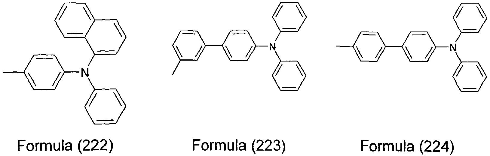


- Depending on the exact structure of the complex according to Formula (1) it is often preferable to have a bridge connecting one or more of the ligands to increase the overall stability of the complex. To facilitate the visualization of the options, Formula (1) can be written as


- Preferred structures having bridged ligands are the metal complexes of the following Formulae (276) to (280):


- Preferably Z represents a single bond or a bridging unit containing 1 to 80 atoms from the third, fourth, fifth and/or sixth main group and/or the transmission metals group (IUPAC group 3 to 12 and 13 to 16) or a 3- to 6-membered homo- or heterocycle which covalently bonds the ligands L to one another or L to L'. The bridging unit Z here may also have an asymmetric structure, i.e. the linking of Z to L or L' needs not to be identical. In a preferred embodiment of the invention, one or more bridging units Z are present and can link one or more of the ligands L and L' either directly from the rings A, B, C or D or from one of the substituents R1, meaning that the ligands have a bidentate or tridentate or polydentate or polypodal character. This results in the formation of macrocyclic ligands or cryptates.
- The bridging unit Z may be neutral, singly, doubly or triply negatively charged or singly, doubly or triply positively charged. Z is preferably neutral or singly negatively positively charged. The charge of Z here is preferably selected so that overall a neutral complex arises.
- If Z is a trivalent group, i.e. bridges two ligands L to L' or two ligands L to one another or one ligand L to L', Z is preferably selected, identical or different on each occurrence, from the group consisting of B, B(R2)-, B(C(R2)2)3, (R2)B(C(R2)2)3 -, B(O)3, (R2)B(O)3 -, B(C(R2)2C(R2)2)3, (R2)B(C(R2)2C(R2)2)3 -, B(C(R2)2O)3, (R2)B(C(R2)2O)3 -, B(OC(R2)2)3, (R2)B(OC(R2)2)3 -, C(R2), CO-, CN(R2)2, (R2)C(C(R2)2)3, (R2)C(O)3, (R2)C(C(R2)2C(R2)2)3, (R2)C(C(R2)2O)3, (R2)C(OC(R2)2)3, (R2)C(Si(R2)2)3, (R2)C(Si(R2)2C(R2)2)3, (R2)C(C(R2)2Si(R2)2)3, (R2)C(Si(R2)2Si(R2)2)3, Si(R2), (R2)Si(C(R2)2)3, (R2)Si(O)3, (R2)Si(C(R2)2C(R2)2)3, (R2)Si(OC(R2)2)3, (R2)Si(C(R2)2O)3, (R2)Si(Si(R2)2)3, (R2)Si(Si(R2)2C(R2)2)3, (R2)Si(C(R2)2Si(R2)2)3, (R2)Si(Si(R2)2Si(R2)2)3, N, NO, N(R2)+, N(C(R2)2)3, (R2)N(C(R2)2)3 +, N(C=O)3, N(C(R2)2C(R2)2)3, (R2)N(C(R2)2C(R2)2)+, P, P(R2)+, PO, PS, PSe, PTe, P(O)3, PO(O)3, P(OC(R2)2)3, PO(OC(R2)2)3, P(C(R2)2)3, P(R2)(C(R2)2)3 +, PO(C(R2)2)3, P(C(R2)2C(R2)2)3, P(R2) (C(R2)2C(R2)2)3 +, PO(C(R2)2C(R2)2)3, S+, S(C(R2)2)3 +, S(C(R2)2C(R2)2)3 +, or a unit of the Formulae (281) to (284),

- If Z is a divalent group, i.e. bridges two ligands L to one another or one ligand L to L', Z is preferably selected, identical or different on each occurrence, from the group consisting of BR2, B(R2)2 -, C(R2)2, C(=O), Si(R2)2, NR2, PR2, P(R2)2 +, P(=O)(R2), P(=S)(R2), AsR2, As(=O)(R2), As(=S)(R2), O, S, Se, or a unit of the Formulae (285) to (294),


- Also preferred are complexes where the ligands L and / or L' themselves contain a bridging unit Z connecting the upper and lower part of the ligand as shown exemplarily in Formulae (295) and (295a).

- The bridging unit Z in Formula (295) can be realized as a covalent or a coordinative bond from ring A to C or D or from ring B to C or D. In case of Formula (295a) the bridging unit Z connects both independent ring systems.
- Some preferred exemplary structures are shown in Formulae (296) to (301). Formulae (302) to (305) are not forming part of the present invention.


- The present invention further relates to a process for the preparation of the metal-complex compounds of the Formula (1). The reaction comprises the following steps 1 to.
-

- Step 1 is preferably carried out in the presence of a palladium catalyst, particularly preferably in the presence of Pd(PPh3)4. To the reaction mixture a base, preferably sodium carbonate, is added, and the reaction is carried out under reflux for up to 30 h. The reaction is carried out in organic solvents, preferably in a mixture of 1,2-dimethoxyethane and ethanol.
-

- Step 2 is preferably carried out by mixing the ligand with a metal chloride in an organic solvent, preferably 2-ethoxyethanol. The mixture is heated to reflux preferably for up to 48 h.
-

- In step 3, the third ligand is added to the chloro-complex solution together with a base, preferably sodium carbonate. The reaction is carried out in an organic solvent, preferably in ethoxyethanol, under reflux for up to 5 h.
- To gain triple heteroleptic complexes the metallation reaction is carried out by mixing Ir(acac)3 and 3 different ligands in an organic solvent, preferably glycerol, under reflux for up to 20 h.
- These processes enable the compounds of the Formula (1) according to the invention to be obtained in high purity, typically greater than 97% (determined by means of 1H-NMR and/or HPLC). Further purification can be easily achieved by recrystallization from a mixture of dichloromethane and methanol.
- The synthetic methods explained here enable the preparation of, inter alia, the compounds of the Formulae (306) to (350) depicted below. Only compounds of the Formulae (307), (309)-(312), (316)-(322), (335), (336), (340)-(342), and (345)-(350) are part of the present invention.


- The complexes of Formula (1) and the preferred embodiments mentioned above can be used as active components in electronic devices. An electronic device is taken to mean a device which comprises an anode, a cathode and at least one layer that comprises at least one organic or organometallic compound. The electronic device according to this invention thus comprises an anode, a cathode and at least one layer which comprises at least one compound of Formula (1) as indicated above. Preferred electronic devices are selected from the group consisting of organic electroluminescent devices (OLEDs, PLEDs), organic integrated circuits (O-ICs), organic field-effect transistors (O-FETs), organic thin-film transistors (O-TFTs), organic light-emitting transistors (O-LETs), organic solar cells (O-SCs), organic optical detectors, organic photoreceptors, organic field-quenching devices (O-FQDs), light-emitting electrochemical cells (LECs or LEECs) or organic laser diodes (O-lasers), comprising, in at least one layer at least one compound of the Formula (1) indicated above. Particular preference is given to organic electroluminescent devices.
- Active components are generally organic or inorganic materials which are introduced between the anode and cathode, for example charge-injection, charge-transport or charge-blocking materials, but in particular emission materials and matrix materials. The compounds according to this invention exhibit particularly good properties as emission material in organic electroluminescent devices. Organic electroluminescent devices are therefore a preferred embodiment of the invention.
- An organic electroluminescent device comprises a cathode, an anode and at least one emitting layer. Apart from these layers, it may also comprise further layers, for example in each case one or more hole-injection layers, hole-transport layers, hole-blocking layers, electron-transport layers, electron-injection layers, exciton-blocking layers, charge-generation layers and/or organic or inorganic p/n junctions. It is likewise possible for interlayers, which have, for example, an exciton-blocking function and/or control the charge balance in the electroluminescent device, to be introduced between two emitting layers. However, it should be pointed out that each of these layers does not necessarily have to be present. The organic electroluminescent device may comprise one or more emitting layers. If more than one emission layer is present, their emission maxima are also preferably different and cover a range from 380 nm to 780 nm, resulting in white emission. Particular preference is given to three-layer systems, where the three layers exhibit blue, green and orange or red emission (for the basic structure see, for example,
WO 2005/011013 ), two layer systems for cheaper two-color whites, or systems which comprise even more than three emitting layers. - In a preferred embodiment of the invention, the organic electroluminescent device comprises the compound of the Formula (1) or the preferred embodiments mentioned above as emitting compound in one or more emitting layers.
- In a particularly preferred embodiment of the invention the organic electroluminescent device has an emission layer processed from solution comprising at least one host material and a material according to Formula (1). The host material can be one or more soluble small molecules and / or one or more polymers. Low-molecular weight additives or polymeric compounds may be added for rheological reasons and / or film formation. Other layers containing active components of the device including additional emission layers may be either evaporated or solution-processed.
- Very particularly preferred is an embodiment in which all layers up to the emission layer are solution-processed. Even more preferred is a simplified device setup that does not require an evaporated organic electron transport layer.
- Also preferred are white luminescent devices made of a light-blue triplet emitter and an orange emitter according to Formula (1) combined in one emission layer in a concentration ratio that renders a two-color white.
- Equally preferred are white luminescent devices with a solution processed emission layer comprising the material according to Formula (1) with an evaporated or solution processed singlet blue layer on top, balanced in concentration and charge distribution to render a two-color-white device.
- If the compound of the Formula (1) is used as emitting compound in an emission layer, it is preferably employed in combination with one or more matrix materials. The mixture of the compound of the Formula (1) and the matrix material comprises between 1 and 99% by weight, preferably between 2 and 50% by weight, particularly preferably between 3 and 40% by weight, in particular between 5 and 30% by weight, of the compound of the formula (1), based on the entire mixture comprising emitter and matrix material. Correspondingly, the mixture comprises between 99 and 1% by weight, preferably between 98 and 50% by weight, particularly preferably between 97 and 60% by weight, in particular between 95 and 70% by weight, of the matrix material, based on the entire mixture comprising emitter and matrix material.
- Suitable matrix materials for the compounds according to the invention are ketones, phosphine oxides, sulfoxides and sulfones, for example in accordance with
WO 2004/013080 ,WO 2004/093207 ,WO 2006/005627 or the applicationDE 102008033943 , triarylamines, carbazole derivatives, such as for example CBP (N,N-biscarbazolylbiphenyl) or the carbazole derivatives disclosed inWO 2005/039246 ,US 2005/0069729 ,JP 2004/ 288381 EP 1205527 orWO 2008/086851 , indolocarbazole derivatives, for example in accordance withWO 2007/063754 orWO 2008/056746 , indenocarbazole derivatives, for example in accordance with the applicationsDE 102009023155 andDE 102009031021 , azacarbazoles, for example in accordance withEP 1617710 ,EP 1617711 ,EP 1731584 ,JP 2005/347160 WO 2007/137725 , silanes, for example in accordance withWO 2005/111172 , azaboroles or boronic esters, for example in accordance withWO 2006/117052 , triazine derivatives, for example in accordance with the applicationDE 102008036982 ,WO 2007/063754 orWO 2008/056746 , zinc complexes, for example in accordance withEP 652273 WO 2009/062578 , diaza- or tetraazasilole derivatives, for example in accordance with the applicationDE 102008056688 , or diazaphosphole derivatives, for example in accordance with applicationDE 102009022858 . - It may also be preferred to employ a plurality of different matrix materials as a mixture, e.g. one or more electron-transporting matrix material and one or more hole-transporting matrix material. A preferred combination is, for example, the use of an aromatic ketone or a triazine with a triarylamine derivative or a carbazole derivative as mixed matrix for the metal complex according to the invention. Preference is likewise also given to mixtures of a hole- or electron-transporting material with a material which is involved in neither hole transport nor electron transport, as disclosed, for example, in
DE 102009014513 . - In a further preferred embodiment of the present invention, the compounds according to the invention can be employed in mixtures with one or more further emitters. Particular preference is given here to a mixture of the compounds according to the invention with one or more phosphorescent emitters where the concentration of each is balanced in such a way that the emitter according to Formula (1) is the one the electroluminescence comes from.
- In a further preferred embodiment of the present invention, the emitter mixtures comprise 3, particularly preferably 2 and very particularly preferably one compound according to the invention.
- In a particularly preferred embodiment of the present invention, the emitter mixtures comprise precisely one of the compounds according to the invention and precisely one further emitter. This further emitter thus acts like a matrix material.
- The compound according to the present invention can, as outlined above, be mixed with further matrix materials. Besides matrix materials the compounds according to the present invention can also be mixed with any other organic functional material that is typically employed in electronic devices. Thus, the present invention also relates to a composition comprising at least one compound according to Formula (1) and at least one organic functional material selected from hole transport material (HTM), hole injection material (HIM), electron transport material (ETM), electron injection material (EIM), hole blocking material (HBM), exciton blocking material (ExBM), host or matrix material, fluorescent emitter, phosphorescent emitter, preferably matrix materials.
- Preferred matrix materials are selected from ketones, phosphinoxides, sulfoxides, sulfones, triarylamines, carbazoles, indolocarbazoles, indenocarbazoles, azacarbazoles, bipolar matrix materials, silanes, azaborolenes, boronesters, triazines, zinc complexes, diaza- or tetraazasiloles or diazaphospholes or mixtures thereof.
- The cathode preferably comprises metals having a low work function, metal alloys or multilayered structures comprising various metals, such as, for example, alkaline-earth metals, alkali metals, main-group metals or lanthanoids (for example Ca, Ba, Mg, Al, In, Mg, Yb, Sm, etc.). Also suitable are alloys of an alkali or alkaline-earth metal and silver, for example an alloy of magnesium and silver. In the case of multilayered structures, further metals which have a relatively high work function, such as, for example, Ag, may also be used in addition to the said metals, in which case combinations of the metals, such as, for example, Ca/Ag or Ba/Ag, are generally used. It may also be preferred to introduce a thin interlayer of a material having a high dielectric constant between a metallic cathode and the organic semiconductor. Suitable for this purpose are, for example, alkali metal or alkaline-earth metal fluorides, but also the corresponding oxides or carbonates (for example LiF, Li2O, BaF2, MgO, NaF, CsF, Cs2CO3, etc.). The layer thickness of this layer is preferably between 0.5 and 5 nm.
- The anode preferably comprises materials having a high work function. The anode preferably has a work function of greater than 4.5 eV vs. vacuum. Suitable for this purpose are on the one hand metals having a high redox potential, such as, for example, Ag, Pt or Au. On the other hand, metal/metal oxide electrodes (for example Al/Ni/NiOx, Al/PtOx) may also be preferred. For some applications, at least one of the electrodes must be transparent in order to enable either irradiation of the organic material (O-SCs) or the outcoupling of light (OLEDs/PLEDs, O-lasers). A preferred structure uses a transparent anode. Preferred anode materials here are conductive mixed metal oxides. Particular preference is given to indium tin oxide (ITO) or indium zinc oxide (IZO). Preference is furthermore given to conductive doped organic materials, in particular conductive doped polymers.
- In general, all materials as used for the layers in accordance with the prior art can be used in the further layers, and the person skilled in the art will be able to combine each of these materials with the materials according to the invention in an electronic device without inventive step.
- The device is correspondingly (depending on the application) structured, provided with contacts and finally hermetically sealed, since the lifetime of devices of this type is drastically shortened in the presence of water and/or air.
- Preference is furthermore given to an organic electroluminescent device, characterised in that one or more layers are applied by means of a sublimation process, in which the materials are vapour-deposited in vacuum sublimation units at an initial pressure of usually less than 10-5 mbar, preferably less than 10-6 mbar. It is also possible for the initial pressure to be even lower, for example less than 10-7 mbar.
- Preference is likewise given to an organic electroluminescent device, characterised in that one or more layers are applied by means of OVPD (organic vapour phase deposition) or with the aid of carrier-gas sublimation, in which the materials are applied at a pressure between 10-5 mbar and 1 bar. A special case of this process is the OVJP (organic vapour jet printing) process, in which the materials are applied directly through a nozzle and thus structured (for example M. S. Arnold et al., Appl. Phys. Lett. 2008, 92, 053301).
- Preference is furthermore given to an organic electroluminescent device, characterised in that one or more layers are produced from solution, such as, for example, by spin coating, or by means of any desired printing process, such as, for example, screen printing, flexographic printing or offset printing, but particularly preferably LITI (light induced thermal imaging, thermal transfer printing) or ink-jet printing. Since the compounds of the Formula (1) according to the invention have very good solubility in organic solvents, they are particularly suitable for processing from solution.
- The organic electroluminescent device can also be produced as a hybrid system by applying one or more layers from solution and applying one or more other layers by vapour deposition. Thus, for example, it is possible to apply an emitting layer comprising a compound of the Formula (1) and a matrix material from solution and to apply a hole-blocking layer and/or an electron-transport layer on top by vacuum vapour deposition.
- These processes are generally known to the person skilled in the art and can be applied by him without problems to organic electroluminescent devices comprising compounds of the Formula (1) or the preferred embodiments mentioned above.
- For processing from solution, solutions or formulations of the compounds of the Formula (1) are necessary. It may also be preferred to use mixtures of two or more solvents. Suitable and preferred solvents are, for example, toluene, anisole, o-, m- or p-xylene, methyl benzoate, dimethylanisole, mesitylene, tetralin, veratrol, THF, methyl-THF, THP, chlorobenzene, dioxane, or mixtures of these solvents.
- The present invention therefore furthermore relates to a solution or formulation comprising at least one compound of the Formula (1) and one or more solvents, in particular organic solvents. The way in which solutions of this type can be prepared is known to the person skilled in the art and is described, for example, in
WO 02/072714 WO 03/019694 - Some of the basic areas of application here are display or illumination technologies. Due to the potential simplicity of the devices, large area and thus very cheap device fabrication by any kind of printing method or roll-to-roll-processing is possible. One further preferred application is therefore the use of the materials according to Formula (1) in flexible devices which are then particularly well suited for phototherapy.
- The present invention therefore furthermore relates to the use of the compounds or compositions according to the invention and devices comprising the compounds for the treatment, prophylaxis and diagnosis of diseases. The present invention furthermore relates to the use of the compounds or compositions according to the invention and devices comprising the compounds for the treatment and prophylaxis of cosmetic conditions.
- The present invention furthermore relates to the use of the compounds or compositions according to the invention for the production of devices for the therapy, prophylaxis and/or diagnosis of therapeutic diseases and/or for cosmetic applications.
- Phototherapy or light therapy is used in many medical and/or cosmetic areas. The compounds or compositions according to the invention and the devices comprising them can therefore be employed for the therapy and/or prophylaxis and/or diagnosis of all diseases and/or in any cosmetic applications for which the person skilled in the art considers the use of phototherapy. Besides irradiation, the term phototherapy also includes photodynamic therapy (PDT) and disinfection and sterilisation in general. Phototherapy or light therapy can be used for the treatment of not only humans or animals, but also any other type of living or non-living materials. These include, for example, fungi, bacteria, microbes, viruses, eukaryotes, prokaryonts, foods, drinks, water and drinking water.
- The term phototherapy also includes any type of combination of light therapy and other types of therapy, such as, for example, treatment with active compounds. Many light therapies have the aim of irradiating or treating exterior parts of an object, such as the skin of humans and animals, wounds, mucous membranes, the eye, hair, nails, the nail bed, gums and the tongue. The treatment or irradiation according to the invention can in addition also be carried out inside an object in order, for example, to treat internal organs (heart, lung, etc.) or blood vessels or the breast.
- The therapeutic and/or cosmetic areas of application according to the invention are preferably selected from the group of skin diseases and skin-associated diseases or changes or conditions, such as, for example, psoriasis, skin ageing, skin wrinkling, skin rejuvenation, enlarged skin pores, cellulite, oily/greasy skin, folliculitis, actinic keratosis, precancerous actinic keratosis, skin lesions, sun-damaged and sun-stressed skin, crows' feet, skin ulcers, acne, acne rosacea, scars caused by acne, acne bacteria, photomodulation of greasy/oily sebaceous glands and their surrounding tissue, jaundice, jaundice of the newborn, vitiligo, skin cancer, skin tumours, Crigler-Najjar, dermatitis, atopic dermatitis, diabetic skin ulcers and desensitisation of the skin.
- Particular preference is given for the purposes of the invention to the treatment and/or prophylaxis of psoriasis, acne, cellulite, skin wrinkling, skin ageing, jaundice and vitiligo.
- Very particular preference is given to the use of the light emitting devices comprising the compounds or compositions according to the present invention to reduce or prevent skin ageing and the formation of skin wrinkles. The treatment of skin with orange light in these cases is particularly beneficial.
- Further areas of application according to the invention for the compounds or compositions and/or devices comprising them are selected from the group of inflammatory diseases, rheumatoid arthritis, pain therapy, treatment of wounds, neurological diseases and conditions, oedema, Paget's disease, primary and metastasising tumours, connective-tissue diseases or changes, changes in the collagen, fibroblasts and cell level originating from fibroblasts in tissues of mammals, irradiation of the retina, neovascular and hypertrophic diseases, allergic reactions, irradiation of the respiratory tract, sweating, ocular neovascular diseases, viral infections, particularly infections caused by herpes simplex or HPV (human papillomaviruses) for the treatment of warts and genital warts.
- Particular preference is given for the purposes of the invention to the treatment and/or prophylaxis of rheumatoid arthritis, viral infections and pain.
- Further areas of application according to the invention for the compounds or compositions and/or devices comprising them are selected from winter depression, sleeping sickness, irradiation for improving the mood, the reduction in pain, particularly muscular pain caused by, for example, tension or joint pain, elimination of the stiffness of joints and the whitening of the teeth (bleaching).
- Further areas of application according to the invention for the compounds or compositions and/or devices comprising them are selected from the group of disinfections. The compounds or compositions according to the invention and/or the devices can be used for the treatment of any type of objects (non-living materials) or subjects (living materials such as, for example, humans and animals) for the purposes of disinfection. This includes, for example, the disinfection of wounds, the reduction in bacteria, the disinfection of surgical instruments or other articles, the disinfection of foods, of liquids, in particular water, drinking water and other drinks, the disinfection of mucous membranes and gums and teeth. Disinfection here is taken to mean the reduction in the living microbiological causative agents of undesired effects, such as bacteria and germs.
- For the purposes of phototherapy, devices comprising the compounds or compositions according to the invention preferably emit light having a wavelength between 300 and 1250 nm, particularly preferably between 440 and 1000 nm, particularly preferably between 500 and 850 nm and very particularly preferably between 560 and 620 nm.
- In a particularly preferred embodiment of the present invention, the compounds or compositions according to the invention are employed in an organic light-emitting diode (OLED) or an organic light-emitting electrochemical cell (OLEC) for the purposes of phototherapy. Both the OLED and the OLEC can have a planar or fibre-like structure having any desired cross section (for example round, oval, polygonal, square) with a single- or multilayered structure. These OLECs and/or OLEDs can be installed in other devices which comprise further mechanical, adhesive and/or electronic elements (for example battery and/or control unit for adjustment of the irradiation times, intensities and wavelengths). These devices comprising the OLECs and/or OLEDs according to the invention are preferably selected from the group comprising plasters, pads, tapes, bandages, cuffs, blankets, caps, sleeping bags, textiles and stents.
- The use of OLED- or OLEC-devices for therapeutic and/or cosmetic purposes is particularly advantageous compared to the prior art since homogeneous irradiation with lower intensity is possible virtually anywhere and anytime. The irradiation can be carried out on an in- or outpatient basis or, especially for cosmetic purposes, even by the customers themselves without initiation by medical or cosmetic specialists. Thus, for example, bandages and plasters can be worn under clothing, so that irradiation is also possible during working hours, in leisure time or during sleep. Complex inpatient/outpatient treatments can in many cases be avoided or their frequency reduced. The devices according to the invention may be intended for re-use or be disposable articles, which can be disposed of after use once, twice or three times.
- Further advantages over the prior art are, for example, lower evolution of heat and emotional aspects. Thus, newborn being treated owing to jaundice typically have to be irradiated blindfolded in an incubator without physical contact with the parents, which represents an emotional stress situation for parents and newborn. With the aid of a blanket according to the invention comprising the OLEDs and/or OLECs according to the invention, the emotional stress can be reduced significantly. In addition, better temperature control of the child is possible due to reduced heat production of the devices according to the invention compared with conventional irradiation equipment.
- The new materials and electronic devices according to the invention, in particular organic electroluminescent devices, are distinguished by the following surprising advantages over the prior art:
- 1. Synthesis with high yield and purification of the compounds according to the present invention is easy, even on large scale. This makes upscaling straightforward and the materials suited for mass production of devices.
- 2. The compounds of the Formula (1) have very good solubility in a high number of common organic solvents and are therefore very highly suitable for processing from solution. This makes them ideally suited for applications that require low production costs, such as illumination and signage devices, and for roll-to-roll-processed devices on flexible substrates.
- 3. The compounds of Formula (1) and the electronic devices comprising them show improved stability and improved shelf life compared to similar compounds of the prior art.
- 4. Organic electroluminescent devices comprising compounds of the Formula (1) as emitting materials show excellent efficiencies and lifetimes. Even very simple devices have efficiencies and lifetimes sufficient for monochrome illumination and signage applications.
- 5. The emission color of the compounds according to Formula (1) is beneficial for a number of different applications, e.g. for the treatment or prevention of skin issues in phototherapeutic devices or for low cost two-color white devices for lighting applications.
- These above-mentioned advantages are not accompanied by an impairment in the other electronic properties.
- It should be pointed out that variations of the embodiments described in the present invention fall within the scope of this invention. Each feature disclosed in the present invention can, unless explicitly excluded, be replaced by alternative features which serve the same, an equivalent or a similar purpose. Thus, each feature disclosed in the present invention should, unless stated otherwise, be regarded as an example of a generic series or as an equivalent or similar feature.
- All features of the present invention can be combined with one another in any way, unless certain features and/or steps are mutually exclusive. This applies, in particular, to preferred features of the present invention. Equally, features of non-essential combinations can be used separately (and not in combination).
- It should furthermore be pointed out that many of the features, and in particular those of the preferred embodiments of the present invention, should be regarded as inventive themselves and not merely as part of the embodiments of the present invention. Independent protection may be granted for these features in addition or as an alternative to each invention claimed at present.
- The teaching regarding technical action disclosed with the present invention can be abstracted and combined with other examples.
- The invention is explained in greater detail by the following examples without wishing it to be restricted thereby.
-
Materials (Acronyms) Structure Name (acronym) 
2-(dibenzo[b,d]furan-4-yl)quinoline (dbfqH) 
2-(dibenzo[b,d]furan-4-yl)-4-methylquinoline (dbfmqH) 
2-dibenzothiophene-4-yl-quinoline (dbtqH) 
(2-(3-(trifluoromethyl)-1H-pyrazol-5-yl)pyridine) (fppzH) (not forming part of the present invention) 
2-(3-(trifluoromethyl)-1H-1,2,4-triazol-5-yl)pyridine (fptzH) 
2-(3-methyl-1H-pyrazol-5-yl)pyridine (mppzH) (not forming part of the present invention) 
2-(3-(tert-butyl)-1H-pyrazol-5-yl)pyridine (bppzH) (not forming part of the present invention) 
2-(3-(perfluorobutyl)-1H-pyrazol-5-yl)pyridine (hppzH) (not forming part of the present invention) 
2-(3-(perfluorobutyl)-1H-1,2,4-triazol-5-yl)pyridine (hptzH) 
2-(3-phenyl-1H-1,2,4-triazol-5-yl)pyridine (pptzH) 
2-(3-methyl-1H-1,2,4-triazol-5-yl)pyridine (mptzH) 
2-(3-tert-butyl)-1H-1,2,4-triazol-5-yl)pyridine (tptzH) 
2-(3-trifluoromethyl)-1H-[1,2,4]triazol-4-yl)-4-methyl-5-pyridin iodide (ftmpiH) 
picolinic acid (pic) - Chemical syntheses of the ligands bppzH and mppzH are well known to one skilled in the art. They can be prepared according to Yu, Wei-Shan et al., JACS, 125(36), 10800-10801; 2003.
- Chemical syntheses of the ligands pptzH and mptzH are well known to one skilled in the art. They can be prepared according to Orselli, Enrico et al, Inorg. Chem, 46(26), 11082-11093; 2007.


- The compounds V1, V2, V4, SSM-1, SSM-2, SSM-3, ET-1 and ET-2 are well known from the prior art. As an example, the compounds V1, V2, V4, SSM-1, SSM-2, SSM-3 and ET-1 have been disclosed in
WO 2005/033244 ,WO 2004/026886 ,JP 2012/77069 WO 2011/137922 ,WO 2012/048778 ,WO 2011/032626 andWO 2010/072300 , respectively. Compound ET-2 can be purchased from ABCR GmbH & Co. KG, Karlsruhe. Compound V3 ([(dbfq)2Ir(pic)]) is a complex showing deep red light emission. V3 can be prepared according to the procedure as outlined in Example 8, wherein pic (30 mg, 0.24 mmol) is used instead of fppzH. V4 can be obtained with 74% yield. -

- To a mixture of 2-chloroisoquinoline (1.73 g, 10.5 mmol) and Pd(PPh3)4 (403 mg, 0.349 mmol) in 1,2-dimethoxyethane (50 mL) a solution of dibenzofuran-4-ylboronic acid (2.30 g, 10.9 mmol) in degassed ethanol (50 mL) is added, followed by addition of 2.6 M aqueous sodium carbonate solution (50 mL). Then, the mixture is heated under reflux for 19 h under inert atmosphere. After cooling, ethyl acetate (50 mL) and water (100 mL) are added, and the insoluble materials are removed by filtration. The filtrate is treated with a standard aqueous workup. The solvent is removed and the residue is purified by column chromatography to render a yellow solid. Recrystallization from chloroform/hexane yields a white crystalline solid of the titled compound dbfqH in 84% yield (2.62 g, 8.87 mmol).
- In analogy to the preparation of (dbfqH) according to Example 1 the Suzuki coupling reaction can be used to parepare a variety of similar compounds such as compounds L1 to L44. The general preparation method is as follows:
To a mixture of the halogen-compound (10.5 mmol; educt 2) and Pd(PPh3)4 (0.35 mmol, 1/30 eq.) in 1,2-dimethoxyethane (50 mL) a solution of boronic acid (11 mmol; educt 1) in degassed ethanol (50 mL) is added, followed by addition of 2.6 M aqueous sodium carbonate solution (50 mL). Then, the mixture is heated under reflux for 20 h under inert atmosphere. After cooling, ethyl acetate (50 mL) and water (100 mL) are added, and the insoluble materials are removed by filtration. The filtrate is treated with a standard aqueous workup. The solvent is removed and the residue is purified by column chromatography. Recrystallization from chloroform/hexane yields a white crystalline solid of the compound in abou 65 to 90% yield. - The following ligands can be prepared according to the method provided herein:
Educt 1 Educt 2 Product Yield 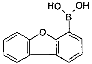


84% CAS 100124-06-9 CAS 612-62-4 L1 


78% CAS 100124-06-9 CAS 634-47-9 L2 


81% CAS 100124-06-9 CAS 68236-03-3 L3 


73% CAS 100124-06-9 CAS 68236-03-3 L4 


69% CAS 395087-89-5 CAS 612-62-4 L5 


81% CAS 395087-89-5 CAS 634-47-9 L6 


86% CAS 395087-89-5 CAS 68236-03-3 L7 


74% CAS 395087-89-5 CAS 68236-03-3 L8 


86% CAS 402936-15-6 CAS 612-62-4 L9 


71% CAS 402936-15-6 CAS 634-47-9 L10 


83% CAS 402936-15-6 CAS 68236-03-3 L11 


82% CAS 402936-15-6 CAS 68236-03-3 L12 


78% CAS 162607-19-4 CAS 612-62-4 L13 


79% CAS 162607-19-4 CAS 634-47-9 L14 


85% CAS 162607-19-4 CAS 68236-03-3 L15 


89% CAS 162607-19-4 CAS 68236-03-3 L16 


76% CAS 108847-20-7 CAS 612-62-4 L17 


90% CAS 108847-20-7 CAS 634-47-9 L18 


95% CAS 108847-20-7 CAS 68236-03-3 L19 


86% CAS 108847-20-7 CAS 68236-03-3 L20 


79% CAS 108847-24-1 CAS 612-62-4 L21 


76% CAS 108847-24-1 CAS 634-47-9 L22 


84% CAS 108847-24-1 CAS 68236-03-3 L23 


91% CAS 108847-24-1 CAS 68236-03-3 L24 


83% CAS 668983-97-9 CAS 612-62-4 L25 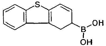


77% CAS 668983-97-9 CAS 634-47-9 L26 


76% CAS 668983-97-9 CAS 68236-03-3 L27 


85% CAS 668983-97-9 CAS 68236-03-3 L28 


71% CAS 1245943-60-5 CAS 612-62-4 L29 


80% CAS 1245943-60-5 CAS 634-47-9 L30 


83% CAS 1245943-60-5 CAS 68236-03-3 L31 


78% CAS 1245943-60-5 CAS 68236-03-3 L32 


72% CAS 1039761-02-8 CAS 612-62-4 L33 


86% CAS 1039761-02-8 CAS 634-47-9 L34 


81% CAS 1039761-02-8 CAS 68236-03-3 L35 


83% CAS 1039761-02-8 CAS 68236-03-3 L36 


75% CAS 886232-59-3 CAS 612-62-4 L37 


92% CAS 886232-59-3 CAS 634-47-9 L38 


77% CAS 886232-59-3 CAS 68236-03-3 L39 


73% CAS 886232-59-3 CAS 68236-03-3 L40 


79% CAS 1370555-65-9 CAS 612-62-4 L41 


70% CAS 1370555-65-9 CAS 634-47-9 L42 


91% CAS 1370555-65-9 CAS 68236-03-3 L43 


85% CAS 1370555-65-9 CAS 68236-03-3 L44 -

- Concentrations used in the reaction are provided for both fppzH and hppzH in the following description.
- NaOEt (in case of fppzH: 1.82 g, 26.8 mmol; in case of hppzH: 1.23 g, 18.0 mmol) is dispersed in 50 mL of dry tetrahydrofuran (THF). To this solution either ethyl trifluoroacetate (3.2 mL, 26.8 mmol) for fppzH or nonafluoropentanoic acid ethyl ester (3.0 ml, 15.1 mmol) for hppzH is added slowly at 0°C. The mixture is stirred for 2 h followed by the addition of 2-acetylpyridine (in case of fppzH: 2.0 mL, 17.9 mmol; in case of hppzH: 1.87 mL, 16.7 mmol) at 0°C. The reaction is then heated to 50°C for 4 h. Removal of the solvent renders a brown oily residue, which is dispersed in de-ionized water (50 mL). The mixture is neutralized with 2 N HCl(aq) (pH = 4), followed by extraction with ethyl acetate (3 × 50 mL). The combined organic residue is dried over anhydrous Na2SO4. After filtration, a brown oil, the diketone, is obtained which is used without further purification. It is dissolved in 50 mL EtOH and treated with hydrazine monohydrate (in case of fppzH: 10 eq; in case of hppzH: 5 eq). The mixture is refluxed for 12 h. After cooling to room temperature, evaporation of the solvent at reduced pressure renders a brown residue, which is then dissolved in ethyl acetate. The organic phase is washed with water (20 mL × 3), dried over Na2SO4, and then filtered. Removal of ethyl acetate gives a pale-yellow solid. Finally the solid is recrystallized from CH2Cl2 / hexane. Compound fppzH is obtained with 62% yield (2.4 g, 11 mmol). Compound hppzH is obtained in 68% yield (3.7 g, 10.2 mmol).
-

- A mixture of 2-cyanopyridine (3.15 g, 30.3 mmol) and NaOCH3 (0.16 g, 3 mmol) is prepared in 10 mL ethanol and stirred at RT for 4 h under inert atmosphere. After 4 h, NH4Cl (1.81 g,33.8 mmol) is added to the solution. The mixture is refluxed for 6 hours, cooled down and filtered to remove excess salt. Ethanol is removed and a white solid of 2-pyridinecarboximidamidehydrochloride (3.99 g, 25.2 mmol) is obtained.
- A solution of ethyl trifluoroacetate (3.52 g, 24.77 mmol) and hydrazine monohydrate (1.14 mL, 23.50 mmol) in 50 mL THF is refluxed for 1 h. Upon cooling to room temperature, 2-pyridinecarboximidamidehydrochloride (3.99 g, 25.32 mmol) and NaOH (1.01 g, 25.32 mmol) are added to the solution. The mixture is refluxed for 6 h and cooled to room temperature. Afterwards a white solid is obtained by extraction with ethyl acetate.. The product is purified via column chromatography and obtained with 56% yield (2.82 g, 13.16 mmol).
- A solution of nonafluoropentanoic acid ethyl ester (4.35 g, 14.9 mmol) and hydrazine monohydrate (0.73 mL, 15.8 mmol) in 50 mL THF is refluxed for 1 h. Upon cooling to room temperature, 2-pyridinecarboximidamide hydrochloride (2.49 g, 15.7 mmol) and NaOH (0.63 g, 15.8 mmol) are added to the solution. The mixture is refluxed for 6 h and cooled to room temperature. After the reaction is finished, a white solid is obtained by ethyl acetate extraction. The product is purified via column chromatography and is obtained in 62% yield (3.36 g, 9.23 mmol).
-

- A mixture of 2-cyanopyridine (3.15 g, 30.3 mmol) and NaOCH3 (0.16 g, 3 mmol) is prepared in 10 mL ethanol and stirred at RT for 4 h under inert atmosphere. After 4 h, NH4Cl (1.81 g, 33.8 mmol) is added to the solution. The mixture is refluxed for 6 h, cooled down and filtered to remove excess salt. Ethanol is removed and a white solid of 2-pyridinecarboximidamide-hydrochloride (3.99 g, 25.2 mmol) is obtained.
- A solution of pivalic acid chloride(3.54 g, 29.3 mmol) in 10 mL CH2Cl2 is added drop wise to 2-pyridinecarboximidamidehydrochloride (4 g, 29.3 mmol) and Na2CO3 (3.1 g, 29.3 mmol) in 100 mL H2O. The reaction mixture is stirred at RT for 2 h, yielding a white precipitate. The precipitate is filtered, and the solid washed with water and ethanol. The solid then is suspended in 5 mL of ethylene glycol and heated to 200°C for 2 h, yielding a pale yellow solution. Upon cooling to room temperature, a white solid is formed, filtered of and washed with de-ionized water. The solid is dried under vacuum and used without further purification (3.2 g, 15.8 mmol, 53.8%).
-

- A mixture of ftptz (500 mg, 3.12 mmol) and methyl iodide (1 ml, 2.27 g, 16 mmol) is refluxed for 8 h, then anhydrous diethylether (100 ml) is added and the precipitate is filtered off. Recrystallisation from acetone renders a colorless product (424 mg, 1.40 mmol, 45% yield).
-

- A solution of dbfqH (0.34 g, 1.15 mmol) and IrCl3•3H2O (205 mg, 0.585 mmol) in 2-ethoxyethanol (15 mL) is refluxed for 24 h. After cooling, water (50 mL) is added and the precipitate is collected by filtration. The solid is washed with ethanol (20 mL) and hexane (20 mL) to obtain the titled compound (I) as a red powder (0.36 g, 0.23 mmol, 78% yield). This material is used without further purification.
- In analogy to the preparation of (dbfq)2Ir(µ-Cl)2Ir(dbfq)2 (I) according to Example 7 further dimers can be produced. The general preparation method is as follows:
A solution of ligand (1 mmol) and IrCl3•3H2O (180 mg, 0.513 mmol) in 2-ethoxyethanol (15 mL) is refluxed for 24 h. After cooling, water (50 mL) is added and the precipitate is collected by filtration. The solid is washed with ethanol (20 mL) and hexane (20 mL) to obtain the chloro-bridged dimer as a powder. This material is used without further purification.


-

- A mixture of (dbfq)2Ir(µ-Cl)2Ir(dbfq)2 (I) (200 mg, 0.122 mmol), fppzH (53 mg, 0.248 mmol) and Na2CO3 (120 mg, 1.13 mmol) in ethoxyethanol (10 mL) is heated at 130°C for 2 h under inert atmosphere. After cooling, the reaction mixture is poured into water (50 mL) and the precipitate is collected by filtration. The solid is purified via column chromatography using CH2Cl2 as eluent. Further purification is carried out by recrystallization from CH2Cl2 /methanol to obtain compound (III) as a red powder (180 mg, 0.18 mmol, 74% yield).
-

- A mixture of (dbfq)2Ir(µ-Cl)2Ir(dbfq)2 (I) (200 mg, 0.122 mmol), ftmpiH (89 mg, 0.250 mmol) and Na2CO3 (120 mg, 1.13 mmol) in ethoxyethanol (10 mL) is heated to 130°C for 2 h in an inert atmosphere. After cooling, the reaction mixture is poured into water (50 mL) and the aqueous phase is extracted with dichloromethane. After removing the solvent, the product is purified via column chromatography using CH2Cl2 as eluent. Further purification is carried out by recrystallization to obtain compound (XIII) as a red powder (185 mg, 0.17 mmol, 70% yield).
- In analogy to the preparation according to Example 10 further complexes can be produced. The general preparation method is as follows:
A mixture of the chloro-bridged dimer (Ir(Lxx)2Cl)2 (0.177 mmol) wherein Lxx is defined as being one of the ligands L1 to L44, the third ligand (fppz, fptz, mppz, bppz, hppz, hptz, pptz, mptz, tptz, or ftmpi) (0.365 mmol) and Na2CO3 (0.85 mmol) are solved in ethoxyethanol (10 mL) and the reaction mixture is heated at 130°C for 5 h in an inert atmosphere. After cooling, the reaction mixture is poured into water (50 mL) and the precipitate is collected by filtration. The solid is purified via column chromatography using CH2Cl2 as eluent. Further purification is carried out by recrystallization from CH2Cl2 /methanol to obtain the compound as a red powder. - The compounds given in the following table can be made according to the general procedure out of the chloro-bridged-dimers (Ir(L1)2Cl)2 to (Ir(L44)-2Cl)2 and the third ligands ligand (fppz, fptz, mppz, bppz, hppz, hptz, pptz, mptz, tptz, or ftmpi). The over-all yield for each reaction is between 43% and 78%. The compounds given in the following table having the third ligand selected from fppz, mppz, bppz and hppz are not forming part of the present invention.


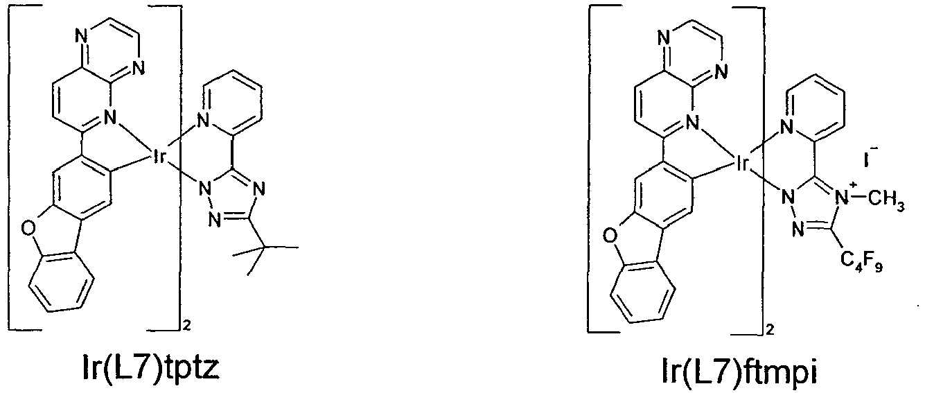


-

- Compound (XIII) (500 mg, 0.46 mmol) is dissolved in a mixture of CH2Cl2 and MeOH (2:1, 30 mL) and KPF6 in MeOH (5 mL) is added. After stirring for 12 h at room temperature, the solvent is removed in vacuu and the residue is washed with de-ionized water (50 mL). Recrystallization yields in a red powder of compound (XIV) (395 mg, 0,36 mmol, 78% yield).
- In analogy to the preparation according to Example 12 further complexes can be produced. The general preparation method is as follows: Compound (Ir(Lxx)ftmpi) (0.5 mmol) is dissolved in a mixture of CH2Cl2 and MeOH (2:1, 30 mL) and KPF6 in MeOH (5 mL) is added, wherein Lxx is defined as being one of the ligands L1 to L44,. After stirring for 12 h at room temperature, the solvent is removed in vacuu and the residue is washed with de-ionized water (50 mL). Recrystallization yields in a powder of the hexafluorophosphate compound (Ir(Lxx)ftmpp).
- The following table shows all ftmpi-based emitter compounds which can be converted to the ftmpp compounds according to this procedure with yields between 67% to 83%.


- Organic light emitting diodes (OLEDs) comprising materials according to this invention are made according to processes that are well known to one skilled in the art and that have been described in the literature many times (for example in
WO 2004/037887 A2 for OLEDs made from solution, andWO 2004/058911 for OLEDs made by thermal evaporation). - Emitters from the present invention are particularly well suited for OLEDs made from solution. A typical OLED device has the following layered structure: Ba/Al cathode (3 nm/100 nm)/EML (80 nm; 6-7 wt.-% emitter)/Interlayer (20 nm; HIL-012)/PEDOT (80 nm; Clevios P 4083 Al)/ITO, wherein EML represents the emissive layer.ITO-coated glass substrates are purchased from Technoprint, the cathode is deposited by vapour-deposition through an evaporation mask.
- The substrates are cleaned with de-ionised water and a detergent (Deconex 15 PF) in a clean room and then activated by UV/ozone plasma treatment. An 80 nm PEDOT layer (PEDOT is a polythiophene derivative (Clevios P 4083 Al) from H. C. Starck, Goslar, which is supplied as an aqueous dispersion) is then applied by spin coating, likewise in a clean room. The required spin rate depends on the degree of dilution and the specific spin-coater geometry (typical for 80 nm: 4500 rpm). In order to remove residual water from the layer, the substrates are dried by heating on a hotplate at 180°C for 10 minutes. The substrates are transferred into a glove box and all subsequent coating and annealing steps are carried out in an inert-gas atmosphere (nitrogen or argon). A 20 nm film of an interlayer (typically a hole-dominated polymer, here HIL-012 from Merck) is spin-coated onto the substrate from a 5 g/L toluene solution and heated for 60 min. at 180°C. A particular advantage of some of the devices shown here is that even the interlayer can be omitted and thus very simple devices can be made. In the device setup 80 nm of an EML are applied from toluene solution. The concentrations depend on the specific composition of the EML: For EMLs that contain polymeric host materials, the concentration is 10 g/L, for EMLs based on soluble small molecules 18 to 20 g/L. The solvent for spin-coating is toluene. After the film is applied, the layers are annealed at 180°C for 10 minutes. The Ba/AI cathode is then vapour-deposited, (high-purity metals from Aldrich, particularly barium 99.99% (Order No. 474711); typical vacuum level 5 x 10⁻⁶ mbar). Alternatively, an organic electron transport layer (ETL) may be vapour-deposited between the solution processed EML and the cathode which then typically does not contain a Ba-layer. Finally, the device is encapsulated in order to protect the layers from air and atmospheric moisture.
- Devices are characterized in holders manufactured specifically for the substrate size. Electrical contact is made with spring contacts. A photodiode with eye response filter is placed directly on the measurement holder in order to exclude influences from extraneous light. Voltages are typically increased from 0 to max. 12 V in 0.2 V steps and reduced again. For each voltage, the current through the device and the photocurrent through the photodiode are measured. This way, the IUL data of the test devices are obtained. Important parameters are the efficiency and required voltage for 1000 cd/m2 as well as the external quantum efficiency (EQE, in %). To determine the colour and the precise electroluminescence spectrum of the test devices, the voltage required for 1000 cd/m2 is applied again and the photodiode is replaced by a cover that connects the sample holder with an Ocean Optics spectrometer via an optical fibre. The colour coordinates (CIE: Commission Internationale de l'Éclairage, standard observer from 1931) can be derived from the measured spectrum.
- Device lifetimes are measured in a separate setup, but in a very similar way. Based on the characterization data, voltage and current are provided to reach an initial luminance of 2000 to 6000 cd/m2 (chosen based on the initial efficiency of the specific device). Then the current is kept constant, which typically leads to an increase in voltage while the device is driven. Here, the lifetimes are determined as T50, the time when the initial luminance has degraded to 50% of the initial value. In order to compare lifetimes for devices with different starting brightnesses, the lifetimes are extrapolated to a starting brightness of 1000 cd/m2 with an extrapolation factor of 1.9 for devices with interlayer and 1.625 for devices without.
- The examples of solution processed devices with polymer matrices are mainly intended for cheap monochrome applications. They need sufficient lifetime, but mainly good efficiency and "unusual" (not display-type) colour. Solution processed devices with soluble small molecules can still be used for these applications, but are a little more demanding in terms of processing. They will therefore more likely be used in high-end applications where lifetime is also very important.
- 80 nm of the EML are spin-coated directly onto PEDOT. The concentration of the emitters is 7% by weight based on the polymer matrix P1. The overall concentration is 10 g/L, i.e. 9.3 g/L P1 and 0.7 g/L emitter, the spin-rate is ∼ 1200 rpm. The matrix of choice for these simple devices is P1, the polymerization of the monomers is carried out according to
WO 2005/040302 :
- The results are summarized in Table 1. The new emitters have a reasonable lifetime even in these simple and, thus, cheap devices. The colour is more orange, as intended, the efficiencies are very high for such a simple setup. The compounds given in Table 1 having the third ligand selected from fppz, mppz, bppz and hppz are not forming part of the present invention.
Table 1: Device Emitter Host ETL / Cathode Eff.* / (cd/A) EQE* U* / V CIE* LT50* / h 1 V1 P1 Ba / Al 10.4 6.4% 4.2 0.63 / 0.37 840 2 (Ir(L1)fppz) P1 Ba / Al 11.4 6.0% 5.1 0.61 / 0.39 460 3 (Ir(L1)fptz) P1 Ba / Al 10.8 5.2% 4.9 0.59/ 0.41 320 4 (Ir(L3)tptz) P1 Ba / Al 10.1 6.1 4.9 0.59/ 0.38 530 5 (Ir(L5)bppz) P1 Ba/ Al 10.5 5.9 5.0 0.58/ 0.39 350 6 (Ir(L6)hppz) P1 Ba / Al 10.9 5.7 4.5 0.62/ 0.35 480 7 (Ir(L9)pptz) P1 Ba / Al 10.8 6.2 4.8 0.61 / 0.37 340 8 (Ir(L11)fptz) P1 Ba / Al 11.0 6.1 4.7 0.59/ 0.39 510 9 (Ir(L14)mptz) P1 Ba / Al 11.3 5.9 5.1 0.61/ 0.38 490 10 (Ir(L16)pptz) P1 Ba / Al 10.6 5.6 4.3 0.61/ 0.36 400 11 (Ir(L19)pptz) P1 Ba / Al 10.3 5.2 4.4 0.60/ 0.37 420 12 (Ir(L22)hppz) P1 Ba / Al 11.1 5.3 5.1 0.58/ 0.37 500 13 (Ir(L26)mptz) P1 Ba / Al 9.8 5.9 5.3 0.59/ 0.35 390 14 (Ir(L35)bppz) P1 Ba / Al 10.7 5.7 4.8 0.56 / 0.40 450 16 (Ir(L41)pptz) P1 Ba / Al 11.2 6.0 5.1 0.60/ 0.39 380 17 (Ir(L44)mppz) P1 Ba / Al 10.7 5.7 5.0 0.61/ 0.36 430 * all values at 1000 cd/m2 - 80 nm of the EML are spin-coated onto HIL-012. The concentration of the emitters is 7% by weight based on the polymer matrix P2. The overall concentration is 10 g/L, i.e. 9.3 g/L P2 and 0.7 g/L emitter, the spin-rate is ∼ 1200 rpm. The matrix of choice for these devices is P2, the polymerization of the monomers is carried out according to
WO 2005/040302 :
- The results are summarized in Table 2. The compounds given in Table 2 having the third ligand selected from fppz, mppz, bppz and hppz are not forming part of the present invention.
Table 2: Device Interlayer Emitter Host ETL / Cathode Eff.* / (cd/A) EQE* U* / V CIE* LT50* / h 18 HIL-012 V2 P2 Ba / Al 0.70 0.4% 10.1 0.57 / 0.41 NA 19 HIL-012 (Ir(L1)fppz) P2 Ba / Al 9.3 4.7% 6.0 0.60 / 0.39 550 20 HIL-012 (Ir(L1)fptz) P2 Ba / Al 7.3 3.4% 6.2 0.58 / 0.41 450 21 HIL-012 (Ir(L3)tptz) P2 Ba / Al 7.1 4.0 5.9 0.58 / 0.38 737 22 HIL-012 (Ir(L5)bpp z) P2 Ba / Al 7.8 4.4 6.3 0.57 / 0.39 473 23 HIL-012 (Ir(L6)hpp z) P2 Ba / Al 8.6 4.2 5.4 0.61 / 0.35 667 24 HIL-012 (Ir(L9)pptz) P2 Ba / Al 8.3 4.8 5.7 0.60 / 0.37 425 25 HIL-012 (Ir(L11)fptz) P2 Ba / Al 7.7 4.3 5.6 0.58/ 0.39 658 26 HIL-012 (Ir(L14)mptz) P2 Ba / Al 7.4 4.5 6.4 0.60 / 0.38 686 27 HIL-012 (Ir(L16)pptz) P2 Ba / Al 7.9 3.9 5.3 0.60 / 0.36 520 28 HIL-012 (Ir(L19)pptz) P2 Ba / Al 7.9 3.1 5.5 0.59/ 0.37 512 29 HIL-012 (Ir(L22)hppz) P2 Ba / Al 7.4 3.6 6.2 0.57 / 0.37 625 30 HIL-012 (Ir(L26)mptz) P2 Ba / Al 7.4 4.2 6.4 0.58/ 0.35 534 31 HIL-012 (Ir(L35)bppz) P2 Ba / Al 9.3 3.8 5.7 0.55/ 0.40 599 33 HIL-012 (Ir(L41)pptz) P2 Ba / Al 7.9 4.4 6.3 0.59 / 0.39 532 34 HIL-012 (Ir(L44)mppz) P2 Ba / Al 7.1 4.3 6.1 0.60 / 0.36 563 * all values at 1000 cd/m2 - 80 nm of the EML are spin-coated onto HIL-012. The soluble small molecule matrix consists of 30 wt.-% SSM1, 42 wt.-% SSM2 and 22 wt.-% SSM3 (= composition 1). The emitter concentration is 6 wt.-%. The overall concentration is 18 g/L, the spin-rates are between 650 and 1300 rpm. The results are summarized in Table 3. The compounds given in Table 3 having the third ligand selected from fppz, mppz, bppz and hppz are not forming part of the present invention.
Table 3: Device Interlayer Emitter Host ETL / Cathode Eff.* / (cd/A) EQE* U* / V CIE* LT50* / h 35 HIL-012 V1 Com p.1 Ba / Al 11.0 7.5% 7.3 0.63 / 0.37 8000 36 HIL-012 V2 Com p.1 Ba / Al 7.3 3.9% 10.1 0.58 / 0.41 330 37 HIL-012 V3 Com p.1 Ba / Al 15.6 7.9% 7.4 0.59 / 0.41 3900 38 HIL-012 V4 Com p.1 Ba / Al 13.9 9.5% 6.7 0.64 / 0.36 21000 39 HIL-012 (Ir(L1)fppz) Com p.1 Ba / Al 24.2 11.5 % 6.7 0.59 / 0.41 31000 40 HIL-012 (Ir(L1)fptz) Com p.1 Ba / Al 25.3 11.1 % 6.6 0.57 / 0.42 12000 41 HIL-012 (Ir(L1)hptz) Com p.1 Ba / Al 15.3 7.9% 7.1 0.58 / 0.42 12000 42 HIL-012 (Ir(L1)mptz) Com p.1 Ba / Al 13.0 7.0% 7.5 0.58 / 0.42 8000 43 HIL-012 (Ir(L2)fppz) Com p.1 Ba / Al 23.7 9.9% 6.5 0.60 / 0.40 12000 44 HIL-012 (Ir(L2)fptz) Com p.1 Ba / Al 17.4 7.2% 7.1 0.55 / 0.45 8000 45 HIL-012 (Ir(L3)tptz) Com p.1 Ba / Al 20.1 11.4 % 6.5 0.57 / 0.39 32000 46 HIL-012 (Ir(L5)bppz) Com p.1 Ba / Al 24.1 12.5 % 6.8 0.56 / 0.38 16000 47 HIL-012 (Ir(L6 )hppz) Com p.1 Ba / Al 28.0 12.6 % 5.8 0.60 / 0.34 29000 48 HIL-012 (Ir(L9)pptz) Com p.1 Ba / Al 26.0 15.3 % 6.4 0.59/ 0.36 13000 49 HIL-012 (Ir(L11)fptz) Com p.1 Ba / Al 26.3 11.0 % 6.1 0.57 / 0.38 19000 50 HIL-012 (Ir(L14)mptz) Com p.1 Ba / Al 22.6 13.3 % 6.9 0.59 / 0.37 25000 51 HIL-012 (Ir(L16)pptz) Com p.1 Ba / Al 21.9 11.4 % 5.7 0.59/ 0.35 22000 52 HIL-012 (Ir(L19)pptz) Com p.1 Ba / Al 22.9 10.0 % 6.0 0.58 / 0.36 15000 53 HIL-012 (Ir(L22)hppz) Com p.1 Ba / Al 22.7 11.0 % 6.8 0.56 / 0.36 23000 54 HIL-012 (Ir(L26)mptz) Com p.1 Ba / Al 24.4 13.7 % 7.1 0.57 / 0.34 29000 55 HIL-012 (Ir(L35)bppz) Com p.1 Ba / Al 28.3 12.1 % 6.3 0.54 / 0.39 23000 57 HIL-012 (Ir(L41)pptz) Com p.1 Ba / Al 24.2 12.6 % 6.9 0.58/ 0.38 15000 58 HIL-012 (Ir(L44)mppz) Com p.1 Ba / Al 21.9 10.9 % 6.8 0.59/ 0.35 26000 * all values at 1000 cd/m2 - Compared to the two standard emitters V1 and V2, the emitters according to the invention show an overall much improved set of device characteristics. The co-ligand in V3 shortens the lifetime significantly. V4 is deep-red, the co-ligand thus introduces a strong batho-chromic shift. It is also worse in all parameters than the 1:1 comparison (Ir(L1)fppz).
- 60 nm of the EML in composition 1 are spin-coated onto HIL-012. The emitter concentration is 6 wt.-%. The overall concentration is 18 g/L, the spin-rate is increased to ∼ 1900 rpm (due to the thinner EML-layer). A 50 nm ETL consisting of 50 wt.-% ET1 and 50 wt.-% ET2 is vapour-deposited on top of the spin-coated layer and capped with 100 nm of Al. The results are summarized in Table 4. The compounds given in Table 4 having the third ligand selected from fppz, mppz, bppz and hppz are not forming part of the present invention.
Table 4: Device Interlayer Emitter Host ETL / Cathode Eff.* / (cd/A) EQE* U* / V CIE* LT50* / h 59 HIL-012 V1 Com p.1 ET1:ET2 / Al 19.5 11.7 6.4 0.63 / 0.37 11500 60 HIL-012 (Ir(L1)fppz) Com p.1 ET1:ET2 / Al 23.1 12.4 7.0 0.60 / 0.40 18000 61 HIL-012 (Ir(L1)fptz) Com p.1 ET1:ET2 / Al 24.9 12.7 6.6 0.59/ 0.41 18000 62 HIL-012 (Ir(L3)tptz) Com p.1 ET1:ET2 / Al 20.1 11.4 % 6.5 0.58 / 0.40 41000 63 HIL-012 (Ir(L5)bppz) Com p.1 ET1:ET2 / Al 24.1 12.5 % 6.8 0.57 / 0.39 19000 64 HIL-012 (Ir(L6)hppz) Com p.1 ET1:ET2 / Al 28.0 12.6 % 5.8 0.61 / 0.35 18000 65 HIL-012 (Ir(L9)pptz) Com p.1 ET1:ET2 / Al 26.0 15.3 % 6.4 0.60 / 0.35 19000 66 HIL-012 (Ir(L11)fptz) Com p.1 ET1:ET2 / Al 26.3 11.0 % 6.1 0.58 / 0.37 22000 67 HIL-012 (Ir(L14)mptz) Com p.1 ET1:ET2 / Al 22.6 13.3 % 6.9 0.60 / 0.36 30000 68 HIL-012 (Ir(L16)pptz) Com p.1 ET1:ET2 / Al 21.9 11.4 % 5.7 0.60/ 0.34 23000 69 HIL-012 (Ir(L19)pptz) Com p.1 ET1:ET2 / Al 22.9 10.0 % 6.0 0.59/ 0.35 9000 70 HIL-012 (Ir(L22)hppz) Com p.1 ET1:ET2 / Al 22.7 11.0 % 6.8 0.57 / 0.35 33000 71 HIL-012 (Ir(L26)mptz) Com p.1 ET1:ET2 / Al 24.4 13.7 % 7.1 0.58/ 0.35 28780 72 HIL-012 (Ir(L35)bppz) Com p.1 ET1:ET2 / Al 28.3 12.1 % 6.3 0.55/ 0.40 33437 74 HIL-012 (Ir(L41)pptz) Com p.1 ET1:ET2 / Al 24.2 12.6 % 6.9 0.59/ 0.39 17234 75 HIL-012 (Ir(L44)mppz) Com p.1 ET 1:ET2 / Al 21.9 10.9 % 6.8 0.60 / 0.34 25384 - Again the new materials result in much improved devices, especially in terms of efficiency, lifetime and color.
Claims (15)
- Compound of the general Formula (1)
 wherein A and B together represent a condensed heteroaromatic ring system wherein both A and B can be unsubstituted or identically or differently be substituted with one or more R1;wherein A can be any aromatic or heteroaromatic ring or any aromatic or heteroaromatic polycyclic ring system;wherein B represents any monocyclic heteroaromatic ring;wherein C represents a chemical structure having the Formula (2) which is condensed to ring D at any positions via the positions indicated by the sign # in Formula (2);
 a is 0, 1 or 2;b is 0, 1 or 2;c is 0, 1, 2, 3 or 4;M is a metal selected from the group consisting of iridium, rhodium, platinum and palladium, preferably iridium, platinum and palladium, particularly preferably iridium and platinum and very particularly preferably iridium;n is 2 for M equal to iridium or rhodium and n is 1 for M equal to platinum or palladium; if n is 2, the two ligands comprising the rings A, B, C and D can be identical or different from each other, preferably they are identical;R1 is identical or different from each other on each occurrence and selected from H, D, F, Cl, Br, I, N(R2)2, CN, NO2, Si(R2)3, B(R2)2, C(=O)R2, P(=O)(R2)2, S(=O)R2, S(=O)2R2, OSO2R2, a straight-chain alkyl, alkoxy or thioalkoxy group having 1 to 40 C atoms or a straight-chain alkenyl or alkynyl group having 2 to 40 C atoms or a branched or cyclic alkyl, alkenyl, alkynyl, alkoxy or thioalkoxy group having 3 to 40 C atoms, each of which may be substituted by one or more substituents R2, where one or more non-adjacent CH2 groups may be replaced by R2C=CR2, C≡C, Si(R2)2, Ge(R2)2, Sn(R2)2, C=O, C=S, C=Se, C=NR2, P(=O)(R2), SO, SO2, NR2, O, S or CONR2 and where one or more H atoms may be replaced by D, F, Cl, Br, I, CN or NO2, or an aromatic or heteroaromatic ring system having 5 to 60 aromatic ring atoms which may in each case be substituted by one or more substituents R2, or an aryloxy or heteroaryloxy group having 5 to 60 aromatic ring atoms, which may be substituted by one or more substituents R2, or a diarylamino group, diheteroarylamino group or arylheteroarylamino group having 10 to 40 aromatic ring atoms, which may be substituted by one or more substituents R2, or a combination of two or more of these groups; two or more groups R1 here may also form a mono- or polycyclic, aliphatic, aromatic and/or benzo-fused ring system with one another.R2 is, identical or different on each occurrence, H, D, F, Cl, Br, I, N(R3)2, CN, NO2, Si(R3)3, B(R3)2, C(=O)R3, P(=O)(R3)2, S(=O)R3, S(=O)2R3, OSO2R3, a straight-chain alkyl, alkoxy or thioalkoxy group having 1 to 40 C atoms or a straight-chain alkenyl or alkynyl group having 2 to 40 C atoms or a branched or cyclic alkyl, alkenyl, alkynyl, alkoxy or thioalkoxy group having 3 to 40 C atoms, each of which may be substituted by one or more substituents R3, where one or more non-adjacent CH2 groups may be replaced by R3C=CR3, C≡C, Si(R3)2, Ge(R3)2, Sn(R3)2, C=O, C=S, C=Se, C=NR3, P(=O)(R3), SO, SO2, NR3, O, S or CONR3 and where one or more H atoms may be replaced by D, F, Cl, Br, I, CN or NO2, or an aromatic or heteroaromatic ring system having 5 to 60 aromatic ring atoms, which may in each case be substituted by one or more substituents R3, or an aryloxy or heteroaryloxy group having 5 to 60 aromatic ring atoms, which may be substituted by one or more substituents R3, or a diarylamino group, diheteroarylamino group or arylheteroarylamino group having 10 to 40 aromatic ring atoms, which may be substituted by one or more substituents R3, or a combination of two or more of these groups; two or more adjacent substituents R2 here may form a mono- or polycyclic, aliphatic or aromatic ring system with one another;R3 is identical or different on each occurrence and selected from H, D, F or an aliphatic, aromatic and/or heteroaromatic hydrocarbon having 1 to 20 C atoms, in which, in addition, one or more H atoms may be replaced by F; two or more substituents R3 here may also form a mono- or polycyclic, aliphatic or aromatic ring system with one another;Q is identical or different on each occurrence and selected from R1C=CR1, R1C=N, O, S, SO2, SiR1 2, Se or NR1, preferably R1C=CR1, S or NR1; particularly preferably R1C=CR1 or S, and very particularly preferably R1C=CR1;X1 and X2 are N;V is identical or different on each occurrence and selected from NR1, O, S, SO2, SiR1 2, BR1 or Se, preferably NR1, O, S, particularly preferably S or O, and very particularly preferably O.
 - Compound according to claim 1, characterized in that ring A is a ring or ring system according to Formula (3),

- Compound according to claim 1 or 2, characterized in that the compound has one of the following general Formulae (9) to (26)


- Compound according to one or more of claims 1 to 3, characterized in that compound has the following general Formula (65)


- Compound according to claim 4, characterized in that condensation occurs via position #1 to *1 or to *3 and #2 to *2.
- Compound according to claim 4 or 5, characterized in that condensation occurs via position #1 to *1 and #2 to *2.
- Compound according to one or more of claims 1 to 6, characterized in that the substituents R1 do not form mono or polycyclic, aliphatic and/or aromatic and/or benzo-fused ring systems with one another.
- Composition comprising at least one compound according to one or more claims 1 to 7 and at least one further organic functional material selected from hole transport materials (HTM), hole injection materials (HIM), electron transport materials (ETM), electron injection materials (EIM), hole blocking materials (HBM), exciton blocking materials (ExBM), host or matrix materials, fluorescent emitter, phosphorescent emitter, preferably host or matrix materials, fluorescent emitter, phosphorescent emitter and particularly preferably host or matrix materials.
- Composition according to claim 8, characterized in that the at least one organic functional material is a matrix material preferably selected from ketones, phosphinoxides, sulfoxides, sulfones, triarylamines, carbazoles, indolocarbazoles, indenocarbazoles, azacarbazoles, bipolar matrix materials, silanes, azaborolenes, boronesters, triazines, zinc complexes, diaza- or tetraazasiloles or diazaphospholes or mixtures thereof.
- Formulation comprising at least one compound according to one or more of claims 1 to 7 or at least one composition according to claim 8 or 9 and at least one solvent.
- Electronic device comprising at least one compound according to one or more of claims 1 to 7 or a composition according to claim 8 or 9, preferably a device selected from organic electroluminescent devices (OLEDs - organic light emitting diodes, PLEDs - polymer light emitting diodes), organic integrated cicuits (O-ICs), organic field effect transistors (O-FETs), organic thin film transistors (O-TFTs), organic light emitting transistors (O-LETs), organic solar cells (O-SCs), organic optical detectors, organic photoreceptors, organic field quenching devices (O-FQDs), light emitting electrochemical cells (LECs, OLECs, LEECs) or organic laser diodes (O-Laser).
- Device according to claim 11, characterized in that it comprises the composition according to claim 8 in one or more light emitting layers.
- Device according to claim 11 which is an OLED or an organic light emitting cell (OLEC).
- Electroluminescent device, which is preferably an OLED or OLEC, comprising at least one compound according to one or more of claims 1 to 7 or a composition according to claim 8 or 9 for use for phototherapy in medicine.
- Cosmetic use of a device according to claim 13.
Priority Applications (1)
| Application Number | Priority Date | Filing Date | Title |
|---|---|---|---|
| EP13719398.3A EP2856528B1 (en) | 2012-05-24 | 2013-04-26 | Metal complexes comprising condensed heteroaromatic rings |
Applications Claiming Priority (3)
| Application Number | Priority Date | Filing Date | Title |
|---|---|---|---|
| EP12004059 | 2012-05-24 | ||
| EP13719398.3A EP2856528B1 (en) | 2012-05-24 | 2013-04-26 | Metal complexes comprising condensed heteroaromatic rings |
| PCT/EP2013/001261 WO2013174471A1 (en) | 2012-05-24 | 2013-04-26 | Metal complexes comprising condensed heteroaromatic rings |
Publications (2)
| Publication Number | Publication Date |
|---|---|
| EP2856528A1 EP2856528A1 (en) | 2015-04-08 |
| EP2856528B1 true EP2856528B1 (en) | 2019-07-03 |
Family
ID=48227152
Family Applications (1)
| Application Number | Title | Priority Date | Filing Date |
|---|---|---|---|
| EP13719398.3A Active EP2856528B1 (en) | 2012-05-24 | 2013-04-26 | Metal complexes comprising condensed heteroaromatic rings |
Country Status (6)
| Country | Link |
|---|---|
| US (1) | US9879177B2 (en) |
| EP (1) | EP2856528B1 (en) |
| JP (1) | JP6324948B2 (en) |
| KR (1) | KR102082111B1 (en) |
| CN (1) | CN104335377B (en) |
| WO (1) | WO2013174471A1 (en) |
Families Citing this family (96)
| Publication number | Priority date | Publication date | Assignee | Title |
|---|---|---|---|---|
| JP5931193B2 (en) * | 2012-06-19 | 2016-06-08 | 株式会社日立製作所 | Organic light emitting layer material, organic light emitting layer forming coating liquid using organic light emitting layer material, organic light emitting element using organic light emitting layer forming coating liquid, light source device using organic light emitting element, and manufacturing method thereof |
| KR102380808B1 (en) * | 2013-12-06 | 2022-03-30 | 메르크 파텐트 게엠베하 | Substituted oxepines |
| US10038151B2 (en) | 2014-11-12 | 2018-07-31 | Universal Display Corporation | Organic electroluminescent materials and devices |
| US9929361B2 (en) | 2015-02-16 | 2018-03-27 | Universal Display Corporation | Organic electroluminescent materials and devices |
| US11056657B2 (en) | 2015-02-27 | 2021-07-06 | University Display Corporation | Organic electroluminescent materials and devices |
| JP6697299B2 (en) * | 2015-04-01 | 2020-05-20 | 株式会社半導体エネルギー研究所 | Organometallic complex, light emitting element, light emitting device, electronic device, and lighting device |
| US9859510B2 (en) | 2015-05-15 | 2018-01-02 | Universal Display Corporation | Organic electroluminescent materials and devices |
| US10418568B2 (en) | 2015-06-01 | 2019-09-17 | Universal Display Corporation | Organic electroluminescent materials and devices |
| US11127905B2 (en) | 2015-07-29 | 2021-09-21 | Universal Display Corporation | Organic electroluminescent materials and devices |
| US10672996B2 (en) | 2015-09-03 | 2020-06-02 | Universal Display Corporation | Organic electroluminescent materials and devices |
| US20170155063A1 (en) * | 2015-11-26 | 2017-06-01 | Industrial Technology Research Institute | Organic metal compound, organic light-emitting devices employing the same |
| CN106883270B (en) | 2015-11-26 | 2019-03-26 | 财团法人工业技术研究院 | Organometallic compound and organic light-emitting device including the same |
| US20170229663A1 (en) | 2016-02-09 | 2017-08-10 | Universal Display Corporation | Organic electroluminescent materials and devices |
| US10236456B2 (en) | 2016-04-11 | 2019-03-19 | Universal Display Corporation | Organic electroluminescent materials and devices |
| US11482683B2 (en) | 2016-06-20 | 2022-10-25 | Universal Display Corporation | Organic electroluminescent materials and devices |
| US10862054B2 (en) | 2016-06-20 | 2020-12-08 | Universal Display Corporation | Organic electroluminescent materials and devices |
| US10672997B2 (en) | 2016-06-20 | 2020-06-02 | Universal Display Corporation | Organic electroluminescent materials and devices |
| US10608186B2 (en) | 2016-09-14 | 2020-03-31 | Universal Display Corporation | Organic electroluminescent materials and devices |
| US10680187B2 (en) | 2016-09-23 | 2020-06-09 | Universal Display Corporation | Organic electroluminescent materials and devices |
| US11196010B2 (en) | 2016-10-03 | 2021-12-07 | Universal Display Corporation | Organic electroluminescent materials and devices |
| US11011709B2 (en) | 2016-10-07 | 2021-05-18 | Universal Display Corporation | Organic electroluminescent materials and devices |
| US12317745B2 (en) | 2016-11-09 | 2025-05-27 | Universal Display Corporation | Organic electroluminescent materials and devices |
| US10680188B2 (en) | 2016-11-11 | 2020-06-09 | Universal Display Corporation | Organic electroluminescent materials and devices |
| US11780865B2 (en) | 2017-01-09 | 2023-10-10 | Universal Display Corporation | Organic electroluminescent materials and devices |
| US10844085B2 (en) | 2017-03-29 | 2020-11-24 | Universal Display Corporation | Organic electroluminescent materials and devices |
| US10944060B2 (en) | 2017-05-11 | 2021-03-09 | Universal Display Corporation | Organic electroluminescent materials and devices |
| US12098157B2 (en) | 2017-06-23 | 2024-09-24 | Universal Display Corporation | Organic electroluminescent materials and devices |
| US11228010B2 (en) | 2017-07-26 | 2022-01-18 | Universal Display Corporation | Organic electroluminescent materials and devices |
| US11744142B2 (en) | 2017-08-10 | 2023-08-29 | Universal Display Corporation | Organic electroluminescent materials and devices |
| US12180230B2 (en) | 2017-11-28 | 2024-12-31 | University Of Southern California | Carbene compounds and organic electroluminescent devices |
| EP3492480B1 (en) | 2017-11-29 | 2021-10-20 | Universal Display Corporation | Organic electroluminescent materials and devices |
| US11937503B2 (en) | 2017-11-30 | 2024-03-19 | Universal Display Corporation | Organic electroluminescent materials and devices |
| WO2019114668A1 (en) | 2017-12-14 | 2019-06-20 | 广州华睿光电材料有限公司 | Transition metal complex material and application thereof in electronic devices |
| WO2019114764A1 (en) | 2017-12-14 | 2019-06-20 | 广州华睿光电材料有限公司 | Organometallic complex, and polymer, mixture and composition comprising same, and use thereof in electronic device |
| WO2019114608A1 (en) | 2017-12-14 | 2019-06-20 | 广州华睿光电材料有限公司 | Transition metal complex, polymer, mixture, composition and use thereof |
| US11680059B2 (en) | 2017-12-21 | 2023-06-20 | Guangzhou Chinaray Optoelectronic Materials Ltd. | Organic mixture and application thereof in organic electronic devices |
| KR102595918B1 (en) * | 2018-01-18 | 2023-11-14 | 삼성디스플레이 주식회사 | Organometallic compound, organic light emitting device comprising the same and organic emitting apparatus comprising the organic light emitting device |
| US11542289B2 (en) | 2018-01-26 | 2023-01-03 | Universal Display Corporation | Organic electroluminescent materials and devices |
| US11165028B2 (en) | 2018-03-12 | 2021-11-02 | Universal Display Corporation | Organic electroluminescent materials and devices |
| US11390639B2 (en) | 2018-04-13 | 2022-07-19 | Universal Display Corporation | Organic electroluminescent materials and devices |
| CN108707168B (en) * | 2018-04-13 | 2020-06-26 | 苏州科技大学 | Metal iridium complex containing sulfone ring and organic electroluminescent device based on the complex |
| US12453279B2 (en) | 2018-08-22 | 2025-10-21 | Universal Display Corporation | Organic electroluminescent materials and devices |
| US11737349B2 (en) | 2018-12-12 | 2023-08-22 | Universal Display Corporation | Organic electroluminescent materials and devices |
| JP7195952B2 (en) * | 2019-01-30 | 2022-12-26 | 田中貴金属工業株式会社 | Organic iridium complexes for organic electroluminescent devices |
| US11780829B2 (en) | 2019-01-30 | 2023-10-10 | The University Of Southern California | Organic electroluminescent materials and devices |
| US12477890B2 (en) | 2019-02-01 | 2025-11-18 | Universal Display Corporation | Organic electroluminescent materials and devices |
| JP2020158491A (en) | 2019-03-26 | 2020-10-01 | ユニバーサル ディスプレイ コーポレイション | Organic electroluminescent materials and devices |
| US12281128B2 (en) | 2019-07-30 | 2025-04-22 | Universal Display Corporation | Organic electroluminescent materials and devices |
| US12139501B2 (en) | 2019-08-16 | 2024-11-12 | Universal Display Corporation | Organic electroluminescent materials and devices |
| US20210135130A1 (en) | 2019-11-04 | 2021-05-06 | Universal Display Corporation | Organic electroluminescent materials and devices |
| US12538698B2 (en) | 2020-01-06 | 2026-01-27 | Universal Display Corporation | Organic electroluminescent materials and devices |
| US12426495B2 (en) | 2020-01-28 | 2025-09-23 | Universal Display Corporation | Organic electroluminescent materials and devices |
| KR102860614B1 (en) * | 2020-02-17 | 2025-09-15 | 삼성전자주식회사 | Organometallic compound, organic light emitting device including the same and electronic device including the organic light emitting device |
| CN119080843A (en) * | 2020-05-19 | 2024-12-06 | 北京夏禾科技有限公司 | An organic light-emitting material |
| CN113683643B (en) | 2020-05-19 | 2024-10-15 | 北京夏禾科技有限公司 | An organic light-emitting material |
| EP3937268B1 (en) | 2020-07-10 | 2025-05-07 | Universal Display Corporation | Plasmonic oleds and vertical dipole emitters |
| US12187748B2 (en) | 2020-11-02 | 2025-01-07 | Universal Display Corporation | Organic electroluminescent materials and devices |
| US20220158096A1 (en) | 2020-11-16 | 2022-05-19 | Universal Display Corporation | Organic electroluminescent materials and devices |
| US12325717B2 (en) | 2020-11-24 | 2025-06-10 | Universal Display Corporation | Organic electroluminescent materials and devices |
| US20220165967A1 (en) | 2020-11-24 | 2022-05-26 | Universal Display Corporation | Organic electroluminescent materials and devices |
| CN116745296A (en) | 2021-01-13 | 2023-09-12 | 浙江光昊光电科技有限公司 | An organic compound, composition and application in organic electronic devices |
| US20220271241A1 (en) | 2021-02-03 | 2022-08-25 | Universal Display Corporation | Organic electroluminescent materials and devices |
| EP4060758A3 (en) | 2021-02-26 | 2023-03-29 | Universal Display Corporation | Organic electroluminescent materials and devices |
| EP4059915B1 (en) | 2021-02-26 | 2025-12-24 | Universal Display Corporation | Organic electroluminescent materials and devices |
| US20220298192A1 (en) | 2021-03-05 | 2022-09-22 | Universal Display Corporation | Organic electroluminescent materials and devices |
| US12428599B2 (en) | 2021-03-09 | 2025-09-30 | Universal Display Corporation | Organic electroluminescent materials and devices |
| US20220298190A1 (en) | 2021-03-12 | 2022-09-22 | Universal Display Corporation | Organic electroluminescent materials and devices |
| US12421262B2 (en) | 2021-03-15 | 2025-09-23 | Universal Display Corporation | Organic electroluminescent materials and devices |
| US20220340607A1 (en) | 2021-04-05 | 2022-10-27 | Universal Display Corporation | Organic electroluminescent materials and devices |
| US12480042B2 (en) | 2021-04-09 | 2025-11-25 | Universal Display Corporation | Organic electroluminescent materials and devices |
| EP4075531A1 (en) | 2021-04-13 | 2022-10-19 | Universal Display Corporation | Plasmonic oleds and vertical dipole emitters |
| US20220352478A1 (en) | 2021-04-14 | 2022-11-03 | Universal Display Corporation | Organic eletroluminescent materials and devices |
| US20220407020A1 (en) | 2021-04-23 | 2022-12-22 | Universal Display Corporation | Organic electroluminescent materials and devices |
| US20230006149A1 (en) | 2021-04-23 | 2023-01-05 | Universal Display Corporation | Organic electroluminescent materials and devices |
| US20230133787A1 (en) | 2021-06-08 | 2023-05-04 | University Of Southern California | Molecular Alignment of Homoleptic Iridium Phosphors |
| EP4151699A1 (en) | 2021-09-17 | 2023-03-22 | Universal Display Corporation | Organic electroluminescent materials and devices |
| US12473318B2 (en) | 2021-10-08 | 2025-11-18 | Universal Display Corporation | Organic electroluminescent materials and devices |
| CN114106053A (en) * | 2021-11-26 | 2022-03-01 | 北京燕化集联光电技术有限公司 | An organic phosphorescent light-emitting material and its application |
| US12509628B2 (en) | 2021-12-16 | 2025-12-30 | Universal Display Corporation | Organic electroluminescent materials and devices |
| EP4231804A3 (en) | 2022-02-16 | 2023-09-20 | Universal Display Corporation | Organic electroluminescent materials and devices |
| CN114539324B (en) * | 2022-03-01 | 2024-01-16 | 冠能光电材料(深圳)有限责任公司 | Organic metal iridium complex and preparation method and application thereof |
| CN114394999B (en) * | 2022-03-01 | 2024-01-16 | 冠能光电材料(深圳)有限责任公司 | Organic metal iridium complex, electroluminescent material and application thereof |
| US20230292592A1 (en) | 2022-03-09 | 2023-09-14 | Universal Display Corporation | Organic electroluminescent materials and devices |
| US20230337516A1 (en) | 2022-04-18 | 2023-10-19 | Universal Display Corporation | Organic electroluminescent materials and devices |
| US20230389421A1 (en) | 2022-05-24 | 2023-11-30 | Universal Display Corporation | Organic electroluminescent materials and devices |
| EP4293001A1 (en) | 2022-06-08 | 2023-12-20 | Universal Display Corporation | Organic electroluminescent materials and devices |
| US20240016051A1 (en) | 2022-06-28 | 2024-01-11 | Universal Display Corporation | Organic electroluminescent materials and devices |
| US20240107880A1 (en) | 2022-08-17 | 2024-03-28 | Universal Display Corporation | Organic electroluminescent materials and devices |
| US20240188419A1 (en) | 2022-10-27 | 2024-06-06 | Universal Display Corporation | Organic electroluminescent materials and devices |
| US20240188316A1 (en) | 2022-10-27 | 2024-06-06 | Universal Display Corporation | Organic electroluminescent materials and devices |
| US20240180025A1 (en) | 2022-10-27 | 2024-05-30 | Universal Display Corporation | Organic electroluminescent materials and devices |
| US20240196730A1 (en) | 2022-10-27 | 2024-06-13 | Universal Display Corporation | Organic electroluminescent materials and devices |
| US20240188319A1 (en) | 2022-10-27 | 2024-06-06 | Universal Display Corporation | Organic electroluminescent materials and devices |
| US20240247017A1 (en) | 2022-12-14 | 2024-07-25 | Universal Display Corporation | Organic electroluminescent materials and devices |
| US20250204239A1 (en) | 2023-12-15 | 2025-06-19 | Universal Display Corporation | Organic electroluminescent materials and devices |
| US20250204238A1 (en) | 2023-12-15 | 2025-06-19 | Universal Display Corporation | Organic electroluminscent materials and devices |
Family Cites Families (64)
| Publication number | Priority date | Publication date | Assignee | Title |
|---|---|---|---|---|
| US4539507A (en) | 1983-03-25 | 1985-09-03 | Eastman Kodak Company | Organic electroluminescent devices having improved power conversion efficiencies |
| US5151629A (en) | 1991-08-01 | 1992-09-29 | Eastman Kodak Company | Blue emitting internal junction organic electroluminescent device (I) |
| JPH07133483A (en) | 1993-11-09 | 1995-05-23 | Shinko Electric Ind Co Ltd | Organic light emitting material for EL device and EL device |
| EP0676461B1 (en) | 1994-04-07 | 2002-08-14 | Covion Organic Semiconductors GmbH | Spiro compounds and their application as electroluminescence materials |
| DE19652261A1 (en) | 1996-12-16 | 1998-06-18 | Hoechst Ag | Aryl-substituted poly (p-arylenevinylenes), process for their preparation and their use in electroluminescent devices |
| US6660410B2 (en) | 2000-03-27 | 2003-12-09 | Idemitsu Kosan Co., Ltd. | Organic electroluminescence element |
| JP4307000B2 (en) | 2001-03-08 | 2009-08-05 | キヤノン株式会社 | Metal coordination compound, electroluminescent element and display device |
| EP1370619B1 (en) | 2001-03-10 | 2006-06-21 | MERCK PATENT GmbH | Solutions and dispersions of organic semiconductors |
| DE10141624A1 (en) | 2001-08-24 | 2003-03-06 | Covion Organic Semiconductors | Solutions of polymeric semiconductors |
| JPWO2003076549A1 (en) | 2002-03-08 | 2005-07-07 | キヤノン株式会社 | Electroluminescent device using metal coordination compound |
| JP4196639B2 (en) | 2002-06-10 | 2008-12-17 | 三菱化学株式会社 | Organometallic complex and organic electroluminescent device using the same |
| ITRM20020411A1 (en) | 2002-08-01 | 2004-02-02 | Univ Roma La Sapienza | SPIROBIFLUORENE DERIVATIVES, THEIR PREPARATION AND USE. |
| DE10238903A1 (en) | 2002-08-24 | 2004-03-04 | Covion Organic Semiconductors Gmbh | New heteroaromatic rhodium and iridium complexes, useful in electroluminescent and/or phosphorescent devices as the emission layer and for use in solar cells, photovoltaic devices and organic photodetectors |
| DE10249723A1 (en) | 2002-10-25 | 2004-05-06 | Covion Organic Semiconductors Gmbh | Conjugated polymers containing arylamine units, their preparation and use |
| JP2006511939A (en) | 2002-12-23 | 2006-04-06 | コビオン・オーガニック・セミコンダクターズ・ゲーエムベーハー | Organic electroluminescence device |
| JP4411851B2 (en) | 2003-03-19 | 2010-02-10 | コニカミノルタホールディングス株式会社 | Organic electroluminescence device |
| JP5318347B2 (en) | 2003-04-15 | 2013-10-16 | メルク パテント ゲーエムベーハー | Mixture of matrix material and organic semiconductor capable of emitting light, use thereof, and electronic component comprising said mixture |
| EP2236579B1 (en) | 2003-04-23 | 2014-04-09 | Konica Minolta Holdings, Inc. | Organic electroluminescent element and display |
| JP4380430B2 (en) * | 2003-06-18 | 2009-12-09 | 日立化成工業株式会社 | Polymer copolymer containing metal coordination compound and organic electroluminescence device using the same |
| DE10333232A1 (en) | 2003-07-21 | 2007-10-11 | Merck Patent Gmbh | Organic electroluminescent element |
| DE10345572A1 (en) | 2003-09-29 | 2005-05-19 | Covion Organic Semiconductors Gmbh | metal complexes |
| US7795801B2 (en) | 2003-09-30 | 2010-09-14 | Konica Minolta Holdings, Inc. | Organic electroluminescent element, illuminator, display and compound |
| US7659540B2 (en) | 2003-10-22 | 2010-02-09 | Merck Patent Gmbh | Materials for electroluminescence and the utilization thereof |
| US7790890B2 (en) | 2004-03-31 | 2010-09-07 | Konica Minolta Holdings, Inc. | Organic electroluminescence element material, organic electroluminescence element, display device and illumination device |
| DE102004023277A1 (en) | 2004-05-11 | 2005-12-01 | Covion Organic Semiconductors Gmbh | New material mixtures for electroluminescence |
| WO2005118606A1 (en) * | 2004-06-04 | 2005-12-15 | National Institute Of Advanced Industrial Science And Technology | Fluorine-substituted iridium complex and luminescent material made with the same |
| JP4862248B2 (en) | 2004-06-04 | 2012-01-25 | コニカミノルタホールディングス株式会社 | Organic electroluminescence element, lighting device and display device |
| ITRM20040352A1 (en) | 2004-07-15 | 2004-10-15 | Univ Roma La Sapienza | OLIGOMERIC DERIVATIVES OF SPIROBIFLUORENE, THEIR PREPARATION AND THEIR USE. |
| GB0501426D0 (en) * | 2005-01-22 | 2005-03-02 | Elam T Ltd | Electroluminescent materials and devices |
| CN101171320B (en) | 2005-05-03 | 2013-04-10 | 默克专利有限公司 | Organic electroluminescent device |
| TWI270573B (en) | 2005-06-15 | 2007-01-11 | Au Optronics Corp | Light emission material and organic electroluminescent device using the same |
| WO2007004380A1 (en) * | 2005-07-01 | 2007-01-11 | Konica Minolta Holdings, Inc. | Organic electroluminescent element material, organic electroluminescent element, display device, and lighting equipment |
| JP4967284B2 (en) * | 2005-09-13 | 2012-07-04 | コニカミノルタホールディングス株式会社 | Organic electroluminescence element, display device and lighting device |
| EP1956022B1 (en) | 2005-12-01 | 2012-07-25 | Nippon Steel Chemical Co., Ltd. | Compound for organic electroluminescent element and organic electroluminescent element |
| DE102006025777A1 (en) | 2006-05-31 | 2007-12-06 | Merck Patent Gmbh | New materials for organic electroluminescent devices |
| US8062769B2 (en) | 2006-11-09 | 2011-11-22 | Nippon Steel Chemical Co., Ltd. | Indolocarbazole compound for use in organic electroluminescent device and organic electroluminescent device |
| DE102007002714A1 (en) | 2007-01-18 | 2008-07-31 | Merck Patent Gmbh | New materials for organic electroluminescent devices |
| US8062767B2 (en) | 2007-03-06 | 2011-11-22 | Chien-Hong Cheng | Organic light emitting diode containing a Ir complex having a novel ligand as a phosphorescent emitter |
| TWI352087B (en) * | 2007-05-04 | 2011-11-11 | Gracel Display Inc | Red electroluminescent compounds and organic elect |
| CN101200478A (en) * | 2007-08-03 | 2008-06-18 | 上海拓引数码技术有限公司 | Compound for preparing organic phosphorescent material and preparation method thereof |
| DE102007053771A1 (en) | 2007-11-12 | 2009-05-14 | Merck Patent Gmbh | Organic electroluminescent devices |
| DE102008033943A1 (en) | 2008-07-18 | 2010-01-21 | Merck Patent Gmbh | New materials for organic electroluminescent devices |
| DE102008036982A1 (en) | 2008-08-08 | 2010-02-11 | Merck Patent Gmbh | Organic electroluminescent device |
| DE102009022858A1 (en) | 2009-05-27 | 2011-12-15 | Merck Patent Gmbh | Organic electroluminescent devices |
| DE102008056688A1 (en) | 2008-11-11 | 2010-05-12 | Merck Patent Gmbh | Materials for organic electroluminescent devices |
| DE102008064200A1 (en) | 2008-12-22 | 2010-07-01 | Merck Patent Gmbh | Organic electroluminescent device |
| US8057921B2 (en) | 2009-02-03 | 2011-11-15 | Nitto Denko Corporation | Ambipolar host in organic light emitting diode |
| KR101057175B1 (en) * | 2009-02-05 | 2011-08-16 | 금오공과대학교 산학협력단 | Novel Iridium (III) Complexes and Organic Electroluminescent Devices Comprising the Same |
| US20120025177A1 (en) | 2009-02-06 | 2012-02-02 | Solvay Sa | Phosphorescent light-emitting iridium complex containing pyridyltriazole ligand |
| DE102009014513A1 (en) | 2009-03-23 | 2010-09-30 | Merck Patent Gmbh | Organic electroluminescent device |
| US8722205B2 (en) * | 2009-03-23 | 2014-05-13 | Universal Display Corporation | Heteroleptic iridium complex |
| DE102009023155A1 (en) | 2009-05-29 | 2010-12-02 | Merck Patent Gmbh | Materials for organic electroluminescent devices |
| DE102009031021A1 (en) | 2009-06-30 | 2011-01-05 | Merck Patent Gmbh | Materials for organic electroluminescent devices |
| JP2010185068A (en) | 2009-08-31 | 2010-08-26 | Fujifilm Corp | Organic electroluminescent device |
| DE102009041414A1 (en) | 2009-09-16 | 2011-03-17 | Merck Patent Gmbh | metal complexes |
| WO2011069590A1 (en) * | 2009-12-09 | 2011-06-16 | Merck Patent Gmbh | Therapeutic and cosmetic electroluminescent compositions |
| US9156870B2 (en) | 2010-02-25 | 2015-10-13 | Universal Display Corporation | Phosphorescent emitters |
| US9373807B2 (en) * | 2010-03-11 | 2016-06-21 | Merck Patent Gmbh | Radiative fibers |
| WO2011110277A1 (en) | 2010-03-11 | 2011-09-15 | Merck Patent Gmbh | Fibers in therapy and cosmetics |
| KR101778825B1 (en) | 2010-05-03 | 2017-09-14 | 메르크 파텐트 게엠베하 | Formulations and electronic devices |
| DE102010027218A1 (en) * | 2010-07-15 | 2012-01-19 | Merck Patent Gmbh | Organic complexes containing metals |
| JP6158082B2 (en) * | 2010-07-17 | 2017-07-05 | メルク パテント ゲーエムベーハー | Enhanced penetration and action |
| JP5768276B2 (en) | 2010-09-09 | 2015-08-26 | 公立大学法人大阪府立大学 | Bis (aminobiphenylethynyl) compound, blue fluorescent dye, and organic EL device |
| DE102010048498A1 (en) | 2010-10-14 | 2012-04-19 | Merck Patent Gmbh | Materials for organic electroluminescent devices |
-
2013
- 2013-04-26 EP EP13719398.3A patent/EP2856528B1/en active Active
- 2013-04-26 CN CN201380027223.0A patent/CN104335377B/en active Active
- 2013-04-26 KR KR1020147036116A patent/KR102082111B1/en active Active
- 2013-04-26 JP JP2015513034A patent/JP6324948B2/en active Active
- 2013-04-26 WO PCT/EP2013/001261 patent/WO2013174471A1/en not_active Ceased
- 2013-04-26 US US14/402,360 patent/US9879177B2/en active Active
Non-Patent Citations (1)
| Title |
|---|
| None * |
Also Published As
| Publication number | Publication date |
|---|---|
| JP6324948B2 (en) | 2018-05-16 |
| KR102082111B1 (en) | 2020-02-27 |
| US20150105843A1 (en) | 2015-04-16 |
| KR20150013888A (en) | 2015-02-05 |
| EP2856528A1 (en) | 2015-04-08 |
| US9879177B2 (en) | 2018-01-30 |
| JP2015520166A (en) | 2015-07-16 |
| CN104335377B (en) | 2017-12-15 |
| WO2013174471A1 (en) | 2013-11-28 |
| CN104335377A (en) | 2015-02-04 |
Similar Documents
| Publication | Publication Date | Title |
|---|---|---|
| EP2856528B1 (en) | Metal complexes comprising condensed heteroaromatic rings | |
| US10403833B2 (en) | Organic metal complexes | |
| US9469667B2 (en) | Metal complexes | |
| JP6073220B2 (en) | Metal complexes with organic ligands and their use in OLEDs | |
| US8779176B2 (en) | Metal complexes | |
| EP2797940B1 (en) | Metal complexes comprising 1,2,3-triazoles | |
| US9598637B2 (en) | Phosphorus-containing metal complexes |
Legal Events
| Date | Code | Title | Description |
|---|---|---|---|
| PUAI | Public reference made under article 153(3) epc to a published international application that has entered the european phase |
Free format text: ORIGINAL CODE: 0009012 |
|
| 17P | Request for examination filed |
Effective date: 20140930 |
|
| AK | Designated contracting states |
Kind code of ref document: A1 Designated state(s): AL AT BE BG CH CY CZ DE DK EE ES FI FR GB GR HR HU IE IS IT LI LT LU LV MC MK MT NL NO PL PT RO RS SE SI SK SM TR |
|
| AX | Request for extension of the european patent |
Extension state: BA ME |
|
| DAX | Request for extension of the european patent (deleted) | ||
| STAA | Information on the status of an ep patent application or granted ep patent |
Free format text: STATUS: EXAMINATION IS IN PROGRESS |
|
| 17Q | First examination report despatched |
Effective date: 20170327 |
|
| REG | Reference to a national code |
Ref country code: DE Ref legal event code: R079 Ref document number: 602013057363 Country of ref document: DE Free format text: PREVIOUS MAIN CLASS: H01L0051000000 Ipc: A61N0005060000 |
|
| GRAP | Despatch of communication of intention to grant a patent |
Free format text: ORIGINAL CODE: EPIDOSNIGR1 |
|
| STAA | Information on the status of an ep patent application or granted ep patent |
Free format text: STATUS: GRANT OF PATENT IS INTENDED |
|
| RIC1 | Information provided on ipc code assigned before grant |
Ipc: C09K 11/06 20060101ALI20180904BHEP Ipc: H01L 51/54 20060101ALI20180904BHEP Ipc: C07F 15/00 20060101ALI20180904BHEP Ipc: A61N 5/06 20060101AFI20180904BHEP |
|
| INTG | Intention to grant announced |
Effective date: 20181008 |
|
| GRAJ | Information related to disapproval of communication of intention to grant by the applicant or resumption of examination proceedings by the epo deleted |
Free format text: ORIGINAL CODE: EPIDOSDIGR1 |
|
| STAA | Information on the status of an ep patent application or granted ep patent |
Free format text: STATUS: EXAMINATION IS IN PROGRESS |
|
| GRAP | Despatch of communication of intention to grant a patent |
Free format text: ORIGINAL CODE: EPIDOSNIGR1 |
|
| STAA | Information on the status of an ep patent application or granted ep patent |
Free format text: STATUS: GRANT OF PATENT IS INTENDED |
|
| INTC | Intention to grant announced (deleted) | ||
| INTG | Intention to grant announced |
Effective date: 20190304 |
|
| GRAS | Grant fee paid |
Free format text: ORIGINAL CODE: EPIDOSNIGR3 |
|
| GRAA | (expected) grant |
Free format text: ORIGINAL CODE: 0009210 |
|
| STAA | Information on the status of an ep patent application or granted ep patent |
Free format text: STATUS: THE PATENT HAS BEEN GRANTED |
|
| AK | Designated contracting states |
Kind code of ref document: B1 Designated state(s): AL AT BE BG CH CY CZ DE DK EE ES FI FR GB GR HR HU IE IS IT LI LT LU LV MC MK MT NL NO PL PT RO RS SE SI SK SM TR |
|
| REG | Reference to a national code |
Ref country code: GB Ref legal event code: FG4D |
|
| REG | Reference to a national code |
Ref country code: CH Ref legal event code: EP Ref country code: AT Ref legal event code: REF Ref document number: 1150258 Country of ref document: AT Kind code of ref document: T Effective date: 20190715 |
|
| REG | Reference to a national code |
Ref country code: IE Ref legal event code: FG4D |
|
| REG | Reference to a national code |
Ref country code: DE Ref legal event code: R096 Ref document number: 602013057363 Country of ref document: DE |
|
| REG | Reference to a national code |
Ref country code: NL Ref legal event code: MP Effective date: 20190703 |
|
| REG | Reference to a national code |
Ref country code: LT Ref legal event code: MG4D |
|
| REG | Reference to a national code |
Ref country code: AT Ref legal event code: MK05 Ref document number: 1150258 Country of ref document: AT Kind code of ref document: T Effective date: 20190703 |
|
| PG25 | Lapsed in a contracting state [announced via postgrant information from national office to epo] |
Ref country code: FI Free format text: LAPSE BECAUSE OF FAILURE TO SUBMIT A TRANSLATION OF THE DESCRIPTION OR TO PAY THE FEE WITHIN THE PRESCRIBED TIME-LIMIT Effective date: 20190703 Ref country code: LT Free format text: LAPSE BECAUSE OF FAILURE TO SUBMIT A TRANSLATION OF THE DESCRIPTION OR TO PAY THE FEE WITHIN THE PRESCRIBED TIME-LIMIT Effective date: 20190703 Ref country code: HR Free format text: LAPSE BECAUSE OF FAILURE TO SUBMIT A TRANSLATION OF THE DESCRIPTION OR TO PAY THE FEE WITHIN THE PRESCRIBED TIME-LIMIT Effective date: 20190703 Ref country code: SE Free format text: LAPSE BECAUSE OF FAILURE TO SUBMIT A TRANSLATION OF THE DESCRIPTION OR TO PAY THE FEE WITHIN THE PRESCRIBED TIME-LIMIT Effective date: 20190703 Ref country code: NO Free format text: LAPSE BECAUSE OF FAILURE TO SUBMIT A TRANSLATION OF THE DESCRIPTION OR TO PAY THE FEE WITHIN THE PRESCRIBED TIME-LIMIT Effective date: 20191003 Ref country code: CZ Free format text: LAPSE BECAUSE OF FAILURE TO SUBMIT A TRANSLATION OF THE DESCRIPTION OR TO PAY THE FEE WITHIN THE PRESCRIBED TIME-LIMIT Effective date: 20190703 Ref country code: PT Free format text: LAPSE BECAUSE OF FAILURE TO SUBMIT A TRANSLATION OF THE DESCRIPTION OR TO PAY THE FEE WITHIN THE PRESCRIBED TIME-LIMIT Effective date: 20191104 Ref country code: NL Free format text: LAPSE BECAUSE OF FAILURE TO SUBMIT A TRANSLATION OF THE DESCRIPTION OR TO PAY THE FEE WITHIN THE PRESCRIBED TIME-LIMIT Effective date: 20190703 Ref country code: BG Free format text: LAPSE BECAUSE OF FAILURE TO SUBMIT A TRANSLATION OF THE DESCRIPTION OR TO PAY THE FEE WITHIN THE PRESCRIBED TIME-LIMIT Effective date: 20191003 Ref country code: AT Free format text: LAPSE BECAUSE OF FAILURE TO SUBMIT A TRANSLATION OF THE DESCRIPTION OR TO PAY THE FEE WITHIN THE PRESCRIBED TIME-LIMIT Effective date: 20190703 |
|
| PG25 | Lapsed in a contracting state [announced via postgrant information from national office to epo] |
Ref country code: AL Free format text: LAPSE BECAUSE OF FAILURE TO SUBMIT A TRANSLATION OF THE DESCRIPTION OR TO PAY THE FEE WITHIN THE PRESCRIBED TIME-LIMIT Effective date: 20190703 Ref country code: ES Free format text: LAPSE BECAUSE OF FAILURE TO SUBMIT A TRANSLATION OF THE DESCRIPTION OR TO PAY THE FEE WITHIN THE PRESCRIBED TIME-LIMIT Effective date: 20190703 Ref country code: LV Free format text: LAPSE BECAUSE OF FAILURE TO SUBMIT A TRANSLATION OF THE DESCRIPTION OR TO PAY THE FEE WITHIN THE PRESCRIBED TIME-LIMIT Effective date: 20190703 Ref country code: IS Free format text: LAPSE BECAUSE OF FAILURE TO SUBMIT A TRANSLATION OF THE DESCRIPTION OR TO PAY THE FEE WITHIN THE PRESCRIBED TIME-LIMIT Effective date: 20191103 Ref country code: RS Free format text: LAPSE BECAUSE OF FAILURE TO SUBMIT A TRANSLATION OF THE DESCRIPTION OR TO PAY THE FEE WITHIN THE PRESCRIBED TIME-LIMIT Effective date: 20190703 |
|
| PG25 | Lapsed in a contracting state [announced via postgrant information from national office to epo] |
Ref country code: TR Free format text: LAPSE BECAUSE OF FAILURE TO SUBMIT A TRANSLATION OF THE DESCRIPTION OR TO PAY THE FEE WITHIN THE PRESCRIBED TIME-LIMIT Effective date: 20190703 |
|
| PG25 | Lapsed in a contracting state [announced via postgrant information from national office to epo] |
Ref country code: PL Free format text: LAPSE BECAUSE OF FAILURE TO SUBMIT A TRANSLATION OF THE DESCRIPTION OR TO PAY THE FEE WITHIN THE PRESCRIBED TIME-LIMIT Effective date: 20190703 Ref country code: EE Free format text: LAPSE BECAUSE OF FAILURE TO SUBMIT A TRANSLATION OF THE DESCRIPTION OR TO PAY THE FEE WITHIN THE PRESCRIBED TIME-LIMIT Effective date: 20190703 Ref country code: RO Free format text: LAPSE BECAUSE OF FAILURE TO SUBMIT A TRANSLATION OF THE DESCRIPTION OR TO PAY THE FEE WITHIN THE PRESCRIBED TIME-LIMIT Effective date: 20190703 Ref country code: IT Free format text: LAPSE BECAUSE OF FAILURE TO SUBMIT A TRANSLATION OF THE DESCRIPTION OR TO PAY THE FEE WITHIN THE PRESCRIBED TIME-LIMIT Effective date: 20190703 Ref country code: DK Free format text: LAPSE BECAUSE OF FAILURE TO SUBMIT A TRANSLATION OF THE DESCRIPTION OR TO PAY THE FEE WITHIN THE PRESCRIBED TIME-LIMIT Effective date: 20190703 |
|
| PG25 | Lapsed in a contracting state [announced via postgrant information from national office to epo] |
Ref country code: IS Free format text: LAPSE BECAUSE OF FAILURE TO SUBMIT A TRANSLATION OF THE DESCRIPTION OR TO PAY THE FEE WITHIN THE PRESCRIBED TIME-LIMIT Effective date: 20200224 Ref country code: SK Free format text: LAPSE BECAUSE OF FAILURE TO SUBMIT A TRANSLATION OF THE DESCRIPTION OR TO PAY THE FEE WITHIN THE PRESCRIBED TIME-LIMIT Effective date: 20190703 Ref country code: SM Free format text: LAPSE BECAUSE OF FAILURE TO SUBMIT A TRANSLATION OF THE DESCRIPTION OR TO PAY THE FEE WITHIN THE PRESCRIBED TIME-LIMIT Effective date: 20190703 |
|
| REG | Reference to a national code |
Ref country code: DE Ref legal event code: R097 Ref document number: 602013057363 Country of ref document: DE |
|
| PLBE | No opposition filed within time limit |
Free format text: ORIGINAL CODE: 0009261 |
|
| STAA | Information on the status of an ep patent application or granted ep patent |
Free format text: STATUS: NO OPPOSITION FILED WITHIN TIME LIMIT |
|
| PG2D | Information on lapse in contracting state deleted |
Ref country code: IS |
|
| 26N | No opposition filed |
Effective date: 20200603 |
|
| PG25 | Lapsed in a contracting state [announced via postgrant information from national office to epo] |
Ref country code: SI Free format text: LAPSE BECAUSE OF FAILURE TO SUBMIT A TRANSLATION OF THE DESCRIPTION OR TO PAY THE FEE WITHIN THE PRESCRIBED TIME-LIMIT Effective date: 20190703 |
|
| PG25 | Lapsed in a contracting state [announced via postgrant information from national office to epo] |
Ref country code: MC Free format text: LAPSE BECAUSE OF FAILURE TO SUBMIT A TRANSLATION OF THE DESCRIPTION OR TO PAY THE FEE WITHIN THE PRESCRIBED TIME-LIMIT Effective date: 20190703 |
|
| REG | Reference to a national code |
Ref country code: CH Ref legal event code: PL |
|
| PG25 | Lapsed in a contracting state [announced via postgrant information from national office to epo] |
Ref country code: CH Free format text: LAPSE BECAUSE OF NON-PAYMENT OF DUE FEES Effective date: 20200430 Ref country code: LU Free format text: LAPSE BECAUSE OF NON-PAYMENT OF DUE FEES Effective date: 20200426 Ref country code: LI Free format text: LAPSE BECAUSE OF NON-PAYMENT OF DUE FEES Effective date: 20200430 Ref country code: FR Free format text: LAPSE BECAUSE OF NON-PAYMENT OF DUE FEES Effective date: 20200430 |
|
| REG | Reference to a national code |
Ref country code: BE Ref legal event code: MM Effective date: 20200430 |
|
| PG25 | Lapsed in a contracting state [announced via postgrant information from national office to epo] |
Ref country code: BE Free format text: LAPSE BECAUSE OF NON-PAYMENT OF DUE FEES Effective date: 20200430 |
|
| GBPC | Gb: european patent ceased through non-payment of renewal fee |
Effective date: 20200426 |
|
| PG25 | Lapsed in a contracting state [announced via postgrant information from national office to epo] |
Ref country code: GB Free format text: LAPSE BECAUSE OF NON-PAYMENT OF DUE FEES Effective date: 20200426 Ref country code: IE Free format text: LAPSE BECAUSE OF NON-PAYMENT OF DUE FEES Effective date: 20200426 |
|
| PG25 | Lapsed in a contracting state [announced via postgrant information from national office to epo] |
Ref country code: MT Free format text: LAPSE BECAUSE OF FAILURE TO SUBMIT A TRANSLATION OF THE DESCRIPTION OR TO PAY THE FEE WITHIN THE PRESCRIBED TIME-LIMIT Effective date: 20190703 Ref country code: CY Free format text: LAPSE BECAUSE OF FAILURE TO SUBMIT A TRANSLATION OF THE DESCRIPTION OR TO PAY THE FEE WITHIN THE PRESCRIBED TIME-LIMIT Effective date: 20190703 |
|
| PG25 | Lapsed in a contracting state [announced via postgrant information from national office to epo] |
Ref country code: MK Free format text: LAPSE BECAUSE OF FAILURE TO SUBMIT A TRANSLATION OF THE DESCRIPTION OR TO PAY THE FEE WITHIN THE PRESCRIBED TIME-LIMIT Effective date: 20190703 |
|
| PG25 | Lapsed in a contracting state [announced via postgrant information from national office to epo] |
Ref country code: GR Free format text: LAPSE BECAUSE OF FAILURE TO SUBMIT A TRANSLATION OF THE DESCRIPTION OR TO PAY THE FEE WITHIN THE PRESCRIBED TIME-LIMIT Effective date: 20190703 |
|
| P01 | Opt-out of the competence of the unified patent court (upc) registered |
Effective date: 20230518 |
|
| REG | Reference to a national code |
Ref country code: DE Ref legal event code: R081 Ref document number: 602013057363 Country of ref document: DE Owner name: UDC IRELAND LTD., IE Free format text: FORMER OWNER: MERCK PATENT GMBH, 64293 DARMSTADT, DE |
|
| P03 | Opt-out of the competence of the unified patent court (upc) deleted | ||
| P01 | Opt-out of the competence of the unified patent court (upc) registered |
Effective date: 20240207 |
|
| PGFP | Annual fee paid to national office [announced via postgrant information from national office to epo] |
Ref country code: DE Payment date: 20250429 Year of fee payment: 13 |