CN211959654U - PCB structure for optimizing screw hole bonding pad structure - Google Patents
PCB structure for optimizing screw hole bonding pad structure Download PDFInfo
- Publication number
- CN211959654U CN211959654U CN202020507997.0U CN202020507997U CN211959654U CN 211959654 U CN211959654 U CN 211959654U CN 202020507997 U CN202020507997 U CN 202020507997U CN 211959654 U CN211959654 U CN 211959654U
- Authority
- CN
- China
- Prior art keywords
- screw hole
- pad
- edge
- arc
- bonding pad
- Prior art date
- Legal status (The legal status is an assumption and is not a legal conclusion. Google has not performed a legal analysis and makes no representation as to the accuracy of the status listed.)
- Active
Links
Images

Landscapes
- Cooling Or The Like Of Electrical Apparatus (AREA)
- Cooling Or The Like Of Semiconductors Or Solid State Devices (AREA)
- Structure Of Printed Boards (AREA)
Abstract
The utility model discloses an optimize PCB structure of screw hole pad structure in PCB pad structure, including the screw hole pad on the circuit board, set up the screw hole in the screw hole pad, evenly set up the arc hole on the screw hole pad, the edge that the arc hole is close to the screw hole is first edge, and the edge that the arc hole is close to the screw hole pad is the second edge, and the distance at first edge to screw hole edge equals with the distance at second edge to screw hole pad edge. The PCB structure has the advantages that arc-shaped holes are uniformly formed in the screw hole bonding pad under the condition that the installation of screw holes is not influenced, the arc-shaped holes are uniformly formed in the screw hole bonding pad, the size and the positions of the arc-shaped holes are limited, and the heat dissipation capacity of a narrow space on the screw hole bonding pad is enhanced; meanwhile, the screw hole welding pad is kept balanced and attractive as a whole; the structural strength of the screw hole bonding pad is increased; solder paste brushed on the screw hole bonding pad is prevented from leaking.
Description
Technical Field
The utility model relates to a PCB pad structure field especially relates to an optimize PCB structure of screw hole pad structure.
Background
With the electronic products entering the assembly era of miniaturization, high-density installation and high heat generation of components. The surface of a small element is not enough to dissipate heat, the heat generated by the element is transmitted to a PCB in a large quantity, the heat dissipation is not good, electromagnetic interference can be caused, the frequency of a chip is reduced, a circuit can be directly damaged under the condition that a protection circuit is not arranged, and a plurality of elements have upper temperature limits, so that the performance of the element is reduced along with the temperature rise. Therefore, the best solution to heat dissipation is to increase the heat dissipation capability of the PCB itself, which is in direct contact with the heat generating elements, and conduct or dissipate the heat through the PCB. At present, screw holes are applied to various PCB boards to improve the heat dissipation capacity of the PCB, the screw holes are generally used for grounding and fixing the circuit board in the PCB board, and the screw holes on the market are basically composed of the screw holes and bonding pads, so that the heat dissipation effect is poor.
The above disadvantages need to be improved.
Disclosure of Invention
In order to overcome the not enough of current technique, the utility model provides an optimize PCB structure of screw hole pad structure.
The utility model discloses technical scheme as follows:
a PCB structure for optimizing a screw hole bonding pad structure comprises a screw hole bonding pad arranged on a circuit board, wherein screw holes are formed in the screw hole bonding pad, arc-shaped holes are uniformly formed in the screw hole bonding pad,
the arc hole is close to the edge of screw hole is first edge, the arc hole is close to the edge of screw hole pad is the second edge, first edge extremely the distance at screw hole edge with the second edge extremely the distance at screw hole pad edge equals.
According to above-mentioned scheme the utility model discloses, its characterized in that, screw hole pad area is at least 2 times of screw hole area.
According to above-mentioned scheme the utility model discloses, its characterized in that, the width in arc hole is 30% to 50% of screw hole diameter.
According to the above scheme the utility model discloses, its characterized in that, arc hole quantity is 2 at least.
According to above-mentioned scheme the utility model discloses, its characterized in that, arc hole quantity is 2.
Furthermore, the included angle between the center of the screw hole and the centers of the two arc-shaped holes is 90 degrees.
According to the above scheme the utility model discloses, its characterized in that, arc hole quantity is 3.
Furthermore, the included angle between the center of each screw hole and the center of each adjacent arc-shaped hole is 120 degrees.
According to the above scheme the utility model discloses, a PCB structure of optimizing screw hole pad structure can guarantee not to influence under the condition of screw hole installation, evenly sets up the arc hole and prescribes a limit to the size and the position in arc hole on the screw hole pad, has following beneficial effect:
1. the heat dissipation capacity of narrow space on the screw hole pad is enhanced.
2. The limiting arc-shaped hole can increase the structural strength of the screw hole bonding pad at the hole opening position of the screw hole bonding pad.
3. Limiting the opening size of the arc-shaped hole on the screw hole bonding pad can prevent solder paste brushed on the screw hole bonding pad from leaking.
4. The screw hole welding disc is kept balanced and attractive as a whole.
Drawings
Fig. 1 is a schematic structural diagram of a first embodiment of the present invention.
Fig. 2 is a schematic structural diagram of a second embodiment of the present invention.
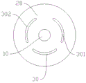
In the figure, 10, screw hole, 20, screw hole pad, 30, arc hole, 301, first edge, 302, second edge.
Detailed Description
The invention is further described with reference to the following figures and embodiments:
the utility model provides an optimize PCB structure of screw hole pad structure, is including locating screw hole pad 20 on the circuit board, sets up screw hole 10 in the screw hole pad 20, evenly sets up arc hole 30 on the screw hole pad 20, and the edge that arc hole 30 is close to screw hole 10 is first edge 301, and the edge that arc hole 30 is close to screw hole pad 20 is second edge 302, and the distance at first edge 301 to screw hole 10 edge equals with the distance at second edge 302 to screw hole pad 20 edge. The width of the arc-shaped hole 30 is 30 to 50 percent of the diameter of the screw hole 10. The area of the screw hole pad 20 is at least 2 times the area of the screw hole 10.
The first embodiment:
as shown in fig. 1, the screw hole bonding pad 20 is rectangular, the inclined upper side of the screw hole bonding pad 20 is provided with the screw hole 10, the area of the screw hole bonding pad 20 is far larger than that of the screw hole 10, the arc hole 30 is arranged at the blank of the screw hole bonding pad 20, specifically, the arc hole 30 is uniformly arranged at the center between the edge of the screw hole 10 and the edge of the screw hole bonding pad 20, so that the distance from the first edge 301 to the edge of the screw hole 10 is the same as the distance from the second edge 302 to the edge of the screw hole bonding pad 20.
Limited by the positions of the screw holes 10 and the space of the pad, in this embodiment, the number of the arc-shaped holes 30 is 2, and the arc-shaped holes 30 are uniformly formed in the blank area of the screw hole pad 20 to enhance the heat dissipation capability.
Preferably, the arcuate aperture 30 is generally short oval in shape.
Preferably, the width of the arc-shaped hole 30 is 50% of the diameter of the screw hole 10. The solder paste brushed on the screw hole bonding pad is prevented from leaking while the structural strength of the heat dissipation bonding pad is increased.
Second embodiment:
as shown in fig. 2, the screw hole pad 20 is circular, the screw hole 10 is formed in the center of the screw hole pad 20, the area of the screw hole pad 20 is much larger than that of the screw hole 10, and the arc-shaped holes 30 are uniformly formed in the blank of the screw hole pad 20, so that the distance from the first edge 301 to the edge of the screw hole 10 is the same as the distance from the second edge 302 to the edge of the screw hole pad 20.
Limited by the positions of the screw holes 10 and the space of the bonding pad, in this embodiment, the number of the arc-shaped holes 30 is 3, and the arc-shaped holes 30 are additionally arranged to fully utilize the redundant space of the screw hole bonding pad 20 to enhance the heat dissipation capability.
Preferably, the arcuate aperture 30 is generally oblong in shape.
Preferably, the diameter of the arc-shaped hole 30 is 30% of the width of the screw hole 10. The solder paste brushed on the screw hole bonding pad is prevented from leaking while the structural strength of the heat dissipation bonding pad is increased.
It will be understood that modifications and variations can be made by persons skilled in the art in light of the above teachings and all such modifications and variations are considered to be within the scope of the invention as defined by the following claims.
The above exemplary description of the present invention is made in conjunction with the accompanying drawings, and it is obvious that the present invention is not limited by the above manner, and various improvements made by the method concept and technical solution of the present invention or by directly applying the concept and technical solution of the present invention to other occasions without improvement are all within the protection scope of the present invention.
Claims (8)
1. A PCB structure for optimizing a screw hole bonding pad structure is characterized by comprising a screw hole bonding pad arranged on a circuit board, wherein screw holes are formed in the screw hole bonding pad, arc-shaped holes are uniformly formed in the screw hole bonding pad,
the arc hole is close to the edge of screw hole is first edge, the arc hole is close to the edge of screw hole pad is the second edge, first edge extremely the distance at screw hole edge with the second edge extremely the distance at screw hole pad edge equals.
2. The PCB structure of an optimized screw hole pad structure of claim 1, wherein the screw hole pad area is at least 2 times the screw hole area.
3. The PCB structure of an optimized screw hole pad structure of claim 1, wherein the width of the arc-shaped hole is 30% to 50% of the diameter of the screw hole.
4. The PCB structure of an optimized screw hole pad structure of claim 1, wherein the number of the arc-shaped holes is at least 2.
5. The PCB structure of an optimized screw hole pad structure of claim 4, wherein the number of the arc-shaped holes is 2.
6. The PCB structure of an optimized screw hole bonding pad structure of claim 5, wherein an angle between the center of the screw hole and the center of the two arc-shaped holes is 90 °.
7. The PCB structure of an optimized screw hole pad structure of claim 4, wherein the number of the arc-shaped holes is 3.
8. The PCB structure of an optimized screw hole bonding pad structure of claim 7, wherein the angle between the center of the screw hole and the center of the adjacent arc-shaped holes is 120 °.
Priority Applications (1)
| Application Number | Priority Date | Filing Date | Title |
|---|---|---|---|
| CN202020507997.0U CN211959654U (en) | 2020-04-09 | 2020-04-09 | PCB structure for optimizing screw hole bonding pad structure |
Applications Claiming Priority (1)
| Application Number | Priority Date | Filing Date | Title |
|---|---|---|---|
| CN202020507997.0U CN211959654U (en) | 2020-04-09 | 2020-04-09 | PCB structure for optimizing screw hole bonding pad structure |
Publications (1)
| Publication Number | Publication Date |
|---|---|
| CN211959654U true CN211959654U (en) | 2020-11-17 |
Family
ID=73161046
Family Applications (1)
| Application Number | Title | Priority Date | Filing Date |
|---|---|---|---|
| CN202020507997.0U Active CN211959654U (en) | 2020-04-09 | 2020-04-09 | PCB structure for optimizing screw hole bonding pad structure |
Country Status (1)
| Country | Link |
|---|---|
| CN (1) | CN211959654U (en) |
-
2020
- 2020-04-09 CN CN202020507997.0U patent/CN211959654U/en active Active
Similar Documents
| Publication | Publication Date | Title |
|---|---|---|
| US6433441B1 (en) | Area array type semiconductor device | |
| US8491337B2 (en) | Electrical connector with shielded recessed portions | |
| US9065216B2 (en) | Electrical connector having a plurality of absorbing material blocks | |
| US6181551B1 (en) | Pin soldering enhancement and method | |
| CN109616452B (en) | Heat radiation assembly, corresponding heat radiation device and corresponding circuit board | |
| CN102843861B (en) | Printed circuit board and printed circuit board combination structure | |
| CN211959654U (en) | PCB structure for optimizing screw hole bonding pad structure | |
| CN109588023B (en) | Heat dissipation structure and related equipment | |
| CN201426229Y (en) | Heat dissipation and electromagnetic interference prevention module | |
| CN112399772B (en) | Heat dissipation and noise shielding combined structure of electronic device | |
| CN109687204B (en) | Electrical connector | |
| TWM586888U (en) | Electrical connector | |
| CN201066957Y (en) | A printed circuit board and meter mounting welding tray | |
| CN215933570U (en) | Heat dissipation cover plate and chip | |
| CN201629939U (en) | Solid-state hard disk | |
| CN108990312A (en) | It is a kind of for welding the steel mesh of QFN | |
| US9356368B2 (en) | Low profile electrical connector | |
| CN113629028A (en) | Heat dissipation cover plate and chip | |
| CN212034442U (en) | Radiating fin grounding structure | |
| CN108615716B (en) | Wireless communication module and wireless communication device comprising same | |
| CN221829151U (en) | A via hole welding disk for BGA encapsulation | |
| CN105578706A (en) | circuit board assembly | |
| JP2001223452A (en) | Circuit board | |
| CN104363698A (en) | Circuit board, row pin package structure thereof and package design method | |
| CN218274569U (en) | W-band millimeter wave chip multilayer dielectric substrate |
Legal Events
| Date | Code | Title | Description |
|---|---|---|---|
| GR01 | Patent grant | ||
| GR01 | Patent grant |