CN210668340U - Heat radiation structure of base plate - Google Patents
Heat radiation structure of base plate Download PDFInfo
- Publication number
- CN210668340U CN210668340U CN201922130681.4U CN201922130681U CN210668340U CN 210668340 U CN210668340 U CN 210668340U CN 201922130681 U CN201922130681 U CN 201922130681U CN 210668340 U CN210668340 U CN 210668340U
- Authority
- CN
- China
- Prior art keywords
- heat dissipation
- chip
- substrate
- dissipation cover
- heat
- Prior art date
- Legal status (The legal status is an assumption and is not a legal conclusion. Google has not performed a legal analysis and makes no representation as to the accuracy of the status listed.)
- Active
Links
Images


Landscapes
- Cooling Or The Like Of Semiconductors Or Solid State Devices (AREA)
Abstract
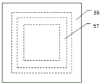
The utility model discloses a heat radiation structure of base plate belongs to semiconductor chip packaging technology field. The heat dissipation cover comprises a heat dissipation cover (55) and heat dissipation cover convex blocks (57), wherein the inner side of a crown of the heat dissipation cover (55) is used for accommodating a chip (60) and the heat dissipation cover convex blocks (57), a brim is fixedly connected with a substrate (10) through bonding glue I (56), the center of the crown is a chip packaging area, the heat dissipation cover convex blocks (57) are arranged around the chip (60) and are insulated from the chip (60), the lower surface of the heat dissipation cover convex blocks (57) is flush with the lower surface of the brim of the heat dissipation cover (55) and is fixedly connected with the substrate (10) through bonding glue II (58), the chip (60) is inversely installed on the substrate (10), the heat dissipation cover (50) is buckled on the substrate (10), and is connected with the back of the chip (60) through a heat dissipation agent (54) and dissipates heat. The utility model discloses reduced the warpage of base plate, improved the bad problem of solder ball coplanarity that heat dissipation glue layering and base plate warpage caused.
Description
Technical Field
The utility model relates to a heat radiation structure of base plate belongs to semiconductor chip packaging technology field.
Background
In the chip package structure, a chip 60 is flip-chip mounted on a substrate 10 (under-fill 62) via an underlying metal or solder ball 61, and the heat dissipation cap 50 is used to assist the heat dissipation of the chip 60, as shown in fig. 1, the heat dissipation cap 50 is generally in the shape of a cap, the inner side of which is bonded to the back surface of the chip 60 via a heat dissipation adhesive 51, and the periphery of which is bonded to the upper surface of the substrate 10 via an adhesive 52. As the chip 60 is larger, the warpage of the substrate, the heat dissipation cover 50 and the chip 60 is not uniform during the heating process due to the different materials of the substrate, the heat dissipation cover and the chip, which often causes the heat dissipation adhesive 51 to have undesirable phenomena such as delamination. In addition, warpage causes poor coplanarity of solder balls on the substrate surface.
Disclosure of Invention
An object of the utility model is to overcome the not enough of existence among the prior art, provide a heat radiation structure of base plate, solve the heat dissipation and glue the poor problem of coplanarity of layering and base plate face solder ball.
The purpose of the utility model is realized like this:
the utility model relates to a heat radiation structure of base plate, it includes heat dissipation lid and heat dissipation lid lug, the heat dissipation lid is the cap form usually, including crown and brim of a hat, the inboard of crown is used for holding chip and a plurality of heat dissipation lid lug, the brim of a hat links firmly with the base plate through bonding glue I, the central authorities of crown of a hat are chip packaging area territory, the heat dissipation lid lug sets up around the chip to it is insulating with the chip, and the lower surface of heat dissipation lid lug flushes with the lower surface of the brim of a hat of heat dissipation lid to glue II through bonding and link firmly with the base plate, the chip is installed on the base plate through the metal or the solder ball below it, and the heat dissipation lid is detained on the base plate, through the back connection and the heat dissipation of coolant and chip.
Optionally, the heat sink cap bump is □ -shaped, surrounding the chip.
Optionally, the heat dissipation cover bump is in a strip shape and arranged in the long side direction of the chip.
Optionally, the heat dissipation cover bumps are symmetrically arranged in the long side direction of the chip.
Optionally, the heat dissipation cover protrusion and the heat dissipation cover are of an integral structure.
Advantageous effects
The utility model relates to a heat radiation structure of base plate sets up the heat dissipation lid lug in the heat dissipation lid inboard, utilizes the heat dissipation lid lug to increase the heat dissipation lid rigidity and increase with the bonding area of base plate to reduce the warpage of base plate, improve the bad problem of solder ball coplanarity that heat dissipation glue layering and base plate warpage caused.
Drawings
FIG. 1 is a cross-sectional view of a conventional substrate after packaging;
fig. 2 is a cross-sectional view of an embodiment of a heat dissipation structure of a substrate according to the present invention;
FIG. 3 is a side view of FIG. 2;
FIG. 4 is a side view of FIG. 2;
in the figure:
Adhesive I56
Heat sink cover bump 57
Adhesive II 58
A chip 60.
Detailed Description
The following describes in detail embodiments of the present invention with reference to the accompanying drawings. Spatially relative terms (such as "below …", "below", "lower", "above …", "upper", and the like) may be used for ease of illustration to describe one element or component's relationship to another element or component as illustrated in the figures. Spatially relative terms may also encompass different orientations of the device in use or operation in addition to the orientation depicted in the figures. The device may be otherwise oriented (rotated 90 degrees or at other orientations) and the spatially relative descriptors used herein interpreted accordingly.
Examples
The utility model relates to a heat radiation structure of base plate, it includes cooling cap 55 and cooling cap lug 57. The chip 60 is flip-chip mounted on the substrate 10 via the metal or solder balls 61 thereunder, and the heat sink 55 is attached to the substrate 10 and is connected to the backside of the chip 60 via the heat spreader 54 for heat dissipation, as shown in fig. 2.
The heat-dissipating cap 55 is generally in the shape of a cap, and includes a crown and a brim, the inner side of the crown is used for accommodating the chip 60 and the plurality of heat-dissipating cap protrusions 57, and the brim is fixedly connected with the substrate 10 through an adhesive I56. Generally, the center of the crown is the chip package area, and the heat-dissipating cap bump 57 is disposed around the chip 60 and insulated from the chip 60. The heat slug 57 is in the shape of □ and surrounds the chip 60 as shown in fig. 3. The heat-radiating cover projection 57 may be a plurality of pieces. The heat-dissipating cap bumps 57 may be in the form of a strip, and a plurality of the heat-dissipating cap bumps are symmetrically arranged in the longitudinal direction of the chip 60, as shown in fig. 4, only one heat-dissipating cap bump 5 is shown in the longitudinal direction of the chip 60. The lower surface of the heat dissipation cover projection 57 is flush with the lower surface of the brim of the heat dissipation cover 55 and is fixedly connected with the substrate 10 through the bonding glue II 58, the rigidity of the heat dissipation cover 55 is increased by utilizing the heat dissipation cover projection 57, the bonding area with the substrate 10 is increased, the warping of the substrate 10 is reduced, and the problem of poor coplanarity of the solder balls caused by heat dissipation glue layering and substrate warping is solved. In particular, the heat sink protrusion 57 and the heat sink 55 are integrally formed.
The above-mentioned embodiments further describe the objects, technical solutions and advantages of the present invention in detail, it should be understood that the above-mentioned embodiments are only specific embodiments of the present invention, and are not intended to limit the protection scope of the present invention. Any modification, equivalent replacement, or improvement made within the spirit and principle of the present invention should be included in the protection scope of the present invention.
Claims (5)
1. A heat dissipation structure of a substrate is characterized by comprising a heat dissipation cover (55) and heat dissipation cover bumps (57), the heat dissipation cover (55) is in a cap shape and comprises a crown and a brim, the inner side of the crown is used for accommodating a chip (60) and a plurality of heat dissipation cover convex blocks (57), the brim is fixedly connected with the substrate (10) through bonding glue I (56), the center of the crown is a chip packaging area, the heat dissipation cover convex block (57) is arranged around the chip (60), and is insulated from the chip (60), the lower surface of the heat-radiating cover bump (57) is flush with the lower surface of the brim of the heat-radiating cover (55), and is fixedly connected with the substrate (10) through an adhesive II (58), the chip (60) is inversely installed on the substrate (10) through a metal or a solder ball (61) below the chip, the heat dissipation cover (55) is buckled on the substrate (10), and is connected with the back surface of the chip (60) through a heat dissipation agent (54) and dissipates heat.
2. The heat dissipation structure of claim 1, wherein the heat sink cap bumps (57) are □ -shaped, surrounding the chip (60).
3. The heat dissipation structure of claim 1, wherein the heat dissipation cap bump (57) has a bar shape and is disposed in a long side direction of the chip (60).
4. The heat dissipation structure of claim 3, wherein the heat dissipation cap bumps (57) are symmetrically arranged in a long side direction of the chip (60).
5. The heat dissipation structure according to any one of claims 1 to 4, wherein the heat dissipation cover protrusion (57) and the heat dissipation cover (55) are of a unitary structure.
Priority Applications (1)
| Application Number | Priority Date | Filing Date | Title |
|---|---|---|---|
| CN201922130681.4U CN210668340U (en) | 2019-12-03 | 2019-12-03 | Heat radiation structure of base plate |
Applications Claiming Priority (1)
| Application Number | Priority Date | Filing Date | Title |
|---|---|---|---|
| CN201922130681.4U CN210668340U (en) | 2019-12-03 | 2019-12-03 | Heat radiation structure of base plate |
Publications (1)
| Publication Number | Publication Date |
|---|---|
| CN210668340U true CN210668340U (en) | 2020-06-02 |
Family
ID=70822269
Family Applications (1)
| Application Number | Title | Priority Date | Filing Date |
|---|---|---|---|
| CN201922130681.4U Active CN210668340U (en) | 2019-12-03 | 2019-12-03 | Heat radiation structure of base plate |
Country Status (1)
| Country | Link |
|---|---|
| CN (1) | CN210668340U (en) |
Cited By (4)
| Publication number | Priority date | Publication date | Assignee | Title |
|---|---|---|---|---|
| CN113270331A (en) * | 2021-05-12 | 2021-08-17 | 湖南越摩先进半导体有限公司 | Packaging method and packaging structure of semiconductor device |
| CN113380725A (en) * | 2021-04-29 | 2021-09-10 | 苏州通富超威半导体有限公司 | Chip packaging structure and packaging method |
| WO2023272637A1 (en) * | 2021-06-30 | 2023-01-05 | 华为技术有限公司 | Packaging heat dissipating cover, chip packaging structure, and electronic device |
| CN119480817A (en) * | 2025-01-15 | 2025-02-18 | 井芯微电子技术(天津)有限公司 | Package structure |
-
2019
- 2019-12-03 CN CN201922130681.4U patent/CN210668340U/en active Active
Cited By (5)
| Publication number | Priority date | Publication date | Assignee | Title |
|---|---|---|---|---|
| CN113380725A (en) * | 2021-04-29 | 2021-09-10 | 苏州通富超威半导体有限公司 | Chip packaging structure and packaging method |
| CN113270331A (en) * | 2021-05-12 | 2021-08-17 | 湖南越摩先进半导体有限公司 | Packaging method and packaging structure of semiconductor device |
| CN113270331B (en) * | 2021-05-12 | 2023-12-01 | 湖南越摩先进半导体有限公司 | Packaging method and packaging structure of semiconductor device |
| WO2023272637A1 (en) * | 2021-06-30 | 2023-01-05 | 华为技术有限公司 | Packaging heat dissipating cover, chip packaging structure, and electronic device |
| CN119480817A (en) * | 2025-01-15 | 2025-02-18 | 井芯微电子技术(天津)有限公司 | Package structure |
Similar Documents
| Publication | Publication Date | Title |
|---|---|---|
| CN210668340U (en) | Heat radiation structure of base plate | |
| US11764169B2 (en) | Semiconductor device package with warpage control structure | |
| EP3690935B1 (en) | Semiconductor package having improved thermal interface between semiconductor die and heat spreading structure | |
| TWI529878B (en) | Hybrid thermal interface material for ic packages with integrated heat spreader | |
| US6188578B1 (en) | Integrated circuit package with multiple heat dissipation paths | |
| US6507104B2 (en) | Semiconductor package with embedded heat-dissipating device | |
| US20090127700A1 (en) | Thermal conductor lids for area array packaged multi-chip modules and methods to dissipate heat from multi-chip modules | |
| US20060249852A1 (en) | Flip-chip semiconductor device | |
| US11749631B2 (en) | Electronic package including a hybrid thermal interface material and low temperature solder patterns to improve package warpage and reliability | |
| JP2008166440A (en) | Semiconductor device | |
| US20230187383A1 (en) | Semiconductor device and manufacturing method thereof | |
| JP2001110926A (en) | Flip chip package | |
| KR102596757B1 (en) | Semiconductor packages having stiffener | |
| CN209843689U (en) | Chip packaging structure | |
| CN210073822U (en) | Packaging structure of chip | |
| US20060043553A1 (en) | Chip package having a heat spreader and method for packaging the same | |
| CN210224006U (en) | Packaging structure of multi-chip | |
| JP2000232186A (en) | Semiconductor device and manufacturing method thereof | |
| CN217485436U (en) | Chip packaging structure | |
| US7256493B2 (en) | Ball grid array housing having a cooling foil | |
| US11742323B2 (en) | Semiconductor structure and method of forming the same | |
| CN213401202U (en) | Packaging structure of chip | |
| KR101459566B1 (en) | Heatslug, semiconductor package comprising the same heatslug, and method for fabricating the same semiconductor package | |
| JPH11238828A (en) | Semiconductor device of bga type package and its manufacture and packaging equipment | |
| CN116072628B (en) | Heat dissipation cover plate for enhancing chip package reliability, package structure and method |
Legal Events
| Date | Code | Title | Description |
|---|---|---|---|
| GR01 | Patent grant | ||
| GR01 | Patent grant |