CN201827857U - Heat conducting structure of LED light source - Google Patents
Heat conducting structure of LED light source Download PDFInfo
- Publication number
- CN201827857U CN201827857U CN2010205447729U CN201020544772U CN201827857U CN 201827857 U CN201827857 U CN 201827857U CN 2010205447729 U CN2010205447729 U CN 2010205447729U CN 201020544772 U CN201020544772 U CN 201020544772U CN 201827857 U CN201827857 U CN 201827857U
- Authority
- CN
- China
- Prior art keywords
- heat dissipation
- dissipation substrate
- heat
- printed circuit
- electrode pads
- Prior art date
- Legal status (The legal status is an assumption and is not a legal conclusion. Google has not performed a legal analysis and makes no representation as to the accuracy of the status listed.)
- Expired - Fee Related
Links
- 230000017525 heat dissipation Effects 0.000 claims abstract description 108
- 239000000758 substrate Substances 0.000 claims abstract description 80
- 239000000919 ceramic Substances 0.000 claims abstract description 21
- 238000009434 installation Methods 0.000 claims abstract description 5
- 230000000149 penetrating effect Effects 0.000 claims abstract description 5
- RYGMFSIKBFXOCR-UHFFFAOYSA-N Copper Chemical compound [Cu] RYGMFSIKBFXOCR-UHFFFAOYSA-N 0.000 claims description 6
- 229910052751 metal Inorganic materials 0.000 claims description 6
- 239000002184 metal Substances 0.000 claims description 6
- 229910010293 ceramic material Inorganic materials 0.000 claims description 5
- 239000004593 Epoxy Substances 0.000 claims description 4
- 239000003822 epoxy resin Substances 0.000 claims description 4
- 239000004744 fabric Substances 0.000 claims description 4
- 239000003365 glass fiber Substances 0.000 claims description 4
- 229920000647 polyepoxide Polymers 0.000 claims description 4
- 229920000642 polymer Polymers 0.000 claims description 4
- 229910001020 Au alloy Inorganic materials 0.000 claims description 2
- 229910001128 Sn alloy Inorganic materials 0.000 claims description 2
- PNEYBMLMFCGWSK-UHFFFAOYSA-N aluminium oxide Inorganic materials [O-2].[O-2].[O-2].[Al+3].[Al+3] PNEYBMLMFCGWSK-UHFFFAOYSA-N 0.000 claims description 2
- PMHQVHHXPFUNSP-UHFFFAOYSA-M copper(1+);methylsulfanylmethane;bromide Chemical compound Br[Cu].CSC PMHQVHHXPFUNSP-UHFFFAOYSA-M 0.000 claims description 2
- 239000003353 gold alloy Substances 0.000 claims description 2
- GPYPVKIFOKLUGD-UHFFFAOYSA-N gold indium Chemical compound [In].[Au] GPYPVKIFOKLUGD-UHFFFAOYSA-N 0.000 claims description 2
- JVPLOXQKFGYFMN-UHFFFAOYSA-N gold tin Chemical compound [Sn].[Au] JVPLOXQKFGYFMN-UHFFFAOYSA-N 0.000 claims description 2
- 230000001788 irregular Effects 0.000 claims description 2
- 238000012545 processing Methods 0.000 abstract description 3
- 238000012546 transfer Methods 0.000 abstract description 2
- 238000010292 electrical insulation Methods 0.000 abstract 1
- 229910052802 copper Inorganic materials 0.000 description 5
- 239000010949 copper Substances 0.000 description 5
- 238000013461 design Methods 0.000 description 5
- 239000000463 material Substances 0.000 description 5
- 230000000694 effects Effects 0.000 description 4
- 239000002131 composite material Substances 0.000 description 3
- 238000009413 insulation Methods 0.000 description 3
- 230000008646 thermal stress Effects 0.000 description 3
- KDLHZDBZIXYQEI-UHFFFAOYSA-N Palladium Chemical compound [Pd] KDLHZDBZIXYQEI-UHFFFAOYSA-N 0.000 description 2
- BQCADISMDOOEFD-UHFFFAOYSA-N Silver Chemical compound [Ag] BQCADISMDOOEFD-UHFFFAOYSA-N 0.000 description 2
- 229910052782 aluminium Inorganic materials 0.000 description 2
- XAGFODPZIPBFFR-UHFFFAOYSA-N aluminium Chemical compound [Al] XAGFODPZIPBFFR-UHFFFAOYSA-N 0.000 description 2
- 230000009286 beneficial effect Effects 0.000 description 2
- 230000005611 electricity Effects 0.000 description 2
- 150000002739 metals Chemical class 0.000 description 2
- 238000000034 method Methods 0.000 description 2
- 229910052709 silver Inorganic materials 0.000 description 2
- 239000004332 silver Substances 0.000 description 2
- 238000005476 soldering Methods 0.000 description 2
- 230000003068 static effect Effects 0.000 description 2
- 229910000838 Al alloy Inorganic materials 0.000 description 1
- 229910000881 Cu alloy Inorganic materials 0.000 description 1
- 238000009825 accumulation Methods 0.000 description 1
- 238000005520 cutting process Methods 0.000 description 1
- 230000007423 decrease Effects 0.000 description 1
- 230000007812 deficiency Effects 0.000 description 1
- 238000011161 development Methods 0.000 description 1
- 238000010586 diagram Methods 0.000 description 1
- 238000005553 drilling Methods 0.000 description 1
- 238000005516 engineering process Methods 0.000 description 1
- 238000005530 etching Methods 0.000 description 1
- 239000003292 glue Substances 0.000 description 1
- PCHJSUWPFVWCPO-UHFFFAOYSA-N gold Chemical compound [Au] PCHJSUWPFVWCPO-UHFFFAOYSA-N 0.000 description 1
- 229910052737 gold Inorganic materials 0.000 description 1
- 239000010931 gold Substances 0.000 description 1
- 239000007770 graphite material Substances 0.000 description 1
- 230000007774 longterm Effects 0.000 description 1
- 238000004519 manufacturing process Methods 0.000 description 1
- 238000004806 packaging method and process Methods 0.000 description 1
- 238000012536 packaging technology Methods 0.000 description 1
- 229910052763 palladium Inorganic materials 0.000 description 1
- 239000002861 polymer material Substances 0.000 description 1
- 230000001681 protective effect Effects 0.000 description 1
- 238000004080 punching Methods 0.000 description 1
- 238000011160 research Methods 0.000 description 1
- 230000035939 shock Effects 0.000 description 1
- 229910000679 solder Inorganic materials 0.000 description 1
- 230000035882 stress Effects 0.000 description 1
- 239000011345 viscous material Substances 0.000 description 1
Images


Landscapes
- Led Device Packages (AREA)
Abstract
本实用新型揭示了一种LED光源的导热结构,是指一散热基板,其单侧或双侧表面设有印刷电路板及其电极焊盘,以及与电极焊盘相连的发光元件,各电极焊盘之间分布有导电线路,其特点是该散热基板顶面或两面为具有尺寸稳定性和散热性的陶瓷层,且于其上对应发光元件的热沉装设位置形成有凹槽;散热基板还设有一个以上自上而下穿透至散热基板底面的散热通孔,围绕凹槽且与印刷电路板的导电线路和电极焊盘不相干涉而设,并在散热基板内设有连通各散热通孔的散热通道。应用本实用新型的技术方案,能有效提高印刷电路板的导热性能、电气绝缘性能和机械加工性能,增强LED产品耐高低温度冲击性能,提高产品的可靠性、稳定性,广泛应用于电子器件的热传递介质。
The utility model discloses a heat-conducting structure of an LED light source, which refers to a heat-dissipating substrate, on which a printed circuit board and its electrode pads are arranged on one or both sides of the surface, and a light-emitting element connected with the electrode pads. There are conductive lines distributed between the plates, which are characterized in that the top or both sides of the heat dissipation substrate are ceramic layers with dimensional stability and heat dissipation, and grooves are formed on it corresponding to the installation position of the heat sink of the light-emitting element; the heat dissipation substrate There is also more than one heat dissipation through hole penetrating from top to bottom to the bottom surface of the heat dissipation substrate, which is arranged around the groove and does not interfere with the conductive lines and electrode pads of the printed circuit board. Thermal vias for thermal channels. Applying the technical scheme of the utility model can effectively improve the thermal conductivity, electrical insulation performance and mechanical processing performance of the printed circuit board, enhance the high and low temperature impact resistance performance of LED products, improve the reliability and stability of the product, and be widely used in electronic devices. heat transfer medium.
Description
技术领域technical field
本实用新型涉及LED照明灯具的散热结构,尤其涉及一种LED光源封装用陶瓷散热结构,属于LED应用技术领域。The utility model relates to a heat dissipation structure of an LED lighting lamp, in particular to a ceramic heat dissipation structure for LED light source packaging, which belongs to the technical field of LED applications.
背景技术Background technique
LED照明光源在许多灯具及相关产品中已逐步开始大量使用,其具有使用寿命长、发光效率高及耗电量等特点,具有取代传统照明光源的趋势。LED lighting sources have gradually begun to be widely used in many lamps and related products. They have the characteristics of long service life, high luminous efficiency and power consumption, and have the tendency to replace traditional lighting sources.
但目前在封装技术的发展中,功率提高及体积越来越小使得中心发热密度越来越高,封装设计仍以多层次封装为基础,造成散热路径上产生大量的热阻,而累积于印刷电路板上热阻最大;同时,散热基板所使用的散热片几乎都是铝合金或铜合金等金属,随着功率及面积的不断增大,导热性能也会达到饱和值,当然发光二极体的温度也就无法有效降低,长时间高温造成LED光衰加剧、寿命缩短,增加了LED失效的可能性。另外,当前技术路线将LED光源芯片与散热基板贴装与一个平面且进行电气连接。这样,散热基板同时具有散热与电气连接作用,如果散热基板在高温下产生热应力及变形,势必会造成电路短路或断路故障,使得整个光源产品失效,因此,散热基板的选择、结构设计尤为重要。However, in the current development of packaging technology, the increase in power and the smaller and smaller volume make the center heat density higher and higher. The thermal resistance on the circuit board is the largest; at the same time, the heat sinks used in the heat dissipation substrate are almost all metals such as aluminum alloy or copper alloy. With the continuous increase of power and area, the thermal conductivity will also reach the saturation value. The temperature of the LED cannot be effectively reduced, and the long-term high temperature will cause the LED light decay to increase and the life to be shortened, increasing the possibility of LED failure. In addition, the current technical route mounts the LED light source chip and the heat dissipation substrate on a plane and electrically connects them. In this way, the heat dissipation substrate has the function of heat dissipation and electrical connection at the same time. If the heat dissipation substrate produces thermal stress and deformation at high temperature, it will inevitably cause a circuit short circuit or open circuit failure, making the entire light source product invalid. Therefore, the selection and structural design of the heat dissipation substrate are particularly important. .
上述的现象表明,一些LED产品只靠封装设计已无法满足高功率LED设计需要,必须由多方位的组合设计来加强散热功能,减小散热效果不佳的问题影响,提高发光二极体的发光效率及使用寿命。因此,如何选择印刷电路板材料绝缘及散热研究已成为目前基板设计的一个重要方向。The above phenomenon shows that some LED products can no longer meet the design needs of high-power LEDs only by package design, and must use multi-directional combination design to strengthen the heat dissipation function, reduce the impact of poor heat dissipation, and improve the light emission of light-emitting diodes. efficiency and service life. Therefore, how to choose printed circuit board material insulation and heat dissipation research has become an important direction of substrate design.
发明内容Contents of the invention
为克服上述现有技术的不足,本实用新型的目的在于将发光二极管封装在散热基板复合结构上,提供一种LED光源的导热结构,利用合理布局的散热通孔和高热传导性的散热基板,避免热能蓄积于印刷电路板中,从而提高LED光源的散热性和绝缘安全性,并可延长发光元件的使用寿命。In order to overcome the deficiencies of the above-mentioned prior art, the purpose of this utility model is to package the light-emitting diodes on the composite structure of the heat dissipation substrate, provide a heat conduction structure of the LED light source, and utilize the heat dissipation through holes with a reasonable layout and the heat dissipation substrate with high thermal conductivity. Avoid heat energy from accumulating in the printed circuit board, thereby improving the heat dissipation and insulation safety of the LED light source, and prolonging the service life of the light-emitting element.
本实用新型的目的,将通过以下技术方案得以实现:The purpose of this utility model will be achieved through the following technical solutions:
LED光源的导热结构,是指一散热基板,所述散热基板上表面设有一印刷电路板及其两个以上的电极焊盘,以及与电极焊盘相连、一个以上的发光元件,所述印刷电路板各电极焊盘之间分布有导电线路,其特征在于:所述散热基板顶面为具有尺寸稳定性和散热性的陶瓷层,且所述陶瓷层对应发光元件的热沉装设位置形成有凹槽;所述散热基板设有一个以上自上而下穿透至散热基板底面的散热通孔,所述散热通孔围绕凹槽而设,与印刷电路板的导电线路和电极焊盘不相干涉,且在所述散热基板内设有连通各散热通孔的散热通道。The heat conduction structure of the LED light source refers to a heat dissipation substrate, the upper surface of the heat dissipation substrate is provided with a printed circuit board and more than two electrode pads, and more than one light-emitting element connected to the electrode pads, the printed circuit board There are conductive lines distributed between the electrode pads of the board, and it is characterized in that: the top surface of the heat dissipation substrate is a ceramic layer with dimensional stability and heat dissipation, and the ceramic layer corresponds to the installation position of the heat sink of the light-emitting element. groove; the heat dissipation substrate is provided with more than one heat dissipation through hole penetrating from top to bottom to the bottom surface of the heat dissipation substrate. interference, and a heat dissipation channel communicating with each heat dissipation through hole is provided in the heat dissipation substrate.
进一步地,前述的LED光源的导热结构,其中该散热基板为氧化铝、氮化铝或完全陶瓷材质的平面板材,或为规则形状、非规则形状的柱体结构。Furthermore, in the heat conduction structure of the aforementioned LED light source, the heat dissipation substrate is a planar plate made of alumina, aluminum nitride or a complete ceramic material, or a regular-shaped or irregular-shaped columnar structure.
进一步地,前述的LED光源的导热结构,其中该印刷电路板的导电线路为铺设在散热基板上的金属铜线,且其电极焊盘的局部设有铟金合金或金锡合金。Furthermore, in the heat conduction structure of the aforementioned LED light source, the conductive lines of the printed circuit board are metal copper wires laid on the heat dissipation substrate, and the electrode pads thereof are partially provided with indium-gold alloy or gold-tin alloy.
进一步地,前述的LED光源的导热结构,其中该印刷电路板的绝缘介质为环氧玻纤布粘结片或环氧树脂聚合物之一。Furthermore, in the heat conduction structure of the aforementioned LED light source, the insulating medium of the printed circuit board is one of epoxy glass fiber cloth bonding sheet or epoxy resin polymer.
进一步地,前述的LED光源的导热结构,其中该散热基板上所设发光元件数量上为一个以上,各发光元件间的导电线路及其电极焊盘为串联结构或并联结构。Furthermore, in the aforementioned thermal conduction structure of the LED light source, the number of light emitting elements provided on the heat dissipation substrate is more than one, and the conductive lines and electrode pads between the light emitting elements are in a series or parallel structure.
本实用新型的目的,还可以通过以下技术方案得以实现:The purpose of this utility model can also be achieved through the following technical solutions:
LED光源的导热结构,是指一散热基板,所述散热基板上、下两侧表面均设有一印刷电路板及其各自两个以上的电极焊盘,以及与电极焊盘相连、两个以上的发光元件,所述各印刷电路板的电极焊盘之间分布有导电线路,其特征在于:所述散热基板为具有尺寸稳定性和散热性的陶瓷结构或顶面及底面均为陶瓷的夹层结构,且所述散热基板的两侧表面对应发光元件的热沉装设位置形成有凹槽,所述凹槽相对散热基板的两侧表面错位;所述散热基板设有一个以上自上而下穿透至散热基板底面的散热通孔,所述散热通孔围绕每一凹槽而设,与印刷电路板的导电线路和电极焊盘不相干涉,且在所述散热基板内设有连通各散热通孔的散热通道。The heat conduction structure of the LED light source refers to a heat dissipation substrate. A printed circuit board and more than two electrode pads are provided on the upper and lower surfaces of the heat dissipation substrate, and more than two electrode pads are connected to the electrode pads. The light-emitting element has conductive lines distributed between the electrode pads of the printed circuit boards, and is characterized in that the heat dissipation substrate is a ceramic structure with dimensional stability and heat dissipation or a sandwich structure with ceramic top and bottom surfaces , and grooves are formed on both sides of the heat dissipation substrate corresponding to the installation position of the heat sink of the light-emitting element, and the grooves are misaligned relative to the two sides of the heat dissipation substrate; The heat dissipation through holes penetrating to the bottom surface of the heat dissipation substrate, the heat dissipation through holes are arranged around each groove, and do not interfere with the conductive lines and electrode pads of the printed circuit board, and are provided in the heat dissipation substrate to communicate with each heat dissipation Through-hole thermal channels.
进一步地,前述的LED光源的导热结构,其中该散热基板两侧的印刷电路板相对独立或相互导联。Further, in the aforementioned heat conduction structure of the LED light source, the printed circuit boards on both sides of the heat dissipation substrate are relatively independent or connected to each other.
实施本实用新型的技术方案,其有益效果体现在:Implement the technical scheme of the utility model, its beneficial effect is reflected in:
(1)选用陶瓷散热基板热传导率超过铝材料,具有比铝材料更好的导热性,且重量也比铜轻,以保持散热器的轻便,提高了LED封装基板的散热性能,改善因温升导致LED芯片光衰大及寿命下降的问题;(1) The thermal conductivity of ceramic heat dissipation substrate is higher than that of aluminum material, which has better thermal conductivity than aluminum material, and its weight is lighter than copper, so as to keep the radiator light, improve the heat dissipation performance of LED package substrate, and improve the temperature rise caused by Lead to the problem of large light decay and lifespan decline of LED chips;
(2)LED散热基板结构的热膨胀率小,具有优异的散热性能,其散热效果卓越;陶瓷材料热膨胀系数与LED芯片接近,受热基材膨胀变化差异小,避免铜线路和金属化孔间断裂而造成破坏;(2) The thermal expansion rate of the LED heat dissipation substrate structure is small, and it has excellent heat dissipation performance, and its heat dissipation effect is excellent; the thermal expansion coefficient of the ceramic material is close to that of the LED chip, and the difference in the expansion change of the heated substrate is small, avoiding the fracture between the copper line and the metallized hole. cause damage;
(3)抗热应力性强:陶瓷散热基板在常温下使用时能经受住温度的剧变而不致破坏,耐高低温度冲击性能强,提高LED产品的可靠性、稳定性;(3) Strong thermal stress resistance: The ceramic heat dissipation substrate can withstand drastic changes in temperature without damage when used at room temperature, and has strong resistance to high and low temperature shocks, improving the reliability and stability of LED products;
(4)陶瓷散热基板具有高机械强度和韧性,在陶瓷散热基板上可实现大面积的印制板的制造,能够有效地克服导电层、基板之间因不同膨胀系数而引起的应力效应,可承受钻孔、冲剪、切割、蚀刻等加工;(4) The ceramic heat dissipation substrate has high mechanical strength and toughness, and the manufacture of large-area printed boards can be realized on the ceramic heat dissipation substrate, which can effectively overcome the stress effect caused by different expansion coefficients between the conductive layer and the substrate. Withstand drilling, punching, cutting, etching and other processing;
(5)防静电性能较好,陶瓷或石墨材质本身,能够有效扩散静电,防止静电击穿电器元件。(5) The anti-static performance is good. The ceramic or graphite material itself can effectively diffuse static electricity and prevent static electricity from breaking down electrical components.
附图说明Description of drawings
图1是本实用新型LED光源导热结构一实施例的立体结构俯视示意图;Fig. 1 is a schematic top view of the three-dimensional structure of an embodiment of the heat conduction structure of the LED light source of the present invention;
图2是图1中A-A线的剖面结构示意图;Fig. 2 is the sectional structural representation of line A-A in Fig. 1;
图3是本实用新型LED光源导热结构另一实施例的剖面结构示意图。Fig. 3 is a schematic cross-sectional structure diagram of another embodiment of the heat conduction structure of the LED light source of the present invention.
具体实施方式Detailed ways
为使本实用新型的技术特征及应用后的有益效果更清楚、易于理解,以下结合本实用新型若干选实施例及其附图对本实用新型作进一步地详细说明。然而,除了该详细描述之外,本实用新型还可以广泛地在其他的实施方式实行。亦即,本实用新型的范围不受已提出之实施方式的限制,而应以本实用新型提出之申请专利范围为准。In order to make the technical features of the utility model and the beneficial effects after application clearer and easier to understand, the utility model will be further described in detail below in combination with several selected embodiments of the utility model and accompanying drawings. However, the invention can be broadly practiced in other embodiments than this detailed description. That is to say, the scope of the present utility model is not limited by the proposed embodiments, but should be based on the patent scope of the utility model.
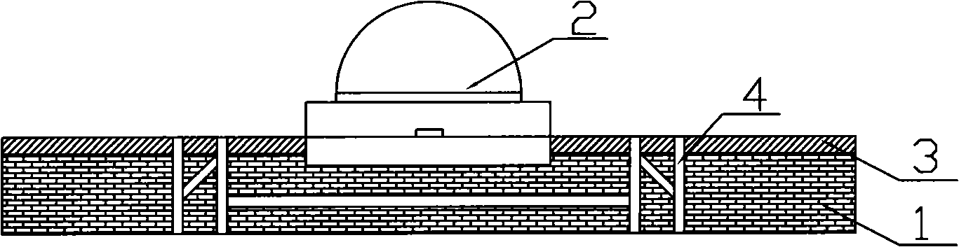
如图1所示,为本实用新型LED光源的导热结构之第一较佳实施例的结构分解图,本LED光源的导热结构主要结构包含有:一个散热基板1,其可以为顶面具有尺寸稳定性及散热性的陶瓷层或完全为陶瓷结构(本实施例优选完全为陶瓷结构),该散热基板1上有一印刷电路板3,印刷电路板3上表面且分布有导电线路及电极焊盘(常规技术未标识),放置光源热沉的区域具有凹槽,发光元件2或发光元件贴合于此散热基板1上的具有凹槽区域内,该印刷电路板3上具有两个或两个以上电极焊盘,并由金属导线将发光元件两端的电极与该印刷电路板3上的电极焊盘相连接,散热基板1用于承受机械及热应力。特别地,该散热基板1具有若干个散热通孔4,所述散热通孔4自上而下透过印刷电路板直达散热基板的底层,散热通孔4包围在发光元件2的热沉四周,并与导电线路或电极焊盘保持一定距离,基板内散热通孔4彼此之间还有散热通道,以防止局部热量积聚。As shown in Figure 1, it is an exploded view of the structure of the first preferred embodiment of the heat conduction structure of the LED light source of the present invention. The main structure of the heat conduction structure of the LED light source includes: a heat dissipation substrate 1, which can be a top surface with a size Stable and heat-dissipating ceramic layer or completely ceramic structure (this embodiment is preferably completely ceramic structure), a printed
该散热基板1为非金属陶瓷材质,其形状为平面板材,也可以是规则形状或非规则形状的柱体结构,如菱形柱体或方形柱体,只要可以与发光元件2热沉座层匹配即可。此外,以较佳实施例中平面板材结构为例,该散热基板1的材质可为高分子材料、陶瓷材料或前述两者所形成的复合材料,该散热基板1的上表面与该印刷电路板3的下表面相对应,并由环氧玻纤布粘结片或者特殊的高导热环氧树脂聚合物等黏性物质黏合方式,让散热基板1与印刷电路板3固定结合成一体,在该印刷电路板3的上板面电极经焊锡焊接方式与光源电极一一对应连接,在散热基板1与印刷电路板3的上下表面及复数个贯穿两个面之散热通孔,而形成发光二极体复合结构散热基板1。The heat dissipation substrate 1 is made of non-metallic ceramic material, and its shape is a flat plate, and it can also be a regular or irregular cylindrical structure, such as a rhombus or a square cylinder, as long as it can match the heat sink layer of the light emitting element 2 That's it. In addition, taking the planar plate structure in the preferred embodiment as an example, the material of the heat dissipation substrate 1 can be a polymer material, a ceramic material, or a composite material formed by the two, and the upper surface of the heat dissipation substrate 1 and the printed circuit board The lower surface of 3 corresponds to the lower surface, and is bonded with viscous substances such as epoxy glass fiber cloth or special high thermal conductivity epoxy resin polymer, so that the heat dissipation substrate 1 and the printed
上述的发光元件2嵌入印刷电路板3的对应凹槽区域内的镂孔内,并与下方的非金属基的散热基板1接触,散热基板1位于LED光源2的热沉正下方,光源热沉与其内表面壁充分接触,热量沿板面均匀传递,环绕四周的散热通孔将热量均匀的对流传到空气中。The above-mentioned light-emitting element 2 is embedded in the hollow hole in the corresponding groove area of the printed
该发光元件2及其电极贴装固定于印刷电路板3的表面电极焊盘上,固定方式可使用锡膏、导电银胶涂敷或是用锡焊的方式固定,光源器件的电极或引脚以并联或串联结构方式排布。The light-emitting element 2 and its electrodes are mounted and fixed on the surface electrode pads of the printed
该印刷电路板3上分布有导电线路以及电极焊盘,其材质选择上一般采用高导热的环氧玻纤布粘结片或者特殊的高导热环氧树脂聚合物,其底层导热层为高导热的陶瓷基板,具有很强的尺寸稳定性和机械加工性能及优良的散热性。发光元件2的热沉与陶瓷基板表面紧密接触,热沉的四周与印刷电路板3的绝缘介质紧密贴合,构成两层结构的基板结构,如图2所示。The printed
上述印刷电路板3贴覆散热基板1后,即可在印刷电路板3外层加工导电层,并布置导电线路,或在绝缘层的外面全部覆盖导电层,再在导电层上面蚀刻制作导电线路;并在绝缘层的外面局部涂覆防护膜,其中,该导电线路采用金属铜来制作,电极焊盘还可以使用或在铜层上辅助使用金、银、钯等金属来制作导电线路。After the above-mentioned printed
除上述单导电层的基板结构外,本实用新型的LED光源的导热结构的还可为双面结构。如图3所示,在散热基板1的相对面也可布置导电线路及发光元件2。散热基板1结构与前述的方案相似,区别在于,在陶瓷散热基板1相对面再黏合一层印刷电路板,发光元件贴装在散热基板两侧相错位的凹槽区域内,上下两面的所形成的具有凹槽区域错位交叉排列,而散热通孔4则分布于两者的缝隙之中,与两侧的导电线路及电极焊盘均不相干涉,以便能够更好地取得散热效果。In addition to the above substrate structure with a single conductive layer, the heat conduction structure of the LED light source of the present invention can also be a double-sided structure. As shown in FIG. 3 , conductive lines and light emitting elements 2 can also be arranged on the opposite surface of the heat dissipation substrate 1 . The structure of the heat dissipation substrate 1 is similar to the above-mentioned scheme, the difference is that a layer of printed circuit board is glued on the opposite surface of the ceramic heat dissipation substrate 1, and the light-emitting elements are mounted in the groove areas on both sides of the heat dissipation substrate that are misaligned. The areas with grooves are dislocated and cross-arranged, and the heat dissipation vias 4 are distributed in the gap between them, and do not interfere with the conductive lines and electrode pads on both sides, so as to achieve better heat dissipation effect.
综上所述,LED散热基板导热结构具有良好的导热性能、绝缘性能和机械加工性能,大幅度提高LED光源的导热效果,提高了产品可靠性和稳定性,延长了产品的使用寿命,广泛应用于电子器件的热传递介质,提高工作效率。In summary, the heat conduction structure of the LED heat dissipation substrate has good thermal conductivity, insulation performance and mechanical processing performance, which greatly improves the heat conduction effect of the LED light source, improves product reliability and stability, prolongs the service life of the product, and is widely used Used as a heat transfer medium for electronic devices to improve work efficiency.
Claims (7)
Priority Applications (1)
| Application Number | Priority Date | Filing Date | Title |
|---|---|---|---|
| CN2010205447729U CN201827857U (en) | 2010-09-28 | 2010-09-28 | Heat conducting structure of LED light source |
Applications Claiming Priority (1)
| Application Number | Priority Date | Filing Date | Title |
|---|---|---|---|
| CN2010205447729U CN201827857U (en) | 2010-09-28 | 2010-09-28 | Heat conducting structure of LED light source |
Publications (1)
| Publication Number | Publication Date |
|---|---|
| CN201827857U true CN201827857U (en) | 2011-05-11 |
Family
ID=43966387
Family Applications (1)
| Application Number | Title | Priority Date | Filing Date |
|---|---|---|---|
| CN2010205447729U Expired - Fee Related CN201827857U (en) | 2010-09-28 | 2010-09-28 | Heat conducting structure of LED light source |
Country Status (1)
| Country | Link |
|---|---|
| CN (1) | CN201827857U (en) |
Cited By (11)
| Publication number | Priority date | Publication date | Assignee | Title |
|---|---|---|---|---|
| CN102593317A (en) * | 2011-12-20 | 2012-07-18 | 西安炬光科技有限公司 | High-power high-brightness light-emitting diode (LED) light source packaging structure and packaging method thereof |
| CN102956787A (en) * | 2011-08-16 | 2013-03-06 | 欧司朗股份有限公司 | Electronic module, light emitting device and manufacture method of electronic module |
| CN103378266A (en) * | 2012-04-24 | 2013-10-30 | 新世纪光电股份有限公司 | Substrate structure |
| WO2014015653A1 (en) * | 2012-07-23 | 2014-01-30 | 贵州光浦森光电有限公司 | Method for forming led bulb with high interchangeability and universality and integrated led bulb and lamp |
| CN105810806A (en) * | 2016-04-22 | 2016-07-27 | 江门市迪司利光电股份有限公司 | LED packaging structure having uniform colour temperature and good heat dissipation |
| CN109424864A (en) * | 2017-08-31 | 2019-03-05 | 京东方科技集团股份有限公司 | Light-source structure, electronic device and light-source structure production method |
| CN109695826A (en) * | 2019-03-01 | 2019-04-30 | 力普士科技(珠海)有限公司 | Integral type UV-LED light source module group and preparation method thereof |
| CN110352632A (en) * | 2017-03-02 | 2019-10-18 | 黑拉有限责任两合公司 | Method for manufacturing electric component |
| CN110557878A (en) * | 2018-05-31 | 2019-12-10 | 南昌欧菲生物识别技术有限公司 | Circuit board assembly, photoelectric module, depth camera and electronic device |
| CN112923322A (en) * | 2017-03-31 | 2021-06-08 | 法雷奥照明公司 | Electric energy supply device |
| CN115460763A (en) * | 2022-09-29 | 2022-12-09 | 深圳市思坦科技有限公司 | A printed circuit board, preparation method and display device |
-
2010
- 2010-09-28 CN CN2010205447729U patent/CN201827857U/en not_active Expired - Fee Related
Cited By (14)
| Publication number | Priority date | Publication date | Assignee | Title |
|---|---|---|---|---|
| CN102956787A (en) * | 2011-08-16 | 2013-03-06 | 欧司朗股份有限公司 | Electronic module, light emitting device and manufacture method of electronic module |
| CN102593317B (en) * | 2011-12-20 | 2014-12-24 | 西安炬光科技有限公司 | High-power high-brightness light-emitting diode (LED) light source packaging structure and packaging method thereof |
| CN102593317A (en) * | 2011-12-20 | 2012-07-18 | 西安炬光科技有限公司 | High-power high-brightness light-emitting diode (LED) light source packaging structure and packaging method thereof |
| CN103378266A (en) * | 2012-04-24 | 2013-10-30 | 新世纪光电股份有限公司 | Substrate structure |
| US9625111B2 (en) | 2012-07-23 | 2017-04-18 | Guizhou Gzgps Co., Ltd. | Method for forming LED bulb with high interchangeability and universality and integrated LED bulb and lamp |
| WO2014015653A1 (en) * | 2012-07-23 | 2014-01-30 | 贵州光浦森光电有限公司 | Method for forming led bulb with high interchangeability and universality and integrated led bulb and lamp |
| CN105810806A (en) * | 2016-04-22 | 2016-07-27 | 江门市迪司利光电股份有限公司 | LED packaging structure having uniform colour temperature and good heat dissipation |
| CN110352632A (en) * | 2017-03-02 | 2019-10-18 | 黑拉有限责任两合公司 | Method for manufacturing electric component |
| CN112923322A (en) * | 2017-03-31 | 2021-06-08 | 法雷奥照明公司 | Electric energy supply device |
| CN112923322B (en) * | 2017-03-31 | 2024-02-09 | 法雷奥照明公司 | Electric energy supply device |
| CN109424864A (en) * | 2017-08-31 | 2019-03-05 | 京东方科技集团股份有限公司 | Light-source structure, electronic device and light-source structure production method |
| CN110557878A (en) * | 2018-05-31 | 2019-12-10 | 南昌欧菲生物识别技术有限公司 | Circuit board assembly, photoelectric module, depth camera and electronic device |
| CN109695826A (en) * | 2019-03-01 | 2019-04-30 | 力普士科技(珠海)有限公司 | Integral type UV-LED light source module group and preparation method thereof |
| CN115460763A (en) * | 2022-09-29 | 2022-12-09 | 深圳市思坦科技有限公司 | A printed circuit board, preparation method and display device |
Similar Documents
| Publication | Publication Date | Title |
|---|---|---|
| CN201827857U (en) | Heat conducting structure of LED light source | |
| CN102907183B (en) | For the plating systems of LED | |
| CN101335319B (en) | High-power LED ceramic package base and productive technology | |
| KR101049698B1 (en) | LED array module and manufacturing method thereof | |
| CN101198216A (en) | Flexible circuit board for LED lighting array | |
| CN101645478A (en) | Light emitting diode (LED) radiating structure | |
| CN102610735B (en) | Light-emitting device with thermoelectric separated structure and manufacturing method of light-emitting device | |
| CN205082059U (en) | heat dissipation circuit board | |
| CN203481273U (en) | LED light source module based on AlSiC composite substrate | |
| WO2011057433A1 (en) | Light emitting diode lamp bar and manufacture method thereof, light emitting diode lamp tube | |
| US20100301359A1 (en) | Light Emitting Diode Package Structure | |
| JP2016539508A (en) | Mounting assembly and light emitting device | |
| US20130313606A1 (en) | Illuminating device | |
| CN201796950U (en) | light emitting diode light source structure | |
| WO2010006475A1 (en) | A ceramic packaging substrate for the high power led | |
| CN201766098U (en) | A zero thermal resistance structure of high-power LED and heat sink and LED lamp | |
| CN103247742B (en) | A kind of LED heat radiation substrate and manufacture method thereof | |
| EP2484969A1 (en) | Led energy-saving lamp | |
| CN202103098U (en) | Heat conduction structure | |
| CN201100917Y (en) | High-efficiency LED packaging structure | |
| CN201225594Y (en) | Improved heat conduction structure of substrate | |
| CN203013789U (en) | Semiconductor chip heat dissipation substrate and semiconductor chip packaging structure | |
| CN116314560A (en) | LED chip packaging structure, light-emitting products | |
| CN201000887Y (en) | Rectifier diode bare crystal structure on radiating fin | |
| CN109524374B (en) | LED light-emitting module |
Legal Events
| Date | Code | Title | Description |
|---|---|---|---|
| C14 | Grant of patent or utility model | ||
| GR01 | Patent grant | ||
| CF01 | Termination of patent right due to non-payment of annual fee |
Granted publication date: 20110511 Termination date: 20180928 |
|
| CF01 | Termination of patent right due to non-payment of annual fee |