CN1989787A - Electroluminescent devices with low work function anode - Google Patents
Electroluminescent devices with low work function anode Download PDFInfo
- Publication number
- CN1989787A CN1989787A CNA2003801000992A CN200380100099A CN1989787A CN 1989787 A CN1989787 A CN 1989787A CN A2003801000992 A CNA2003801000992 A CN A2003801000992A CN 200380100099 A CN200380100099 A CN 200380100099A CN 1989787 A CN1989787 A CN 1989787A
- Authority
- CN
- China
- Prior art keywords
- anode
- layer
- replacement
- oxide
- negative electrode
- Prior art date
- Legal status (The legal status is an assumption and is not a legal conclusion. Google has not performed a legal analysis and makes no representation as to the accuracy of the status listed.)
- Granted
Links
Images


Classifications
-
- H—ELECTRICITY
- H05—ELECTRIC TECHNIQUES NOT OTHERWISE PROVIDED FOR
- H05B—ELECTRIC HEATING; ELECTRIC LIGHT SOURCES NOT OTHERWISE PROVIDED FOR; CIRCUIT ARRANGEMENTS FOR ELECTRIC LIGHT SOURCES, IN GENERAL
- H05B33/00—Electroluminescent light sources
- H05B33/12—Light sources with substantially two-dimensional radiating surfaces
- H05B33/26—Light sources with substantially two-dimensional radiating surfaces characterised by the composition or arrangement of the conductive material used as an electrode
-
- H—ELECTRICITY
- H05—ELECTRIC TECHNIQUES NOT OTHERWISE PROVIDED FOR
- H05B—ELECTRIC HEATING; ELECTRIC LIGHT SOURCES NOT OTHERWISE PROVIDED FOR; CIRCUIT ARRANGEMENTS FOR ELECTRIC LIGHT SOURCES, IN GENERAL
- H05B33/00—Electroluminescent light sources
- H05B33/12—Light sources with substantially two-dimensional radiating surfaces
- H05B33/14—Light sources with substantially two-dimensional radiating surfaces characterised by the chemical or physical composition or the arrangement of the electroluminescent material, or by the simultaneous addition of the electroluminescent material in or onto the light source
-
- C—CHEMISTRY; METALLURGY
- C09—DYES; PAINTS; POLISHES; NATURAL RESINS; ADHESIVES; COMPOSITIONS NOT OTHERWISE PROVIDED FOR; APPLICATIONS OF MATERIALS NOT OTHERWISE PROVIDED FOR
- C09K—MATERIALS FOR MISCELLANEOUS APPLICATIONS, NOT PROVIDED FOR ELSEWHERE
- C09K11/00—Luminescent, e.g. electroluminescent, chemiluminescent materials
- C09K11/06—Luminescent, e.g. electroluminescent, chemiluminescent materials containing organic luminescent materials
-
- H—ELECTRICITY
- H10—SEMICONDUCTOR DEVICES; ELECTRIC SOLID-STATE DEVICES NOT OTHERWISE PROVIDED FOR
- H10K—ORGANIC ELECTRIC SOLID-STATE DEVICES
- H10K50/00—Organic light-emitting devices
- H10K50/10—OLEDs or polymer light-emitting diodes [PLED]
- H10K50/17—Carrier injection layers
-
- H—ELECTRICITY
- H10—SEMICONDUCTOR DEVICES; ELECTRIC SOLID-STATE DEVICES NOT OTHERWISE PROVIDED FOR
- H10K—ORGANIC ELECTRIC SOLID-STATE DEVICES
- H10K50/00—Organic light-emitting devices
- H10K50/80—Constructional details
- H10K50/805—Electrodes
- H10K50/81—Anodes
-
- H—ELECTRICITY
- H10—SEMICONDUCTOR DEVICES; ELECTRIC SOLID-STATE DEVICES NOT OTHERWISE PROVIDED FOR
- H10K—ORGANIC ELECTRIC SOLID-STATE DEVICES
- H10K50/00—Organic light-emitting devices
- H10K50/80—Constructional details
- H10K50/805—Electrodes
- H10K50/81—Anodes
- H10K50/818—Reflective anodes, e.g. ITO combined with thick metallic layers
-
- H—ELECTRICITY
- H10—SEMICONDUCTOR DEVICES; ELECTRIC SOLID-STATE DEVICES NOT OTHERWISE PROVIDED FOR
- H10K—ORGANIC ELECTRIC SOLID-STATE DEVICES
- H10K85/00—Organic materials used in the body or electrodes of devices covered by this subclass
- H10K85/60—Organic compounds having low molecular weight
- H10K85/649—Aromatic compounds comprising a hetero atom
- H10K85/657—Polycyclic condensed heteroaromatic hydrocarbons
- H10K85/6572—Polycyclic condensed heteroaromatic hydrocarbons comprising only nitrogen in the heteroaromatic polycondensed ring system, e.g. phenanthroline or carbazole
-
- C—CHEMISTRY; METALLURGY
- C09—DYES; PAINTS; POLISHES; NATURAL RESINS; ADHESIVES; COMPOSITIONS NOT OTHERWISE PROVIDED FOR; APPLICATIONS OF MATERIALS NOT OTHERWISE PROVIDED FOR
- C09K—MATERIALS FOR MISCELLANEOUS APPLICATIONS, NOT PROVIDED FOR ELSEWHERE
- C09K2211/00—Chemical nature of organic luminescent or tenebrescent compounds
- C09K2211/10—Non-macromolecular compounds
- C09K2211/1018—Heterocyclic compounds
- C09K2211/1025—Heterocyclic compounds characterised by ligands
- C09K2211/1044—Heterocyclic compounds characterised by ligands containing two nitrogen atoms as heteroatoms
-
- H—ELECTRICITY
- H10—SEMICONDUCTOR DEVICES; ELECTRIC SOLID-STATE DEVICES NOT OTHERWISE PROVIDED FOR
- H10K—ORGANIC ELECTRIC SOLID-STATE DEVICES
- H10K2101/00—Properties of the organic materials covered by group H10K85/00
- H10K2101/50—Oxidation-reduction potentials, e.g. excited state redox potentials
-
- H—ELECTRICITY
- H10—SEMICONDUCTOR DEVICES; ELECTRIC SOLID-STATE DEVICES NOT OTHERWISE PROVIDED FOR
- H10K—ORGANIC ELECTRIC SOLID-STATE DEVICES
- H10K2102/00—Constructional details relating to the organic devices covered by this subclass
- H10K2102/301—Details of OLEDs
- H10K2102/302—Details of OLEDs of OLED structures
- H10K2102/3023—Direction of light emission
- H10K2102/3026—Top emission
-
- H—ELECTRICITY
- H10—SEMICONDUCTOR DEVICES; ELECTRIC SOLID-STATE DEVICES NOT OTHERWISE PROVIDED FOR
- H10K—ORGANIC ELECTRIC SOLID-STATE DEVICES
- H10K50/00—Organic light-emitting devices
- H10K50/10—OLEDs or polymer light-emitting diodes [PLED]
- H10K50/14—Carrier transporting layers
-
- H—ELECTRICITY
- H10—SEMICONDUCTOR DEVICES; ELECTRIC SOLID-STATE DEVICES NOT OTHERWISE PROVIDED FOR
- H10K—ORGANIC ELECTRIC SOLID-STATE DEVICES
- H10K50/00—Organic light-emitting devices
- H10K50/80—Constructional details
- H10K50/805—Electrodes
-
- H—ELECTRICITY
- H10—SEMICONDUCTOR DEVICES; ELECTRIC SOLID-STATE DEVICES NOT OTHERWISE PROVIDED FOR
- H10K—ORGANIC ELECTRIC SOLID-STATE DEVICES
- H10K85/00—Organic materials used in the body or electrodes of devices covered by this subclass
- H10K85/30—Coordination compounds
- H10K85/321—Metal complexes comprising a group IIIA element, e.g. Tris (8-hydroxyquinoline) gallium [Gaq3]
- H10K85/324—Metal complexes comprising a group IIIA element, e.g. Tris (8-hydroxyquinoline) gallium [Gaq3] comprising aluminium, e.g. Alq3
-
- H—ELECTRICITY
- H10—SEMICONDUCTOR DEVICES; ELECTRIC SOLID-STATE DEVICES NOT OTHERWISE PROVIDED FOR
- H10K—ORGANIC ELECTRIC SOLID-STATE DEVICES
- H10K85/00—Organic materials used in the body or electrodes of devices covered by this subclass
- H10K85/60—Organic compounds having low molecular weight
- H10K85/615—Polycyclic condensed aromatic hydrocarbons, e.g. anthracene
- H10K85/626—Polycyclic condensed aromatic hydrocarbons, e.g. anthracene containing more than one polycyclic condensed aromatic rings, e.g. bis-anthracene
-
- H—ELECTRICITY
- H10—SEMICONDUCTOR DEVICES; ELECTRIC SOLID-STATE DEVICES NOT OTHERWISE PROVIDED FOR
- H10K—ORGANIC ELECTRIC SOLID-STATE DEVICES
- H10K85/00—Organic materials used in the body or electrodes of devices covered by this subclass
- H10K85/60—Organic compounds having low molecular weight
- H10K85/631—Amine compounds having at least two aryl rest on at least one amine-nitrogen atom, e.g. triphenylamine
-
- H—ELECTRICITY
- H10—SEMICONDUCTOR DEVICES; ELECTRIC SOLID-STATE DEVICES NOT OTHERWISE PROVIDED FOR
- H10K—ORGANIC ELECTRIC SOLID-STATE DEVICES
- H10K85/00—Organic materials used in the body or electrodes of devices covered by this subclass
- H10K85/60—Organic compounds having low molecular weight
- H10K85/649—Aromatic compounds comprising a hetero atom
- H10K85/654—Aromatic compounds comprising a hetero atom comprising only nitrogen as heteroatom
-
- H—ELECTRICITY
- H10—SEMICONDUCTOR DEVICES; ELECTRIC SOLID-STATE DEVICES NOT OTHERWISE PROVIDED FOR
- H10K—ORGANIC ELECTRIC SOLID-STATE DEVICES
- H10K85/00—Organic materials used in the body or electrodes of devices covered by this subclass
- H10K85/731—Liquid crystalline materials
-
- Y—GENERAL TAGGING OF NEW TECHNOLOGICAL DEVELOPMENTS; GENERAL TAGGING OF CROSS-SECTIONAL TECHNOLOGIES SPANNING OVER SEVERAL SECTIONS OF THE IPC; TECHNICAL SUBJECTS COVERED BY FORMER USPC CROSS-REFERENCE ART COLLECTIONS [XRACs] AND DIGESTS
- Y10—TECHNICAL SUBJECTS COVERED BY FORMER USPC
- Y10S—TECHNICAL SUBJECTS COVERED BY FORMER USPC CROSS-REFERENCE ART COLLECTIONS [XRACs] AND DIGESTS
- Y10S428/00—Stock material or miscellaneous articles
- Y10S428/917—Electroluminescent
Landscapes
- Physics & Mathematics (AREA)
- Optics & Photonics (AREA)
- Chemical & Material Sciences (AREA)
- Engineering & Computer Science (AREA)
- Materials Engineering (AREA)
- Organic Chemistry (AREA)
- Spectroscopy & Molecular Physics (AREA)
- Electroluminescent Light Sources (AREA)
- Illuminated Signs And Luminous Advertising (AREA)
- Nitrogen Condensed Heterocyclic Rings (AREA)
Abstract
Description
相关申请related application
本申请要求以2002年12月11日提出的韩国专利申请No.2002-78809为基础的外国优先权,该申请由此在本文全面引入供参考。This application claims foreign priority based on Korean Patent Application No. 2002-78809 filed on December 11, 2002, which is hereby incorporated by reference herein in its entirety.
技术领域technical field
本发明涉及显示技术。更具体地说,本发明涉及有机电致发光器件。The present invention relates to display technology. More specifically, the present invention relates to organic electroluminescent devices.
背景技术Background technique
有机发光或有机电致发光是电流通过有机化合物的内在过程转化为可见光的现象的例子。具有荧光或磷光特性的有机化合物在施加电流时产生了光发射。有机荧光和磷光分子均被称为有机发光化合物。Organic luminescence or organic electroluminescence is an example of a phenomenon in which electrical current is converted into visible light by an intrinsic process in organic compounds. Organic compounds with fluorescent or phosphorescent properties produce light emission when an electric current is applied. Both organic fluorescent and phosphorescent molecules are referred to as organic light-emitting compounds.
有机发光或电致发光器件一般由两个对置的电极和插入在该两个电极之间的至少一层组成。在电极之间的该至少一层含有至少一种有机发光化合物。统被称为载流子的电子和空穴从该两个电极(阴极和阳极)被注入到该层中。在施加适当的电能时,阴极将电子注入到插入层中,而阳极将空穴注入到同一层中。An organic light-emitting or electroluminescent device generally consists of two opposing electrodes and at least one layer interposed between the two electrodes. The at least one layer between the electrodes contains at least one organic light emitting compound. Electrons and holes, collectively called carriers, are injected into the layer from the two electrodes (cathode and anode). When the appropriate electrical energy is applied, the cathode injects electrons into the intercalation layer, while the anode injects holes into the same layer.
在许多因素中,有机电致发光器件的性能取决于从电极注入的载流子的量。所注入的载流子越多,越是有可能具有高的发光或亮度。为了在低驱动电压下从电极注入大量的载流子,电极的材料被选择,从而使得其容易注入载流子。阳极一般由具有高功函数的材料制成。阴极一般由具有低功函数的材料制成。在单一电致发光器件中,阳极材料的功函数高于阴极材料的功函数。The performance of an organic electroluminescent device depends on the amount of carriers injected from the electrodes, among many factors. The more carriers injected, the more likely it is to have high luminescence or brightness. In order to inject a large amount of carriers from the electrode at a low driving voltage, the material of the electrode is selected such that it is easy to inject carriers. The anode is generally made of a material with a high work function. The cathode is generally made of a material with a low work function. In a single electroluminescent device, the work function of the anode material is higher than that of the cathode material.
此外,为了在低驱动电压下从电极注入大量的载流子,可以引入载流子注入层。载流子注入层目的是促进从电极注入载流子。空穴注入层可以在阳极侧形成,与阴极面对。电子注入层可以在阴极侧形成,与阳极面对。载流子注入层的材料也被选择,从而使得载流子注入层容易接受来自电极的载流子。空穴注入层一般由具有低氧化电位的材料制成,它们在施加低电位时容易被氧化。电子注入层一般由具有低还原电位的材料制成,它们容易在所施加的低电位下被还原。In addition, in order to inject a large amount of carriers from the electrode at a low driving voltage, a carrier injection layer may be introduced. The purpose of the carrier injection layer is to facilitate the injection of carriers from the electrodes. The hole injection layer may be formed on the anode side, facing the cathode. The electron injection layer may be formed on the cathode side, facing the anode. The material of the carrier injection layer is also selected so that the carrier injection layer readily accepts carriers from the electrodes. The hole injection layer is generally made of a material having a low oxidation potential, and they are easily oxidized when a low potential is applied. The electron injection layer is generally made of a material having a low reduction potential, which is easily reduced at an applied low potential.
发明内容Contents of the invention
本发明的一个方面提供了多种电致发光器件。根据本发明的一个实施方案,电致发光器件包括:阴极;与该阴极对置的阳极,该阳极包括具有不高于大约4.5eV的功函数的材料;以及位于阳极和阴极之间的功能层,该功能层包括化学式I的化合物:One aspect of the invention provides electroluminescent devices. According to one embodiment of the present invention, an electroluminescent device includes: a cathode; an anode opposite to the cathode, the anode comprising a material having a work function of not higher than about 4.5 eV; and a functional layer between the anode and the cathode , the functional layer comprises a compound of formula I:

化学式Ichemical formula I
在该化学式中,R1-R6独立地选自包括氢,卤素,腈(-CN),硝基(-NO2),磺酰基(-SO2R),亚砜(-SOR),磺酰胺(-SO2NR),磺酸酯基(-SO3R),三氟甲基(-CF3),酯(-CO-OR),酰胺(-CO-NHR或-CO-NRR’),直链或支化(取代或未取代)C1-C12烷氧基,直链或支化(取代或未取代)C1-C12烷基,芳族或非芳族(取代或未取代)杂环,取代或未取代芳基,单或二(取代或未取代)芳基胺,和(取代或未取代)烷基-(取代或未取代)芳基胺。In the chemical formula, R1-R6 are independently selected from hydrogen, halogen, nitrile (-CN), nitro (-NO 2 ), sulfonyl (-SO 2 R), sulfoxide (-SOR), sulfonamide ( -SO 2 NR), sulfonate (-SO 3 R), trifluoromethyl (-CF 3 ), ester (-CO-OR), amide (-CO-NHR or -CO-NRR'), straight Chain or branched (substituted or unsubstituted) C 1 -C 12 alkoxy, straight chain or branched (substituted or unsubstituted) C 1 -C 12 alkyl, aromatic or non-aromatic (substituted or unsubstituted) Heterocyclic, substituted or unsubstituted aryl, mono or di(substituted or unsubstituted) arylamine, and (substituted or unsubstituted) alkyl-(substituted or unsubstituted) arylamine.
在上述器件中,在阳极中的材料的功函数为大约3.5eV到大约4.5eV。该化合物具有大约-0.6V到大约0V的还原电位。该化合物在还原状态比在中性状态下更稳定。该化合物具有大约10-10cm/V.s到大约10-5cm/V.s的电子迁移率。该化合物具有大约10-4cm/V.s到大约1cm/V.s的空穴迁移率。该化合物为化学式Ia表示的化合物:In the above device, the material in the anode has a work function of about 3.5 eV to about 4.5 eV. The compound has a reduction potential of about -0.6V to about 0V. The compound is more stable in the reduced state than in the neutral state. The compound has an electron mobility of about 10 -10 cm/Vs to about 10 -5 cm/Vs. The compound has a hole mobility of about 10 -4 cm/Vs to about 1 cm/Vs. This compound is the compound represented by chemical formula Ia:
化学式IaChemical formula Ia
还有,在上述器件中,功能层被设计成可促进电荷载流子从阳极沿向阴极的方向运动。功能层充分地接触阳极。阳极主要由一种或多种导电材料制成,其中该器件进一步包括在功能层和阳极之间的介入层。该介入层包括一种或多种金属氧化物。功能层包括1-100wt%的量的化学式I的化合物。该功能层具有0.1nm到10,000nm的厚度。该器件进一步包括在阴极和功能层之间的发光层。该器件进一步包括基层,其中阳极位于基层和功能层之间。阳极包括透明材料。阳极包括金属氧化物材料。该器件进一步包括基层,其中阴极位于基层和功能层之间。阴极包括透明材料,阳极包括不透明材料。该阳极包括具有大约0.3到大约1的反射率的反射材料。该反射材料可发射基本上所有波长的可见光。阳极包括选自铝、银、铂、铬和镍的组中的至少一种材料。该阳极包括铝。Also, in the above devices, the functional layer is designed to facilitate the movement of charge carriers from the anode to the cathode. The functional layer fully contacts the anode. The anode is primarily made of one or more conductive materials, wherein the device further includes an intervening layer between the functional layer and the anode. The intervening layer includes one or more metal oxides. The functional layer includes the compound of formula I in an amount of 1-100 wt%. The functional layer has a thickness of 0.1 nm to 10,000 nm. The device further includes a light emitting layer between the cathode and the functional layer. The device further includes a base layer, wherein the anode is located between the base layer and the functional layer. The anode includes a transparent material. The anode includes a metal oxide material. The device further includes a base layer, wherein the cathode is located between the base layer and the functional layer. The cathode includes a transparent material and the anode includes an opaque material. The anode includes a reflective material having a reflectivity of about 0.3 to about 1. The reflective material can emit substantially all wavelengths of visible light. The anode includes at least one material selected from the group of aluminum, silver, platinum, chromium, and nickel. The anode includes aluminum.
根据本发明的另一个实施方案,电致发光器件包括:阴极,与该阴极对置的阳极,该阳极包括充分反射材料;和位于阳极和阴极之间的功能层,该功能层包括以上定义的化学式I的化合物。充分反射材料具有大约0.4到大约1的反射率。充分反射材料选自铝,银,金,镍,铬,钼,钽,钛和锌的组。充分反射材料可反射可见光的基本上所有的波长成分。According to another embodiment of the present invention, an electroluminescent device comprises: a cathode, an anode opposite the cathode, the anode comprising a substantially reflective material; and a functional layer between the anode and the cathode, the functional layer comprising the above defined A compound of formula I. A substantially reflective material has a reflectance of about 0.4 to about 1. The substantially reflective material is selected from the group of aluminum, silver, gold, nickel, chromium, molybdenum, tantalum, titanium and zinc. Substantially reflective materials reflect substantially all wavelength components of visible light.
根据另一个实施方案,电致发光器件包括:基本由具有不高于大约4.5eV的功函数的导电材料形成的阳极;与该阳极对置并且主要由导电材料形成的阴极;位于该阳极和阴极之间的至少一发光层;其中阳极被设计成沿向该至少一发光层的方向注入空穴,而阴极被设计成沿向该至少一发光层的方向注入电子;在朝向该至少一发光层的一侧上或者与该阳极,或者与该阴极接触的缓冲层;且其中该缓冲层主要由至少一种基本非导电材料形成。该缓冲层接触该阳极。该阳极包括铝,和其中该缓冲层包括氧化铝。该器件进一步包括位于缓冲层和该至少一发光层之间的空穴注入层,其中空穴注入层包括如以上定义的化学式I的化合物。该器件进一步包括接触该阴极和位于阴极和该至少一发光层之间的另一缓冲层。该缓冲层具有足以使空穴通过的非常小的厚度。该缓冲层具有大约5到大约40的厚度。该缓冲层具有大约10到大约20的厚度。According to another embodiment, an electroluminescent device includes: an anode formed substantially from a conductive material having a work function not higher than about 4.5 eV; a cathode opposite to the anode and mainly formed from a conductive material; At least one light-emitting layer between; wherein the anode is designed to inject holes along the direction to the at least one light-emitting layer, and the cathode is designed to inject electrons along the direction to the at least one light-emitting layer; a buffer layer in contact with either the anode, or the cathode; and wherein the buffer layer is formed essentially of at least one substantially non-conductive material. The buffer layer contacts the anode. The anode includes aluminum, and wherein the buffer layer includes aluminum oxide. The device further comprises a hole injection layer located between the buffer layer and the at least one light emitting layer, wherein the hole injection layer comprises the compound of formula I as defined above. The device further includes another buffer layer contacting the cathode and positioned between the cathode and the at least one light emitting layer. The buffer layer has a very small thickness enough to allow holes to pass through. The buffer layer has a thickness of about 5 Ȧ to about 40 Ȧ. The buffer layer has a thickness of about 10 Ȧ to about 20 Ȧ.
在上述器件中,该至少一种基本非导电性材料选自包括氧化铝,二氧化钛,氧化锌,氧化钌,氧化镍,氧化锆,氧化钽,氧化镁,氧化钙,氧化锶,氧化钒,氧化钇,氧化锂,氧化铯,氧化铬,二氧化硅,氧化钡,氧化锰,氧化钴,氧化铜,氧化镨,氧化钨,氧化锗,氧化钾,氟化锂,氟化镁,氟化铯,氟化钙,氯化钠,氯化钾,偏硼酸锂(BiBO2),硅酸钾(K2SiO3),硅-锗氧化物,钛酸钡,钽酸锂(LiTaO3),氮化硅(Si3N4),氮化硼(BN),元素周期表的III或IV族中的元素的氮化物,硫化锌(ZnS),硫化镉(CdS),硒化镉(CdSe),磷化稼(GaP),和氮化镓(GaN)的组。In the above device, the at least one substantially non-conductive material is selected from the group consisting of aluminum oxide, titanium dioxide, zinc oxide, ruthenium oxide, nickel oxide, zirconium oxide, tantalum oxide, magnesium oxide, calcium oxide, strontium oxide, vanadium oxide, Yttrium, lithium oxide, cesium oxide, chromium oxide, silicon dioxide, barium oxide, manganese oxide, cobalt oxide, copper oxide, praseodymium oxide, tungsten oxide, germanium oxide, potassium oxide, lithium fluoride, magnesium fluoride, cesium fluoride , calcium fluoride, sodium chloride, potassium chloride, lithium metaborate (BiBO 2 ), potassium silicate (K 2 SiO 3 ), silicon-germanium oxide, barium titanate, lithium tantalate (LiTaO 3 ), nitrogen Silicon nitride (Si 3 N 4 ), boron nitride (BN), nitrides of elements in Group III or IV of the periodic table, zinc sulfide (ZnS), cadmium sulfide (CdS), cadmium selenide (CdSe), Gallium Phosphide (GaP), and Gallium Nitride (GaN) groups.
根据又一个实施方案,电致发光器件包括:包括阳极材料的阳极;包括阴极材料的阴极;在阳极和阴极之间的至少一层;且其中阳极材料具有小于或基本等于阴极材料的功函数的功函数。阳极材料和阴极材料是相同的。该至少一层包括如上所述的化学式I的化合物。该至少一层包括如以上定义的化学式Ia的化合物。According to yet another embodiment, an electroluminescent device comprises: an anode comprising an anode material; a cathode comprising a cathode material; at least one layer between the anode and the cathode; and wherein the anode material has a work function less than or substantially equal to that of the cathode material work function. The anode material and cathode material are the same. The at least one layer comprises a compound of formula I as described above. The at least one layer comprises a compound of formula Ia as defined above.
根据再一个实施方案,电致发光器件包括:阳极;阴极;在阳极和阴极之间的接触阳极的阳极接触层;在阳极和阴极之间的接触阴极的阴极接触层;以及用于在阳极接触层和阴极接触层中的至少一个内形成虚电极的装置。According to yet another embodiment, the electroluminescent device comprises: an anode; a cathode; an anode contact layer contacting the anode between the anode and the cathode; a cathode contact layer contacting the cathode between the anode and the cathode; means for forming a dummy electrode in at least one of the cathode contact layer and the cathode contact layer.
本发明的另一个方面提供了多种电子显示器,该显示器包括根据各个实施方案的上述电致发光器件。该显示器进一步包括连接于电致发光器件的电子电路。Another aspect of the present invention provides electronic displays comprising the electroluminescent device described above according to various embodiments. The display further includes electronic circuitry connected to the electroluminescent device.
本发明的另一个方面提供了操作该电子器件的方法,包括:提供包含阳极,阴极和在阳极和阴极之间的功能层的电子器件,该功能层与阳极或位于阳极和功能层之间的介入层具有界面;在阳极和阴极之间施加正向偏压电能;及其中电子由阳极注入到功能层中并主要停留在界面附近的区域,从而形成了虚阴极。Another aspect of the present invention provides a method of operating the electronic device, comprising: providing an electronic device comprising an anode, a cathode and a functional layer between the anode and the cathode, the functional layer being connected to the anode or the functional layer between the anode and the functional layer The intervening layer has an interface; forward bias electric energy is applied between the anode and the cathode; and a region in which electrons are injected from the anode into the functional layer and mainly stay near the interface, thereby forming a virtual cathode.
在上述方法中,正向偏压电能的持续施加促进了空穴从阳极注入到功能层中。正向偏压电能的持续施加有利于空穴在功能层内沿向阴极方向输送。该功能层包括具有低还原电位,低电子迁移率,高空穴迁移率的材料。该功能层包括如上所述的化学式I的化合物。该功能层包括如以上定义的化学式Ia的化合物。该功能层包括至少一种具有大约-0.4V到大约0V的还原电位的化合物。该功能层包括至少一种具有大约-0.3V到大约0V的还原电位的化合物。该阳极包括至少一种具有大约3.5eV到大约4.5eV的功函数的材料。该功能层包括至少一种具有低于大约10-5cm/V.s的电子迁移率的化合物。该功能层包括至少一种具有大约10-10cm/V.s到大约10-6cm/V.s的电子迁移率的化合物。该功能层包括至少一种具有高于大约10-4cm/V.s的空穴迁移率的化合物。该功能层包括至少一种具有大约10-4cm/V.s到大约1cm/V.s的空穴迁移率的化合物。In the above method, continuous application of forward bias electrical energy promotes injection of holes from the anode into the functional layer. The continuous application of forward bias electric energy facilitates the transport of holes in the functional layer towards the cathode. The functional layer includes materials with low reduction potential, low electron mobility, and high hole mobility. The functional layer comprises a compound of formula I as described above. The functional layer comprises a compound of formula Ia as defined above. The functional layer includes at least one compound having a reduction potential of about -0.4V to about 0V. The functional layer includes at least one compound having a reduction potential of about -0.3V to about 0V. The anode includes at least one material having a work function of about 3.5 eV to about 4.5 eV. The functional layer includes at least one compound having an electron mobility lower than about 10 −5 cm/Vs. The functional layer includes at least one compound having an electron mobility of about 10 −10 cm/Vs to about 10 −6 cm/Vs. The functional layer includes at least one compound having a hole mobility higher than about 10 −4 cm/Vs. The functional layer includes at least one compound having a hole mobility of about 10 −4 cm/Vs to about 1 cm/Vs.
附图简要说明Brief description of the drawings
图1-6显示了按照本发明的实施方案的有机EL器件的简化的截面视图。1-6 show simplified cross-sectional views of organic EL devices according to embodiments of the present invention.
图7显示了在按照本发明的实施方案的电子器件中虚电极的形成。Figure 7 shows the formation of dummy electrodes in an electronic device according to an embodiment of the present invention.
图8显示了按照本发明的实施方案的有源矩阵驱动有机EL器件的简化的截面视图。Fig. 8 shows a simplified cross-sectional view of an active matrix driven organic EL device according to an embodiment of the present invention.
图9显示了按照本发明的实施方案在其阳极采用了非导电亚层的有机EL器件的简化的截面视图。Figure 9 shows a simplified cross-sectional view of an organic EL device employing a non-conductive sublayer at its anode according to an embodiment of the present invention.
图10显示了在实施例7和8的器件的工作中的电压-电流关系。Figure 10 shows the voltage-current relationship in operation of the devices of Examples 7 and 8.
图11显示了在实施例9和10的器件的工作中的电压-电流关系。Figure 11 shows the voltage-current relationship in operation of the devices of Examples 9 and 10.
图12显示了在实施例11和12的器件的工作中的电压-电流关系。Figure 12 shows the voltage-current relationship in operation of the devices of Examples 11 and 12.
具体实施方式Detailed ways
现在,按照实施方案来更详细地论述本发明的各个方面。在叙述之前,需要理解的是,有关领域的技术人员可以改变这里所述的本发明,同时仍可以获得本发明的有利结果。因此,以下描述要被理解为针对有关领域的技术人员的广泛的、教导性的公开,不是对本发明的限制。在以下描述中使用的标题仅仅通常用来指以下论述的内容,而不是规定或限制该论述的内容。Various aspects of the invention are now discussed in more detail in terms of embodiments. Before proceeding, it is to be understood that variations of the invention described herein may be made by one skilled in the relevant art while still obtaining the advantageous results of the invention. Accordingly, the following description is to be understood as a broad, instructive disclosure aimed at those skilled in the relevant art, and not as a limitation of the present invention. The headings used in the following description are only used generally to refer to the content of the following discussion, and do not prescribe or limit the content of the discussion.
有机EL器件的结构Structure of Organic EL Devices
根据本发明的各个实施方案的有机EL器件能够以各种方式来构建。有机EL器件的一般结构包括两个对置的电极和插置于该两个电极之间的一个或多个功能层。术语“层”是指一种材料或者两种或多种材料的混合物的沉积层、涂层或膜。图1-6示出了能够体现本发明的各个方面的有机EL器件的示例横断面结构。在这些附图中,相同的附图标记用来表示结构中的相同的层或组件。应该指出的是,这些结构不是根据本发明的有机EL器件的穷尽变型。Organic EL devices according to various embodiments of the present invention can be constructed in various ways. The general structure of an organic EL device includes two opposing electrodes and one or more functional layers interposed between the two electrodes. The term "layer" refers to a deposited layer, coating or film of one material or a mixture of two or more materials. 1-6 illustrate exemplary cross-sectional structures of organic EL devices capable of embodying various aspects of the present invention. In these drawings, the same reference numerals are used to designate the same layers or components in the structure. It should be noted that these structures are not exhaustive variations of the organic EL device according to the present invention.
所示有机EL器件10具有基层1,阳极3,阴极15以及位于阳极3和阴极15之间的一个或多个功能层。该一个或多个介入功能层包括空穴注入层5,空穴传输层7,发光层9,电子传输层11,电子注入层13和具有两个或多个上述层的功能的多功能层。多功能层的非详尽列表包括具有空穴注入和空穴传输功能的层,具有空穴注入和发光功能的层,具有空穴注入、空穴传输和发光功能的层,具有电子注入和电子传输功能的层,具有电子传输和发光功能的层,具有电子注入、电子传输和发光功能的层等。The
基层1(图1-6)承载有机EL器件10的层状结构。虽然这些附图显示基层1位于阳极3的那侧,但基层1可以位于阴极15的那侧。在任何一种情况下,基层1提供了在制造过程中有机EL器件的层压结构能够建立其上的载体。阳极3(图1-6)和阴极15(图1-6)经由开关19(图1-6)电连接于电源17(图1-6),该开关19通过控制器(未示出)控制。虽然没有示出,但电极3和15的任何一个或两个可以形成为多层,该多层可以包括或不包括常常被称为“缓冲层”的非导电层。空穴注入层5(图1-3)目的是促进空穴从阳极3注入到空穴传输层7中(图1-5)。类似地,电子注入层13(图1和4)目的是促进电子从阴极15注入到电子传输层13中。空穴传输层7目的是加速空穴从阳极3和/或空穴注入层5离开,朝向发光层9的运动(图1-6)。电子传输层11(图1,2,4和5)目的是加速电子从阴极15和/或电子注入层13离开,朝向发光层9的运动(图1-6)。关于有机EL器件的功能层和其他特征,查阅2002年3月14日提出的U.S.专利申请No.10/099,781的U.S.专利申请公开No.________和2003年5月6日提出的U.S.专利申请No.10/431,349的U.S.专利申请公开No.___________,它们的公开由此在本文全面引入供参考。The base layer 1 ( FIGS. 1-6 ) carries the layered structure of the
当在电极3和15之间施加适当的电压时,电子和空穴分别从阴极15和阳极3注入到介入层。空穴和电子移行到位于介入层中的发光分子处,并在发光分子处再结合。再结合的电子和空穴对,即激子,将再结合能转移给它们再结合处的发光分子。或者,激子短时间来回运动,将再结合能量转移给其它发光分子,尤其那些能带隙小于它们再结合处的发光分子的发光分子。转移的能量用来激发发光分子的价电子,当电子返回到它们的基态时产生了光子。When an appropriate voltage is applied between the
使用化学式I的化合物的有机EL器件Organic EL device using the compound of chemical formula I
本发明的一个方面提供了在两个对置电极3和15之间的一个或多个功能层中含有用化学式I表示的至少一种化合物的有机EL器件:One aspect of the present invention provides an organic EL device containing at least one compound represented by formula I in one or more functional layers between two
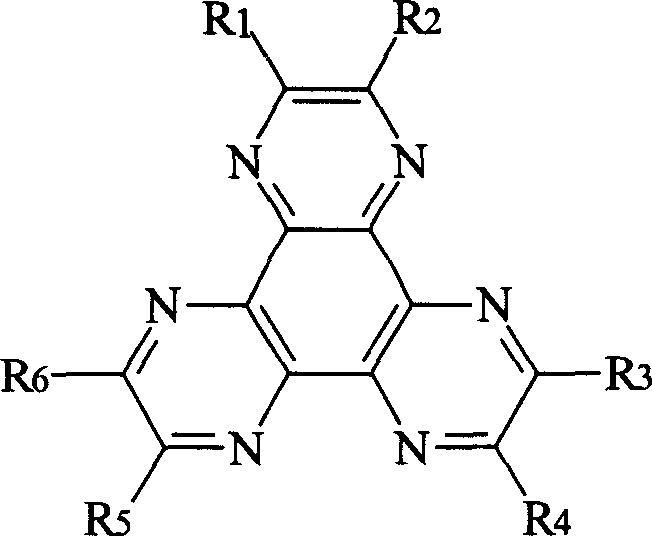
化学式Ichemical formula I
在化学式I中,R1-R6独立地选自包含氢,卤素,腈(-CN),硝基(-NO2),磺酰基(-SO2R),亚砜(-SOR),磺酰胺(-SO2NR),磺酸酯基(-SO3R),三氟甲基(-CF3),酯(-CO-OR),酰胺(-CO-NHR或-CO-NRR’),直链或支化(取代或未取代)C1-C12烷氧基,直链或支化(取代或未取代)C1-C12烷基,芳族或非芳族(取代或未取代)杂环,取代或未取代芳基,单或二(取代或未取代)芳基胺,和(取代或未取代)烷基-(取代或未取代)芳基胺的组。在上述取代基中,R和R’是,例如,取代或未取代C1-C60烷基,取代或未取代芳基,取代或未取代5-7元杂环。取代C1-C60烷基,芳基和杂环任选被一个或多个胺,酰胺,醚和酯基取代。或者,R1-R6独立地选自包含取代或未取代吸电子取代基,这是本领域那些普通技术人员所充分理解的。芳基包括苯基,联苯基,三联苯基,苄基,萘基,蒽基,并四苯基,并五苯基,二萘嵌苯基和晕苯基,它们是单取代或多取代的,或是未取代的。In formula I, R1-R6 are independently selected from hydrogen, halogen, nitrile (-CN), nitro (-NO 2 ), sulfonyl (-SO 2 R), sulfoxide (-SOR), sulfonamide ( -SO 2 NR), sulfonate (-SO 3 R), trifluoromethyl (-CF 3 ), ester (-CO-OR), amide (-CO-NHR or -CO-NRR'), straight Chain or branched (substituted or unsubstituted) C 1 -C 12 alkoxy, straight chain or branched (substituted or unsubstituted) C 1 -C 12 alkyl, aromatic or non-aromatic (substituted or unsubstituted) Groups of heterocycles, substituted or unsubstituted aryls, mono or di(substituted or unsubstituted) arylamines, and (substituted or unsubstituted) alkyl-(substituted or unsubstituted) arylamines. Among the above substituents, R and R' are, for example, substituted or unsubstituted C 1 -C 60 alkyl, substituted or unsubstituted aryl, substituted or unsubstituted 5-7 membered heterocycle. Substituted C 1 -C 60 alkyl, aryl and heterocycles are optionally substituted with one or more amine, amide, ether and ester groups. Alternatively, R1-R6 are independently selected from substituents comprising substituted or unsubstituted electron-withdrawing substituents, which are well understood by those of ordinary skill in the art. Aryl groups include phenyl, biphenyl, terphenyl, benzyl, naphthyl, anthracenyl, naphthacene, pentacene, perylene, and coronene, which are mono- or polysubstituted , or not replaced.
化学式I化合物的非限制性实例如以下化学式Ia-化学式If所示。Non-limiting examples of compounds of Formula I are shown in Formula Ia-If below.
化学式Ia 化学式IbChemical formula Ia Chemical formula Ib
化学式Ic 化学式IdChemical formula Ic Chemical formula Id
化学式Ie 化学式IfChemical formula Ie Chemical formula If
在U.S.专利申请公开No.US2002/0158242A1,以及U.S.专利申请公开No.US6436559和4780536中进一步公开了化学式I的其他实例,这些化合物的合成和化合物的各种特征,所有这些由此在本文中全面引入供参考。Further examples of Formula I, the synthesis of these compounds and the various characteristics of the compounds are further disclosed in U.S. Patent Application Publication No. US2002/0158242A1, and U.S. Patent Application Publication Nos. US6436559 and 4780536, all of which are hereby fully incorporated herein Introduced for reference.
在本发明的一个实施方案中,有机EL器件10包括至少一种化学式Ia-If的化合物。任选地,至少一种化学式Ia-If的化合物单独或与一种或多种化学式I的化合物或其他化合物结合包含在任何上述层中。还任选地,在有机EL器件10的至少一层中单独或与一种或多种其他化合物结合含有化学式Ia的化合物,所述其他化合物可以是或不是用化学式I表示的化合物。In one embodiment of the present invention,
一般,化学式I的化合物可以用于有机EL器件10的任何功能层或多功能层。任选地,该化合物是化学式Ia-If的化合物。任选地,在接触阳极3的任何一层中含有用化学式I表示的一种或多种化合物。在一个实施方案中,有机EL器件包括如图1-3所示的空穴注入层5,且在该空穴注入层5中含有至少一种用化学式I表示的化合物。任选地,空穴注入层用基本不含其他材料的至少一种化学式I表示的化合物形成。或者,空穴注入层用至少一种化学式I表示的化合物与一种或多种其他材料结合来形成。In general, the compound of formula I can be used in any functional or multifunctional layer of the
在另一个实施方案中,有机EL器件包括如在图1-5中所示的空穴传输层7,且在空穴传输层7中含有至少一种用化学式I表示的化合物。任选地,该化合物是化学式Ia-If的化合物。任选地,空穴传输层用或者基本不含其他材料,或者与一种或多种其他材料结合的混合物的至少一种化学式I的化合物形成。在另一个实施方案中,有机EL器件包括具有包括空穴注入和空穴传输的功能的层,该多功能层含有至少一种用化学式I表示的化合物。该多功能层用或者基本不含其他材料,或者与一种或多种其他材料结合的至少一种化学式I的化合物形成。In another embodiment, an organic EL device includes a
虚电极virtual electrode
本发明的另一个方面涉及在包括有机EL器件的电子装置的操作中虚电极的形成。术语“虚电极”是指在电子器件的内部区域中的电荷载流子蓄积,这时它从实电极的角度看起来象电极。虚电极增强或促进了载流子从实电极注入。Another aspect of the present invention relates to the formation of dummy electrodes in the operation of electronic devices including organic EL devices. The term "virtual electrode" refers to the accumulation of charge carriers in an interior region of an electronic device when it appears as an electrode from the perspective of a real electrode. The dummy electrodes enhance or facilitate carrier injection from the real electrodes.
现在参照图7的示例性有机EL器件16的结构来论述虚电极的形成。虽然该论述是针对EL器件,但虚电极不是仅仅在有机EL器件中独有的现象,而是能够在任何其他电子器件中出现。有机EL器件16包括相对设置的阳极3和阴极15。各电极3和15用控制开关19连接于电源17。第一层21和第二层23在对置的电极3和15之间插入。第一层21和第二层23至少其一含有发光材料。The formation of the dummy electrodes will now be discussed with reference to the structure of the exemplary
不希望受本发明如何起作用的任何理论的制约,在一个实施方案中,第一层21由还原状态比中性状态更稳定的材料制成。这里,如果材料自发地由其还原状态转变为其中性状态,那么该材料的还原状态比其中性状态更稳定。进一步推测,例如,电子在第一层21的材料中具有非常低的迁移率,而空穴在其中具有高迁移率。当阳极与第一层21形成接触时,自由电子被传递到第一层21并用于第一层21的材料的还原。因为在该材料中的电子迁移率低,所以传递的电子在跨越阳极3和第一层21之间的边界27之后很难在第一层21内移动。而是,传递的电子停留在第一层21的一侧的边界27附近。因而,从阳极3传递到第一层21的电子沿着边界27蓄积,如附图标记25所示那样。Without wishing to be bound by any theory of how the invention works, in one embodiment,
从阳极3的观点来看,沿边界27的蓄积的电子或负电荷被看作好像是电子源,即器件的阴极,与边界27非常接近,因负电荷非常丰富。在该意义上,蓄积电子25的区域被称为虚阴极。当通过操作开关19在电极3和15之间施加正向偏压时,阳极3将空穴注入虚阴极25并因此注入第一层21。虚阴极的负电荷与阳极3的接近有利于从阳极3注入空穴。借助由阳极3的注入的动力和在两个电极3和15之间的正向偏压,注入到第一层21的空穴向实阴极15或第二层23的方向前进。第一层21的材料的高空穴迁移率有助于空穴沿向实阴极15或第二层23的方向传输。From the point of view of the
类似的现象可以发生在第二层23中,以通过空穴沿阴极15和第二层23之间的边界29的蓄积形成虚阳极。第二层23的材料选自其氧化状态比其中性状态更稳定,并且具有低空穴迁移率和高电子迁移率的那些化合物。空穴从阴极15传递到第二层23并在阴极15和第二层23之间的边界附近蓄积。从阴极15的角度来看,蓄积的空穴被当作虚阳极。在施加适当的正向偏压电能时,阴极15将电子注入到第二层23中。A similar phenomenon may occur in the
根据本发明的各个实施方案,电荷载流子在器件的内部区域中蓄积以形成虚电极。在有机EL器件16(图7)中,例如,第一层21可以构成空穴注入层、空穴传输层、发光层或具有上述层的功能的多功能层。或者,第一层可以不存在,而阳极3接触第二层23。第二层23可以构成,例如,空穴传输层、发光层、电子传输层、电子注入层或具有上述层的一种或多种功能的多功能层。或者,第二层23可以不存在,而阴极15与第一层21接触。虽然根据具有层21和23的一层或二层的有机EL器件论述了该现象,但同样的情况在有机EL器件的任何其他结构中,例如在阳极3和阴极15之间插入两层以上层的结构中也适用。According to various embodiments of the invention, charge carriers accumulate in the interior region of the device to form dummy electrodes. In the organic EL device 16 (FIG. 7), for example, the
在形成虚电极的有机EL器件的实施方案中,第一层21含有其还原状态比其中性状态更稳定的化合物。任选地,这种化合物选自用化学式I表示的化合物。优选地,第一层含有化学式Ia的化合物。在另一个实施方案中,第一层21的化合物具有大约-0.6伏(V)到大约0V,优选大约-0.2V到大约0V的还原电位。或者,第一层21的化合物的还原电位是大约-0.3V到大约0V,任选大约-0.1V到大约0V。第一层21含有化合物,在其中,电子具有低迁移率,而空穴具有高迁移率。第一层21的化合物具有等于或低于大约10-5cm/V.s,优选大约10-10cm/V.s到大约10-6cm/V.s的电子迁移率。第一层21的化合物具有等于或高于大约10-4cm/V.s,优选大约10-4cm/V.s到大约1cm/V.s的空穴迁移率。In an embodiment of an organic EL device forming a dummy electrode, the
在形成虚电极的有机EL器件的实施方案中,第二层23含有其氧化状态比其中性状态更稳定的化合物。在另一个实施方案中,第二层23含有具有等于或低于大约0.5V的氧化电位的第二层23的化合物。或者,该化合物的氧化电位是大约0到大约0.4V,优选大约0到大约0.3V。第二层23含有其中空穴具有低迁移率,而电子具有高迁移率的化合物。第二层23的化合物具有等于或低于大约10-4cm/V.s,优选大约10-10cm/V.s到大约10-5cm/V.s的空穴迁移率。第二层23的化合物具有等于或高于大约10-5cm/V.s,优选大约10-5cm/V.s到大约1cm/V.s的电子迁移率。In an embodiment of an organic EL device forming a dummy electrode, the
电极材料的功函数Work function of electrode material
本发明的另一个方面涉及在阳极3中使用具有低功函数的材料。相关领域的常识是,阳极的材料选自具有相对高的功函数的那些材料;另一方面,阴极的材料选自具有相对低的功函数的那些材料。然而,根据本发明的一个实施方案,有机EL器件具有其材料具有相对低的功函数的阳极。例如阳极材料的功函数低于大约4.5eV,优选低于大约4.3eV。或者,阳极材料的功函数是大约3.5eV到大约4.5eV,优选大约3.8eV到大约4.3eV。在阳极中使用的材料包括,例如,铝(Al,4.28eV),银(Ag,4.26eV),锌(Zn,4.33eV),铌(Nb,4.3eV),锆(Zr,4.05eV),锡(Sn,4.42eV),钽(Ta,4.25eV),钒(V,4.3eV),汞(Hg,4.49eV),镓(Ga,4.2eV),铟(In,4.12eV),镉(Cd,4.22eV),硼(B,4.4eV),铪(Hf,3.9eV),镧(La,3.5eV),铌(Nb,4.3eV),钛(Ti,4.3eV)或上述金属之一与钕(Nd)或钯(Pd)的合金。Another aspect of the invention relates to the use of materials with a low work function in the
相对低功函数的材料在阳极中的使用的一种可能的、但非限制性的解释是:低功函数阳极材料有助于形成上述虚阴极。回头参看图7,在形成阳极3和第一层21之间的接触时,阳极3的低功函数材料容易将电子传递到第一层21。在施加适当的电压时,增强了从阳极3到第一层21的电子传递。传递到第一层21的电子形成了虚阴极25,这增强了如上所述的空穴以朝向实阴极15的方向从阳极3注入到第一层21中。One possible, but non-limiting, explanation for the use of relatively low work function materials in the anode is that the low work function anode material contributes to the formation of the aforementioned virtual cathode. Referring back to FIG. 7 , when the contact between the
根据本发明的一个实施方案,阴极材料的功函数低于大约4.5eV。用于阴极15的材料包括,例如,镁,钙,钠,钾,钛,铟,钇,锂,钆,铝,银,锡,铅,类似金属,CsF,含有一种或多种上述金属的合金,或含有一种或多种上述金属的多层,包括LiF/Al和Li2O/Al。透明或不透明材料可以被用于阴极15,取决于在如上所述的有机EL器件中的光路(light passage)的结构。本领域的那些普通技术人员很清楚能够在阴极15中使用的任何其他材料以及适当阴极材料的选择。According to one embodiment of the invention, the work function of the cathode material is below about 4.5 eV. Materials for
根据本发明的一个实施方案,阳极3具有由单一材料形成的单层结构,可以是基本纯的元素材料,或均相或非均相合金。在另一个实施方案中,阳极3可以包括多个亚层,它们可以包括或不包括非导电亚层。任选地,以上阳极材料的功函数的论述仅仅适用于阳极3的导电部件,不适用于其非导电亚层或部件。任选地,阳极3可以具有一个或多个导电材料压层。在包括多个导电材料亚层的阳极结构的情况下,以上阳极材料的功函数的论述适用于至少一种导电材料。According to one embodiment of the invention, the
本发明的另一个方面涉及具有高功函数的材料在阴极15中的用途。恰好象低功函数阳极一样,高功函数阴极材料有助于形成上述虚阳极。根据本发明的一个实施方案,有机EL器件10具有阴极15,它的材料具有高功函数。例如,阴极材料的功函数是在大约3.5eV以上,优选在大约4eV以上。或者,阴极材料的功函数是大约4.1eV到大约5.0eV,优选大约4.1eV到大约4.8eV。Another aspect of the invention relates to the use of a material with a high work function in the
阳极的反射材料reflective material for the anode
本发明的另一个方面涉及反射材料在有机EL器件的阳极3中的应用。在根据本发明的有机EL器件的一个实施方案中,阳极用一种或多种具有高反射率的材料形成。例如,作为反射光强度与入射光强度的比率的反射率是在大约0.2以上,例如大约0.4到大约1。用于阳极3的反射材料包括,例如,铝,银,金,镍,铬,钼,钽,钛,和锌。任选地,这些材料可反射可见光的基本上所有波长成分。任选地,这些材料对可见光的基本所有波长成分具有基本均匀的反射率。优选的是,反射阳极材料是,例如,铝,银,铂,铬和镍。Another aspect of the invention relates to the use of reflective materials in the
在本发明的一个实施方案中,阳极3可以包括多个亚层。任选地,阳极3可以由至少一透明亚层和反射亚层形成。该至少一透明亚层可以用透明材料形成,例如透明材料包括ITO(氧化铟锡),IZO(氧化铟锌),和氟化锡氧化物。反射亚层用如上所述的一种或多种反射材料形成。作为选择方案,阳极3是由反射材料制成的单层。从制造工艺的简单性来看,阳极的该单层结构比多个亚层结构有利。In one embodiment of the invention, the
顶部发射top launch
在阳极3,而非阴极15,接触基层1的图1-6的结构中,在阳极3中使用反射材料使得所产生的光可以通过阴极15发射或沿除了通过阳极3以外的方向发射。在图1-6的相同结构中,通过阴极的15发射被称为顶部发射;另一方面,通过阳极3和基层1的发射被称为底部发射。任选地,有机EL器件10可以按顶部发射方式构造。对于顶部发射,阴极15是基本透明的。In the structures of FIGS. 1-6 where the
在一个实施方案中,在一种或多种透明导电材料的单一层中形成基本透明的阴极15。透明导电材料的实例包括ITO(氧化铟锡),IZO(氧化铟锌),和氟化锡氧化物。或者,基本透明的阴极15形成多层(未示出)。例如,多层结构的阴极15可以包括由通常非透明材料形成的薄层和透明材料层。通常非透明材料的薄层以能够透过从有机EL材料发射的可见光的厚度形成。任选地,薄层的厚度是大约10到大约500,优选大约10到大约200。用于薄层的通常非透明材料包括,例如,镁(Mg),钙(Ca),锂(Li),铝(Al),铟(In),钾(K),钇(Y),锶(St),铕(Eu),钠(Na),镓(Ga),钐(Sm),或者两种或多种上述元素的合金或混合物。该透明材料层由一种或多种材料制成,例如是氧化铟锡(ITO),氧化铟锌(IZO),和氟化锡氧化物。透明材料层的厚度是大约100到大约5000。多层结构的阴极15可以进一步包括一个或多个附加层。In one embodiment, the substantially
控制电路的位置和类型Location and type of control circuit
与底部发射设计相比,有机EL器件的顶部发射设计通常与该器件的有源矩阵驱动更相适应。如图8所示,有源矩阵驱动需要在基层1和阳极3之间的用于晶体管或集成电路的层31。在具有底部发射设计的有机EL器件中,集成电路层31将阻挡由发光化合物发出的至少一些光。然而顶部发射设计不会受到在阳极3下面的集成电路层31的存在的影响。顶部发射设计也不会受到形成集成电路层31的技术的影响,例如使用非晶硅或多晶硅的集成电路层31影响层31的孔径比。A top emitting design for an organic EL device is generally more compatible with active matrix driving of the device than a bottom emitting design. Active matrix driving requires a layer 31 between the
在顶部发射设计的实施方案中,有机EL器件利用无源矩阵或有源矩阵电路设计。任选地,顶部发射设计利用有源矩阵电路设计。还任选的是,有源矩阵驱动的集成电路在基层1和阳极3之间形成。还任选的是,用非晶硅技术形成集成电路。In an embodiment of a top emission design, the organic EL device utilizes a passive matrix or active matrix circuit design. Optionally, the top-emitting design utilizes an active matrix circuit design. Also optionally, an active matrix driven integrated circuit is formed between the
密封层sealing layer
在有机EL器件的某些实施方案中,有利的是,在基层1和阳极3之间具有密封层,以防止水分或其他污染物质渗透到层状结构的复杂区域。尤其当基层1的材料的渗透性高时,这种密封层更加重要。密封层常常用一种或多种基本不透性材料或半透性材料制备。这种材料例如是铝,氧化铝,氧化锶,氧化钡,氧化硅,氮化硅。密封层可以构造成多层,包括至少一有机亚层和至少一无机亚层的。有机亚层可以用,例如,聚苯乙烯、聚合环氧化合物和/或聚环烷烃形成。无机亚层可以用,例如,氮化硅、氧化硅和/或氧化钡形成。就基本不透性或半透性的材料也能够用作阳极材料而言,阳极3本身形成了密封层。因此,不需要形成单独的密封层。在本发明的一个实施方案中,阳极3由铝,铝-钕合金或铝-钯合金制成,它们也起密封层的作用。也起密封层的作用的阳极3与任何适当的基层一起使用,在基层1和阳极3之间的插入或不插入集成电路层31。In some embodiments of the organic EL device, it is advantageous to have a sealing layer between the
阳极的非导电亚层Non-conductive sublayer of the anode
在本发明的任何有机EL器件实施方案中,阳极3和阴极15的任何一个或两个可以以多个亚层形成。参看图9,例如,所示有机EL器件的阳极3包括导电亚层33和非导电亚层35。虽然用两个亚层示出,但阳极3可以具有两个以上的亚层。如图所示,非导电亚层35位于导电亚层33和空穴注入层5之间,空穴注入层5在阳极3朝向阴极15的一侧与阳极3接触。在该层状阳极结构中的空穴注入层5能够替代空穴传输层7(图4和5),发光层9(图6)或多功能层7(未示出)。在可供选择的实施方案中,非导电亚层35可以被认为是在阳极3和接触阳极3的层5、7或9之间插入的单独层。In any of the organic EL device embodiments of the present invention, either or both of the
作为单独层考虑,非导电亚层35可以被称为缓冲层。不管其名称如何,形成非导电亚层或缓冲层35,以便改进导电亚层33(或阳极3)和接触阳极3的层5、7或9之间的界面强度。非导电亚层或缓冲层35还有助于降低空穴从导电亚层33注入到接触非导电亚层35的层5、7或9中的能障。在一个实施方案中,非导电亚层或缓冲层35用一种或多种无机材料形成。任选地,缓冲层的材料包括,例如,氧化铝,氧化钛,氧化锌,氧化钌,氧化镍,氧化锆,氧化钽,氧化镁,氧化钙,氧化锶,氧化钒,氧化钇,氧化锂,氧化铯,氧化铬,氧化硅,氧化钡,氧化锰,氧化钴,氧化铜,氧化镨,氧化钨,氧化锗,氧化钾,氟化锂,氟化镁,氟化铯,氟化钙,氯化钠,氯化钾,偏硼酸锂(BiBO2),硅酸钾(K2SiO3),氧化硅-锗,钛酸钡,钽酸锂(LiTaO3),氮化硅(Si3N4),氮化硼(BN),元素周期表的III或IV族中的元素的氮化物,硫化锌(ZnS),硫化镉(CdS),硒化镉(CdSe),磷化稼(GaP),氮化镓(GaN),以及两种或多种上述材料的组合物。Considered as a separate layer, the
器件的制造device manufacturing
本发明的有机EL器件的各层能够通过利用任何成膜技术(包括溅射,电子束蒸汽沉积,其他类型的物理蒸汽沉积(PVD),化学蒸汽沉积(CVD),旋涂,浸涂,刮涂,喷墨印刷,丝网印刷,辊涂和热传递)来生产。这些技术概括地描述在以下出版物中,它们由此在这里引入供参考:Applied Physics Letters,73,18,1998,2561-2563;AppliedPhysics Letters,78,24,2001,3905-3907。本领域的普通技术人员应知道在用于形成这些层的条件和情况下的适当成膜技术。Each layer of the organic EL device of the present invention can be formed by utilizing any film-forming technique (including sputtering, electron beam vapor deposition, other types of physical vapor deposition (PVD), chemical vapor deposition (CVD), spin coating, dip coating, scraping coating, inkjet printing, screen printing, roll coating and heat transfer) to produce. These techniques are broadly described in the following publications, which are hereby incorporated by reference: Applied Physics Letters, 73, 18, 1998, 2561-2563; Applied Physics Letters, 78, 24, 2001, 3905-3907. Those of ordinary skill in the art will know appropriate film-forming techniques under the conditions and circumstances used to form these layers.
实施例Example
以下通过实施例来进一步描述本发明的各个方面和特征。以下实施例用来举例说明本发明的各个方面和特征,但不限制本发明的范围。Various aspects and features of the present invention are further described through examples below. The following examples serve to illustrate various aspects and features of the invention, but do not limit the scope of the invention.
实施例1Example 1
玻璃基层(Coming 7059)涂布大约1300氧化铟锡(ITO),并在购自Fischer Co.的清洁剂的水溶液中进行超声清洗。干燥清洗的形成ITO层的基层,再转移到等离子体清洁设备中。该基层进一步用氩-氧(2∶1)等离子体在5W和14毫托下清洗5分钟。然后将基层转移到真空蒸汽沉积室中。A glass substrate (Coming 7059) was coated with approximately 1300 Å indium tin oxide (ITO) and ultrasonically cleaned in an aqueous solution of cleaner from Fischer Co. The cleaned substrate forming the ITO layer is dried and transferred to a plasma cleaning device. The substrate was further cleaned with argon-oxygen (2:1) plasma at 5 W and 14 mTorr for 5 minutes. The base layer is then transferred into a vacuum vapor deposition chamber.
通过热真空蒸汽沉积在ITO层上沉积大约100的铝层,以便形成半透明的铝阳极。该铝层在大气压下接触氧气5分钟,以形成大约20的氧化铝层。在该氧化铝层上通过热真空沉积形成大约500的化学式Ia的化合物(六腈六氮杂三亚苯基或HAT)的空穴注入层。在该空穴注入层上,通过热真空沉积用NPB形成大约400的空穴传输层。在该空穴传输层上,通过热真空沉积用Alq3形成大约300的发光层。在该发光层上,通过热真空沉积用化学式II的化合物(2-([4-[(N-苯基苯并咪唑-2-基)苯基-9,10-双(2-萘基)蒽]形成大约200的电子传输层。对于阴极,在该电子传输层上形成大约10的氟化锂(LiF)层,然后进一步沉积大约2500铝层。在沉积过程中,沉积室内的压力保持在5-8×10⁻⁷托。有机材料以1/sec的速度沉积。氟化锂以0.3/sec的速度沉积,以及铝以3-7/sec的速度沉积。An aluminum layer of approximately 100 A was deposited on the ITO layer by thermal vacuum vapor deposition to form a translucent aluminum anode. The aluminum layer was exposed to oxygen at atmospheric pressure for 5 minutes to form an aluminum oxide layer of about 20 A. A hole injection layer of about 500 Å of the compound of formula Ia (hexanitrile hexaazatriphenylene or HAT) was formed on the aluminum oxide layer by thermal vacuum deposition. On this hole injection layer, a hole transport layer of about 400 Ȧ was formed with NPB by thermal vacuum deposition. On this hole transport layer, a light emitting layer of about 300 Ȧ was formed with Alq3 by thermal vacuum deposition. On this light-emitting layer, the compound (2-([4-[(N-phenylbenzimidazol-2-yl)phenyl-9,10-bis(2-naphthyl) Anthracene] forms an electron transport layer of about 200 Ȧ. For the cathode, a lithium fluoride (LiF) layer of about 10 Ȧ is formed on the electron transport layer, and then an aluminum layer of about 2500 Ȧ is further deposited. During the deposition process, the deposition chamber The pressure was maintained at 5-8

化学式IIchemical formula II
有机EL器件的所得层状结构表示为“玻璃基层/ITO(1300)/Al(100)/Al2O3(20)/HAT(500)/NPB(400)/Alq3(300)/化学式II(200)/LiF(10)/Al(2500)”。当在所得器件两端上施加5.17V的正向偏压时,通过半透明铝层观察到500nit的发光。发光的颜色在1931 CIE色坐标中被确定为x=0.460,y=0.550。在操作过程中的电流密度为50mA/cm2。The resulting layered structure of the organic EL device is expressed as "glass-based layer/ITO (1300 Ȧ)/Al (100 Ȧ)/Al 2 O 3 (20 Ȧ)/HAT (500 Ȧ)/NPB (400 Ȧ)/Alq3 (300 Ȧ Ȧ)/chemical formula II (200 Ȧ)/LiF (10 Ȧ)/Al (2500 Ȧ)". When a forward bias of 5.17 V was applied across the resulting device, luminescence of 500 nit was observed through the semitransparent aluminum layer. The color of the emission was determined in the 1931 CIE color coordinates as x=0.460, y=0.550. The current density during operation was 50 mA/cm 2 .
实施例2Example 2
按照与实施例1相同的方式制造器件,只是不形成ITO层和不形成Al2O3层。所得结构表示为“玻璃基层/Al(100)/HAT(500)/NPB(400)/Alq3(300)/化学式II(200)/LiF(10)/Al(2500)”。A device was fabricated in the same manner as in Example 1 except that no ITO layer was formed and no Al2O3 layer was formed. The resulting structure is expressed as "glass-based layer/Al(100A)/HAT(500A)/NPB(400A)/Alq3(300A)/chemical formula II(200A)/LiF(10A)/Al(2500A) ".
当在所得器件两端施加5.0V的正向偏压时,通过半透明铝层观察到1,010nit的发光。发光的颜色在1931CIE色坐标中被确定为x=0.417,y=0.534。在操作过程中的电流密度为50mA/cm2。When a forward bias of 5.0 V was applied across the resulting device, luminescence of 1,010 nit was observed through the semitransparent aluminum layer. The color of the emission was determined in 1931 CIE color coordinates as x=0.417, y=0.534. The current density during operation was 50 mA/cm 2 .
实施例3Example 3
按照与实施例1相同的方式制造器件,只是不形成HAT的空穴注入层。器件的所得结构表示为“玻璃基层/ITO(1300)/Al(100)/Al2O3(20)/NPB(400)/Alq3(300)/化学式II(200)/LiF(10)/Al(2500)”。即使当对该器件施加超过20V的正向偏压时,也没有发现发光。在施加正向偏压的过程中的电流密度小于0.1mA/cm2。A device was fabricated in the same manner as in Example 1 except that the hole injection layer of the HAT was not formed. The resulting structure of the device is expressed as "Glass-Based/ITO(1300A)/Al(100A)/ Al2O3 ( 20A )/NPB(400A)/Alq3(300A)/Chemical Formula II(200A)/ LiF(10A)/Al(2500A)". Even when a forward bias exceeding 20 V was applied to the device, no light emission was found. The current density during application of the forward bias is less than 0.1 mA/cm 2 .
实施例4Example 4
按照与实施例1相同的方式制造器件,只是不形成在ITO和NPB之间的铝层和氧化铝层。所得结构表示为“玻璃基层/ITO(1300)/HAT(500)/NPB(400)/Alq3(300)/化学式II(200)/LiF(10)/Al(2500)”。当在所得器件两端施加5.37V的正向偏压时,观察到1931CIE色坐标的颜色x=0.345,y=0.553的绿色发光。在操作过程中的电流密度为50mA/cm2。在100mA/cm2的恒定DC电流密度下,到3399nit的初始亮度下降到80%水平的亮度时用了23小时。A device was fabricated in the same manner as in Example 1 except that the aluminum layer and aluminum oxide layer between ITO and NPB were not formed. The resulting structure is expressed as "glass-based layer/ITO (1300 Ȧ)/HAT (500 Ȧ)/NPB (400 Ȧ)/Alq3 (300 Ȧ)/chemical formula II (200 Ȧ)/LiF (10 Ȧ)/Al (2500 Ȧ) ". When a forward bias voltage of 5.37 V was applied across the resulting device, green emission with a color x=0.345, y=0.553 of 1931 CIE color coordinates was observed. The current density during operation was 50 mA/cm 2 . At a constant DC current density of 100mA/cm 2 , it took 23 hours to drop from the initial brightness of 3399 nit to 80% level brightness.
实施例5Example 5
按照与实施例1相同的方式制造器件,只是形成作为半透明阳极的为100厚度的银层,代替铝和氧化铝层。所得器件的结构表示为“玻璃基层/ITO(1300)/Ag(100)/HAT(500)/NPB(400)/Alq3(300)/化学式II(200)/LiF(10)/Al(2500)”。当在所得器件两端施加5.1V的正向偏压时,观察到1931 CIE色坐标的颜色x=0.420,y=0.516的800nit的发光。在操作过程中的电流密度为50mA/cm2。A device was fabricated in the same manner as in Example 1, except that a silver layer was formed as a semitransparent anode with a thickness of 100 Ȧ instead of the aluminum and aluminum oxide layers. The structure of the obtained device is expressed as "glass base layer/ITO (1300 Ȧ)/Ag (100 Ȧ)/HAT (500 Ȧ)/NPB (400 Ȧ)/Alq3 (300 Ȧ)/chemical formula II (200 Ȧ)/LiF (10 Ȧ A)/Al (2500A)". When a forward bias voltage of 5.1 V was applied across the resulting device, 800 nit luminescence with a color x=0.420, y=0.516 of 1931 CIE color coordinates was observed. The current density during operation was 50 mA/cm 2 .
实施例6Example 6
按照与实施例5相同的方式制造器件,只是不形成ITO层。所得结构表示为“玻璃基层/Ag(100)/HAT(500)/NPB(400)/Alq3(300)/化学式II(200)/LiF(10)/Al(2500)”。当在所得器件两端施加正向偏压时,观察到可见光。A device was fabricated in the same manner as in Example 5 except that the ITO layer was not formed. The resulting structure is expressed as "glass-based layer/Ag(100A)/HAT(500A)/NPB(400A)/Alq3(300A)/chemical formula II(200A)/LiF(10A)/Al(2500A) ". When a forward bias voltage was applied across the resulting device, visible light was observed.
实施例7Example 7
玻璃基层(Coming 7059)涂布大约1300氧化铟锡(ITO),并在购自Fischer Co.的清洁剂的水溶液中进行超声清洗。干燥清洗的具有ITO层的基层,再转移到等离子体清洁设备中。该基层进一步用氩-氧(2∶1)等离子体在5W和14毫托下清洗5分钟。然后将基层转移到真空蒸汽沉积室中。A glass substrate (Coming 7059) was coated with approximately 1300 Å indium tin oxide (ITO) and ultrasonically cleaned in an aqueous solution of cleaner from Fischer Co. The cleaned substrate with the ITO layer is dried and transferred to a plasma cleaning device. The substrate was further cleaned with argon-oxygen (2:1) plasma at 5 W and 14 mTorr for 5 minutes. The base layer is then transferred into a vacuum vapor deposition chamber.
通过热真空蒸汽沉积在ITO层上沉积大约2000的化学式Ia的化合物(六腈六氮杂三亚苯基或HAT)。在该化合物层上,沉积大约500铝,以形成阴极。在沉积过程中,沉积室内的压力保持在5-8×10⁻⁷托。有机材料以1/sec的速度沉积,而铝以3-7/sec的速度沉积。About 2000 Å of the compound of formula Ia (hexanitrile hexaazatriphenylene or HAT) was deposited on the ITO layer by thermal vacuum vapor deposition. On this compound layer, about 500 Å of aluminum is deposited to form the cathode. During the deposition process, the pressure in the deposition chamber was maintained at 5-8
有机EL器件的所得层状结构表示为“玻璃基层/ITO(1300)/HAT(2000)/Al(500)”。当在所得器件两端施加正向偏压时,刚好在0V以上的电位差下观察到电流。电压-电流关系曲线在图10中示出。The resulting layered structure of the organic EL device is expressed as "glass-based layer/ITO (1300 Å)/HAT (2000 Å)/Al (500 Å)". When a forward bias was applied across the resulting device, current flow was observed at potential differences just above 0 V. The voltage-current relationship is shown in FIG. 10 .
实施例8Example 8
按照与实施例7相同的方式制造器件,只是形成1600厚度的NPB代替HAT。所得器件的结构表示为“玻璃基层/ITO(1300)/NPB(1600)/Al(500)”。当在所得器件两端施加正向偏压时,在大约1V的电位差下观察到电流。电压-电流关系曲线也在图10中示出。A device was fabricated in the same manner as in Example 7, except that NPB was formed to a thickness of 1600 Ȧ instead of HAT. The structure of the resulting device is expressed as "glass-based/ITO(1300A)/NPB(1600A)/Al(500A)". When a forward bias was applied across the resulting device, current flow was observed at a potential difference of approximately 1 V. The voltage-current relationship is also shown in FIG. 10 .
实施例9Example 9
按照与实施例7相同的方式制造器件,只是形成作为阳极的500铝层代替ITO层。所得结构表示为“玻璃基层/Al(500)/HAT(2000)/Al(500)”。当在所得器件两端施加正向偏压时,在刚好0V以上的电位差下观察到电流。电压-电流关系曲线在图11中示出。A device was fabricated in the same manner as in Example 7, except that a 500 Ȧ aluminum layer was formed as an anode instead of the ITO layer. The resulting structure is expressed as "glass-based layer/Al(500A)/HAT(2000A)/Al(500A)". When a forward bias was applied across the resulting device, current flow was observed at potential differences just above 0 V. The voltage-current relationship is shown in FIG. 11 .
实施例10Example 10
按照与实施例9相同的方式制造器件,只是形成2000厚度的NPB代替HAT。所得器件结构表示为“玻璃基层/Al(500)/NPB(2000)/Al(500)”。当在所得器件两端施加正向偏压时,即使在超过20V的电位差下也没有观察到电流。电压-电流关系曲线也在图11中示出。A device was fabricated in the same manner as in Example 9, except that NPB was formed to a thickness of 2000 Ȧ instead of HAT. The resulting device structure is denoted as "glass-based layer/Al(500A)/NPB(2000A)/Al(500A)". When a forward bias was applied across the resulting device, no current flow was observed even at a potential difference exceeding 20 V. The voltage-current relationship is also shown in FIG. 11 .
实施例11Example 11
对于具有“玻璃基层/Al(500)/HAT(2000)/Al(500)”的结构的在实施例9中制造的器件,用与实施例9相反的极性施加电位,其中位于玻璃基层和HAT层之间的铝用作阴极,以及位于HAT以上的铝用作阳极。在施加正向偏压时,电流开始刚好在0V以上开始流动。电压-电流关系曲线还在图12中示出。该结果与实施例9的结果结合表明,HAT层能使铝层将空穴注入到其中,无论铝层是沉积在HAT层之下,还是HAT层之上。For the device fabricated in Example 9 having the structure of "glass-based layer/Al (500 Å)/HAT (2000 Å)/Al (500 Å)", a potential was applied with the opposite polarity to that of Example 9, where The aluminum between the glass base layer and the HAT layer was used as the cathode, and the aluminum above the HAT was used as the anode. On applying a forward bias, current begins to flow just above 0V. The voltage-current relationship is also shown in FIG. 12 . This result, combined with the results of Example 9, shows that the HAT layer enables the aluminum layer to inject holes into it, regardless of whether the aluminum layer is deposited below or above the HAT layer.
实施例12Example 12
对于具有“玻璃基层/Al(500)/NPB(2000)/Al(500)”的结构的在实施例10中制造的器件,用与实施例10相反的极性施加电位,其中位于玻璃基层和NPB层之间的铝用作阴极,以及位于HAT以上的铝用作阳极。在施加正向偏压时,在20V以上的电位差下几乎没有发现电流。电压-电流关系曲线也在图12中示出。For the device fabricated in Example 10 having the structure of "glass-based layer/Al (500 Å)/NPB (2000 Å)/Al (500 Å)", a potential was applied with the opposite polarity to that of Example 10, where The aluminum between the glass base layer and the NPB layer was used as the cathode, and the aluminum above the HAT was used as the anode. Almost no current flow was found at potential differences above 20V when a forward bias was applied. The voltage-current relationship is also shown in FIG. 12 .
Claims (46)


Applications Claiming Priority (2)
| Application Number | Priority Date | Filing Date | Title |
|---|---|---|---|
| KR20020078809 | 2002-12-11 | ||
| KR1020020078809 | 2002-12-11 |
Publications (2)
| Publication Number | Publication Date |
|---|---|
| CN1989787A true CN1989787A (en) | 2007-06-27 |
| CN100527472C CN100527472C (en) | 2009-08-12 |
Family
ID=32501361
Family Applications (1)
| Application Number | Title | Priority Date | Filing Date |
|---|---|---|---|
| CNB2003801000992A Expired - Lifetime CN100527472C (en) | 2002-12-11 | 2003-12-05 | Electroluminescent devices with low work function anode |
Country Status (10)
| Country | Link |
|---|---|
| US (3) | US7560175B2 (en) |
| EP (3) | EP1842891B1 (en) |
| JP (3) | JP4537207B2 (en) |
| KR (1) | KR100606634B1 (en) |
| CN (1) | CN100527472C (en) |
| AT (1) | ATE433649T1 (en) |
| AU (1) | AU2003302867A1 (en) |
| DE (1) | DE60327944D1 (en) |
| TW (1) | TWI241864B (en) |
| WO (1) | WO2004054326A2 (en) |
Cited By (16)
| Publication number | Priority date | Publication date | Assignee | Title |
|---|---|---|---|---|
| CN101826600A (en) * | 2010-04-09 | 2010-09-08 | 苏旋 | Organic electroluminescent diode device |
| CN101978527A (en) * | 2008-01-18 | 2011-02-16 | 阿斯特朗非凡安全有限公司 | Organic light-emitting diode with microcavity including doped organic layers and fabrication process thereof |
| CN102005540A (en) * | 2010-10-12 | 2011-04-06 | 西安文景光电科技有限公司 | Organic electroluminescent device taking metal and P-type disc-shaped compound as composite anode |
| CN102157703A (en) * | 2011-03-03 | 2011-08-17 | 西安文景光电科技有限公司 | OLED (Organic Light Emitting Diode) device for increasing brightness |
| CN102201432A (en) * | 2010-03-08 | 2011-09-28 | 三星移动显示器株式会社 | Organic light-emitting device and method of manufacturing the same |
| CN102544368A (en) * | 2012-02-10 | 2012-07-04 | 中国科学院微电子研究所 | A kind of organic thin film transistor and its preparation method |
| CN103219472A (en) * | 2013-04-19 | 2013-07-24 | 云南北方奥雷德光电科技股份有限公司 | Top-emitting organic light-emitting diode (OLED) device anode structure and preparation technology thereof |
| CN104009166A (en) * | 2013-02-26 | 2014-08-27 | 海洋王照明科技股份有限公司 | Organic electroluminescent device and preparation method |
| CN104009180A (en) * | 2013-02-26 | 2014-08-27 | 海洋王照明科技股份有限公司 | Organic electroluminescent device and preparation method |
| CN104009167A (en) * | 2013-02-26 | 2014-08-27 | 海洋王照明科技股份有限公司 | Organic electroluminescent device and preparation method |
| CN104009162A (en) * | 2013-02-26 | 2014-08-27 | 海洋王照明科技股份有限公司 | Organic electroluminescent device and preparation method |
| CN104183738A (en) * | 2013-05-24 | 2014-12-03 | 海洋王照明科技股份有限公司 | Organic electroluminescent device and preparation method thereof |
| CN104183729A (en) * | 2013-05-24 | 2014-12-03 | 海洋王照明科技股份有限公司 | Organic light emitting device and manufacturing method thereof |
| CN102317408B (en) * | 2009-02-17 | 2015-03-04 | 默克专利有限公司 | Organic electronic device |
| CN110875432A (en) * | 2018-08-31 | 2020-03-10 | 三星显示有限公司 | Organic light emitting device and compound |
| US12532658B2 (en) | 2019-07-26 | 2026-01-20 | Samsung Display Co., Ltd. | Anthracene-based compound and organic light-emitting device including the same |
Families Citing this family (147)
| Publication number | Priority date | Publication date | Assignee | Title |
|---|---|---|---|---|
| KR100377321B1 (en) * | 1999-12-31 | 2003-03-26 | 주식회사 엘지화학 | Electronic device comprising organic compound having p-type semiconducting characteristics |
| KR100721656B1 (en) * | 2005-11-01 | 2007-05-23 | 주식회사 엘지화학 | Organic electrical devices |
| US7560175B2 (en) * | 1999-12-31 | 2009-07-14 | Lg Chem, Ltd. | Electroluminescent devices with low work function anode |
| JP4628690B2 (en) * | 2004-03-24 | 2011-02-09 | 株式会社 日立ディスプレイズ | Organic light emitting display |
| EP1743508B1 (en) | 2004-04-09 | 2012-05-23 | LG Chem, Ltd. | Stacked organic light emitting device having high efficiency and high brightness |
| US7365360B2 (en) | 2004-05-11 | 2008-04-29 | Lg. Chem, Ltd. | Organic electronic device |
| KR101068395B1 (en) * | 2004-06-30 | 2011-09-28 | 엘지디스플레이 주식회사 | An organic light emitting display device having a top emission type and a method of manufacturing the same |
| US7812522B2 (en) * | 2004-07-22 | 2010-10-12 | Ifire Ip Corporation | Aluminum oxide and aluminum oxynitride layers for use with phosphors for electroluminescent displays |
| JP4578215B2 (en) * | 2004-11-30 | 2010-11-10 | 三洋電機株式会社 | Organic electroluminescent device and organic electroluminescent display device |
| JP4565922B2 (en) * | 2004-07-30 | 2010-10-20 | 三洋電機株式会社 | Organic electroluminescent device and organic electroluminescent display device |
| JP4785386B2 (en) * | 2005-01-31 | 2011-10-05 | 三洋電機株式会社 | Organic electroluminescent device and organic electroluminescent display device |
| JP2006066380A (en) * | 2004-07-30 | 2006-03-09 | Sanyo Electric Co Ltd | Organic electroluminescence element and organic electroluminescence display device |
| JP4315874B2 (en) * | 2004-07-30 | 2009-08-19 | 三洋電機株式会社 | Organic electroluminescent device and organic electroluminescent display device |
| JP2006066379A (en) * | 2004-07-30 | 2006-03-09 | Sanyo Electric Co Ltd | Organic electroluminescence element and organic electroluminescence display device |
| JP4434872B2 (en) * | 2004-07-30 | 2010-03-17 | 三洋電機株式会社 | Organic electroluminescent device and organic electroluminescent display device |
| JP4565921B2 (en) * | 2004-07-30 | 2010-10-20 | 三洋電機株式会社 | Organic electroluminescent device and organic electroluminescent display device |
| US7540978B2 (en) * | 2004-08-05 | 2009-06-02 | Novaled Ag | Use of an organic matrix material for producing an organic semiconductor material, organic semiconductor material and electronic component |
| DE112005002603A5 (en) | 2004-08-13 | 2007-08-09 | Novaled Gmbh | Layer arrangement for a light-emitting component |
| JP2008510312A (en) * | 2004-08-19 | 2008-04-03 | エルジー・ケム・リミテッド | Organic light emitting device including buffer layer and method of manufacturing the same |
| JP4254668B2 (en) * | 2004-09-07 | 2009-04-15 | ソニー株式会社 | Organic electroluminescence device and display device |
| DE602004006275T2 (en) * | 2004-10-07 | 2007-12-20 | Novaled Ag | Method for doping a semiconductor material with cesium |
| JP2006114544A (en) * | 2004-10-12 | 2006-04-27 | Chisso Corp | Organic electroluminescence device |
| GB2442028A (en) * | 2004-12-24 | 2008-03-26 | Cambridge Display Tech Ltd | Light emissive device |
| KR100611673B1 (en) * | 2005-01-31 | 2006-08-10 | 삼성에스디아이 주식회사 | Thin film formation method and manufacturing method of organic light emitting device |
| US7494722B2 (en) | 2005-02-23 | 2009-02-24 | Eastman Kodak Company | Tandem OLED having an organic intermediate connector |
| EP1705727B1 (en) * | 2005-03-15 | 2007-12-26 | Novaled AG | Light emitting element |
| EP1867080A4 (en) * | 2005-03-23 | 2009-08-12 | Semiconductor Energy Lab | COMPOSITE MATERIAL, MATERIAL FOR LIGHT EMITTING ELEMENT, LIGHT EMITTING ELEMENT, LIGHT EMITTING DEVICE, AND ELECTRONIC DEVICE |
| JP4792828B2 (en) * | 2005-06-17 | 2011-10-12 | ソニー株式会社 | Display element |
| US8906517B2 (en) | 2005-04-04 | 2014-12-09 | Sony Corporation | Organic electroluminescence device |
| DE502005002218D1 (en) | 2005-04-13 | 2008-01-24 | Novaled Ag | Arrangement of a pin-type organic light emitting diode and method of manufacturing |
| US20060240281A1 (en) * | 2005-04-21 | 2006-10-26 | Eastman Kodak Company | Contaminant-scavenging layer on OLED anodes |
| US20060240280A1 (en) * | 2005-04-21 | 2006-10-26 | Eastman Kodak Company | OLED anode modification layer |
| DE502005009415D1 (en) | 2005-05-27 | 2010-05-27 | Novaled Ag | Transparent organic light emitting diode |
| EP1729346A1 (en) * | 2005-06-01 | 2006-12-06 | Novaled AG | Light-emitting device with an electrode arrangement |
| JP4715329B2 (en) * | 2005-06-22 | 2011-07-06 | セイコーエプソン株式会社 | Manufacturing method of substrate for electronic device |
| US7696682B2 (en) * | 2005-06-27 | 2010-04-13 | Samsung Electronics Co., Ltd. | Organic light emitting device using Mg—Ag thin film and manufacturing method thereof |
| EP1739765A1 (en) * | 2005-07-01 | 2007-01-03 | Novaled AG | Organic light-emitting diode and stack of organic light emitting diodes |
| TWI321968B (en) * | 2005-07-15 | 2010-03-11 | Lg Chemical Ltd | Organic light meitting device and method for manufacturing the same |
| US20090015150A1 (en) * | 2005-07-15 | 2009-01-15 | Lg Chem, Ltd. | Organic light emitting device and method for manufacturing the same |
| JP4785509B2 (en) * | 2005-11-30 | 2011-10-05 | 三洋電機株式会社 | Organic electroluminescent device and organic electroluminescent display device |
| JP4848152B2 (en) | 2005-08-08 | 2011-12-28 | 出光興産株式会社 | Aromatic amine derivative and organic electroluminescence device using the same |
| JPWO2007026581A1 (en) * | 2005-08-30 | 2009-03-05 | 出光興産株式会社 | Organic electroluminescence device |
| JPWO2007032161A1 (en) | 2005-09-15 | 2009-03-19 | 出光興産株式会社 | Asymmetric fluorene derivatives and organic electroluminescence devices using them |
| CN101268167A (en) | 2005-09-16 | 2008-09-17 | 出光兴产株式会社 | Pyrene derivative and organic electroluminescent device using the same |
| US20070092755A1 (en) * | 2005-10-26 | 2007-04-26 | Eastman Kodak Company | Organic element for low voltage electroluminescent devices |
| US8956738B2 (en) * | 2005-10-26 | 2015-02-17 | Global Oled Technology Llc | Organic element for low voltage electroluminescent devices |
| US20070092759A1 (en) * | 2005-10-26 | 2007-04-26 | Begley William J | Organic element for low voltage electroluminescent devices |
| JP2007123611A (en) * | 2005-10-28 | 2007-05-17 | Sanyo Electric Co Ltd | Organic electroluminescence element and organic electroluminescence display |
| KR100890862B1 (en) * | 2005-11-07 | 2009-03-27 | 주식회사 엘지화학 | Organic electroluminescent device and method for preparing the same |
| KR100830332B1 (en) * | 2005-11-30 | 2008-05-19 | 삼성에스디아이 주식회사 | Organic light-emitting device |
| KR100730190B1 (en) * | 2005-12-20 | 2007-06-19 | 삼성에스디아이 주식회사 | OLED display device and method of manufacturing same |
| DE502005004675D1 (en) | 2005-12-21 | 2008-08-21 | Novaled Ag | Organic component |
| EP1804309B1 (en) * | 2005-12-23 | 2008-07-23 | Novaled AG | Electronic device with a layer structure of organic layers |
| EP1808909A1 (en) | 2006-01-11 | 2007-07-18 | Novaled AG | Electroluminescent light-emitting device |
| JP4972938B2 (en) * | 2006-01-12 | 2012-07-11 | コニカミノルタホールディングス株式会社 | ORGANIC ELECTROLUMINESCENT ELEMENT MATERIAL, ORGANIC ELECTROLUMINESCENT ELEMENT, DISPLAY DEVICE AND LIGHTING DEVICE |
| EP1974590B1 (en) * | 2006-01-18 | 2020-03-04 | LG Display Co., Ltd. | Oled having stacked organic light-emitting units |
| US7799439B2 (en) * | 2006-01-25 | 2010-09-21 | Global Oled Technology Llc | Fluorocarbon electrode modification layer |
| KR100792139B1 (en) * | 2006-02-06 | 2008-01-04 | 주식회사 엘지화학 | Organic light emitting device using inorganic insulating layer as electron injection layer and method for manufacturing same |
| TW200740290A (en) | 2006-02-28 | 2007-10-16 | Idemitsu Kosan Co | Organic electroluminescent device using fluoranthene derivative and indenoperylene derivative |
| JP4975766B2 (en) * | 2006-03-07 | 2012-07-11 | エルジー・ケム・リミテッド | ORGANIC LIGHT EMITTING ELEMENT AND MANUFACTURING METHOD THEREOF |
| WO2007102361A1 (en) | 2006-03-07 | 2007-09-13 | Idemitsu Kosan Co., Ltd. | Aromatic amine derivative and organic electroluminescent device using same |
| EP1848049B1 (en) * | 2006-04-19 | 2009-12-09 | Novaled AG | Light emitting device |
| KR101453109B1 (en) | 2006-04-26 | 2014-10-27 | 이데미쓰 고산 가부시키가이샤 | Aromatic amine derivative, and organic electroluminescence element using the same |
| JP2009535779A (en) * | 2006-05-04 | 2009-10-01 | エルジー・ケム・リミテッド | ORGANIC LIGHT EMITTING ELEMENT HAVING LIGHT EMITTING PATTERN, ITS MANUFACTURING METHOD, AND DEVICE |
| CN101473464B (en) | 2006-06-22 | 2014-04-23 | 出光兴产株式会社 | Organic electroluminescent element using heterocyclic aromatic amine derivative |
| US8974918B2 (en) * | 2006-07-04 | 2015-03-10 | Semiconductor Energy Laboratory Co., Ltd. | Display device and electronic device |
| JP5109303B2 (en) * | 2006-07-31 | 2012-12-26 | ソニー株式会社 | Organic light emitting device and display device |
| JP5139297B2 (en) | 2006-08-23 | 2013-02-06 | 出光興産株式会社 | Aromatic amine derivatives and organic electroluminescence devices using them |
| WO2008062636A1 (en) | 2006-11-24 | 2008-05-29 | Idemitsu Kosan Co., Ltd. | Aromatic amine derivative and organic electroluminescent element using the same |
| KR20080051572A (en) * | 2006-12-06 | 2008-06-11 | 주성엔지니어링(주) | Organic electroluminescent device and manufacturing method thereof |
| US8795855B2 (en) * | 2007-01-30 | 2014-08-05 | Global Oled Technology Llc | OLEDs having high efficiency and excellent lifetime |
| JP2008192576A (en) * | 2007-02-08 | 2008-08-21 | Sony Corp | Method for manufacturing organic electroluminescent element and method for manufacturing display device |
| TWI373987B (en) * | 2007-03-07 | 2012-10-01 | Sony Corp | Organic electroluminescent device and display device |
| US8278819B2 (en) | 2007-03-09 | 2012-10-02 | Idemitsu Kosan Co., Ltd. | Organic electroluminescence device and display |
| JP4939284B2 (en) | 2007-04-05 | 2012-05-23 | 財団法人山形県産業技術振興機構 | Organic electroluminescent device |
| CN101542769B (en) | 2007-04-06 | 2012-04-25 | 出光兴产株式会社 | organic electroluminescent element |
| DE102007019260B4 (en) * | 2007-04-17 | 2020-01-16 | Novaled Gmbh | Non-volatile organic storage element |
| US20080284317A1 (en) * | 2007-05-17 | 2008-11-20 | Liang-Sheng Liao | Hybrid oled having improved efficiency |
| US8044390B2 (en) * | 2007-05-25 | 2011-10-25 | Idemitsu Kosan Co., Ltd. | Material for organic electroluminescent device, organic electroluminescent device, and organic electroluminescent display |
| KR100856508B1 (en) * | 2007-06-15 | 2008-09-04 | 주식회사 잉크테크 | Transparent conductive film and manufacturing method thereof |
| US8034465B2 (en) * | 2007-06-20 | 2011-10-11 | Global Oled Technology Llc | Phosphorescent oled having double exciton-blocking layers |
| CN101687837A (en) | 2007-08-06 | 2010-03-31 | 出光兴产株式会社 | Aromatic amine derivative and organic electroluminescent element using the same |
| US20090091242A1 (en) * | 2007-10-05 | 2009-04-09 | Liang-Sheng Liao | Hole-injecting layer in oleds |
| US7719180B2 (en) * | 2007-10-16 | 2010-05-18 | Global Oled Technology Llc | Inverted OLED device with improved efficiency |
| US8431242B2 (en) * | 2007-10-26 | 2013-04-30 | Global Oled Technology, Llc. | OLED device with certain fluoranthene host |
| US8129039B2 (en) * | 2007-10-26 | 2012-03-06 | Global Oled Technology, Llc | Phosphorescent OLED device with certain fluoranthene host |
| US8076009B2 (en) * | 2007-10-26 | 2011-12-13 | Global Oled Technology, Llc. | OLED device with fluoranthene electron transport materials |
| US20090110956A1 (en) * | 2007-10-26 | 2009-04-30 | Begley William J | Oled device with electron transport material combination |
| US8420229B2 (en) | 2007-10-26 | 2013-04-16 | Global OLED Technologies LLC | OLED device with certain fluoranthene light-emitting dopants |
| US20090134469A1 (en) * | 2007-11-28 | 2009-05-28 | Interuniversitair Microelektronica Centrum (Imec) Vzw | Method of manufacturing a semiconductor device with dual fully silicided gate |
| US8900722B2 (en) | 2007-11-29 | 2014-12-02 | Global Oled Technology Llc | OLED device employing alkali metal cluster compounds |
| JP5024021B2 (en) * | 2007-12-18 | 2012-09-12 | セイコーエプソン株式会社 | LIGHT EMITTING DEVICE AND ELECTRONIC DEVICE |
| WO2009084268A1 (en) * | 2007-12-28 | 2009-07-09 | Idemitsu Kosan Co., Ltd. | Aromatic amine derivatives and organic electroluminescent device employing these |
| CN104752616A (en) * | 2008-01-18 | 2015-07-01 | Lg化学株式会社 | Organic Luminescent Device And Production Method For The Same |
| KR101003232B1 (en) * | 2008-01-23 | 2010-12-21 | 주식회사 엘지화학 | Organic light emitting device and manufacturing method thereof |
| US20090191427A1 (en) * | 2008-01-30 | 2009-07-30 | Liang-Sheng Liao | Phosphorescent oled having double hole-blocking layers |
| US7947974B2 (en) * | 2008-03-25 | 2011-05-24 | Global Oled Technology Llc | OLED device with hole-transport and electron-transport materials |
| WO2009130858A1 (en) * | 2008-04-23 | 2009-10-29 | パナソニック株式会社 | Organic electroluminescent device |
| US8242487B2 (en) | 2008-05-16 | 2012-08-14 | E I Du Pont De Nemours And Company | Anode for an organic electronic device |
| JP5193295B2 (en) | 2008-05-29 | 2013-05-08 | 出光興産株式会社 | Aromatic amine derivatives and organic electroluminescence devices using them |
| US8372526B2 (en) | 2008-07-16 | 2013-02-12 | Universal Display Corporation | Intermediate connector for stacked organic light emitting devices |
| DE102008036063B4 (en) | 2008-08-04 | 2017-08-31 | Novaled Gmbh | Organic field effect transistor |
| DE102008036062B4 (en) | 2008-08-04 | 2015-11-12 | Novaled Ag | Organic field effect transistor |
| US8058159B2 (en) * | 2008-08-27 | 2011-11-15 | General Electric Company | Method of making low work function component |
| US7931975B2 (en) * | 2008-11-07 | 2011-04-26 | Global Oled Technology Llc | Electroluminescent device containing a flouranthene compound |
| US8088500B2 (en) * | 2008-11-12 | 2012-01-03 | Global Oled Technology Llc | OLED device with fluoranthene electron injection materials |
| JP5458554B2 (en) * | 2008-11-19 | 2014-04-02 | ソニー株式会社 | Organic electroluminescence device and display device |
| US20110221061A1 (en) * | 2008-12-01 | 2011-09-15 | Shiva Prakash | Anode for an organic electronic device |
| JP5690482B2 (en) * | 2008-12-01 | 2015-03-25 | 株式会社半導体エネルギー研究所 | LIGHT EMITTING ELEMENT, LIGHT EMITTING DEVICE AND LIGHTING DEVICE |
| US7968215B2 (en) * | 2008-12-09 | 2011-06-28 | Global Oled Technology Llc | OLED device with cyclobutene electron injection materials |
| US8461758B2 (en) | 2008-12-19 | 2013-06-11 | E I Du Pont De Nemours And Company | Buffer bilayers for electronic devices |
| JP2010192413A (en) * | 2009-01-22 | 2010-09-02 | Sony Corp | Organic electroluminescence device, and display unit |
| US8216697B2 (en) * | 2009-02-13 | 2012-07-10 | Global Oled Technology Llc | OLED with fluoranthene-macrocyclic materials |
| US9145363B2 (en) * | 2009-02-18 | 2015-09-29 | Idemitsu Kosan Co., Ltd. | Aromatic amine derivative and organic electroluminescent element |
| US8147989B2 (en) * | 2009-02-27 | 2012-04-03 | Global Oled Technology Llc | OLED device with stabilized green light-emitting layer |
| JP2010232163A (en) * | 2009-03-03 | 2010-10-14 | Fujifilm Corp | Method of manufacturing light-emitting display device, light-emitting display device, and light-emitting display |
| KR101057516B1 (en) * | 2009-03-17 | 2011-08-17 | 주식회사 엘지화학 | Organic light emitting device and its manufacturing method |
| US20100244677A1 (en) * | 2009-03-31 | 2010-09-30 | Begley William J | Oled device containing a silyl-fluoranthene derivative |
| US8206842B2 (en) * | 2009-04-06 | 2012-06-26 | Global Oled Technology Llc | Organic element for electroluminescent devices |
| US9125716B2 (en) * | 2009-04-17 | 2015-09-08 | Boston Scientific Scimed, Inc. | Delivery sleeve for pelvic floor implants |
| DE102009022900A1 (en) * | 2009-04-30 | 2010-11-18 | Osram Opto Semiconductors Gmbh | Optoelectronic component and method for its production |
| US20110108854A1 (en) * | 2009-11-10 | 2011-05-12 | Chien-Min Sung | Substantially lattice matched semiconductor materials and associated methods |
| KR101647134B1 (en) * | 2010-03-29 | 2016-08-10 | 삼성디스플레이 주식회사 | Organic Light Emitting Device |
| KR20130032304A (en) | 2010-04-02 | 2013-04-01 | 가부시키가이샤 한도오따이 에네루기 켄큐쇼 | Semiconductor device |
| US8556516B2 (en) | 2010-08-26 | 2013-10-15 | Hamilton Sundstrand Corporation | Compressor bearing cooling inlet plate |
| KR101351512B1 (en) * | 2010-10-25 | 2014-01-16 | 엘지디스플레이 주식회사 | Organic Light Emitting Diode and Method for fabricating the same |
| JP5677583B2 (en) * | 2010-11-26 | 2015-02-25 | ▲海▼洋王照明科技股▲ふん▼有限公司 | Organic electroluminescent device and manufacturing method thereof |
| US8784048B2 (en) | 2010-12-21 | 2014-07-22 | Hamilton Sundstrand Corporation | Air cycle machine bearing cooling inlet plate |
| CN103429570A (en) * | 2011-03-24 | 2013-12-04 | 出光兴产株式会社 | Biscarbazole derivative and organic electroluminescent device using same |
| FR2976729B1 (en) * | 2011-06-16 | 2013-06-07 | Saint Gobain | ELECTRODE SUBSTRATE FOR OLED DEVICE AND SUCH OLED DEVICE |
| CN102838986B (en) * | 2011-06-22 | 2014-04-02 | 海洋王照明科技股份有限公司 | Titanium manganese co-doped yttrium oxide luminescent film, preparation method thereof, and organic electroluminescent device |
| JP5938175B2 (en) | 2011-07-15 | 2016-06-22 | 出光興産株式会社 | Nitrogen-containing aromatic heterocyclic derivative and organic electroluminescence device using the same |
| KR101813171B1 (en) * | 2011-09-01 | 2017-12-28 | 삼성전자주식회사 | Gas barrier thin film, electronic device comprising the same, and method for preparing the same |
| KR101320449B1 (en) * | 2011-09-02 | 2013-10-23 | 주식회사 엘엠에스 | Organic electronic device |
| JP5861961B2 (en) * | 2012-02-01 | 2016-02-16 | 株式会社Joled | Organic EL device and manufacturing method thereof |
| WO2013161166A1 (en) | 2012-04-27 | 2013-10-31 | パナソニック株式会社 | Organic el element, organic el panel provided therewith, organic el light-emitting device, and organic el display |
| CN102659790B (en) * | 2012-05-16 | 2015-02-04 | 吉林奥来德光电材料股份有限公司 | Organic luminescent material and preparation method and application thereof |
| KR102087950B1 (en) | 2012-12-04 | 2020-03-12 | 삼성디스플레이 주식회사 | Heterocyclic compound and organic light emitting device comprising the same |
| JP5892924B2 (en) * | 2012-12-28 | 2016-03-23 | エルジー ディスプレイ カンパニー リミテッド | Organic EL device, method for manufacturing organic EL device, and organic EL display |
| KR102052071B1 (en) | 2013-02-21 | 2019-12-05 | 삼성디스플레이 주식회사 | Organic light emitting device |
| CN104009174A (en) * | 2013-02-26 | 2014-08-27 | 海洋王照明科技股份有限公司 | Organic electroluminescent device and preparation method |
| WO2014196329A1 (en) * | 2013-06-06 | 2014-12-11 | コニカミノルタ株式会社 | Organic electroluminescence element |
| US9515226B2 (en) | 2013-07-10 | 2016-12-06 | Yangang Xi | Light emitting device and method for making the same |
| JP6134292B2 (en) * | 2014-05-30 | 2017-05-24 | 信越化学工業株式会社 | Charge transfer complex having reactive silyl group and method for producing the same, surface modifier, transparent oxide electrode using the same, and method for producing the same |
| TWI569492B (en) * | 2014-12-22 | 2017-02-01 | 昱鐳光電科技股份有限公司 | Organic light-emitting element |
| US10418522B2 (en) | 2016-12-20 | 2019-09-17 | Goforward Technology Inc. | Optoelectronic device and method for making the same |
| US10818865B2 (en) * | 2018-10-17 | 2020-10-27 | Lakeside Photoelectronic Technology (Jiangsu) Co., Ltd. | Multiple hole injection structure on oxidized aluminum and applications thereof in organic luminescent devices |
Family Cites Families (58)
| Publication number | Priority date | Publication date | Assignee | Title |
|---|---|---|---|---|
| US4356429A (en) | 1980-07-17 | 1982-10-26 | Eastman Kodak Company | Organic electroluminescent cell |
| US4780536A (en) | 1986-09-05 | 1988-10-25 | The Ohio State University Research Foundation | Hexaazatriphenylene hexanitrile and its derivatives and their preparations |
| US4769292A (en) * | 1987-03-02 | 1988-09-06 | Eastman Kodak Company | Electroluminescent device with modified thin film luminescent zone |
| DE69027697T2 (en) * | 1989-03-31 | 1997-01-23 | Toshiba Kawasaki Kk | Organic electroluminescent device |
| WO1992005131A1 (en) | 1990-09-20 | 1992-04-02 | Idemitsu Kosan Co., Ltd. | Organic electroluminescent element |
| US5150006A (en) | 1991-08-01 | 1992-09-22 | Eastman Kodak Company | Blue emitting internal junction organic electroluminescent device (II) |
| JPH05307997A (en) * | 1992-04-30 | 1993-11-19 | Pioneer Electron Corp | Organic electroluminescent device |
| JP3300069B2 (en) * | 1992-11-19 | 2002-07-08 | パイオニア株式会社 | Organic electroluminescence device |
| JPH0711249A (en) | 1993-04-28 | 1995-01-13 | Mitsui Petrochem Ind Ltd | Thin film electroluminescent device and method of manufacturing the same |
| JP3534445B2 (en) | 1993-09-09 | 2004-06-07 | 隆一 山本 | EL device using polythiophene |
| EP0676461B1 (en) | 1994-04-07 | 2002-08-14 | Covion Organic Semiconductors GmbH | Spiro compounds and their application as electroluminescence materials |
| JPH08167477A (en) | 1994-10-13 | 1996-06-25 | Tdk Corp | Organic electroluminescent device |
| JPH08325564A (en) | 1995-06-05 | 1996-12-10 | Nec Corp | Organic thin film EL device |
| DE19543637A1 (en) | 1995-11-23 | 1997-05-28 | Basf Ag | Use of organic compounds present in the plastic-columnar discotic liquid crystalline phase for the transport of electrical charges |
| TW365104B (en) | 1996-03-19 | 1999-07-21 | Motorola Inc | Organic electroluminescent device with new hole transporting material |
| WO1997040648A1 (en) * | 1996-04-25 | 1997-10-30 | Philips Electronics N.V. | Organic electroluminescent device |
| US5645948A (en) | 1996-08-20 | 1997-07-08 | Eastman Kodak Company | Blue organic electroluminescent devices |
| US5766779A (en) | 1996-08-20 | 1998-06-16 | Eastman Kodak Company | Electron transporting materials for organic electroluminescent devices |
| US6046543A (en) | 1996-12-23 | 2000-04-04 | The Trustees Of Princeton University | High reliability, high efficiency, integratable organic light emitting devices and methods of producing same |
| AU7336298A (en) | 1997-04-25 | 1998-11-24 | Akzo Nobel N.V. | Complex comprising a rare-earth metal ion and a complexing moiety |
| US6497969B2 (en) | 1997-09-05 | 2002-12-24 | Nessdisplay Co., Ltd. | Electroluminescent device having an organic layer including polyimide |
| DE19740792A1 (en) | 1997-09-17 | 1999-04-01 | Bosch Gmbh Robert | Process for generating a plasma by exposure to microwaves |
| FI105986B (en) * | 1997-11-26 | 2000-10-31 | Nokia Networks Oy | Subscriber Service Profiles in a Telecommunication System |
| US6501217B2 (en) | 1998-02-02 | 2002-12-31 | International Business Machines Corporation | Anode modification for organic light emitting diodes |
| WO1999039393A1 (en) | 1998-02-02 | 1999-08-05 | International Business Machines Corporation | Anode modification for organic light emitting diodes |
| JP3852518B2 (en) | 1998-05-18 | 2006-11-29 | ソニー株式会社 | Organic electroluminescence device |
| US6352777B1 (en) | 1998-08-19 | 2002-03-05 | The Trustees Of Princeton University | Organic photosensitive optoelectronic devices with transparent electrodes |
| JP2000164361A (en) | 1998-11-25 | 2000-06-16 | Tdk Corp | Organic el element |
| US6656608B1 (en) | 1998-12-25 | 2003-12-02 | Konica Corporation | Electroluminescent material, electroluminescent element and color conversion filter |
| US6351067B2 (en) | 1999-01-21 | 2002-02-26 | City University Of Hong Kong | Organic electroluminescent device with improved hole injecting structure |
| JP4198253B2 (en) | 1999-02-02 | 2008-12-17 | 出光興産株式会社 | Organic electroluminescence device and method for producing the same |
| JP2003505823A (en) | 1999-07-19 | 2003-02-12 | デュポン ディスプレイズ インコーポレイテッド | Long life polymer light emitting device with improved luminous efficiency and radiance |
| JP2001043980A (en) * | 1999-07-29 | 2001-02-16 | Sony Corp | Organic electroluminescence element and display device |
| JP3571977B2 (en) | 1999-11-12 | 2004-09-29 | キヤノン株式会社 | Organic light emitting device |
| JP3744766B2 (en) * | 1999-12-27 | 2006-02-15 | 三洋電機株式会社 | ORGANIC LIGHT-EMITTING ELEMENT, ITS MANUFACTURING METHOD, DISPLAY DEVICE AND ITS MANUFACTURING METHOD |
| KR100377321B1 (en) * | 1999-12-31 | 2003-03-26 | 주식회사 엘지화학 | Electronic device comprising organic compound having p-type semiconducting characteristics |
| KR100721656B1 (en) * | 2005-11-01 | 2007-05-23 | 주식회사 엘지화학 | Organic electrical devices |
| US7560175B2 (en) * | 1999-12-31 | 2009-07-14 | Lg Chem, Ltd. | Electroluminescent devices with low work function anode |
| TWI238183B (en) | 2000-01-12 | 2005-08-21 | Sumitomo Chemical Co | Polymeric fluorescent substance and polymer light-emitting device |
| JP3967081B2 (en) * | 2000-02-03 | 2007-08-29 | 株式会社半導体エネルギー研究所 | Light emitting device and manufacturing method thereof |
| AT410729B (en) | 2000-04-27 | 2003-07-25 | Qsel Quantum Solar Energy Linz | PHOTOVOLTAIC CELL WITH A PHOTOACTIVE LAYER OF TWO MOLECULAR ORGANIC COMPONENTS |
| US6579629B1 (en) | 2000-08-11 | 2003-06-17 | Eastman Kodak Company | Cathode layer in organic light-emitting diode devices |
| JP2002100482A (en) * | 2000-09-20 | 2002-04-05 | Mitsubishi Chemicals Corp | Organic electroluminescent device |
| JP4798322B2 (en) * | 2001-01-26 | 2011-10-19 | ソニー株式会社 | Display device and manufacturing method of display device |
| JP2002246184A (en) | 2001-02-14 | 2002-08-30 | Fuji Photo Film Co Ltd | Light-emitting element |
| US6998487B2 (en) * | 2001-04-27 | 2006-02-14 | Lg Chem, Ltd. | Double-spiro organic compounds and organic electroluminescent devices using the same |
| DE10135513B4 (en) | 2001-07-20 | 2005-02-24 | Novaled Gmbh | Light-emitting component with organic layers |
| DE10207859A1 (en) | 2002-02-20 | 2003-09-04 | Univ Dresden Tech | Doped organic semiconductor material and process for its production |
| CN1161002C (en) | 2002-04-03 | 2004-08-04 | 清华大学 | An organic electroluminescent device |
| US6806491B2 (en) | 2002-04-03 | 2004-10-19 | Tsinghua University | Organic light-emitting devices |
| JP2005531552A (en) * | 2002-05-07 | 2005-10-20 | エルジー・ケム・リミテッド | New organic light emitting compound and organic light emitting device using the same |
| US6626697B1 (en) | 2002-11-07 | 2003-09-30 | Tyco Electronics Corp. | Network connection sensing assembly |
| US6963081B2 (en) * | 2003-09-30 | 2005-11-08 | Osram Otpo Semiconductors Gmbh | Interfacial trap layer to improve carrier injection |
| DE10357044A1 (en) | 2003-12-04 | 2005-07-14 | Novaled Gmbh | Process for doping organic semiconductors with quinonediimine derivatives |
| US7365360B2 (en) | 2004-05-11 | 2008-04-29 | Lg. Chem, Ltd. | Organic electronic device |
| JP2008510312A (en) * | 2004-08-19 | 2008-04-03 | エルジー・ケム・リミテッド | Organic light emitting device including buffer layer and method of manufacturing the same |
| KR100890862B1 (en) * | 2005-11-07 | 2009-03-27 | 주식회사 엘지화학 | Organic electroluminescent device and method for preparing the same |
| EP1974590B1 (en) * | 2006-01-18 | 2020-03-04 | LG Display Co., Ltd. | Oled having stacked organic light-emitting units |
-
2003
- 2003-11-26 US US10/722,812 patent/US7560175B2/en not_active Expired - Lifetime
- 2003-12-03 KR KR1020030087159A patent/KR100606634B1/en not_active Expired - Lifetime
- 2003-12-05 WO PCT/KR2003/002659 patent/WO2004054326A2/en not_active Ceased
- 2003-12-05 DE DE60327944T patent/DE60327944D1/en not_active Expired - Lifetime
- 2003-12-05 AT AT03812707T patent/ATE433649T1/en not_active IP Right Cessation
- 2003-12-05 EP EP07014669.1A patent/EP1842891B1/en not_active Expired - Lifetime
- 2003-12-05 JP JP2004558519A patent/JP4537207B2/en not_active Expired - Lifetime
- 2003-12-05 CN CNB2003801000992A patent/CN100527472C/en not_active Expired - Lifetime
- 2003-12-05 EP EP03812707A patent/EP1570711B1/en not_active Expired - Lifetime
- 2003-12-05 EP EP07014668.3A patent/EP1842890B1/en not_active Expired - Lifetime
- 2003-12-05 AU AU2003302867A patent/AU2003302867A1/en not_active Abandoned
- 2003-12-10 TW TW092134931A patent/TWI241864B/en not_active IP Right Cessation
-
2007
- 2007-06-15 US US11/812,256 patent/US7648779B2/en not_active Expired - Fee Related
- 2007-06-15 US US11/812,257 patent/US7648780B2/en not_active Expired - Fee Related
- 2007-06-18 JP JP2007160505A patent/JP5259129B2/en not_active Expired - Lifetime
- 2007-06-18 JP JP2007160504A patent/JP5259128B2/en not_active Expired - Lifetime
Cited By (22)
| Publication number | Priority date | Publication date | Assignee | Title |
|---|---|---|---|---|
| US8969853B2 (en) | 2008-01-18 | 2015-03-03 | Astron Fiamm Safety Sarl | Organic light-emitting diode with microcavity including doped organic layers and fabrication process thereof |
| CN101978527A (en) * | 2008-01-18 | 2011-02-16 | 阿斯特朗非凡安全有限公司 | Organic light-emitting diode with microcavity including doped organic layers and fabrication process thereof |
| CN102317408B (en) * | 2009-02-17 | 2015-03-04 | 默克专利有限公司 | Organic electronic device |
| CN102201432A (en) * | 2010-03-08 | 2011-09-28 | 三星移动显示器株式会社 | Organic light-emitting device and method of manufacturing the same |
| CN102201432B (en) * | 2010-03-08 | 2015-11-25 | 三星显示有限公司 | Organic light emitting apparatus and manufacture method thereof |
| CN101826600A (en) * | 2010-04-09 | 2010-09-08 | 苏旋 | Organic electroluminescent diode device |
| CN102005540A (en) * | 2010-10-12 | 2011-04-06 | 西安文景光电科技有限公司 | Organic electroluminescent device taking metal and P-type disc-shaped compound as composite anode |
| CN102157703A (en) * | 2011-03-03 | 2011-08-17 | 西安文景光电科技有限公司 | OLED (Organic Light Emitting Diode) device for increasing brightness |
| CN102157703B (en) * | 2011-03-03 | 2013-04-24 | 西安文景光电科技有限公司 | OLED (Organic Light Emitting Diode) device for increasing brightness |
| CN102544368A (en) * | 2012-02-10 | 2012-07-04 | 中国科学院微电子研究所 | A kind of organic thin film transistor and its preparation method |
| CN104009167A (en) * | 2013-02-26 | 2014-08-27 | 海洋王照明科技股份有限公司 | Organic electroluminescent device and preparation method |
| CN104009162A (en) * | 2013-02-26 | 2014-08-27 | 海洋王照明科技股份有限公司 | Organic electroluminescent device and preparation method |
| CN104009180A (en) * | 2013-02-26 | 2014-08-27 | 海洋王照明科技股份有限公司 | Organic electroluminescent device and preparation method |
| CN104009166A (en) * | 2013-02-26 | 2014-08-27 | 海洋王照明科技股份有限公司 | Organic electroluminescent device and preparation method |
| CN103219472A (en) * | 2013-04-19 | 2013-07-24 | 云南北方奥雷德光电科技股份有限公司 | Top-emitting organic light-emitting diode (OLED) device anode structure and preparation technology thereof |
| CN103219472B (en) * | 2013-04-19 | 2015-12-02 | 云南北方奥雷德光电科技股份有限公司 | Top light emitting OLED anode construction and preparation technology thereof |
| CN104183738A (en) * | 2013-05-24 | 2014-12-03 | 海洋王照明科技股份有限公司 | Organic electroluminescent device and preparation method thereof |
| CN104183729A (en) * | 2013-05-24 | 2014-12-03 | 海洋王照明科技股份有限公司 | Organic light emitting device and manufacturing method thereof |
| CN110875432A (en) * | 2018-08-31 | 2020-03-10 | 三星显示有限公司 | Organic light emitting device and compound |
| CN110875432B (en) * | 2018-08-31 | 2024-08-06 | 三星显示有限公司 | Organic light-emitting devices and compounds |
| US12284909B2 (en) | 2018-08-31 | 2025-04-22 | Samsung Display Co., Ltd. | Organic light-emitting device and compound |
| US12532658B2 (en) | 2019-07-26 | 2026-01-20 | Samsung Display Co., Ltd. | Anthracene-based compound and organic light-emitting device including the same |
Also Published As
| Publication number | Publication date |
|---|---|
| US7560175B2 (en) | 2009-07-14 |
| DE60327944D1 (en) | 2009-07-23 |
| KR100606634B1 (en) | 2006-07-31 |
| EP1842891B1 (en) | 2020-05-20 |
| US7648780B2 (en) | 2010-01-19 |
| JP4537207B2 (en) | 2010-09-01 |
| JP5259129B2 (en) | 2013-08-07 |
| TWI241864B (en) | 2005-10-11 |
| TW200420177A (en) | 2004-10-01 |
| EP1570711A2 (en) | 2005-09-07 |
| EP1842891A1 (en) | 2007-10-10 |
| EP1842890A1 (en) | 2007-10-10 |
| JP2007311811A (en) | 2007-11-29 |
| EP1570711B1 (en) | 2009-06-10 |
| EP1842890B1 (en) | 2020-05-06 |
| JP2007287698A (en) | 2007-11-01 |
| JP2006503443A (en) | 2006-01-26 |
| KR20040051507A (en) | 2004-06-18 |
| AU2003302867A1 (en) | 2004-06-30 |
| JP5259128B2 (en) | 2013-08-07 |
| US20070257605A1 (en) | 2007-11-08 |
| US20090230842A9 (en) | 2009-09-17 |
| WO2004054326A3 (en) | 2004-09-16 |
| CN100527472C (en) | 2009-08-12 |
| ATE433649T1 (en) | 2009-06-15 |
| US20080001532A1 (en) | 2008-01-03 |
| US20040113547A1 (en) | 2004-06-17 |
| WO2004054326A2 (en) | 2004-06-24 |
| US7648779B2 (en) | 2010-01-19 |
Similar Documents
| Publication | Publication Date | Title |
|---|---|---|
| CN100527472C (en) | Electroluminescent devices with low work function anode | |
| TWI363579B (en) | Organic light emitting device having improved stabiltiy | |
| CN101305071A (en) | Organic electroluminescence device and manufacturing method thereof | |
| KR100811996B1 (en) | Organic electroluminescent device and organic electroluminescent display using same | |
| KR100769946B1 (en) | Organic Light-Emitting Device Driven at Low Voltage | |
| JP2001176673A (en) | Organic electroluminescent element | |
| JPH11297474A (en) | Organic electroluminescent device | |
| US8558452B2 (en) | Organic electroluminescent device | |
| WO2000005928A1 (en) | Organic el device | |
| JP4872805B2 (en) | Organic electroluminescence device | |
| JP2000123976A (en) | Organic EL device | |
| WO2002043448A1 (en) | Organic electroluminescence device | |
| JP2000012234A (en) | Organic el element | |
| JPH11339969A (en) | Organic el element | |
| JP2005142122A (en) | Organic light emitting device having metal borate or metal organic boride | |
| JP2004207000A (en) | Organic el device | |
| JP2000164360A (en) | Organic EL display device and organic EL element driving method | |
| JPH08306487A (en) | Organic thin film EL device | |
| JP2000223274A (en) | Organic el element | |
| JP2000040588A (en) | Organic el element |
Legal Events
| Date | Code | Title | Description |
|---|---|---|---|
| C06 | Publication | ||
| PB01 | Publication | ||
| C10 | Entry into substantive examination | ||
| SE01 | Entry into force of request for substantive examination | ||
| C14 | Grant of patent or utility model | ||
| GR01 | Patent grant | ||
| CX01 | Expiry of patent term | ||
| CX01 | Expiry of patent term |
Granted publication date: 20090812 |