CN1755916A - Semiconductor device and manufacturing method thereof - Google Patents
Semiconductor device and manufacturing method thereof Download PDFInfo
- Publication number
- CN1755916A CN1755916A CNA2005101068638A CN200510106863A CN1755916A CN 1755916 A CN1755916 A CN 1755916A CN A2005101068638 A CNA2005101068638 A CN A2005101068638A CN 200510106863 A CN200510106863 A CN 200510106863A CN 1755916 A CN1755916 A CN 1755916A
- Authority
- CN
- China
- Prior art keywords
- layer
- semiconductor device
- insulating film
- semiconductor substrate
- hole
- Prior art date
- Legal status (The legal status is an assumption and is not a legal conclusion. Google has not performed a legal analysis and makes no representation as to the accuracy of the status listed.)
- Granted
Links
Images


Classifications
-
- H—ELECTRICITY
- H01—ELECTRIC ELEMENTS
- H01L—SEMICONDUCTOR DEVICES NOT COVERED BY CLASS H10
- H01L23/00—Details of semiconductor or other solid state devices
- H01L23/12—Mountings, e.g. non-detachable insulating substrates
-
- H—ELECTRICITY
- H10—SEMICONDUCTOR DEVICES; ELECTRIC SOLID-STATE DEVICES NOT OTHERWISE PROVIDED FOR
- H10F—INORGANIC SEMICONDUCTOR DEVICES SENSITIVE TO INFRARED RADIATION, LIGHT, ELECTROMAGNETIC RADIATION OF SHORTER WAVELENGTH OR CORPUSCULAR RADIATION
- H10F39/00—Integrated devices, or assemblies of multiple devices, comprising at least one element covered by group H10F30/00, e.g. radiation detectors comprising photodiode arrays
- H10F39/80—Constructional details of image sensors
- H10F39/805—Coatings
-
- H—ELECTRICITY
- H01—ELECTRIC ELEMENTS
- H01L—SEMICONDUCTOR DEVICES NOT COVERED BY CLASS H10
- H01L21/00—Processes or apparatus adapted for the manufacture or treatment of semiconductor or solid state devices or of parts thereof
- H01L21/70—Manufacture or treatment of devices consisting of a plurality of solid state components formed in or on a common substrate or of parts thereof; Manufacture of integrated circuit devices or of parts thereof
- H01L21/71—Manufacture of specific parts of devices defined in group H01L21/70
- H01L21/768—Applying interconnections to be used for carrying current between separate components within a device comprising conductors and dielectrics
- H01L21/76898—Applying interconnections to be used for carrying current between separate components within a device comprising conductors and dielectrics formed through a semiconductor substrate
-
- H—ELECTRICITY
- H01—ELECTRIC ELEMENTS
- H01L—SEMICONDUCTOR DEVICES NOT COVERED BY CLASS H10
- H01L23/00—Details of semiconductor or other solid state devices
- H01L23/28—Encapsulations, e.g. encapsulating layers, coatings, e.g. for protection
- H01L23/31—Encapsulations, e.g. encapsulating layers, coatings, e.g. for protection characterised by the arrangement or shape
- H01L23/3107—Encapsulations, e.g. encapsulating layers, coatings, e.g. for protection characterised by the arrangement or shape the device being completely enclosed
- H01L23/3114—Encapsulations, e.g. encapsulating layers, coatings, e.g. for protection characterised by the arrangement or shape the device being completely enclosed the device being a chip scale package, e.g. CSP
-
- H—ELECTRICITY
- H01—ELECTRIC ELEMENTS
- H01L—SEMICONDUCTOR DEVICES NOT COVERED BY CLASS H10
- H01L23/00—Details of semiconductor or other solid state devices
- H01L23/28—Encapsulations, e.g. encapsulating layers, coatings, e.g. for protection
- H01L23/31—Encapsulations, e.g. encapsulating layers, coatings, e.g. for protection characterised by the arrangement or shape
- H01L23/3157—Partial encapsulation or coating
- H01L23/3192—Multilayer coating
-
- H—ELECTRICITY
- H01—ELECTRIC ELEMENTS
- H01L—SEMICONDUCTOR DEVICES NOT COVERED BY CLASS H10
- H01L23/00—Details of semiconductor or other solid state devices
- H01L23/48—Arrangements for conducting electric current to or from the solid state body in operation, e.g. leads, terminal arrangements ; Selection of materials therefor
-
- H—ELECTRICITY
- H01—ELECTRIC ELEMENTS
- H01L—SEMICONDUCTOR DEVICES NOT COVERED BY CLASS H10
- H01L23/00—Details of semiconductor or other solid state devices
- H01L23/564—Details not otherwise provided for, e.g. protection against moisture
-
- H—ELECTRICITY
- H10—SEMICONDUCTOR DEVICES; ELECTRIC SOLID-STATE DEVICES NOT OTHERWISE PROVIDED FOR
- H10F—INORGANIC SEMICONDUCTOR DEVICES SENSITIVE TO INFRARED RADIATION, LIGHT, ELECTROMAGNETIC RADIATION OF SHORTER WAVELENGTH OR CORPUSCULAR RADIATION
- H10F39/00—Integrated devices, or assemblies of multiple devices, comprising at least one element covered by group H10F30/00, e.g. radiation detectors comprising photodiode arrays
- H10F39/80—Constructional details of image sensors
- H10F39/811—Interconnections
-
- H—ELECTRICITY
- H01—ELECTRIC ELEMENTS
- H01L—SEMICONDUCTOR DEVICES NOT COVERED BY CLASS H10
- H01L2224/00—Indexing scheme for arrangements for connecting or disconnecting semiconductor or solid-state bodies and methods related thereto as covered by H01L24/00
- H01L2224/01—Means for bonding being attached to, or being formed on, the surface to be connected, e.g. chip-to-package, die-attach, "first-level" interconnects; Manufacturing methods related thereto
- H01L2224/10—Bump connectors; Manufacturing methods related thereto
- H01L2224/12—Structure, shape, material or disposition of the bump connectors prior to the connecting process
- H01L2224/13—Structure, shape, material or disposition of the bump connectors prior to the connecting process of an individual bump connector
- H01L2224/13001—Core members of the bump connector
- H01L2224/1302—Disposition
- H01L2224/13024—Disposition the bump connector being disposed on a redistribution layer on the semiconductor or solid-state body
-
- H—ELECTRICITY
- H01—ELECTRIC ELEMENTS
- H01L—SEMICONDUCTOR DEVICES NOT COVERED BY CLASS H10
- H01L2924/00—Indexing scheme for arrangements or methods for connecting or disconnecting semiconductor or solid-state bodies as covered by H01L24/00
- H01L2924/0001—Technical content checked by a classifier
- H01L2924/0002—Not covered by any one of groups H01L24/00, H01L24/00 and H01L2224/00
-
- Y—GENERAL TAGGING OF NEW TECHNOLOGICAL DEVELOPMENTS; GENERAL TAGGING OF CROSS-SECTIONAL TECHNOLOGIES SPANNING OVER SEVERAL SECTIONS OF THE IPC; TECHNICAL SUBJECTS COVERED BY FORMER USPC CROSS-REFERENCE ART COLLECTIONS [XRACs] AND DIGESTS
- Y10—TECHNICAL SUBJECTS COVERED BY FORMER USPC
- Y10T—TECHNICAL SUBJECTS COVERED BY FORMER US CLASSIFICATION
- Y10T29/00—Metal working
- Y10T29/49—Method of mechanical manufacture
- Y10T29/49002—Electrical device making
- Y10T29/49117—Conductor or circuit manufacturing
- Y10T29/49124—On flat or curved insulated base, e.g., printed circuit, etc.
- Y10T29/49155—Manufacturing circuit on or in base
- Y10T29/49156—Manufacturing circuit on or in base with selective destruction of conductive paths
-
- Y—GENERAL TAGGING OF NEW TECHNOLOGICAL DEVELOPMENTS; GENERAL TAGGING OF CROSS-SECTIONAL TECHNOLOGIES SPANNING OVER SEVERAL SECTIONS OF THE IPC; TECHNICAL SUBJECTS COVERED BY FORMER USPC CROSS-REFERENCE ART COLLECTIONS [XRACs] AND DIGESTS
- Y10—TECHNICAL SUBJECTS COVERED BY FORMER USPC
- Y10T—TECHNICAL SUBJECTS COVERED BY FORMER US CLASSIFICATION
- Y10T29/00—Metal working
- Y10T29/49—Method of mechanical manufacture
- Y10T29/49002—Electrical device making
- Y10T29/49117—Conductor or circuit manufacturing
- Y10T29/49124—On flat or curved insulated base, e.g., printed circuit, etc.
- Y10T29/49155—Manufacturing circuit on or in base
- Y10T29/49165—Manufacturing circuit on or in base by forming conductive walled aperture in base
Landscapes
- Engineering & Computer Science (AREA)
- Microelectronics & Electronic Packaging (AREA)
- Physics & Mathematics (AREA)
- Condensed Matter Physics & Semiconductors (AREA)
- General Physics & Mathematics (AREA)
- Computer Hardware Design (AREA)
- Power Engineering (AREA)
- Manufacturing & Machinery (AREA)
- Internal Circuitry In Semiconductor Integrated Circuit Devices (AREA)
Abstract
Description
技术领域technical field
本发明涉及半导体装置及其制造方法,尤其涉及具有贯通电极的半导体装置及其制造方法。The present invention relates to a semiconductor device and its manufacturing method, and more particularly, to a semiconductor device having a through electrode and its manufacturing method.
背景技术Background technique
近年来,作为新的封装技术,CSP(Chip Size Package芯片尺寸封装)正在受到注目。所谓CSP是指具有和半导体芯片的外形尺寸大致相同的外形尺寸的小型封装。In recent years, CSP (Chip Size Package) has attracted attention as a new packaging technology. The CSP refers to a small package having substantially the same external dimensions as those of a semiconductor chip.
目前,作为CSP的一种,具有贯通电极的BGA型半导体装置是众所周知的。该BGA型半导体装置具有贯通半导体衬底且与其表面的焊盘电极连接的贯通电极。在该半导体装置的背面,格子状配置有多列由焊锡等金属部件构成的球状导电端子,这些导电端子介由配线层与所述贯通电极连接。而在将该半导体装置组装在电子设备中时,各导电端子与电路衬底例如印刷线路板上的配线图案连接。Conventionally, a BGA type semiconductor device having through-hole electrodes is known as a type of CSP. This BGA type semiconductor device has a through electrode penetrating through a semiconductor substrate and connected to a pad electrode on the surface thereof. On the back surface of the semiconductor device, a plurality of rows of ball-shaped conductive terminals made of metal members such as solder are arranged in a grid pattern, and these conductive terminals are connected to the through-hole electrodes through a wiring layer. And when this semiconductor device is incorporated into an electronic device, each conductive terminal is connected to a wiring pattern on a circuit substrate such as a printed wiring board.
该BGA型半导体装置与侧部具有突出的引脚的SOP(Small OutlinePackage)或QFP(Quad Flat Package)等其他CSP型半导体装置相比,具有可设置多个导电端子且可小型化的优点。Compared with other CSP semiconductor devices such as SOP (Small Outline Package) or QFP (Quad Flat Package) with protruding pins on the side, the BGA type semiconductor device has the advantages of being able to provide multiple conductive terminals and miniaturization.
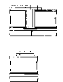
图19是具有贯通电极的BGA型半导体装置的贯通电极部的剖面图。在由硅(Si)等构成的半导体衬底10的表面介由层间绝缘膜12形成有焊盘电极11。在半导体衬底10的表面介由树脂层14粘接例如玻璃衬底等支承体13。且形成有贯通半导体衬底10并到达焊盘电极11的通孔16。在该通孔16的侧壁及半导体衬底10的背面形成有由氧化硅膜(SiO2膜)或氮化硅膜(SiN膜)等构成的绝缘膜17。19 is a cross-sectional view of a through-electrode portion of a BGA type semiconductor device having a through-electrode. A
在通孔16之中形成有与焊盘电极11连接的势垒籽晶层20及贯通电极21。在半导体衬底10的表面延伸设置有与贯通电极21相连的配线层22。覆盖半导体衬底10背面的贯通电极21、配线层22及绝缘膜17形成有由抗焊料剂构成的保护层23。在配线层22上的保护层23形成开口部,通过该开口部形成有与配线层22连接的球状导电端子24。A
专利文献1:特开2003-309221号公报Patent Document 1: JP-A-2003-309221
但是,在上述BGA型半导体装置中,当作为一种耐久试验进行热循环负载试验时,如图20所示,主要在半导体装置的四个角部(切割后半导体衬底10的角部)存在保护膜23剥离或保护膜23及其下层的绝缘膜17两者自半导体衬底10剥离且半导体装置的可靠性劣化的问题。其原因可考虑:在半导体装置接收热循环负载的过程中,会在保护膜23及绝缘膜17施加热应力,保护膜23及其下层的绝缘膜17不能承受该热应力而产生剥离。However, in the above-mentioned BGA type semiconductor device, when a thermal cycle load test is performed as a durability test, as shown in FIG. There is a problem that the
发明内容Contents of the invention
本发明的半导体装置包括:半导体衬底;焊盘电极,其介由第一绝缘膜形成于所述半导体衬底的表面;通孔,其贯通所述半导体衬底并到达所述焊盘电极;第二绝缘膜,其覆盖所述通孔的侧壁及半导体衬底的背面;贯通电极,其形成于所述通孔之中,且与所述焊盘电极连接;剥离防止层,其形成于所述第二绝缘膜上;保护层,其覆盖所述贯通电极、所述第二绝缘膜及所述剥离防止层。The semiconductor device of the present invention includes: a semiconductor substrate; a pad electrode formed on the surface of the semiconductor substrate through a first insulating film; a via hole penetrating the semiconductor substrate and reaching the pad electrode; A second insulating film covering side walls of the through hole and a back surface of the semiconductor substrate; a through electrode formed in the through hole and connected to the pad electrode; a peeling prevention layer formed on the On the second insulating film; a protective layer covering the through-electrode, the second insulating film, and the peeling prevention layer.
根据这种结构,利用剥离防止层的锚固效应防止其上层的保护层的剥离,位于保护层下层的第二绝缘膜也难于剥离。另外,所述剥离防止层设于所述半导体衬底的角部。由于保护膜的剥离容易在应力集中的半导体衬底的角部产生,故通过在该部分配置剥离防止层可有效地防止保护膜等的剥离。According to this structure, the peeling of the protective layer above it is prevented by the anchoring effect of the peeling prevention layer, and the second insulating film positioned below the protective layer is also difficult to peel off. In addition, the peeling prevention layer is provided at a corner of the semiconductor substrate. Since peeling of the protective film tends to occur at corners of the semiconductor substrate where stress is concentrated, disposing the peeling prevention layer at this portion can effectively prevent peeling of the protective film and the like.
另外,在所述半导体衬底的背面形成有槽或孔部,所述第二绝缘膜及所述剥离防止层的一部分配置于该槽或孔部之中。根据该结构,尤其可对第二绝缘膜得到锚固效应,可进一步提高剥离防止效果。且所述保护层被分割为多个岛区域。根据该结构,缓和了施加在保护层的热应力,故有利于防止保护层的剥离。还具有防止剥离进展的效果。In addition, a groove or a hole is formed on the back surface of the semiconductor substrate, and a part of the second insulating film and the detachment preventing layer is arranged in the groove or the hole. According to this configuration, an anchor effect can be obtained particularly on the second insulating film, and the effect of preventing peeling can be further enhanced. And the protection layer is divided into a plurality of island regions. According to this structure, the thermal stress applied to the protective layer is relaxed, which is advantageous in preventing peeling of the protective layer. It also has the effect of preventing the progress of peeling.
另外,本发明的半导体装置的制造方法包括:准备介由第一绝缘膜在其表面形成有焊盘电极的半导体衬底,在与所述焊盘电极对应的位置形成贯通所述半导体衬底的通孔的工序;形成覆盖所述通孔的侧壁及所述半导体衬底的背面的第二绝缘膜的工序;同时形成在所述通孔之中与所述焊盘电极连接的贯通电极及所述半导体衬底背面上的所述第二绝缘膜上的剥离防止层的工序;形成覆盖所述贯通电极、所述第二绝缘膜及所述剥离防止层的保护层的工序。In addition, the method of manufacturing a semiconductor device according to the present invention includes: preparing a semiconductor substrate having a pad electrode formed on its surface through a first insulating film, and forming a hole penetrating through the semiconductor substrate at a position corresponding to the pad electrode. the step of forming a through hole; the step of forming a second insulating film covering the side wall of the through hole and the back surface of the semiconductor substrate; simultaneously forming a through electrode connected to the pad electrode in the through hole and a step of forming a peeling prevention layer on the second insulating film on the back surface of the semiconductor substrate; and a step of forming a protective layer covering the through electrode, the second insulating film, and the peeling preventing layer.
根据该制造方法,不仅可得到防止保护层等剥离的效果,而且,由于同时形成贯通电极和剥离防止层,故可得到不需设置用于形成剥离防止层的特殊工序这一制造方法特有的效果。利用电解镀敷法同时形成贯通电极和剥离防止层有利于缩短制造工序。According to this manufacturing method, not only the effect of preventing peeling of the protective layer, etc. can be obtained, but also the unique effect of the manufacturing method that does not require a special process for forming the peeling preventing layer can be obtained because the through electrode and the peeling preventing layer are formed at the same time. . Simultaneous formation of the penetrating electrodes and the peeling prevention layer by the electrolytic plating method is advantageous in shortening the manufacturing process.
根据本发明的半导体装置,在具有贯通电极的半导体装置中,可防止保护膜及绝缘膜的剥离,故可提高半导体装置的可靠性。According to the semiconductor device of the present invention, in the semiconductor device having the penetrating electrode, peeling of the protective film and the insulating film can be prevented, so that the reliability of the semiconductor device can be improved.
附图说明Description of drawings
图1是本发明实施例1的半导体装置的平面图;1 is a plan view of a semiconductor device according to
图2是本发明实施例1的半导体装置的角部放大平面图;2 is an enlarged plan view of a corner of the semiconductor device according to
图3是沿图2的X-X线的剖面图;Fig. 3 is a sectional view along the line X-X of Fig. 2;
图4(a)、(b)是说明本发明实施例1的半导体装置的制造方法的剖面图;4(a), (b) are cross-sectional views illustrating a method of manufacturing a semiconductor device according to
图5(a)、(b)是说明本发明实施例1的半导体装置的制造方法的剖面图;5(a), (b) are cross-sectional views illustrating a method of manufacturing a semiconductor device according to
图6(a)、(b)是说明本发明实施例1的半导体装置的制造方法的剖面图;6(a), (b) are cross-sectional views illustrating a method of manufacturing a semiconductor device according to
图7(a)、(b)是说明本发明实施例1的半导体装置的制造方法的剖面图;7(a), (b) are cross-sectional views illustrating a method of manufacturing a semiconductor device according to
图8(a)、(b)是说明本发明实施例1的半导体装置的制造方法的剖面图;8(a), (b) are cross-sectional views illustrating a method of manufacturing a semiconductor device according to
图9(a)、(b)是说明本发明实施例1的半导体装置的制造方法的剖面图;9(a), (b) are cross-sectional views illustrating a method of manufacturing a semiconductor device according to
图10(a)、(b)是说明本发明实施例1的半导体装置的制造方法的剖面图;10(a), (b) are cross-sectional views illustrating a method of manufacturing a semiconductor device according to
图11(a)、(b)是说明本发明实施例1的半导体装置的制造方法的剖面图;11(a), (b) are cross-sectional views illustrating a method of manufacturing a semiconductor device according to
图12是本发明实施例2的半导体装置的角部放大平面图;12 is an enlarged plan view of a corner of a semiconductor device according to Embodiment 2 of the present invention;
图13是沿图12的X-X线的剖面图;Fig. 13 is a sectional view along the X-X line of Fig. 12;
图14(a)、(b)是说明本发明实施例2的半导体装置的制造方法的剖面图;14(a), (b) are cross-sectional views illustrating a method of manufacturing a semiconductor device according to Embodiment 2 of the present invention;
图15(a)、(b)是说明本发明实施例2的半导体装置的制造方法的剖面图;15(a), (b) are cross-sectional views illustrating a method of manufacturing a semiconductor device according to Embodiment 2 of the present invention;
图16(a)、(b)是说明本发明实施例2的半导体装置的制造方法的剖面图;16(a), (b) are cross-sectional views illustrating a method of manufacturing a semiconductor device according to Embodiment 2 of the present invention;
图17是本发明实施例2的半导体装置的角部放大平面图;17 is an enlarged plan view of a corner of a semiconductor device according to Embodiment 2 of the present invention;
图18(a)、(b)是沿图17的X-X线的剖面图;Fig. 18 (a), (b) is the sectional view along the X-X line of Fig. 17;
图19是现有例的半导体装置的贯通电极部的剖面图;19 is a cross-sectional view of a penetrating electrode portion of a conventional semiconductor device;
图20是现有例的半导体装置的角部的剖面图。20 is a cross-sectional view of a corner of a conventional semiconductor device.
具体实施方式Detailed ways
下面,参照附图说明本发明实施例1。图1是从背面看半导体装置100的平面,图2是其角部的放大平面图,图3是沿图1、图2的X-X线的剖面图。图11(a)是沿图1Y-Y线的剖面图。Next,
如图1所示,在该半导体装置100的背面矩阵状配置有多个球状导电端子24,各个导电端子24通过贯通电极21、配线层22与半导体装置表面的焊盘电极11连接。图11(a)的剖面图与现有例中说明的图19基本相同。As shown in FIG. 1 , a plurality of spherical
在本实施例中,在半导体装置100的四个角部形成有用于防止绝缘膜17、保护膜23的剥离的剥离防止层30。通过将剥离防止层30配置于角部以外的半导体装置10的空隙例如球状导电端子24之间,可提高剥离防止效果。剥离防止层30的图案形状是任意的,例如可以是图2的十字状形状,也可以是矩形。In the present embodiment, peeling prevention layers 30 for preventing peeling of the insulating
其剖面结构如图3所示,在形成于半导体衬底10的背面的绝缘膜17上形成有剥离防止层30,覆盖该绝缘膜17及剥离防止层30形成有由抗焊料剂等构成的保护层30。在剥离防止层30利用电解镀敷法形成时,具有由势垒籽晶层20和上层的铜层25构成的层积结构,但也可以由与保护层30附着性好的单一金属层构成。通常,与氧化膜等绝缘膜比较,铜与由抗焊料剂等构成的保护层23的附着性更好,锚固效应大,故最好剥离防止层30至少包括铜层。Its cross-sectional structure is shown in FIG. 3 , on the insulating
下面参照图4~图11说明设有上述剥离防止层30的半导体装置100的制造方法。这里,图4~图11中上侧的图(a)对应图1的沿Y-Y线的剖面图,下侧的图(b)对应图1的沿X-X线的剖面图。Next, a method of manufacturing the
首先,如图4所示,准备了表面形成有未图示的电子器件的半导体衬底10。未图示的电子器件例如为CCD(Charge Coupled Device)及红外线传感器等受光元件或作为发光元件的器件。或者未图示的电子器件也可以是上述受光元件及发光元件以外的电子器件。First, as shown in FIG. 4 , a
另外,在半导体衬底10的表面形成有与未图示的电子器件连接的外部连接用电极即焊盘电极11。焊盘电极11介由第一绝缘膜即层间绝缘膜12形成于半导体衬底10的表面。In addition, on the surface of the
这里,半导体衬底10例如由硅(Si)构成,理想的是具有约20~200μm的膜厚。另外,焊盘电极11例如由铝(Al)构成,理想的是具有约1μm的膜厚。另外,层间绝缘膜12例如由氧化膜构成,理想的是具有0.8μm的膜厚。Here, the
另外,在半导体衬底10的表面根据需要可形成支承体13。该支承体13介由树脂层14形成于半导体衬底10的表面。这里,在未图示的电子器件是受光元件或发光元件时,支承体13由例如玻璃等具有透明或半透明性状的材料形成。在未图示的电子器件不是受光元件或发光元件时,支承体13也可以由不具有透明或半透明性状的材料形成。另外,支承体13可以是带状体。该支承体13可以在之后工序除去。或者支承体13也可以不被除去而留下来。In addition, the
然后,如图5所示,在半导体衬底10的背面上选择性地形成第一抗蚀层15a。即第一抗蚀层15a在半导体衬底10的背面中与焊盘电极11对应的位置具有开口部。然后,以该第一抗蚀层15a为掩膜,理想的是利用干式蚀刻法蚀刻半导体衬底10。作为干式蚀刻的蚀刻气体可采用公知的CHF3等。Then, as shown in FIG. 5 , a first resist
通过该蚀刻,从背面至表面贯通对应焊盘电极11的位置的半导体衬底10,形成通孔16。在通孔16的底部,露出层间绝缘膜12,其下方连接焊盘电极11。然后,以第一抗蚀层15a为掩膜,利用干式蚀刻或湿式蚀刻,蚀刻在通孔16底部露出的层间绝缘膜12,使其形成薄膜或被完全除去。或者,层间绝缘膜12的蚀刻工序也可以不在该工序进行而和后述的其他蚀刻工序同时进行。Through this etching, a via
然后,在除去第一抗蚀层15a后,如图6所示,包括通孔16内部,在半导体衬底10的整个背面形成第二绝缘膜即绝缘膜17。这里,绝缘膜17例如由氧化硅膜(SiO2膜)或氮化硅膜(SiN膜)构成,利用例如等离子CVD法形成。Then, after removing the first resist
然后,如图7所示,在绝缘膜17上形成第二抗蚀层18。然后,如图8所示,以第二抗蚀层18为掩膜,蚀刻除去通孔16底部的绝缘膜17(在残留层间绝缘膜12时将其一并除去)。该蚀刻最好为例如反应性离子蚀刻,但也可以是其他蚀刻。通过上述蚀刻,可使形成于通孔16侧壁的绝缘膜17留下而除去该底部的绝缘膜17,露出焊盘电极11。上述蚀刻后除去第二抗蚀层18。Then, as shown in FIG. 7 , a second resist
然后,如图9所示,在包括通孔16的半导体衬底10的背面的绝缘膜17上形成势垒籽晶层20。势垒籽晶层20具有由未图示的势垒金属层和籽晶层构成的层积结构。这里,上述势垒金属层例如由钨化钛(TiW)层、氮化钛(TiN)层或者氮化钽(TaN)层等金属构成。上述籽晶层构成用于镀敷形成后述配线层22的电极,例如由铜(Cu)等金属构成。势垒籽晶层20例如由溅射法、CVD法、无电解镀敷法或其他成膜方法形成。另外,在通孔16的侧壁的绝缘膜17由氮化硅膜(SiN膜)形成时,该氮化硅膜(SiN膜)形成铜扩散的势垒,故势垒籽晶层20也可以具有仅由铜(Cu)构成的籽晶层形成的单层结构。Then, as shown in FIG. 9 ,
然后,在包括通孔16内部在内的势垒籽晶层20上利用例如电解镀敷法形成由铜(Cu)构成的贯通电极21及与该贯通电极21连接的配线层22。镀敷膜厚被调节为将贯通电极21完全或不完全埋入通孔16内的厚度。这里,贯通电极21及配线层22介由势垒籽晶层20与在通孔16底部露出的焊盘电极11电连接。利用该电解镀敷,在半导体装置的角部,如图9(b)所示,在势垒籽晶层20上形成与配线层22连接的铜层25。Then, through-
然后,如图10所示,在半导体衬底10的背面的配线层22上及铜层25上,选择性形成用于将配线层22及铜层25构图为规定图案的第三抗蚀层15b。第三抗蚀层15b形成于对应规定图案残留的配线层22及铜层25的区域上。残留的配线层22的区域至少包括通孔16的形成区域、剥离防止层30的形成区域。Then, as shown in FIG. 10, on the
然后,以第三抗蚀层15b为掩膜,蚀刻除去不需要的配线层22、铜层25及势垒籽晶层20。通过该蚀刻配线层22被构图为规定的图案。而在图10(b)中,利用该蚀刻形成由铜层25及势垒籽晶层20构成的剥离防止层30。Then, using the third resist
然后,如图11所示,在除去第三抗蚀层15b后,在半导体衬底10的背面上,覆盖它形成例如由抗焊料剂等抗蚀剂材料等构成的保护层23。在保护层23中对应配线层22的位置设置开口部。然后,在于该开口部露出的配线层22上利用网印法形成例如由焊锡等金属构成的球状导电端子24。Then, as shown in FIG. 11, after the third resist
利用以上工序完成在角部具有剥离防止层30且由半导体芯片10及层积于其上的各层构成的半导体装置100。以上工序利用晶片工序进行,故可在一张晶片上同时形成多个半导体装置100。通过沿多个半导体装置100的边界即切割线进行切割,切断分离为图1所示的各个半导体装置100。Through the above steps, the
下面参照附图说明本发明的实施例2。图12是半导体装置100的角部的放大平面图,图13是沿图12的X-X线的剖面图。本实施例与实施例1的不同点是在半导体衬底100的背面形成槽或孔部28,绝缘膜17及剥离防止层30的一部分配置在该槽或孔部28中。由此,特别是绝缘膜17和半导体衬底10利用槽或孔部28的锚固效应而牢固附着,故剥离防止效果更高。Embodiment 2 of the present invention will be described below with reference to the drawings. FIG. 12 is an enlarged plan view of a corner portion of the
参照图14~图16说明本实施例的半导体装置的制造方法。图14~图16中上侧的图(a)对应图1的沿Y-Y线的剖面图,下侧的图(b)对应图12的沿X-X线的剖面图。A method of manufacturing the semiconductor device of this embodiment will be described with reference to FIGS. 14 to 16 . 14 to 16, the upper diagram (a) corresponds to the sectional view along the Y-Y line of FIG. 1 , and the lower diagram (b) corresponds to the sectional view along the X-X line of FIG. 12 .
首先,如图14所示,与实施例1同样,准备了形成有未图示的电子器件的半导体衬底10。在半导体衬底10的表面形成与未图示的电子器件连接的外部连接用电极即焊盘电极11。焊盘电极11介由第一绝缘膜即层间绝缘膜12形成于半导体衬底10的表面。在半导体衬底10的表面根据需要可形成支承体13。First, as shown in FIG. 14 , as in Example 1, a
然后,如图15所示,在半导体衬底10的背面上选择性形成第一抗蚀层15a。即第一抗蚀层15a具有与对应焊盘电极11的区域对应的第一开口部,和与形成剥离防止层30的区域对应的第二开口部。这里,第二开口部设定得小于第一开口部。例如,若第一开口部为大于或等于数十μm,则第二开口部为约5μm。Then, as shown in FIG. 15 , a first resist
然后,以该第一抗蚀层15a为掩膜,利用干式蚀刻法蚀刻半导体衬底10。作为蚀刻气体可采用公知的CHF3等。通过该蚀刻,形成贯通对应焊盘电极11的区域的半导体衬底10的通孔16及不贯通半导体衬底10的槽或孔部28。这是由于第二开口部的开口直径较小,蚀刻气体不易从此处进入其中,因此,在通孔16完全形成的时刻,该部分还未到贯通半导体衬底10的程度。若半导体衬底10的厚度为130μm,则槽或孔部28的深度为50μm左右。然后,通过进行与实施例1同样的工序,如图16所示,得到具有局部埋入槽或孔部28的剥离防止层30的半导体装置。Then, using the first resist
下面参照附图说明本发明的实施例3。图17是半导体装置100的角部的放大平面图,图18(a)是沿图17的X-X线的剖面图。本实施例与实施例1的不同点是保护层23隔着多个缝隙SL被分割为多个岛区域23A。尤其是在半导体装置100的角部形成这种岛区域23A是有效的。但也可以在半导体装置100的整个面上形成岛区域23A。这样通过将由抗焊料剂等构成的保护层23分割为多个岛区域23A,可分散热应力,防止保护膜23及绝缘膜17的剥离。将保护层23分割为多个岛区域23A的工序可以与在保护层23上开设用于形成球状导电端子24的开口部的工序同时进行。Embodiment 3 of the present invention will be described below with reference to the drawings. FIG. 17 is an enlarged plan view of a corner portion of the
本实施例的特征结构也可以应用于实施例2。即如图18(b)所示,在半导体衬底100的背面形成槽或孔部28,将绝缘膜17及剥离防止层30的一部分配置在该槽或孔部28之中。然后,在半导体装置100的角部或半导体装置100的整个面上形成岛区域23A。The characteristic structure of this embodiment can also be applied to Embodiment 2. That is, as shown in FIG. 18( b ), grooves or holes 28 are formed on the back surface of the
另外,也可以不形成剥离防止层30而在保护层23形成缝隙。In addition, it is also possible to form a slit in the
Claims (16)
Applications Claiming Priority (2)
| Application Number | Priority Date | Filing Date | Title |
|---|---|---|---|
| JP2004284794A JP4966487B2 (en) | 2004-09-29 | 2004-09-29 | Semiconductor device and manufacturing method thereof |
| JP284794/04 | 2004-09-29 |
Publications (2)
| Publication Number | Publication Date |
|---|---|
| CN1755916A true CN1755916A (en) | 2006-04-05 |
| CN100530609C CN100530609C (en) | 2009-08-19 |
Family
ID=36124738
Family Applications (1)
| Application Number | Title | Priority Date | Filing Date |
|---|---|---|---|
| CNB2005101068638A Expired - Fee Related CN100530609C (en) | 2004-09-29 | 2005-09-26 | Semiconductor device and manufacturing method of the same |
Country Status (5)
| Country | Link |
|---|---|
| US (2) | US7382037B2 (en) |
| JP (1) | JP4966487B2 (en) |
| KR (1) | KR100648122B1 (en) |
| CN (1) | CN100530609C (en) |
| TW (1) | TWI305020B (en) |
Cited By (7)
| Publication number | Priority date | Publication date | Assignee | Title |
|---|---|---|---|---|
| CN102157483A (en) * | 2010-01-20 | 2011-08-17 | 精材科技股份有限公司 | Chip package and method for forming the same |
| CN102224579A (en) * | 2008-11-25 | 2011-10-19 | 松下电器产业株式会社 | Semiconductor device and electronic device |
| CN102473640A (en) * | 2010-05-31 | 2012-05-23 | 松下电器产业株式会社 | Semiconductor device and method for manufacturing the same |
| CN103367139A (en) * | 2013-07-11 | 2013-10-23 | 华进半导体封装先导技术研发中心有限公司 | TSV hole bottom medium layer etching method |
| CN104617036A (en) * | 2015-01-14 | 2015-05-13 | 华天科技(昆山)电子有限公司 | Manufacturing method for interconnected through holes in wafer level chip size packaging |
| CN105684140A (en) * | 2013-06-29 | 2016-06-15 | 英特尔公司 | Interconnect structure comprising fine pitch backside metal redistribution lines combined with vias |
| WO2024124532A1 (en) * | 2022-12-16 | 2024-06-20 | 京东方科技集团股份有限公司 | Functional substrate and preparation method therefor |
Families Citing this family (31)
| Publication number | Priority date | Publication date | Assignee | Title |
|---|---|---|---|---|
| JP4675146B2 (en) * | 2005-05-10 | 2011-04-20 | パナソニック株式会社 | Semiconductor device |
| US8154131B2 (en) | 2005-06-14 | 2012-04-10 | Cufer Asset Ltd. L.L.C. | Profiled contact |
| US7560813B2 (en) | 2005-06-14 | 2009-07-14 | John Trezza | Chip-based thermo-stack |
| US8456015B2 (en) | 2005-06-14 | 2013-06-04 | Cufer Asset Ltd. L.L.C. | Triaxial through-chip connection |
| US7838997B2 (en) | 2005-06-14 | 2010-11-23 | John Trezza | Remote chip attachment |
| US7687400B2 (en) | 2005-06-14 | 2010-03-30 | John Trezza | Side stacking apparatus and method |
| US7781886B2 (en) | 2005-06-14 | 2010-08-24 | John Trezza | Electronic chip contact structure |
| US7767493B2 (en) | 2005-06-14 | 2010-08-03 | John Trezza | Post & penetration interconnection |
| US7786592B2 (en) | 2005-06-14 | 2010-08-31 | John Trezza | Chip capacitive coupling |
| US7851348B2 (en) | 2005-06-14 | 2010-12-14 | Abhay Misra | Routingless chip architecture |
| US8786092B2 (en) | 2005-06-17 | 2014-07-22 | Rohm Co., Ltd. | Semiconductor integrated circuit device |
| JP2007311771A (en) * | 2006-04-21 | 2007-11-29 | Sanyo Electric Co Ltd | Semiconductor device and manufacturing method thereof |
| US7687397B2 (en) * | 2006-06-06 | 2010-03-30 | John Trezza | Front-end processed wafer having through-chip connections |
| JP4302720B2 (en) * | 2006-06-28 | 2009-07-29 | 株式会社沖データ | Semiconductor device, LED head, and image forming apparatus |
| US7670874B2 (en) | 2007-02-16 | 2010-03-02 | John Trezza | Plated pillar package formation |
| USD597428S1 (en) * | 2007-04-02 | 2009-08-04 | Asahi Kasei Emd Corporation | Infrared ray sensor |
| JP4659875B2 (en) * | 2008-11-25 | 2011-03-30 | パナソニック株式会社 | Semiconductor device |
| JP2010129952A (en) * | 2008-12-01 | 2010-06-10 | Nippon Telegr & Teleph Corp <Ntt> | Method of manufacturing through electrode wiring |
| KR101571353B1 (en) | 2009-02-16 | 2015-11-24 | 삼성전자 주식회사 | Image sensor and method of fabricating the same |
| US8426938B2 (en) * | 2009-02-16 | 2013-04-23 | Samsung Electronics Co., Ltd. | Image sensor and method of fabricating the same |
| US8264067B2 (en) * | 2009-10-09 | 2012-09-11 | Taiwan Semiconductor Manufacturing Company, Ltd. | Through silicon via (TSV) wire bond architecture |
| US8399987B2 (en) * | 2009-12-04 | 2013-03-19 | Samsung Electronics Co., Ltd. | Microelectronic devices including conductive vias, conductive caps and variable thickness insulating layers |
| US20110204517A1 (en) * | 2010-02-23 | 2011-08-25 | Qualcomm Incorporated | Semiconductor Device with Vias Having More Than One Material |
| US8896136B2 (en) * | 2010-06-30 | 2014-11-25 | Taiwan Semiconductor Manufacturing Company, Ltd. | Alignment mark and method of formation |
| JP5700502B2 (en) * | 2010-07-28 | 2015-04-15 | 住友電工デバイス・イノベーション株式会社 | Semiconductor device and manufacturing method |
| EP2655700A1 (en) * | 2010-12-23 | 2013-10-30 | Centre de Recherche Public - Gabriel Lippmann | An ecpr master electrode and a method for providing such ecpr master electrode |
| JP5360134B2 (en) * | 2011-06-01 | 2013-12-04 | 三菱電機株式会社 | Semiconductor device and manufacturing method thereof |
| US8546900B2 (en) | 2011-06-09 | 2013-10-01 | Optiz, Inc. | 3D integration microelectronic assembly for integrated circuit devices |
| US20140151095A1 (en) * | 2012-12-05 | 2014-06-05 | Samsung Electro-Mechanics Co., Ltd. | Printed circuit board and method for manufacturing the same |
| JP6443362B2 (en) * | 2016-03-03 | 2018-12-26 | 株式会社デンソー | Semiconductor device |
| KR102619817B1 (en) * | 2022-05-19 | 2024-01-02 | 세메스 주식회사 | Method of forming semiconductor device and substrate processing system for forming semiconductor device |
Family Cites Families (29)
| Publication number | Priority date | Publication date | Assignee | Title |
|---|---|---|---|---|
| JPS59163841A (en) * | 1983-03-08 | 1984-09-14 | Toshiba Corp | Resin sealed semiconductor device |
| JPS61269333A (en) * | 1985-05-24 | 1986-11-28 | Hitachi Ltd | Semiconductor device |
| US5399898A (en) * | 1992-07-17 | 1995-03-21 | Lsi Logic Corporation | Multi-chip semiconductor arrangements using flip chip dies |
| JP2541028Y2 (en) * | 1989-11-17 | 1997-07-09 | ソニー株式会社 | Semiconductor device |
| US5229647A (en) * | 1991-03-27 | 1993-07-20 | Micron Technology, Inc. | High density data storage using stacked wafers |
| US5561082A (en) * | 1992-07-31 | 1996-10-01 | Kabushiki Kaisha Toshiba | Method for forming an electrode and/or wiring layer by reducing copper oxide or silver oxide |
| US5432999A (en) * | 1992-08-20 | 1995-07-18 | Capps; David F. | Integrated circuit lamination process |
| US5424245A (en) * | 1994-01-04 | 1995-06-13 | Motorola, Inc. | Method of forming vias through two-sided substrate |
| US5814889A (en) * | 1995-06-05 | 1998-09-29 | Harris Corporation | Intergrated circuit with coaxial isolation and method |
| US5973396A (en) * | 1996-02-16 | 1999-10-26 | Micron Technology, Inc. | Surface mount IC using silicon vias in an area array format or same size as die array |
| US6809421B1 (en) * | 1996-12-02 | 2004-10-26 | Kabushiki Kaisha Toshiba | Multichip semiconductor device, chip therefor and method of formation thereof |
| US5915167A (en) * | 1997-04-04 | 1999-06-22 | Elm Technology Corporation | Three dimensional structure memory |
| JPH1167755A (en) * | 1997-08-21 | 1999-03-09 | Seiko Epson Corp | Semiconductor structure |
| DE69737262T2 (en) * | 1997-11-26 | 2007-11-08 | Stmicroelectronics S.R.L., Agrate Brianza | A method of manufacturing a front-to-back via in micro-integrated circuits |
| US6833613B1 (en) * | 1997-12-18 | 2004-12-21 | Micron Technology, Inc. | Stacked semiconductor package having laser machined contacts |
| DE19853703A1 (en) * | 1998-11-20 | 2000-05-25 | Giesecke & Devrient Gmbh | Chip production, especially for a chip card, comprises applying metallization onto a thinned finished chip wafer, bonded to a handling wafer, for connection by vias to the chip metallization and/or circuit structure |
| JP2001168093A (en) * | 1999-12-09 | 2001-06-22 | Sharp Corp | Semiconductor device |
| US6710446B2 (en) * | 1999-12-30 | 2004-03-23 | Renesas Technology Corporation | Semiconductor device comprising stress relaxation layers and method for manufacturing the same |
| JP3879816B2 (en) * | 2000-06-02 | 2007-02-14 | セイコーエプソン株式会社 | SEMICONDUCTOR DEVICE AND ITS MANUFACTURING METHOD, LAMINATED SEMICONDUCTOR DEVICE, CIRCUIT BOARD AND ELECTRONIC DEVICE |
| JP3530149B2 (en) * | 2001-05-21 | 2004-05-24 | 新光電気工業株式会社 | Wiring board manufacturing method and semiconductor device |
| US6848177B2 (en) * | 2002-03-28 | 2005-02-01 | Intel Corporation | Integrated circuit die and an electronic assembly having a three-dimensional interconnection scheme |
| JP4212293B2 (en) * | 2002-04-15 | 2009-01-21 | 三洋電機株式会社 | Manufacturing method of semiconductor device |
| TWI229435B (en) * | 2002-06-18 | 2005-03-11 | Sanyo Electric Co | Manufacture of semiconductor device |
| TWI227050B (en) * | 2002-10-11 | 2005-01-21 | Sanyo Electric Co | Semiconductor device and method for manufacturing the same |
| JP4397583B2 (en) * | 2002-12-24 | 2010-01-13 | 株式会社フジクラ | Semiconductor device |
| US6833323B2 (en) * | 2003-01-29 | 2004-12-21 | Taiwan Semiconductor Manufacturing Co., Ltd | Method for forming patterned features at a semiconductor wafer periphery to prevent metal peeling |
| JP3800335B2 (en) * | 2003-04-16 | 2006-07-26 | セイコーエプソン株式会社 | Optical device, optical module, semiconductor device, and electronic apparatus |
| JP4248928B2 (en) * | 2003-05-13 | 2009-04-02 | ローム株式会社 | Semiconductor chip manufacturing method, semiconductor device manufacturing method, semiconductor chip, and semiconductor device |
| JP4467318B2 (en) * | 2004-01-28 | 2010-05-26 | Necエレクトロニクス株式会社 | Semiconductor device, chip alignment method for multi-chip semiconductor device, and method for manufacturing chip for multi-chip semiconductor device |
-
2004
- 2004-09-29 JP JP2004284794A patent/JP4966487B2/en not_active Expired - Lifetime
-
2005
- 2005-08-31 TW TW094129820A patent/TWI305020B/en not_active IP Right Cessation
- 2005-09-23 KR KR1020050088565A patent/KR100648122B1/en active IP Right Grant
- 2005-09-26 CN CNB2005101068638A patent/CN100530609C/en not_active Expired - Fee Related
- 2005-09-28 US US11/236,881 patent/US7382037B2/en active Active
-
2008
- 2008-04-25 US US12/109,800 patent/US7906430B2/en active Active
Cited By (10)
| Publication number | Priority date | Publication date | Assignee | Title |
|---|---|---|---|---|
| CN102224579A (en) * | 2008-11-25 | 2011-10-19 | 松下电器产业株式会社 | Semiconductor device and electronic device |
| CN102224579B (en) * | 2008-11-25 | 2013-12-04 | 松下电器产业株式会社 | Semiconductor device and electronic device |
| CN102157483A (en) * | 2010-01-20 | 2011-08-17 | 精材科技股份有限公司 | Chip package and method for forming the same |
| CN102157483B (en) * | 2010-01-20 | 2015-11-25 | 精材科技股份有限公司 | Chip package and method of forming the same |
| CN102473640A (en) * | 2010-05-31 | 2012-05-23 | 松下电器产业株式会社 | Semiconductor device and method for manufacturing the same |
| CN105684140A (en) * | 2013-06-29 | 2016-06-15 | 英特尔公司 | Interconnect structure comprising fine pitch backside metal redistribution lines combined with vias |
| CN105684140B (en) * | 2013-06-29 | 2019-11-05 | 英特尔公司 | Interconnection structure including the fine spacing back metal redistribution lines in conjunction with via hole |
| CN103367139A (en) * | 2013-07-11 | 2013-10-23 | 华进半导体封装先导技术研发中心有限公司 | TSV hole bottom medium layer etching method |
| CN104617036A (en) * | 2015-01-14 | 2015-05-13 | 华天科技(昆山)电子有限公司 | Manufacturing method for interconnected through holes in wafer level chip size packaging |
| WO2024124532A1 (en) * | 2022-12-16 | 2024-06-20 | 京东方科技集团股份有限公司 | Functional substrate and preparation method therefor |
Also Published As
| Publication number | Publication date |
|---|---|
| KR100648122B1 (en) | 2006-11-24 |
| JP2006100558A (en) | 2006-04-13 |
| US20060071342A1 (en) | 2006-04-06 |
| US20080254618A1 (en) | 2008-10-16 |
| TWI305020B (en) | 2009-01-01 |
| US7906430B2 (en) | 2011-03-15 |
| TW200629442A (en) | 2006-08-16 |
| JP4966487B2 (en) | 2012-07-04 |
| CN100530609C (en) | 2009-08-19 |
| KR20060051564A (en) | 2006-05-19 |
| US7382037B2 (en) | 2008-06-03 |
Similar Documents
| Publication | Publication Date | Title |
|---|---|---|
| CN1755916A (en) | Semiconductor device and manufacturing method thereof | |
| CN101937894B (en) | Semiconductor device including through-electrode and method of manufacturing the same | |
| KR100721492B1 (en) | Semiconductor device and manufacturing method thereof | |
| CN101373720B (en) | Method of manufacturing semiconductor device | |
| JP4307284B2 (en) | Manufacturing method of semiconductor device | |
| JP4850392B2 (en) | Manufacturing method of semiconductor device | |
| CN1574403A (en) | Optical semiconductor device and method of manufacturing same | |
| CN1658385A (en) | Semiconductor device and manufacturing method thereof | |
| CN1523665A (en) | Semiconductor device and manufacturing method thereof | |
| CN1825590A (en) | Semiconductor device and manufacturing method thereof | |
| JP4456027B2 (en) | Method for manufacturing through conductor | |
| CN101083241A (en) | Semiconductor device and its manufacturing method | |
| US7557017B2 (en) | Method of manufacturing semiconductor device with two-step etching of layer | |
| CN1551344A (en) | Semiconductor device, stacked semiconductor device, and their manufacturing method | |
| CN102224579B (en) | Semiconductor device and electronic device | |
| JP4544902B2 (en) | Semiconductor device and manufacturing method thereof | |
| CN1716619A (en) | SOI substrate and its manufacturing method | |
| CN1790686A (en) | Semiconductor device packaged into chip size and manufacturing method thereof | |
| CN1231955C (en) | Bonding pad structure and manufacturing method thereof | |
| CN1630071A (en) | Semiconductor device, manufacturing method thereof, circuit substrate, and electronic device | |
| JP4845986B2 (en) | Semiconductor device | |
| CN101567344A (en) | Semiconductor chip packaging structure capable of achieving front-side electric conduction and manufacturing method thereof |
Legal Events
| Date | Code | Title | Description |
|---|---|---|---|
| C06 | Publication | ||
| PB01 | Publication | ||
| C10 | Entry into substantive examination | ||
| SE01 | Entry into force of request for substantive examination | ||
| C14 | Grant of patent or utility model | ||
| GR01 | Patent grant | ||
| CF01 | Termination of patent right due to non-payment of annual fee |
Granted publication date: 20090819 Termination date: 20200926 |
|
| CF01 | Termination of patent right due to non-payment of annual fee |