CN1734671B - Phase change memory and method of programming phase change memory using continuous reset control - Google Patents
Phase change memory and method of programming phase change memory using continuous reset control Download PDFInfo
- Publication number
- CN1734671B CN1734671B CN200510077929.5A CN200510077929A CN1734671B CN 1734671 B CN1734671 B CN 1734671B CN 200510077929 A CN200510077929 A CN 200510077929A CN 1734671 B CN1734671 B CN 1734671B
- Authority
- CN
- China
- Prior art keywords
- phase change
- change memory
- reset
- phase
- pulse
- Prior art date
- Legal status (The legal status is an assumption and is not a legal conclusion. Google has not performed a legal analysis and makes no representation as to the accuracy of the status listed.)
- Expired - Fee Related
Links
Images


Classifications
-
- G—PHYSICS
- G11—INFORMATION STORAGE
- G11C—STATIC STORES
- G11C13/00—Digital stores characterised by the use of storage elements not covered by groups G11C11/00, G11C23/00, or G11C25/00
- G11C13/0002—Digital stores characterised by the use of storage elements not covered by groups G11C11/00, G11C23/00, or G11C25/00 using resistive RAM [RRAM] elements
- G11C13/0021—Auxiliary circuits
- G11C13/0069—Writing or programming circuits or methods
-
- G—PHYSICS
- G11—INFORMATION STORAGE
- G11C—STATIC STORES
- G11C13/00—Digital stores characterised by the use of storage elements not covered by groups G11C11/00, G11C23/00, or G11C25/00
- G11C13/0002—Digital stores characterised by the use of storage elements not covered by groups G11C11/00, G11C23/00, or G11C25/00 using resistive RAM [RRAM] elements
- G11C13/0004—Digital stores characterised by the use of storage elements not covered by groups G11C11/00, G11C23/00, or G11C25/00 using resistive RAM [RRAM] elements comprising amorphous/crystalline phase transition cells
-
- G—PHYSICS
- G11—INFORMATION STORAGE
- G11C—STATIC STORES
- G11C5/00—Details of stores covered by group G11C11/00
- G11C5/06—Arrangements for interconnecting storage elements electrically, e.g. by wiring
- G11C5/063—Voltage and signal distribution in integrated semi-conductor memory access lines, e.g. word-line, bit-line, cross-over resistance, propagation delay
-
- G—PHYSICS
- G11—INFORMATION STORAGE
- G11C—STATIC STORES
- G11C7/00—Arrangements for writing information into, or reading information out from, a digital store
- G11C7/10—Input/output [I/O] data interface arrangements, e.g. I/O data control circuits, I/O data buffers
- G11C7/1078—Data input circuits, e.g. write amplifiers, data input buffers, data input registers, data input level conversion circuits
- G11C7/1096—Write circuits, e.g. I/O line write drivers
-
- G—PHYSICS
- G11—INFORMATION STORAGE
- G11C—STATIC STORES
- G11C13/00—Digital stores characterised by the use of storage elements not covered by groups G11C11/00, G11C23/00, or G11C25/00
- G11C13/0002—Digital stores characterised by the use of storage elements not covered by groups G11C11/00, G11C23/00, or G11C25/00 using resistive RAM [RRAM] elements
- G11C13/0021—Auxiliary circuits
- G11C13/0069—Writing or programming circuits or methods
- G11C2013/0078—Write using current through the cell
-
- G—PHYSICS
- G11—INFORMATION STORAGE
- G11C—STATIC STORES
- G11C13/00—Digital stores characterised by the use of storage elements not covered by groups G11C11/00, G11C23/00, or G11C25/00
- G11C13/0002—Digital stores characterised by the use of storage elements not covered by groups G11C11/00, G11C23/00, or G11C25/00 using resistive RAM [RRAM] elements
- G11C13/0021—Auxiliary circuits
- G11C13/0069—Writing or programming circuits or methods
- G11C2013/0092—Write characterized by the shape, e.g. form, length, amplitude of the write pulse
-
- G—PHYSICS
- G11—INFORMATION STORAGE
- G11C—STATIC STORES
- G11C2213/00—Indexing scheme relating to G11C13/00 for features not covered by this group
- G11C2213/70—Resistive array aspects
- G11C2213/79—Array wherein the access device being a transistor
Landscapes
- Chemical & Material Sciences (AREA)
- Crystallography & Structural Chemistry (AREA)
- Semiconductor Memories (AREA)
- Static Random-Access Memory (AREA)
- Read Only Memory (AREA)
Abstract
本发明提供了一种相变存储器设备,其包含多个相变存储器单元和被配置为输出多个连续复位脉冲的复位脉冲生成电路。每个连续复位脉冲被输出到多条复位线中的相应一条。多个写驱动器电路连接到相应的相变存储器单元以及复位脉冲生成电路中的一条相应复位线。本发明还提供了一种使用连续复位控制信号编程相变存储器设备的方法。
The present invention provides a phase change memory device comprising a plurality of phase change memory cells and a reset pulse generating circuit configured to output a plurality of consecutive reset pulses. Each successive reset pulse is output to a corresponding one of the plurality of reset lines. A plurality of write driver circuits are connected to respective phase change memory cells and a respective reset line in the reset pulse generation circuit. The present invention also provides a method of programming a phase change memory device using a continuous reset control signal.
Description
技术领域 technical field
本发明涉及驱动器电路和用于存储器元件的驱动器电路的控制,尤其涉及用于相变存储器元件的驱动器电路和/或方法。The present invention relates to driver circuits and control of driver circuits for memory elements, in particular to driver circuits and/or methods for phase change memory elements.
背景技术 Background technique
相变存储器元件是用于使用在特定相变材料的晶相和非晶相之间的电导率或阻抗差别特征,存储信息的存储器元件。相变存储器元件形成电连接到晶体管元件等的存储器单元,其在半导体衬底上形成,用于设备的寻址和读/写操作。在该存储器元件中,使用依据存储器层区域的相变的电导率差别存储信息。A phase change memory element is a memory element for storing information using a characteristic of a difference in conductivity or impedance between a crystalline phase and an amorphous phase of a specific phase change material. A phase change memory element forms a memory cell electrically connected to a transistor element, etc., which is formed on a semiconductor substrate for addressing and read/write operations of the device. In this memory element, information is stored using a difference in conductivity according to a phase transition of a memory layer region.
图1A和图1B说明了传统的相变存储器单元10。如图1A所示,相变存储器单元10包含在顶部电极12和底部电极18之间的相变材料14。为了增加电流密度,以及因此提高相变材料14的加热效率,底部电极18可以通过与底部电极18相比具有减少的表面积的底部电极触头(BEC)16连接到相变材料14。访问晶体管20可以连接到底部电极18,并且由字线控制。1A and 1B illustrate a conventional phase
如图1A、1B和2所示,相变存储器单元10进行操作,使得流过相变材料14的电流电加热相变区域,而且相变材料14的结构可逆地转变为晶态(图1A)或者非晶态(图1B)以存储信息。在图1B中,相变材料14中的状态改变到非晶态的区域用紧邻BEC16的交叉阴影线说明。可以通过在相变区域流过相对低的电流并且测量该相变材料的阻抗来读取存储的信息。因此,图2说明了传统的相变存储器单元10,其中单元晶体管20由字线WL控制,以控制电流ICELL从位线BL流过由相变材料提供的可变阻抗C。As shown in Figures 1A, 1B and 2, the phase
在设置相变材料14的区域为晶态或者非晶态时,可以使用不同的脉冲来控制相变材料14的加热。如图3所示,高温短持续时间加热周期35用于把相变材料14复位到非晶态,而较长持续时间较低温度加热周期36用于把相变材料14置位到晶态。特别地,在短持续时间周期35中,相变材料14被加热到超过相变材料14熔点Tm的温度,然后迅速冷却,例如在几个纳秒内,以在相变材料14中创建非晶区。在较长持续时间周期36中,相变材料14被加热到高于相变材料14的晶化点Tx、且低于熔点Tm的温度,并且在那个温度保持预定时间,然后冷却以创建在相变材料14中的结晶区。因此,该温度保持在高于晶化温度Tx、且低于熔点温度Tm的置位窗口内。When the region of the phase change material 14 is set to be crystalline or amorphous, different pulses can be used to control the heating of the phase change material 14 . As shown in Figure 3, a high temperature short duration heating cycle 35 is used to reset the phase change material 14 to the amorphous state, while a longer duration lower temperature heating cycle 36 is used to set the phase change material 14 to the crystalline state. In particular, during a short duration period 35, the phase change material 14 is heated to a temperature above the melting point Tm of the phase change material 14 and then cooled rapidly, for example within a few nanoseconds, to create an amorphous state in the phase change material 14. district. During the longer duration period 36, the phase change material 14 is heated to a temperature above the crystallization point Tx of the phase change material 14, and below the melting point Tm, and held at that temperature for a predetermined time, and then cooled to create the phase change material 14. crystalline regions in variable material 14. Therefore, the temperature remains within a set window above the crystallization temperature Tx and below the melting point temperature Tm.
图4说明了用于编程相变存储器的各种电流波形。特别地,如图4所示,和置位电流相比,复位电流具有较短持续时间但是具有更大的振幅。如果多个存储器单元(例如,超过16位)被同时复位,则峰值电流可超过电源的能力,这可导致电源输出的波动。通常,在存储器单元块中被同时编程(置位和复位)的存储器单元数量已经由对复位电流的考虑所限制。Figure 4 illustrates various current waveforms for programming phase change memory. In particular, as shown in FIG. 4 , the reset current has a shorter duration but has a larger amplitude than the set current. If multiple memory cells (eg, more than 16 bits) are reset simultaneously, the peak current can exceed the capability of the power supply, which can cause fluctuations in the output of the power supply. Typically, the number of memory cells that are programmed (set and reset) simultaneously in a block of memory cells has been limited by reset current considerations.
例如,在美国专利6,545,907、6,075,719和6,487,113中描述了用于编程相变存储器的各种技术。Various techniques for programming phase change memory are described, for example, in US Patents 6,545,907, 6,075,719, and 6,487,113.
发明内容 Contents of the invention
本发明的某些实施例提供了包含多个相变存储器单元和复位脉冲生成电路的相变存储器设备,其中该复位脉冲生成电路被配置为输出多个连续复位脉冲。每个连续复位脉冲都被输出到多条复位线中的相应一条。多个写驱动器电路连接到相应的相变存储器单元以及复位脉冲生成电路中一条相应的复位线。Certain embodiments of the present invention provide a phase change memory device comprising a plurality of phase change memory cells and a reset pulse generation circuit, wherein the reset pulse generation circuit is configured to output a plurality of consecutive reset pulses. Each successive reset pulse is output to a corresponding one of the plurality of reset lines. A plurality of write driver circuits are connected to corresponding phase change memory cells and a corresponding reset line in the reset pulse generating circuit.
在进一步的实施例中,复位脉冲生成电路包含被配置为生成第一复位脉冲的第一脉冲生成电路,以及多条延迟线,其中这些延迟线串联连接到第一脉冲生成电路,以提供相继连续延迟的复位脉冲。第一脉冲生成电路可以响应于地址跃迁检测信号,生成第一复位脉冲。在其它实施例中,第一脉冲生成电路响应于数据跃迁检测信号,生成第一复位脉冲。第一脉冲生成电路可以包含与非(NAND)逻辑门,其具有第一控制信号作为第一输入,以及第一控制信号的延迟版本作为第二输入。第一脉冲生成电路可以进一步包含延迟线,其接收第一控制信号作为输入,并且向与非逻辑门的第二输入输出第一控制信号的延迟版本。此外,每一条延迟线的延迟可以大于第一复位脉冲的脉冲宽度。In a further embodiment, the reset pulse generating circuit comprises a first pulse generating circuit configured to generate a first reset pulse, and a plurality of delay lines, wherein the delay lines are connected in series to the first pulse generating circuit to provide successive delayed reset pulse. The first pulse generation circuit may generate a first reset pulse in response to the address transition detection signal. In other embodiments, the first pulse generation circuit generates the first reset pulse in response to the data transition detection signal. The first pulse generation circuit may include a NAND logic gate having a first control signal as a first input and a delayed version of the first control signal as a second input. The first pulse generating circuit may further include a delay line that receives as input the first control signal and outputs a delayed version of the first control signal to a second input of the NAND logic gate. In addition, the delay of each delay line may be greater than the pulse width of the first reset pulse.
在本发明的另外实施例中,多个写驱动器电路中的每个都连接到相变存储器单元的多条位线。这多条位线可以来自相变存储器设备的同一字,或者来自相变存储器设备的不同字。In a further embodiment of the invention, each of the plurality of write driver circuits is connected to a plurality of bit lines of the phase change memory cell. The multiple bit lines can be from the same word of the phase change memory device, or from different words of the phase change memory device.
在本发明的进一步实施例中,多个写驱动器电路中的每个都连接到相变存储器单元的单条位线。In a further embodiment of the invention, each of the plurality of write driver circuits is connected to a single bit line of the phase change memory cell.
在本发明的某些实施例中,多个连续复位脉冲中每一个的持续时间可以小于相变存储器设备的置位脉冲的持续时间。此外,相变存储器设备的置位脉冲可以具有从大约100纳秒到大约500纳秒的持续时间,而且每个连续复位脉冲可以具有从大约10到大约50纳秒的持续时间。连续复位脉冲可以彼此间隔大约10纳秒。In some embodiments of the invention, the duration of each of the plurality of consecutive reset pulses may be less than the duration of the set pulse of the phase change memory device. Additionally, a set pulse of a phase change memory device may have a duration of from about 100 nanoseconds to about 500 nanoseconds, and each successive reset pulse may have a duration of from about 10 to about 50 nanoseconds. Successive reset pulses may be spaced approximately 10 nanoseconds apart from each other.
本发明的某些实施例提供了这样的方法,其通过向共同连接到字线的相变存储器单元的子集连续地施加复位脉冲,编程包含多个相变存储器单元的存储器设备。通过向多个相变存储器单元施加第一脉冲宽度的信号复位这些相变存储器单元、以及通过向这些相变存储器单元施加第二脉冲宽度的信号进行置位,其中每个连续施加的复位脉冲的持续时间对应于第一脉冲宽度,而且连续施加的复位脉冲的持续时间总和不大于第二脉冲宽度。相变存储器单元的子集可以这样配置,使得向存储器设备的每条独立位线施加不同的复位脉冲,或者使得向该存储器设备的至少两条不同位线施加相同的复位脉冲。这两条不同的位线可以分别来自于存储器设备的不同字。Certain embodiments of the present invention provide methods of programming a memory device comprising a plurality of phase change memory cells by sequentially applying a reset pulse to a subset of the phase change memory cells commonly connected to a word line. A plurality of phase-change memory cells are reset by applying a signal of a first pulse width to the phase-change memory cells and set by applying a signal of a second pulse width to the phase-change memory cells, wherein each successively applied reset pulse The duration corresponds to the first pulse width, and the sum of the durations of consecutively applied reset pulses is not greater than the second pulse width. A subset of phase change memory cells may be configured such that a different reset pulse is applied to each individual bit line of the memory device, or such that the same reset pulse is applied to at least two different bit lines of the memory device. The two different bit lines can each be from different words of the memory device.
在本发明的进一步实施例中,由相应的写驱动器响应于对应的复位控制信号,生成连续施加的复位脉冲,而且每一写驱动器接收相同的置位控制信号。In a further embodiment of the invention, successively applied reset pulses are generated by respective write drivers in response to corresponding reset control signals, and each write driver receives the same set control signal.
在本发明的特别实施例中,连续施加的复位脉冲不重叠。相变存储器设备的置位脉冲可以具有从大约100纳秒到大约500纳秒的持续时间,而且每个连续复位脉冲可以具有从大约10到大约50纳秒的持续时间。连续复位脉冲可以彼此间隔大约10纳秒。In a particular embodiment of the invention, successively applied reset pulses do not overlap. A set pulse of a phase change memory device may have a duration of from about 100 nanoseconds to about 500 nanoseconds, and each successive reset pulse may have a duration of from about 10 to about 50 nanoseconds. Successive reset pulses may be spaced approximately 10 nanoseconds apart from each other.
本发明的某些实施例提供了一种相变存储器设备,其包含多个相变存储器单元和装置,这些装置用于向共同连接到字线的相变存储器单元的子集连续地施加复位脉冲。可以通过向多个相变存储器单元施加第一脉冲宽度的信号来复位这些相变存储器单元,以及通过向这些相变存储器单元施加第二脉冲宽度的信号来进行置位。用于连续施加复位脉冲的装置可以包含其中每个连续施加的复位脉冲的持续时间对应于第一脉冲宽度、而且连续施加的复位脉冲的持续时间总和实质上不大于第二脉冲宽度的、用于连续施加复位脉冲的装置。Certain embodiments of the present invention provide a phase change memory device comprising a plurality of phase change memory cells and means for sequentially applying a reset pulse to a subset of the phase change memory cells commonly connected to a word line . The phase change memory cells may be reset by applying a signal of a first pulse width to the phase change memory cells and set by applying a signal of a second pulse width to the phase change memory cells. The means for continuously applying a reset pulse may comprise wherein the duration of each successively applied reset pulse corresponds to the first pulse width, and the sum of the durations of the successively applied reset pulses is not substantially greater than the second pulse width, for A device that applies a reset pulse continuously.
在本发明的另外实施例中,这样配置相变存储器单元的子集,使得向存储器设备的每条独立位线施加不同的复位脉冲。在本发明的其它实施例中,这样配置相变存储器单元的子集,使得向存储器设备的至少两条不同的位线施加相同的复位脉冲。这两条不同的位线可以分别来自于存储器设备的不同字。In a further embodiment of the invention, a subset of the phase change memory cells is configured such that a different reset pulse is applied to each individual bit line of the memory device. In other embodiments of the invention, the subset of phase change memory cells is configured such that the same reset pulse is applied to at least two different bit lines of the memory device. The two different bit lines can each be from different words of the memory device.
本发明的进一步实施例包含这样的装置,其向共同连接到字线的相变存储器单元的子集施加共用的置位脉冲。Further embodiments of the present invention include means for applying a common set pulse to a subset of phase change memory cells commonly connected to a word line.
本发明的某些实施例提供了一种相变存储器设备,其包含多个相变存储器单元,以及多个连接到这些相变存储器单元的写驱动器电路。多个写驱动器电路中的每一个接收不同的、不相重叠的复位控制信号。每个写驱动器电路还可以接收相同的置位控制信号。在某些实施例中,不同复位控制信号的持续时间总和不大于置位控制信号的持续时间。Certain embodiments of the present invention provide a phase change memory device comprising a plurality of phase change memory cells, and a plurality of write driver circuits connected to the phase change memory cells. Each of the plurality of write driver circuits receives a different, non-overlapping reset control signal. Each write driver circuit may also receive the same set control signal. In some embodiments, the sum of the durations of different reset control signals is not greater than the duration of the set control signal.
本发明的某些实施例提供了一种控制相变存储器设备中的写驱动器电路的方法,其通过向相变存储器设备的多个写驱动器电路中的每一个提供不同的、不相重叠的复位控制信号来进行控制。可以向多个写驱动器电路中的每一个提供相同的置位控制信号。在某些实施例中,不同复位控制信号的持续时间总和不大于置位控制信号的持续时间。Certain embodiments of the present invention provide a method of controlling a write driver circuit in a phase change memory device by providing a different, non-overlapping reset to each of a plurality of write driver circuits of the phase change memory device control signal to control. The same set control signal may be provided to each of the plurality of write driver circuits. In some embodiments, the sum of the durations of different reset control signals is not greater than the duration of the set control signal.
附图说明 Description of drawings
通过参考附图对示例实施例进行详细的描述,本发明的上述及其它特征和优点将变成更加明显,其中:The above and other features and advantages of the present invention will become more apparent by describing in detail example embodiments with reference to the accompanying drawings, in which:
图1A和1B是相变存储器单元的图。1A and 1B are diagrams of phase change memory cells.
图2为相变存储器单元的示意图。FIG. 2 is a schematic diagram of a phase change memory cell.
图3为图表,说明了作为时间和温度函数的相变材料的状态改变。Figure 3 is a graph illustrating the change of state of a phase change material as a function of time and temperature.
图4为说明用于相变存储器的不同置位和复位脉冲的图。Figure 4 is a diagram illustrating different set and reset pulses for a phase change memory.
图5为依据本发明某些实施例的相变存储器的一部分的框图。Figure 5 is a block diagram of a portion of a phase change memory according to some embodiments of the invention.
图6为时序图,说明了依据本发明的某些实施例,图5中的相变存储器的置位和复位信号的时序。FIG. 6 is a timing diagram illustrating the timing of the set and reset signals of the phase change memory in FIG. 5 according to some embodiments of the present invention.
图7为依据本发明某些实施例的写驱动器电路的框图。7 is a block diagram of a write driver circuit according to some embodiments of the invention.
图8为依据本发明某些实施例,图7中的写驱动器的示意电路图。FIG. 8 is a schematic circuit diagram of the write driver in FIG. 7 according to some embodiments of the present invention.
图9为依据本发明某些实施例的复位控制信号发生器的电路图。FIG. 9 is a circuit diagram of a reset control signal generator according to some embodiments of the present invention.
图10为依据本发明进一步实施例的相变存储器的一部分的框图。FIG. 10 is a block diagram of a portion of a phase change memory according to a further embodiment of the invention.
图11为时序图,说明了依据本发明的某些实施例,图10中的相变存储器的置位和复位信号的时序。FIG. 11 is a timing diagram illustrating the timing of the set and reset signals of the phase change memory in FIG. 10 according to some embodiments of the present invention.
具体实施方式 Detailed ways
现在将参考其中显示了本发明实施例的附图,在下文中更充分地描述本发明。然而,这个发明将不认为是限于此处阐述的实施例。相反,提供这些实施例以便使这个公开变得彻底和完整,并且向本领域技术人员完全地传达本发明的范围。在附图中,为了清晰起见,夸大了层和区域的厚度。相同的数字一直表示相同的元件。此处使用的术语“和/或”包含一个或多个相关列出项目的任意和所有组合。The present invention will now be described more fully hereinafter with reference to the accompanying drawings, in which embodiments of the invention are shown. However, this invention is not to be construed as limited to the embodiments set forth herein. Rather, these embodiments are provided so that this disclosure will be thorough and complete, and will fully convey the scope of the invention to those skilled in the art. In the drawings, the thicknesses of layers and regions are exaggerated for clarity. Like numbers refer to like elements throughout. As used herein, the term "and/or" includes any and all combinations of one or more of the associated listed items.
此处使用的术语仅仅是用于描述特定实施例的目的,而不是用来限制本发明。除非上下文另外清楚地指出,否则此处使用的单数形式“一”和“该”同样用于包含复数形式。进一步需要理解:当在这个说明书中使用术语“包含”和/或“包括”时,其指定所陈述特征、整数、步骤、操作、元件、和/或部件的存在,但是没有排除一个或者多个其它特征、整数、步骤、操作、元件、部件、和/或它们的组的存在或者加入。The terminology used herein is for the purpose of describing particular embodiments only and is not intended to be limiting of the invention. As used herein, the singular forms "a", "an" and "the" are intended to include the plural forms as well, unless the context clearly dictates otherwise. It is further to be understood that when the terms "comprises" and/or "comprises" are used in this specification, they specify the presence of stated features, integers, steps, operations, elements, and/or parts, but do not exclude one or more The presence or addition of other features, integers, steps, operations, elements, components, and/or groups thereof.
将要理解:当诸如层、区域或者衬底之类的元件被称为是“在”或者延伸“到”另一个元件上时,它能够直接在该另一个元件上或者直接延伸到另一个元件上,或者也可能存在介于其间的元件。相反,当元件被称为是“直接在”另一个元件上,或者“直接”延伸到另一个元件上时,不存在介于其间的元件。同时也应当理解:当一个元件被称为“连接”或者“耦合”到另一个元件时,它能够直接连接或耦合到另一个元件,或者可以存在介于其间的元件。相反,当元件被称为是“直接连接”或者“直接耦合”到另一个元件上时,不存在介于其间的元件。自始至终在该说明书中,相同的数字表示相同的元件。It will be understood that when an element such as a layer, region or substrate is referred to as being "on" or extending "to" another element, it can be directly on the other element or extend directly to the other element , or there may be elements in between. In contrast, when an element is referred to as being "directly on" or extending "directly" onto another element, there are no intervening elements present. It will also be understood that when an element is referred to as being "connected" or "coupled" to another element, it can be directly connected or coupled to the other element or intervening elements may be present. In contrast, when an element is referred to as being "directly connected" or "directly coupled" to another element, there are no intervening elements present. Throughout this specification, like numerals denote like elements.
应当理解:虽然此处可以使用术语第一、第二等来描述各种元件、部件、区域、层和/或部分,但是这些元件、部件、区域、层和/或部分将不会由这些术语限制。这些术语仅仅用于把一个元件、部件、区域、层或者部分和其它的区分出来。因此,下面描述的第一元件、部件、区域、层或者部分,可以称为第二元件、部件、区域、层或者部分,而没有背离本发明的教导。It should be understood that although the terms first, second, etc. may be used herein to describe various elements, components, regions, layers and/or sections, these elements, components, regions, layers and/or sections will not be referred to by these terms. limit. These terms are only used to distinguish one element, component, region, layer or section from another. Thus, a first element, component, region, layer or section discussed below could be termed a second element, component, region, layer or section without departing from the teachings of the present invention.
此外,此处可以使用诸如“下面”或者“底部”以及“上面”或者“顶端”之类的相对术语,来描述如在图中说明的那样,一个元件与另一个元件的关系。应当理解:除在附图中描述的定位之外,相对术语用于包含设备不同的定位。例如,如果在附图中的设备倒转过来,则被描述为在其它元件“下”边的元件于是将位于该其它元件的“上”边。示例术语“下面”因此能够取决于图形的特定方向而包含“下”和“上”方向。类似地,如果在一个附图中的设备被倒转过来,则被描述为“低于”其它元件或者在其它元件“下面”的元件将高于其它元件。因此示例术语“低于”或者“在...之下”,可以包含高于和低于的方位。Also, relative terms such as "below" or "bottom" and "upper" or "top" may be used herein to describe the relationship of one element to another as illustrated in the figures. It will be understood that relative terms are used to encompass different orientations of devices in addition to the orientation depicted in the figures. For example, if the device in the figures is turned over, elements described as "below" other elements would then be oriented "above" the other elements. The example term "below" can thus encompass both "lower" and "upper" directions depending on the particular orientation of the figure. Similarly, if the device in one of the figures is turned over, elements described as "below" or "beneath" other elements would then be higher than the other elements. Thus the example terms "below" or "beneath", can encompass both an orientation of above and below.
除非另外定义了,否则此处使用的所有术语(包括技术和科学术语)具有和本发明所属领域的技术人员所理解相同的意思。进一步将要理解:术语,诸如在通常使用的词典中定义的那些,应当被解释为它们具有与它们在相关技术领域和本说明书的上下文中的意思一致的意思,而且除非在此处明确地这样定义了,否则不以理想化或者过度形式化的意思来加以解释。Unless otherwise defined, all terms (including technical and scientific terms) used herein have the same meaning as commonly understood by one of ordinary skill in the art to which this invention belongs. It will be further understood that terms, such as those defined in commonly used dictionaries, should be interpreted to have a meaning consistent with their meaning in the relevant technical field and in the context of this specification, and unless expressly so defined herein Otherwise, it should not be interpreted in an idealized or over-formalized sense.
本发明的某些实施例用于连续地向相变存储器单元提供复位脉冲,以便和如果存储器单元被同时复位时所需要的峰值电流相比,减少了编程存储器单元所需的峰值电流。Certain embodiments of the present invention are used to continuously provide reset pulses to phase change memory cells to reduce the peak current required to program the memory cells compared to the peak current required if the memory cells were reset simultaneously.
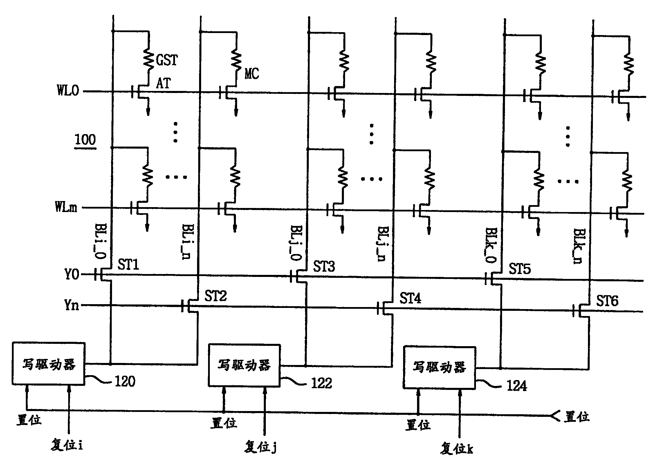
图5是依据本发明的某些实施例,被配置为提供连续复位脉冲的相变存储器设备100的示意图。如图5所示,相变存储器设备100包含多个相变存储器单元MC,其包括访问晶体管AT和包含相变材料的可变电阻GST。访问晶体管AT连接到相应的字线WL0到WLm以控制接通和关断访问晶体管AT。存储器单元还连接到相应的位线BLi_0...BLi_n、BLj_0...BLj_n以及BLk_0...BLk_n。还提供了相应的选择晶体管ST1、ST2、ST3、ST4、ST5和ST6,用于有选择地把位线连接到多个写驱动器电路120、122和124中的相应一个。FIG. 5 is a schematic diagram of a phase change memory device 100 configured to provide continuous reset pulses, in accordance with some embodiments of the present invention. As shown in FIG. 5 , the phase change memory device 100 includes a plurality of phase change memory cells MC including an access transistor AT and a variable resistor GST including a phase change material. The access transistor AT is connected to the corresponding word lines WL0 to WLm to control turning on and off of the access transistor AT. The memory cells are also connected to respective bit lines BLi_0...BLi_n, BLj_0...BLj_n, and BLk_0...BLk_n. Respective select transistors ST1 , ST2 , ST3 , ST4 , ST5 and ST6 are also provided for selectively connecting a bit line to a respective one of the plurality of write driver circuits 120 , 122 and 124 .
字线可以响应于行地址译码器(未显示),而且位线可以响应于列地址译码器(未显示)而被选择。这样的行和列地址译码器在本领域是众所周知的,因此不必在此处进行进一步的描述。此处使用的数据字是指,被选择用于行地址译码器和列地址译码器的给定输出的位数量(即,当字线有效,而且相应的列选择信号有效时)。在本发明的某些实施例中,字包含16个数据位。Word lines may be responsive to row address decoders (not shown), and bit lines may be selected responsive to column address decoders (not shown). Such row and column address decoders are well known in the art and thus need not be further described here. As used herein, a data word refers to the number of bits selected for a given output of the row and column address decoders (ie, when the word line is active and the corresponding column select signal is active). In some embodiments of the invention, a word contains 16 data bits.
此外,如图5所示,写驱动器可以与多条位线连接。多条位线可以来自不同的数据字。在其它实施例中,连接到写驱动器的某些或者全部位线可以来自相同的数据字。然而,如图5所示,连接到相应写驱动器120、122和124的位线来自不同的数据字。因此,在图5所示的实施例中,位线BLi_0到BLi_n表示n个数据字的第i位。在本发明的某些实施例中,四条位线和写驱动器120、122和124中的每个相连。In addition, as shown in FIG. 5, a write driver can be connected to a plurality of bit lines. Multiple bit lines can be from different data words. In other embodiments, some or all of the bit lines connected to the write driver may be from the same data word. However, as shown in FIG. 5, the bit lines connected to the respective write drivers 120, 122 and 124 are from different data words. Therefore, in the embodiment shown in FIG. 5, the bit lines BLi_0 to BLi_n represent the ith bit of n data words. In some embodiments of the invention, four bit lines are connected to each of write drivers 120 , 122 and 124 .
如图5中进一步所示,多个写驱动器120、122和124中的每个接收共用的置位信号和独立的复位信号RESET(复位)i、RESET(复位)j和RESET(复位)k。如图6所示,置位信号Set可以是具有相对长持续时间的信号,而且相应的复位信号RESET i、RESET j和RESET k每个具有较短的持续时间并且是按时间连续的。作为由复位信号发生器生成的连续复位脉冲,提供复位信号RESET i、RESET j和RESET k。在下面会进一步详细论述复位信号发生器的示例。因此,复位信号RESET i、RESET j和RESET k可以连续地施加到写驱动器120、122和124,使得不是全部用于数据字的写驱动器同时有效的,这可以减少当复位存储器单元时所需要的峰值电流。As further shown in FIG. 5, each of the plurality of write drivers 120, 122, and 124 receives a common set signal and independent reset signals RESETi, RESETj, and RESETk. As shown in FIG. 6, the set signal Set may be a signal having a relatively long duration, and the corresponding reset signals RESET i, RESET j, and RESET k each have a shorter duration and are sequential in time. The reset signals RESET i, RESET j, and RESET k are provided as successive reset pulses generated by the reset signal generator. Examples of reset signal generators are discussed in further detail below. Therefore, the reset signals RESET i, RESET j, and RESET k can be applied to the write drivers 120, 122, and 124 consecutively so that not all of the write drivers for the data word are active at the same time, which can reduce the time required when resetting a memory cell. peak current.
在本发明的某些实施例中,置位信号Set具有从大约100纳秒到大约500纳秒(ns)的持续时间,且连续的复位信号RESET i、RESET j和RESET k每个具有大约10纳秒到大约50纳秒的持续时间。连续的复位信号是不相重叠的,而且在实施例中,可以彼此间隔大约10纳秒。在本发明的某些实施例中,连续复位信号的持续时间总和小于置位信号的持续时间。通过使复位信号的持续时间总和不大于置位信号的持续时间,可以减少峰值复位电流,而不用延长为编程相变存储器设备的数据字所需花费的时间。此外虽然在图5和6中说明了三个复位信号,但是可以提供更少或者更多数量的复位信号。在本发明的某些实施例中,复位信号的数量受限于不让复位信号持续时间的总和超过置位信号持续时间而提供的复位信号数量。In some embodiments of the invention, the set signal Set has a duration of from about 100 nanoseconds to about 500 nanoseconds (ns), and successive reset signals RESET i, RESET j, and RESET k each have a duration of about 10 nanoseconds (ns). nanoseconds to approximately 50 nanoseconds in duration. Successive reset signals are non-overlapping and, in an embodiment, may be spaced approximately 10 nanoseconds apart from each other. In some embodiments of the invention, the sum of the durations of successive reset signals is less than the duration of the set signal. By having the sum of the durations of the reset signals not greater than the duration of the set signals, the peak reset current can be reduced without extending the time it takes to program a data word of the phase change memory device. Also, although three reset signals are illustrated in FIGS. 5 and 6, a fewer or greater number of reset signals may be provided. In some embodiments of the invention, the number of reset signals is limited to the number of reset signals provided without allowing the sum of the reset signal durations to exceed the set signal duration.
虽然图5中说明的实施例示出了三个写驱动器120、122和124,但是这样一个说明仅仅是相变存储器设备一部分的示例结构,而且可以提供更少或者更多数量的写驱动器。此外,虽然图5说明了每个具有单独复位信号的独立写驱动器,但是依据本发明的某些实施例,只要写驱动器组包含少于全部用于数据字的写驱动器,则这些组可以接收相同的信号。因此,例如相同数据字中的两个或更多写驱动器可以每个接收相同的复位信号。接收相同复位信号的写驱动器组可以是数量相同或者不相同的。例如,在本发明的某些实施例中,可以提供四个连续复位信号,每个都提供给四个写驱动器,以便在四组写驱动器中划分16位数据字。Although the embodiment illustrated in FIG. 5 shows three write drivers 120, 122, and 124, such an illustration is only an example structure of a portion of a phase change memory device, and fewer or greater numbers of write drivers may be provided. Additionally, although FIG. 5 illustrates separate write drivers each with a separate reset signal, groups of write drivers may receive the same signal of. Thus, for example, two or more write drivers in the same data word may each receive the same reset signal. The write driver groups receiving the same reset signal may be the same number or different. For example, in some embodiments of the invention, four consecutive reset signals may be provided, each to four write drivers, to divide the 16-bit data word among four groups of write drivers.
图7为依据本发明某些实施例的写驱动器电路的框图,该写驱动器电路可适合于用作写驱动器120、122和/或124。如图7所示,依据本发明某些实施例的写驱动器电路包含电流控制电路200、电流驱动器电路202和脉冲选择电路204。向电流控制电路200提供偏压DC_BIAS。电流控制电路200响应于脉冲选择电路204,并且控制电流驱动器202输出置位或者复位脉冲。脉冲选择电路204接收图6所示的连续复位脉冲中的一个和置位脉冲,以及要在相变存储器单元中编程的数据,并且使用该数据,以选择置位脉冲和连续复位脉冲中的一个。置位脉冲和连续复位脉冲中被选定的一个控制电流控制电路和电流驱动器,以在那时、和在实质上对应于该置位脉冲和连续复位脉冲中的选定一个的时序的持续时间内驱动位线。7 is a block diagram of a write driver circuit that may be suitable for use as write drivers 120, 122, and/or 124, in accordance with some embodiments of the present invention. As shown in FIG. 7 , the write driver circuit according to some embodiments of the present invention includes a
图8为依据本发明的某些实施例、图7中的写驱动器电路的更详细示意图。如图8所示,DATA(数据)输入在SET和RESETi输入之间进行选择,并且向电流控制电路200提供对应于SET和RESETi输入中被选择那个的信号。电流控制电路200通过控制驱动晶体管PM3,来控制由电流驱动器电路202提供的电流。FIG. 8 is a more detailed schematic diagram of the write driver circuit of FIG. 7 in accordance with some embodiments of the present invention. As shown in FIG. 8, the DATA (data) input selects between the SET and RESETi inputs and provides a signal to the
输出脉冲I_SET/I_RESETi的持续时间由反相器IN4的输出控制,使得当反相器IN4的输出处于高电平时,关断晶体管NM6和PM2,而且驱动晶体管PM3的控制是基于电流控制电路200的节点ND1的电压的。当反相器IN4的输出处于低电平时,接通晶体管PM2,其关断驱动晶体管PM3。当反相器IN4的输出为低电平时,反相器IN5的输出处于高电平,其接通晶体管NM6并且终止处于高电平的置位/复位脉冲I_SET/I_RESETi。反相器IN4的输出由SET和RESETi输入中的选定一个通过反相器IN3进行控制。因此,由写驱动器电路施加到位线的置位/复位脉冲I_SET/I_RESETi的持续时间可以由SET和RESETi输入中的选定一个的脉冲持续时间控制。The duration of the output pulse I_SET/I_RESETi is controlled by the output of the inverter IN4, so that when the output of the inverter IN4 is at a high level, the transistors NM6 and PM2 are turned off, and the control of the drive transistor PM3 is based on the
当DATA输入处于高电平、以便选择RESETi输入通过通过门PG2时,反相器IN1的输出为低,而且反相器IN2的输出为高。因此接通晶体管NM3和NM4。作为由DC_BIAS输入控制的结果,晶体管NM1和NM2总是接通。当RESETi信号处于高电平时,反相器IN4的输出处于高电平,其接通晶体管NM5并且关断晶体管PM2。流过晶体管NM1与NM2的电流i1和流过晶体管NM3与NM4的电流i2被镜像,使得在输出节点ND2提供复位电流i1+i2。当复位信号RESETi返回到低电平时,关断晶体管PM3并且接通晶体管NM6,以终止如上所述的复位脉冲。When the DATA input is high to select the RESETi input through pass gate PG2, the output of inverter IN1 is low and the output of inverter IN2 is high. Transistors NM3 and NM4 are thus turned on. Transistors NM1 and NM2 are always on as a result of being controlled by the DC_BIAS input. When the RESETi signal is high, the output of inverter IN4 is high, which turns on transistor NM5 and turns off transistor PM2. The current i1 flowing through the transistors NM1 and NM2 and the current i2 flowing through the transistors NM3 and NM4 are mirrored such that a reset current i1+i2 is provided at the output node ND2. When the reset signal RESETi returns to low level, the transistor PM3 is turned off and the transistor NM6 is turned on to terminate the reset pulse as described above.
当DATA输入处于低电平、以便选择SET输入通过通过门PG1时,反相器IN1的输出为高,而且反相器IN2的输出为低。因此,关断晶体管NM3和NM4。作为由DC_BIAS输入控制的结果,晶体管NM1和NM2总是接通。当SET信号处于高电平时,反相器IN4的输出处于高电平,其接通晶体管NM5并且关断晶体管PM2。仅仅流过晶体管NM1与NM2的电流i1被镜像,使得在输出节点ND2提供置位电流i1。当置位信号SET返回到低电平时,关断晶体管PM3并且接通晶体管NM6,以终止如上所述的置位脉冲。When the DATA input is low to select the SET input through pass gate PG1, the output of inverter IN1 is high and the output of inverter IN2 is low. Therefore, transistors NM3 and NM4 are turned off. Transistors NM1 and NM2 are always on as a result of being controlled by the DC_BIAS input. When the SET signal is at high level, the output of inverter IN4 is at high level, which turns on transistor NM5 and turns off transistor PM2. Only the current i1 flowing through the transistors NM1 and NM2 is mirrored such that a set current i1 is provided at the output node ND2. When the set signal SET returns to low level, the transistor PM3 is turned off and the transistor NM6 is turned on to terminate the set pulse as described above.
图9为依据本发明某些实施例的复位信号生成电路的示意图。如图9所示,可以响应于地址跃迁检测信号(ATD)生成复位脉冲。在本发明的其它实施例中,可以响应于数据跃迁检测信号(DTD)生成复位脉冲。ATD信号提供给起反相器作用的或非(NOR)门NOR1,使得当ATD信号为高时,或非门NOR1的输出为低,而且当ATD信号为低时,或非门NOR1的输出为高。或非门NOR1的输出连接到与非(NAND)门NAN1的输入和延迟元件D1。延迟元件D1可以用来控制连续复位脉冲的持续时间。因此,在本发明的某些实施例中,延迟元件D1提供了从大约10纳秒到大约50纳秒的脉冲。与非门NAN1的输出提供给多个串联连接的延迟元件D2、D3和D4,其中这些延迟元件的输出被提供作为多个连续复位脉冲的后续一个。在本发明的某些实施例中,延迟元件D2、D3和D4具有大于由与非门NAN1输出的脉冲的持续时间的延迟,以便提供不相重叠的连续脉冲。在某些实施例中,延迟元件D2、D3和D4的延迟,大于由与非门NAN1输出的脉冲的持续时间大约10纳秒。FIG. 9 is a schematic diagram of a reset signal generating circuit according to some embodiments of the present invention. As shown in FIG. 9, a reset pulse may be generated in response to an address transition detection signal (ATD). In other embodiments of the invention, the reset pulse may be generated in response to a data transition detect signal (DTD). The ATD signal is provided to the NOR gate NOR1, which acts as an inverter, so that when the ATD signal is high, the output of the NOR gate NOR1 is low, and when the ATD signal is low, the output of the NOR gate NOR1 is high. The output of the NOR gate NOR1 is connected to the input of the NAND gate NAN1 and the delay element D1. Delay element D1 can be used to control the duration of successive reset pulses. Thus, in some embodiments of the invention, delay element D1 provides a pulse of from about 10 nanoseconds to about 50 nanoseconds. The output of the NAND gate NAN1 is provided to a plurality of series connected delay elements D2, D3 and D4, wherein the output of these delay elements is provided as a subsequent one of a plurality of successive reset pulses. In some embodiments of the invention, delay elements D2, D3 and D4 have a delay greater than the duration of the pulses output by NAND gate NAN1 so as to provide non-overlapping consecutive pulses. In some embodiments, the delay of delay elements D2, D3 and D4 is about 10 nanoseconds greater than the duration of the pulse output by NAND gate NAN1.
图10为依据本发明进一步实施例的相变存储器设备300的一部分的示意图。如图10所示,可以如上参考图5所述提供相变存储器单元。然而,写驱动器电路320、322、324和326每个都连接到单条位线。在这种情况下,复位RESET1...RESETn和置位Set信号可以如图11所示提供。写驱动器电路320、322、324和326可以如上参考图7和8所述提供。此外,可以利用图9中的复位脉冲生成电路来向每个单独连接的写驱动器电路320、322、324和326提供连续复位脉冲。复位脉冲和置位脉冲的持续时间和关系可以如同上面参考图5和6所述。FIG. 10 is a schematic diagram of a portion of a phase change memory device 300 according to a further embodiment of the invention. As shown in FIG. 10 , a phase change memory cell may be provided as described above with reference to FIG. 5 . However, write driver circuits 320, 322, 324, and 326 are each connected to a single bit line. In this case, the reset RESET1...RESETn and set Set signals can be provided as shown in FIG. 11 . Write driver circuits 320 , 322 , 324 and 326 may be provided as described above with reference to FIGS. 7 and 8 . Additionally, the reset pulse generation circuit in FIG. 9 may be utilized to provide successive reset pulses to each individually connected write driver circuit 320 , 322 , 324 , and 326 . The duration and relationship of the reset and set pulses may be as described above with reference to FIGS. 5 and 6 .
操作中,图10的相变存储器设备300可以向相应的写驱动器电路320、322、324和326提供连续复位脉冲。因为复位脉冲被连续地施加到写驱动器电路320、322、324和326,由于可以减少同时驱动位线的写驱动器电路320、322、324和326的数量,可以减少复位相变存储器单元所需要的峰值电流。In operation, the phase change memory device 300 of FIG. 10 may provide successive reset pulses to respective write driver circuits 320 , 322 , 324 and 326 . Because the reset pulse is continuously applied to the write driver circuits 320, 322, 324, and 326, the number of write driver circuits 320, 322, 324, and 326 that simultaneously drive the bit lines can be reduced, and the time required to reset the phase change memory cells can be reduced. peak current.
如上所述,本发明的某些实施例可以提供相变存储器设备,其包含多个相变存储器单元和装置,这些装置用于向共同连接到字线的相变存储器单元的子集连续地施加复位脉冲。用于连续施加复位脉冲的装置可以例如由写驱动器电路120、122和124和/或320、322、324和326、图9中的脉冲生成电路、以及如上参考图5和/或10所述连接写驱动器电路到相变存储器单元的互连所提供。在本发明的特定实施例中,可以通过向多个相变存储器单元施加第一脉冲宽度的信号来复位这些相变存储器单元,以及通过向这些相变存储器单元施加第二脉冲宽度的信号来进行置位。在这种情况下,用于连续施加复位脉冲的装置可以包含以下这种用于连续施加复位脉冲的装置,其中,每一个连续施加的复位脉冲的持续时间对应于第一脉冲宽度,而且连续施加的复位脉冲的持续时间总和实质上不大于第二脉冲宽度。因此,可以减少峰值电流而没有增加用于写入数据字的编程时间。这样用于连续地施加复位脉冲的装置可以由延迟线结构、或者提供适当时序关系的其它这种脉冲生成电路所提供。As noted above, certain embodiments of the present invention may provide a phase change memory device comprising a plurality of phase change memory cells and means for sequentially applying reset pulse. The means for continuously applying reset pulses may for example consist of write driver circuits 120, 122 and 124 and/or 320, 322, 324 and 326, the pulse generation circuit in FIG. 9, and connections as described above with reference to FIGS. An interconnection of the write driver circuit to the phase change memory cell is provided. In a particular embodiment of the invention, the phase change memory cells may be reset by applying a signal of a first pulse width to the phase change memory cells, and by applying a signal of a second pulse width to the phase change memory cells. Position. In this case, the means for continuously applying reset pulses may comprise the following means for continuously applying reset pulses, wherein the duration of each successively applied reset pulse corresponds to the first pulse width, and the successively applied The sum of the durations of the reset pulses is substantially not greater than the second pulse width. Therefore, the peak current can be reduced without increasing the programming time for writing the data word. Such means for continuously applying reset pulses may be provided by delay line structures, or other such pulse generating circuits providing suitable timing relationships.
此外,本发明的某些实施例可以提供这样的装置,其向共同连接到字线的相变存储器单元的子集施加共用的置位脉冲。这样的装置可以例如由如上所述的置位脉冲生成电路到写驱动器电路的互连所提供。Furthermore, certain embodiments of the present invention may provide means for applying a common set pulse to a subset of phase change memory cells commonly connected to a word line. Such means may eg be provided by the interconnection of the set pulse generating circuit to the write driver circuit as described above.
虽然已经参考特定示例写驱动器电路和/或复位脉冲生成电路描述了本发明的实施例,但是可以利用其它用于提供连续施加的复位脉冲的技术和/或电路。例如,可以利用不使用延迟线的脉冲生成电路,或者任何提供了具有适当时序关系的期望连续脉冲的电路。此外,复位脉冲到位线的脉冲宽度和连续施加可以,例如通过在向写驱动器电路提供共用复位信号时连续激活访问晶体管ST1、ST3和ST5,以及通过控制访问晶体管有效的持续时间来控制复位脉冲持续时间,在写驱动器电路外部完成。Although embodiments of the invention have been described with reference to certain example write driver circuits and/or reset pulse generation circuits, other techniques and/or circuits for providing continuously applied reset pulses may be utilized. For example, a pulse generation circuit that does not use a delay line, or any circuit that provides the desired succession of pulses with the appropriate timing relationship, may be utilized. In addition, the pulse width and continuous application of the reset pulse to the bit line can be controlled, for example, by continuously activating the access transistors ST1, ST3 and ST5 when a common reset signal is provided to the write driver circuit, and by controlling the duration that the access transistors are active. time, done outside the write driver circuit.
本发明的实施例已经参考例如在写驱动器电路和脉冲生成电路之间的功能特定划分、或者在该写驱动器电路内的功能进行了描述。然而,可以对在框图中的块进行组合或者重新布置,但是其仍然在本发明的范围之内。因此,本发明的实施例不局限于上述的特定说明示例,而是可以包含能够执行此处描述的功能或者操作、用于连续地向相变存储器单元提供复位脉冲的任何电路。Embodiments of the invention have been described with reference to, for example, a specific division of functionality between the write driver circuit and the pulse generation circuit, or functionality within the write driver circuit. However, blocks in the block diagrams may be combined or rearranged while still remaining within the scope of the present invention. Accordingly, embodiments of the present invention are not limited to the particular illustrative examples described above, but may encompass any circuitry capable of performing the functions or operations described herein for continuously supplying reset pulses to phase change memory cells.
虽然已经参考本发明的说明性实施例具体示出和描述了本发明,但是本领域的技术人员应当理解,可以在其中进行各种形式和细节改变而不背离由权利要求所定义的本发明的精神和范围。While the invention has been particularly shown and described with reference to illustrative embodiments thereof, it will be understood by those skilled in the art that various changes in form and details may be made therein without departing from the spirit of the invention as defined by the claims. spirit and scope.
相关申请和优先权声明Related applications and priority claims
本申请涉及于2004年7月9日在韩国知识产权局提出的韩国专利申请2004-0053346,并要求它的优先权,而且它的公开内容通过引用全部包含在此。This application is related to and claims priority from Korean Patent Application No. 2004-0053346 filed in the Korean Intellectual Property Office on Jul. 9, 2004, the disclosure of which is hereby incorporated by reference in its entirety.
Claims (31)
Applications Claiming Priority (4)
| Application Number | Priority Date | Filing Date | Title |
|---|---|---|---|
| KR53346/04 | 2004-07-09 | ||
| KR1020040053346A KR100587702B1 (en) | 2004-07-09 | 2004-07-09 | Phase change memory device having peak current reduction characteristics and data writing method accordingly |
| US11/074,557 US7304885B2 (en) | 2004-07-09 | 2005-03-08 | Phase change memories and/or methods of programming phase change memories using sequential reset control |
| US11/074,557 | 2005-03-08 |
Publications (2)
| Publication Number | Publication Date |
|---|---|
| CN1734671A CN1734671A (en) | 2006-02-15 |
| CN1734671B true CN1734671B (en) | 2010-04-21 |
Family
ID=36077005
Family Applications (1)
| Application Number | Title | Priority Date | Filing Date |
|---|---|---|---|
| CN200510077929.5A Expired - Fee Related CN1734671B (en) | 2004-07-09 | 2005-06-15 | Phase change memory and method of programming phase change memory using continuous reset control |
Country Status (6)
| Country | Link |
|---|---|
| US (4) | US7304885B2 (en) |
| EP (1) | EP1617437B1 (en) |
| JP (1) | JP4832817B2 (en) |
| KR (1) | KR100587702B1 (en) |
| CN (1) | CN1734671B (en) |
| TW (1) | TWI371753B (en) |
Families Citing this family (60)
| Publication number | Priority date | Publication date | Assignee | Title |
|---|---|---|---|---|
| KR100587702B1 (en) * | 2004-07-09 | 2006-06-08 | 삼성전자주식회사 | Phase change memory device having peak current reduction characteristics and data writing method accordingly |
| WO2006043230A1 (en) * | 2004-10-21 | 2006-04-27 | Koninklijke Philips Electronics N.V. | Integrated circuit with phase-change memory cells and method for addressing phase-change memory cells |
| US7460389B2 (en) * | 2005-07-29 | 2008-12-02 | International Business Machines Corporation | Write operations for phase-change-material memory |
| US7548448B2 (en) * | 2005-08-24 | 2009-06-16 | Infineon Technologies Ag | Integrated circuit having a switch |
| KR100816748B1 (en) | 2006-03-16 | 2008-03-27 | 삼성전자주식회사 | Phase change memory device supporting program suspend / resume mode and its programming method |
| US7499316B2 (en) | 2006-03-31 | 2009-03-03 | Samsung Electronics Co., Ltd. | Phase change memory devices and program methods |
| KR100857742B1 (en) | 2006-03-31 | 2008-09-10 | 삼성전자주식회사 | Phase Change Memory Device and Method applying Program Current Thereof |
| KR100719383B1 (en) * | 2006-04-12 | 2007-05-18 | 삼성전자주식회사 | Phase change memory device using multi-program method |
| KR100763231B1 (en) * | 2006-09-11 | 2007-10-04 | 삼성전자주식회사 | Phase change memory device |
| US7885102B2 (en) | 2006-09-15 | 2011-02-08 | Renesas Electronics Corporation | Semiconductor device |
| JP4328796B2 (en) | 2006-10-31 | 2009-09-09 | エルピーダメモリ株式会社 | Semiconductor memory device and write control method thereof |
| US7679980B2 (en) * | 2006-11-21 | 2010-03-16 | Qimonda North America Corp. | Resistive memory including selective refresh operation |
| KR100827703B1 (en) * | 2006-12-14 | 2008-05-07 | 삼성전자주식회사 | Test method of phase change memory device |
| US7760545B2 (en) * | 2006-12-26 | 2010-07-20 | Elpida Memory, Inc. | Semiconductor memory device and programming method thereof |
| JP5490357B2 (en) | 2007-04-04 | 2014-05-14 | ピーエスフォー ルクスコ エスエイアールエル | Semiconductor memory device and control method thereof |
| JP5413938B2 (en) | 2007-05-08 | 2014-02-12 | ピーエスフォー ルクスコ エスエイアールエル | Semiconductor memory device and write control method thereof |
| KR101274190B1 (en) * | 2007-07-30 | 2013-06-14 | 삼성전자주식회사 | Nonvolatile memory device using variable resistive element |
| JP5420828B2 (en) * | 2007-08-24 | 2014-02-19 | ピーエスフォー ルクスコ エスエイアールエル | Semiconductor memory device and write control method thereof |
| JP2009104716A (en) * | 2007-10-24 | 2009-05-14 | Toshiba Corp | Resistance change memory device and data erasing method thereof |
| KR101291222B1 (en) * | 2007-11-29 | 2013-07-31 | 삼성전자주식회사 | Method of operating phase change memory device |
| KR100900121B1 (en) * | 2007-11-30 | 2009-06-01 | 주식회사 하이닉스반도체 | Semiconductor memory device |
| KR100895400B1 (en) * | 2007-12-03 | 2009-05-06 | 주식회사 하이닉스반도체 | Phase change memory device |
| KR100858688B1 (en) * | 2007-12-06 | 2008-09-16 | 한양대학교 산학협력단 | Nonvolatile Memory and How to Read It |
| KR101339288B1 (en) | 2007-12-14 | 2013-12-09 | 삼성전자 주식회사 | Nonvolatile memory device using variable resistive element |
| US8964488B2 (en) | 2007-12-14 | 2015-02-24 | Samsung Electronics Co., Ltd. | Non-volatile memory device using variable resistance element with an improved write performance |
| US7889536B2 (en) * | 2007-12-17 | 2011-02-15 | Qimonda Ag | Integrated circuit including quench devices |
| JP5474313B2 (en) * | 2008-04-25 | 2014-04-16 | ピーエスフォー ルクスコ エスエイアールエル | Semiconductor memory device and control method thereof |
| US8134857B2 (en) * | 2008-06-27 | 2012-03-13 | Macronix International Co., Ltd. | Methods for high speed reading operation of phase change memory and device employing same |
| IT1393759B1 (en) * | 2008-07-28 | 2012-05-08 | Stmicroelectronics Rousset | PROGRAMMING DEVICE FOR A PCM MEMORY CELL WITH DISCHARGE OF CAPACITY AND METHOD FOR PROGRAMMING A PCM MEMORY CELL |
| JP5106297B2 (en) | 2008-07-30 | 2012-12-26 | 株式会社東芝 | Semiconductor memory device |
| KR101453969B1 (en) | 2008-07-31 | 2014-10-22 | 삼성전자주식회사 | Resistive memory device and writing method thereof |
| US8027209B2 (en) * | 2008-10-06 | 2011-09-27 | Sandisk 3D, Llc | Continuous programming of non-volatile memory |
| JP2010170607A (en) | 2009-01-21 | 2010-08-05 | Elpida Memory Inc | Semiconductor memory device |
| JP4720912B2 (en) * | 2009-01-22 | 2011-07-13 | ソニー株式会社 | Resistance change memory device |
| KR20100097407A (en) * | 2009-02-26 | 2010-09-03 | 삼성전자주식회사 | Resistive memory device, memory system including the same, and programming method of the same |
| KR100996185B1 (en) * | 2009-03-16 | 2010-11-25 | 주식회사 하이닉스반도체 | Phase change memory device |
| KR20100107609A (en) * | 2009-03-26 | 2010-10-06 | 삼성전자주식회사 | Resistive memory device, memory system including the same, and writing method of the same |
| US8239629B2 (en) * | 2009-03-31 | 2012-08-07 | Micron Technology, Inc. | Hierarchical memory architecture to connect mass storage devices |
| US20110051485A1 (en) * | 2009-08-28 | 2011-03-03 | International Business Machines Corporation | Content addressable memory array writing |
| US7948782B2 (en) * | 2009-08-28 | 2011-05-24 | International Business Machines Corporation | Content addressable memory reference clock |
| US8804411B1 (en) | 2009-09-11 | 2014-08-12 | Micron Technology, Inc | Dual mode clock and data scheme for memory programming |
| US8107276B2 (en) * | 2009-12-04 | 2012-01-31 | International Business Machines Corporation | Resistive memory devices having a not-and (NAND) structure |
| CN103222005B (en) | 2009-12-31 | 2016-08-24 | 美光科技公司 | Method for phase change memory array |
| JP2011204288A (en) * | 2010-03-24 | 2011-10-13 | Toshiba Corp | Nonvolatile semiconductor memory device |
| US8570828B2 (en) * | 2010-04-12 | 2013-10-29 | Mosaid Technologies Incorporated | Memory programming using variable data width |
| US8497705B2 (en) * | 2010-11-09 | 2013-07-30 | Macronix International Co., Ltd. | Phase change device for interconnection of programmable logic device |
| US8909849B2 (en) * | 2010-11-15 | 2014-12-09 | Intel Corporation | Pipeline architecture for scalable performance on memory |
| KR20130058533A (en) * | 2011-11-25 | 2013-06-04 | 에스케이하이닉스 주식회사 | Phase change memory device and data storage device including the same |
| KR101970314B1 (en) * | 2012-04-10 | 2019-04-18 | 삼성전자주식회사 | Non-volatile memory device, operating method thereof, and electronic device having the same |
| KR102154296B1 (en) | 2012-12-18 | 2020-09-14 | 삼성전자 주식회사 | A driving method of nonvolatile memory device using variable resistive element and the nonvolatile memory device |
| CN102982841A (en) * | 2012-12-18 | 2013-03-20 | 中国科学院上海微系统与信息技术研究所 | Programming system and method of phase change memory |
| KR102151183B1 (en) * | 2014-06-30 | 2020-09-02 | 삼성전자주식회사 | Resistive Memory Device and Operating Method thereof |
| US9711213B2 (en) | 2014-09-04 | 2017-07-18 | Micron Technology, Inc. | Operational signals generated from capacitive stored charge |
| KR102217243B1 (en) * | 2014-10-28 | 2021-02-18 | 삼성전자주식회사 | Resistive Memory Device, Resistive Memory System and Operating Method thereof |
| US9613696B1 (en) * | 2015-12-16 | 2017-04-04 | Stmicroelectronics International N.V. | Memory device including decoder for a program pulse and related methods |
| JP6249029B2 (en) * | 2016-03-08 | 2017-12-20 | Nttエレクトロニクス株式会社 | Data phase tracking device, data phase tracking method, and communication device |
| KR20180032391A (en) * | 2016-09-22 | 2018-03-30 | 에스케이하이닉스 주식회사 | Semiconductor Memory Apparatus |
| KR102067112B1 (en) * | 2017-10-17 | 2020-01-16 | 한양대학교 산학협력단 | Neuron network semiconductor device based on phase change material |
| CN112102858B (en) * | 2019-02-27 | 2023-02-03 | 北京时代全芯存储技术股份有限公司 | Memory write method |
| US11410722B2 (en) * | 2020-10-21 | 2022-08-09 | Samsung Electronics Co., Ltd. | Phase-change memory device for improving resistance drift and dynamic resistance drift compensation method of the same |
Citations (3)
| Publication number | Priority date | Publication date | Assignee | Title |
|---|---|---|---|---|
| US6480438B1 (en) * | 2001-06-12 | 2002-11-12 | Ovonyx, Inc. | Providing equal cell programming conditions across a large and high density array of phase-change memory cells |
| US6487113B1 (en) * | 2001-06-29 | 2002-11-26 | Ovonyx, Inc. | Programming a phase-change memory with slow quench time |
| US6707712B2 (en) * | 2001-08-02 | 2004-03-16 | Intel Corporation | Method for reading a structural phase-change memory |
Family Cites Families (21)
| Publication number | Priority date | Publication date | Assignee | Title |
|---|---|---|---|---|
| US3922648A (en) * | 1974-08-19 | 1975-11-25 | Energy Conversion Devices Inc | Method and means for preventing degradation of threshold voltage of filament-forming memory semiconductor device |
| JP2845952B2 (en) * | 1989-06-28 | 1999-01-13 | 株式会社日立製作所 | Thin film magnetic memory cell and its recording and reproducing apparatus |
| US6256224B1 (en) * | 2000-05-03 | 2001-07-03 | Hewlett-Packard Co | Write circuit for large MRAM arrays |
| JP3720983B2 (en) * | 1998-06-23 | 2005-11-30 | 株式会社東芝 | Ferroelectric memory |
| US6075719A (en) | 1999-06-22 | 2000-06-13 | Energy Conversion Devices, Inc. | Method of programming phase-change memory element |
| KR100322470B1 (en) * | 1999-07-22 | 2002-02-07 | 윤종용 | High-density nor-type flash memory device and a programming method thereof |
| US6236611B1 (en) * | 1999-12-20 | 2001-05-22 | Motorola, Inc. | Peak program current reduction apparatus and method |
| US6426893B1 (en) | 2000-02-17 | 2002-07-30 | Sandisk Corporation | Flash eeprom system with simultaneous multiple data sector programming and storage of physical block characteristics in other designated blocks |
| JP3620434B2 (en) | 2000-07-26 | 2005-02-16 | 株式会社日立製作所 | Information processing system |
| US6504196B1 (en) | 2001-08-30 | 2003-01-07 | Micron Technology, Inc. | CMOS imager and method of formation |
| US6545907B1 (en) | 2001-10-30 | 2003-04-08 | Ovonyx, Inc. | Technique and apparatus for performing write operations to a phase change material memory device |
| US6768665B2 (en) | 2002-08-05 | 2004-07-27 | Intel Corporation | Refreshing memory cells of a phase change material memory device |
| US6839270B2 (en) * | 2003-01-17 | 2005-01-04 | Hewlett-Packard Development Company, L.P. | System for and method of accessing a four-conductor magnetic random access memory |
| JP4331966B2 (en) | 2003-04-14 | 2009-09-16 | 株式会社ルネサステクノロジ | Semiconductor integrated circuit |
| EP1489622B1 (en) * | 2003-06-16 | 2007-08-15 | STMicroelectronics S.r.l. | Writing circuit for a phase change memory device |
| KR100642187B1 (en) * | 2003-09-08 | 2006-11-10 | 가부시끼가이샤 도시바 | Non-volatile semiconductor memory device, electronic card, and electronic device |
| US7283384B1 (en) * | 2004-03-24 | 2007-10-16 | Silicon Magnetic Systems | Magnetic memory array architecture |
| JP4256305B2 (en) | 2004-06-09 | 2009-04-22 | 株式会社東芝 | Semiconductor memory device |
| KR100587702B1 (en) * | 2004-07-09 | 2006-06-08 | 삼성전자주식회사 | Phase change memory device having peak current reduction characteristics and data writing method accordingly |
| US7113424B2 (en) * | 2004-11-23 | 2006-09-26 | Infineon Technologies Ag | Energy adjusted write pulses in phase-change memories |
| US7099180B1 (en) * | 2005-02-15 | 2006-08-29 | Intel Corporation | Phase change memory bits reset through a series of pulses of increasing amplitude |
-
2004
- 2004-07-09 KR KR1020040053346A patent/KR100587702B1/en not_active Expired - Fee Related
-
2005
- 2005-03-08 US US11/074,557 patent/US7304885B2/en not_active Expired - Lifetime
- 2005-05-13 TW TW094115509A patent/TWI371753B/en not_active IP Right Cessation
- 2005-06-15 CN CN200510077929.5A patent/CN1734671B/en not_active Expired - Fee Related
- 2005-07-06 EP EP05014605A patent/EP1617437B1/en not_active Expired - Lifetime
- 2005-07-11 JP JP2005202252A patent/JP4832817B2/en not_active Expired - Fee Related
-
2007
- 2007-12-03 US US11/949,342 patent/US7643335B2/en not_active Expired - Fee Related
-
2009
- 2009-11-03 US US12/611,606 patent/US7944741B2/en not_active Expired - Fee Related
-
2011
- 2011-04-21 US US13/091,238 patent/US8194442B2/en not_active Expired - Fee Related
Patent Citations (3)
| Publication number | Priority date | Publication date | Assignee | Title |
|---|---|---|---|---|
| US6480438B1 (en) * | 2001-06-12 | 2002-11-12 | Ovonyx, Inc. | Providing equal cell programming conditions across a large and high density array of phase-change memory cells |
| US6487113B1 (en) * | 2001-06-29 | 2002-11-26 | Ovonyx, Inc. | Programming a phase-change memory with slow quench time |
| US6707712B2 (en) * | 2001-08-02 | 2004-03-16 | Intel Corporation | Method for reading a structural phase-change memory |
Also Published As
| Publication number | Publication date |
|---|---|
| US20080137402A1 (en) | 2008-06-12 |
| JP4832817B2 (en) | 2011-12-07 |
| US7643335B2 (en) | 2010-01-05 |
| CN1734671A (en) | 2006-02-15 |
| US20100097850A1 (en) | 2010-04-22 |
| TW200603154A (en) | 2006-01-16 |
| TWI371753B (en) | 2012-09-01 |
| KR100587702B1 (en) | 2006-06-08 |
| US20110242886A1 (en) | 2011-10-06 |
| JP2006024355A (en) | 2006-01-26 |
| US7944741B2 (en) | 2011-05-17 |
| US20060007729A1 (en) | 2006-01-12 |
| KR20060004289A (en) | 2006-01-12 |
| EP1617437A1 (en) | 2006-01-18 |
| US7304885B2 (en) | 2007-12-04 |
| EP1617437B1 (en) | 2013-03-20 |
| US8194442B2 (en) | 2012-06-05 |
Similar Documents
| Publication | Publication Date | Title |
|---|---|---|
| CN1734671B (en) | Phase change memory and method of programming phase change memory using continuous reset control | |
| US7535746B2 (en) | Nonvolatile semiconductor memory device and read method | |
| US8537598B2 (en) | Nonvolatile semiconductor memory device and method for resetting the same | |
| JP5384653B2 (en) | Continuous programming of non-volatile memory | |
| JP5268481B2 (en) | Nonvolatile semiconductor memory device | |
| US7349245B2 (en) | Non-volatile phase-change memory device and associated program-suspend-read operation | |
| US8014190B2 (en) | Resistance variable memory device and method of writing data | |
| US7911824B2 (en) | Nonvolatile memory apparatus | |
| CN1697082B (en) | Method for programming phase-change memory array to set state and memory device circuit | |
| US7436693B2 (en) | Phase-change semiconductor memory device and method of programming the same | |
| CN104123960B (en) | Resistive memory device and its operating method | |
| US8391047B2 (en) | Method of executing a forming operation to variable resistance element | |
| CN1897156B (en) | Phase change random access memory with variable driving voltage | |
| US7787316B2 (en) | Semiconductor memory device and write control method thereof | |
| EP1835508B1 (en) | Pram and associated operation method and system | |
| JP2006127583A (en) | Nonvolatile semiconductor memory device and phase change memory | |
| JP2011108327A (en) | Non-volatile semiconductor memory device | |
| EP2422345A1 (en) | Memory system with data line switching scheme | |
| CN103703514B (en) | Three-dimensional memory system with column pipeline | |
| JP5416079B2 (en) | Semiconductor memory device and memory module | |
| US7755952B2 (en) | Semiconductor memory device and writing control method thereof | |
| US7710790B2 (en) | Semiconductor memory device and write control method thereof | |
| JP5568674B2 (en) | Semiconductor memory device |
Legal Events
| Date | Code | Title | Description |
|---|---|---|---|
| C06 | Publication | ||
| PB01 | Publication | ||
| C10 | Entry into substantive examination | ||
| SE01 | Entry into force of request for substantive examination | ||
| C14 | Grant of patent or utility model | ||
| GR01 | Patent grant | ||
| CF01 | Termination of patent right due to non-payment of annual fee | ||
| CF01 | Termination of patent right due to non-payment of annual fee |
Granted publication date: 20100421 Termination date: 20210615 |