CN1663044A - Lamps and methods of making them - Google Patents
Lamps and methods of making them Download PDFInfo
- Publication number
- CN1663044A CN1663044A CN038138530A CN03813853A CN1663044A CN 1663044 A CN1663044 A CN 1663044A CN 038138530 A CN038138530 A CN 038138530A CN 03813853 A CN03813853 A CN 03813853A CN 1663044 A CN1663044 A CN 1663044A
- Authority
- CN
- China
- Prior art keywords
- light
- conductors
- lamp
- support structure
- cup
- Prior art date
- Legal status (The legal status is an assumption and is not a legal conclusion. Google has not performed a legal analysis and makes no representation as to the accuracy of the status listed.)
- Pending
Links
- 238000000034 method Methods 0.000 title claims description 49
- 239000004020 conductor Substances 0.000 claims description 105
- BQCADISMDOOEFD-UHFFFAOYSA-N Silver Chemical compound [Ag] BQCADISMDOOEFD-UHFFFAOYSA-N 0.000 claims description 14
- 229910052709 silver Inorganic materials 0.000 claims description 14
- 239000004332 silver Substances 0.000 claims description 14
- RYGMFSIKBFXOCR-UHFFFAOYSA-N Copper Chemical compound [Cu] RYGMFSIKBFXOCR-UHFFFAOYSA-N 0.000 claims description 7
- 229910052802 copper Inorganic materials 0.000 claims description 7
- 239000010949 copper Substances 0.000 claims description 7
- 229910001316 Ag alloy Inorganic materials 0.000 claims description 6
- 229910000881 Cu alloy Inorganic materials 0.000 claims description 4
- 238000000465 moulding Methods 0.000 claims description 3
- 238000004806 packaging method and process Methods 0.000 claims description 2
- 239000011248 coating agent Substances 0.000 claims 1
- 238000000576 coating method Methods 0.000 claims 1
- 230000008878 coupling Effects 0.000 claims 1
- 238000010168 coupling process Methods 0.000 claims 1
- 238000005859 coupling reaction Methods 0.000 claims 1
- 238000004519 manufacturing process Methods 0.000 abstract description 17
- 229910052751 metal Inorganic materials 0.000 abstract description 7
- 239000002184 metal Substances 0.000 abstract description 7
- 239000000463 material Substances 0.000 description 18
- 230000008569 process Effects 0.000 description 13
- 239000004593 Epoxy Substances 0.000 description 10
- 238000007747 plating Methods 0.000 description 9
- 239000003086 colorant Substances 0.000 description 6
- OAICVXFJPJFONN-UHFFFAOYSA-N Phosphorus Chemical compound [P] OAICVXFJPJFONN-UHFFFAOYSA-N 0.000 description 5
- 229910052782 aluminium Inorganic materials 0.000 description 5
- XAGFODPZIPBFFR-UHFFFAOYSA-N aluminium Chemical compound [Al] XAGFODPZIPBFFR-UHFFFAOYSA-N 0.000 description 5
- 230000000712 assembly Effects 0.000 description 5
- 238000000429 assembly Methods 0.000 description 5
- 230000005284 excitation Effects 0.000 description 5
- 238000012545 processing Methods 0.000 description 5
- 238000009713 electroplating Methods 0.000 description 4
- 239000000843 powder Substances 0.000 description 4
- 238000000926 separation method Methods 0.000 description 4
- 229920001169 thermoplastic Polymers 0.000 description 4
- 239000004416 thermosoftening plastic Substances 0.000 description 4
- 238000003466 welding Methods 0.000 description 4
- 238000003491 array Methods 0.000 description 3
- 230000000295 complement effect Effects 0.000 description 3
- 238000013461 design Methods 0.000 description 3
- 238000006073 displacement reaction Methods 0.000 description 3
- 238000005516 engineering process Methods 0.000 description 3
- 238000003754 machining Methods 0.000 description 3
- 230000007246 mechanism Effects 0.000 description 3
- 230000003287 optical effect Effects 0.000 description 3
- 230000011218 segmentation Effects 0.000 description 3
- 238000007740 vapor deposition Methods 0.000 description 3
- 239000000853 adhesive Substances 0.000 description 2
- 238000004026 adhesive bonding Methods 0.000 description 2
- 230000001070 adhesive effect Effects 0.000 description 2
- 230000008859 change Effects 0.000 description 2
- 238000000748 compression moulding Methods 0.000 description 2
- 238000007796 conventional method Methods 0.000 description 2
- 238000010586 diagram Methods 0.000 description 2
- 238000009826 distribution Methods 0.000 description 2
- 238000005538 encapsulation Methods 0.000 description 2
- 239000003822 epoxy resin Substances 0.000 description 2
- 238000005530 etching Methods 0.000 description 2
- 239000003292 glue Substances 0.000 description 2
- PCHJSUWPFVWCPO-UHFFFAOYSA-N gold Chemical compound [Au] PCHJSUWPFVWCPO-UHFFFAOYSA-N 0.000 description 2
- 230000017525 heat dissipation Effects 0.000 description 2
- 238000003780 insertion Methods 0.000 description 2
- 230000037431 insertion Effects 0.000 description 2
- 229920000647 polyepoxide Polymers 0.000 description 2
- 239000011347 resin Substances 0.000 description 2
- 229920005989 resin Polymers 0.000 description 2
- 238000005476 soldering Methods 0.000 description 2
- 238000001429 visible spectrum Methods 0.000 description 2
- OKTJSMMVPCPJKN-UHFFFAOYSA-N Carbon Chemical compound [C] OKTJSMMVPCPJKN-UHFFFAOYSA-N 0.000 description 1
- 229910000978 Pb alloy Inorganic materials 0.000 description 1
- 229920005372 Plexiglas® Polymers 0.000 description 1
- 229910001128 Sn alloy Inorganic materials 0.000 description 1
- 239000011358 absorbing material Substances 0.000 description 1
- 238000013459 approach Methods 0.000 description 1
- 230000008901 benefit Effects 0.000 description 1
- 239000011230 binding agent Substances 0.000 description 1
- 230000015572 biosynthetic process Effects 0.000 description 1
- 239000003054 catalyst Substances 0.000 description 1
- 150000001875 compounds Chemical class 0.000 description 1
- 238000005520 cutting process Methods 0.000 description 1
- 238000011161 development Methods 0.000 description 1
- 230000018109 developmental process Effects 0.000 description 1
- 238000009792 diffusion process Methods 0.000 description 1
- 230000000694 effects Effects 0.000 description 1
- 238000010292 electrical insulation Methods 0.000 description 1
- 239000010931 gold Substances 0.000 description 1
- 229910052737 gold Inorganic materials 0.000 description 1
- LNEPOXFFQSENCJ-UHFFFAOYSA-N haloperidol Chemical compound C1CC(O)(C=2C=CC(Cl)=CC=2)CCN1CCCC(=O)C1=CC=C(F)C=C1 LNEPOXFFQSENCJ-UHFFFAOYSA-N 0.000 description 1
- 238000010438 heat treatment Methods 0.000 description 1
- BHEPBYXIRTUNPN-UHFFFAOYSA-N hydridophosphorus(.) (triplet) Chemical compound [PH] BHEPBYXIRTUNPN-UHFFFAOYSA-N 0.000 description 1
- 238000005286 illumination Methods 0.000 description 1
- 230000006872 improvement Effects 0.000 description 1
- 239000011810 insulating material Substances 0.000 description 1
- 230000031700 light absorption Effects 0.000 description 1
- 238000001465 metallisation Methods 0.000 description 1
- 238000012986 modification Methods 0.000 description 1
- 230000004048 modification Effects 0.000 description 1
- 229910052698 phosphorus Inorganic materials 0.000 description 1
- 239000011574 phosphorus Substances 0.000 description 1
- 238000005498 polishing Methods 0.000 description 1
- 239000004926 polymethyl methacrylate Substances 0.000 description 1
- 238000004080 punching Methods 0.000 description 1
- 239000004065 semiconductor Substances 0.000 description 1
- 229910000679 solder Inorganic materials 0.000 description 1
- 239000007787 solid Substances 0.000 description 1
- 239000000758 substrate Substances 0.000 description 1
- 238000009827 uniform distribution Methods 0.000 description 1
Images


Classifications
-
- H—ELECTRICITY
- H10—SEMICONDUCTOR DEVICES; ELECTRIC SOLID-STATE DEVICES NOT OTHERWISE PROVIDED FOR
- H10H—INORGANIC LIGHT-EMITTING SEMICONDUCTOR DEVICES HAVING POTENTIAL BARRIERS
- H10H20/00—Individual inorganic light-emitting semiconductor devices having potential barriers, e.g. light-emitting diodes [LED]
- H10H20/80—Constructional details
- H10H20/85—Packages
- H10H20/857—Interconnections, e.g. lead-frames, bond wires or solder balls
-
- F—MECHANICAL ENGINEERING; LIGHTING; HEATING; WEAPONS; BLASTING
- F21—LIGHTING
- F21K—NON-ELECTRIC LIGHT SOURCES USING LUMINESCENCE; LIGHT SOURCES USING ELECTROCHEMILUMINESCENCE; LIGHT SOURCES USING CHARGES OF COMBUSTIBLE MATERIAL; LIGHT SOURCES USING SEMICONDUCTOR DEVICES AS LIGHT-GENERATING ELEMENTS; LIGHT SOURCES NOT OTHERWISE PROVIDED FOR
- F21K9/00—Light sources using semiconductor devices as light-generating elements, e.g. using light-emitting diodes [LED] or lasers
-
- H—ELECTRICITY
- H01—ELECTRIC ELEMENTS
- H01L—SEMICONDUCTOR DEVICES NOT COVERED BY CLASS H10
- H01L25/00—Assemblies consisting of a plurality of semiconductor or other solid state devices
- H01L25/03—Assemblies consisting of a plurality of semiconductor or other solid state devices all the devices being of a type provided for in a single subclass of subclasses H10B, H10F, H10H, H10K or H10N, e.g. assemblies of rectifier diodes
- H01L25/04—Assemblies consisting of a plurality of semiconductor or other solid state devices all the devices being of a type provided for in a single subclass of subclasses H10B, H10F, H10H, H10K or H10N, e.g. assemblies of rectifier diodes the devices not having separate containers
- H01L25/075—Assemblies consisting of a plurality of semiconductor or other solid state devices all the devices being of a type provided for in a single subclass of subclasses H10B, H10F, H10H, H10K or H10N, e.g. assemblies of rectifier diodes the devices not having separate containers the devices being of a type provided for in group H10H20/00
- H01L25/0753—Assemblies consisting of a plurality of semiconductor or other solid state devices all the devices being of a type provided for in a single subclass of subclasses H10B, H10F, H10H, H10K or H10N, e.g. assemblies of rectifier diodes the devices not having separate containers the devices being of a type provided for in group H10H20/00 the devices being arranged next to each other
-
- F—MECHANICAL ENGINEERING; LIGHTING; HEATING; WEAPONS; BLASTING
- F21—LIGHTING
- F21Y—INDEXING SCHEME ASSOCIATED WITH SUBCLASSES F21K, F21L, F21S and F21V, RELATING TO THE FORM OR THE KIND OF THE LIGHT SOURCES OR OF THE COLOUR OF THE LIGHT EMITTED
- F21Y2107/00—Light sources with three-dimensionally disposed light-generating elements
- F21Y2107/20—Light sources with three-dimensionally disposed light-generating elements on convex supports or substrates, e.g. on the outer surface of spheres
-
- F—MECHANICAL ENGINEERING; LIGHTING; HEATING; WEAPONS; BLASTING
- F21—LIGHTING
- F21Y—INDEXING SCHEME ASSOCIATED WITH SUBCLASSES F21K, F21L, F21S and F21V, RELATING TO THE FORM OR THE KIND OF THE LIGHT SOURCES OR OF THE COLOUR OF THE LIGHT EMITTED
- F21Y2115/00—Light-generating elements of semiconductor light sources
- F21Y2115/10—Light-emitting diodes [LED]
-
- H—ELECTRICITY
- H01—ELECTRIC ELEMENTS
- H01L—SEMICONDUCTOR DEVICES NOT COVERED BY CLASS H10
- H01L2224/00—Indexing scheme for arrangements for connecting or disconnecting semiconductor or solid-state bodies and methods related thereto as covered by H01L24/00
- H01L2224/01—Means for bonding being attached to, or being formed on, the surface to be connected, e.g. chip-to-package, die-attach, "first-level" interconnects; Manufacturing methods related thereto
- H01L2224/42—Wire connectors; Manufacturing methods related thereto
- H01L2224/44—Structure, shape, material or disposition of the wire connectors prior to the connecting process
- H01L2224/45—Structure, shape, material or disposition of the wire connectors prior to the connecting process of an individual wire connector
- H01L2224/45001—Core members of the connector
- H01L2224/45099—Material
- H01L2224/451—Material with a principal constituent of the material being a metal or a metalloid, e.g. boron (B), silicon (Si), germanium (Ge), arsenic (As), antimony (Sb), tellurium (Te) and polonium (Po), and alloys thereof
- H01L2224/45138—Material with a principal constituent of the material being a metal or a metalloid, e.g. boron (B), silicon (Si), germanium (Ge), arsenic (As), antimony (Sb), tellurium (Te) and polonium (Po), and alloys thereof the principal constituent melting at a temperature of greater than or equal to 950°C and less than 1550°C
- H01L2224/45144—Gold (Au) as principal constituent
-
- H—ELECTRICITY
- H01—ELECTRIC ELEMENTS
- H01L—SEMICONDUCTOR DEVICES NOT COVERED BY CLASS H10
- H01L2224/00—Indexing scheme for arrangements for connecting or disconnecting semiconductor or solid-state bodies and methods related thereto as covered by H01L24/00
- H01L2224/01—Means for bonding being attached to, or being formed on, the surface to be connected, e.g. chip-to-package, die-attach, "first-level" interconnects; Manufacturing methods related thereto
- H01L2224/42—Wire connectors; Manufacturing methods related thereto
- H01L2224/47—Structure, shape, material or disposition of the wire connectors after the connecting process
- H01L2224/48—Structure, shape, material or disposition of the wire connectors after the connecting process of an individual wire connector
- H01L2224/4805—Shape
- H01L2224/4809—Loop shape
- H01L2224/48091—Arched
-
- H—ELECTRICITY
- H01—ELECTRIC ELEMENTS
- H01L—SEMICONDUCTOR DEVICES NOT COVERED BY CLASS H10
- H01L2924/00—Indexing scheme for arrangements or methods for connecting or disconnecting semiconductor or solid-state bodies as covered by H01L24/00
- H01L2924/01—Chemical elements
- H01L2924/01004—Beryllium [Be]
-
- H—ELECTRICITY
- H01—ELECTRIC ELEMENTS
- H01L—SEMICONDUCTOR DEVICES NOT COVERED BY CLASS H10
- H01L2924/00—Indexing scheme for arrangements or methods for connecting or disconnecting semiconductor or solid-state bodies as covered by H01L24/00
- H01L2924/01—Chemical elements
- H01L2924/01078—Platinum [Pt]
-
- H—ELECTRICITY
- H01—ELECTRIC ELEMENTS
- H01L—SEMICONDUCTOR DEVICES NOT COVERED BY CLASS H10
- H01L2924/00—Indexing scheme for arrangements or methods for connecting or disconnecting semiconductor or solid-state bodies as covered by H01L24/00
- H01L2924/01—Chemical elements
- H01L2924/01079—Gold [Au]
-
- H—ELECTRICITY
- H01—ELECTRIC ELEMENTS
- H01L—SEMICONDUCTOR DEVICES NOT COVERED BY CLASS H10
- H01L2924/00—Indexing scheme for arrangements or methods for connecting or disconnecting semiconductor or solid-state bodies as covered by H01L24/00
- H01L2924/10—Details of semiconductor or other solid state devices to be connected
- H01L2924/11—Device type
- H01L2924/12—Passive devices, e.g. 2 terminal devices
- H01L2924/1204—Optical Diode
- H01L2924/12041—LED
-
- Y—GENERAL TAGGING OF NEW TECHNOLOGICAL DEVELOPMENTS; GENERAL TAGGING OF CROSS-SECTIONAL TECHNOLOGIES SPANNING OVER SEVERAL SECTIONS OF THE IPC; TECHNICAL SUBJECTS COVERED BY FORMER USPC CROSS-REFERENCE ART COLLECTIONS [XRACs] AND DIGESTS
- Y10—TECHNICAL SUBJECTS COVERED BY FORMER USPC
- Y10S—TECHNICAL SUBJECTS COVERED BY FORMER USPC CROSS-REFERENCE ART COLLECTIONS [XRACs] AND DIGESTS
- Y10S362/00—Illumination
- Y10S362/80—Light emitting diode
-
- Y—GENERAL TAGGING OF NEW TECHNOLOGICAL DEVELOPMENTS; GENERAL TAGGING OF CROSS-SECTIONAL TECHNOLOGIES SPANNING OVER SEVERAL SECTIONS OF THE IPC; TECHNICAL SUBJECTS COVERED BY FORMER USPC CROSS-REFERENCE ART COLLECTIONS [XRACs] AND DIGESTS
- Y10—TECHNICAL SUBJECTS COVERED BY FORMER USPC
- Y10S—TECHNICAL SUBJECTS COVERED BY FORMER USPC CROSS-REFERENCE ART COLLECTIONS [XRACs] AND DIGESTS
- Y10S438/00—Semiconductor device manufacturing: process
- Y10S438/956—Making multiple wavelength emissive device
Landscapes
- Engineering & Computer Science (AREA)
- Microelectronics & Electronic Packaging (AREA)
- Power Engineering (AREA)
- Physics & Mathematics (AREA)
- Condensed Matter Physics & Semiconductors (AREA)
- General Physics & Mathematics (AREA)
- Computer Hardware Design (AREA)
- Optics & Photonics (AREA)
- General Engineering & Computer Science (AREA)
- Led Device Packages (AREA)
- Non-Portable Lighting Devices Or Systems Thereof (AREA)
- Fastening Of Light Sources Or Lamp Holders (AREA)
Abstract
一种制灯方法,包括:在各自插座(2)中安装发光结(LED 4);安装插座到弯曲的支承结构(110)以形成三维阵列;和使发光结与支承结构形成电路连接。通过冲压或模压薄片金属制成与支承结构(110)分开的插座(2),LED(4)是在插座安装到支承结构(110)之前安装在其中。插座的功能是引导或反射从发光结输出的光。支承结构(110)可以是有空腔或孔的引线框以放置插座(2)。
A method of making a lamp, comprising: installing light emitting junctions (LEDs 4) in respective sockets (2); installing the sockets to a curved support structure (110) to form a three-dimensional array; and electrically connecting the light emitting junctions to the support structure. The socket (2) is made separate from the support structure (110) by stamping or stamping sheet metal, and the LED (4) is mounted therein before the socket is mounted to the support structure (110). The function of the socket is to guide or reflect the light output from the light emitting junction. The support structure (110) may be a lead frame with a cavity or hole to accommodate the socket (2).
Description
技术领域technical field
本发明涉及利用插入到引线框的预封装发光半导体的制灯方法以及利用该方法制作的灯。The present invention relates to a method of manufacturing a lamp using a prepackaged light-emitting semiconductor inserted into a lead frame and a lamp manufactured by the method.
本发明是对国际专利公布No.WO 02/103794中产品的改进,把它全文合并在此供参考。The present invention is an improvement over the product of International Patent Publication No. WO 02/103794, the entirety of which is incorporated herein by reference.
背景技术Background technique
利用发光二极管(LED)的光照技术应用有许多和不同的类型。习惯上,通常利用单个LED作为小和离散的指示器,例如,用于指出发电厂控制板上的状态。There are many and different types of lighting technology applications utilizing light emitting diodes (LEDs). Traditionally, a single LED is usually utilized as a small and discrete indicator, for example, to point out the status on a control board of a power plant.
众所周知,提供排列成二维阵列的多个LED与单个LED比较可以有较大的光照能力。然而,不是所有这些排列适合于高质量的家庭或工业照明。It is well known to provide a plurality of LEDs arranged in a two-dimensional array for greater illumination capability than a single LED. However, not all of these arrangements are suitable for high quality domestic or industrial lighting.
本发明的目的是提供一种灯和制灯方法,它对现有技术作了很大改进或至少提供一种有用的技术方案。The object of the present invention is to provide a lamp and a method of making a lamp which substantially improve the prior art or at least provide a useful technical solution.
发明内容Contents of the invention
本发明提供一种制灯方法,包括:The invention provides a lamp manufacturing method, comprising:
在各自插座中安装发光结;Install light-emitting junctions in their respective sockets;
安装插座到弯曲的支承结构以形成三维阵列;和mounting sockets to a curved support structure to form a three-dimensional array; and
使发光结与支承结构形成电路连接。The light-emitting junction is electrically connected to the support structure.
本发明还提供一种灯,包括:The present invention also provides a lamp, comprising:
弯曲的导电支承结构;Curved conductive support structures;
支承结构上安装的多个插座以形成三维阵列;和a plurality of sockets mounted on a support structure to form a three-dimensional array; and
各自插座中放置的多个发光结和电路连接到支承结构。A plurality of light emitting junctions and circuits placed in respective sockets are connected to the support structure.
本发明还提供一种用于放置多个发光结以制成灯的引线框,包括:The present invention also provides a lead frame for placing a plurality of light-emitting junctions to make a lamp, comprising:
弯曲的导电支承结构;Curved conductive support structures;
所述支承结构中的多个空腔,用于放置其中有发光结的各自多个插座,从而使所述发光结形成三维阵列。A plurality of cavities in the support structure are used to place a respective plurality of sockets with light-emitting junctions therein, so that the light-emitting junctions form a three-dimensional array.
按照本发明一个优选实施例,提供一种在支承结构上制作发光结三维阵列的方法。这种方法大大简化现有技术中公开的制作过程,和潜在地可能取代当今利用的安装发光结方法。According to a preferred embodiment of the present invention, a method for fabricating a three-dimensional array of light-emitting junctions on a support structure is provided. This approach greatly simplifies the fabrication process disclosed in the prior art, and potentially could replace the mounting light-emitting junction methods utilized today.
最好是,本发明方法使发光结连接成一维或二维阵列的预制金属或其他材料,导电杯或其他插座。Preferably, the method of the present invention connects the light-emitting junctions into a one-dimensional or two-dimensional array of prefabricated metal or other materials, conductive cups or other receptacles.
最好是,具有连接发光结的直线阵列形式杯随后被单体化。Preferably, the cups in the form of a linear array having connected light-emitting junctions are subsequently singulated.
最好是,单体杯在外形上是非对称的,它允许每个杯内发光结相对于电极性有正确的取向和在三维阵列内每个杯的取向。Preferably, the monolithic cups are asymmetrical in shape to allow proper orientation of the light-emitting junctions within each cup with respect to electrical polarity and orientation of each cup within the three-dimensional array.
最好是,在具有部分球面的引线框弯曲部分内,单体杯放置在一系列对准孔中成预定图形。Preferably, the monolithic cups are positioned in a predetermined pattern in a series of aligned holes within the curved portion of the lead frame having a partially spherical surface.
最好是,杯的轮廓设计成使每个发光结产生特定的光图形,因此,引线框上三维阵列杯的组合光图形是可预测和在批量生产中是可重复的。Preferably, the cups are profiled so that each light-emitting junction produces a specific light pattern, so that the combined light pattern of the three-dimensional array of cups on the lead frame is predictable and repeatable in mass production.
最好是,利用熔接,焊接,胶粘或其他方法,使引线框中放置的杯阵列局限于它们各自的孔中,从而保证引线框与杯之间机械,热和电性质的连续性。Preferably, the array of cups placed in the leadframe is confined within their respective holes by welding, welding, gluing or other means, thereby ensuring mechanical, thermal and electrical continuity between the leadframe and the cups.
最好是,杯安装在引线框内的导体上,它们用于控制电流的流动以及发光结的光输出。Preferably, the cups are mounted on the conductors within the lead frame and they are used to control the flow of current and the light output of the light emitting junction.
最好是,发光结是借助于中间导体电路连接到引线框内的两个导体。中间导体的连接安排可以配置成允许单独和分组控制发光结。Preferably, the light emitting junction is connected to the two conductors in the lead frame by means of an intermediate conductor circuit. The connection arrangement of the intermediate conductors can be configured to allow individual and group control of light emitting junctions.
在另一个实施例中,每个杯配置发光结,阵列中的杯是从阵列中单体化,并封装到胶带和卷筒,或常用的封装系统。除了引线框上的三维阵列以外,这种封装可以提供各种应用,其中发光结的模块化安装是理想的。In another embodiment, each cup is configured with a light emitting junction and the cups in the array are singulated from the array and packaged to tape and roll, or a commonly used packaging system. In addition to three-dimensional arrays on leadframes, this package can provide a variety of applications where modular mounting of light-emitting junctions is ideal.
在另一方面,提供一种按照上述方法制作的灯。In another aspect, there is provided a lamp made according to the above method.
在另一方面,提供一种放置发光结的杯,杯的侧壁安排成引导从发光结输出的光,杯的另一个功能是耗散与其热耦合的发光结产生的热量。In another aspect, there is provided a cup for housing a light emitting junction, the sidewall of the cup is arranged to guide light output from the light emitting junction, another function of the cup is to dissipate heat generated by a light emitting junction thermally coupled thereto.
附图说明Description of drawings
借助于非限制性例子和参照附图描述本发明,其中:The invention is described by means of non-limiting examples and with reference to the accompanying drawings, in which:
图1A,1B和1C分别表示直线列列杯的平面图,剖面图和透视图;Fig. 1A, 1B and 1C respectively represent the plan view of line row cup, sectional view and perspective view;
图2A是杯插入之后凸形引线框的剖面侧视图;Figure 2A is a cutaway side view of a male leadframe after cup insertion;
图2B是杯插入之后凹形引线框的剖面侧视图;Figure 2B is a cutaway side view of a female leadframe after cup insertion;
图3A和3B分别是配置杯和中间导体之后引线框的平面图和剖面侧视图;3A and 3B are plan and cross-sectional side views, respectively, of the lead frame after the cup and intermediate conductor are deployed;
图4A和4B是安装发光结之后杯组件的平面图和剖面侧视图;4A and 4B are a plan view and a cross-sectional side view of the cup assembly after installing the light-emitting junction;
图5是本发明一个实施例中灯电路连接的示意图;Fig. 5 is a schematic diagram of lamp circuit connection in an embodiment of the present invention;
图6是按照本发明一个实施例制灯方法的流程图;Fig. 6 is a flowchart of a lamp manufacturing method according to an embodiment of the present invention;
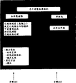
图7至14说明图6中过程的步骤;Figures 7 to 14 illustrate the steps of the process in Figure 6;
图15是按照本发明另一个实施例另一种形式的灯引线框(在单体化之前);Fig. 15 is another form of lamp lead frame (before singulation) according to another embodiment of the present invention;
图16是按照一个实施例部分的灯制作过程;和Figure 16 is a lamp fabrication process according to part of an embodiment; and
图17是按照另一个实施例的灯平面图。Fig. 17 is a plan view of a lamp according to another embodiment.
具体实施方式Detailed ways
相同的参考数字用于指出附图中相同或类似的特征。The same reference numerals are used to designate the same or similar features in the drawings.
首先参照图3A和3B,本发明的优选例涉及灯和制灯方法,它在引线框110上有多个发光结4,引线框110有弯曲的导体10,11和12。发光结4是在各自的插座2中,插座2安装到引线框110,因此在发光结4与弯曲导体10,11,12和13(导体13是供电导体)之间形成电路连接,当灯接通时,通过每个发光结4能够完成电路。导体10,11和12是三维弯曲导体(例如,球面形状),而供电导体13仅是二维弯曲导体(即,弯曲平面)。Referring first to Figures 3A and 3B, the preferred embodiment of the present invention relates to a lamp and method of making a lamp having a plurality of
插座2是与引线框110分开地制成的,而发光结4是在插座2安装到引线框110之前安装在其中。最好是,插座2是利用带状或片状材料整体制成的,然后在发光结4安装到插座2之前或之后与该材料分开。The
插座2(最好是,制成大体凹形杯)的直线阵列1,如图1A,1B和1C所示,最好是利用模压或冲压的常规方法由铜等薄片金属制成。其他形式的插座也是适用的,但是为了简化,以下把所有这种插座称之为杯。为了方便,安装或固定了发光结4的杯2称之为杯组件3。代替直线(一维)阵列,杯可以形成二维薄片阵列。The
优选杯的一个优点是它的形状,可以使每个杯具有光导的功能,用于控制从其中安装的发光结输出光的方向。最好是,每个杯2在图1A所示的平面图上大致是圆形,虽然诸如椭圆或长方形的其他形状也是适用的。优选杯的形状是半径为r的圆形内底面,近似截头圆锥形状的杯壁以角度X(相对于图1B所示的水平面)偏向外半径为R的杯口。在图1B中,参考字符T表示从杯口到杯的圆形内底面之间垂直深度。An advantage of the preferred cups is their shape, which allows each cup to function as a light guide for controlling the direction of light output from a light emitting junction mounted therein. Preferably, each
如图2A所示,杯组件3安装到引线框,使它们的角取向发生位移(基于在安装杯2的区域中有部分球面形状的引线框80)。在图2中,参考字符Z表示这种角位移。As shown in Fig. 2A, the
最好是,杯2的形状以及半径R和r的尺寸,侧(位移)角Z和深度T是由它们各自对从杯射出光图形的影响而确定。最好是,从灯射出的发光强度在总的入射角范围内是线性优化,该角度是从灯射出光束角Y(图2A所示)的2倍。光束所张的立体角2×Y传统上称之为‘半角’。它定义为发光强度超过最大光束值50%的角度范围。这是灯的光学性能中重要的因子,因为它影响该灯的照明效率。Preferably, the shape of the
这些因子R,r,T和角度X的影响,以及引线框的曲率半径C,和引线框的部分球面内每个杯的位移角Z,它们构成确定角Y数值的参数,从而确定组合灯的输出照明图形性质。The influence of these factors R, r, T and angle X, as well as the radius of curvature C of the lead frame, and the displacement angle Z of each cup in the partial sphere of the lead frame, they constitute the parameters determining the value of the angle Y, thereby determining the combined lamp Outputs lighting graphics properties.
这些因子在每种灯设计中是变量,各种灯的设计是相对于优选的半角,灯中安装的杯数目,和杯的相对位置优化这些变量。请参照图15和17,可以得到其他的灯设计例子。These factors are variables in each lamp design, and each lamp design optimizes these variables with respect to the preferred half angle, the number of cups installed in the lamp, and the relative positions of the cups. Please refer to Figures 15 and 17 for other examples of lamp designs.
在制成之后,最好是利用银,银合金或类似材料有选择地电镀杯的阵列。通过形成高反射表面,电镀可以增强每个杯的光学性能,还可以简化所采用的粘接过程(例如,焊接或加银粘合剂)而使杯2限制在引线框的孔6中(图2A所示)。After fabrication, the array of cups is preferably selectively plated with silver, silver alloy or similar material. Electroplating enhances the optical performance of each cup by creating a highly reflective surface, and also simplifies the bonding process employed (e.g., soldering or silvering adhesive) to keep the
在制成和电镀杯线列之后,发光结(模片)4粘接到每个杯的内底面以制成杯组件3。(在整个说明书中,“模片”与“发光结”和“LED”可互换使用)。需要小心地使每个模片与线列对准。最好是,借助于常规方法使阵列中的杯单体化,制作切口以指出极性,冲压(或利用一些其他的方法)标记7到杯2的一侧。在一种优选形式中,标记7是杯上一个外部边缘的截面或扁平。在杯制成之后和电镀之前,可以立刻在杯上制作标记7,为了有助于发光结的极性对准。After the line of cups is fabricated and plated, a light emitting junction (die) 4 is bonded to the inner bottom surface of each cup to make the
在与图2A所示凸形圆顶状不同形式的引线框中,可以制成凹形引线框,如图2B所示。除了引线框支承结构的曲率取向不同以外,按照与图2A和此处描述的附图中所示其他凸形灯实施例的类似方式,可以形成图2B所示的凹形灯实施例。具体地说,参照图6描述的灯制作过程可应用于凹形引线框结构。例如,代替步骤640中制成引线框中央部分的圆顶,可以制成碗形(倒置的圆顶)。这种凹形引线框可以使发光结发射的光更加聚焦,因此,这个实施例更适合于要求聚焦的光分布,而不是均匀的光分布。因此,这个灯实施例的焦距大致等于引线框中央弯曲部分的曲率半径C。在这种情况下,焦点的有效性部分是由曲率半径C的大小确定,同时它也受R,r和T数值的影响。In a different form of lead frame than the convex dome shape shown in FIG. 2A, a concave lead frame can be made as shown in FIG. 2B. The concave lamp embodiment shown in FIG. 2B can be formed in a similar manner to the other convex lamp embodiments shown in FIG. 2A and the figures described herein, except that the curvature orientation of the leadframe support structure is different. In particular, the lamp fabrication process described with reference to FIG. 6 can be applied to a female lead frame structure. For example, instead of forming a dome in the central portion of the lead frame in step 640, a bowl shape (inverted dome) could be formed. This concave lead frame can make the light emitted by the light-emitting junction more focused, so this embodiment is more suitable for a focused light distribution rather than a uniform light distribution. Thus, the focal length of this lamp embodiment is approximately equal to the radius of curvature C of the central curved portion of the lead frame. In this case, the effectiveness of the focal point is determined in part by the size of the radius of curvature C, which is also affected by the values of R, r and T.
通过插入单体杯到引线框110的弯曲引线框导体10,11,12的孔6中,制成配备模片的灯,如图3A所示。在这个实施例中,利用导线连接到第一极性模片的有效部分与导体10,11,12之间,可以连接成对的中间导体14,15,16。此外,利用导线分别连接到第二极性模片的有效部分和共同的供电导体13以及导体11和12,可以连接成对的中间导体17,18,19。这种结构可以控制电流,从而控制发光强度,流动通过导体10,11,12上安装的各组发光结的电流。A die-equipped lamp is made by inserting the cell cup into the hole 6 of the
除了共同的供电导体13以外,图3A中仅展示三个弯曲的引线框导体10,11和12。可以想象,可以采用更多数目弯曲的引线框导体,每个引线框导体支承若干个杯组件。例如,虽然图15表示这样一个引线框实施例,它在三个单独导体113,114,115上分布的各自杯组件内支承18个发光结,但是这种结构可以改变成提供5个单独导体,每个导体支承6个杯组件。还可以设想其他的实施例,虽然没有展示,其中可以支承更大数目的杯组件,例如,50至100个。Apart from the
虽然图3A所示的中间导体17,18,19是成对出现的,但是可以利用单个中间导体,例如,在杯组件3中采用较小的低电流发光结。Although the
图3A和3B所示的实施例特别适合于较大发光结,它比较小发光结可以流过较大的电流,因此需要成对的中间导体以收集和提供电流给模片的激活区。成对的导体还形成第二电流路径,它的作用是减小与仅仅一个中间导体与模片之间电流相关的损耗。The embodiment shown in FIGS. 3A and 3B is particularly suitable for larger light-emitting junctions, which can carry higher currents than smaller light-emitting junctions, thus requiring a pair of intermediate conductors to collect and supply current to the active region of the die. The paired conductors also form a second current path which serves to reduce losses associated with current flow between only one intermediate conductor and the die.
在不同于图3A和3B所示的实施例中,成对的中间导体14,15和16可以连接到杯,而不是连接到弯曲的导体10,11和12。在这个实施例中,每个杯与弯曲导体10,11和12形成电路连接,其中借助于安装在上面的导电材料,例如,焊剂或银胶。这种装置可以使成对的中间导体14,15和16是在杯安装到弯曲导体10,11和12的孔6之前粘接到杯2的内壁。在其他方面,这个实施例类似于图3A和3B所展示和描述的实施例。In an embodiment different from that shown in FIGS. 3A and 3B , the pair of
在另一个实施例中(以下参照图4A和4B所描述的),代替中间导体14,15和16连接到杯的内壁,成对的导体2弯曲6和27分别连接在模片4的阴极和阳极与导电区22和23之间。其他的中间导体连接在弯曲导体10,11和12与导电区22和23之间。In another embodiment (described below with reference to FIGS. 4A and 4B ), instead of the
在另一个实施例中(如图17所示),通过适当地安排中间导体的连接,可以独立地控制流过每个单独发光结的电流。图17表示可以分别和独立控制8个LED的可能安排。在这种安排中,引线框的中央弯曲(球面)部分没有分割成单独的导体,而是安装所有LED的共同导体114。方便的是利用这个共同导体114作为阴极(或负端)。这里展示8个阳极132,每个模片有一个阳极,可以控制阳极流到每个模片的电流。阳极132排列成围绕灯引线框中心部分的幅条形式。方便的是使阴极成为共同导体,因为AlGaInP模片(红和黄)在模片底面上有阴极(它在电路和实际上连接到杯),因此,把它安装到导体上时,它一定是这些模片的阴极,而由于InGaN模片(绿和蓝)有电绝缘的底面,方便的是使这种极性连接标准化。这是与有三组LED引线框的相反极性。这些模片的共同导体是正极,因为芯片的底面(负)可以经设置的导电杯电路连接到引线框的三个弯曲部分中各自的部分。In another embodiment (as shown in FIG. 17 ), by properly arranging the connections of the intermediate conductors, the current flow through each individual light-emitting junction can be independently controlled. Figure 17 shows a possible arrangement where the 8 LEDs can be controlled individually and independently. In this arrangement, the central curved (spherical) portion of the lead frame is not split into individual conductors, but instead houses the
LED发射的光是窄频率或波长带宽,它是可见光谱中的一个特定颜色。有红,黄,绿和蓝光的LED已变得十分普通。若不同颜色的LED安排成图17所示的结构,可以使LED产生的光有不同的颜色,该颜色是构成LED阵列中任何的特征色。通过控制每个LED中的激励电流,就可以控制光输出的强度,它可以使来自LED的光按照不同的比例进行组合,从而产生不同颜色的光。The light emitted by LEDs is a narrow frequency or wavelength bandwidth, which is a specific color in the visible spectrum. LEDs with red, yellow, green and blue light have become very common. If LEDs of different colors are arranged in the structure shown in FIG. 17 , the light generated by the LEDs can have different colors, which are any characteristic colors in the LED array. By controlling the excitation current in each LED, the intensity of the light output can be controlled, which allows the light from the LEDs to be combined in different proportions to produce light of different colors.
例如,按照正确的比例组合红,绿和蓝光可以大致给出白光的外观。类似地,只要使电流通过有相同波长的那些LED,这种灯就可以安排成发射单色光,而通过减小激励第一波长的那些LED和同时增大激励第二波长的一组LED,这种灯就可以改变颜色。在该灯中安装LED模片特征所给出的可能范围内,可以设计合适的控制系统以产生任何的颜色和强度组合。For example, combining red, green, and blue light in the correct proportions can roughly give the appearance of white light. Similarly, such a lamp can be arranged to emit monochromatic light as long as current is passed through those LEDs having the same wavelength, and by reducing the excitation of those LEDs at a first wavelength and simultaneously increasing the excitation of a group of LEDs at a second wavelength, This light can change color. A suitable control system can be designed to produce any combination of colors and intensities within the range of possibilities given by the features of the LED die installed in the lamp.
选取合适的光学材料封装灯,例如,环氧树脂,可以进一步提高LED模片发射光的组合过程。例如,若选取环氧树脂或其他的封装材料,它具有低的光吸收,最小的反向散射,和优越的扩散性质,则可以实现从该灯中几乎均匀的单色发射,并在可见光谱的很大范围内改变颜色。即使一些LED可能安装在灯球面部分的末端,仍然可以实现这个目的,并有大致发散的光束。在另一种结构中,可以选取光透明的低吸收材料进行封装,在此情况下,光组合成单个颜色是不重要的。Selecting a suitable optical material to encapsulate the lamp, for example, epoxy resin, can further improve the combination process of emitting light from the LED die. For example, if an epoxy or other encapsulating material is selected that has low light absorption, minimal backscattering, and superior diffusion properties, it is possible to achieve a nearly uniform monochromatic emission from the lamp, and in the visible spectrum Change colors in a wide range. Even though some LEDs may be mounted at the end of the spherical part of the lamp, this can still be achieved with a roughly diverging beam. In another configuration, light-transparent, low-absorbing materials can be chosen for encapsulation, in which case light combining into a single color is unimportant.
电子工业部门已设计出控制LED阵列和显示器的多种方法。这些方法大致适用于低功率LED,其数量级是每个LED约100毫瓦功率,其中电流控制在20-50毫安的范围内。The electronics industry has devised various methods of controlling LED arrays and displays. These methods are generally suitable for low power LEDs, on the order of about 100 milliwatts per LED, where the current is controlled in the range of 20-50 milliamperes.
面积为1平方毫米的LED模片(模片尺寸为1mm×1mm)需要的激励电流高达350-500毫安倍。电子工业部门的开发预期为2.5平方毫米的LED模片或更大,它需要的激励电流超过1000毫安。一般地说,要求LED控制器具有5瓦/每个LED的功率处理能力,它与当前约100毫瓦/每个LED的处理能力比较,增大50倍。An LED die with an area of 1 square millimeter (the die size is 1mm×1mm) requires an excitation current as high as 350-500 mA. Developments in the electronics industry sector anticipate LED dies of 2.5mm2 or larger, which require excitation currents in excess of 1000mA. Generally speaking, LED controllers are required to have a power handling capability of 5 watts per LED, which is a 50-fold increase compared to the current processing capability of about 100 milliwatts per LED.
本发明包含,但不限于,高达1.26mm×1.26mm的LED模片尺寸,每个LED模片消耗1瓦功率。驱动这种灯的控制电路必须能够控制多个这样的LED。例如,若18个LED安装在灯中,则控制电路必须能够驱动18瓦数量级的输出。The present invention includes, but is not limited to, LED die sizes up to 1.26mm x 1.26mm, each LED die dissipating 1 watt of power. A control circuit that drives such a lamp must be able to control multiple such LEDs. For example, if 18 LEDs are installed in a lamp, the control circuit must be able to drive an output on the order of 18 watts.
在另一个优选实施例中,如图4A和4B所示,在杯凸缘21的上表面,电绝缘层20上有交替的杯32,在绝缘层上叠加导电材料区22和23。这可以使模片24和25的激活区通过连接导线26和27连接到导电区22和23。在粘接模片到杯的过程期间,可以制成这些连接。它大大简化上述的导线连接过程,其中要求粘接设备适应三维阵列。若连接线粘接到杯线列,则简单的常规方法可用于图3A所示的中间连接14和17。这个实施例还可以在许多其他的应用中使用封装的发光结。常用的‘元件置放’机可用于自动安装杯和进行连接。In another preferred embodiment, as shown in Figures 4A and 4B, on the upper surface of the cup flange 21, there are alternating
导电区22和23最好制成绝缘层上的一个薄层,它加到每个杯的边缘。绝缘材料可以是环氧树脂或一些其他复合物,它们对杯表面有良好的粘附性并有薄层形式的良好电绝缘。利用金属沉积或其他合适的方法制成导电区。这种方法用于制作印刷电路,特别是金属芯印刷电路,它们通常制成在铝的金属基片上。The
杯组件3或封装(即,安装发光结的杯)大大优于其他表面封装中的发光结。可以极大地克服常规封装中散热差的限制。杯封装可以容易地直接安装到‘金属芯印刷电路板’(MCPCB)的预制切口中,因此可应用于灯照明以外的领域。可以建立几乎理想的热导路径,它是从热源(模片)通过杯材料和直接地进入MCPCB的高散热芯。The
模片尺寸的约束和模片可以耗散功率的实际限制控制当前这些装置中的光质量。提供一种有效和方便地耗散模片中热量的方法,可以有效地去除对成功采用的模片尺寸的实际限制。因此,可以简单和廉价地制作这样的杯,它设计成适合于消耗几瓦功率的模片,且杯产生的光大致正比于输入功率。Die size constraints and practical limits to the power that a die can dissipate control the quality of light in these devices today. Providing an efficient and convenient means of dissipating heat from the die effectively removes practical limitations on the size of the die that can be successfully employed. Thus, cups can be made easily and cheaply, designed for dies that dissipate a few watts of power, and the light produced by the cup is approximately proportional to the input power.
以下的表1给出可用于本发明实施例的较大LED模片例子。在市场上有各种较小的LED模片,专业人员熟知这些合适的模片。Table 1 below gives examples of larger LED dies that may be used in embodiments of the present invention. Various smaller LED dies are available on the market and suitable dies are well known to professionals.
表1
现在参照图6,图6表示按照本发明实施例可以制作灯的流程图。优选的制灯过程涉及分开地制作其中已安装发光结的杯,以及一旦引线框制造到某个阶段(即,步骤640之后),安装杯组件到引线框。一旦杯粘接到引线框,在步骤665,对它们进行处理以制成灯。Referring now to FIG. 6, there is shown a flow diagram by which a lamp may be fabricated in accordance with an embodiment of the present invention. A preferred lamp making process involves separately making the cup into which the light-emitting junction is mounted, and once the leadframe is manufactured to a certain stage (ie, after step 640), mounting the cup assembly to the leadframe. Once the cups are bonded to the leadframe, at step 665, they are processed to make lamps.
在步骤605,利用冲压工具,由铜板或其他合适薄片或带状可变形导电材料制作杯,从薄板或薄片冲压每个杯以制成图1A至1C所示的插座。步骤605包括在每个杯上制成标记7。一旦被冲压的材料单体化,在步骤610,利用银,铝或其他导电材料电镀杯以获得约4至8微米的电镀厚度,例如,利用滚筒镀,精密电镀或汽相沉积。在电镀之后,在步骤615,模片(图6中称之为芯片)粘接到杯的内侧底面,最好是利用银胶,使发光结面向外远离底面。一旦发光结在步骤615粘接到杯,如此制成的杯组件可以封装成直线带状或二维薄片,然后把它馈送到机器人元件置放机,例如,表面安装技术中使用的装置。At step 605, cups are fabricated from copper plates or other suitable sheets or strips of deformable conductive material using a stamping tool, and each cup is punched from the sheet or sheet to form the socket shown in Figures 1A to 1C. Step 605 includes making
独立于杯的制作,在步骤620,对引线框的基本形状进行机械加工,开始处理引线框。机械加工可以是蚀刻或机械冲压,最好是,引线框是由铜或铜合金薄片材料制成,其厚度约为400微米。引线框材料的厚度最好选取为有最佳的热传导,使多余的热量离开杯组件。例如,若较大的模片安装在杯组件中,则它产生比使用较小模片更多的热量。增大引线框的厚度有助于使这种热量离开灯。在球面变形和分开成单独导体之前,步骤620中制成的引线框基本形状在铜片材料周围支承框架内包含导体10,11,12和13。在步骤625,最好利用银或铝,对每个引线框的中央导电部分(它变成导体10,11,12和13)电镀到约4至8微米的厚度。至少电镀放置杯并与其电接触的引线框中央部分,但为了经济或方便,也可以电镀引线框的整个上表面。一旦完成电镀,在步骤630,在引线框的中央(电镀)部分打孔。在引线框的中央部分形成球面形状之后,这些孔形成图2所示放置杯的孔6。其次,在步骤635,把导体10,11和12进行分割(最好是,在步骤620已分割出导体13),为的是使引线框中央部分中一些孔互相隔开。这种分割最好是利用平滑和精密切割工具完成的,因此,就不需要对分割期间在导体之间形成的边缘进行抛光的附加处理。Independently of the fabrication of the cup, at step 620, the basic shape of the leadframe is machined to begin processing the leadframe. Machining can be etching or mechanical stamping, and preferably, the lead frame is made of copper or copper alloy thin sheet material with a thickness of about 400 microns. The thickness of the leadframe material is preferably selected for optimum heat conduction, allowing excess heat to leave the cup assembly. For example, if a larger die is installed in the cup assembly, it generates more heat than if a smaller die were used. Increasing the thickness of the leadframe helps keep this heat away from the lamp. The basic shape of the lead frame produced in step 620 contains the
在引线框的中央导电部分,按照所要求的孔组合完成分割。因此,这种组合取决于步骤630中该部分形成的孔数目。在一个优选实施例中,如图15所示,在引线框中可以制成不同数目的孔,用于放置其中有发光结的杯。图15所示的另一个实施例在引线框110的中央部分有制成的18个孔120,这些孔在导体113,114和115上分成三个组,每组有6个孔。步骤635的分割还必须考虑到引线框材料在随后步骤640制作圆顶时发生的变形。例如,导体11中形成的孔有略微变形的趋势(伸长后有些像椭圆),它是沿着球面圆顶制作期间电镀引线框材料变形的方向。因此,可以在步骤630和635完成孔的形成和分割,为的是补偿圆顶制成期间材料的变形,例如,在导体11上形成扁平的椭圆形状,因此,在圆顶制作步骤时伸长为较圆的形状。In the central conductive part of the lead frame, the separation is done according to the required combination of holes. Therefore, this combination depends on the number of holes formed in the part in step 630 . In a preferred embodiment, as shown in FIG. 15, different numbers of holes can be made in the lead frame for placing cups with light-emitting junctions therein. Another embodiment shown in FIG. 15 has 18
最好是,圆顶制作步骤640是利用某种冲压工具完成的,为的是在引线框的中央部分形成大致的部分球面形状。Preferably, the dome forming step 640 is performed using a stamping tool of some kind to form a generally part-spherical shape in the central portion of the lead frame.
在步骤645,步骤605至615制成的杯组件3粘接到圆顶制作步骤640之后的引线框。一旦杯组件放置在孔6之后,例如,利用精密的机器人装置,这种粘接最好是通过焊接,熔接或利用导电粘合剂。在杯组件放置到孔中并固定之后,在步骤650完成导线连接,从而使杯中的发光结电路连接到导体10,11,12和13,如以上所描述的。为了完成这种导线连接,利用已知的热/超声焊接技术,最好是使用金导线,导线的直径为25-50微米。使用不同导线材料和导线直径的其他形式连接技术对于专业人员是众所周知的,而且还可以交替地使用。In step 645 , the
在导线连接之后,在步骤655,可以任选地把磷加到各个发光结的顶部。这是通过均匀地混合磷粉到环氧树脂并以环氧树脂滴形式分配到每个发光结的顶部发光面。在步骤660,光透明环氧树脂或热塑性塑料加到引线框中央部分给予封闭。在步骤655,若磷粉没有沉积到各个发光结,则在步骤660,磷粉可以与封闭引线框中央部分的环氧树脂混合。为了加环氧树脂或热塑性塑料,引线框被倒置并放置在互补的部分球面形状的模具中。一旦环氧树脂或热塑性塑料有固化或凝结,则在步骤665,对引线框进行处理,使引线框之间互相分离,包括给导体10,11,12和13打孔,这些导体在加环氧树脂之前没有那些把引线框固定在一起的部分。还是在这个步骤,去除连接导体10,11和12的金属薄片(从附图中可以看出),例如,通过打孔使那些导体之间互相绝缘。After wire connection, at step 655, phosphorous can optionally be added to the top of each light emitting junction. This is done by evenly mixing the phosphor powder into the epoxy and dispensing drops of epoxy onto the top emitting surface of each light emitting junction. At step 660, light clear epoxy or thermoplastic is applied to the central portion of the lead frame to impart closure. At step 655, if the phosphor powder is not deposited on the individual light emitting junctions, then at step 660, the phosphor powder may be mixed with epoxy enclosing the central portion of the lead frame. To add epoxy or thermoplastic, the leadframe is inverted and placed in a complementary part-spherical shaped mold. Once the epoxy or thermoplastic has cured or congealed, then at step 665, the leadframes are processed to separate the leadframes from each other, including perforating the
图7至14说明上述过程的步骤,与以下表2的结合,用于描述按照优选实施例的制作过程。以下的表2总结一些上述的处理步骤,优选方法和这些步骤中使用的材料。Figures 7 to 14 illustrate the steps of the above process, which, in combination with Table 2 below, are used to describe the fabrication process in accordance with the preferred embodiment. Table 2 below summarizes some of the aforementioned processing steps, preferred methods and materials used in these steps.
表2
图15表示另一种形式引线框110,它在其中央部分有较多数目的孔120。导体113,114和115中的每个导体支承6个杯组件,并具有这样的安排,当灯工作时,它可以提供来自发光结均匀的光分布。导体113,114和115上孔组的精确配置和位置可以根据需要而变化,以便获得所需的光输出图形。孔120的数目和定位也可以变化,它取决于实际的制作要求。Fig. 15 shows another form of
图16表示部分的灯制作过程,它大致对应于图6中的步骤645,其中杯组件放置在引线框110的孔6或120中。按顺序处理托架119上的引线框110,因此,杯组件3可以放置在切口120(孔6)中。托架119的结构可以与引线框的部分球面和参考标记对准。这个对准部分可以是升起的凸面,它与凸形引线框的凹面底侧互补,或者,这个对准部分可以是凹形切口,它与凹形引线框的凸面底侧互补。利用托架上交替的轮廓,可以构造图2A和图2B所示的凸形和凹形灯轮廓。托架119可以绕转轴121转动,它形成绕X轴的转动和绕Y轴的转动。按照这种方式,引线框110可以定位在固定台(未画出),并相对于固定台作绕X轴或Y轴的转动,为的是便于放置杯组件3到切口中。或者,若我们有合适的机器人机构,则托架119可以安装定位,考虑到引线框中央部分的部分球面形状,机器人定位机构可以放置杯组件3到各自的切口。在这个实施例中,沿着引线框110的外边缘设置参考标记,便于机器人机构作位置校准。FIG. 16 shows a part of the lamp fabrication process which roughly corresponds to step 645 in FIG. The
在不偏离本发明精神和范围的条件下,专业人员可以对以上描述的这些实施例作某些改进和增强。Certain modifications and enhancements to the above-described embodiments may be made by those skilled in the art without departing from the spirit and scope of the invention.
Claims (50)
Applications Claiming Priority (6)
| Application Number | Priority Date | Filing Date | Title |
|---|---|---|---|
| AUPS2979 | 2002-06-14 | ||
| AUPS2979A AUPS297902A0 (en) | 2002-06-14 | 2002-06-14 | A method of producing a lamp |
| AU2002950814 | 2002-08-14 | ||
| AU2002950814A AU2002950814A0 (en) | 2002-08-14 | 2002-08-14 | A lamp and a method of producing a lamp |
| AU2003901114 | 2003-03-12 | ||
| AU2003901114A AU2003901114A0 (en) | 2003-03-12 | 2003-03-12 | A lamp and a method of producing a lamp |
Related Child Applications (1)
| Application Number | Title | Priority Date | Filing Date |
|---|---|---|---|
| CNA2008100919133A Division CN101320699A (en) | 2002-06-14 | 2003-06-11 | LED packaging method and packaged LED |
Publications (1)
| Publication Number | Publication Date |
|---|---|
| CN1663044A true CN1663044A (en) | 2005-08-31 |
Family
ID=29740321
Family Applications (1)
| Application Number | Title | Priority Date | Filing Date |
|---|---|---|---|
| CN038138530A Pending CN1663044A (en) | 2002-06-14 | 2003-06-11 | Lamps and methods of making them |
Country Status (10)
| Country | Link |
|---|---|
| US (2) | US7704762B2 (en) |
| EP (2) | EP1552560A4 (en) |
| JP (2) | JP4620458B2 (en) |
| KR (1) | KR20080064904A (en) |
| CN (1) | CN1663044A (en) |
| AU (1) | AU2003233248B2 (en) |
| CA (2) | CA2488904A1 (en) |
| NZ (1) | NZ531587A (en) |
| TW (1) | TWI297219B (en) |
| WO (1) | WO2003107423A1 (en) |
Cited By (3)
| Publication number | Priority date | Publication date | Assignee | Title |
|---|---|---|---|---|
| CN102116455A (en) * | 2010-12-11 | 2011-07-06 | 郭小华 | Efficient light-emitting LED (Light Emitting Diode) packaging surface |
| CN106461169A (en) * | 2014-05-30 | 2017-02-22 | 皇家飞利浦有限公司 | LEDs mounted on curved lead frame |
| CN110808242A (en) * | 2019-11-20 | 2020-02-18 | 侯立东 | LED lamp string and manufacturing method thereof |
Families Citing this family (31)
| Publication number | Priority date | Publication date | Assignee | Title |
|---|---|---|---|---|
| US7320632B2 (en) | 2000-06-15 | 2008-01-22 | Lednium Pty Limited | Method of producing a lamp |
| AUPQ818100A0 (en) * | 2000-06-15 | 2000-07-06 | Arlec Australia Limited | Led lamp |
| EP1552560A4 (en) * | 2002-06-14 | 2006-10-25 | Lednium Pty Ltd | LAMP AND METHOD FOR PRODUCING THE SAME |
| CA2518625A1 (en) * | 2003-03-12 | 2004-09-23 | Lednium Pty. Ltd. | A lamp and a process for producing a lamp |
| EP1496551B1 (en) * | 2003-07-09 | 2013-08-21 | Nichia Corporation | Light emitting diode, method of manufacturing the same and lighting equipment incorporating the same |
| US7575030B2 (en) * | 2003-12-10 | 2009-08-18 | Hutchinson | Runflat device for a motor vehicle, and a mounted assembly incorporating it |
| TWI413445B (en) * | 2004-06-03 | 2013-10-21 | Koninkl Philips Electronics Nv | Lighting circuit |
| TW200629596A (en) | 2004-09-16 | 2006-08-16 | Hitachi Aic Inc | Reflector for led and led device |
| EP1825524A4 (en) * | 2004-12-16 | 2010-06-16 | Seoul Semiconductor Co Ltd | CONNECTION GRID COMPRISING A THERMAL DISSIPATOR SUPPORT RING, METHOD FOR MANUFACTURING LIGHT-EMITTING DIODE HOUSING USING THE SAME, AND LIGHT-EMITTING DIODE HOUSING MADE THEREBY |
| US20060231848A1 (en) * | 2005-04-14 | 2006-10-19 | Chien-Kun Fu | Light emitting diode package for enhancing light extraction |
| KR20070045462A (en) | 2005-10-27 | 2007-05-02 | 엘지이노텍 주식회사 | Light emitting diode package |
| JP2007150080A (en) * | 2005-11-29 | 2007-06-14 | Mitsubishi Rayon Co Ltd | Linear light equipment |
| US7829899B2 (en) | 2006-05-03 | 2010-11-09 | Cree, Inc. | Multi-element LED lamp package |
| US7960819B2 (en) * | 2006-07-13 | 2011-06-14 | Cree, Inc. | Leadframe-based packages for solid state emitting devices |
| US8044418B2 (en) | 2006-07-13 | 2011-10-25 | Cree, Inc. | Leadframe-based packages for solid state light emitting devices |
| JP2008198807A (en) * | 2007-02-14 | 2008-08-28 | Nichia Corp | Semiconductor device |
| US7918596B2 (en) | 2007-04-20 | 2011-04-05 | Federal Signal Corporation | Warning light |
| NZ584533A (en) | 2007-10-25 | 2012-05-25 | Lsi Industries Inc | Reflector for positioning over an array of leds or other light sources |
| KR100998233B1 (en) | 2007-12-03 | 2010-12-07 | 서울반도체 주식회사 | Slim LED Package |
| KR20110080165A (en) * | 2008-10-17 | 2011-07-12 | 루미너스 디바이시즈, 아이엔씨. | Remote lighting assembly and method |
| KR100928159B1 (en) * | 2008-12-24 | 2009-11-23 | 한성엘컴텍 주식회사 | Light source module and lighting device using the same |
| KR200454746Y1 (en) * | 2009-06-26 | 2011-07-22 | 안대주 | Lighting device including a light emitting element |
| JP5612355B2 (en) * | 2009-07-15 | 2014-10-22 | 株式会社Kanzacc | Plating structure and method of manufacturing electrical material |
| US7932532B2 (en) * | 2009-08-04 | 2011-04-26 | Cree, Inc. | Solid state lighting device with improved heatsink |
| KR101078642B1 (en) | 2009-08-25 | 2011-11-01 | 태산엘시디 주식회사 | Light emitting diode module for back light |
| JP5390566B2 (en) * | 2011-07-14 | 2014-01-15 | シャープ株式会社 | LIGHT EMITTING DEVICE PRODUCTION DEVICE AND ITS PRODUCTION METHOD, LIGHT EMITTING MODULE PRODUCTION DEVICE AND ITS PRODUCTION METHOD, LIGHT EMITTING MODULE, LIGHT SOURCE DEVICE, AND LIQUID CRYSTAL DISPLAY DEVICE |
| US9140441B2 (en) | 2012-08-15 | 2015-09-22 | Cree, Inc. | LED downlight |
| US9797565B2 (en) | 2012-10-31 | 2017-10-24 | Thomas & Betts International Llc | LED engine for emergency lighting |
| TWI474432B (en) * | 2012-11-15 | 2015-02-21 | Lextar Electronics Corp | Die grain positioning device, grain positioning system with grain positioning device and grain positioning method of light emitting diode display panel |
| CN107940270A (en) * | 2017-11-22 | 2018-04-20 | 江门市晶典照明有限公司 | A kind of LED light strip covers canal table |
| KR102653015B1 (en) | 2018-07-18 | 2024-03-29 | 삼성전자주식회사 | Light emitting device, head lamp for vehicle, and vehicle comprising the same |
Family Cites Families (114)
| Publication number | Priority date | Publication date | Assignee | Title |
|---|---|---|---|---|
| US3581162A (en) | 1969-07-01 | 1971-05-25 | Rca Corp | Optical semiconductor device |
| JPS5026433B1 (en) | 1970-12-21 | 1975-09-01 | ||
| US3821775A (en) * | 1971-09-23 | 1974-06-28 | Spectronics Inc | Edge emission gaas light emitter structure |
| JPS48102585A (en) * | 1972-04-04 | 1973-12-22 | ||
| JPS5127988B2 (en) | 1972-09-05 | 1976-08-16 | ||
| US3942185A (en) | 1972-12-13 | 1976-03-02 | U.S. Philips Corporation | Polychromatic electroluminescent device |
| FR2248663B1 (en) | 1972-12-13 | 1978-08-11 | Radiotechnique Compelec | |
| JPS5310862Y2 (en) | 1972-12-28 | 1978-03-23 | ||
| US3886681A (en) | 1973-08-29 | 1975-06-03 | Mattel Inc | Control member for toy airplane |
| GB1522145A (en) | 1974-11-06 | 1978-08-23 | Marconi Co Ltd | Light emissive diode displays |
| US4054814A (en) | 1975-10-31 | 1977-10-18 | Western Electric Company, Inc. | Electroluminescent display and method of making |
| US4173035A (en) | 1977-12-01 | 1979-10-30 | Media Masters, Inc. | Tape strip for effecting moving light display |
| US4255688A (en) | 1977-12-15 | 1981-03-10 | Tokyo Shibaura Denki Kabushiki Kaisha | Light emitter mounted on reflector formed on end of lead |
| US4271408A (en) | 1978-10-17 | 1981-06-02 | Stanley Electric Co., Ltd. | Colored-light emitting display |
| JPS57156442A (en) | 1981-03-23 | 1982-09-27 | Kuraray Co Ltd | Preparation of methyl lactate |
| US4467193A (en) | 1981-09-14 | 1984-08-21 | Carroll Manufacturing Corporation | Parabolic light emitter and detector unit |
| DE3148843C2 (en) | 1981-12-10 | 1986-01-02 | Telefunken electronic GmbH, 7100 Heilbronn | Multiple light emitting diode arrangement |
| US4473834A (en) | 1982-04-19 | 1984-09-25 | Rockwell International Corporation | Light emitting transistor array |
| JPS5974687A (en) | 1982-10-21 | 1984-04-27 | Idec Izumi Corp | Light emitting diode lamp |
| FR2554606B1 (en) | 1983-11-04 | 1987-04-10 | Thomson Csf | OPTICAL DEVICE FOR CONCENTRATION OF LIGHT RADIATION EMITTED BY A LIGHT EMITTING DIODE, AND LIGHT EMITTING DIODE COMPRISING SUCH A DEVICE |
| JPS6132483A (en) | 1984-07-24 | 1986-02-15 | Kimura Denki Kk | Spherical luminous body using led |
| DE3438154C2 (en) | 1984-10-18 | 1994-09-15 | Teves Gmbh Alfred | Rear lights for motor vehicles |
| JPS61141165A (en) * | 1984-12-14 | 1986-06-28 | Toshiba Corp | Lead frame for semiconductor device |
| FR2588109B1 (en) | 1985-10-02 | 1987-12-11 | Valancogne Pierre | LIGHT SIGNALING DEVICE |
| DE3685749T2 (en) | 1985-10-29 | 1993-01-21 | William R Hopper | KEY-SENSITIVE INDICATOR LIGHT. |
| JPH0680841B2 (en) * | 1986-04-07 | 1994-10-12 | 株式会社小糸製作所 | Lighting equipment |
| JPH0326536Y2 (en) | 1986-10-01 | 1991-06-07 | ||
| US4914731A (en) | 1987-08-12 | 1990-04-03 | Chen Shen Yuan | Quickly formed light emitting diode display and a method for forming the same |
| US4935665A (en) * | 1987-12-24 | 1990-06-19 | Mitsubishi Cable Industries Ltd. | Light emitting diode lamp |
| DE3827083A1 (en) | 1988-08-10 | 1990-02-15 | Telefunken Electronic Gmbh | AREA SPOTLIGHT |
| DE3835942A1 (en) | 1988-10-21 | 1990-04-26 | Telefunken Electronic Gmbh | AREA SPOTLIGHT |
| US4893223A (en) | 1989-01-10 | 1990-01-09 | Northern Telecom Limited | Illumination devices for inspection systems |
| US5055892A (en) | 1989-08-29 | 1991-10-08 | Hewlett-Packard Company | High efficiency lamp or light accepter |
| DE4107526C2 (en) | 1990-03-26 | 1996-04-11 | Siemens Ag | Luminescent diode device with protective device for limiting the forward current when AC voltage is present |
| US5083192A (en) * | 1990-04-30 | 1992-01-21 | Kulicke And Soffa Industries, Inc. | Cluster mount for high intensity leds |
| JP2535651B2 (en) | 1990-07-24 | 1996-09-18 | 株式会社東芝 | Semiconductor device |
| KR950003955B1 (en) | 1990-09-07 | 1995-04-21 | 가부시키가이샤도시바 | Led lamp |
| US5119174A (en) | 1990-10-26 | 1992-06-02 | Chen Der Jong | Light emitting diode display with PCB base |
| DE4124413A1 (en) | 1991-07-23 | 1993-01-28 | Bernd Herzhoff | Subminiature, semiconductor, power solid state laser - is optically energised by number of LED chips with radiation impinging on jacket of laser-active crystal |
| FR2680862B1 (en) | 1991-09-02 | 1997-08-08 | Valeo Vision | SIGNAL LIGHT WITH LIGHT EMITTING ELEMENTS, PARTICULARLY FOR MOTOR VEHICLE. |
| FR2680859B1 (en) | 1991-09-02 | 1993-10-29 | Valeo Vision | OPTICAL COLLIMATION ELEMENT AND ITS ASSOCIATED SUPPORT ELEMENT, IN PARTICULAR FOR A MOTOR VEHICLE SIGNALING LIGHT. |
| JP3096824B2 (en) | 1992-04-17 | 2000-10-10 | ローム株式会社 | LED manufacturing frame and LED manufacturing method using the same |
| CA2152356C (en) | 1992-12-24 | 2005-05-10 | Robert Michael | Pixel, video display screen and power delivery |
| JP3258738B2 (en) * | 1993-01-22 | 2002-02-18 | 三洋電機株式会社 | Light emitting diode display |
| US5534718A (en) * | 1993-04-12 | 1996-07-09 | Hsi-Huang Lin | LED package structure of LED display |
| FR2707222B1 (en) | 1993-07-07 | 1995-09-29 | Valeo Vision | Improved signaling light with light-emitting diodes. |
| US5404282A (en) | 1993-09-17 | 1995-04-04 | Hewlett-Packard Company | Multiple light emitting diode module |
| DE9316106U1 (en) | 1993-10-21 | 1994-02-03 | Chang, Fa-Sheng, Hsintien, Taipeh | LED construction |
| US5561346A (en) | 1994-08-10 | 1996-10-01 | Byrne; David J. | LED lamp construction |
| US5709453A (en) | 1994-08-16 | 1998-01-20 | Krent; Edward D. | Vehicle lighting having remote light source |
| JP3033883B2 (en) | 1994-11-30 | 2000-04-17 | ローム株式会社 | Light emitting display |
| US5519596A (en) | 1995-05-16 | 1996-05-21 | Hewlett-Packard Company | Moldable nesting frame for light emitting diode array |
| US5515253A (en) | 1995-05-30 | 1996-05-07 | Sjobom; Fritz C. | L.E.D. light assembly |
| DE19549818B4 (en) * | 1995-09-29 | 2010-03-18 | Osram Opto Semiconductors Gmbh | Optoelectronic semiconductor device |
| GB9605314D0 (en) | 1996-03-13 | 1996-05-15 | Toher C H | Non-filament lights |
| US6034712A (en) * | 1996-06-26 | 2000-03-07 | Brother Kogyo Kabushiki Kaisha | Exposure apparatus and image forming machine including it |
| TW383508B (en) | 1996-07-29 | 2000-03-01 | Nichia Kagaku Kogyo Kk | Light emitting device and display |
| JP3752760B2 (en) | 1997-01-14 | 2006-03-08 | 豊田合成株式会社 | Light emitting diode device |
| JPH10242523A (en) | 1997-02-28 | 1998-09-11 | Kouha:Kk | Light emitting diode display device and image display device using the same |
| JP3948789B2 (en) * | 1997-07-02 | 2007-07-25 | シチズン電子株式会社 | Infrared data communication module |
| US5962971A (en) | 1997-08-29 | 1999-10-05 | Chen; Hsing | LED structure with ultraviolet-light emission chip and multilayered resins to generate various colored lights |
| TW408497B (en) | 1997-11-25 | 2000-10-11 | Matsushita Electric Works Ltd | LED illuminating apparatus |
| JPH11163412A (en) | 1997-11-25 | 1999-06-18 | Matsushita Electric Works Ltd | Led illuminator |
| JP3454123B2 (en) | 1997-11-25 | 2003-10-06 | 松下電工株式会社 | LED lighting module |
| JP3505985B2 (en) | 1997-11-25 | 2004-03-15 | 松下電工株式会社 | LED lighting module |
| JP3618534B2 (en) | 1997-11-28 | 2005-02-09 | 同和鉱業株式会社 | Optical communication lamp device and manufacturing method thereof |
| JPH11177144A (en) | 1997-12-15 | 1999-07-02 | Iwasaki Electric Co Ltd | LED array |
| US6412971B1 (en) | 1998-01-02 | 2002-07-02 | General Electric Company | Light source including an array of light emitting semiconductor devices and control method |
| US6068383A (en) | 1998-03-02 | 2000-05-30 | Robertson; Roger | Phosphorous fluorescent light assembly excited by light emitting diodes |
| JP3114805B2 (en) | 1998-04-15 | 2000-12-04 | 日亜化学工業株式会社 | Planar light source, display backlight using the same, and illuminated operation switch |
| FR2779508B1 (en) | 1998-06-03 | 2000-08-25 | Valeo Vision | SIGNAL LIGHT WITH GALBED WINDOW, ESPECIALLY A COMPLEMENTARY STOP LIGHT, FOR A MOTOR VEHICLE |
| US5959316A (en) | 1998-09-01 | 1999-09-28 | Hewlett-Packard Company | Multiple encapsulation of phosphor-LED devices |
| US6337953B1 (en) * | 1998-11-16 | 2002-01-08 | Konica Corporation | Strobe device of lens-fitted film unit and production method of the strobe device |
| JP3366586B2 (en) | 1998-12-28 | 2003-01-14 | 日亜化学工業株式会社 | Light emitting diode |
| JP3920486B2 (en) | 1999-02-23 | 2007-05-30 | 株式会社小糸製作所 | Vehicle lighting |
| JP3447604B2 (en) | 1999-02-25 | 2003-09-16 | 株式会社シチズン電子 | Surface mount type light emitting diode and method of manufacturing the same |
| US6521916B2 (en) | 1999-03-15 | 2003-02-18 | Gentex Corporation | Radiation emitter device having an encapsulant with different zones of thermal conductivity |
| DE19922176C2 (en) | 1999-05-12 | 2001-11-15 | Osram Opto Semiconductors Gmbh | Surface-mounted LED multiple arrangement and its use in a lighting device |
| JP2001007406A (en) * | 1999-06-25 | 2001-01-12 | Iwasaki Electric Co Ltd | LED array |
| EP2131404A3 (en) | 1999-07-26 | 2010-01-06 | Labosphere Institute | Bulk-shaped lens, light-emitting unit, lighting equipment and optical information system |
| US6367949B1 (en) * | 1999-08-04 | 2002-04-09 | 911 Emergency Products, Inc. | Par 36 LED utility lamp |
| US7294364B2 (en) * | 1999-09-24 | 2007-11-13 | Cao Group, Inc. | Method for curing composite materials |
| US6971875B2 (en) * | 1999-09-24 | 2005-12-06 | Cao Group, Inc. | Dental curing light |
| US20040120146A1 (en) * | 2002-12-20 | 2004-06-24 | Cao Group, Inc | Forensic light kit using semiconductor light source |
| GB2356037B (en) | 1999-11-03 | 2004-03-31 | Page Aerospace Ltd | A semiconductor light source |
| JP3696021B2 (en) * | 2000-01-20 | 2005-09-14 | 三洋電機株式会社 | Light irradiation device |
| US6318886B1 (en) * | 2000-02-11 | 2001-11-20 | Whelen Engineering Company | High flux led assembly |
| US6409938B1 (en) | 2000-03-27 | 2002-06-25 | The General Electric Company | Aluminum fluoride flux synthesis method for producing cerium doped YAG |
| GB2361581A (en) | 2000-04-20 | 2001-10-24 | Lite On Electronics Inc | A light emitting diode device |
| DE10025563B4 (en) * | 2000-05-24 | 2005-12-01 | Osram Opto Semiconductors Gmbh | Module for the arrangement of electric light-emitting elements, which can be integrated into a luminaire housing, and method for producing such a module |
| AUPQ818100A0 (en) * | 2000-06-15 | 2000-07-06 | Arlec Australia Limited | Led lamp |
| US7320632B2 (en) | 2000-06-15 | 2008-01-22 | Lednium Pty Limited | Method of producing a lamp |
| AUPR570501A0 (en) * | 2001-06-15 | 2001-07-12 | Q1 (Pacific) Limited | Led lamp |
| JP4432275B2 (en) * | 2000-07-13 | 2010-03-17 | パナソニック電工株式会社 | Light source device |
| DE20013605U1 (en) | 2000-07-28 | 2000-12-28 | Opto-System GmbH, 12555 Berlin | Elongated light source |
| US6552368B2 (en) * | 2000-09-29 | 2003-04-22 | Omron Corporation | Light emission device |
| TW521409B (en) * | 2000-10-06 | 2003-02-21 | Shing Chen | Package of LED |
| DE10051159C2 (en) * | 2000-10-16 | 2002-09-19 | Osram Opto Semiconductors Gmbh | LED module, e.g. White light source |
| JP2001228812A (en) * | 2000-12-22 | 2001-08-24 | Sharp Corp | Display apparatus |
| EP1244152A3 (en) | 2001-01-26 | 2008-12-03 | Toyoda Gosei Co., Ltd. | Reflective light emitting diode, reflective optical device and its manufacturing method |
| JP3920031B2 (en) | 2001-02-20 | 2007-05-30 | 株式会社小糸製作所 | Vehicle lighting |
| US6541800B2 (en) * | 2001-02-22 | 2003-04-01 | Weldon Technologies, Inc. | High power LED |
| ATE425556T1 (en) * | 2001-04-12 | 2009-03-15 | Matsushita Electric Works Ltd | LIGHT SOURCE COMPONENT WITH LED AND METHOD FOR PRODUCING IT |
| JP4905751B2 (en) | 2001-05-17 | 2012-03-28 | 株式会社吉田製作所 | Dental light irradiator |
| DE20110289U1 (en) | 2001-06-21 | 2001-08-23 | Büchner, Thomas, 86465 Welden | Lighting device |
| JP4129570B2 (en) * | 2001-07-18 | 2008-08-06 | ラボ・スフィア株式会社 | Light emitting diode lighting device |
| ATE356532T1 (en) * | 2001-09-13 | 2007-03-15 | Lucea Ag | LED LIGHT PANEL AND CIRCUIT BOARD |
| WO2003030274A1 (en) * | 2001-09-27 | 2003-04-10 | Nichia Corporation | Light-emitting device and its manufacturing method |
| US6599000B2 (en) | 2001-10-15 | 2003-07-29 | Steven T. Nolan | Interior lamp for producing white light using bright white LEDs |
| JP4009097B2 (en) | 2001-12-07 | 2007-11-14 | 日立電線株式会社 | LIGHT EMITTING DEVICE, ITS MANUFACTURING METHOD, AND LEAD FRAME USED FOR MANUFACTURING LIGHT EMITTING DEVICE |
| EP1552560A4 (en) * | 2002-06-14 | 2006-10-25 | Lednium Pty Ltd | LAMP AND METHOD FOR PRODUCING THE SAME |
| WO2004053385A2 (en) * | 2002-12-11 | 2004-06-24 | Charles Bolta | Light emitting diode (l.e.d.) lighting fixtures with emergency back-up and scotopic enhancement |
| US20040120151A1 (en) * | 2002-12-20 | 2004-06-24 | Cao Group, Inc. | Forensic light using semiconductor light source |
| US6903380B2 (en) * | 2003-04-11 | 2005-06-07 | Weldon Technologies, Inc. | High power light emitting diode |
-
2003
- 2003-06-11 EP EP03727013A patent/EP1552560A4/en not_active Withdrawn
- 2003-06-11 AU AU2003233248A patent/AU2003233248B2/en not_active Ceased
- 2003-06-11 CN CN038138530A patent/CN1663044A/en active Pending
- 2003-06-11 CA CA002488904A patent/CA2488904A1/en not_active Abandoned
- 2003-06-11 JP JP2004514135A patent/JP4620458B2/en not_active Expired - Lifetime
- 2003-06-11 CA CA002634288A patent/CA2634288A1/en not_active Abandoned
- 2003-06-11 NZ NZ531587A patent/NZ531587A/en not_active IP Right Cessation
- 2003-06-11 WO PCT/AU2003/000724 patent/WO2003107423A1/en active Application Filing
- 2003-06-11 EP EP08005654A patent/EP1939939A3/en not_active Withdrawn
- 2003-06-11 US US10/487,040 patent/US7704762B2/en active Active
- 2003-06-11 KR KR1020087013930A patent/KR20080064904A/en not_active Application Discontinuation
- 2003-06-12 TW TW092115951A patent/TWI297219B/en not_active IP Right Cessation
-
2008
- 2008-04-18 JP JP2008109234A patent/JP2008205501A/en active Pending
-
2010
- 2010-03-11 US US12/722,487 patent/US20100163913A1/en not_active Abandoned
Cited By (4)
| Publication number | Priority date | Publication date | Assignee | Title |
|---|---|---|---|---|
| CN102116455A (en) * | 2010-12-11 | 2011-07-06 | 郭小华 | Efficient light-emitting LED (Light Emitting Diode) packaging surface |
| CN106461169A (en) * | 2014-05-30 | 2017-02-22 | 皇家飞利浦有限公司 | LEDs mounted on curved lead frame |
| CN106461169B (en) * | 2014-05-30 | 2019-12-31 | 亮锐控股有限公司 | LEDs mounted on bent leadframes |
| CN110808242A (en) * | 2019-11-20 | 2020-02-18 | 侯立东 | LED lamp string and manufacturing method thereof |
Also Published As
| Publication number | Publication date |
|---|---|
| WO2003107423A1 (en) | 2003-12-24 |
| EP1552560A4 (en) | 2006-10-25 |
| JP2005536870A (en) | 2005-12-02 |
| CA2488904A1 (en) | 2003-12-24 |
| KR20080064904A (en) | 2008-07-09 |
| US20050285505A1 (en) | 2005-12-29 |
| TW200405588A (en) | 2004-04-01 |
| JP4620458B2 (en) | 2011-01-26 |
| JP2008205501A (en) | 2008-09-04 |
| EP1939939A2 (en) | 2008-07-02 |
| TWI297219B (en) | 2008-05-21 |
| EP1552560A1 (en) | 2005-07-13 |
| US20100163913A1 (en) | 2010-07-01 |
| US7704762B2 (en) | 2010-04-27 |
| NZ531587A (en) | 2008-06-30 |
| AU2003233248B2 (en) | 2006-11-09 |
| CA2634288A1 (en) | 2003-12-24 |
| AU2003233248A1 (en) | 2003-12-31 |
| EP1939939A3 (en) | 2010-03-24 |
Similar Documents
| Publication | Publication Date | Title |
|---|---|---|
| CN1663044A (en) | Lamps and methods of making them | |
| CN103189981B (en) | High density multi-chip LED devices | |
| EP1825524A1 (en) | Leadframe having a heat sink supporting ring, fabricating method of a light emitting diodepackage using the same and light emitting diodepackage fabbricated by the method | |
| US20110044044A1 (en) | Lamp and a process for producing a lamp | |
| US20120211785A1 (en) | High power plastic leaded chip carrier with integrated metal reflector cup and direct heat sink | |
| KR101329194B1 (en) | Optical module and manufacturing method thereof | |
| CN101320699A (en) | LED packaging method and packaged LED | |
| EP1465256A1 (en) | A method of producing a light source and a light source assembly | |
| US11417814B2 (en) | Light-emitting diode module and a light apparatus | |
| KR20050020995A (en) | A Lamp And Method Of Producing A Lamp | |
| CN110121769B (en) | Light emitting diode package assembly and light emitting diode bulb comprising same | |
| CN102537718A (en) | Lamp with light source integrated with radiator and manufacturing method of lamp | |
| AU2004219544B2 (en) | A lamp assembly and a process for producing a lamp assembly | |
| US8871534B1 (en) | Method for fabricating led light tube | |
| CN1777991A (en) | Lamp and method of producing a lamp | |
| TW200952214A (en) | Manufacturing method and structure of thin-type light-emitting diode (LED) |
Legal Events
| Date | Code | Title | Description |
|---|---|---|---|
| C06 | Publication | ||
| PB01 | Publication | ||
| C10 | Entry into substantive examination | ||
| SE01 | Entry into force of request for substantive examination | ||
| AD01 | Patent right deemed abandoned |
Effective date of abandoning: 20050831 |
|
| C20 | Patent right or utility model deemed to be abandoned or is abandoned |