Plasma display driving method and device
Technical field
The present invention relates to a kind of dull and stereotyped plasma display panel and a kind of driving method, be used for image display devices such as display device such as information terminal, personal computer and televisor.
Background technology
Plasma display panel (PDP) can broadly be divided into once-through type (DC) and AC type (AC).But AC PDP becomes focus owing to it is applicable to the giant-screen application at present.
Traditional the AC type surface-discharge PDP and the relevant driving method that carry out the demonstration of RGB coloured image are disclosed, for example in open No.6-186927 of Japanese unexamined application and No.5-307935.The technology that is disclosed is as described below basically.
Traditional PD P is made of a front shroud and a back plate, their placements parallel to each other, and the centre has certain intervals.On front shroud, have the show electrode arranged with candy strip (that is, scan electrode and keep electrode), also have a dielectric layer that covers these electrodes.Have data electrode and the barrier (barrier rib) arranged with perpendicular to the candy strip of show electrode on the back plate, have phosphor layer between the barrier corresponding to the ultraviolet excitation of red, green, blue color.Between two plates, be perpendicular to one another at electrode and intersect extended spot and form a plurality of unit, the discharge space in each unit is filled with discharge gas.
According to traditional driving method, at first,,, in all unit of display board, produce the initialization discharge by apply an initialization pulse to scan electrode in the starting stage.This initialization discharge is used for the space charge of balance display board, and makes the wall electric charge accumulate in neighbouring (that is, effective when producing subsequently when writing discharge) of data electrode.
Then, in write cycle, by optionally applying a positive data pulse to scan electrode, generation one writes discharge (to call " on-unit (on-cell) " in the following text) in the unit that will be switched on, and then applies a negative scanning impulse to scan electrode simultaneously.Here, write discharge and bring out one usually and write and keep discharge, this keep discharge in on-unit at scan electrode with keep between the electrode and produce, write thereby finish.
Then, in the cycle of keeping, the scan electrode in on-unit and keep electrode and apply the high-tension pulse of keeping alternately.Thereby optionally reignition in the unit that is written into, and because this keeps luminous realization image demonstration of discharge generation.Then, in erase cycle, be stored on the dielectric by the wall electric charge of keeping discharge generation by applying erasing pulse to keeping electrode, having wiped.
For the PDP design, present task is the luminosity that improves among the PDP with said structure.
But, since the cycle of keeping be in fact to the luminous unique cycle that contributes in the unit, therefore, in order to improve luminosity, need be by shortening initialization, writing with erase cycle and prolong the cycle of keeping as much as possible.
In order to shorten write cycle, be applied to the scanning impulse of scan electrode and be applied to data electrode data pulse pulse width preferably shorten as much as possible.At present.More and more to require display device can realize that high-definition picture shows, effectively to write in order under the situation that does not prolong write cycle, realizing simultaneously, wish that the aforesaid pulse width of maintenance is approximately 1.0 μ seconds or still less.
But, a certain amount of chromatic dispersion can occur from time to the time that produces discharge that begins to apply scanning and data pulse, thereby the pulse width that shortens scanning and data pulse has increased the possibility that the appearance mistake writes.
Because the wrong appearance that writes can cause on-unit not to be switched on, therefore the quality of the image that shows is also along with reduction.
Summary of the invention
An object of the present invention is to provide a kind of technology, even it allows also can realize effectively writing in PDP when the write time section shortens.
A kind of driving method of realizing this purpose is provided, write discharge by in write cycle, the one scan pulse being provided in proper order and optionally providing data pulse so that in a plurality of unit, optionally produce to third electrode to first electrode, and after write cycle, keep the unit that illumination is written in the cycle, thereby drive PDP.Here, when in write cycle when first electrode applies scanning impulse, at least in being selected for the unit that writes or this selecteed unit near, the generation amplitude is than writing the little auxiliary discharge that writes of discharge.
According to this structure, at least generation writes the priming particle (priming particle) that auxiliary discharge produces by this in being selected for the unit that writes or near selecteed unit, and the state in these unit becomes that generation is write discharge is conducting like this.Therefore, after beginning to apply scanning and data pulse, might reduce significantly to produce the needed time of discharge.Even when shortening the pulse width of scanning and data pulse, the wrong chance that writes occurs and also be lowered, and realize effectively writing.
In addition, because the discharge amplitude that writes auxiliary discharge, therefore writes auxiliary discharge less than the amplitude that writes discharge can not expand to become and write discharge.In addition, because it is low to write the light emission level of auxiliary discharge generation, therefore writes auxiliary discharge and can have a negative impact hardly contrast.
Be used at the aforesaid auxiliary discharge that writes of generation write cycle as the described method in following (1)-(4).
(1) in write cycle, removing in other outer unit of selecteed unit (that is, turn-offing unit (off-cell)), can apply a satellite pulse to third electrode, simultaneously, apply scanning impulse to first electrode, this satellite pulse has the polarity identical with data pulse.
According to this structure, in corresponding to the on-unit of first electrode that is applied in scanning impulse, produce and write discharge, in turn-offing the unit, produce and write auxiliary discharge.Flow into (promptly from writing discharge or writing the priming particle that auxiliary discharge produces corresponding to first electrode that is applied scanning impulse next time, the next one first electrode in first electrode sequence) in the unit, be conducting thereby make state in these unit become to producing discharge.
(2), apply first electrode of scanning impulse and the voltage that do not apply between the third electrode of data pulse can be adjusted, thereby make this voltage surpass spark discharge voltage between first electrode and the third electrode in write cycle.
Described in top (1), according to this structure, in corresponding to the on-unit of first electrode that applies scanning impulse, produce and write discharge, in turn-offing the unit, produce and write auxiliary discharge.Writing discharge or write priming particle that auxiliary discharge produces and flow in the unit corresponding to first electrode that applies scanning impulse next time, is conducting thereby make state in these unit become producing discharge.
(3) can provide an auxiliary discharge electrode at each the first electrode place in the contiguous plasma display panel, in write cycle, can between the auxiliary discharge electrode of first electrode that applies scanning impulse and contiguous this first electrode, can produce and write auxiliary discharge.
According to this structure, in unit corresponding to first electrode that applies scanning impulse, generation is by writing the priming particle that auxiliary discharge produces, this writes auxiliary discharge and takes place between this first electrode and auxiliary discharge electrode adjacent thereto, is conducting thereby make state in these unit become producing discharge.
(4) in plasma display panel, can be close to each first electrode first auxiliary discharge electrode is provided, provide second auxiliary discharge electrode near can being close to each first auxiliary discharge electrode, in write cycle, between this first auxiliary discharge electrode and second auxiliary discharge electrode, can produce and write auxiliary discharge.
According to this structure, in unit, can produce and write auxiliary discharge, and/or generation writes auxiliary discharge in corresponding to the unit of first electrode that applies scanning impulse next time corresponding to first electrode that applies scanning impulse.In either case, first and second writing auxiliary discharge takes place between the auxiliary discharge electrode at this, thereby produce the priming particle, is conducting thereby make state in these unit become producing discharge.
In superincumbent (1) and (2), it is superfluous or not enough that the generation that writes auxiliary discharge may cause accumulating in the amount of the wall electric charge on the dielectric layer that covers scan electrode.But, in superincumbent (3) and (4), be used to produce the auxiliary discharge electrode that writes auxiliary discharge owing to outside scanning and data electrode, also provide, therefore, reduce writing auxiliary discharge to negative interaction by the wall electric charge that writes discharge generation.In (4), write auxiliary discharge especially, therefore write auxiliary discharge having slight influence by forming of the wall electric charge that writes discharge generation owing between first and second auxiliary discharge electrodes, produce.
The light emission level that writes auxiliary discharge is preferably between 1/10 to 1/100 the scope of the discharge that produces in being written into the unit write cycle.
Though in 1-5, have been described in detail at embodiment 1-1, but the driving method of above-mentioned according to relating to (1) and driving circuit, when first electrode applies scanning impulse, the third electrode that is preferably in the unit of write cycle beyond selected unit applies satellite pulse, and this satellite pulse has identical polarity with data pulse.
Satellite pulse can be set at makes the pulse width of its pulse width less than data pulse, or makes the absolute value of the absolute value of average voltage less than data pulse.In addition, the wave height that can set satellite pulse is lower than the wave height of data pulse, maybe can set satellite pulse waveform be shaped as one of triangular wave or train of impulses.
When applying satellite pulse, can detect a near unit of selected unit, and in this detected unit, optionally apply this satellite pulse.
When utilization drives PDP according to the time-division gray level display method that single field is divided into a plurality of sons field, can in the write cycle of son field, produce one and write auxiliary discharge with certain luminance weighting, can judge maybe whether each number that is used for the unit that is used to illuminate in this time period satisfies the predetermined reference value, and in the field of this predetermined reference value is satisfied in judgement, optionally produce this and write auxiliary discharge.
Though in 2-3, have been described in detail at embodiment 2-1, but the driving method of above-mentioned according to relating to (2) and driving circuit, can apply first electrode of scanning impulse and not apply voltage between the third electrode of data pulse by adjusting, make it surpass spark discharge voltage between first electrode and this third electrode, write auxiliary discharge thereby produce.
Here, in write cycle, apply first basis pulses (base pulse) that has with the data pulse identical polar to all third electrodes, can on this first basis pulses, provide data pulse then, or can apply second basis pulses that has with the scanning impulse identical polar to all first electrodes, on this second basis pulses, apply scanning impulse then.Perhaps, in write cycle, the wave height that is applied to the scanning impulse of first electrode can make first electrode that applies scanning impulse and not apply voltage between the third electrode of data pulse and surpass spark discharge voltage between first electrode and this third electrode.
The voltage of second electrode in write cycle preferably remains on such scope, promptly (i) writes in the unit of discharge in generation, permission is kept discharge by writing to discharge to bring out and produce to write between first and second electrodes, (ii) prevent to produce to write between first and second electrodes in writing the unit of auxiliary discharge to keep discharge.
Though in 3-6, have been described in detail at embodiment 3-1, but the driving method of above-mentioned according to relating to (3) and driving circuit, when write cycle when first electrode applies scanning impulse, scalable is applied to the voltage of the auxiliary discharge electrode that is adjacent to this first electrode, thereby makes the voltage between first electrode and the auxiliary discharge electrode surpass spark discharge voltage.
This driving circuit is by constituting with the lower part: keep pulse-generating circuit, be used for being created in the pulse of keeping that the cycle of keeping is applied to first electrode; Initialization pulse produces circuit, and it uses the output voltage of keeping pulse-generating circuit to operate as the reference electromotive force, and in the initialization cycle before write cycle, this initialization pulse is imposed on first electrode; Scanning impulse produces circuit, and the output voltage that it utilizes initialization pulse to produce circuit is operated as the reference electromotive force, and sequentially this scanning impulse is imposed on first electrode; And the initiation discharge pulse produces circuit, it utilizes initialization pulse to produce circuit and operates as the reference electromotive force with one the output voltage of keeping in the pulse-generating circuit, and should cause discharge pulse and impose on auxiliary discharge electrode, thereby between first electrode and auxiliary discharge electrode, produce auxiliary discharge.
Perhaps, driving circuit can be by constituting with the lower part: keep pulse-generating circuit, be used for being created in the pulse of keeping that the cycle of keeping is applied to first electrode; Initialization pulse produces circuit, and it uses the output voltage of keeping pulse-generating circuit to operate as the reference electromotive force, and in the initialization cycle before write cycle, this initialization pulse is imposed on first electrode; Scanning impulse produces circuit, and the output voltage that it utilizes initialization pulse to produce circuit is operated as the reference electromotive force, and order scanning impulse is imposed on first electrode; Second initialization pulse produces circuit, and it utilizes the output voltage of keeping pulse-generating circuit to operate as the reference electromotive force, and applies second initialization pulse to auxiliary discharge electrode, and the voltage of this pulse is less than the voltage of the initialization pulse that is applied to first electrode; And the initiation discharge pulse produces circuit, the output voltage that it utilizes second initialization pulse to produce circuit is operated as the reference electromotive force, and will cause discharge pulse and impose on auxiliary discharge electrode, thereby between first electrode and auxiliary discharge electrode, produce auxiliary discharge.
Perhaps, driving circuit can be by constituting with the lower part: keep pulse-generating circuit, be used to be created in the pulse of keeping that the cycle of keeping is applied to first electrode; Initialization pulse produces circuit, and it uses the output voltage of keeping pulse-generating circuit to operate as the reference electromotive force, and in the initialization cycle before write cycle, this initialization pulse is imposed on first electrode; Scanning impulse produces circuit, and the output voltage that it utilizes initialization pulse to produce circuit is operated as the reference electromotive force, and order scanning impulse is imposed on first electrode; Cause discharge pulse and produce circuit, its utilizes the output voltage of keeping pulse-generating circuit to operate as the reference electromotive force, and will cause discharge pulse and impose on auxiliary discharge electrode, thereby produces auxiliary discharge between first electrode and auxiliary discharge electrode; And second initialization pulse produce circuit, it utilizes the output voltage that causes discharge pulse generation circuit to operate as the reference electromotive force, and applying one second initialization pulse to auxiliary discharge electrode, the voltage of this pulse is less than the voltage of the initialization pulse that is applied to first electrode.
In the cycle of keeping, can provide the pulse of keeping to first electrode and auxiliary discharge electrode with same waveform as, or the initialization cycle before write cycle, can provide initialization pulse to first electrode and auxiliary discharge electrode with same waveform as.
Initialization cycle before write cycle can be the electromotive force less than first electrode with the potential regulating of auxiliary discharge electrode.In this case, in initialization cycle, can provide a positive initialization pulse, and auxiliary discharge electrode can be held at ground electromotive force, perhaps to first electrode, can provide positive initialization pulse to first electrode at initialization cycle, and provide negative pulse to auxiliary discharge electrode.
In the cycle of keeping, auxiliary discharge electrode can be remained on high impedance status, or the electromotive force of auxiliary discharge electrode be remained in the scope of potential fluctuation of first electrode and second electrode.
In order to achieve this end, cause discharge pulse and produce circuit or second initialization pulse and produce circuit and can be set as and make auxiliary discharge electrode remain on high impedance status, or the electromotive force of auxiliary discharge electrode is remained in the scope of potential fluctuation of first electrode and second electrode.
In write cycle, can beginning when third electrode provides data pulse or before, produce and to write auxiliary discharge.Here, can begin to provide data pulse at about 500ns after providing scanning impulse to begin to first electrode or shorter time to third electrode.
For display panel structure, the width at the interval between first electrode and contiguous its auxiliary discharge electrode can be set as when half or the more voltage that equals the scanning impulse amplitude is provided between first electrode and auxiliary discharge electrode, produces between this first electrode and auxiliary discharge electrode and discharges.
In addition, the width at this interval can be when providing one to equal the voltage of scanning impulse amplitude between first electrode and auxiliary discharge electrode, and this voltage surpasses the spark discharge voltage between first electrode and the auxiliary discharge electrode.
In addition, the width at this interval is preferably in and comprises that 10 μ m are in the scope of 50 μ m.
In addition, this width at interval can be less than the width at the interval between first electrode and its second electrode of vicinity.Can be with the width setup at the interval in the electrode extended area between first electrode and its auxiliary discharge electrode of vicinity, when between first electrode and this auxiliary discharge electrode, providing the voltage that equals the scanning impulse amplitude, can not produce discharge in this electrode expansion area.Here, the width at this interval is preferably in and comprises that 10 μ m are in the scope of 300 μ m.
Near auxiliary discharge electrode, be preferably formed as a shielding film, thereby prevent that the light that auxiliary discharge produces is mapped to panel surface.
In each unit, at least one in first electrode and the auxiliary discharge electrode can have an outshot to another electrode extension.
Though in 4-6, have been described in detail at embodiment 4-1, but the driving method of above-mentioned according to relating to (4) and driving circuit, when write cycle when first electrode applies scanning impulse, voltage between first auxiliary discharge electrode of contiguous first electrode of scalable and second auxiliary discharge electrode of contiguous first auxiliary discharge electrode makes it surpass spark discharge voltage between first and second auxiliary discharge electrodes.
This driving circuit is by constituting with the lower part: keep pulse-generating circuit, be used to be created in the pulse of keeping that the cycle of keeping is applied to first electrode; Initialization pulse produces circuit, and it uses the output voltage of keeping pulse-generating circuit to operate as the reference electromotive force, and in the initialization cycle before write cycle, initialization pulse is imposed on first electrode and first auxiliary discharge electrode; Scanning impulse produces circuit, and the output voltage that it utilizes initialization pulse to produce circuit is operated as the reference electromotive force, and order scanning impulse is imposed on first electrode; And the initiation discharge pulse produces circuit, it utilizes initialization pulse to produce circuit and operates as the reference electromotive force with one the output voltage of keeping in the pulse-generating circuit, and will cause discharge pulse and impose on second auxiliary discharge electrode, thereby between first and second auxiliary discharge electrodes, produce auxiliary discharge.
Perhaps, driving circuit can be by constituting with the lower part: keep pulse-generating circuit, be used to be created in the pulse of keeping that the cycle of keeping is applied to first electrode; Initialization pulse produces circuit, and it uses the output voltage of keeping pulse-generating circuit to operate as the reference electromotive force, and in the initialization cycle before write cycle, initialization pulse is imposed on first electrode and first auxiliary discharge electrode; Scanning impulse produces circuit, and the output voltage that it utilizes initialization pulse to produce circuit is operated as the reference electromotive force, and sequentially scanning impulse is imposed on first electrode; Second initialization pulse produces circuit, and it utilizes the output voltage of keeping pulse-generating circuit as the reference electromotive force, and applies second initialization pulse to second auxiliary discharge electrode, and the voltage of this pulse is less than the voltage of the initialization pulse that is applied to first electrode; And the initiation discharge pulse produces circuit, the output voltage that it utilizes second initialization pulse to produce circuit is operated as the reference electromotive force, and will cause discharge pulse and impose on second auxiliary discharge electrode, thereby between first and second auxiliary discharge electrodes, produce auxiliary discharge.
Perhaps, driving circuit can be by constituting with the lower part: keep pulse-generating circuit, be used to be created in the pulse of keeping that the cycle of keeping is applied to first electrode; Initialization pulse produces circuit, and it uses the output voltage of keeping pulse-generating circuit to operate as the reference electromotive force, and in the initialization cycle before write cycle, initialization pulse is imposed on first electrode and first auxiliary discharge electrode; Scanning impulse produces circuit, and the output voltage that it utilizes initialization pulse to produce circuit is operated as the reference electromotive force, and sequentially scanning impulse is imposed on first electrode; Cause discharge pulse and produce circuit, it utilizes the output voltage of keeping pulse-generating circuit to operate as the reference electromotive force, and will cause discharge pulse and impose on second auxiliary discharge electrode, thereby between first auxiliary discharge electrode and second auxiliary discharge electrode, produce auxiliary discharge; And second initialization pulse produce circuit, it utilizes the output voltage that causes discharge pulse generation circuit to operate as the reference electromotive force, and applying one second initialization pulse to second auxiliary discharge electrode, the voltage of this pulse is less than the voltage of the initialization pulse that is applied to first electrode.
Each first electrode can connect by first auxiliary discharge electrode adjacent thereto, and can provide the pulse of keeping with same waveform as to first electrode, first auxiliary discharge electrode and second auxiliary discharge electrode.
In the cycle of keeping, can provide the pulse of keeping to first electrode and first auxiliary discharge electrode and second auxiliary discharge electrode with same waveform as.
Initialization cycle before write cycle can be the electromotive force less than first auxiliary discharge electrode with the potential regulating of second auxiliary discharge electrode.
In order to achieve this end, in initialization cycle, can provide a positive initialization pulse to first auxiliary discharge electrode, and second auxiliary discharge electrode can be held at ground electromotive force, perhaps, can provide positive initialization pulse to first auxiliary discharge electrode, and provide negative pulse to second auxiliary discharge electrode.
In the cycle of keeping, second auxiliary discharge electrode can be remained on high impedance status, maybe the electromotive force of second auxiliary discharge electrode can be remained in the scope of potential fluctuation of first electrode and second electrode.
In order to achieve this end, cause discharge pulse and produce circuit or second initialization pulse and produce circuit and can be set as and make second auxiliary discharge electrode remain on high impedance status, or the electromotive force of second auxiliary discharge electrode is remained in the scope of potential fluctuation of first electrode and second electrode.
In write cycle, can beginning when third electrode provides data pulse or before, produce and to write auxiliary discharge, perhaps, can provide scanning impulse to begin the about 500ns in back to first electrode or shorter time begins to provide data pulse to third electrode.
Here, in write cycle, writing auxiliary discharge can be positioned at contiguous first auxiliary discharge electrode that next time will be provided first electrode of scanning impulse at (i), and (ii) produces between second auxiliary discharge electrode of contiguous this first auxiliary discharge electrode.
In the case, each first electrode can link to each other to its first auxiliary discharge electrode that applies first electrode of scanning impulse with contiguous next time, and in write cycle, first electrode that will be provided scanning impulse to (i) contiguously provides first auxiliary discharge electrode of first electrode of scanning impulse that identical voltage waveform is provided to it with (ii) being positioned at next time.
For panel construction, the width at the interval between first auxiliary discharge electrode and contiguous its second auxiliary discharge electrode can be set as when half or the more voltage that equals the scanning impulse amplitude is provided between first auxiliary discharge electrode and second auxiliary discharge electrode, produces between this first electrode and auxiliary discharge electrode and discharges.Here, interval width is preferably and comprises that 10 μ m are in the scope of 50 μ m.
In addition, the width at the interval in the electrode extended area between first auxiliary discharge electrode and second auxiliary discharge electrode adjacent thereto preferably is set at when providing the voltage that equals the scanning impulse amplitude between first auxiliary discharge electrode and second auxiliary discharge electrode, can not produce discharge in this electrode expansion area.Here, the width at this interval is preferably in and comprises that 10 μ m are in the scope of 300 μ m.
Near auxiliary discharge electrode, be preferably formed as a shielding film, thereby prevent that the light that auxiliary discharge produces is mapped to panel surface.
In each unit, at least one in first auxiliary discharge electrode and second auxiliary discharge electrode should have the outshot that extends to another electrode.
Description of drawings
Fig. 1 illustrates the structure according to the PDP display device of embodiment 1-1;
Fig. 2 illustrates cutting apart of single of utilizing time-division gray level display method representation 256 gray level;
Fig. 3 illustrates the drive waveforms according to the PDP of embodiment 1-1;
Fig. 4 illustrates the location according to scan electrode among the PDP of embodiment 1-1 and data electrode;
Fig. 5 illustrates the scan electrode that is applied among Fig. 4 and the drive waveforms of data electrode;
Fig. 6 illustrates the structure of the data pulse generation circuit 80 among Fig. 1;
Fig. 7 A-7C illustrates the specific example according to the satellite pulse waveform of embodiment 1-2;
Fig. 8 illustrates the drive waveforms according to the PDP of embodiment 1-3;
Fig. 9 illustrates the drive waveforms according to the PDP of embodiment 1-5;
Figure 10 A-10B illustrates the drive waveforms according to the PDP of embodiment 2-1;
Figure 11 illustrates the relation of the electric potential difference that the driving method according to embodiment 2-1 produces between the electrode in write cycle;
Figure 12 illustrates the drive waveforms according to the PDP of embodiment 2-2;
Figure 13 illustrates the drive waveforms according to the PDP of embodiment 2-3;
Figure 14 illustrates the structure according to the PDP display device of embodiment 3-1;
Figure 15 illustrates the structural section figure along A-A ' of PDP shown in Figure 14;
Figure 16 illustrates the drive waveforms according to the PDP of embodiment 3-1;
Figure 17 A-17C illustrates the generation in the write cycle of discharge in panel etc. according to embodiment 3-1;
Figure 18 A-18B illustrates the configuration according to embodiment 3-1 electrode in the electrode extended area;
Figure 19 illustrates the structure according to the PDP display device of embodiment 3-2;
Figure 20 illustrates the drive waveforms according to the PDP of embodiment 3-2;
Figure 21 illustrates the drive waveforms according to the PDP of embodiment 3-3;
Figure 22 illustrates the drive waveforms according to the PDP of embodiment 3-3;
Figure 23 illustrates the structure according to the PDP display device of embodiment 3-4;
Figure 24 illustrates the drive waveforms according to the PDP of embodiment 3-4;
Figure 25 A-25E illustrates the generation according to embodiment 3-4 discharge in panel etc.;
Figure 26 illustrates the variation according to the drive waveforms of the PDP of embodiment 3-4;
Figure 27 illustrates the drive waveforms according to the PDP of embodiment 3-5;
Figure 28 A-28H illustrates the electrode structure according to the PDP of embodiment 3-6;
Figure 29 illustrates the structure according to the PDP display device of embodiment 4-1;
Figure 30 illustrates the structural section figure along B-B ' of PDP shown in Figure 29;
Figure 31 illustrates the drive waveforms according to the PDP of embodiment 4-1;
Figure 32 A-32C illustrates the generation according to embodiment 4-1 discharge in the panel etc. in write cycle;
Figure 33 is the structural section figure according to the PDP of the variation of embodiment 4-1;
Figure 34 illustrates the electrode configuration in the electrode extended area according to embodiment 4-1;
Figure 35 illustrates the structure according to the PDP display device of embodiment 4-2;
Figure 36 illustrates the drive waveforms according to the PDP of embodiment 4-2;
Figure 37 illustrates the drive waveforms according to the PDP of embodiment 4-3;
Figure 38 illustrates the drive waveforms according to the PDP of embodiment 4-3;
Figure 39 illustrates the structure according to the PDP display device of embodiment 4-4;
Figure 40 illustrates the drive waveforms according to the PDP of embodiment 4-4;
Figure 41 A-41E illustrates the generation according to embodiment 4-4 discharge in panel etc.;
Figure 42 illustrates the structure according to the PDP display device of embodiment 4-5;
Figure 43 A-43H illustrates the electrode structure according to the PDP of embodiment 4-6.
Embodiment
Embodiment 1-1
The structure of PDP display device
Fig. 1 illustrates the structure according to the PDP display device of embodiment 1-1.
The structure of this PDP display device is as described below, and the surface-discharge PDP with traditional is identical basically.
As traditional PD P, the PDP1 in the PDP display device comprises the scan electrode 11 that a plurality of horizontal directions are extended, a plurality of be parallel to scan electrode keep electrode 12, the data electrode 21 of a plurality of and scan electrode quadrature.
Though not shown in Figure 1, PDP1 has and has a front glass substrate and the back glass substrate that certain intervals is installed each other, this has been full of discharge gas at interval, thereby forms discharge space.On the apparent surface of front glass substrate, have scan electrode 11 and keep electrode 12, on the apparent surface of back glass substrate, have data electrode 21.In the on-chip scanning of front glass with keep and be coated with dielectric layer and protective seam on the electrode, on the data electrode on the glass substrate of back, be coated with the phosphor layer of corresponding red (R), green (G) and indigo plant (B).
In addition, form a plurality of discharge cells with the matrix pattern form, wherein scan electrode 11 intersects with data electrode 21 and extends, and the on-state by changing each discharge cell and the combination of off state realize that image shows.
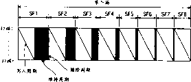
In driving the method for PDP (that is, a time-division gray level display method), be divided into a plurality of subframes (son) by with a single frames (that is, the TV field) time and change the combination of subframe, represent the intermediate gray-scale level.
For example, because the television image of NTSC standard is made up of 60 fields of per second, therefore single TV field is set to 16.7ms.Fig. 2 illustrates cuts apart the example of representing 256 gray levels with single field, vertically express time.As shown in Figure 2, a single TV field is made of eight son fields, and the ratio of the fluorescent lifetime of each son field is respectively 1,2,4,8,16,32,64 and 128.Here, change the on-state of each unit and the combination of off state, can utilize the light period in the single TV field of 256 gray level control modules by utilizing son.
Fig. 3 illustrates the drive waveforms by the above-mentioned driving circuit generation of the single son of correspondence field.
Basically, the driving method of present embodiment is identical with the classic method that is used for drive surfaces discharge PDP.At first,, provide an initialization pulse 100, thereby produce the initialization discharge in all unit in display board to scan electrode 11 at initialization cycle.By this initialization discharge, the space charge homogenising in whole, and make the wall charge storage that in the generation that writes discharge, works near data electrode 21.
Then, in write cycle, order provides negative scanning impulse 110 to scan electrode, and simultaneously, provide positive data pulse 130 according to video data to data electrode, thereby the unit in the position, point of crossing that is arranged in scan electrode that corresponding pulses is provided and data electrode produces and writes discharge (i.e. execution writes).
Then, in the cycle of keeping, replacing to scan electrode 11 and keeping electrode 12 provides high voltage to keep pulse 401 and 402.Thereby only in the unit that writes the discharge generation, repeat to produce discharge, and by utilizing this luminous realization image of keeping discharge generation to show.Then, in keeping the erase cycle of all after dates,, wipe owing to keeping discharge and be stored in wall electric charge on the dielectric layer by providing erasing pulse 403 on the electrode 12 to keeping.
Drive waveforms and driving circuit
Below explanation is used to realize the driving circuit of above-mentioned waveform.
As shown in fig. 1, this PDP display device comprises that scanning impulse produces circuit 50, and being used for order provides scanning impulse to a plurality of scan electrodes 11; Initialization/keep pulse-generating circuit 60 is used for initialization pulse being provided jointly and keeping pulse to a plurality of scan electrodes 11; Keep/erasing pulse produces circuit 70, and being used for provides jointly and keeps pulse and erasing pulse to a plurality of electrodes 12 of keeping; Data pulse produces circuit 80, is used for providing data pulse according to video data to data electrode 21; Pulse control circuit 90 is used to control above-mentioned pulse-generating circuit and image data processing.
Except be each extraction view data from the view data of input, from the field picture data that this extracts, produce each view data of sub (promptly, the image in sub-fields data) the image in sub-fields data storage that also will produce is in the frame memory China and foreign countries, and the each delegation of the current image in sub-fields data of pulse control circuit 90 from be stored in frame memory ground produces circuit 80 output datas to data pulse.In addition, for example, according to the horizontal-drive signal of input image data, vertical synchronizing signal etc., pulse control circuit 90 produces trigger pips, and the trigger pip that will produce sends to pulse-generating circuit, and wherein this trigger pip is indicated the application sequential of multiple pulse.
According to the trigger pip that pulse control circuit 90 sends, pulse-generating circuit 50,60,70 and 80 provides multiple pulse to electrode 11,12 and 21.
Scanning impulse produces circuit 50 and initialization/keep pulse-generating circuit 60 to be connected as follows, thereby the output that promptly utilizes circuit 60 is as supposing earth level Vg function circuit 50.One FET53 and a FET54 of one power supply 51, a capacitor 52, circuit 50 are provided near circuit 50 in addition.
In write cycle, FET53 is " connection ", and FET54 is " shutoff ", and in other cycle, FET53 is " shutoff ", and FET54 is " connection ".Like this, power supply 51 only provides energy to circuit 50 in write cycle.
And, in write cycle, utilize capacitor 52 that the reference potential (that is, the reference potential that the p among Fig. 1 is ordered) of scan electrode 11 is remained on electromotive force Vt, according to this reference potential, it is the negative scanning impulse (see figure 3) of (Vt-Vg) that circuit 50 provides amplitude.
Lower part will describe data pulse in detail and produce circuit 80, circuit 80 comprises line storage 81 (see figure 6)s that are used for temporary storaging data, the image in sub-fields data of the each delegation of this data representation input (promptly, for each data electrode 21 video data electrode is data of " connection " or " shutoff "), circuit 80 be used for write cycle concurrently to a plurality of data electrode 21 output data pulses.
Operation in write cycle
Fig. 4 illustrates the scan electrode 11 among the PDP1 and the position of data electrode 21.In Fig. 4, the region representation discharge cell that the electrode of being represented by square 11 and 21 intersects each other and extends.These unit are the luminous least unit of panel.
From the top to the bottom according to X0, X1 ..., Xn-1, Xn, Xn+1 ... order a plurality of scan electrodes 11 of providing along continuous straight runs to extend.From the left side to the right side according to Z0, Z1 ..., Zm-1, Zm, Zm+1 ... order a plurality of data electrodes 21 that vertically extend are provided.
Here, in instructions of the present invention, used X0, X1 ..., Xn-1, Xn, Xn+1 ... and Z0, Z1 ..., Zm-1, Zm, Zm+1 ... the time, be positioned at unit that scan electrode Xn and data electrode Zm intersect extended spot (promptly, the unit that scribbles shade among Fig. 4) be designated as " connection " unit, other unit is designated as " shutoff " unit.
Fig. 5 illustrates the example of the drive waveforms of the scanning that is provided among Fig. 4 and data electrode.
As shown in Figure 5, when when scan electrode Xn provides scanning impulse 110c, provide data pulse 130 to data electrode Xm corresponding to this on-unit, and, and provide data pulse 130 to the data electrode Xm that correspondence is turn-offed the unit when respectively when scan electrode Xn-2, Xn-1, Xn+1 provide scanning impulse 110a, 110b and 110d.
Keep as shown in Figure 3 ,/erasing pulse produces circuit 70, and amplitude is provided is that positive the keeping of Ve writes pulse 120 to keeping electrode 12 in write cycle.Write pulse 120 and keep discharge thereby provide to keep when writing to produce to write when discharge takes place, thus on the dielectric layer of keeping on the electrode 12 the negative wall electric charge of storage.
Here, be provided the unit of the scan electrode of scanning impulse 110 for correspondence, produce in on-unit and write discharge, produce in turn-offing the unit and write auxiliary discharge (calling " auxiliary discharge " in the following text), the amplitude of auxiliary discharge writes for being not enough to.This writes to discharge to cause to produce to write in on-unit keeps discharge, writes thereby finish.On the other hand, even produce auxiliary discharge in turn-offing the unit, the amplitude of this auxiliary discharge also is not enough to produce to write keep discharge.
Write priming particle that discharge or auxiliary discharge produce by this and also flow in the unit of scan electrode that the corresponding next one will be applied in scanning impulse (that is, contiguous) corresponding to the unit of the scan electrode that current scanning impulse is provided and unit in its lower section.
Subsequently, when downward one scan electrode provides scanning impulse, become corresponding to the state of the unit of this scan electrode and can produce discharge (promptly, the priming particle that flows into these unit can help produce and write discharge), thereby only in the very short time period after applying scanning and data pulse, in this on-unit, produce and write discharge (that is, this structure can make and write discharge time-delay reduction).
Like this, according to this structure, scanning and data pulse can be set as and have very short pulse width (that is, about 1.0 μ seconds), compare with traditional write time section, and the length of write cycle can shorten, and can suppress the generation that mistake writes.
Following description relates to the structure of driving circuit, and this driving circuit is by optionally providing data pulse and satellite pulse to carry out above-mentioned driving to data electrode 21.
As shown in Figure 6, except being used to produce the data pulse generator 82 of data pulse, data pulse produces circuit 80 and comprises, for each data electrode, is used to produce the satellite pulse generator 83 of satellite pulse; Be used for optionally operating the switch 84 (Fig. 6 only illustrates the structure of the data electrode of the leftmost side that is positioned at panel, other data electrode incomplete structure) of two pulse generators 82 and 83.
When the corresponding data in being stored in line storage 81 is represented " connection ", thereby switch 84 driving data pulse generators 82 provide data pulse to data electrode 21, when the corresponding data in being stored in line storage 81 is represented " shutoff ",, switch 84 provides satellite pulse to data electrode 21 thereby driving satellite pulse generator 83.
According to the above-mentioned embodiment of the invention, can use panel construction identical and basic driver method, thereby in the length that reduces the write time section, realize that high quality graphic shows with conventional art.
Embodiment 1-2
According to identical among the structure of the PDP display device of present embodiment and the embodiment 1-1.
In addition, write cycle to corresponding to identical among the data electrode satellite pulse that applies and the data pulse that applies to data electrode of turn-offing the unit and the embodiment 1-1 corresponding to on-unit.
In embodiment 1-1, the pulse width of satellite pulse is made as pulse width less than data pulse.But, in the present embodiment, the average voltage absolute value of satellite pulse is made as average voltage absolute value less than data pulse.Here, satellite pulse and data pulse all have positive polarity and mean that average voltage absolute value with satellite pulse is set at the value than the average voltage absolute value " lower " of data pulse.
Since the auxiliary discharge that in shutoff unit, produces corresponding to the scan electrode that applies scanning impulse on amplitude less than writing discharge, even therefore when waveform such as above-mentioned being conditioned, also can realize with embodiment 1-1 in identical effect.
The object lesson of satellite pulse waveform shown in Fig. 7 A-7C.
In the example shown in Fig. 7 A, though the pulse width of satellite pulse 150a, 150b...... is different with data pulse 130 essence, the wave height of satellite pulse is set as the wave height less than data pulse 130.
In the example shown in Fig. 7 B, the waveform of satellite pulse is the triangular wave form.
Waveform with triangular wave shape can allow progressively to produce auxiliary discharge, therefore, can suppress to allow the Weak-luminescence of auxiliary discharge.And the deterioration of contrast is minimized.
In the example shown in Fig. 7 C, the waveform of satellite pulse is the train of impulses form.
Also have here, the waveform with train of impulses shape can allow auxiliary discharge progressively to produce, and therefore, can suppress to allow the Weak-luminescence of auxiliary discharge.And the deterioration of contrast is minimized.
Embodiment 1-3
In embodiment 1-1, in all eight that form one single sub (SF1-SF8), to providing satellite pulse corresponding to the data electrode that turn-offs the unit.But, in the present embodiment, has relative higher brightness weighting (promptly, SF1-SF5) in the son field, provide satellite pulse to data electrode corresponding to the shutoff unit, otherwise, has relatively low luminance weighted son field (promptly, SF6-SF8) in write cycle, write pulse (that is, not providing satellite pulse) to these data electrodes to only providing corresponding to the data electrode that turn-offs the unit.
In other words, as shown in Figure 8, when when scan electrode Xn provides scanning impulse 110c, provide data pulse 130 to data electrode Zm in a son SF1-SF8 any corresponding to on-unit, thereby the unit is write, though, only in a son SF1-SF5, provide satellite pulse 150a, 150b......, and do not provide satellite pulse to data electrode Zm at a son SF6-SF8 to data electrode Zm for turn-offing the unit.
According to the method that drives this panel, even shortened write cycle, also can in having the son field of higher brightness weighting, effectively write (that is, great majority are that human eye is visible) owing to implement auxiliary discharge, like this, can realize that under the situation that does not have mistake to write high quality graphic shows.
On the other hand, though do not make in this a little and may always effective execution write owing in the son field that has than the low-light level weighting, producing auxiliary discharge, even but this low-light level weighting of a little means that mistake has taken place really to be write, but visually almost do not have harmful effect.
In addition, compare with embodiment 1-1, this structure makes the decreased number of the auxiliary discharge that produces in each.Accordingly, may suppress as because the reduction of the contrast that causes of auxiliary discharge or because the dysgenic appearance such as energy consumption increase that the frequency increase of charging of carrying out between as the scan electrode of capacity load and data electrode and discharge causes.
In order to realize above-mentioned driving method, data pulse produces circuit 80 can comprise the switch that is used to open and close satellite pulse generation circuit 83.Here, this switch can be set as " opening " in a son SF1-SF5, can be set as " closing " in a son SF6-SF8.
Embodiment 1-4
According to present embodiment, when the view data of each was brighter relatively, (Fig. 5) provided satellite pulse in turn-offing the unit described in embodiment 1-1, even when image is very dark, also do not provide satellite pulse.
For example, can by determine one be subjected in single the total number of the unit of photograph whether surpassed unit among the PDP1 total number 10%, judge whether the view data in each is bright.Here, " in a unit that is subjected to photograph in single " is meant the unit that removes in all sons in one single the shutoff unit.That is, exist on-unit to be defined as " being subjected in single " here in one of lucky son field in the field according to the unit.
Only just can realize following effect by when the view data in this is brighter relatively, producing auxiliary discharge.
Bright image is compared with dark image, and the influence that the mistake of image writes is relatively large.Accordingly, in the present embodiment, if, produce auxiliary discharge when just thinking that image is bright image and suppress mistake and write, can realize that acceptable high-quality image shows.
On the other hand, in turn-offing the unit, produce auxiliary discharge can produce faint luminous, thereby reduce contrast.The reduction of the contrast that this Weak-luminescence causes is bigger with respect to dark image.Accordingly, by when image is dark image, not producing auxiliary discharge, can keep contrast in the present embodiment.
Like this, in the present embodiment,, can realize the improvement of picture quality by when keeping contrast, preventing that mistake from writing.
In addition, owing to compare with embodiment 1-1, the decreased number of auxiliary discharge, so present embodiment is capable of reducing energy consumption.
Be provided for realizing the circuit of above-mentioned driving method below.
In data pulse produces circuit 80, can provide a switch, be used for " opening " or " closing " data pulse generator 83, an on-unit counter can be provided in the pulse control circuit 90, be used for the number at one single on-unit is counted.
Here, when the total number by the on-unit of on-unit rolling counters forward (for example surpasses a predetermined reference value, the sum of the unit among the PDP1 10%) time, this switch can be set as " opening ", when the total number by the on-unit of on-unit rolling counters forward be less than or equal to the unit among the PDP1 sum 10% the time, this switch can be set as " cutting out ".
Embodiment 1-5
Though in embodiment 1-1, in write cycle, produce auxiliary discharge in all shutoff unit, in the present embodiment, only produce auxiliary discharge near the shutoff unit that is arranged in the on-unit.
Fig. 9 illustrates the drive waveforms that is applied to each electrode according to present embodiment.
As shown in Figure 9, provide scanning impulse 110a, 110b, 110c and 110d to scan electrode Xn-2 to the Xn+1 order respectively.
And, when scanning impulse 110c is provided, provide data pulse 130 to data electrode Zm corresponding to on-unit.
In turn-offing the unit, on the other hand, when scanning impulse is provided, provide satellite pulse 150 to data electrode Zm-1, Zm and Zm+1 corresponding near the shutoff unit this on-unit.But, not to provide corresponding to the data electrode that is not positioned near the shutoff unit this on-unit satellite pulse 150 (that is, though not shown in Figure 9, also have other data electrode except Zm-1, Zm, Zm+1).
Like this, even on as described satellite pulse is defined as and only is applied to those and is positioned near the on-unit shutoff unit, but still can utilize the priming particle that writes at least one generation in discharge and the auxiliary discharge that produces near the on-unit of on-unit before being written into the unit, be implemented in that generation writes discharge in this on-unit.Accordingly, under the situation that mistake writes not occurring, realize among ability that high quality graphic shows and the embodiment 1-1 identical.
On the other hand, owing to do not have to not providing satellite pulse near the shutoff unit on-unit according to present embodiment, therefore turn-off in unit at these and can not produce auxiliary discharge, therefore the Weak-luminescence that is caused by auxiliary discharge is only limited near this on-unit unit to the influence of contrast.
In addition, compare, produce the decreased number of the unit of auxiliary discharge in the present embodiment, thereby can realize cutting down the consumption of energy with the embodiment 1-1 that in all unit, produces auxiliary discharge.
The method of " being positioned near the shutoff unit of this on-unit " and " not being positioned near the shutoff unit of this on-unit " is distinguished in explanation now.
For when on-unit is written into, at this on-unit (promptly, be arranged in the unit of electrode Xn and Zm infall) realize writing the generation of the priming particle of discharge, most important unit is provided the adjacent unit (that is the unit of the infall of electrode Xn-1 and Zm) of scanning impulse for this front at on-unit.
Therefore, here " be arranged in this on-unit near shutoff unit " be appreciated that indication near unit sequence is positioned at an on-unit or its at least one above adjacent turn-off unit.
In order to provide an object lesson, if only be positioned near this on-unit or the shutoff unit of its adjacent top is called as " be positioned at on-unit near shutoff unit ", then all other shutoff unit is appreciated that " be not positioned at on-unit near shutoff unit ".Perhaps, if, as shown in the example of Fig. 8, be positioned at this on-unit shutoff unit on every side and be called as " near the shutoff unit this on-unit ", then all other shutoff unit should be understood that " not being positioned near the shutoff unit of this on-unit ".
The following describes the circuit of realizing said method.
Data pulse shown in Figure 6 produces circuit 80 can make line storage 81 storages, the sweep trace that provides except scanning impulse is current, relates to the sub-field information of a plurality of sweep traces that are close to described sweep trace.
In addition, in data pulse produces circuit 80, provide judging unit, be used for access line storer 81, thus each unit of judging the corresponding current sweep trace that is written into whether be positioned at an on-unit near.
When the corresponding data in being stored in line storage 81 is represented " opening ", the switch 84 driving data pulse generators 82 of corresponding each data electrode 21, data pulse is provided for this data electrode.On the other hand, when the corresponding data in being stored in line storage 81 was represented " pass ", switch 84 was at first with reference to the judgement of judging unit.If judge " unit be positioned at on-unit near ", then this switch operation provides satellite pulse with driving data pulse generator 82 to data electrode, if judge " unit be not positioned at on-unit near ", does not then provide this satellite pulse.
Embodiment 2-1
The structure of the PDP display device of present embodiment is identical with the embodiment 1-1 shown in Fig. 1.
Figure 10 A illustrates the drive waveforms that is provided to electrode according to present embodiment in PDP1.
Shown in Figure 10 A,, provide data basis pulses 131 to all data electrodes simultaneously in write cycle according to present embodiment.
And, provide scanning impulse 110a, 110b, 110c and 110d to scan electrode Xn-2 to the Xn+1 order respectively, though, provide the data pulse 132 that is superimposed upon on the data basis pulses 131 to data electrode Zm corresponding to on-unit when when scan electrode Xn provides scanning impulse 110c.
Here, during write cycle, the voltage of keeping electrode is remained on an average rank.
Figure 10 B illustrates a comparative example of drive waveforms.Here, in write cycle, only provide data pulse 130 (that is, not providing data basis pulses 131) to data electrode.
Figure 11 illustrates the relation of the electric potential difference that the driving method according to present embodiment produces between each electrode in write cycle.
The setting of the amplitude of data basis pulses 131 and data pulse 132 is described now with reference to Figure 11.
When data pulse 132 be superimposed upon the amplitude that takes place when being provided on the data basis pulses 131 (, pulse 131 and 132 combined magnitude) be set to: (i) be applied in the scan electrode of scanning impulse 110 and provided the electric potential difference 203 between the data electrode of data basis pulses 131 and data pulse 132 enough high simultaneously, write discharge (promptly thereby can produce, much larger than the spark discharge voltage 201 between scan electrode and the data electrode), (ii) be applied in the scan electrode of scanning impulse 110 and only be applied in 204 of electric potential differences between the data electrode of data basis pulses 131 a little more than the spark discharge voltage between scan electrode and the data electrode 201 (that is, be lower than need to produce the voltage that writes discharge).
Scan electrode and keep electric potential difference 205 between the electrode and be set to and be no more than scan electrode and keep spark discharge voltage 202 between the electrode.
By carrying out above-mentioned setting, the voltage that is applied to data electrode shown in Figure 10 A is higher than the comparative example shown in Figure 10 B.This makes can realize following effect in write cycle.
Owing in on-unit, provide data pulse corresponding to the current scan electrode that is applied in scanning impulse, therefore, electric potential difference 203 between scan electrode and the data electrode has surpassed the spark discharge voltage 201 between scan electrode and the data electrode greatly, and the result produces to write discharge.Write the discharge initiation and produce to write by this then and keep discharge, thereby realize writing.
On the other hand, though in the shutoff unit of the unit of the current scan electrode that is applied in scanning impulse of correspondence, only provide scanning impulse (promptly, do not provide data pulse), but 203 summaries of the electric potential difference between scan electrode and the data electrode surpass the spark discharge voltage 201 between scan electrode and the data electrode, consequently produce auxiliary discharge.Because this auxiliary discharge ratio writes a little less than the discharge, therefore can not write, can not cause to write simultaneously yet and keep discharge.
Enter equally corresponding to being applied in the unit of scan electrode of scanning impulse (promptly by auxiliary discharge that takes place in the unit corresponding to the current scan electrode that is applied in scanning impulse or the priming particle that writes discharge generation at the next one, be adjacent to corresponding current unit and the unit of order under this unit that is applied in the scan electrode of scanning impulse), thus the space within these unit can produce discharge.
Accordingly, only in the short time period that begins after these unit provide scanning impulse and data pulse, in this on-unit, produce and write discharge.Like this, even have short pulse width when scanning and data pulse are set at when (that is, being approximately for 1.0 μ seconds), can suppress the generation that mistake writes.That is, can realize in the time span that high-quality image shows write cycle in shortening.
In order to realize being used for be added to circuit structure on the data basis pulses 131 of data pulse 132, data pulse shown in Figure 1 produces circuit 80 is used to produce the data basis pulses except the data pulse generator can also comprise data basis pulse generator, and data pulse and data basis pulses can all be applied to data electrode.With data pulse and data basis superimposed pulses, can relatively easier high voltage be offered data electrode by as mentioned above.
The amplitude of auxiliary discharge is described now.
Whenever when scan electrode provides scanning impulse, generation write the discharge or auxiliary discharge all will produce luminous.The figure 210 of Figure 10 A illustrates the luminous intensity when for example utilizing photodiode to pass through discharge that oscilloscope measurement data electrode Zm produces luminous, and this oscillograph is with each scan electrode of proceeding measurement.
Figure 210 illustrates by turn-offing less luminescence peak 211 that the auxiliary discharge that produces in the unit causes and being write discharge and write and kept the relatively large luminescence peak 212 that discharge causes by what produce in the on-unit.Wherein, utilize identical mark luminescence peak 211 shown in Figure 11 and 212.
Though the size of luminescence peak 211 and 212 changes with the variation in the waveform, be effectively if produce in the wrong abundance that writes priming particle in the generation of inhibition, then the luminous rank ratio of peak value 211 and peak value 212 preferably is set as and is equal to or greater than 1/100.On the other hand,, the reduction of mistake addressing and contrast can take place then, so this ratio remains on preferably and is not more than 1/10 if this ratio increases.
Wherein, in the figure 210 of the luminous intensity in this comparative example shown in Figure 10 B, though owing in turn-offing the unit, can not produce auxiliary discharge, therefore can not observe luminescence peak 211, write discharge and write the luminescence peak 212 of keeping discharge generation but can observe by what produce in the on-unit.
Embodiment 2-2
Structure according to the PDP display device of present embodiment is identical with embodiment 1-1 shown in Figure 1.
Figure 12 illustrates the drive waveforms that is provided to the electrode among the present embodiment PDP1.
According to present embodiment, as shown in figure 12, write cycle continuous provide one scan basis pulses 111 to all scan electrodes 11, and order provides the scanning impulse 122a-122d of stack scanning basis pulses 111 to scan electrode Xn-2, Xn-1, Xn and Xn+1.
Wherein, when when scan electrode Xn provides scanning impulse 112c, provide data pulse 130 to data electrode Zm simultaneously corresponding to this on-unit.
In addition, during write cycle, continuous to keep electrode 12 provide have with scanning basis pulses 111 identical polars keep basis pulses 121.
In the driving method of present embodiment, the relation of the electric potential difference in write cycle between the different electrodes is same as shown in Figure 11.
In other words, when amplitude that stack on scanning basis pulses 111 occurs during scanning impulse 112 is set as: (i) be applied in the scan electrode of scanning basis pulses 111 and scanning impulse 112 simultaneously and be applied in the enough height of electric potential difference 203 between the data electrode of data basis pulses 130, can produce and write discharge, (ii) be applied simultaneously the scan electrode of scanning basis pulses 111 and scanning impulse 112 and be not applied in 204 of electric potential differences between the data electrode of data pulse 130 a little more than the spark discharge voltage between scan electrode and the data electrode (that is, be lower than need to produce the voltage that writes discharge).
In addition, the amplitude of keeping basis pulses 121 is set as to make and is applied in the electric potential difference between the electrode kept of keeping basis pulses 121 and is lower than scan electrode 11 and keeps spark discharge voltage between the electrode 12.
By carrying out above-mentioned setting, as shown in figure 12, the absolute value that is applied to the voltage on the scan electrode is higher than the comparative example among Figure 10 B.This makes can realize the effect identical with embodiment 2-1 in write cycle.
In other words, owing in on-unit, provide data pulse corresponding to the current scan electrode that is applied in scanning impulse 112, therefore the electric potential difference between scan electrode and the data electrode has surpassed scan electrode greatly and has kept spark discharge voltage between the electrode, consequently produces and writes discharge.Write the discharge initiation and produce to write by this then and keep discharge, write thereby carry out.
On the other hand, though in turn-offing the unit, only provide scanning impulse (promptly, data pulse is not provided), but the electric potential difference between scan electrode and the data electrode only slightly exceeds scan electrode and keeps spark discharge voltage between the electrode, consequently produces auxiliary discharge.This auxiliary discharge is not enough to cause to write keep discharge.
Enter equally corresponding to will being applied in the unit of scan electrode of scanning impulse by auxiliary discharge that takes place in the unit corresponding to the current scan electrode that is applied in scanning impulse or the priming particle that writes discharge generation, thereby the space within these unit can produce discharge at the next one.Therefore, even have very short pulse width when scanning and data pulse are set at when (that is, being approximately for 1.0 μ seconds), also can suppress the generation that mistake writes.
In order to realize on the above-mentioned scanning basis pulses 111 that scanning impulse 112 is added to, can provide scanning basis pulses generator in pulse-generating circuit 60 (see figure 1)s in initialization/keep, be used to provide scanning basis pulses 111, the structure of circuit 60 can be scanning impulse 112 to be added to scan on the basis pulses 111.In order to provide and to keep basis pulses 121 to keeping electrode, keeping in addition ,/erasing pulse produces and can comprise in the circuit 70 and keep the basis pulses generator.
And, on the scanning basis pulses that as mentioned above scanning impulse is added to, can relatively easier provide high voltage to scan electrode.
In the present embodiment, as embodiment 2-1, the figure 210 of Figure 12 illustrates by turn-offing the auxiliary discharge that produces in the unit and causes Weak-luminescence peak value 211 and write discharge and write and being kept discharge and cause relatively large luminescence peak 212 by what produce in the on-unit.Wherein, the luminous rank ratio of peak value 211 and peak value 212 is preferably set to and comprises in 1/100 to 1/10 the scope.
Embodiment 2-3
Structure according to the PDP display device of present embodiment is identical with the embodiment 1-1 shown in Fig. 1.
Figure 13 illustrates the drive waveforms that is provided to according to the electrode among the PDP1 of present embodiment.
The driving method of present embodiment is basic identical with the conventional ADS driving method, as shown in figure 13, provide scanning impulse 113a to 113d to the scan electrode order, though, provide data pulse 130 to data electrode Zm simultaneously corresponding to on-unit when when scan electrode Xn provides scanning impulse 113c.
In addition, in the time period of write cycle, to keep electrode 12 provide have with scanning basis pulses 111 identical polars keep basis pulses 121.
In the present embodiment, as described below, the amplitude of scanning impulse 113a-113d is set as great amplitude greater than the scanning impulse that provides in the comparative example shown in Figure 10 B.
The amplitude of scanning impulse 113 is set at electric potential difference between the data electrode that makes the scan electrode that is provided scanning impulse 113 and be provided data pulse greater than the spark discharge voltage between this scan electrode and the data electrode, but still is lower than to produce to write and keeps the required voltage of discharge.
The amplitude of data pulse 130 is set at: be provided the scan electrode of scanning impulse 113 and the electric potential difference that is provided between the data electrode of data pulse can allow to produce to write to keep discharge.
In addition, the amplitude of keeping basis pulses 121 is set at: be provided the scan electrode of scanning impulse 113 and be provided keep basis pulses keep electric potential difference between the data electrode less than this scanning with keep spark discharge voltage between the electrode.
By above-mentioned setting, in write cycle, the relation of the electric potential difference between the different electrodes is same as shown in Figure 11.
In other words, owing in on-unit, provide data pulse corresponding to the current scan electrode that is applied in scanning impulse 113, therefore the electric potential difference between scan electrode and the data electrode has surpassed scan electrode greatly and has kept spark discharge voltage between the electrode, consequently produces and writes discharge.Write the discharge initiation and produce to write by this then and keep discharge, write thereby carry out.
On the other hand, though in turn-offing the unit, only provide scanning impulse (promptly, data pulse is not provided), but the electric potential difference between scan electrode and the data electrode only slightly exceeds the spark discharge voltage between scan electrode and the data electrode, consequently produces auxiliary discharge.This auxiliary discharge is not enough to cause to write keep discharge.
Write discharge owing to produce in on-unit, to produce in turn-offing the unit and be not enough to realize the auxiliary discharge that writes, therefore, the priming particle still enters corresponding to the next one and will be provided in the unit of scan electrode of scanning impulse.Therefore, even when scanning and data pulse are set as and have very little pulse width (be about 1.0 μ second), also can suppress the generation that mistake writes.
In the present embodiment, as embodiment 2-1, the figure 210 among Figure 13 illustrates by turn-offing the auxiliary discharge that produces in the unit and causes Weak-luminescence peak value 211 and write discharge and write and being kept discharge and cause relatively large luminescence peak 212 by what produce in the on-unit.Wherein, the luminous rank ratio of peak value 211 and peak value 212 is preferably set to and comprises in 1/100 to 1/10 the scope.
Embodiment 3-1
The structure of PDP display device
Basically the PDP1 about embodiment 1-1 with shown in Figure 1 is identical according to the structure of the PDP display device of present embodiment.
Figure 14 illustrates the structure of the PDP display device of present embodiment.
Though the structure of the PDP2 in the PDP display device is basic identical with embodiment 1-1 shown in Figure 1, and the auxiliary discharge electrode 31 that is adjacent to and is parallel to scan electrode 11 also is provided.
Figure 15 is the structural section figure along A-A ' of PDP2 shown in Figure 14.
In PDP2, provide a front glass substrate 10 and a back glass substrate that has certain intervals therebetween has been installed toward each other.
On the apparent surface of front glass substrate 10, have the scan electrode 11 that is arranged in parallel with each other, keep electrode 12 and auxiliary discharge electrode 31, on these electrodes, be coated with dielectric layer 14 and protective seam 15.Scan electrode 11 is formed by transparent electrode layer 11b and the bus electrode layer 11a that is layered on the transparent electrode layer respectively.Keeping electrode 12 forms by transparent electrode layer 12b and the bus electrode layer 12a that is layered on this transparent electrode layer.Auxiliary discharge electrode 31 all is adjacent to the bus electrode layer 11a of scan electrode, and on shielding film 32.
Interval between each auxiliary discharge electrode 31 and the scan electrode 11 is less than each scan electrode and keep interval between the electrode, and can produce auxiliary discharge when being set to electric potential difference when the amplitude that scanning impulse occurs approaching (Vt-Vg).
On the other hand, on the apparent surface of back glass substrate, be arranged with the data electrode 21 with scan electrode 11 quadratures, and provide dielectric layer 23 and phosphor layer 24 with covers data electrode 21.
Driving method and driving circuit
Figure 16 illustrates the drive waveforms that is applied to the electrode among the PDP2.
Be applied to scan electrode 11, keep described in the waveform such as embodiment 1-1 of electrode 12 and data electrode 21, and the operation of these electrodes is identical with drive waveforms among the traditional three electrode A C type surface-discharge PDP.
As shown in figure 14, the driving circuit of the PDP display device of present embodiment is identical with embodiment 1-1 shown in Figure 1, and auxiliary discharge electrode 31 links to each other with this driving circuit at a P among Figure 14.
Described in embodiment 1-1, in the driving circuit of present embodiment, in write cycle, FET53 is " connection ", and FET54 is " shutoff ", and in all other stages, FET53 is " connection ", and FET54 is " shutoff ".
Accordingly, initialization pulse is provided and keeps pulse to auxiliary discharge electrode 31 from initialization/keep pulse-generating circuit 60 respectively at the initialization cycle and the cycle of keeping.And, do not provide scanning impulse to auxiliary discharge electrode in write cycle.
In other words, except not providing the scanning impulse in write cycle, the waveform that provides to auxiliary discharge electrode 31 is identical with the waveform that offers scan electrode 11, i.e. initialization pulse 100 and keep pulse 141 and all be provided for scanning impulse 11 and auxiliary discharge electrode 31.
Below with reference to the generation of Figure 17 A-17C explanation discharge in the face degree etc. in write cycle.
Therefore described in embodiment 1-1, scanning impulse is that negative polarity and amplitude are (Vt-Vg), when this scanning impulse is offered scan electrode, electric potential difference (Vt-Vg) occurs between scan electrode and the adjacent auxiliary discharge electrode.
Accordingly, shown in Figure 17 A, between scan electrode and adjacent auxiliary discharge electrode, produce auxiliary discharge, shown in Figure 17 B, in the discharge space of the unit that auxiliary discharge takes place, produce space charge.
Wherein, when the scan electrode in on-unit provides scanning impulse, to providing data pulse to data electrode that should on-unit.Wherein and since above-mentioned auxiliary discharge cause produce a large amount of charged particle at on-unit, therefore shown in Fig. 7 C, after applying scanning and data pulse, in on-unit only very short time just effectively generation write discharge.
On the other hand, in turn-offing the unit, only provide scanning impulse, and not to providing data pulse to the data electrode that should turn-off the unit.Accordingly, can therefore can not produce and write discharge in this scan electrode 11 and electric potential difference between the data electrode 21 of turn-offing in the unit above the spark discharge voltage between this scanning and the data electrode.
According to the driving method of present embodiment,, thereby suppress the wrong generation that writes even when the pulse width with scanning and data pulse is made as very little (approximately, promptly 1.0 seconds), also can effectively produces and write discharge.
Interval between each auxiliary discharge electrode 31 and the scan electrode 11 is preferably such width: when the electric potential difference between auxiliary discharge electrode 31 and the scan electrode 11 is equal to or greater than (Vt-Vg)/2, can produce discharge.Here, this interval preferably is set as between the 10 μ m-50 μ m.
Usually, when producing discharge between the very near electrode of distance, because ion sputtering, near the film these electrodes can be degenerated.But, according to present embodiment, in one single (1/60 second), only producing the very auxiliary discharge of peanut, therefore in fact can't take place because the degeneration of the performance of the protective seam 15 that ion sputtering causes.
In addition, because auxiliary discharge can produce very faint luminous, and because in one during the demonstration of black level (black level) auxiliary discharge at least several times can take place, therefore because the increase of the black level brightness that occurs when producing auxiliary discharge is easy to occur the reduction of contrast.But,,, therefore can suppress because the luminous contrast that causes of auxiliary discharge reduces owing to below each auxiliary discharge electrode 31, have shielding film 32 according to present embodiment.
In addition, owing to provide identical waveform to scan electrode 11 with auxiliary discharge electrode 31, so can use initialization/keep pulse-generating circuit 60 to provide these waveforms to electrode 11 and 31 in initialization cycle and the cycle of keeping.In addition and since write cycle auxiliary discharge electrode 31 electromotive force be maintained at electromotive force Vt, therefore do not need the driving circuit that provides other especially, thereby this device can be provided with relatively low cost.
Structure in the electrode extended area
The structure of the electrode in the electrode extended area of face plate edge below with reference to Figure 18 A and 18B explanation.
Figure 18 A illustrates the part of PDP2, and this PDP2 comprises front glass substrate 10, back glass substrate 20, sealing unit 16, scan electrode 11, keeps electrode 12 and auxiliary discharge electrode 31.
In the present embodiment, shown in Figure 18 A, each auxiliary discharge electrode 31 in face utmost point viewing area (that is, by the zone in the border of sealing unit 16 signs) and the interval D 1 between the scan electrode 11 are set to very narrow, thereby are convenient to auxiliary discharge.But, near the part of this viewing area of interval sealing unit 16 (promptly, the part of drawing a circle among Figure 18 A) expansion in, auxiliary discharge electrode in this electrode extended area (that is the zone in the outside, border of sealing unit 16 signs) and the interval d1 between the scan electrode are set as greater than interval D 1.
D1 is enough wide at interval, thereby even the electric potential difference between auxiliary discharge electrode 31 and scan electrode 11 approaches (Vt-Vg), also can prevent discharge.Here, d1 is preferably between the 50 μ m-300 μ m at interval.
Accordingly, may realize a kind of like this panel construction: wherein only auxiliary discharge takes place in the viewing area, and auxiliary discharge can not take place between the adjacent electrode in the electrode extended area.
In addition, as shown in Figure 18 B, on the front glass substrate 310 of conventional prior art PDP300, interval d between the adjacent scan electrode 311 in the outside, zone (that is, in the electrode extended area) that is indicated by sealing unit 316 is less than the interval D between the adjacent scan electrode 311 in the zone that is indicated by sealing unit 316.It is very little that the advantage of this structure is that the width of the flexible printer circuit (FPC) that will contact with the electrode extended area can be set as, and is used for being connected with external circuit.
Relative, according to the present embodiment shown in Figure 18 A, the interval d2 between the adjacent scan electrode 11 in the electrode extended area is equal to or greater than the interval D 2 between the adjacent scan electrode 11 in the viewing area.This structure has following advantage.
In the PDP2 of present embodiment, the number that is formed on the auxiliary discharge electrode 31 on the front glass substrate 10 equals the number of scan electrode 11, therefore, compares with traditional PDP, and the electrode in the electrode extended area doubles.Accordingly, very little if the interval between the scan electrode 11 in the electrode extended area is set as, then the interval between the adjacent electrode in the electrode extended area will be quite little, so will produce discharge probably in the electrode extended area.But, be equal to or greater than interval between the scan electrode 11 in the viewing area by setting interval between the scan electrode 11 in the electrode extended area, can suppress to produce in the electrode extended area possibility of discharge.
Embodiment 3-2
Figure 19 illustrates the structure of the PDP display device of present embodiment.
The structure of PDP2 in this PDP display device embodiment 3-1 with shown in Figure 14 basically is identical.
As driving circuit, this panel comprises that scanning impulse produces circuit 50, is used to provide scanning impulse (that is, have with reference to the amplitude Vt of electromotive force Vt negative pulse); Keep pulse-generating circuit 61, be used to provide and keep pulse 301; Initialization pulse produces circuit 62, is used to provide initialization pulse; As the circuit that is used for providing to auxiliary discharge electrode 31 pulse, this panel comprises the initiation discharge pulse generation circuit 55 that is used for producing in write cycle the initiation discharge pulse with regular voltage Vp.
Initialization pulse generation circuit 62 utilizes the output of keeping pulse-generating circuit 61 to operate as the earth level of supposing (provisional), and scanning impulse generation circuit 50 and initiation discharge pulse produce circuit 55 and utilize the output of initialization pulse generation circuit 62 to operate as the earth level of supposing.
In addition, keep pulse-generating circuit 71 to keeping electrode 12 and providing the circuit of pulse, this panel to comprise, be used to provide and keep pulse as being used for; Keep writing pulse-generating circuit 72, be used for providing positive keeping to write pulse 120 (amplitude Ve) to keeping electrode 12, and erasing pulse generation circuit 73, be used to provide erasing pulse.
Wherein, keeping pulse-generating circuit 61 and initialization pulse produces circuit 62 and is configured to provide to auxiliary discharge electrode 31 and scan electrode 11 and keeps and initialization pulse.Use provides the circuit 61 and 62 costs that can reduce about panel circuit of pulse to electrode 11 and 31.
Keep writing pulse-generating circuit 72 utilization and keep the output of pulse-generating circuit 71 and operate as the earth level of hypothesis, erasing pulse produces circuit 73 and utilizes and keep the output that writes pulse-generating circuit 72 and operate as the earth level of hypothesis.
Wherein, write pulse when producing when writing discharge, at scan electrode with keep to produce to write between the electrode and keep discharge, thereby make and assemble negative charge on the dielectric layer on keep electrode thereby provide to keep.
In addition, this panel comprises that data pulse produces circuit 80, is used for providing data pulse according to video data to data electrode.
As top embodiment 1-1, these circuit are controlled by panel control circuit 90.
Figure 20 illustrates the drive waveforms that offers these electrodes among the PDP2 according to present embodiment.
The drive waveforms of present embodiment is identical with waveform among the embodiment 3-1 shown in Figure 16, but with provide the embodiment 3-1 of the voltage Vt of the reference voltage level that equals scan electrode 11 to compare in write cycle to auxiliary discharge electrode 31, in the present embodiment, determine to offer the voltage Vp of auxiliary discharge electrode 31 in write cycle by the wave height of the initiation discharge pulse 160 that causes 55 generations of discharge pulse generation circuit.
Accordingly, cause discharge pulse produce circuit 55 can free setting voltage Vp, so this voltage Vp may be set as the value that is higher than voltage Vt.
Here, the interval between scan electrode 11 and the auxiliary discharge electrode 31 must be set at electric potential difference Vd2 between the scan electrode that makes auxiliary discharge electrode and be applied in scanning impulse (=Vp) a little more than the spark discharge voltage between this auxiliary discharge electrode and the scan electrode.Like this, voltage Vp high-voltage value can be set at, thereby degree of freedom to a certain degree can be in the setting at the interval between auxiliary discharge electrode and the scan electrode, allowed.
In other words, set being spaced apart between scan electrode 11 and the auxiliary discharge electrode 31: when the electric potential difference between scan electrode and the auxiliary discharge electrode is (Vp-Vt), between these two electrodes, do not discharge, when the electric potential difference between scan electrode and the auxiliary discharge electrode be Vd2 (=Vp) time, between these two electrodes, discharge.Accordingly, setting voltage Vp is that high value can allow scan electrode 11 and auxiliary discharge electrode 31 at a distance of more farther.
When waveform shown in Figure 20 was provided in PDP2, during write cycle, the generation of the discharge in panel etc. was identical with the description with reference to the embodiment 3-1 of Figure 17.That is,, between scan electrode and auxiliary discharge electrode, produce auxiliary discharge whenever when scan electrode provides scanning impulse.Because this auxiliary discharge produces a large amount of charged particles, after being provided, data pulse is used to write that discharge takes place that the seeking time of wanting is quite short, and this writes discharge and can effectively produce.
Here, since the distance between auxiliary discharge electrode 31 and the scan electrode 11 than and the distance kept between the electrode 12 nearer, therefore, only between auxiliary discharge electrode 31 and scan electrode 11, discharge, and at auxiliary discharge electrode 31 and keep between the electrode 12 and do not discharge.
In addition, shown in the example of Figure 19, thereby, the auxiliary discharge electrode 31 shown in the example of Figure 19 can provide identical waveform to all auxiliary discharge electrodes though being connected with each other, even but auxiliary discharge electrode is not continuous each other, can be by providing identical waveform to realize identical effect to each auxiliary discharge electrode yet.
Embodiment 3-3
The structure of the PDP of present embodiment is identical with the PDP2 shown in the embodiment 3-2.Though according to present embodiment, in the cycle of keeping, auxiliary discharge electrode 31 can be made as high impedance status as shown in figure 21 or remain on as shown in figure 22 intermediate electric potential, its driving method also with embodiment 3-2 in identical.
Be as shown in figure 21 high impedance status for auxiliary discharge electrode 31 being set in the cycle of keeping, switch can be provided, be used for the connection between " connection " or " disconnection " initiation discharge pulse generation circuit 55 (seeing the drive circuit module of Figure 19) and the auxiliary discharge electrode, this switch can be made as " disconnection " in the cycle of keeping, and is made as " connection " in all other cycles.
In embodiment 3-2, because each auxiliary discharge electrode and the adjacent big electric potential difference of keeping between the electrode, therefore in the cycle of keeping, at auxiliary discharge electrode with keep between the electrode unwanted discharge can take place, this unwanted discharge can weaken or interrupt scanning electrode 11 and keep the discharge that produces between the electrode 12.But, in the present embodiment, can stop the generation of unwanted discharge by keeping auxiliary discharge electrode 31 for high impedance status in the cycle of keeping.
Here,, be preferably in and keep cycle disconnection auxiliary discharge electrode and respectively each auxiliary discharge electrode is remained on high impedance status, also auxiliary discharge electrode connected to one another can be remained on high impedance status though prevent undesirable discharge generation in order to improve.
As shown in figure 22, on the other hand, for auxiliary discharge electrode 31 being remained on intermediate electric potential in the cycle of keeping, the output that causes discharge pulse generation circuit 55 can be remained on the level of rule, this level have with keep pulsion phase with polarity but numerically less (that is, be approximately keep pulse height 1/2).
In this case, keep the level that the electromotive force of all auxiliary discharge electrodes in the cycle is maintained at the intermediate value that is similar to a scope, scan electrode 11 fluctuates (promptly in this scope with the electromotive force of keeping electrode 12, " intermediate electric potential "), big voltage can not appear at auxiliary discharge electrode 31 and adjacent keeping between the electrode 12 therefore.In the example of above-mentioned high impedance, can prevent the generation of unwanted discharge.
Here, as shown in figure 19,, make them produce circuit 55 drivings by causing discharge pulse jointly, so this circuit structure is comparatively simple because the auxiliary discharge electrode 31 among the PDP2 is connected to each other.
Embodiment 3-4
Figure 23 illustrates the structure of the PDP display device of present embodiment.
The structure of PDP2 in this PDP display device is identical with the structure of embodiment 3-1 shown in Figure 14.
The structure of driving circuit is same as shown in Figure 19, though what comprise in this structure is that second initialization pulse produces circuit 63, this circuit 63 is used for providing second initialization pulse 101 with regular amplitude (Vs) to auxiliary discharge electrode 31 at initialization cycle.
The initiation discharge pulse generation circuit 55 that is connected to of circuit utilizes the output of keeping pulse-generating circuit 61 to operate as the earth level of hypothesis, and second initialization pulse generation circuit, 63 utilization initiation discharge pulses produce the output of circuit 55 and operate as the hypothesis earth level.
Figure 24 illustrates the drive waveforms that present embodiment offers the electrode among the PDP2.The application of these waveforms is described now with reference to Figure 24.
The drive waveforms of offer scan electrode 11, keeping electrode 12 and data electrode 21 is identical with the waveform of embodiment 3-2 shown in Figure 20.
On the other hand, at initialization cycle, utilize second initialization pulse to produce circuit 63 and provide positive second initialization pulse 101 (voltage Vs), utilize in the cycle of keeping and cause discharge pulse and produce circuit 55 and provide have an amplitude Vp2 positive to keep pulse 161 (voltage Vp2) to auxiliary discharge electrode with amplitude Vs to auxiliary discharge electrode 31.Here, the amplitude Vs of second initialization pulse is lower than the amplitude of the initialization pulse that is provided to scan electrode 11.
Below with the setting at the interval between account for voltage Vp2 and scan electrode 11 and the auxiliary discharge electrode 31.
In write cycle, when providing when causing discharge pulse not providing under the situation of scanning impulse to auxiliary discharge electrode 31 to scan electrode 11, electric potential difference Vd3 appears between scan electrode and auxiliary discharge electrode, wherein Vd3=(electric potential difference that charge stored causes in the initialization cycle)+(Vp2-Vt).In addition, in write cycle, when providing scanning impulse, and provide when causing discharge pulse to auxiliary discharge electrode 31 to scan electrode 11, electric potential difference Vd4 appears between scan electrode and auxiliary discharge electrode, wherein Vd4=(electric potential difference that charge stored causes in the initialization cycle)+Vp2.
Accordingly, the width at the interval between the value of voltage Vp2 and scan electrode 11 and the auxiliary discharge electrode 31 is set as: when the electric potential difference between scan electrode 11 and the auxiliary discharge electrode 31 is Vd3, between these electrodes, do not produce discharge, and when the electric potential difference between scan electrode 11 and the auxiliary discharge electrode 31 is Vd4, between these electrodes, produce discharge.
Below description relate to when the drive waveforms that provides as shown in figure 24, in the generation of initialization and the discharge in panel etc. during write cycle.
In the present embodiment, the amplitude Vs that is applied to second initialization pulse 101 of auxiliary discharge electrode 31 is lower than the amplitude of initialization pulse 100, therefore in initialization cycle, produces preparation discharge (seeing Figure 25 A) between auxiliary discharge electrode 31 and the scan electrode 11.
Result as this preparation discharge stores positive charge on the dielectric layer on auxiliary discharge electrode 31, stores negative charge (seeing Figure 25 B) on the dielectric layer on scan electrode 11.
Then,, in write cycle, between scan electrode 11 and auxiliary discharge electrode 31, produce auxiliary discharge (seeing Figure 25 C), in discharge space, produce space charge (seeing Figure 25 D) when when scan electrode 11 provides scanning impulse.
The basic operation of this structure is identical with embodiment 3-2 with effect, even have very short pulse width when scanning impulse and data pulse are set as when (about 1.0 μ second), also can suppress the generation that mistake writes.But in the present embodiment, the smaller value that the amplitude Vp2 that causes discharge pulse is set at less than the amplitude Vp of the initiation discharge pulse among the embodiment 3-2 is possible.
In other words, (=Vp) comparative descriptions: because these two electric potential differences have all produced the voltage that only slightly surpasses the spark discharge voltage between scan electrode and the auxiliary discharge electrode, so Vd4 can be regarded as similar with Vd2 the electric potential difference Vd2 of the electric potential difference Vd4 of present embodiment and embodiment 3-2.Accordingly, the amplitude Vp2 that causes discharge pulse can be set at smaller value less than the amplitude Vp of the initiation discharge pulse that in embodiment 3-2, offers auxiliary discharge electrode 31.
Cause the proof voltage (voltage resistance) that discharge pulse produces the circuit component in the circuit 55 owing to can reduce, therefore can reduce the cost of related circuit.
In addition, the voltage that the initiation discharge pulse that the voltage that charge stored produced in initialization cycle can replenish to be provided in write cycle produces, even therefore when the amplitude Vp2 that will cause discharge pulse is made as less than the spark discharge voltage between scan electrode 11 and auxiliary discharge electrode 31, also can produce auxiliary discharge.
In addition, provide pulse because pulse-generating circuit 61 is kept in use according to present embodiment to scan electrode 11 and auxiliary discharge electrode 31, therefore compare with relating to those circuit costs that separation circuit is provided, this circuit cost is comparable to provide the cost of those circuit of separation circuit low.
The variation of present embodiment
Shown in the drive waveforms among Figure 26, by auxiliary discharge electrode 31 is set at ground potential, rather than second initialization pulse is provided, even be set at smaller value as the amplitude Vp3 that will cause discharge pulse, also can realize the effect identical with present embodiment less than amplitude Vp2.In addition, according to this variation, can omit second initialization pulse and produce circuit 63, thereby further reduce cost.
And, offer that second initialization pulse of auxiliary discharge electrode 31 is unnecessary to have positive polarity, also can be set as negative polarity.In this case, the quantity that is stored in the positive charge on the auxiliary discharge electrode 31 further increases, thereby still very low even work as the amplitude of the initiation discharge pulse that offers auxiliary discharge electrode 31, also can realize the same effect of present embodiment.
In addition, described in embodiment 3-3, remain (i) by the output that second initialization pulse is produced circuit 63 or initiation discharge pulse generation circuit 55 (seeing the drive circuit module of Figure 23) and be in high impedance status in the cycle of keeping, or (ii) in the cycle of keeping, keep pulse amplitude 1/2, can prevent the scan electrode 11 that is used to show and keep the reduction of keeping discharge or interruption between the electrode 12, can also prevent at auxiliary discharge electrode 31 and keep between the electrode 12 and discharge.
Have again, even being converted to circuit 63 with the position of causing discharge pulse generation circuit 55, second initialization pulse generation circuit 63 utilize the output of keeping pulsing circuit 61 to operate as the reference electromotive force, circuit 55 utilizes the output of circuit 63 to operate as the reference electromotive force, also can realize the above-mentioned same effect of present embodiment.
Embodiment 3-5
Figure 27 illustrates the drive waveforms of the PDP of present embodiment.Though in the present embodiment, in the time that applies scanning impulse with apply between time of data pulse and set very short section Td time delay, these drive waveforms are still with shown in Figure 16 basic identical.
Can produce the sequential that circuit 80 is exported trigger pips to data pulse by adjusting panel control circuit 90, set this time delay of section Td.
Section Td can be set as greater than 0ns and be less than or equal to 500ns time delay, was preferably to be lower than 300ns.It is the reasons are as follows.
According to this structure, after the very short delay after applying scanning impulse, produce auxiliary discharge, recombinating during this period by the space charge that this auxiliary discharge produces, and be eliminated.In addition, in order to produce fast and effectively write discharge, provide data pulse in the time of must in discharge space, also having space charge.Therefore, be preferably in auxiliary discharge and produce after the space charge, and before these space charges are eliminated, apply these data pulses.This time period is between 0ns-500ns.
Subsequently, apply data pulse, might further shorten by auxiliary discharge producing the needed time of discharge that writes by beginning to postpone 0ns-500ns after applying scanning impulse.
Wherein, in the drive waveforms shown in Figure 16, time delay section Td=0.
In addition, by in 3-4, section Td time delay being set, can realize and the described identical effect of present embodiment at embodiment 3-1 and 3-2.
Embodiment 3-6
In 3-4,, will produce auxiliary discharge between scan electrode 11 and the auxiliary discharge electrode 31 at the embodiment 3-1 that relates to PDP2 whenever when scan electrode provides scanning impulse.But, as described below in the present embodiment, undertaken some by electrode structure and adjust the generation that can further improve auxiliary discharge PDP2.
In the example shown in Figure 28 A, on the auxiliary discharge electrode 31 of unit, form the kick 33a of one or more comb shapes, described projection is outstanding to scan electrode 11.According to this structure, the interval between auxiliary discharge electrode 31 and the scan electrode 11 narrows down, so that the generation of auxiliary discharge.
In the example of Figure 28 B, form the projection 33b of broad on the auxiliary discharge electrode 31 in the unit, described projection is outstanding to scan electrode 11.According to this structure, except having dwindled the interval between auxiliary discharge electrode 31 and the scan electrode 11, also reduced the resistance value of auxiliary discharge electrode 31, like this, prevented the reduction of voltage when discharge generation, also help auxiliary discharge and take place.
In the example shown in Figure 28 C, form the projection 33c of one or more T shapes on the auxiliary discharge electrode 31 in the unit, described projection is outstanding to scan electrode 11.
In the example of Figure 28 D, form one or more L shaped projection 33c on the auxiliary discharge electrode 31 in the unit, described projection is outstanding to scan electrode 11.According to this structure, except helping to prevent to cause electrode to be burnt out the auxiliary discharge generation owing to the streaming current of superpotential electric current by the interval that dwindles between auxiliary discharge electrode 31 and the scan electrode 11.
Compare with the T type projection 33c with two ends (being the part of drawing a circle among Figure 28 c) among Figure 28 c, each only has an end the L shaped projection 33d among Figure 28 D.Here, the end ratio that is formed on on-chip electrode is easier to and substrate separation.Therefore, the end of L type projection relatively is not easy separated.
Here, in the example shown in Figure 28 A-28D, on auxiliary discharge electrode 31, form projection 33a-33d.But, even shown in Figure 28 E-28H, on scan electrode 11, form projection 33a-33d, also can realize identical effect.
Embodiment 4-1
The structure of PDP display device
Figure 29 illustrates the structure of the PDP display device of present embodiment.Figure 30 illustrates the structural section figure along B-B ' of PDP3 shown in Figure 29.
The structure of PDP3 in this PDP display device is identical with the PDP2 shown in Figure 14, but it is adjacent with scan electrode 11 with auxiliary discharge electrode among the PDP2 31, thereby the PDP2 that can produce auxiliary discharge between the auxiliary discharge electrode of scan electrode and vicinity compares, in the PDP3 of present embodiment, provide a pair of auxiliary discharge electrode (i.e. first auxiliary discharge electrode 41 and second auxiliary discharge electrode 42) at contiguous each scan electrode 11 place, this auxiliary discharge electrode is set on the shielding film 43, produces auxiliary discharge between every pair of auxiliary discharge electrode 41 and 42.
In order between first and second auxiliary discharge electrodes 41 and 42, to produce auxiliary discharge, the spacing between electrode 41 and 42 is set at the very little discharge of generation under the electric potential difference of about (Vt-Vg).Here, this spacing preferably is set as such width: when the described electric potential difference in front during more than or equal to (Vt-Vg)/2, can produce discharge.Quantitatively, equal an interior interval of 10 μ m-50 mu m ranges.
In addition, as shown in figure 29, each first auxiliary discharge electrode 41 links to each other with an adjacent scan electrode 11, and second auxiliary discharge electrode 42 is connected with each other at Figure 29 mid point P.
In full accord according to what describe among the driving circuit structure of present embodiment and the embodiment 3-1 shown in Figure 14, so present embodiment does not increase aspect circuit cost yet.
Drive waveforms and driving circuit
Figure 31 illustrates the drive waveforms of the electrode that is provided to PDP3.
The drive waveforms of be provided to scan electrode 11, keeping electrode 12 and data electrode 21 is identical with the waveform of embodiment 3-1 shown in Figure 16, and the operation of PDP3 is basic identical with traditional three electrode A C type surface-discharge PDP.And the drive waveforms that is provided on second auxiliary discharge electrode 42 is identical with the drive waveforms that is provided to auxiliary discharge electrode 31 described in the 3-1 embodiment illustrated in fig. 16.
In addition, the drive waveforms that is provided on each first auxiliary discharge electrode 41 is identical with drive waveforms on being provided to the scan electrode 11 that is close to it.Here, for first auxiliary discharge electrode 41, Figure 31 only illustrates the drive waveforms that is provided to first auxiliary discharge electrode that is adjacent to scan electrode Xn.
Below with reference to Figure 32 A-32C explanation generation in the discharge in panel during write cycle etc.
Because scanning impulse has negative polarity and amplitude is (Vt-Vg), therefore when when scan electrode 11 provides scanning impulse, electric potential difference (Vt-Vg) occurs between first auxiliary discharge electrode 41 and second auxiliary discharge electrode 42.Therefore, shown in Figure 32 A,, between first and second auxiliary discharge electrodes, produce auxiliary discharge when when scan electrode provides scanning impulse.And shown in Figure 32 B, because this auxiliary discharge produces space charge at discharge space.
On the other hand, when the scan electrode in on-unit provides scanning impulse, provide data pulse to data electrode corresponding to this on-unit.Because this auxiliary discharge causes occurring a large amount of space charges in on-unit, therefore can write discharge with effectively producing fast.Like this, even be set as and have very short pulse width (that is, about 1.0 μ seconds) when scanning impulse, also can effectively produce and write discharge.
In addition, described in embodiment 3-1, because the number of the auxiliary discharge that produces is not very big, therefore protective seam 15 performance degradations that caused by ion sputtering can not take place.In addition, owing to form shielding films, therefore can suppress the reduction of the contrast that causes by auxiliary discharge every pair first and second auxiliary discharge electrode 41 and 42 times.
Except the above-mentioned effect that realizes embodiment 3-1, present embodiment also can be realized following effect.
In embodiment 3-1, owing between auxiliary discharge electrode 31 and scan electrode 11, produce auxiliary discharge, therefore on the surface of the dielectric layer on the scan electrode 11, will store wall electric charge excessive or in shortage, this will cause defective illumination, as turn-off in the cycle of keeping the unit by according to or open the unit and do not shone.
But, in the present embodiment, owing between first and second auxiliary discharge electrodes 41 and 42 (i.e. electrode except scan electrode 11), produce auxiliary discharge, therefore, in fact auxiliary discharge to the formation of the wall electric charge on the dielectric layer on the scan electrode 11 without any influence.This means need not revise just can use the existing Driving technique that is used for traditional three electrode A C type surface-discharge PDP to scan electrode 11, keep electrode 12 and data electrode 21 carries out basic driver.
Here, example as shown in figure 30 directly forms first and second auxiliary discharge electrodes 41 and 42 of PDP3 on shielding film 43, and these electrodes are covered by dielectric layer 14 and protective seam 15.But as shown in figure 33, dielectric layer 14 and protective seam 15 can be formed on the shielding film 43, form first and second auxiliary discharge electrodes 41 and 42 then on the top of layer 14 and 15.In this case, as mentioned above,, also still can produce auxiliary discharge even directly face discharge space when first and second auxiliary discharge electrodes 41 and 42.
In addition, because the number of the auxiliary discharge that produces is few, therefore can not occur because first and second auxiliary discharge electrodes 41 that ion sputtering causes and 42 performance depreciation.In addition, because at electrode 41 and 42 times formation shielding layers, the contrast that therefore can suppress to be caused by auxiliary discharge reduces.
Structure in the electrode extended area
With reference to Figure 34 electrode structure in the electrode extended area is described below.
In the PDP3 of present embodiment, the number that is formed on first auxiliary discharge electrode 41 on the front glass substrate 10 and second auxiliary discharge electrode 42 all equals the number of scan electrode 11, therefore compare with the number of the scan electrode of traditional PD P, electrode number increases twice.
If for example, scan electrode 11 and first and second auxiliary discharge electrodes 41 and 42 all extend to the zone in sealing unit 16 outsides, then the electrode number in the electrode extended area will be 1.5 times among the embodiment 3-1 (or traditional PD P 3 times), and each electrode in the electrode extended area is connected the difficulty that will become with FPC.
But, in the present embodiment, in the zone (that is the electrode 41 that, does not have extension) that sealing unit 16 indicates, first auxiliary discharge electrode 41 links to each other with adjacent scan electrode 11, therefore extend beyond the zone that sealing unit 16 indicates electrode number will with embodiment 3-1 in identical.
Therefore, by the interval between the scan electrode in the electrode extended area 11 being set at, can prevent from the electrode extended area, to produce discharge more than or equal to the equivalence in this viewing area at interval (that is, with among the embodiment 3-1 identical).
In addition, as in embodiment 3-1, near the part of the viewing area of sealing unit 16 (being the part of drawing among Figure 34), each will be widened the interval between first and second auxiliary discharge electrodes, in the electrode extended area, the interval between these electrodes is set as very wide.
Especially, by the interval between first and second auxiliary discharge electrodes 41 and 42 in the electrode extended area being set at a width (being preferably in the scope of about 50 μ m-300 μ m), this width makes even does not also allow to produce discharge when being approximately (Vt-Vg) in electric potential difference, can prevent to discharge between first and second auxiliary discharge electrodes in the electrode extended area.
Embodiment 4-2
Figure 35 illustrates the PDP display device of present embodiment.The structure of PDP3 in this PDP display device is identical with the structure of embodiment 4-1 shown in Figure 29.
Because identical among driving circuit and the embodiment 3-2, therefore will no longer be specifically described, but in order to provide pulse to the scan electrode 11 and first auxiliary discharge electrode 41, this panel comprises the scanning impulse generation circuit 50 that is used to provide scanning impulse (amplitude is the negative pulse of Vt when being reference potential Vt), be used to provide keep pulse keep pulse-generating circuit 61, and be used to provide the initialization pulse of initialization pulse to produce circuit 62.In addition, in order to provide pulse to second auxiliary discharge electrode 41, this panel comprises that causing discharge pulse produces circuit 55, be used for producing initiation discharge pulse with regular voltage Vp in write cycle, and in order to provide pulse to keeping electrode 12, this panel comprise be used to provide keep pulse keep pulse-generating circuit 71, be used for providing positive keeping to write keeping of pulse 120 (amplitude Ve) to write pulse-generating circuit 72, and be used for providing the erasing pulse of erasing pulse to produce circuit 73 to keeping electrode 12 to keeping electrode 12.
Figure 36 illustrates the drive waveforms that is provided to the electrode among the PDP3.Though basic identical among these drive waveforms embodiment 4-1 basic and shown in Figure 31, but in the present embodiment, cause discharge pulse generation circuit 55 and can in write cycle, regulate the voltage Vp that is provided to second auxiliary discharge electrode 42, and irrelevant, thereby voltage Vp can be set at high value with voltage Vt.
With the value of voltage Vp and the width setup at the interval between first and second auxiliary discharge electrodes 41 and 42 is that (i) electric potential difference between first and second auxiliary discharge electrodes that are adjacent to the scan electrode that is provided scanning impulse is only a little more than the spark discharge voltage between electrode 41 and 42, (ii) when the electric potential difference between electrode 41 and 42 is (Vp-Vt), between these electrodes, can not discharge, and (iii) when electric potential difference is Vp, produce discharge between the electrode 41 and 42.
Therefore here, owing in the present embodiment voltage Vp is made as higher value, the interval between first and second auxiliary discharge electrodes of each centering can be set at wide than among the embodiment 4-1.
When being provided to waveform shown in Figure 36 among the PDP3, identical with reference to described in the embodiment 4-1 of Figure 32 such as the discharge of generation.Therefore, when applying scanning impulse, will produce auxiliary discharge between first and second auxiliary discharge electrodes 41 and 42.Therefore, because a large amount of charged particle that auxiliary discharge produces only just writes discharge in the extremely short time after applying data pulse, therefore can produce effectively and write discharge.
In addition, owing between first and second auxiliary discharge electrodes, produce auxiliary discharge, therefore in fact on the dielectric layer on the scan electrode 11, forming the wall electric charge without any influence.Also can not damage, and shielding film 43 can suppress the reduction of the contrast that caused by auxiliary discharge owing to ion sputtering produces the performance of dielectric layer 15.In addition, provide pulse because pulse-generating circuit is kept in use to the scan electrode and first auxiliary discharge electrode, so circuit cost can reduce.These effects are with identical described in the embodiment 4-1.
Embodiment 4-3
Present embodiment is identical with embodiment 4-2 basically, but the difference of present embodiment is, as shown in figure 37, be maintained at high impedance status at the cycle of keeping second auxiliary discharge electrode, or as shown in figure 38, for the electromotive force that keeps second auxiliary discharge electrode is in scan electrode 11 and the intermediate value of keeping the electromotive force of electrode 12, the output that causes discharge pulse generation circuit 55 is remained on about 1/2 keep on the pulse height.
That describes among the method that second auxiliary discharge electrode 42 is remained on high impedance status and the embodiment 3-3 is identical.
Its effect is identical with described in the embodiment 3-3 also.Therefore, and second auxiliary discharge electrode 42 and keep big electric potential difference between the electrode 12 and can cause non-essential discharge between these electrodes among the embodiment 4-1, thereby reduction or interrupted scan electrode 11 and the embodiment 4-1 that keeps discharge that keeps between the electrode 12 compares, these adverse effects all can be prevented from the present embodiment.
Here, when second auxiliary discharge electrode 42 is remained on intermediate electric potential, can simplify circuit structure by electrode 42 being connected with each other and driving them simultaneously.
Embodiment 4-4
Figure 39 illustrates the structure of the PDP display device of present embodiment.The structure of PDP3 in the PDP display device is identical with the description among the embodiment 4-1.
The circuit structure of PDP3 is identical with the structure of embodiment 3-4 shown in Figure 23.The driving circuit that is present embodiment is with shown in Figure 35 identical, but comprises that also second initialization pulse produces circuit, is used for providing the pulse with regular voltage Vs at initialization cycle to second auxiliary discharge electrode 42.
The drive waveforms that offers electrode is with shown in Figure 40 identical, and the drive waveforms of therefore offer scan electrode 11, keeping electrode 12 and data electrode 21 is identical with the drive waveforms that is used for prior art three electrode A C type surface-discharge PDP.
At initialization cycle, to second auxiliary discharge electrode 42 provide amplitude be Vs (promptly, have the amplitude that is set to less than the amplitude of the initialization pulse that is provided to scan electrode 11) second initialization pulse (voltage Vs), in write cycle, providing amplitude to electrode 42 is the initiation discharge pulse (voltage Vp2) of Vp2.
The generation of discharge when the drive waveforms that provides in panel shown in Figure 40 etc. will be described below.
The drive waveforms of be provided to scan electrode 11, keeping electrode 12 and data electrode 21 is with shown in Figure 36 identical, and basic operation is also identical with embodiment 4-2.But, in the present embodiment, at initialization cycle, to second auxiliary discharge electrode 42 provide amplitude be Vs (promptly, be lower than the amplitude of initialization pulse) second initialization pulse, this will cause in second auxiliary discharge electrode and second auxiliary discharge electrode producing discharge 903 (Figure 41 A).
Because above-mentioned discharge is stored positive charge on the dielectric layer on second auxiliary discharge electrode 42, store negative charge (Figure 41 B) on the dielectric layer on first auxiliary discharge electrode 41.
Then, when providing the initiation discharge pulse to second auxiliary discharge electrode 42 in write cycle, and not when scan electrode 11 provides scanning impulse, electric potential difference Vd3 appears between first and second auxiliary discharge electrodes, wherein Vd3=(electric potential difference that charge stored causes in the initialization cycle)+(Vp2-Vt).
In addition, in write cycle, work as and provide scanning impulse to scan electrode 11, and when second auxiliary discharge electrode 42 provides the initiation discharge pulse, Vd4=(electric potential difference that charge stored causes in the initialization cycle)+Vp2 electric potential difference Vd4 appears, wherein between first and second auxiliary discharge electrodes.
Here, when scanning impulse is provided, all will produce auxiliary discharge between first and second auxiliary discharge electrodes.To in discharge space, produce space charge (Figure 41 D) behind this auxiliary discharge.Subsequently, compared with prior art, apply in on-unit, to produce after the data pulse and write the required time (Figure 41 E) of discharge and can reduce greatly, write discharge thereby can effectively produce.
In the present embodiment, with the width setup at the interval between first and second auxiliary discharge electrodes of the value of voltage Vp2 and every centering for when the electric potential difference between first and second auxiliary discharge electrodes is Vd3, between these electrodes, can not discharge, and when the electric potential difference between first and second auxiliary discharge electrodes is Vd4, between these electrodes, produce discharge.
Here, the comparative descriptions of electric potential difference Vd2 among electric potential difference Vd4 in the present embodiment and the embodiment 4-2:, therefore voltage Vp2 can be set at the numerical value lower than voltage Vp because Vd2 and Vd4 can cause slightly surpassing the voltage of the spark discharge voltage between first and second auxiliary discharge electrodes.Like this, cause the resistive voltage that discharge pulse produces the circuit component in the circuit 55, therefore can reduce circuit cost owing to can reduce.
The variation of present embodiment
Even without providing second initialization pulse,, can realize identical effect by second auxiliary discharge electrode 42 being set at ground potential at initialization cycle to second auxiliary discharge electrode 42.This structure can allow to omit second initialization pulse and produce circuit 63, thereby further reduces circuit cost.
And second initialization pulse (amplitude Vs) that is provided to second auxiliary discharge electrode 42 is not to be positive polarity.For example, if second initialization pulse is a negative polarity, then the quantity of the positive charge of storage will further increase on second auxiliary discharge electrode 42, thereby the amplitude Vp2 that is provided to the initiation discharge pulse of second auxiliary discharge electrode 42 can further reduce.
As described in embodiment 4-3, remain high impedance status by second initialization pulse being produced circuit 63 or causing discharge pulse generation circuit 55 (seeing the drive circuit module of Figure 39) in the cycle of keeping, or remain in the cycle of keeping and approximately to keep 1/2 of pulse height, can prevent to be used for the scan electrode that image shows and keep the reduction of keeping discharge or the interruption that produces between the electrode.
Wherein, in example shown in Figure 39, all second auxiliary discharge electrodes are connected with each other, even they all do not link to each other, and also can be by providing identical drive waveforms to realize identical effect to all second auxiliary discharge electrodes.
Embodiment 4-5
Figure 42 illustrates the structure of the PDP display device of present embodiment.
The structure of PDP4 in this PDP display device is similar to the PDP3 among the top embodiment 4-2, but compare with the PDP3 that adjacent scan electrode 11 is connected with each first auxiliary discharge electrode 41 among the embodiment 4-2, in the PDP4 of present embodiment shown in Figure 42, each first auxiliary discharge electrode links to each other with the scan electrode of next line.
In addition, it is identical that the structure of this driving circuit and embodiment 4-2 describe, and offers electrode 11,12,21 and 41 drive waveforms also with shown in Figure 36 identical.
In the present embodiment, when when scan electrode Xn provides scanning impulse, to (promptly adjacent to scan electrode Xn+1, scan electrode behind the scan electrode Xn) first auxiliary discharge electrode provides identical pulse, thereby produces auxiliary discharge between first auxiliary discharge electrode and second auxiliary discharge electrode that is adjacent.In other words, when scan electrode Xn provides scanning impulse, before the data electrode Zm in on-unit provides data pulse, in the time period of the write time that is equivalent to delegation, in on-unit, produce auxiliary discharge.
Therefore, the space charge (that is, the delegation of Chan Shenging writes before) that utilizes the auxiliary discharge in the discharge space be dispersed in this on-unit fully to produce, thus apply scanning and data pulse writes this on-unit.Like this, also can further reduce the needed time of discharge that excites from auxiliary discharge.
Wherein, among the embodiment 4-3 to the description of keeping high impedance status (Figure 37) and intermediate electric potential (Figure 38) with the PDP display device of present embodiment all can be provided accordingly to the description (as Figure 40 etc.) of the electromotive force of the pulse that provides to second auxiliary discharge electrode 42 in initialization cycle in embodiment 4-4.
Embodiment 4-6
Shown in Figure 43 A-43H, can be by projection 44a-44d being provided or on second auxiliary discharge electrode 42, providing projection 45a-45d on first auxiliary discharge electrode 41 in the PDP display device of describing in the 4-5 embodiment at above-mentioned 4-1, so that the generation of auxiliary discharge.
Wherein, the shape of projection 44a-44d shown in Figure 43 A-43H and projection 45a-45d has identical characteristics with projection 33a-33d shown in Figure 28 A-43H and projection 13a-13d respectively, and the effect of these structures is also identical respectively.
Relevant issues
Described in the embodiment 3-5 time delay section Td setting can be applied to embodiment 4-1,4-2,4-3 and 4-4 equally, and as mentioned above, can also further reduce the needed time of discharge that excites from auxiliary discharge.
Though the foregoing description is to illustrate according to each the son field with the initialization cycle that is provided initialization pulse, is not all to provide initialization cycle in each height field.For example, the present invention can only provide initial phase to realize by the head at each.
In addition, always do not need initialization cycle, the present invention can realize by only constituting each son field from write cycle and the cycle of keeping.
In addition, though provide erasing pulse to keeping electrode 12 in the foregoing description, also can provide erasing pulse to scan electrode 11.
Practicality
PDP of the present invention can be used for the display device of computing machine, TV etc., is particularly useful for carrying out the large screen display device that high-definition picture shows.