CN1502164A - Variable gain low-noise amplifier for a wireless terminal - Google Patents
Variable gain low-noise amplifier for a wireless terminal Download PDFInfo
- Publication number
- CN1502164A CN1502164A CNA028075145A CN02807514A CN1502164A CN 1502164 A CN1502164 A CN 1502164A CN A028075145 A CNA028075145 A CN A028075145A CN 02807514 A CN02807514 A CN 02807514A CN 1502164 A CN1502164 A CN 1502164A
- Authority
- CN
- China
- Prior art keywords
- load
- coupled
- capacitor
- transistor
- amplifier according
- Prior art date
- Legal status (The legal status is an assumption and is not a legal conclusion. Google has not performed a legal analysis and makes no representation as to the accuracy of the status listed.)
- Granted
Links
- 239000003990 capacitor Substances 0.000 claims abstract description 38
- 230000008878 coupling Effects 0.000 claims description 21
- 238000010168 coupling process Methods 0.000 claims description 21
- 238000005859 coupling reaction Methods 0.000 claims description 21
- 230000008676 import Effects 0.000 claims description 2
- 238000010586 diagram Methods 0.000 description 11
- 238000000034 method Methods 0.000 description 11
- 230000008901 benefit Effects 0.000 description 5
- 238000005516 engineering process Methods 0.000 description 4
- 230000005540 biological transmission Effects 0.000 description 3
- 230000008859 change Effects 0.000 description 3
- 230000006866 deterioration Effects 0.000 description 3
- 230000000903 blocking effect Effects 0.000 description 2
- 230000005669 field effect Effects 0.000 description 2
- 239000010926 waste battery Substances 0.000 description 2
- 102100024058 Flap endonuclease GEN homolog 1 Human genes 0.000 description 1
- 101000833646 Homo sapiens Flap endonuclease GEN homolog 1 Proteins 0.000 description 1
- 230000003321 amplification Effects 0.000 description 1
- 238000010420 art technique Methods 0.000 description 1
- 238000010276 construction Methods 0.000 description 1
- 230000000694 effects Effects 0.000 description 1
- 230000006872 improvement Effects 0.000 description 1
- 238000002955 isolation Methods 0.000 description 1
- 229910044991 metal oxide Inorganic materials 0.000 description 1
- 150000004706 metal oxides Chemical class 0.000 description 1
- 238000003199 nucleic acid amplification method Methods 0.000 description 1
- 230000003071 parasitic effect Effects 0.000 description 1
- 229920006395 saturated elastomer Polymers 0.000 description 1
- 239000002699 waste material Substances 0.000 description 1
Images


Classifications
-
- H—ELECTRICITY
- H03—ELECTRONIC CIRCUITRY
- H03F—AMPLIFIERS
- H03F1/00—Details of amplifiers with only discharge tubes, only semiconductor devices or only unspecified devices as amplifying elements
- H03F1/08—Modifications of amplifiers to reduce detrimental influences of internal impedances of amplifying elements
- H03F1/22—Modifications of amplifiers to reduce detrimental influences of internal impedances of amplifying elements by use of cascode coupling, i.e. earthed cathode or emitter stage followed by earthed grid or base stage respectively
- H03F1/223—Modifications of amplifiers to reduce detrimental influences of internal impedances of amplifying elements by use of cascode coupling, i.e. earthed cathode or emitter stage followed by earthed grid or base stage respectively with MOSFET's
-
- H—ELECTRICITY
- H03—ELECTRONIC CIRCUITRY
- H03G—CONTROL OF AMPLIFICATION
- H03G3/00—Gain control in amplifiers or frequency changers
- H03G3/02—Manually-operated control
- H03G3/04—Manually-operated control in untuned amplifiers
- H03G3/10—Manually-operated control in untuned amplifiers having semiconductor devices
-
- H—ELECTRICITY
- H03—ELECTRONIC CIRCUITRY
- H03F—AMPLIFIERS
- H03F3/00—Amplifiers with only discharge tubes or only semiconductor devices as amplifying elements
- H03F3/189—High-frequency amplifiers, e.g. radio frequency amplifiers
- H03F3/19—High-frequency amplifiers, e.g. radio frequency amplifiers with semiconductor devices only
- H03F3/195—High-frequency amplifiers, e.g. radio frequency amplifiers with semiconductor devices only in integrated circuits
-
- H—ELECTRICITY
- H03—ELECTRONIC CIRCUITRY
- H03F—AMPLIFIERS
- H03F3/00—Amplifiers with only discharge tubes or only semiconductor devices as amplifying elements
- H03F3/72—Gated amplifiers, i.e. amplifiers which are rendered operative or inoperative by means of a control signal
-
- H—ELECTRICITY
- H03—ELECTRONIC CIRCUITRY
- H03G—CONTROL OF AMPLIFICATION
- H03G1/00—Details of arrangements for controlling amplification
- H03G1/0005—Circuits characterised by the type of controlling devices operated by a controlling current or voltage signal
- H03G1/0088—Circuits characterised by the type of controlling devices operated by a controlling current or voltage signal using discontinuously variable devices, e.g. switch-operated
-
- H—ELECTRICITY
- H03—ELECTRONIC CIRCUITRY
- H03F—AMPLIFIERS
- H03F2200/00—Indexing scheme relating to amplifiers
- H03F2200/294—Indexing scheme relating to amplifiers the amplifier being a low noise amplifier [LNA]
-
- H—ELECTRICITY
- H03—ELECTRONIC CIRCUITRY
- H03F—AMPLIFIERS
- H03F2200/00—Indexing scheme relating to amplifiers
- H03F2200/378—A variable capacitor being added in the output circuit, e.g. collector, drain, of an amplifier stage
-
- H—ELECTRICITY
- H03—ELECTRONIC CIRCUITRY
- H03F—AMPLIFIERS
- H03F2200/00—Indexing scheme relating to amplifiers
- H03F2200/391—Indexing scheme relating to amplifiers the output circuit of an amplifying stage comprising an LC-network
-
- H—ELECTRICITY
- H03—ELECTRONIC CIRCUITRY
- H03F—AMPLIFIERS
- H03F2200/00—Indexing scheme relating to amplifiers
- H03F2200/451—Indexing scheme relating to amplifiers the amplifier being a radio frequency amplifier
-
- H—ELECTRICITY
- H03—ELECTRONIC CIRCUITRY
- H03F—AMPLIFIERS
- H03F2203/00—Indexing scheme relating to amplifiers with only discharge tubes or only semiconductor devices as amplifying elements covered by H03F3/00
- H03F2203/72—Indexing scheme relating to gated amplifiers, i.e. amplifiers which are rendered operative or inoperative by means of a control signal
- H03F2203/7236—Indexing scheme relating to gated amplifiers, i.e. amplifiers which are rendered operative or inoperative by means of a control signal the gated amplifier being switched on or off by putting into parallel or not, by choosing between amplifiers by (a ) switch(es)
Landscapes
- Engineering & Computer Science (AREA)
- Power Engineering (AREA)
- Microelectronics & Electronic Packaging (AREA)
- Amplifiers (AREA)
- Transmitters (AREA)
- Input Circuits Of Receivers And Coupling Of Receivers And Audio Equipment (AREA)
- Control Of Amplification And Gain Control (AREA)
Abstract
A variable gain, low noise amplifier is described, which is suitable as the input amplifier for a wireless terminal, or as the pre-amplifier stage of a wireless terminal transmitter. The amplifier (MN1) may achieve variable gain by deploying a network of transistors (MP1-MPn) in a parallel array, each independently selectable by a PMOS switch (220), and providing the variable resistance for the resonant circuit (Rp, Lp). Power dissipation can also be mitigated by using a network of driving transistors, each independently selectable by a PMOS switch (220). The resonant frequency of the amplifier may be made tunable by providing a selection of optional pull-up capacitors.
Description
Related application
It is March 29 calendar year 2001 that the application's case requires the applying date, and sequence number is the priority of 60/279,451 U.S. Provisional Application case, and the full content of its disclosure is incorporated this paper by reference into, for your guidance.
Technical field
The present invention generally is relevant to a kind of circuit in order to the gain in control low noise amplifier (LNA) or the preamplifier, particularly is relevant to the gain control circuit design that is used for employed LNA of wireless telecommunication system or preamplifier.
Background technology
In wireless telecommunications, the incoming signal of a terminal unit (as a receiver) can have different values because of radio wave broadcast environment (comprising the distance between terminal and base station) different.Signal from the strong emission of a launch terminal helps the reception of remote stations, but contiguous platform is not then had use.This type of strong signal can be forced undesired false signal on the external terminal of contiguous transmitting station, and the battery of waste reflector.In addition, the output signal of its big value input capable of blocking in the amplifying circuit of receiving terminal, and make its distortion.
Usually, inwardly reaching to external signal in terminal amplified by the low noise amplifier of reception block and the preamplifier of transmission block respectively.In order to be suppressed at distortion in the ensuing stage, must reach a good line style.In order to prevent that LNA from blocking the output signal of its bigger input, the LNA gain must be controllable (to big input signal with low gain).In like manner, also must be controlled,, and excessively do not driven its next stage, promptly excessively do not driven this power amplifier so that it can not waste battery to the pregain of reflector.
Fig. 1 illustrates a correlation technique low noise amplifier, and its execution electric current is cut apart gain control.In correlation technique gain controlling scheme, be by reducing the drain bias electric current (promptly by reducing grid bias) of the secondary circuit (being the differential amplifier stage) that LNA is responsible for gaining, and reduce the LNA gain.Value as input signal surpasses certain specific bit standard, then ignores this LNA fully so that any amplification does not take place.Unfortunately, the line style deterioration that causes by not expecting this driving transistors of cut-out will be followed the minimizing of bias current.The lofty change of intrinsic LNA gain makes to be difficult to reach simultaneously this good line style and desired noise usefulness in this detours operation.Therefore, need new method with ride gain.
Summary of the invention
A purpose of the present invention is for addressing the above problem at least and/or shortcoming, and following advantage is provided at least.
Another object of the present invention can be in order to ride gain in the preamplifier of low noise amplifier or reflector for a kind of method and device are provided.
Another object of the present invention is for providing a low noise amplifier, and when receiving big output signal, operates this amplifier and reduces or avoid cutting off the method for its output signal.
Another object of the present invention is for providing a kind of method and device, and the gain of may command reflector preamplifier so that do not waste battery, does not also excessively drive its next stage (this power amplifier).
In a preferred embodiments of the present invention, one variable gain amplifier comprises that (to small part) has the first transistor of control electrode, one first electrode, one second electrode and a drain electrode, wherein an input signal is coupled to this control electrode, one first reference voltage is coupled to this first electrode and an output signal is coupled to this second electrode; One load inductor is coupling between second electrode of one second reference voltage and this first transistor; One load capacitor is coupled to second electrode of this first transistor; And a variable resistance is coupled in parallel to load inductor.
In another preferred embodiments of the present invention, one multifrequency amplifier comprises that (to small part) has the driving transistors of source electrode, grid and drain electrode, wherein import an input signal by the input that is coupled to this grid, with this source-coupled to one reference voltage source, and export an output signal by the output that is coupled to this drain electrode; One is coupling in the load inductor between this power voltage source and this output; One is coupling in the load capacitor between output and the reference voltage source; One is coupling in the variable resistance between the output of voltage source and shunt load inductor; And at least one pull-up capacitor of use in parallel with load inductor, wherein this at least one pull-up capacitor can independently be chosen by a plurality of switches, and these switches are with this at least one capacitor and load inductor coupling.
Other more advantage of the present invention, purpose and characteristics, a part will be set forth in the following description, and to generally being familiar with this operator, other parts can see through in following explanation or the enforcement of the present invention, and more clear.Objects and advantages of the present invention can realize and reach with reference to the claims of enclosing.
The accompanying drawing simple declaration
Describe the present invention in detail below with reference to accompanying drawing, wherein similar reference number is corresponding to similar components, wherein:
Fig. 1 has the LNA that electric current is cut apart gain control according to related art techniques with circuit diagram explanation one;
Fig. 2 (a) is example according to the present invention, has the low noise amplifier that will gain with circuit diagram explanation one in narrow-band;
Fig. 2 (b) is example according to the present invention, with the example of amplifier in the circuit diagram key diagram 2 (a);
Fig. 2 (c) is example according to the present invention, has one with circuit diagram explanation as one and connects the switch of resistance and the PMOS transistor operated;
Fig. 3 (a) is example according to the present invention, with the circuit diagram explanation, designs the circuit that reduces power consumption by a variable conduction parameter k is provided, and parameter k is by this driving transistors MN1 being divided into nmos pass transistor MN[1 separately]~MN[n] reach;
Fig. 3 (b) is example according to the present invention, close with circuit diagram explanation PMOS, its connection and close these nmos pass transistors MC[1]~MC[n];
Fig. 4 (a) is example according to the present invention, with a kind of circuit that can switch between two resonance frequencys of circuit diagram explanation; And
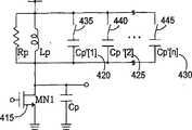
Fig. 4 (b) is example according to the present invention, with the general version of circuit diagram key diagram 3 (a), can use a single driving transistors MN1 to carry out Multiband-operation.
Embodiment
The preferred embodiments according to the present invention will illustrate a kind of gain control method and device that is used for low noise amplifier (as tuner) and preamplifier in wireless telecommunication system.For example, a preferred embodiments of gain control method and device is applicable to the circuit design of wireless terminal, and implements in a LNA or preamplifier.But the present invention is not limited thereto.The present invention also can be applicable to the device industrial technology of any kind in addition, as bipolar joint transistor (BJT) or in conjunction with field-effect transistor (JFET) etc.For illustration purpose, below will illustrate according to preferred embodiments of the present invention, wherein use metal oxide semiconductcor field effect transistor (MOSFET) industrial technology.
Fig. 2 (a) is described in Figure a preferred embodiments of amplifier according to the present invention, and Fig. 2 (a) illustrates a tuning LNA, and it has the gain of wanting in a narrow-band.LNA can load construction by n-channel MOS (NMOS) transistor MN1 200 and and form, and wherein this loading comprises a capacitor Cp 205, an inductor Lp 210 and a resistor R p 215.Can apply an input signal at the gate node of common source nmos pass transistor (MN1) 200, and its amplifying signal occur or so far be coupled an outlet terminal 214 at drain node 212.Preferably resistor R p 215 and inductor Lp 210 are coupling between this power supply supply voltage 216 (for example Vdd) and this drain node 212, and capacitor Cp 205 is coupling between this earth terminal 218 and this drain node 212.Capacitor Cp 205 can help to form the input capacitance of next stage (as blender), and/or the parasitic capacitance on the output node.Inductor Lp 210 preferably forms a resonant circuit in parallel with capacitor Cp 205, and with the frequency that the gain tuning to of LNA is wanted, this gain peak is positioned on the resonance frequency.Can use a spiral or overlap joint line inductor (or by using an external inductance) to implement inductor Lp 210.According to an example of the present invention, for the suitably gain of control LNA, and avoid input signal (by saturated or cut-out) to make its output distortion, resistor R p 215 is variable.In order to reduce the gain of the input signal that value increases, reducing the drain bias electric current (is i among Fig. 2 (a)
DThe direct current spare part) but power saving but may cause the line style deterioration by undesired MN1 200 rupturing operations.Yet,, do not influence the line style of LNA for reducing the value that gain reduces Rp 215 among Fig. 2 (a).Therefore, if line style than reducing the prior words of power consumption, in order to change gain, may command Rp 215 but not control drain bias electric current.Gain with at the Rp of resonance frequency
2Proportional, therefore, because the quality factor Q that resonance loads is direct and Rp 215 is proportional, for the fixed value of Cp 205 and Lp 210, the quality factor Q2 also proportional (promptly proportional) of gain and resonant circuit with the acutance of gain peak:
Therefore, for the fixed value of Cp 205 and Lp 210, control Rp 215 equals to control Q.
The preferred embodiments that Fig. 2 (b) key diagram 2 (a) amplifier circuit is implemented, a variable resistance or a variable resistor shown in Fig. 2 (b) are with the straight p channel of parallel connection MOS (PMOS) transistor MP[1]~MP[n] (220,225,230) enforcement.Make each PMOS transistor (when its lock pressure drop is low) when connecting, in its linear areas, operate, so can shown in Fig. 2 (c), it be used as one have the switch of connecting resistance.By signal ctrl[1]~ctrl[n] (235,240 ... 245) this clean resistance of logic control.By one by one controlling these PMOS switches, can adjust amplifier gain gradually.When all connecting, amplifier has least gain when these PMOS switches (by reducing its whole lock voltages).
Add a common gate nmos pass transistor MC1 250, with further isolation input and output, to lower Miller effect.Bias voltage produces block BIAS GEN1 255 by MC1 250 is maintained the zone of saturation, makes the operation of MC1 250 not be subjected to or be subjected to less the swing of output signal to influence.
The Q that reduces this loading is really than reducing the less deterioration line style of direct current bias current, but higher than other method power consumption.In order to keep the circuit line style of Fig. 2 (b), must keep the drain bias electric current, and follow certain direct current power consumption.Because the conduction parameter k (proportional with grid width) of MN1 200 fixes the circuit among Fig. 2 (b), so can not reduce the direct current power consumption of amplifier.If reduce the direct current power consumption, just need new gain control method.
In order to reduce power consumption, can use among Fig. 3 (a) circuit of preferred embodiments according to the present invention by k can be changed.Shown in Fig. 3 (a), this driving transistors MN1 200 is divided into separately nmos pass transistor MN[1]~MN[n] (as 300,305 ... 310).These transistors are by corresponding nmos pass transistor MC[1]~MC[n] (as 315,320,325) controlled, in Fig. 3 (b) also with the example explanation, distinctly by its corresponding PMOS switch 330,335 ... 340 connect and close these corresponding nmos pass transistors.When the value of output increases, can preferably increase the grid bias that has BIAS_GEN2 345 signals among Fig. 3 (a), to keep line style.In order to reduce gain simultaneously and to reduce the direct current power consumption, can be preferably with than increase grid bias faster ratio reduce the k value.Add broad gap because the quick change of k can cause the gain ladder herein, must between the smoothness of power consumption minimizing and gain controlling, seek a balance.Pull-up resistance (Rp) 350 is variable as Rp 215 if preferably make, and then obtains gain controlling more stably.In one example, the p channel MOS (PMOS) among available Fig. 2 (b) implements this variable resistor.
The circuit of Fig. 3 (a) also can be in wireless terminal unit as the preamplifier of a reflector; But in this case, must place a low capacity in its output loads.This is that the input impedance of this power amplifier can be set at 50 Ω (normal impedance in the microwave engineering) because of a typical preamplifier driving power amplifier.
Shown in Fig. 4 (a), a pull-up capacitor Cp ' 400 can be in parallel with pull-up inductor Lp 410, and connected and closed by its tandem tap 405.To this example of the present invention, implement switch 405 and can replenish a MOSFET (CMOS) " transmission gate ", on so can proportionately resonance frequency being moved down and be moved.If amplifier in another converted band stable operation, then can make resonance frequency drop on another frequency band of wanting.The example of biobelt operation can be the amplifier of wireless telecommunications, and the frequency band that can be used for mobile phone is about 800MHZ, is used for PCS person and is about 1800MHZ (for TCM).Can choose the frequency band of wanting by an external signal of control cmos switch.Can finish additional band by the circuit of execution graph 4 (b) and choose, wherein the circuit of Fig. 4 (b) is another preferred embodiments of Fig. 4 (a) circuit.The preferred embodiments of Fig. 4 (b) can be finished many ribbon gymnastics with a single driving transistors MN1 415 and do.In the operation, can by the tandem tap of correspondence (as 435,440 ... 445) (as cmos transmission gate switch and so on) individually or jointly connect and close capacitor Cp ' [1]-Cp ' [n] (as 420,425 ... 430).
As above-mentioned, in wireless telecommunications, be used for the method for gain controlling and the preferred embodiments of device and have multiple advantage, for fear of an integrated preamplifier or use the distortion of being obstructed of the output signal of the low noise amplifier of MOSFET technology (as the terminal unit of wireless telecommunications), according to these preferred embodiments, can and use a variable resistance in pull-up loads, and the order gain becomes adjustable.Can be shown in Fig. 2 (b), use the PMOS transistor of implementing at linear zone that separates and operate this variable resistance.For obtaining the controllability of gain, and the controllability of direct current power consumption, in a preferred embodiments, also a driving transistors can be divided into a plurality of separately transistors that can connect individually and close.In addition, in a preferred embodiments, select an extra capacitor or its analog and a load inductor parallel coupled can be adjusted a resonance frequency and/or carried out multi-band operation.
Above example and advantage are example only, are not in order to restriction the present invention.This teachings can be applied to the device of other type easily.Explanation of the present invention only is used to describe it, is not the scope in order to restriction claims.Those skilled in the art can do many selections, improvement and variation.In claims, device adds that the description of function contains as herein describedly as the structure of carrying out recited function, non-ly only contains equivalent structures, and also contains equivalent structure.
Claims (22)
1. variable gain amplifier comprises:
One the first transistor has a control electrode, one first electrode and one second electrode, wherein an input signal is coupled to this control electrode, and one is coupled to first reference voltage of first electrode, and an output signal that is coupled to second electrode;
One load inductor, it is coupling between second electrode of one second reference voltage and this first transistor;
One is coupled to the load capacitor of second electrode of this first transistor; And
One parallel connection is coupled to the variable resistance of load inductor.
2. variable amplifier according to claim 1, wherein this variable resistance comprises at least one transistor AND gate load inductor parallel connection, and is coupled to a control circuit network.
3. variable gain amplifier according to claim 1 comprises that also one is coupling in second electrode of the first transistor and the isolated transistor between the load capacitor.
4. variable gain amplifier according to claim 1 also comprises a plurality of transistor secondses, and these transistor secondses are coupled to first network on corresponding gate control lines road, wherein each transistor seconds is coupled in parallel to this first transistor.
5. variable gain amplifier according to claim 4 also comprises a plurality of the 3rd transistors, is coupling in separately between these first and second transistorized corresponding second electrode and the load capacitor.
6. variable gain amplifier according to claim 5 is wherein with second network of these grade in an imperial examination three transistors couple to corresponding gate control lines road.
7. variable gain amplifier according to claim 1 also comprises at least one the pull-up capacitor that is coupled in parallel to load inductor.
8. variable gain amplifier according to claim 1, also comprise a plurality of pull-up capacitors that are coupled in parallel to load inductor, wherein the pull-up capacitor can independently be selected by a plurality of switches, and each switch makes a corresponding pull-up capacitor and load inductor coupling.
9. variable gain amplifier according to claim 8 is wherein implemented these switches in CMOS skill.
10. variable gain amplifier according to claim 8, wherein according to the selection of pull-up capacitor, and load resistance and the load inductance of choosing a pull-up capacitor and a variable resistance form a resonant circuit.
11. variable gain amplifier according to claim 10, wherein this circuit is at 800 megahertzes (MHz) or 1800 megahertz resonance.
12. variable gain amplifier according to claim 6, wherein variable resistor comprises a plurality of load transistors that are coupled in parallel to load inductor, and wherein each load transistor has a corresponding network of a gate coupled to the 3rd control circuit network.
13. variable gain amplifier according to claim 12, also comprise a plurality of pull-up capacitors that are coupled in parallel to load inductor, wherein these pull-up capacitors are independently chosen by a plurality of switches, and each switch makes corresponding pull-up capacitor and the coupling of this load inductor.
14. variable gain amplifier according to claim 12 also comprises:
A plurality of transistor secondses are coupled to one first corresponding gate control lines road network network, wherein each transistor seconds are coupled in parallel to the first transistor;
A plurality of the 3rd transistors are coupling between corresponding second electrode and this load capacitor of these first and second transistors, wherein with the 3rd transistors couple to the one second corresponding gate control lines road network network; And
One isolated transistor is coupling between second electrode and this load capacitor of this first transistor.
15. variable gain amplifier according to claim 14, also comprise a plurality of pull-up capacitors that are coupled in parallel to load inductor, wherein the pull-up capacitor is independently chosen by a plurality of switches, and each switch makes pull-type capacitor and the coupling of this load inductor on the correspondence.
16. a multifrequency amplifier comprises:
One driving transistors has one source pole, grid and drain electrode, wherein imports an input signal by the input that is coupled to grid, with source-coupled to a reference voltage source, and exports an output signal by the output that is coupled to drain electrode;
One load inductor is coupling between a voltage source and the output;
One load capacitor is coupling between output and the reference voltage source;
One variable resistance is coupling in voltage source and is connected in parallel between the output of load inductor; And
At least one pull-up capacitor, use in parallel with load inductor, wherein this at least one pull-up capacitor is independently chosen by a plurality of switches, and each switch makes this at least one capacitor and the coupling of this load inductor.
17. multifrequency amplifier according to claim 16 also comprises an isolated transistor, is coupling between the drain electrode and this load capacitor of driving transistors.
18. multifrequency amplifier according to claim 16 also comprises:
A plurality of additional drives transistors, each is coupled in parallel to driving transistors, and wherein the grid of driving transistors receives a variable bias; And
A plurality of isolated transistors are coupling between the drain electrode and load capacitor of driving transistors, wherein optionally a plurality of isolated transistors are coupled to a gate control lines road network network.
19. multifrequency amplifier according to claim 18, wherein variable resistance comprises a plurality of load transistors that are coupled in parallel to load inductor, and wherein each load transistor has an one of gate coupled to the 3rd control circuit network map network.
20. multifrequency amplifier according to claim 16, wherein variable resistance comprises a plurality of load transistors that are coupled in parallel to load inductor, and wherein each load transistor has an one of gate coupled to the 3rd control circuit network map network.
21. multifrequency amplifier according to claim 16 wherein according to the selection of pull-up capacitor, forms a resonant circuit and choose pull-up capacitor and load resistance and load inductance.
22. multifrequency amplifier according to claim 19, wherein circuit is at 800 megahertzes (MHz) or 1800 megahertz resonance, and wherein implements these switches in CMOS skill.
Applications Claiming Priority (5)
| Application Number | Priority Date | Filing Date | Title |
|---|---|---|---|
| US27945101P | 2001-03-29 | 2001-03-29 | |
| US60/279,451 | 2001-03-29 | ||
| US09/940,806 | 2001-08-29 | ||
| US09/940,806 US6424222B1 (en) | 2001-03-29 | 2001-08-29 | Variable gain low noise amplifier for a wireless terminal |
| PCT/US2002/009478 WO2002080357A1 (en) | 2001-03-29 | 2002-03-28 | Variable gain low-noise amplifier for a wireless terminal |
Publications (2)
| Publication Number | Publication Date |
|---|---|
| CN1502164A true CN1502164A (en) | 2004-06-02 |
| CN1315255C CN1315255C (en) | 2007-05-09 |
Family
ID=26959667
Family Applications (1)
| Application Number | Title | Priority Date | Filing Date |
|---|---|---|---|
| CNB028075145A Expired - Lifetime CN1315255C (en) | 2001-03-29 | 2002-03-28 | Variable gain low-noise amplifier for a wireless terminal |
Country Status (11)
| Country | Link |
|---|---|
| US (2) | US6424222B1 (en) |
| EP (1) | EP1374396B1 (en) |
| JP (1) | JP2004522350A (en) |
| KR (1) | KR100914730B1 (en) |
| CN (1) | CN1315255C (en) |
| AT (1) | ATE431009T1 (en) |
| CA (1) | CA2442332A1 (en) |
| DE (1) | DE60232230D1 (en) |
| HK (1) | HK1064813A1 (en) |
| TW (1) | TWI286878B (en) |
| WO (1) | WO2002080357A1 (en) |
Cited By (5)
| Publication number | Priority date | Publication date | Assignee | Title |
|---|---|---|---|---|
| CN1841923B (en) * | 2005-03-29 | 2010-09-08 | 因特格瑞特科技有限公司 | Low noise amplifier and differential amplifier with variable gain mode |
| CN103095330A (en) * | 2011-10-28 | 2013-05-08 | 美国博通公司 | Dual mode local area network transceiver and methods for use therewith |
| CN103138725A (en) * | 2013-01-11 | 2013-06-05 | 华为技术有限公司 | Circuit with metal board capacitor, ratio frequency switch with metal board capacitor and low-noise amplifier |
| CN105680803A (en) * | 2014-12-05 | 2016-06-15 | 英飞凌科技股份有限公司 | System and method for low noise amplifier module |
| WO2020199065A1 (en) * | 2019-03-30 | 2020-10-08 | 华为技术有限公司 | Variable gain amplifier and phased array transceiver |
Families Citing this family (70)
| Publication number | Priority date | Publication date | Assignee | Title |
|---|---|---|---|---|
| US6621348B2 (en) * | 2001-10-25 | 2003-09-16 | Motorola, Inc. | Variable gain amplifier with autobiasing supply regulation |
| US7113033B2 (en) * | 2002-01-31 | 2006-09-26 | Qualcomm Incorporated | Variable impedance load for a variable gain radio frequency amplifier |
| US6639472B2 (en) * | 2002-03-26 | 2003-10-28 | Intel Corporation | High bandwidth, low power, single stage cascode transimpedance amplifier for short haul optical links |
| GB2410141B (en) * | 2002-07-24 | 2006-03-15 | Sirific Wireless Corp | Multi-standard amplifier |
| US7010330B1 (en) | 2003-03-01 | 2006-03-07 | Theta Microelectronics, Inc. | Power dissipation reduction in wireless transceivers |
| JP3906173B2 (en) * | 2003-03-17 | 2007-04-18 | 松下電器産業株式会社 | Variable gain amplifier circuit |
| US6819179B2 (en) * | 2003-04-16 | 2004-11-16 | Agency For Science, Technology And Research | Variable gain low noise amplifier |
| US6888411B2 (en) * | 2003-06-06 | 2005-05-03 | Broadcom Corporation | Radio frequency variable gain amplifier with linearity insensitive to gain |
| JP2005033596A (en) | 2003-07-08 | 2005-02-03 | Nec Corp | High-frequency amplifying circuit |
| US7173489B1 (en) * | 2003-08-25 | 2007-02-06 | Marvell Semiconductor, Inc. | Programmable gain voltage buffer |
| JP4176606B2 (en) * | 2003-09-29 | 2008-11-05 | シャープ株式会社 | High frequency receiver using grounded emitter circuit. |
| CN100442656C (en) * | 2003-10-21 | 2008-12-10 | 瑞昱半导体股份有限公司 | low noise amplifier and method for amplifying signal |
| JP2005167501A (en) * | 2003-12-01 | 2005-06-23 | Sanyo Electric Co Ltd | Tuning circuit with amplitude attenuation function and integrated circuit for wireless communication device |
| US9026070B2 (en) | 2003-12-18 | 2015-05-05 | Qualcomm Incorporated | Low-power wireless diversity receiver with multiple receive paths |
| US7023272B2 (en) * | 2004-04-19 | 2006-04-04 | Texas Instruments Incorporated | Multi-band low noise amplifier system |
| DE102004021153B3 (en) * | 2004-04-29 | 2005-09-15 | Infineon Technologies Ag | Ultra-wideband signal amplifier for radio receiver uses tunable narrow band amplifier connected to frequency control circuit with store for sequence of chosen bands |
| JP2006072817A (en) * | 2004-09-03 | 2006-03-16 | Koito Mfg Co Ltd | Peak detection circuit and discharge lamp lighting device |
| US7084707B2 (en) * | 2004-09-24 | 2006-08-01 | Realtek Semiconductor Corp. | Low noise amplifier and related method |
| KR100877504B1 (en) * | 2005-07-07 | 2009-01-07 | 삼성전자주식회사 | Apparatus and Method for Reducing Drain Modulation of High Power Transistors |
| US7834704B2 (en) * | 2005-08-30 | 2010-11-16 | Panasonic Corporation | Low-noise amplifier circuit and receiving system |
| US9450665B2 (en) | 2005-10-19 | 2016-09-20 | Qualcomm Incorporated | Diversity receiver for wireless communication |
| JP2007189569A (en) * | 2006-01-16 | 2007-07-26 | Ricoh Co Ltd | Amplifier, and radio communication apparatus using it |
| KR100709326B1 (en) | 2006-09-26 | 2007-04-20 | 삼성전자주식회사 | Variable Gain Amplifier |
| JP2010512538A (en) | 2006-12-11 | 2010-04-22 | クエーサー・フェデラル・システムズ・インコーポレーテッド | Small underwater electromagnetic measurement system |
| US7689187B2 (en) * | 2007-03-01 | 2010-03-30 | Motorola, Inc. | Dual input low noise amplifier for multi-band operation |
| JP2008277882A (en) * | 2007-04-25 | 2008-11-13 | Matsushita Electric Ind Co Ltd | Amplifying circuit and radio communication device |
| US7486135B2 (en) * | 2007-05-29 | 2009-02-03 | Telefonaktiebolaget Lm Ericsson (Publ) | Configurable, variable gain LNA for multi-band RF receiver |
| JP2009065511A (en) * | 2007-09-07 | 2009-03-26 | Fujitsu Ltd | Amplifier circuit and communication device |
| US7701289B2 (en) * | 2007-10-24 | 2010-04-20 | Industrial Technology Research Institute | Variable gain amplifier including series-coupled cascode amplifiers |
| US7760019B2 (en) * | 2008-03-04 | 2010-07-20 | Micron Technology, Inc. | Adaptive operational transconductance amplifier load compensation |
| US8229043B2 (en) * | 2008-03-21 | 2012-07-24 | Qualcomm Incorporated | Stepped gain mixer |
| WO2009137522A2 (en) * | 2008-05-06 | 2009-11-12 | Rambus Inc. | Method and apparatus for power sequence timing to mitigate supply resonance in power distribution network |
| US8571510B2 (en) * | 2008-08-18 | 2013-10-29 | Qualcomm Incorporated | High linearity low noise receiver with load switching |
| JP4903834B2 (en) * | 2009-04-27 | 2012-03-28 | 株式会社日立製作所 | Variable gain amplifier circuit and integrated circuit for wireless communication equipment using the same |
| JP5308243B2 (en) * | 2009-06-10 | 2013-10-09 | 株式会社日立製作所 | Variable gain circuit |
| WO2011023210A1 (en) * | 2009-08-27 | 2011-03-03 | Verigy ( Singapore) Pte. Ltd. | Adjustable gain amplifier, automated test equipment and method for adjusting a gain of an amplifier |
| JP2011055055A (en) * | 2009-08-31 | 2011-03-17 | Texas Instr Japan Ltd | Amplifier circuit, signal strength detection circuit, and offset voltage adjustment method |
| TWM377794U (en) * | 2009-09-18 | 2010-04-01 | Princeton Technology Corp | Low noise amplifier and radio frequency signal receiving system |
| JPWO2011111140A1 (en) * | 2010-03-10 | 2013-06-27 | パナソニック株式会社 | Variable gain amplifier |
| US8912843B2 (en) * | 2010-07-06 | 2014-12-16 | Cadence Ams Design India Private Limited | Ultra low cut-off frequency filter |
| US8258869B2 (en) * | 2010-08-01 | 2012-09-04 | Quintic Holdings | Low noise amplifier with current bleeding branch |
| US9178669B2 (en) | 2011-05-17 | 2015-11-03 | Qualcomm Incorporated | Non-adjacent carrier aggregation architecture |
| US9252827B2 (en) | 2011-06-27 | 2016-02-02 | Qualcomm Incorporated | Signal splitting carrier aggregation receiver architecture |
| US9154179B2 (en) | 2011-06-29 | 2015-10-06 | Qualcomm Incorporated | Receiver with bypass mode for improved sensitivity |
| US12081243B2 (en) | 2011-08-16 | 2024-09-03 | Qualcomm Incorporated | Low noise amplifiers with combined outputs |
| US20130109331A1 (en) * | 2011-10-28 | 2013-05-02 | Broadcom Corporation | Transmit/receive switch with esd protection and methods for use therewith |
| US8400224B1 (en) * | 2011-10-28 | 2013-03-19 | Broadcom Corporation | Programmable low noise amplifier and methods for use therewith |
| US8774334B2 (en) | 2011-11-09 | 2014-07-08 | Qualcomm Incorporated | Dynamic receiver switching |
| US9362958B2 (en) | 2012-03-02 | 2016-06-07 | Qualcomm Incorporated | Single chip signal splitting carrier aggregation receiver architecture |
| US9172402B2 (en) | 2012-03-02 | 2015-10-27 | Qualcomm Incorporated | Multiple-input and multiple-output carrier aggregation receiver reuse architecture |
| US9118439B2 (en) | 2012-04-06 | 2015-08-25 | Qualcomm Incorporated | Receiver for imbalanced carriers |
| US9154356B2 (en) | 2012-05-25 | 2015-10-06 | Qualcomm Incorporated | Low noise amplifiers for carrier aggregation |
| US9867194B2 (en) | 2012-06-12 | 2018-01-09 | Qualcomm Incorporated | Dynamic UE scheduling with shared antenna and carrier aggregation |
| CN102790589B (en) * | 2012-08-27 | 2015-04-29 | 上海市计量测试技术研究院 | Amplifier for measuring 1MHz common mode rejection ratios of high-resistance high-voltage differential probe |
| US9300420B2 (en) | 2012-09-11 | 2016-03-29 | Qualcomm Incorporated | Carrier aggregation receiver architecture |
| US9543903B2 (en) | 2012-10-22 | 2017-01-10 | Qualcomm Incorporated | Amplifiers with noise splitting |
| US8995591B2 (en) | 2013-03-14 | 2015-03-31 | Qualcomm, Incorporated | Reusing a single-chip carrier aggregation receiver to support non-cellular diversity |
| US8970296B1 (en) | 2013-03-26 | 2015-03-03 | Guerrilla RF, Inc. | Amplifying circuit with bypass mode and series isolation switch |
| CN105379110B (en) * | 2013-08-08 | 2018-01-05 | 株式会社索思未来 | Antiresonant circuit |
| US9979388B2 (en) * | 2013-11-07 | 2018-05-22 | Nxp Usa, Inc. | Adjustable losses of bond wire arrangement |
| US10177722B2 (en) | 2016-01-12 | 2019-01-08 | Qualcomm Incorporated | Carrier aggregation low-noise amplifier with tunable integrated power splitter |
| JP6470213B2 (en) * | 2016-03-16 | 2019-02-13 | 日本電信電話株式会社 | Variable gain amplifier |
| JP6845461B2 (en) * | 2016-07-28 | 2021-03-17 | 株式会社村田製作所 | Amplifier circuit |
| US12040757B2 (en) | 2018-10-03 | 2024-07-16 | Richwave Technology Corp. | Amplifier circuit |
| TWI672903B (en) | 2018-10-03 | 2019-09-21 | 立積電子股份有限公司 | Amplifier circuit |
| CN109787574B (en) * | 2018-12-29 | 2021-05-04 | 南京汇君半导体科技有限公司 | Millimeter wave variable gain amplifier structure |
| US11515841B2 (en) * | 2019-05-31 | 2022-11-29 | Macom Technology Solutions Holdings, Inc. | DC coupled amplifier having pre-driver and bias control |
| EP4038309A4 (en) * | 2019-10-04 | 2024-04-03 | Versitech Limited | Current-limiting driver circuit and method |
| TWI819309B (en) * | 2021-05-25 | 2023-10-21 | 立積電子股份有限公司 | Radio frequency amplifier and bias circuit |
| US20230387868A1 (en) * | 2022-05-25 | 2023-11-30 | Qualcomm Incorporated | Wideband Amplifier |
Family Cites Families (18)
| Publication number | Priority date | Publication date | Assignee | Title |
|---|---|---|---|---|
| US3191127A (en) * | 1962-04-02 | 1965-06-22 | Rca Corp | Agc with compensation for change in collector capacitance |
| US3559088A (en) * | 1969-08-07 | 1971-01-26 | Motorola Inc | Transistor amplifier with automatic gain control |
| US4520324A (en) * | 1983-03-11 | 1985-05-28 | National Semiconductor Corporation | MOS Gain controlled amplifier |
| US4586004A (en) * | 1983-06-27 | 1986-04-29 | Saber Technology Corp. | Logic and amplifier cells |
| FR2558997B1 (en) * | 1984-01-31 | 1989-02-03 | Thomson Csf | ELECTRIC SIGNAL GROUP PROPAGATION TIME CORRECTING AMPLIFIER AND INTERFERENCE FREQUENCY AMPLIFICATION CHAIN OF RADIO BEAMS INCLUDING SUCH AMPLIFIER |
| JP2938999B2 (en) * | 1991-05-23 | 1999-08-25 | 松下電器産業株式会社 | Semiconductor device for tuner and tuner |
| US5355096A (en) * | 1993-07-06 | 1994-10-11 | Trw Inc. | Compace HBT wide band microwave variable gain active feedback amplifier |
| JPH07106907A (en) * | 1993-10-04 | 1995-04-21 | Alps Electric Co Ltd | High frequency band amplifier |
| DE4341507C1 (en) * | 1993-12-06 | 1995-02-23 | Siemens Ag | Amplifier stage |
| JP2685014B2 (en) * | 1995-02-28 | 1997-12-03 | 日本電気株式会社 | High frequency amplifier |
| JPH09298477A (en) * | 1995-06-29 | 1997-11-18 | Sony Corp | Short wave receiver and low-pass filter |
| JPH10190378A (en) * | 1996-12-27 | 1998-07-21 | Nec Corp | Super highly efficient linear amplifier |
| FR2770053B1 (en) * | 1997-10-22 | 2000-01-07 | Sgs Thomson Microelectronics | DOUBLE GAIN AMPLIFIER CIRCUIT |
| JP2000036564A (en) * | 1998-07-21 | 2000-02-02 | Oki Electric Ind Co Ltd | Variable resistor and gain circuit |
| JP2000101360A (en) * | 1998-09-21 | 2000-04-07 | Sanyo Electric Co Ltd | Amplifier |
| US6100761A (en) * | 1998-10-07 | 2000-08-08 | Microtune, Inc. | Highly linear variable-gain low noise amplifier |
| JP2000261265A (en) * | 1999-03-10 | 2000-09-22 | Toshiba Microelectronics Corp | Feedback type variable gain amplification circuit |
| GB9916901D0 (en) * | 1999-07-19 | 1999-09-22 | Cambridge Silicon Radio Ltd | Adjustable filter |
-
2001
- 2001-08-29 US US09/940,806 patent/US6424222B1/en not_active Expired - Lifetime
-
2002
- 2002-03-28 WO PCT/US2002/009478 patent/WO2002080357A1/en active Application Filing
- 2002-03-28 KR KR1020037012747A patent/KR100914730B1/en active IP Right Grant
- 2002-03-28 EP EP02757825A patent/EP1374396B1/en not_active Expired - Lifetime
- 2002-03-28 CA CA002442332A patent/CA2442332A1/en not_active Abandoned
- 2002-03-28 AT AT02757825T patent/ATE431009T1/en not_active IP Right Cessation
- 2002-03-28 JP JP2002578645A patent/JP2004522350A/en active Pending
- 2002-03-28 CN CNB028075145A patent/CN1315255C/en not_active Expired - Lifetime
- 2002-03-28 DE DE60232230T patent/DE60232230D1/en not_active Expired - Fee Related
- 2002-03-29 TW TW091106312A patent/TWI286878B/en not_active IP Right Cessation
- 2002-07-17 US US10/196,136 patent/US6657498B2/en not_active Expired - Lifetime
-
2004
- 2004-09-27 HK HK04107455A patent/HK1064813A1/en not_active IP Right Cessation
Cited By (7)
| Publication number | Priority date | Publication date | Assignee | Title |
|---|---|---|---|---|
| CN1841923B (en) * | 2005-03-29 | 2010-09-08 | 因特格瑞特科技有限公司 | Low noise amplifier and differential amplifier with variable gain mode |
| CN103095330A (en) * | 2011-10-28 | 2013-05-08 | 美国博通公司 | Dual mode local area network transceiver and methods for use therewith |
| CN103138725A (en) * | 2013-01-11 | 2013-06-05 | 华为技术有限公司 | Circuit with metal board capacitor, ratio frequency switch with metal board capacitor and low-noise amplifier |
| CN105680803A (en) * | 2014-12-05 | 2016-06-15 | 英飞凌科技股份有限公司 | System and method for low noise amplifier module |
| CN105680803B (en) * | 2014-12-05 | 2019-05-10 | 英飞凌科技股份有限公司 | Systems and methods for low noise amplifier modules |
| WO2020199065A1 (en) * | 2019-03-30 | 2020-10-08 | 华为技术有限公司 | Variable gain amplifier and phased array transceiver |
| US12119797B2 (en) | 2019-03-30 | 2024-10-15 | Huawei Technologies Co., Ltd. | Variable gain amplifier and phased array transceiver |
Also Published As
| Publication number | Publication date |
|---|---|
| KR100914730B1 (en) | 2009-08-31 |
| ATE431009T1 (en) | 2009-05-15 |
| EP1374396A4 (en) | 2007-12-12 |
| CN1315255C (en) | 2007-05-09 |
| EP1374396B1 (en) | 2009-05-06 |
| US20020190796A1 (en) | 2002-12-19 |
| HK1064813A1 (en) | 2005-02-04 |
| WO2002080357A1 (en) | 2002-10-10 |
| US6657498B2 (en) | 2003-12-02 |
| JP2004522350A (en) | 2004-07-22 |
| CA2442332A1 (en) | 2002-10-10 |
| DE60232230D1 (en) | 2009-06-18 |
| TWI286878B (en) | 2007-09-11 |
| EP1374396A1 (en) | 2004-01-02 |
| KR20040015080A (en) | 2004-02-18 |
| US6424222B1 (en) | 2002-07-23 |
Similar Documents
| Publication | Publication Date | Title |
|---|---|---|
| CN1315255C (en) | Variable gain low-noise amplifier for a wireless terminal | |
| US7486135B2 (en) | Configurable, variable gain LNA for multi-band RF receiver | |
| KR100952666B1 (en) | Reconfigurable Low Noise Amplifier with Capacitor Feedback | |
| US5517688A (en) | MMIC FET mixer and method | |
| US6850753B2 (en) | Tunable low noise amplifier and current-reused mixer for a low power RF application | |
| US7512389B2 (en) | Active inductors using bipolar silicon transistors | |
| US20230108382A1 (en) | Dual-band low-noise amplifier circuit, low-noise amplifier, and device | |
| US6181206B1 (en) | Low noise RF amplifier with programmable gain | |
| JP2008545336A (en) | Two-stage microwave class E power amplifier | |
| KR20010053413A (en) | Mobile telephone system | |
| US7626459B2 (en) | High frequency amplifier circuit and mobile communication terminal using the same | |
| US20020102971A1 (en) | Scheme for maximizing efficiency of power amplifier under power backoff conditions | |
| US6630861B2 (en) | Variable gain amplifier | |
| CN1182747C (en) | Circuits for Efficient Generation of Low Power RF Signals | |
| EP0696870B1 (en) | Double tuned and band-switchable RF circuit with balanced output signals | |
| EP2045913A1 (en) | Low noise amplifier and N-mode gain control circuit therefor | |
| KR100415408B1 (en) | High-freguency switch circuit suppressing the distortion of high freguency signal | |
| US6753736B2 (en) | Amplifier circuit for AM broadcasting | |
| US7299028B2 (en) | Low power, low noise figure, latch driver circuit | |
| US20080297262A1 (en) | Increased gain high-frequency amplifier | |
| Lian et al. | A dual-band LNA with 0.18-μm CMOS switches | |
| EP1309083A1 (en) | Method for switching the gain of an amplifier and a switched gain low noise amplifier | |
| CN112491437A (en) | Radio frequency front-end circuit with multiple antenna modes and integrated circuit module | |
| Morkner et al. | A 1.7 mA low noise amplifier with integrated bypass switch for wireless 0.05-6 GHz portable applications |
Legal Events
| Date | Code | Title | Description |
|---|---|---|---|
| C06 | Publication | ||
| PB01 | Publication | ||
| C10 | Entry into substantive examination | ||
| SE01 | Entry into force of request for substantive examination | ||
| REG | Reference to a national code |
Ref country code: HK Ref legal event code: DE Ref document number: 1064813 Country of ref document: HK |
|
| C14 | Grant of patent or utility model | ||
| GR01 | Patent grant | ||
| CX01 | Expiry of patent term | ||
| CX01 | Expiry of patent term |
Granted publication date: 20070509 |