CN1426269A - Display device and its producing method - Google Patents
Display device and its producing method Download PDFInfo
- Publication number
- CN1426269A CN1426269A CN02154005A CN02154005A CN1426269A CN 1426269 A CN1426269 A CN 1426269A CN 02154005 A CN02154005 A CN 02154005A CN 02154005 A CN02154005 A CN 02154005A CN 1426269 A CN1426269 A CN 1426269A
- Authority
- CN
- China
- Prior art keywords
- color filter
- red
- green
- organic
- electrode
- Prior art date
- Legal status (The legal status is an assumption and is not a legal conclusion. Google has not performed a legal analysis and makes no representation as to the accuracy of the status listed.)
- Granted
Links
Images


Classifications
-
- H—ELECTRICITY
- H05—ELECTRIC TECHNIQUES NOT OTHERWISE PROVIDED FOR
- H05B—ELECTRIC HEATING; ELECTRIC LIGHT SOURCES NOT OTHERWISE PROVIDED FOR; CIRCUIT ARRANGEMENTS FOR ELECTRIC LIGHT SOURCES, IN GENERAL
- H05B33/00—Electroluminescent light sources
- H05B33/12—Light sources with substantially two-dimensional radiating surfaces
- H05B33/22—Light sources with substantially two-dimensional radiating surfaces characterised by the chemical or physical composition or the arrangement of auxiliary dielectric or reflective layers
-
- H—ELECTRICITY
- H10—SEMICONDUCTOR DEVICES; ELECTRIC SOLID-STATE DEVICES NOT OTHERWISE PROVIDED FOR
- H10K—ORGANIC ELECTRIC SOLID-STATE DEVICES
- H10K59/00—Integrated devices, or assemblies of multiple devices, comprising at least one organic light-emitting element covered by group H10K50/00
- H10K59/30—Devices specially adapted for multicolour light emission
- H10K59/38—Devices specially adapted for multicolour light emission comprising colour filters or colour changing media [CCM]
-
- H—ELECTRICITY
- H10—SEMICONDUCTOR DEVICES; ELECTRIC SOLID-STATE DEVICES NOT OTHERWISE PROVIDED FOR
- H10K—ORGANIC ELECTRIC SOLID-STATE DEVICES
- H10K50/00—Organic light-emitting devices
- H10K50/80—Constructional details
- H10K50/86—Arrangements for improving contrast, e.g. preventing reflection of ambient light
- H10K50/865—Arrangements for improving contrast, e.g. preventing reflection of ambient light comprising light absorbing layers, e.g. light-blocking layers
-
- H—ELECTRICITY
- H10—SEMICONDUCTOR DEVICES; ELECTRIC SOLID-STATE DEVICES NOT OTHERWISE PROVIDED FOR
- H10K—ORGANIC ELECTRIC SOLID-STATE DEVICES
- H10K59/00—Integrated devices, or assemblies of multiple devices, comprising at least one organic light-emitting element covered by group H10K50/00
- H10K59/80—Constructional details
- H10K59/87—Passivation; Containers; Encapsulations
- H10K59/871—Self-supporting sealing arrangements
-
- H—ELECTRICITY
- H10—SEMICONDUCTOR DEVICES; ELECTRIC SOLID-STATE DEVICES NOT OTHERWISE PROVIDED FOR
- H10K—ORGANIC ELECTRIC SOLID-STATE DEVICES
- H10K59/00—Integrated devices, or assemblies of multiple devices, comprising at least one organic light-emitting element covered by group H10K50/00
- H10K59/80—Constructional details
- H10K59/8791—Arrangements for improving contrast, e.g. preventing reflection of ambient light
- H10K59/8792—Arrangements for improving contrast, e.g. preventing reflection of ambient light comprising light absorbing layers, e.g. black layers
-
- H—ELECTRICITY
- H10—SEMICONDUCTOR DEVICES; ELECTRIC SOLID-STATE DEVICES NOT OTHERWISE PROVIDED FOR
- H10K—ORGANIC ELECTRIC SOLID-STATE DEVICES
- H10K2102/00—Constructional details relating to the organic devices covered by this subclass
- H10K2102/301—Details of OLEDs
- H10K2102/302—Details of OLEDs of OLED structures
- H10K2102/3023—Direction of light emission
- H10K2102/3026—Top emission
-
- H—ELECTRICITY
- H10—SEMICONDUCTOR DEVICES; ELECTRIC SOLID-STATE DEVICES NOT OTHERWISE PROVIDED FOR
- H10K—ORGANIC ELECTRIC SOLID-STATE DEVICES
- H10K50/00—Organic light-emitting devices
- H10K50/80—Constructional details
- H10K50/84—Passivation; Containers; Encapsulations
- H10K50/841—Self-supporting sealing arrangements
-
- H—ELECTRICITY
- H10—SEMICONDUCTOR DEVICES; ELECTRIC SOLID-STATE DEVICES NOT OTHERWISE PROVIDED FOR
- H10K—ORGANIC ELECTRIC SOLID-STATE DEVICES
- H10K50/00—Organic light-emitting devices
- H10K50/80—Constructional details
- H10K50/85—Arrangements for extracting light from the devices
-
- H—ELECTRICITY
- H10—SEMICONDUCTOR DEVICES; ELECTRIC SOLID-STATE DEVICES NOT OTHERWISE PROVIDED FOR
- H10K—ORGANIC ELECTRIC SOLID-STATE DEVICES
- H10K50/00—Organic light-emitting devices
- H10K50/80—Constructional details
- H10K50/85—Arrangements for extracting light from the devices
- H10K50/852—Arrangements for extracting light from the devices comprising a resonant cavity structure, e.g. Bragg reflector pair
-
- H—ELECTRICITY
- H10—SEMICONDUCTOR DEVICES; ELECTRIC SOLID-STATE DEVICES NOT OTHERWISE PROVIDED FOR
- H10K—ORGANIC ELECTRIC SOLID-STATE DEVICES
- H10K59/00—Integrated devices, or assemblies of multiple devices, comprising at least one organic light-emitting element covered by group H10K50/00
- H10K59/80—Constructional details
- H10K59/875—Arrangements for extracting light from the devices
- H10K59/876—Arrangements for extracting light from the devices comprising a resonant cavity structure, e.g. Bragg reflector pair
Landscapes
- Physics & Mathematics (AREA)
- Optics & Photonics (AREA)
- Electroluminescent Light Sources (AREA)
- Optical Filters (AREA)
Abstract
本发明提供了一种显示器,能从第二电极侧得到光线,通过抑制外部光线的反射增强对比度,简化制造工艺,及降低成本,还提供了制造这种显示器的方法。带有有机电致发光(EL)装置的驱动基底从阴极侧得到光线。利用印刷技术,将红色滤色器、绿色滤色器和蓝色滤色器形成在密封基底上,以使面向有机EL装置。利用印刷技术将红色、绿色和蓝色滤色器中至少两个重叠,就形成了黑色基体,以便面向有机EL装置的边界区域,于是装置之间的接线电极对外部光线的反射被抑制。
The invention provides a display, which can obtain light from the second electrode side, enhances contrast by suppressing reflection of external light, simplifies manufacturing process, and reduces cost, and also provides a method for manufacturing the display. A driven substrate with an organic electroluminescent (EL) device receives light from the cathode side. Using a printing technique, red color filters, green color filters, and blue color filters are formed on the sealing substrate so as to face the organic EL device. The black matrix is formed by overlapping at least two of the red, green and blue color filters by printing technology so as to face the border area of the organic EL device, so that the reflection of external light by the wiring electrodes between the devices is suppressed.
Description
技术领域technical field
本发明涉及一种具有多个有机电致发光(EI)装置的显示器及其制造方法,电致发光装置中顺序叠加第一电极、至少一个包括发光层的有机层和第二电极,并获取第二电极侧的发光层产生的光线。The present invention relates to a display with a plurality of organic electroluminescent (EI) devices, in which a first electrode, at least one organic layer including a light-emitting layer, and a second electrode are sequentially superimposed, and the second electrode is obtained. The light generated by the light-emitting layer on the side of the two electrodes.
背景技术Background technique
现有技术中已经开发出采用自发射装置的显示器,如采用发光二极管(LED)、激光二极管(LD)或有机电致发光装置。通常在这种显示器中,通过按矩阵设置多个自发射装置来构成屏幕(显示面板),每个装置根据图像信号选择性地被允许发射光线,因此来显示图像。Displays using self-emitting devices such as light emitting diodes (LEDs), laser diodes (LDs) or organic electroluminescent devices have been developed in the prior art. Generally, in such a display, a screen (display panel) is constituted by arranging a plurality of self-emitting devices in a matrix, and each device is selectively allowed to emit light according to an image signal, thereby displaying an image.
使用自发射装置的显示器具有这样的优点如:不需要在非自发射型如液晶显示器(LCD)的显示器中所需的背光。特别是,近年来,出于装置的宽视角、高可视性和高速响应等原因,注意力集中到了使用有机EL装置的显示器(有机EL显示器)。Displays using self-emitting devices have the advantage of not requiring a backlight as is required in displays of non-self-emitting types such as liquid crystal displays (LCDs). In particular, in recent years, attention has been paid to displays using organic EL devices (organic EL displays) for reasons such as wide viewing angles, high visibility, and high-speed response of the devices.
EL装置具有这样的结构,例如在用于驱动的基底上顺序叠加第一电极、包括发光层的有机层、第二电极。在这样的有机EL装置中,取决于显示器的类型,在发光层中产生的光线会从用来驱动的基底或第二电极侧发射出来。The EL device has a structure in which, for example, a first electrode, an organic layer including a light emitting layer, and a second electrode are sequentially stacked on a substrate for driving. In such an organic EL device, light generated in the light emitting layer is emitted from the substrate for driving or the second electrode side depending on the type of display.
使用这种有机EL装置的显示器具有诸如这样的问题:有机EL装置和装置间的接线电极进行的外部光线反射较强而显示器的对比度变差。为了解决这些问题,提出了用设置滤色器或黑色基体来防止反射外部光线的方法。例如,在光线从第二电极侧发射的显示器中,本申请人曾经提出了一种显示器:G(绿色)吸收滤色器设置在每个R(红色)和B(蓝色)像素的光线输出侧,或者设置在外部光线入射侧(日本专利申请NO.2001-181821)。在该提议中,考虑到肉眼对于G波长范围内的光线高度敏感,为每个R和B像素设置G吸收滤色器,来吸收入射外部光线的G部分,并传送R和B光线,因此在不降低固有发光颜色的亮度的前提下,实现了动态改善对比度。A display using such an organic EL device has problems such as that external light reflection by the organic EL device and a wiring electrode between the device is strong and the contrast of the display deteriorates. In order to solve these problems, a method of preventing reflection of external light by providing a color filter or a black matrix has been proposed. For example, in a display in which light is emitted from the second electrode side, the present applicant has proposed a display in which a G (green) absorbing filter is placed on the light output of each R (red) and B (blue) pixel. side, or on the incident side of external light (Japanese Patent Application No. 2001-181821). In this proposal, considering that the naked eye is highly sensitive to light in the G wavelength range, a G absorption filter is set for each R and B pixel to absorb the G part of the incident external light and transmit the R and B light, so in Dynamically improved contrast is achieved without reducing the brightness of the inherent luminous color.
使用提议中滤色器的配置,其主要目标在于:减少被有机EL装置自身反射的外部光线。另一方面,为了抑制被设置在像素周围的接线电极或类似物反射外部光线,使用了黑色基体。通常,有机EL显示器的黑色基体在某种方式上类似于液晶显示器,例如,使用了薄膜滤色器或黑色树脂膜,薄膜滤色器通过层叠由铬(Cr)和铬氧化物、用石版印刷技术赋予所得物图案并蚀刻而得到薄膜滤色器;暴露光敏树脂于光线之下,并赋予树脂图案就得到了黑色树脂膜。With the proposed arrangement of color filters, its main objective is to reduce external light reflected by the organic EL device itself. On the other hand, in order to suppress reflection of external light by wiring electrodes or the like provided around the pixels, a black matrix is used. Generally, the black matrix of an organic EL display is similar in some way to a liquid crystal display, for example, a thin-film color filter or a black resin film is used. Technology Give the resultant a pattern and etch to obtain a thin-film color filter; expose the photosensitive resin to light and give the resin a pattern to obtain a black resin film.
然而,在有机EL显示器和液晶显示器中,黑色基体的作用是大不相同的,同时有机EL显示器所需的形状精度和光强度与液晶显示器的所需也大大的不同。具体地,在液晶显示器中,黑色基体的功能是限定像素的孔率和屏蔽背光,于是需要高的形状精度和3级光强度。相比之下,因为有机EL显示器中没有设置背光,黑色基体的2级光强度就足够了,也不怎么需要形状和位置精度。像素的孔率由绝缘膜来限定,绝缘膜由二氧化硅(SiO2)或类似物制成,以使第一和第二电极相互之间电绝缘,因此像素的孔率与黑色基体没有关系。因此,在有机EL显示器中设置黑色基体的主要目的是防止设置在装置间的接线电极反射外部光线。在有机EL显示器中,形成与在液晶显示器中相同的黑色基体,会造成成本不必要的增加。However, in organic EL displays and liquid crystal displays, the role of the black matrix is very different, and the shape accuracy and light intensity required for organic EL displays are also greatly different from those required for liquid crystal displays. Specifically, in liquid crystal displays, the function of the black matrix is to define the porosity of pixels and to shield the backlight, thus requiring high shape accuracy and 3-level light intensity. In contrast, since no backlight is provided in an organic EL display, 2-level light intensity of a black matrix is sufficient, and shape and position accuracy are not so much required. The porosity of the pixel is defined by an insulating film made of silicon dioxide (SiO 2 ) or similar to electrically insulate the first and second electrodes from each other, so the porosity of the pixel is not related to the black matrix . Therefore, the main purpose of providing the black matrix in the organic EL display is to prevent the wiring electrodes provided between the devices from reflecting external light. In an organic EL display, forming the same black matrix as in a liquid crystal display causes an unnecessary increase in cost.
在液晶显示器中和在有机EL显示器中对于滤色器的需求,也是互不相同的。在液晶显示器中,需要高精度的对准,因此背光不能从滤色器之间漏出,夹住液晶滤色器的表面优选为平面。最便宜的形成滤色器的方法就是印刷。然而在印刷中,图案边缘趋向于变圆,因此在液晶显示器中孔率可能减小或变化。考虑这个原因,液晶显示器中更多地使用石版技术而不是印刷。然而在有机EL显示器中,进行这样高精度滤色器制造过程的必要性很低。另外,滤色器自身的材料就很贵,它的成本是液晶显示器的相当大的一部分。为使有机EL显示器全面商业化,必须减小滤色器和制造滤色器的成本。The requirements for color filters in liquid crystal displays and organic EL displays are also different from each other. In a liquid crystal display, high-precision alignment is required so that backlight cannot leak from between the color filters, and the surface sandwiching the liquid crystal color filters is preferably flat. The cheapest way to form color filters is by printing. In printing, however, pattern edges tend to be rounded, so porosity may decrease or vary in liquid crystal displays. For this reason, lithography is used more than printing in LCDs. In an organic EL display, however, the necessity of performing such a high-precision color filter manufacturing process is low. In addition, the material of the color filter itself is very expensive, and its cost is a considerable part of the liquid crystal display. In order to fully commercialize the organic EL display, it is necessary to reduce the color filter and the cost of manufacturing the color filter.
为用两种或更多种颜色的多层滤色器来代替黑色基体以便降低成本,已经提出了各种办法。已报道的例子有:叠加单色或两种或更多颜色的滤色器在基底的框架部分,并将叠加后的基底用作屏蔽层的技术(日本专利10-62768和2000-29014公开的);在图像元件之间设置多层滤色器部分,以便用作黑色基体一部分或者用作使液晶分子按轴向对称模式取向的分块(日本专利No.2000-89215公开的)。Various approaches have been proposed for replacing the black matrix with multilayer color filters of two or more colors in order to reduce costs. The example that has been reported has: the color filter that superimposes monochrome or two or more colors is in the frame part of substrate, and the technology that the substrate after superimposition is used as shielding layer (Japanese patent 10-62768 and 2000-29014 disclosed ); providing a multilayer color filter portion between picture elements so as to serve as a part of a black matrix or as a block for aligning liquid crystal molecules in an axially symmetrical mode (disclosed in Japanese Patent No. 2000-89215).
另外一个例子是:不但可以用在液晶显示器中,还可用在各种显示器、色彩传感器和类似装置中的多层滤色器,其中两层颜色相同的树脂叠加在像素部分,两种不同颜色的树脂叠加在像素周围的光线屏蔽部分(日本专利No.2-287303)公开的)。然而,已经指出的是该配置具有窄小的对准边缘,并且它至少很难将该发明应用到(日本专利Nos.2000-29014和2000-89215公开的)液晶显示器中。因为两层颜色相同的树脂叠加在像素部分,用石版刻制图案总共执行六次以形成三种颜色的滤色器的两个图案层,从有机EL显示器的滤色器的性能和特征需求考虑,这个制造过程太复杂,并且此时最为重要的减少成本这一方面的效果很差。Another example is a multi-layer color filter that can be used not only in liquid crystal displays but also in various displays, color sensors, and similar devices, in which two layers of resin of the same color are superimposed on the pixel portion, and two layers of resin of different colors Resin is superimposed on the light shielding portion around the pixel (disclosed in Japanese Patent No. 2-287303). However, it has been pointed out that this configuration has narrow alignment margins, and it is at least difficult to apply the invention to liquid crystal displays (disclosed in Japanese Patent Nos. 2000-29014 and 2000-89215). Since two layers of resin of the same color are superimposed on the pixel portion, patterning with lithography is performed a total of six times to form two pattern layers of color filters of three colors, considering the performance and characteristic requirements of color filters for organic EL displays , the manufacturing process is too complicated, and the most important aspect of cost reduction at this time is very poor.
发明内容Contents of the invention
考虑上述问题本发明已经实现,它的目的是提供一种类型的显示器:从第二电极侧发射光线,能够通过在有机EL装置之间的接线电极抑制外部光线反射来增强对比度,并且实现简单的制造工艺和减小成本,和一种制造其的方法。The present invention has been accomplished in consideration of the above-mentioned problems, and its object is to provide a display of a type that emits light from the second electrode side, can enhance contrast by suppressing reflection of external light through wiring electrodes between organic EL devices, and realizes a simple Manufacturing process and cost reduction, and a method of manufacturing the same.
根据本发明的显示器包括:在驱动基底上有多个有机EL装置的驱动面板,在有机EL装置中第一电极、一个或多个包括发光层的有机层和第二电极顺序地叠加,驱动面板获取在第二电极侧的发光层中产生的光;和具有如下结构的密封面板,其中每个红色滤色器、绿色滤色器和蓝色滤色器印刷形成,以面向所述多个有机EL装置,设置在密封基底上,在印刷形成的红色滤色器、绿色滤色器和蓝色滤色器中叠加至少两个滤色器而获得黑色基体,以面向多个有机EL装置的边界区域,红色滤色器、绿色滤色器、蓝色滤色器和黑色基体设置在密封基底上,并设置成面向驱动面板的第二电极。A display according to the present invention includes: a drive panel having a plurality of organic EL devices on a drive substrate, in which a first electrode, one or more organic layers including a light-emitting layer, and a second electrode are sequentially stacked, the drive panel acquiring light generated in the light emitting layer on the second electrode side; and a sealing panel having a structure in which each of the red color filter, green color filter and blue color filter is printed to face the plurality of organic EL device provided on a sealing substrate, and at least two color filters are superimposed in printing-formed red color filter, green color filter and blue color filter to obtain a black matrix so as to face the border of a plurality of organic EL devices area, the red color filter, the green color filter, the blue color filter and the black matrix are arranged on the sealing substrate and arranged to face the second electrode of the driving panel.
根据本发明的一种制造显示器的方法包括下列步骤:形成在驱动基底上有多个有机EL装置的驱动面板,在有机EL装置中第一电极、一个或多个包括发光层有机层和第二电极顺序地叠加,驱动面板获取在第二电极一侧的发光层中产生的光线;通过形成红色滤色器、绿色滤色器和蓝色滤色器和黑色基体来形成密封面板,通过叠加印刷在密封基底上的红色滤色器、绿色滤色器和蓝色滤色器之中的至少两个滤色器获得黑色基体;形成粘结剂层来覆盖有机EL装置;和设置密封面板来面向驱动面板的第二电极侧并固化粘结剂层,因此将密封面板和驱动面互相粘在一起。A method of manufacturing a display according to the present invention includes the following steps: forming a driving panel having a plurality of organic EL devices on a driving substrate, in which a first electrode, one or more organic layers including a light-emitting layer and a second The electrodes are stacked sequentially, and the drive panel acquires light generated in the light-emitting layer on the second electrode side; a sealed panel is formed by forming a red color filter, a green color filter, and a blue color filter and a black matrix, and by superimposed printing At least two color filters among the red color filter, green color filter and blue color filter on the sealing substrate obtain a black matrix; form an adhesive layer to cover the organic EL device; and set the sealing panel to face The second electrode side of the panel is actuated and the adhesive layer is cured, thereby adhering the sealing panel and the actuation face to each other.
根据本发明,在显示器和制造显示器的方法中,红色滤色器、绿色滤色器和蓝色滤色器印刷形成,并且红色滤色器、绿色滤色器和蓝色滤色器中至少两个滤色器通过印刷互相重叠,因此形成了黑色基体来面向有机EL装置。因此通过简单的制造工艺,可以以低成本形成有机EL显示器的具有必需和足够性能的滤色器和黑色基体。According to the present invention, in the display and the method of manufacturing the display, the red color filter, the green color filter and the blue color filter are printed and formed, and at least two of the red color filter, the green color filter and the blue color filter The color filters overlap each other by printing, thus forming a black matrix to face the organic EL device. Therefore, a color filter and a black matrix having necessary and sufficient performance of an organic EL display can be formed at low cost through a simple manufacturing process.
在后边的描述中,本发明的其它和更多目的、特征和优点将更加明显。Other and further objects, features and advantages of the present invention will become more apparent in the ensuing description.
附图说明Description of drawings
图1是示出了根据本发明的第一实施例的结构的剖视图。FIG. 1 is a sectional view showing a structure according to a first embodiment of the present invention.
图2是示出了图1所示显示器中有机EL装置的结构的放大剖视图。FIG. 2 is an enlarged cross-sectional view showing the structure of an organic EL device in the display shown in FIG. 1 .
图3是示出了图1所示显示器中有机EL装置的结构的放大剖视图。FIG. 3 is an enlarged cross-sectional view showing the structure of an organic EL device in the display shown in FIG. 1 .
图4是从驱动面板一侧观看的平面视图,示出了图1所示的显示器中的红色滤色器、绿色滤色器和蓝色滤色器的结构。FIG. 4 is a plan view viewed from a driving panel side, showing structures of red color filters, green color filters, and blue color filters in the display shown in FIG. 1 .
图5A至5C是示出了图4所示的红色滤色器、绿色滤色器和蓝色滤色器互相重叠状态的平面视图和剖视图。5A to 5C are a plan view and a cross-sectional view showing a state where the red color filter, the green color filter and the blue color filter shown in FIG. 4 overlap each other.
图6A和6B是按工艺过程示出了制造图1所示的显示器的方法的平面视图。6A and 6B are plan views showing a method of manufacturing the display shown in FIG. 1 by process.
图7A和7B是示出了图6A和6B之后的工艺的剖视图。7A and 7B are cross-sectional views illustrating processes subsequent to FIGS. 6A and 6B .
图8A和8B是示出了图7A和7B之后的工艺的剖视图。8A and 8B are cross-sectional views illustrating processes subsequent to FIGS. 7A and 7B .
图9是从驱动面板一侧观看的平面视图,示出了根据本发明的第二实施例显示器中的红色滤色器、绿色滤色器和蓝色滤色器的结构。9 is a plan view viewed from the driving panel side, showing structures of red color filters, green color filters and blue color filters in a display according to a second embodiment of the present invention.
图10A和10B是示出了图9所示的红色滤色器、绿色滤色器和蓝色滤色器互相重叠的状态的平面视图和剖视图。10A and 10B are a plan view and a cross-sectional view showing a state where the red color filter, the green color filter and the blue color filter shown in FIG. 9 overlap each other.
图11A和11B是按工艺过程示出了制造图10A和10B所示红色滤色器、绿色滤色器和蓝色滤色器的方法的平面视图。11A and 11B are plan views showing a method of manufacturing the red color filter, the green color filter and the blue color filter shown in FIGS. 10A and 10B by process.
图12是示出了根据本发明的第三实施例的显示器的结构的剖视图。12 is a cross-sectional view showing the structure of a display according to a third embodiment of the present invention.
具体实施方式Detailed ways
参考附图,下面将详细描述本发明的实施例。Embodiments of the present invention will be described in detail below with reference to the accompanying drawings.
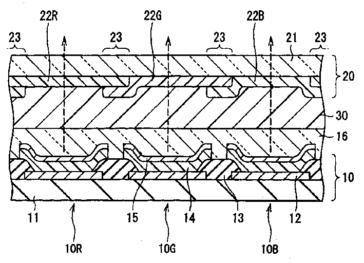
图1示出了根据本发明的第一实施例的显示器的横截面结构。这种显示器用作超薄型的有机EL彩色显示器。在这种显示器中,例如,驱动面板10和密封面板20面对面设置,它们的整个表面通过中间的粘结剂层30互相粘贴在一起。例如,在驱动面板10中,在由绝缘材料如玻璃制成的用于驱动的基底11上,发射红色光线的有机EL装置10R、发射绿色光线的有机EL装置10G和发射蓝色光线的有机EL装置10B按矩阵形式设置成一个整体。FIG. 1 shows a cross-sectional structure of a display according to a first embodiment of the present invention. This display is used as an ultra-thin organic EL color display. In such a display, for example, a driving
有机EL装置10R、10G和10B的每一个具有这样的结构,例如,作为第一电极的阳极12、绝缘层13、有机层14和作为第二电极的阴极15按上述顺序叠加在驱动基底11上。有机EL装置10R、10G和10B由例如氮化硅(SiN)制成的保护层(钝化)16覆盖。保护层16用来防止水份和氧气进入有机EL装置10R、10G和10B而产生腐蚀。Each of the
阳极12,例如,在叠加方向上的厚度(下文简称为厚度)为约200nm,并由诸如铂(Pt)、金(Au)、银(Ag)、铬(Cr)或钨(W)等金属制成,或者由这些金属中任一种的合金制成。The
绝缘层13用来确保阳极12和阴极15之间绝缘,并使在有机EL装置10R、10G和10B的发光区域的形状精确为预定的形状。绝缘层13具有,例如约600nm的厚度。由诸如二氧化硅(SiO2)的绝缘材料制成,并且相应于发光区域具有孔13A。The insulating
在有机EL装置10R、10G和10B中有机层14的结构是可变的。图2放大地示出了有机EL装置10R和10G中有机层14的结构。在每个有机EL装置10R和10G中,有机层14具有如下的结构:分别由有机材料制成的孔注入层14A、孔输送层14B和发光层14C按上述顺序叠加在阳极12上。孔注入层14A和孔输送层14B用来增加至发光层14C的孔注入效率。在相应于绝缘层13的孔13A的区域,靠电流的通过,发光层14C产生光线。The structure of the
在有机EL装置10R中,孔注入层14A具有例如约30nm的厚度,并由4,4′,4″-三(3-甲基苯基苯氨基)三苯胺(MTDAFA)材料制成。孔传输层14B具有约30nm的厚度,并由双[(N-萘基)-N-苯基]联苯胺(2-NPD)材料制成。发光层14C具有例如约40nm的厚度,并由将8-喹啉醇铝络合物(alq)与占体积2%的4-二氰基亚甲基-6-(对-二甲氨基苯乙烯基)-2-甲基-4H-吡喃(DCM)混合形成的材料制成。In the
在有机EL装置10G中,每个孔注入层14A和孔传输层14B都由与有机EL装置10R中类似的材料制成。孔注入层14A的厚度例如约30nm。孔传输层18B的厚度如约20nm。发光层14C的厚度例如约为50nm,并由8-喹啉醇铝络合物(alq)制成。In the
图3是有机EL装置10B中有机层14结构的放大图。在有机EL装置10B中,有机层14具有如下结构:分别由有机材料制成的孔注入层14A、孔传输层14B和发光层14C及电子传输层14D按所述顺序叠加在阳极12上。电子传输层14D用来增加进入发光层14C的注入电子效率。FIG. 3 is an enlarged view of the structure of the
在有机EL装置10B中,孔注入层14A和孔传输层14B由分别与有机EL装置10R和10G中的类似材料制成。孔注入层14A的厚度例如约30nm,孔传输层14B的厚度例如约30nm。发光层14C的厚度约为15nm,并由浴铜灵(BCP)制成。电子传输层14D的厚度例如约30nm,并由alq制成。In the
如图2和图3所示,阴极15具有如下结构:半传输在电子传输层14C中产生的光线的半透明电极15A、传输在发光层14C中产生的光线的透明电极15B按上述顺序叠加在有机层14上。以这种配置,在驱动面板10中,如图1至3中虚线箭头所示,发光层14C中产生的光从阴极15侧射出。As shown in FIGS. 2 and 3 , the
半透明电极15A具有例如约10nm的厚度并由镁(Mg)银(Ag)合金(MgAg合金)制成。半透明电极15A用来使在发光层14C中产生的光在半透明电极15A和阳极12之间反射。即半透明电极15A和阳极12构成共振器的共振部分,来使在发光层14C中产生的光发生共振。优选地按上述方式构成共振器的原因如下。在发光层14C中产生的光造成多重干涉,共振器用作一种窄带滤色器,因此减少发射光谱的半带宽,提高了颜色的纯度。优选地也是为了这个原因:从密封面板20入射的外部光也能被多重干涉减弱,并且通过随后描述的红色滤色器22R、绿色滤色器22G和蓝色滤色器22B(参见图1)的组合,在有机EL装置10R、10G和10B中外部光的反射也可以减小到极低。The
结果优选地,使窄带滤色器的峰值波长和要发射的光谱的峰值波长相互一致。特别是当被阳极12和半透明电极15A反射的反射光的相位移动为φ(弧度),阳极12和半透明电极15A之间的光学距离为L,要从阴极15侧发射的光谱的峰值波长为λ,优选地,光学距离L满足等式1。实际中优选地选择光学距离L使之成为满足等式1的最小负值。在等式1中,L和λ使用相同的单位。作为示例,纳米(nm)用作单位。As a result, it is preferable to make the peak wavelength of the narrowband color filter and the peak wavelength of the spectrum to be emitted coincide with each other. Especially when the phase shift of the reflected light reflected by the
2L/λ+φ/2π=q(q为整数)…等式12L/λ+φ/2π=q (q is an integer)...
透明电极15B用来降低半透明电极15A的电阻率,由相对于发光层14C中产生的光具有足够透射率的导电材料制成。透明电极15B的材料的优选示例是包含钼、锌(Zn)和氧的化合物,原因是即使由该化合物在室温条件下形成的膜片,也可以获得极好的导电性。优选地,透明电极15B的厚度例如约200nm。The
如图1所示,密封面板20设置在驱动面板10的阴极15一侧,具有用粘结剂层30将有机EL装置10R、10G和10B密封在一起的基底21。密封基底21由如玻璃这样的材料制成,对由有机EL装置10R、10G和10B产生的光透明。在密封基底21上,设置有例如红色滤色器22R、绿色滤色器22G、蓝色滤色器22B的滤色器和黑色基体23,由有机EL装置10R、10G和10B产生的光通过其中而射出,并且其吸收被有机EL装置10R、10G和10B和接线电极和设置在装置之间类似物(未示出)反射的外部光,因此提高了对比度。As shown in FIG. 1 , the sealing
红色、绿色和蓝色滤色器22R、22G和22B及黑色基体23可以设置在密封基底的任意一侧,但是优选的设置在驱动面板一侧,原因是红色、绿色和蓝色滤色器22R、22G和22B和黑色基体23没有暴露至表面且可以被粘结剂层30保护。红色、绿色和蓝色滤色器22R、22G和22B分别按相应于有机EL装置10R、10G和10B的顺序设置。The red, green and
图4为从驱动面板10侧观看的平面视图,示出了红色滤色器22R、绿色滤色器22G和蓝色滤色器22B的结构。在图4中,为方便辨别识红色、绿色和蓝色滤色器22R、22G和22B,在红色、绿色和蓝色滤色器22R、22G和22B上分别标记有字母“R”、“G”、“B”。FIG. 4 is a plan view viewed from the
利用印刷技术在分别面向有机EL装置10R、10G和10B的位置形成红色、绿色和蓝色滤色器22R、22G和22B。均为矩形的红色、绿色和蓝色滤色器22R、22G和22B按三角△形设置。每个红色、绿色和蓝色滤色器22R、22G和22B由混合有色素的树脂制成。通过挑选色素,在作为目标颜色的红色、绿色或蓝色中,波长范围内的光传输率可以调高,其它波长的光传输率被调低。Red, green, and
沿着红色、绿色和蓝色滤色器22R、22G和22B的边界设置有黑色基体23。如图1和5所示,黑色基体23具有如下结构:利用印刷技术将红色、绿色和蓝色滤色器22R、22G和22B中至少两个滤色器叠加,并形成在面向有机EL装置10R、10G和10B的边界区域的位置。A
如图1所示,粘结剂层30覆盖了驱动面板10的一侧的整个表面,在这个侧面设置有有机EL装置10R、10G和10B,因此更为有效地防止有机EL装置10R、10G和10B的腐蚀和泄漏。粘结剂层13不必总是设置得覆盖整个驱动面板10的整个表面,可以设置得至少覆盖有机EL装置10R、10G和10B。粘结剂层30由,例如紫外线固化树脂或高温硬化树脂制成。As shown in FIG. 1, the
例如可以按如下方式制造显示器。For example, a display can be manufactured as follows.
图6A和6B至图8A和8B示出了按工艺顺序制造显示器的方法。首先如图6A所示,例如由上述材料制成的红色滤色器22R形成在由上述材料利用印刷技术制成的密封基底21上,另外,用印刷技术形成了绿色滤色器22G。此刻将红色滤色器22R的周边部分与绿色滤色器22G的周边部分重叠,就形成了黑色基体23。至于印刷技术方法,传统使用的凹版工艺可以使用。具体地讲,首先红色滤色器22R或绿色滤色器22G的材料均匀地施加在未示出的滚子上,然后滚子在未示出的平板上滚动将红色滤色器22R或绿色滤色器22G材料转移到平板上,在该平板上形成有红色滤色器22R或绿色滤色器22G的模板。最后,红色滤色器22R或绿色滤色器22G材料转移到密封基底21上。6A and 6B to 8A and 8B illustrate a method of manufacturing a display in process order. First, as shown in FIG. 6A, for example, a
接下来,如图6B所示,用印刷技术将蓝色滤色器22B形成在密封基底上。此刻将蓝色滤色器22B的周边部分和红色、绿色滤色器22R和22G的周边部分互相重叠就形成了图4所示的黑色基体23。用这种方法就制成了密封面板20。Next, as shown in FIG. 6B, a
如图7A所示,例如,在由上述材料制成的驱动基底11之上,用如DC溅射方法形成有由上述材料制成的多个阳极12。接下来在阳极12上,用如CVD(化学汽相淀积)方法以上述厚度形成了绝缘层13。用如石版技术将相应于发光区域的部分有选择地除去,由此形成了孔13A。As shown in FIG. 7A, for example, on a driving
接下来如图7B所示,使用未示出的表面障板,具有上述厚度和由上述材料制成的孔注入层14A、孔传输层14B、发光层14C和电子传输层14D,用例如逸散(evaporation)的方法在绝缘层13的孔13A的相应位置顺序形成。此刻,当改变根据每个有机EL装置10R、10G和10B使用的表面障板时,为每个有机EL装置10R、10G和10B形成了该绝缘层。因为仅在孔13A处高精度的沉积该绝缘层很困难,整个孔13A被覆盖,且该层被沉积而与绝缘层13的周边稍微重叠。用未示出的表面障板在形成有机层14之后,具有上述厚度和由上述材料制成的半透明电极15A,用例如逸散的方法形成。然后,在半透明电极15A上,用与在半透明电极15A中使用的相同的表面障板,用例如DC溅射的方法形成透明电极15B。最后,有机EL装置10R、10G和10B被由例如上述材料制成的保护层16覆盖。按这种方式形成驱动面板10。Next, as shown in FIG. 7B, using an unillustrated surface mask, the
在形成密封面板20和驱动面板10之后,如图8A所示,驱动基底11的形成有有机EL装置10R、10G和10B的一侧涂覆粘结剂层30,粘结剂层30由例如紫外线固化树脂或高温硬化树脂制成。涂覆通过以下步骤进行:从槽喷嘴型分配器注入树脂,用例如滚子涂覆,屏板印刷或类似的方法。After forming the sealing
如图8B所示,驱动面板10和密封面板20被其间的粘结剂层30相互粘贴。优选的是将密封面板20的形成有红色滤色器22R、绿色滤色器22G和蓝色滤色器22B和黑色基体23的一侧面向驱动面板10。优选的是防止气泡或类似物进入粘结剂层30。随后通过适当的移动,例如在固化粘结剂层30之前移动密封面板20,可将密封面板20和驱动面板10对齐。即有机EL装置10R、10G和10B分别与红色、绿色和蓝色滤色器22R、22G和22B对齐。此时尚未固化粘结剂层,密封面板20和驱动面板10相对可移动约几百μm。最后,用紫外线照射粘结剂层30或按预定的温度加热粘结剂层30,于是固化了粘结剂层30,于是将驱动面板10和密封面板20相互粘贴在一起。通过上述方法,完成图1至5所示的显示器。As shown in FIG. 8B , the driving
在用这种方法制造的显示器中,当预定的电压施加到阳极12和阴极15之间时,电流传到发光层14C,孔和电子重新组合,因此在发光层14C侧的界面上产生了光。光在阳极12和半透明电极15A之间多次反射,穿过阳极15、粘结剂层30、红色、绿色和蓝色滤色器22R、22G和22B和密封基底21,并从密封面板20侧穿出。在这个实施例中,密封面板20设置有红色、绿色和蓝色滤色器22R、22G和22B和黑色基体23,于是防止了从密封面板20入射的外部光被有机EL装置10R、10G和10B和置于装置间的接线电极反射,并且外部光从密封面板20射出。这样就提高了对比度。In the display manufactured in this way, when a predetermined voltage is applied between the
在这个实施例中,具有由半透明电极15A和阳极12构成的共振部分的共振器构造在每个有机EL装置10R、10G和10B中。结果经过多次干涉,要发射的光谱的半带宽减小,颜色纯度提高,外部光减少,红色、绿色和蓝色滤色器22R、22G和22B的组合减少外部光的反射。这样对比度可进一步提高。In this embodiment, a resonator having a resonance section constituted by the
根据上述的实施例,在密封基底21上利用印刷技术形成红色、绿色和蓝色滤色器22R、22G和22B,用重叠红色、绿色和蓝色滤色器22R、22G和22B中至少两个滤色器形成黑色基体23。结果只需为每个红色、绿色和蓝色滤色器22R、22G和22B执行一次印刷工艺(总共三次),就形成了红色、绿色和蓝色滤色器22R、22G和22B,同时也形成了黑色基体23。因此就可以低价方便地制造黑色基体23。诚然,与具有多层铬和铬氧化物或黑树脂膜结构的传统薄膜滤色器相比,因为红色、绿色和蓝色中至少两种颜色重叠,黑色基体23具有较低的形状精度和较低的光学密度。然而在没有背光和没有液晶的有机EL显示器中,即使是可以说为伪黑色的黑色基体23也足以防止装置间的接线电极防止外部光的反射,并足以提高对比度。According to the above-mentioned embodiment, the red, green and
因为每个有机EL装置10R、10G和10B具有包括共振部分的共振器,共振部分由半透明电极15A和阳极12构成,通过使由发光层14C产生的光多次干涉及使共振器作为一种窄带宽滤色器,要发射的光谱的半带宽减小,颜色纯度提高。而且从密封面板20入射的外部光通过多次干涉减弱,于是通过红色、绿色和蓝色滤色器22R、22G和22B的组合,可将有机EL装置10R、10G和10B中外部光的反射减少到极小。这样就提高了对比度。[第二实施例]Since each of the
下面将描述根据本发明的第二实施例的显示器。除了红色、绿色和蓝色滤色器22R、22G和22B按条状设置以外,这种显示器与在第一实施例中参考图1至3描述的一样,如图9所示。因此,相同的附图标记表示相同的组件,其细节将不再重复。A display according to a second embodiment of the present invention will be described below. This display is the same as that described with reference to FIGS. 1 to 3 in the first embodiment, as shown in FIG. 9, except that the red, green, and
在这种显示器中,用印刷技术按条状形成红色、绿色和蓝色滤色器22R、22G和22B。黑色基体23设置在不同颜色的相邻条带之间,也在每个颜色的条带中预定的间隔处设置。以这种配置,如图9中点划线所示,由红色、绿色和蓝色滤色器22R、22G和22B形成了像素25。In this display, red, green, and
具体的如图10B的剖视图所示,例如,作为红色的补偿颜色的蓝色滤色器22B重叠在红色滤色器22R上,因此形成了黑色基体23。类似的,虽然在剖视图中未示出,作为绿色的补偿颜色的红色滤色器22R重叠在绿色滤色器22G之上,包含黄色作为蓝色的补偿颜色的绿色滤色器22G重叠在蓝色滤色器22B之上。Specifically, as shown in the cross-sectional view of FIG. 10B , for example, a
具有图10所示的红色滤色器22R、绿色滤色器22G和蓝色滤色器22B的显示器,可以按图11A和11B所示来制造。具体地,首先,如图11A所示,利用印刷技术将红色滤色器22R形成在密封基底21。红色滤色器22R的图案包括:例如,在重叠在相邻绿色滤色器22G之上的拉长凸出部分22R1,来形成黑色基体23。A display having
接下来,如图11B所示,利用印刷技术形成绿色滤色器22G,于是红色滤色器22R的凸出部分22R1和绿色滤色器22G的条带互相重叠,因此形成了黑色基体23。按与红色滤色器22R的类似方法,绿色滤色器22G也包括重叠在相邻蓝色滤色器22B之上的凸出部分22G1,来形成黑色基体23。最后,如图10A所示,利用印刷技术形成蓝色滤色器22B。蓝色滤色器22B也包括重叠在相邻红色滤色器22R之上的凸出部分22B1,来形成黑色基体23。按这种方法,形成了红色、绿色和蓝色滤色器22R、22G和22B,同时也完成了黑色基体23。Next, as shown in FIG. 11B , the
在形成密封面板20之后,如在第一实施例中描述的,形成了驱动面板10,同时粘结剂层30在中间,密封面板20和驱动面板10互相粘贴在一起。After forming the sealing
根据本实施例,即使在红色、绿色和蓝色滤色器22R、22G和22B按条带设置的情况,通过将红色、绿色和蓝色滤色器22R、22G和22B中的两个滤色器重叠在一起,也可以形成黑色基体23。按与第一实施例类似的方式,仅用三次印刷工艺就可以形成红色、绿色和蓝色滤色器22R、22G和22B,同时形成黑色基体23。因此,靠这简单的制造工艺,就可以以低成本形成红色、绿色和蓝色滤色器22R、22G和22B和黑色基体23,对于有机EL显示器红色、绿色和蓝色滤色器22R、22G和22B和黑色基体23是必需的,并且红色、绿色和蓝色滤色器22R、22G和22B和黑色基体23具有足够的性能和特点。According to this embodiment, even in the case where the red, green and
因为每个凸出部分22R1、22G1和22B1为拉长的外形,所以就不能想着利用印刷技术获得高的外形精度。然而,将凸出部分22R1、22G1和22B1用作黑色基体23,用装置之间的接线电极来防止外部光的反射是足够了。凸出部分22R1、22G1和22B1和相邻于凸出部分22R1、22G1和22B1的红色、绿色和蓝色滤色器22R、22G和22B之间不需要严格的位置对齐。即使由于振动而形成了间隙或重叠部分,也不用担心会对黑色基体23的防止外部光反射功能造成负面影响。[第三实施例]Since each of the protruding portions 22R1, 22G1, and 22B1 has an elongated shape, it cannot be expected to obtain high shape accuracy by printing techniques. However, it is sufficient to use the protruding portions 22R1, 22G1, and 22B1 as the
图12示出了根据本发明的第三实施例的显示器。该显示器与第一实施例中所述的相同,不同之处在于相对于密封基底21的驱动面板10的表面设置有抗反射膜24。相同的组件用相同的附图标记表示,其细节不再描述。Fig. 12 shows a display according to a third embodiment of the invention. This display is the same as that described in the first embodiment except that the surface of the
抗反射膜24用来防止在密封基底21内的外部光的表面反射。在密封基底由例如玻璃制成的情况下,其表面反射率为4%。当显示器中外部光的反射被红色、绿色和蓝色滤色器22R、22G和22B、黑色基体23和类似物所抑制,在密封基底21中的表面反射就不能忽视。The
抗反射膜24优选地由,例如薄膜滤色器构成,其中堆积有二氧化硅(SiO2)、二氧化钛(TiO2)或五氧化二铌(Nb2O5)。可选地,可以在密封基底21上粘贴AR(抗反射)膜形成抗反射膜24。The
如上所述,根据本实施例,除了第一实施例中描述的效果,密封基底21设置有抗反射膜24。结果密封基底21的外部光的表面反射减少,对比度可进一步提高。As described above, according to the present embodiment, in addition to the effects described in the first embodiment, the sealing
虽然前述实施例已经描述了本发明,但本发明不被前述实施例所限,可以有各种修改。例如,虽然在前述实施例中已具体描述了有机EL装置10R、10G和10B的配置,不必设置所有的层,例如绝缘层13和透明电极15B。相反地,还可以设置其它层。虽然本发明也可应用到没有设置半透明电极15A的情况,同样如前述实施例所述,更为优选地是设置具有共振部分的共振器,共振部分由半透明电极15A和阳极构成,原因是在有机EL装置10R、10G和10B中的外部光的反射率可被抑制,对比度进一步提高。Although the foregoing embodiments have described the present invention, the present invention is not limited to the foregoing embodiments, and various modifications are possible. For example, although the configurations of the
另外,虽然在前述实施例中,第一电极设为阳极,第二电极设为阴极,但第一电极也可设为阴极而第二电极设为阳极。在这种情况下,光从阳极一侧发出,并且阳极为半透明电极或透明电极。In addition, although in the foregoing embodiments, the first electrode is set as an anode and the second electrode is set as a cathode, the first electrode may be set as a cathode and the second electrode as an anode. In this case, light is emitted from the anode side, and the anode is a semitransparent electrode or a transparent electrode.
而且在前述实施例中,通过改变有机层14的材料,红色、绿色和蓝色光被发射。本发明也可以应用到通过组合颜色改变介质(CCM)或组合滤色器来产生光的显示器中。Also in the foregoing embodiments, by changing the material of the
根据本发明,在显示器和制造显示器的方法中,利用印刷技术形成了红色、绿色和蓝色滤色器,利用印刷技术红色、绿色和蓝色滤色器中至少两个滤色器相互重叠,形成了黑色基体,其面向有机EL装置的边界区域。于是靠简单的制造工艺,具有有机EL显示器所需的必需和足够性能的滤色器和黑色基体可以低成本形成。According to the present invention, in the display and the method of manufacturing the display, red, green and blue color filters are formed by printing technology, at least two of the red, green and blue color filters are overlapped with each other by printing technology, A black matrix is formed, which faces the border region of the organic EL device. Thus, a color filter and a black matrix having necessary and sufficient properties required for an organic EL display can be formed at low cost by a simple manufacturing process.
在根据本发明的一个方面的显示器中,抗反射膜设置在密封基底上。这样,在密封基底中外部光的反射被减少,对比度被进一步提高。In a display according to an aspect of the present invention, the antireflection film is provided on the sealing substrate. In this way, the reflection of external light in the sealing substrate is reduced, and the contrast is further improved.
在根据本发明的一个方面的显示器中,共振器的共振部分由半透明电极和第一电极构成。结果,在发光层产生的光发生多次干涉,使共振部分起一种窄带宽滤色器的作用,因此便要发射的光谱的半带宽减少,并使颜色纯度提高。另外,利用多次干涉可减少来自密封面板的外部光,通过与滤色器结合可将有机EL装置中的外部光的反射减少至极低。这样,可进一步提高对比度。In a display according to an aspect of the present invention, the resonance portion of the resonator is constituted by the semitransparent electrode and the first electrode. As a result, the light generated in the light-emitting layer interferes multiple times, causing the resonant portion to act as a narrow bandwidth filter, thereby reducing the half-bandwidth of the spectrum to be emitted and increasing color purity. In addition, the use of multiple interference can reduce the external light from the sealing panel, and the reflection of external light in the organic EL device can be reduced to an extremely low level by combining with a color filter. In this way, the contrast can be further improved.
显而易见的根据上述说明,本发明可以有很多修改和变化。因此应当明白在所附权利要求限定的范围内,本发明是可以以示例描述以外的方式实施。Obviously many modifications and variations of the present invention are possible in light of the foregoing teachings. It is therefore to be understood that within the scope of the appended claims the invention may be practiced otherwise than as described in the examples.
Claims (13)
Applications Claiming Priority (6)
| Application Number | Priority Date | Filing Date | Title |
|---|---|---|---|
| JP372949/2001 | 2001-12-06 | ||
| JP372949/01 | 2001-12-06 | ||
| JP2001372949 | 2001-12-06 | ||
| JP305463/02 | 2002-10-21 | ||
| JP305463/2002 | 2002-10-21 | ||
| JP2002305463A JP2003234186A (en) | 2001-12-06 | 2002-10-21 | Display device and method of manufacturing the same |
Publications (2)
| Publication Number | Publication Date |
|---|---|
| CN1426269A true CN1426269A (en) | 2003-06-25 |
| CN1276687C CN1276687C (en) | 2006-09-20 |
Family
ID=26624912
Family Applications (1)
| Application Number | Title | Priority Date | Filing Date |
|---|---|---|---|
| CNB021540055A Expired - Lifetime CN1276687C (en) | 2001-12-06 | 2002-12-05 | Display device and its producing method |
Country Status (6)
| Country | Link |
|---|---|
| US (2) | US6969948B2 (en) |
| JP (1) | JP2003234186A (en) |
| KR (1) | KR100900600B1 (en) |
| CN (1) | CN1276687C (en) |
| SG (1) | SG107123A1 (en) |
| TW (1) | TWI223969B (en) |
Cited By (32)
| Publication number | Priority date | Publication date | Assignee | Title |
|---|---|---|---|---|
| CN1328617C (en) * | 2003-08-12 | 2007-07-25 | 精工爱普生株式会社 | Colour filtering sheet and its making method, display device. photoelectric device and electronic apparatus |
| CN100440531C (en) * | 2004-11-11 | 2008-12-03 | Lg电子株式会社 | Organic electroluminescence display device and manufacturing method thereof |
| CN100444425C (en) * | 2005-08-26 | 2008-12-17 | 中华映管股份有限公司 | Stacked organic electroluminescent device and method for manufacturing the same |
| CN100461977C (en) * | 2005-08-15 | 2009-02-11 | 中华映管股份有限公司 | Organic electroluminescent display device |
| CN100484356C (en) * | 2004-03-05 | 2009-04-29 | 出光兴产株式会社 | Organic electroluminescent display device |
| US7601988B2 (en) | 2004-09-24 | 2009-10-13 | Semiconductor Energy Laboratory Co., Ltd. | Light emitting device |
| CN101305643B (en) * | 2005-11-11 | 2010-05-19 | 富士电机控股株式会社 | Organic el light emitting display |
| CN1868240B (en) * | 2003-09-19 | 2010-06-16 | 索尼株式会社 | Display device and manufacturing method thereof, organic light-emitting device and manufacturing method thereof |
| US8087964B2 (en) | 2005-11-29 | 2012-01-03 | Samsung Mobile Display Co., Ltd. | Method of fabricating organic light emitting diode (OLED) |
| CN102577609A (en) * | 2009-09-09 | 2012-07-11 | 松下电器产业株式会社 | Organic electroluminescent display device |
| CN101562193B (en) * | 2008-04-15 | 2012-12-05 | 精工爱普生株式会社 | Organic electroluminescence apparatus |
| CN101738660B (en) * | 2008-11-20 | 2012-12-26 | 索尼株式会社 | Reflector, display device and manufacturing method thereof |
| US8748875B2 (en) | 2009-11-10 | 2014-06-10 | Panasonic Corporation | Organic electro-luminescence display device |
| CN104347670A (en) * | 2013-08-07 | 2015-02-11 | 三星显示有限公司 | Display panel and manufacturing method thereof |
| CN105633116A (en) * | 2014-12-01 | 2016-06-01 | 昆山国显光电有限公司 | OLED (Organic Light-Emitting Diode) device and manufacturing method therefor, and display apparatus |
| US9905809B2 (en) | 2005-01-21 | 2018-02-27 | Semiconductor Energy Laboratory Co., Ltd. | Light emitting device |
| CN107799572A (en) * | 2017-10-20 | 2018-03-13 | 武汉华星光电半导体显示技术有限公司 | A kind of organic light emitting diode display |
| CN107887411A (en) * | 2016-09-30 | 2018-04-06 | 乐金显示有限公司 | Display device and its manufacture method and the head mounted display including the display device |
| CN108288640A (en) * | 2018-01-31 | 2018-07-17 | 武汉华星光电半导体显示技术有限公司 | OLED display and preparation method thereof |
| CN108417602A (en) * | 2012-10-29 | 2018-08-17 | 精工爱普生株式会社 | Manufacturing method of organic EL device, organic EL device, electronic device |
| CN105633115B (en) * | 2014-11-27 | 2018-11-09 | 昆山国显光电有限公司 | OLED device and its manufacturing method, display device |
| CN109244104A (en) * | 2017-07-10 | 2019-01-18 | 东进世美肯株式会社 | The optical filter of organic luminescent device and organic luminescent device including it |
| CN109904190A (en) * | 2017-12-07 | 2019-06-18 | 三星显示有限公司 | Display device |
| CN110164929A (en) * | 2019-05-17 | 2019-08-23 | 昆山国显光电有限公司 | A kind of organic light-emitting display device |
| CN110323354A (en) * | 2019-04-25 | 2019-10-11 | 昆山工研院新型平板显示技术中心有限公司 | Display panel and display device |
| US10490777B2 (en) | 2018-01-31 | 2019-11-26 | Wuhan China Star Optoelectronics Semiconductor Display Technology Co., Ltd. | OLED display and manufacturing method thereof |
| CN110581159A (en) * | 2014-02-14 | 2019-12-17 | 精工爱普生株式会社 | Manufacturing method of organic light-emitting device, organic light-emitting device, and electronic device |
| CN110707132A (en) * | 2019-09-06 | 2020-01-17 | 武汉华星光电半导体显示技术有限公司 | OLED display panel and manufacturing method thereof |
| US10707274B2 (en) | 2017-10-20 | 2020-07-07 | Wuhan China Star Optoelectronics Semiconductor Display Technology Co., Ltd. | Display panel and manufacturing method thereof |
| CN112099122A (en) * | 2020-09-24 | 2020-12-18 | 深圳市奥视微科技有限公司 | Filter film and display device |
| WO2021035550A1 (en) * | 2019-08-27 | 2021-03-04 | 京东方科技集团股份有限公司 | Manufacturing method of color filter layer, and display substrate and manufacturing method thereof |
| CN115602068A (en) * | 2017-09-12 | 2023-01-13 | 康宁公司(Us) | Dead front end for decorating displays including touch panels on glass and related methods |
Families Citing this family (91)
| Publication number | Priority date | Publication date | Assignee | Title |
|---|---|---|---|---|
| US6825488B2 (en) * | 2000-01-26 | 2004-11-30 | Semiconductor Energy Laboratory Co., Ltd. | Semiconductor device and manufacturing method thereof |
| JP3724725B2 (en) | 2001-11-01 | 2005-12-07 | ソニー株式会社 | Manufacturing method of display device |
| JP3705264B2 (en) * | 2001-12-18 | 2005-10-12 | セイコーエプソン株式会社 | Display device and electronic device |
| TW588571B (en) * | 2002-05-24 | 2004-05-21 | Sanyo Electric Co | Electroluminescence display device |
| GB2391686B (en) * | 2002-07-31 | 2006-03-22 | Dainippon Printing Co Ltd | Electroluminescent display and process for producing the same |
| US7081704B2 (en) * | 2002-08-09 | 2006-07-25 | Semiconductor Energy Laboratory Co., Ltd. | Semiconductor device and manufacturing method thereof |
| JP4651922B2 (en) * | 2002-08-09 | 2011-03-16 | 株式会社半導体エネルギー研究所 | EL display device |
| JP4300396B2 (en) * | 2002-09-20 | 2009-07-22 | 富士ゼロックス株式会社 | Display element manufacturing method and display element |
| JP3703028B2 (en) * | 2002-10-04 | 2005-10-05 | ソニー株式会社 | Display element and display device using the same |
| US7710019B2 (en) * | 2002-12-11 | 2010-05-04 | Samsung Electronics Co., Ltd. | Organic light-emitting diode display comprising auxiliary electrodes |
| KR100895313B1 (en) * | 2002-12-11 | 2009-05-07 | 삼성전자주식회사 | Organic light emitting panel |
| US20040140757A1 (en) * | 2003-01-17 | 2004-07-22 | Eastman Kodak Company | Microcavity OLED devices |
| US20040155576A1 (en) * | 2003-01-17 | 2004-08-12 | Eastman Kodak Company | Microcavity OLED device |
| JP2004229062A (en) * | 2003-01-24 | 2004-08-12 | Pioneer Electronic Corp | Three-dimensional image display device and method for manufacturing same |
| JP3915734B2 (en) * | 2003-05-12 | 2007-05-16 | ソニー株式会社 | Vapor deposition mask, display device manufacturing method using the same, and display device |
| JP4359091B2 (en) * | 2003-07-16 | 2009-11-04 | パイオニア株式会社 | Organic electroluminescence display panel |
| US7030553B2 (en) * | 2003-08-19 | 2006-04-18 | Eastman Kodak Company | OLED device having microcavity gamut subpixels and a within gamut subpixel |
| KR100552962B1 (en) * | 2003-08-28 | 2006-02-15 | 삼성에스디아이 주식회사 | Organic electroluminescent display and manufacturing method thereof |
| JP4403399B2 (en) * | 2003-09-19 | 2010-01-27 | ソニー株式会社 | Display device and manufacturing method of display device |
| JP4716699B2 (en) | 2003-09-30 | 2011-07-06 | 三洋電機株式会社 | Organic EL panel |
| JP4497881B2 (en) * | 2003-09-30 | 2010-07-07 | 三洋電機株式会社 | Organic EL device and organic EL panel |
| JP4428979B2 (en) * | 2003-09-30 | 2010-03-10 | 三洋電機株式会社 | Organic EL panel |
| JP4595955B2 (en) * | 2003-10-23 | 2010-12-08 | セイコーエプソン株式会社 | Organic EL device manufacturing method, organic EL device, and electronic apparatus |
| WO2005086539A1 (en) * | 2004-03-05 | 2005-09-15 | Idemitsu Kosan Co., Ltd. | Organic electroluminescence display device |
| JP5430048B2 (en) * | 2004-03-31 | 2014-02-26 | 双葉電子工業株式会社 | Self-luminous display device |
| JP2005302313A (en) * | 2004-04-06 | 2005-10-27 | Idemitsu Kosan Co Ltd | Organic EL display device and full color device |
| US7129634B2 (en) * | 2004-04-07 | 2006-10-31 | Eastman Kodak Company | Color OLED with added color gamut pixels |
| US7180238B2 (en) * | 2004-04-08 | 2007-02-20 | Eastman Kodak Company | Oled microcavity subpixels and color filter elements |
| KR101098343B1 (en) * | 2004-06-03 | 2011-12-26 | 삼성전자주식회사 | Electro-luminescent display device, color filter panel and method for manufacturing there of |
| JP2006032010A (en) * | 2004-07-13 | 2006-02-02 | Hitachi Displays Ltd | Organic EL display device |
| US7316756B2 (en) * | 2004-07-27 | 2008-01-08 | Eastman Kodak Company | Desiccant for top-emitting OLED |
| WO2006013373A2 (en) * | 2004-08-04 | 2006-02-09 | Cambridge Display Technology Limited | Organic electroluminescent device |
| CA2577342A1 (en) * | 2004-08-23 | 2006-03-02 | National Research Council Of Canada | High performance light-emitting devices |
| JP4747626B2 (en) * | 2005-03-25 | 2011-08-17 | セイコーエプソン株式会社 | Light emitting device |
| JP4830328B2 (en) * | 2005-03-25 | 2011-12-07 | セイコーエプソン株式会社 | Light emitting device |
| US20060290276A1 (en) * | 2005-06-22 | 2006-12-28 | Eastman Kodak Company | OLED device having spacers |
| US8729795B2 (en) | 2005-06-30 | 2014-05-20 | Semiconductor Energy Laboratory Co., Ltd. | Light emitting device and electronic device |
| JP4378366B2 (en) * | 2005-08-04 | 2009-12-02 | キヤノン株式会社 | Light emitting element array |
| TWI299239B (en) | 2005-11-10 | 2008-07-21 | Au Optronics Corp | Organic light emitting display |
| JP2007173083A (en) * | 2005-12-22 | 2007-07-05 | Canon Inc | Light emitting device |
| US7336023B2 (en) * | 2006-02-08 | 2008-02-26 | Youh Meng-Jey | Cold cathode field emission devices having selective wavelength radiation |
| KR101244898B1 (en) * | 2006-06-28 | 2013-03-19 | 삼성디스플레이 주식회사 | Organic Thin Film Transistor Substrate And Fabricating Method Thereof |
| JP2008059791A (en) * | 2006-08-29 | 2008-03-13 | Canon Inc | Organic EL element array |
| US7924272B2 (en) * | 2006-11-27 | 2011-04-12 | Microsoft Corporation | Infrared sensor integrated in a touch panel |
| KR100858823B1 (en) * | 2007-05-30 | 2008-09-17 | 삼성에스디아이 주식회사 | Organic light emitting display |
| JP5470689B2 (en) * | 2007-08-30 | 2014-04-16 | ソニー株式会社 | Display device |
| JP4858379B2 (en) * | 2007-09-18 | 2012-01-18 | セイコーエプソン株式会社 | LIGHT EMITTING DEVICE AND ELECTRONIC DEVICE |
| JP5217791B2 (en) * | 2007-10-18 | 2013-06-19 | セイコーエプソン株式会社 | LIGHT EMITTING DEVICE AND ELECTRONIC DEVICE |
| JP2010282992A (en) * | 2009-06-02 | 2010-12-16 | Sony Corp | Solid-state imaging device, manufacturing method thereof, and electronic apparatus |
| KR101065410B1 (en) * | 2009-07-28 | 2011-09-16 | 삼성모바일디스플레이주식회사 | Organic light emitting display |
| US9244204B2 (en) * | 2009-10-27 | 2016-01-26 | Dai Nippon Printing Co., Ltd. | Image source unit and image display unit |
| US9563004B2 (en) | 2009-10-27 | 2017-02-07 | Dai Nippon Printing Co., Ltd. | Image source unit and image display unit |
| JP5423325B2 (en) * | 2009-11-10 | 2014-02-19 | ソニー株式会社 | Light emitting device and manufacturing method thereof |
| KR101307555B1 (en) * | 2009-12-28 | 2013-09-12 | 엘지디스플레이 주식회사 | Manufacturing method of a flat panel display device |
| JP5445364B2 (en) * | 2010-07-09 | 2014-03-19 | セイコーエプソン株式会社 | ORGANIC EL DEVICE, METHOD FOR MANUFACTURING ORGANIC EL DEVICE, AND ELECTRONIC DEVICE |
| FR2962853A1 (en) * | 2010-07-13 | 2012-01-20 | Commissariat Energie Atomique | ORGANIC ELECTROLUMINESCENT DIODE AND SCREEN WITH LOW REFLECTIVITY. |
| JP5605050B2 (en) * | 2010-07-21 | 2014-10-15 | セイコーエプソン株式会社 | Manufacturing method of organic EL device |
| JP5459142B2 (en) * | 2010-08-11 | 2014-04-02 | セイコーエプソン株式会社 | ORGANIC EL DEVICE, METHOD FOR MANUFACTURING ORGANIC EL DEVICE, AND ELECTRONIC DEVICE |
| JP5720887B2 (en) * | 2011-03-30 | 2015-05-20 | ソニー株式会社 | Display device and electronic device |
| JP6216540B2 (en) * | 2012-05-30 | 2017-10-18 | ローム株式会社 | ORGANIC EL LIGHT EMITTING DEVICE, ITS MANUFACTURING METHOD, AND LAMINATED COLOR FILTER |
| JP5573898B2 (en) * | 2012-08-10 | 2014-08-20 | 大日本印刷株式会社 | Color filter for organic electroluminescence display |
| JP6019997B2 (en) | 2012-09-26 | 2016-11-02 | ソニー株式会社 | Display device and electronic device |
| TWI599082B (en) | 2012-10-09 | 2017-09-11 | 財團法人工業技術研究院 | Brightening self-illuminating display |
| KR20230015519A (en) * | 2012-10-30 | 2023-01-31 | 가부시키가이샤 한도오따이 에네루기 켄큐쇼 | Light-emitting panel, display device, and method for manufacturing light-emitting panel |
| TWI518381B (en) | 2013-03-08 | 2016-01-21 | 元太科技工業股份有限公司 | Color filter and display |
| JP6564559B2 (en) * | 2013-05-10 | 2019-08-21 | 株式会社半導体エネルギー研究所 | Display panel and electronic equipment |
| JP6191287B2 (en) | 2013-07-05 | 2017-09-06 | ソニー株式会社 | Display device |
| JP6248522B2 (en) * | 2013-10-03 | 2017-12-20 | 大日本印刷株式会社 | Organic electroluminescence display device |
| JP2015144087A (en) | 2014-01-31 | 2015-08-06 | ソニー株式会社 | Organic electroluminescent device and electronic device |
| CN103943662B (en) * | 2014-04-21 | 2017-03-15 | 上海和辉光电有限公司 | Full-color organic LED structure and preparation method thereof |
| KR102369095B1 (en) * | 2014-10-07 | 2022-03-02 | 엘지디스플레이 주식회사 | Display device |
| JP6520065B2 (en) * | 2014-11-19 | 2019-05-29 | 大日本印刷株式会社 | Organic LED display device with color filter, method of manufacturing the same, and color filter with antireflective layer |
| KR102487880B1 (en) * | 2014-11-25 | 2023-01-11 | 엘지디스플레이 주식회사 | Organic light emitting display device |
| CN105140247B (en) * | 2015-10-10 | 2018-02-16 | 京东方科技集团股份有限公司 | Organic LED array substrate, manufacture method and use its display |
| JP2018081799A (en) | 2016-11-15 | 2018-05-24 | セイコーエプソン株式会社 | Electro-optical device, method of manufacturing electro-optical device, and electronic apparatus |
| JP6930092B2 (en) | 2016-11-17 | 2021-09-01 | セイコーエプソン株式会社 | Electro-optic equipment, manufacturing method of electro-optical equipment, and electronic devices |
| KR102502221B1 (en) * | 2017-08-08 | 2023-02-21 | 삼성디스플레이 주식회사 | Color conversion element and display device comprising the same |
| CN107634149B (en) * | 2017-09-14 | 2025-07-18 | 京东方科技集团股份有限公司 | Display device and method for manufacturing the same |
| JP7130411B2 (en) * | 2018-04-03 | 2022-09-05 | キヤノン株式会社 | Light emitting device, display device and imaging device |
| JP7418949B2 (en) * | 2018-04-03 | 2024-01-22 | キヤノン株式会社 | Display device, imaging device |
| JPWO2019220283A1 (en) | 2018-05-18 | 2021-07-01 | 株式会社半導体エネルギー研究所 | Light emitting elements, light emitting devices, electronic devices and lighting devices |
| US10581011B2 (en) * | 2018-06-01 | 2020-03-03 | Int Tech Co., Ltd. | Light emitting device with different light emitting material overlapping width |
| JPWO2020003056A1 (en) * | 2018-06-29 | 2021-08-02 | 株式会社半導体エネルギー研究所 | Display panel, display device, input / output device, information processing device |
| CN109148718B (en) * | 2018-08-20 | 2020-08-04 | 武汉华星光电半导体显示技术有限公司 | Organic light-emitting display panel and manufacturing method thereof |
| JP7612319B2 (en) * | 2019-07-30 | 2025-01-14 | エルジー ディスプレイ カンパニー リミテッド | Display device |
| KR102806913B1 (en) * | 2020-02-27 | 2025-05-15 | 삼성디스플레이 주식회사 | Display device |
| US20210305324A1 (en) * | 2020-03-30 | 2021-09-30 | Canon Kabushiki Kaisha | Color filter array, electronic device, and method of manufacturing color filter array |
| EP3993055B1 (en) * | 2020-05-15 | 2023-08-16 | BOE Technology Group Co., Ltd. | Display substrate, preparation method therefor, and display apparatus |
| KR20220110409A (en) * | 2021-01-29 | 2022-08-08 | 삼성디스플레이 주식회사 | Display device |
| KR20240108048A (en) * | 2022-12-30 | 2024-07-09 | 엘지디스플레이 주식회사 | Display apparatus |
| WO2024252856A1 (en) * | 2023-06-07 | 2024-12-12 | ソニーセミコンダクタソリューションズ株式会社 | Display device and electronic device |
Family Cites Families (26)
| Publication number | Priority date | Publication date | Assignee | Title |
|---|---|---|---|---|
| JPS63173023A (en) * | 1987-01-13 | 1988-07-16 | Matsushita Electric Ind Co Ltd | Manufacturing method of color filter for liquid crystal display |
| JPH02287303A (en) | 1989-04-28 | 1990-11-27 | Ube Ind Ltd | multilayer color filter |
| JP2680721B2 (en) * | 1990-07-02 | 1997-11-19 | シャープ株式会社 | Thin film EL panel |
| US5239228A (en) * | 1990-07-02 | 1993-08-24 | Sharp Kabushiki Kaisha | Thin-film electroluminescence device for displaying multiple colors with groove for capturing adhesive |
| JP2823725B2 (en) * | 1992-01-18 | 1998-11-11 | シャープ株式会社 | Color thin film EL panel |
| JP2998826B2 (en) * | 1993-12-22 | 2000-01-17 | 凸版印刷株式会社 | Manufacturing method of color filter |
| US5668649A (en) * | 1994-03-07 | 1997-09-16 | Hitachi, Ltd. | Structure of liquid crystal display device for antireflection |
| JPH0895024A (en) * | 1994-09-28 | 1996-04-12 | Canon Inc | Color filter, manufacturing method thereof, and liquid crystal display panel incorporating the same color filter |
| JP2838063B2 (en) * | 1995-09-20 | 1998-12-16 | 出光興産株式会社 | Organic electroluminescence device |
| US5780174A (en) * | 1995-10-27 | 1998-07-14 | Kabushiki Kaisha Toyota Chuo Kenkyusho | Micro-optical resonator type organic electroluminescent device |
| JP3591676B2 (en) | 1996-08-19 | 2004-11-24 | シャープ株式会社 | Liquid crystal display |
| EP0845812B1 (en) * | 1996-11-28 | 2009-10-28 | Casio Computer Co., Ltd. | Display apparatus |
| JP2000029014A (en) | 1998-07-07 | 2000-01-28 | Sharp Corp | Color filter substrate for liquid crystal display device and liquid crystal display device |
| JP2000047007A (en) * | 1998-07-31 | 2000-02-18 | Sony Corp | Anti-reflection film and cathode ray tube |
| JP3558533B2 (en) | 1998-09-16 | 2004-08-25 | シャープ株式会社 | Liquid crystal display |
| TW516244B (en) * | 1999-09-17 | 2003-01-01 | Semiconductor Energy Lab | EL display device and method for manufacturing the same |
| US6641933B1 (en) * | 1999-09-24 | 2003-11-04 | Semiconductor Energy Laboratory Co., Ltd. | Light-emitting EL display device |
| JP2001126862A (en) * | 1999-10-25 | 2001-05-11 | Futaba Corp | Organic electroluminescent device with color filter |
| EP2154737A3 (en) * | 1999-11-22 | 2012-06-20 | Sony Corporation | Display device |
| TW465122B (en) * | 1999-12-15 | 2001-11-21 | Semiconductor Energy Lab | Light-emitting device |
| JP2001181821A (en) | 1999-12-20 | 2001-07-03 | Murata Mfg Co Ltd | Vacuum film deposition system |
| US6646692B2 (en) * | 2000-01-26 | 2003-11-11 | Semiconductor Energy Laboratory Co., Ltd. | Liquid-crystal display device and method of fabricating the same |
| JP2001230072A (en) * | 2000-02-18 | 2001-08-24 | Denso Corp | Organic el display device |
| JP2001267070A (en) * | 2000-03-22 | 2001-09-28 | Sharp Corp | Method for manufacturing color EL display device |
| JP2002221616A (en) * | 2000-11-21 | 2002-08-09 | Seiko Epson Corp | Color filter manufacturing method and manufacturing apparatus, liquid crystal device manufacturing method and manufacturing apparatus, EL device manufacturing method and manufacturing apparatus, inkjet head control apparatus, material discharging method and material discharging apparatus, and electronic equipment |
| JP3613257B2 (en) * | 2001-05-02 | 2005-01-26 | セイコーエプソン株式会社 | Color display substrate, color filter substrate, color light emission substrate, color display substrate manufacturing method, electro-optical device, electronic device |
-
2002
- 2002-10-21 JP JP2002305463A patent/JP2003234186A/en not_active Withdrawn
- 2002-11-19 US US10/299,652 patent/US6969948B2/en not_active Expired - Lifetime
- 2002-11-20 TW TW091133821A patent/TWI223969B/en not_active IP Right Cessation
- 2002-12-02 SG SG200207368A patent/SG107123A1/en unknown
- 2002-12-05 CN CNB021540055A patent/CN1276687C/en not_active Expired - Lifetime
- 2002-12-05 KR KR1020020076882A patent/KR100900600B1/en not_active Expired - Fee Related
-
2004
- 2004-01-20 US US10/760,892 patent/US6971938B2/en not_active Expired - Lifetime
Cited By (51)
| Publication number | Priority date | Publication date | Assignee | Title |
|---|---|---|---|---|
| CN1328617C (en) * | 2003-08-12 | 2007-07-25 | 精工爱普生株式会社 | Colour filtering sheet and its making method, display device. photoelectric device and electronic apparatus |
| CN1868240B (en) * | 2003-09-19 | 2010-06-16 | 索尼株式会社 | Display device and manufacturing method thereof, organic light-emitting device and manufacturing method thereof |
| CN100484356C (en) * | 2004-03-05 | 2009-04-29 | 出光兴产株式会社 | Organic electroluminescent display device |
| US8723196B2 (en) | 2004-09-24 | 2014-05-13 | Semiconductor Energy Laboratory Co., Ltd. | Light emitting device |
| US8450755B2 (en) | 2004-09-24 | 2013-05-28 | Semiconductor Energy Laboratory Co., Ltd. | Light emitting device |
| US7601988B2 (en) | 2004-09-24 | 2009-10-13 | Semiconductor Energy Laboratory Co., Ltd. | Light emitting device |
| CN101027942B (en) * | 2004-09-24 | 2010-06-16 | 株式会社半导体能源研究所 | Light emitting device |
| US7875893B2 (en) | 2004-09-24 | 2011-01-25 | Semiconductor Energy Laboratory Co., Ltd. | Light emitting device |
| US8188491B2 (en) | 2004-09-24 | 2012-05-29 | Semiconductor Energy Laboratory Co., Ltd. | Light emitting device |
| CN100440531C (en) * | 2004-11-11 | 2008-12-03 | Lg电子株式会社 | Organic electroluminescence display device and manufacturing method thereof |
| US10333108B2 (en) | 2005-01-21 | 2019-06-25 | Semiconductor Energy Laboratory Co., Ltd. | Light emitting device |
| US9905809B2 (en) | 2005-01-21 | 2018-02-27 | Semiconductor Energy Laboratory Co., Ltd. | Light emitting device |
| CN100461977C (en) * | 2005-08-15 | 2009-02-11 | 中华映管股份有限公司 | Organic electroluminescent display device |
| CN100444425C (en) * | 2005-08-26 | 2008-12-17 | 中华映管股份有限公司 | Stacked organic electroluminescent device and method for manufacturing the same |
| CN101305643B (en) * | 2005-11-11 | 2010-05-19 | 富士电机控股株式会社 | Organic el light emitting display |
| US8087964B2 (en) | 2005-11-29 | 2012-01-03 | Samsung Mobile Display Co., Ltd. | Method of fabricating organic light emitting diode (OLED) |
| US8400055B2 (en) | 2008-04-15 | 2013-03-19 | Seiko Epson Corporation | Organic electroluminescence apparatus with metal auxiliary wiring |
| CN101562193B (en) * | 2008-04-15 | 2012-12-05 | 精工爱普生株式会社 | Organic electroluminescence apparatus |
| CN101738660B (en) * | 2008-11-20 | 2012-12-26 | 索尼株式会社 | Reflector, display device and manufacturing method thereof |
| CN102577609A (en) * | 2009-09-09 | 2012-07-11 | 松下电器产业株式会社 | Organic electroluminescent display device |
| US8748875B2 (en) | 2009-11-10 | 2014-06-10 | Panasonic Corporation | Organic electro-luminescence display device |
| CN102577610B (en) * | 2009-11-10 | 2015-04-08 | 松下电器产业株式会社 | Organic electroluminescence display apparatus |
| CN108417602B (en) * | 2012-10-29 | 2022-03-29 | 精工爱普生株式会社 | Method for manufacturing organic EL device, and electronic apparatus |
| CN108417602A (en) * | 2012-10-29 | 2018-08-17 | 精工爱普生株式会社 | Manufacturing method of organic EL device, organic EL device, electronic device |
| CN104347670A (en) * | 2013-08-07 | 2015-02-11 | 三星显示有限公司 | Display panel and manufacturing method thereof |
| CN104347670B (en) * | 2013-08-07 | 2021-03-09 | 三星显示有限公司 | Display panel and method for manufacturing the same |
| CN110581159B (en) * | 2014-02-14 | 2023-08-25 | 精工爱普生株式会社 | Manufacturing method of organic light-emitting device, organic light-emitting device, and electronic device |
| CN110581159A (en) * | 2014-02-14 | 2019-12-17 | 精工爱普生株式会社 | Manufacturing method of organic light-emitting device, organic light-emitting device, and electronic device |
| CN105633115B (en) * | 2014-11-27 | 2018-11-09 | 昆山国显光电有限公司 | OLED device and its manufacturing method, display device |
| CN105633116B (en) * | 2014-12-01 | 2018-11-13 | 昆山国显光电有限公司 | OLED device and its manufacturing method, display device |
| CN105633116A (en) * | 2014-12-01 | 2016-06-01 | 昆山国显光电有限公司 | OLED (Organic Light-Emitting Diode) device and manufacturing method therefor, and display apparatus |
| CN107887411B (en) * | 2016-09-30 | 2021-12-10 | 乐金显示有限公司 | Display device, method of manufacturing the same, and head-mounted display including the same |
| CN107887411A (en) * | 2016-09-30 | 2018-04-06 | 乐金显示有限公司 | Display device and its manufacture method and the head mounted display including the display device |
| CN109244104A (en) * | 2017-07-10 | 2019-01-18 | 东进世美肯株式会社 | The optical filter of organic luminescent device and organic luminescent device including it |
| CN109244104B (en) * | 2017-07-10 | 2024-09-17 | 东进世美肯株式会社 | Optical filter of organic light emitting device and organic light emitting device including the same |
| CN115602068A (en) * | 2017-09-12 | 2023-01-13 | 康宁公司(Us) | Dead front end for decorating displays including touch panels on glass and related methods |
| CN107799572A (en) * | 2017-10-20 | 2018-03-13 | 武汉华星光电半导体显示技术有限公司 | A kind of organic light emitting diode display |
| US10707274B2 (en) | 2017-10-20 | 2020-07-07 | Wuhan China Star Optoelectronics Semiconductor Display Technology Co., Ltd. | Display panel and manufacturing method thereof |
| WO2019075814A1 (en) * | 2017-10-20 | 2019-04-25 | 武汉华星光电半导体显示技术有限公司 | Organic light-emitting diode display |
| CN109904190A (en) * | 2017-12-07 | 2019-06-18 | 三星显示有限公司 | Display device |
| CN108288640A (en) * | 2018-01-31 | 2018-07-17 | 武汉华星光电半导体显示技术有限公司 | OLED display and preparation method thereof |
| US10490777B2 (en) | 2018-01-31 | 2019-11-26 | Wuhan China Star Optoelectronics Semiconductor Display Technology Co., Ltd. | OLED display and manufacturing method thereof |
| WO2019148594A1 (en) * | 2018-01-31 | 2019-08-08 | 武汉华星光电半导体显示技术有限公司 | Oled display and manufacturing method therefor |
| CN110323354B (en) * | 2019-04-25 | 2021-12-14 | 昆山工研院新型平板显示技术中心有限公司 | Display panel and display device |
| CN110323354A (en) * | 2019-04-25 | 2019-10-11 | 昆山工研院新型平板显示技术中心有限公司 | Display panel and display device |
| CN110164929B (en) * | 2019-05-17 | 2021-06-11 | 昆山国显光电有限公司 | Organic light emitting display device |
| CN110164929A (en) * | 2019-05-17 | 2019-08-23 | 昆山国显光电有限公司 | A kind of organic light-emitting display device |
| WO2021035550A1 (en) * | 2019-08-27 | 2021-03-04 | 京东方科技集团股份有限公司 | Manufacturing method of color filter layer, and display substrate and manufacturing method thereof |
| US11587988B2 (en) | 2019-08-27 | 2023-02-21 | Boe Technology Group Co., Ltd. | Preparation method of color film layer, display substrate and preparation method thereof |
| CN110707132A (en) * | 2019-09-06 | 2020-01-17 | 武汉华星光电半导体显示技术有限公司 | OLED display panel and manufacturing method thereof |
| CN112099122A (en) * | 2020-09-24 | 2020-12-18 | 深圳市奥视微科技有限公司 | Filter film and display device |
Also Published As
| Publication number | Publication date |
|---|---|
| US6969948B2 (en) | 2005-11-29 |
| CN1276687C (en) | 2006-09-20 |
| KR20030047761A (en) | 2003-06-18 |
| KR100900600B1 (en) | 2009-06-02 |
| US20030107314A1 (en) | 2003-06-12 |
| US6971938B2 (en) | 2005-12-06 |
| TW200301066A (en) | 2003-06-16 |
| US20040147200A1 (en) | 2004-07-29 |
| TWI223969B (en) | 2004-11-11 |
| SG107123A1 (en) | 2004-11-29 |
| JP2003234186A (en) | 2003-08-22 |
Similar Documents
| Publication | Publication Date | Title |
|---|---|---|
| CN1276687C (en) | Display device and its producing method | |
| CN100350624C (en) | Display device | |
| JP5708482B2 (en) | Organic electroluminescent device and method of manufacturing organic electroluminescent device | |
| KR101990312B1 (en) | Organic Light Emitting Diode Display Device and Method for Manufacturing The Same | |
| KR101386766B1 (en) | Display unit and manufacturing method thereof | |
| JP5963458B2 (en) | LIGHT EMITTING DEVICE, IMAGE FORMING DEVICE, AND IMAGING DEVICE | |
| CN1607876A (en) | Organic light emitting device, manufacturing method thereof, and display unit | |
| CN1575063A (en) | Laminated structure, manufacturing method thereof, display element, and display unit | |
| CN1722925A (en) | Organic electroluminescence display device | |
| KR20110016402A (en) | Light emitting element | |
| US8183564B2 (en) | Multicolor display apparatus | |
| TW200822414A (en) | Organic EL display | |
| US20130193418A1 (en) | Light-emitting apparatus, image-forming apparatus, display apparatus, and image pickup apparatus | |
| US20060273712A1 (en) | Organic electroluminescence display apparatus | |
| JP2007115419A (en) | Organic light emitting device | |
| JP4832292B2 (en) | Organic electroluminescence display device | |
| JP4736284B2 (en) | Display device and manufacturing method thereof | |
| CN1461180A (en) | Electroluminescent display device | |
| CN1698218A (en) | Light emitting device, manufacturing method thereof, and display unit | |
| JP2011054424A (en) | Top-emission type organic el display and method of manufacturing the same, and color filter used for it | |
| JP2003051380A (en) | Linear light source using organic electroluminescent device and method of manufacturing the same | |
| CN1780511A (en) | EL device and electronic equipment | |
| JP2008130363A (en) | ORGANIC EL ELEMENT AND ITS MANUFACTURING METHOD, ORGANIC EL DISPLAY AND ITS MANUFACTURING METHOD | |
| JP2008103359A (en) | Organic electroluminescence display | |
| JP2005293983A (en) | Spontaneous emission display device |
Legal Events
| Date | Code | Title | Description |
|---|---|---|---|
| C06 | Publication | ||
| PB01 | Publication | ||
| C10 | Entry into substantive examination | ||
| SE01 | Entry into force of request for substantive examination | ||
| C14 | Grant of patent or utility model | ||
| GR01 | Patent grant | ||
| CX01 | Expiry of patent term | ||
| CX01 | Expiry of patent term |
Granted publication date: 20060920 |