CN1204146A - Semiconductor device and its manufacturing method - Google Patents
Semiconductor device and its manufacturing method Download PDFInfo
- Publication number
- CN1204146A CN1204146A CN98105764A CN98105764A CN1204146A CN 1204146 A CN1204146 A CN 1204146A CN 98105764 A CN98105764 A CN 98105764A CN 98105764 A CN98105764 A CN 98105764A CN 1204146 A CN1204146 A CN 1204146A
- Authority
- CN
- China
- Prior art keywords
- film
- oxide film
- field shield
- gate electrode
- oxide
- Prior art date
- Legal status (The legal status is an assumption and is not a legal conclusion. Google has not performed a legal analysis and makes no representation as to the accuracy of the status listed.)
- Granted
Links
Images


Classifications
-
- H—ELECTRICITY
- H01—ELECTRIC ELEMENTS
- H01L—SEMICONDUCTOR DEVICES NOT COVERED BY CLASS H10
- H01L21/00—Processes or apparatus adapted for the manufacture or treatment of semiconductor or solid state devices or of parts thereof
- H01L21/70—Manufacture or treatment of devices consisting of a plurality of solid state components formed in or on a common substrate or of parts thereof; Manufacture of integrated circuit devices or of parts thereof
- H01L21/71—Manufacture of specific parts of devices defined in group H01L21/70
- H01L21/76—Making of isolation regions between components
- H01L21/765—Making of isolation regions between components by field effect
-
- H—ELECTRICITY
- H01—ELECTRIC ELEMENTS
- H01L—SEMICONDUCTOR DEVICES NOT COVERED BY CLASS H10
- H01L21/00—Processes or apparatus adapted for the manufacture or treatment of semiconductor or solid state devices or of parts thereof
- H01L21/70—Manufacture or treatment of devices consisting of a plurality of solid state components formed in or on a common substrate or of parts thereof; Manufacture of integrated circuit devices or of parts thereof
- H01L21/71—Manufacture of specific parts of devices defined in group H01L21/70
- H01L21/76—Making of isolation regions between components
Landscapes
- Engineering & Computer Science (AREA)
- Physics & Mathematics (AREA)
- Condensed Matter Physics & Semiconductors (AREA)
- General Physics & Mathematics (AREA)
- Manufacturing & Machinery (AREA)
- Computer Hardware Design (AREA)
- Microelectronics & Electronic Packaging (AREA)
- Power Engineering (AREA)
- Element Separation (AREA)
- Thin Film Transistor (AREA)
- Insulated Gate Type Field-Effect Transistor (AREA)
Abstract
以提供解决了由FS绝缘层引起的器件的工作特性和可靠性降低的半导体器件作为第1目的,以提供防止了起因于制造过程而发生的栅氧化膜的破损的半导体器件作为第2目的,以提供防止了起因于FS电极的材料质量而发生的与栅电极的短路的半导体器件作为第3目的。通过在FS电极5的上表面上形成FS上部氮化膜15,在制造工序中,即使在局部几乎除去FS上部氧化膜41的情况下,也可防止FS电极5的上表面露出。

The first object is to provide a semiconductor device that solves the degradation of the operating characteristics and reliability of the device caused by the FS insulating layer, and the second object is to provide a semiconductor device that prevents damage to the gate oxide film caused by the manufacturing process, A third object is to provide a semiconductor device in which a short circuit with a gate electrode due to the material quality of the FS electrode is prevented. By forming the FS upper nitride film 15 on the upper surface of the FS electrode 5, even when the FS upper oxide film 41 is almost partially removed in the manufacturing process, the upper surface of the FS electrode 5 can be prevented from being exposed.
Description
本发明涉及半导体器件及其制造方法,特别是涉及具有场分离结构的半导体器件及其制造方法。The present invention relates to a semiconductor device and a manufacturing method thereof, in particular to a semiconductor device with a field separation structure and a manufacturing method thereof.
图82是表示作为本发明的背景的具有场分离结构的现有的半导体器件M90的剖面结构的剖面斜视图。该半导体器件是作为SOI型的半导体器件来构成的,该SOI型的半导体器件使用了在绝缘性衬底上备有形成为膜状的半导体层、即SOI(在绝缘体上的半导体)层的SOI衬底作为在内部制成晶体管元件等的半导体衬底。FIG. 82 is a cross-sectional perspective view showing a cross-sectional structure of a conventional semiconductor device M90 having a field separation structure as the background of the present invention. This semiconductor device is configured as an SOI type semiconductor device using an SOI substrate having a film-like semiconductor layer, that is, an SOI (semiconductor on insulator) layer formed on an insulating substrate. The bottom serves as a semiconductor substrate in which transistor elements and the like are made.
如图82所示,在半导体器件M90中,在用支撑衬底1和埋入氧化膜2构成的绝缘性衬底上形成硅半导体层作为SOI层3。该SOI层3包含多个NMOS晶体管的形成区(以下称为NMOS区)和PMOS晶体管的形成区(以下称为PMOS区)。然后在SOI层3的各元件区的边界处形成了用于将这些元件区互相电分离开的平板状的场屏蔽电极(以下简称为FS电极)5。As shown in FIG. 82 , in a semiconductor device M90 , a silicon semiconductor layer is formed as an
在SOI层3上隔开预定的间隔平行地配置FS电极5,以便在各元件区中界定有源区。然后,利用场屏蔽绝缘层4(以下简称为FS绝缘层)来覆盖FS电极5,配置栅电极6,使其从有源区上跨过平行的2个FS绝缘层4的上部。再有,在栅电极6和有源区之间形成栅氧化膜10。用氧化物来构成FS绝缘层,利用该FS绝缘层4在FS电极5和栅电极6之间进行电绝缘。
通过图中未示出的绝缘层中设置的接触孔7将漏电极和源电极(图中未示出)、即主电极连接到SOI层3内的源·漏层(图中未示出),通过接触孔8将栅布线(图中未示出)连接到栅电极6上。The drain electrode and the source electrode (not shown in the figure), that is, the main electrode are connected to the source/drain layer (not shown in the figure) in the
此外,通过接触孔9连接体接触(body contact)电极(图中未示出)。再有,在图82中,示出了与体接触电极(图中未示出)连接的接触孔9贯通FS电极5连接到SOI层3的结构,但也可在FS电极5的外侧设置接触孔9。In addition, a body contact electrode (not shown in the figure) is connected through the contact hole 9 . Furthermore, in FIG. 82 , the structure in which the contact hole 9 connected to the body contact electrode (not shown in the figure) penetrates the
在半导体器件M90中,通过对FS电极5施加反偏置电压,分离区的SOI层3呈截止状态,结果可实现元件区之间的电分离。作为用于实现各元件区之间的分离的其他的众所周知的结构,有通过有选择地使SOI层3氧化来实现分离的LOCOS结构,或通过有选择地刻蚀SOI层3将各元件区互相分离开的台面(mesa)分离结构。In the semiconductor device M90, by applying a reverse bias voltage to the
但是,为了形成这些LOCOS结构或台面(mesa)分离结构,必须对SOI层3进行局部的氧化处理或局部的刻蚀处理,因此在SOI层3的局部产生应力集中的现象。其结果是存在导致漏泄电流的产生等的器件的可靠性方面的问题。与此相反,在场分离结构的形成中,不需要局部的氧化、刻蚀等工序。因此,具有下述优点:可避免应力的集中,抑制漏泄电流,可得到较高的可靠性。However, in order to form these LOCOS structures or mesa separation structures, the
再有,根据先有技术的调查结果得到了以下所示的文献,现列举这些文献的概要。在特开平8-162523号公报中示出了在屏蔽栅电极的上部具有由氮化硅膜构成的顶盖绝缘膜、对屏蔽栅电极的侧面进行热氧化来代替侧壁绝缘膜的结构。In addition, the documents shown below were obtained as a result of prior art investigation, and the outlines of these documents are listed below. Japanese Unexamined Patent Publication No. 8-162523 discloses a structure in which a cap insulating film made of a silicon nitride film is provided on top of a shield gate electrode, and the side surfaces of the shield gate electrode are thermally oxidized instead of the sidewall insulating film.
在特开平7-201967号公报中示出了对多晶硅膜的侧面进行热氧化减小由多晶硅膜构成的场屏蔽电极的宽度的结构。Japanese Unexamined Patent Publication No. 7-201967 shows a structure in which the side surface of a polysilicon film is thermally oxidized to reduce the width of a field shield electrode made of a polysilicon film.
在特开平8-31928号公报中示出了依次形成屏蔽栅氧化膜、氮化硅膜、多晶硅膜的结构。JP-A-8-31928 discloses a structure in which a gate oxide film, a silicon nitride film, and a polysilicon film are sequentially formed.
在特开平6-302779号公报中示出了在ONO膜上形成了屏蔽板电极的结构。Japanese Unexamined Patent Publication No. 6-302779 shows a structure in which a shield plate electrode is formed on an ONO film.
在特开平7-283300号公报和特开平9-27600号公报中示出了用氮化硅膜覆盖屏蔽电极的上部和侧面的结构。JP-A-7-283300 and JP-A-9-27600 show structures in which the upper portion and side surfaces of a shield electrode are covered with a silicon nitride film.
但是,在现有的场分离结构中,起因于该结构和制造方法的可靠性方面的各种问题仍然没有得到解决。However, in the existing field separation structure, various problems arising from the reliability of the structure and the manufacturing method have not yet been solved.
以下,一边使用图83~图101按顺序说明现有的场分离结构的形成工序,一边谈及这些问题。Hereinafter, these problems will be discussed while sequentially describing the steps of forming a conventional field separation structure using FIGS. 83 to 101 .
首先如图83所示,首先在SOI衬底的SOI层3的表面上按顺序形成氧化膜OF1、掺了杂质(例如磷)的多晶硅层PS1、氧化膜OF2。其中,各层的厚度是这样的:SOI层3约为1000埃,氧化膜OF1约为200埃,多晶硅层PS1约为500埃,氧化膜OF2约为1000埃。First, as shown in FIG. 83, an oxide film OF1, a polysilicon layer PS1 doped with impurities (for example, phosphorus), and an oxide film OF2 are sequentially formed on the surface of the
其次,在图84中示出的工序中,在氧化膜OF2上形成经图形刻蚀的抗蚀剂掩模R1。Next, in the process shown in FIG. 84, a patterned resist mask R1 is formed on the oxide film OF2.
其次,在图85中示出的工序中,以抗蚀剂掩模R1作为掩模,利用各向异性刻蚀(干法刻蚀)有选择地除去氧化膜OF2和多晶硅层PS1,形成FS上部氧化膜(第1氧化膜)41、FS电极5。Next, in the process shown in FIG. 85, the oxide film OF2 and the polysilicon layer PS1 are selectively removed by anisotropic etching (dry etching) using the resist mask R1 as a mask to form the upper part of the FS. Oxide film (first oxide film) 41 ,
其次,在图86中示出的工序中,形成氧化膜OF3,以便覆盖氧化膜OF1、FS上部氧化膜41、FS电极5。再有,氧化膜OF3的厚度是1500~2000埃。Next, in the process shown in FIG. 86 , an oxide film OF3 is formed so as to cover the oxide film OF1 , the FS
然后,在图87中示出的工序中,利用各向异性刻蚀(干法刻蚀)除去氧化膜OF3,在FS上部氧化膜41和FS电极5的侧面形成侧壁氧化膜(第2氧化膜)42。Then, in the process shown in FIG. 87, the oxide film OF3 is removed by anisotropic etching (dry etching), and a side wall oxide film (second oxide film) is formed on the side surfaces of the FS
其后,在图88中示出的工序中除去氧化膜OF1。氧化膜OF1可以是用于不使源·漏区暴露于干法刻蚀的等离子体中的保护膜,利用湿法刻蚀将其除去。利用该工序,只在FS电极5和侧壁氧化膜42的下部留下氧化膜OF1,成为FS栅氧化膜43。再有,用FS上部氧化膜41、侧壁氧化膜42、FS栅氧化膜43构成FS绝缘层4。此时,与氧化膜OF1一起,同时也刻蚀FS上部氧化膜41、侧壁氧化膜42,其厚度减少。如果FS上部氧化膜41的厚度变薄,则FS电极5和栅电极6之间的寄生电容增大,导致器件的工作速度下降,同时也容易发生这些电极间的短路故障。Thereafter, the oxide film OF1 is removed in the process shown in FIG. 88 . The oxide film OF1 may be a protective film for preventing the source/drain regions from being exposed to plasma of dry etching, and may be removed by wet etching. In this step, only the oxide film OF1 is left on the lower part of the
其次,在图89中示出的工序中,在SOI层3的表面上利用热氧化法形成作为栅氧化膜10的氧化膜OF4。在形成氧化膜OF4时,氧化剂、即氧通过FS上部氧化膜41、侧壁氧化膜42、FS栅氧化膜43,对FS电极5进行氧化。FS电极5是容易被氧化的掺杂多晶硅层,由于氧化其实际厚度就减少了。Next, in the process shown in FIG. 89 , an oxide film OF4 as
如果FS电极5的厚度减少,则存在下述的可能性:其电阻增加,在器件工作时不能得到充分的场分离效果,不能得到预期的性能。If the thickness of the
此外,由于到达FS电极5的下部的氧将FS电极5的端部氧化,而且也将侧壁氧化膜42的下部的SOI层3氧化,故FS栅氧化膜43的端部的厚度增加,FS电极5的端部成为向上方弯曲的形状。这是由于越靠近端部被氧化的比例越多,越接近中央部分被氧化的比例越少之故引起的。这样一来,如果FS电极5的端部弯曲,则与栅电极6的距离在局部变窄,存在导致与栅电极之间的寄生电容增大或绝缘破坏的可能性。In addition, since the oxygen reaching the lower portion of the
其次,在图90中所示的工序中,在氧化膜OF4和FS绝缘层4的上部利用CVD法形成厚度为1000~1500埃的、作为栅电极6的多晶硅层PS2。Next, in the process shown in FIG. 90, a polysilicon layer PS2 as the
其次,在图91中所示的工序中,利用各向异性刻蚀(干法刻蚀)有选择地除去多晶硅层PS2,形成栅电极6。然后,以栅电极6为掩模有选择地除去氧化膜OF4,形成栅氧化膜10。Next, in the process shown in FIG. 91, the polysilicon layer PS2 is selectively removed by anisotropic etching (dry etching), and the
此时,由于过刻蚀也部分地除去FS上部氧化膜41,FS上部氧化膜41的厚度部分地变薄。在该状态下,在栅电极6的侧面及在源·漏层内形成用于形成低掺杂漏层(以下称为LDD层)的侧壁氧化膜61。侧壁氧化膜61是这样来形成的:在形成氧化膜使其覆盖栅电极之后,通过利用各向异性刻蚀(干法刻蚀)进行除去,在栅电极6的侧面以自对准的方式来形成。此时,由于过刻蚀,进一步除去FS上部氧化膜41。At this time, the FS
其次,在不打算形成硅化物层的部分上全面地形成硅化物保护膜11。硅化物保护膜11是在源·漏层的表面上形成硅化物层会产生器件工作方面的不良情况的半导体元件的源·漏层的表面上设置的一种膜。Next, the silicide
该形成方法是在衬底的整个面上形成了氧化膜之后,利用各向异性刻蚀(干法刻蚀)有选择地进行除去该氧化膜,使硅化物保护膜11覆盖给定的源·漏层的表面,但此时如图92所示,在FS绝缘层4的侧面(侧壁氧化膜42和FS栅氧化膜43的侧面)也以自对准的方式形成该硅化物保护膜11。在形成该硅化物保护膜11时,由于过刻蚀进一步除去FS上部氧化膜41,故FS上部氧化膜41部分地变得极薄。In this formation method, after an oxide film is formed on the entire surface of the substrate, the oxide film is selectively removed by anisotropic etching (dry etching), so that the silicide
此时,由于在栅氧化工序中FS电极5的端部成为弯曲的形状,故如图92所示,有些情况下部分地露出FS电极5。At this time, since the end of the
在该状态下,在栅电极6的上部表面和图中未示出的源·漏层的表面上以自对准的方式形成硅化物膜12。再有,硅化物膜12可以是硅化钴(CoSi2)、硅化钛(TiSi2)或硅化镍(NiSi2)、硅化钨(WSi2)等中的任何一种。由于在多晶硅层、硅层的表面上形成硅化物膜12,故如图93所示,也在FS电极5的露出面上形成硅化物膜12。In this state, the
在FS电极5的露出面上被形成的硅化物膜12处于容易剥离的状态,这是因为FS电极5的露出面的面积较小或在没有完全除去FS上部氧化膜41的状态下形成的。而且,如果剥离下来的硅化物膜12成为导电性的粉尘并残留在半导体器件上的话,会对半导体器件的工作特性造成不良影响,使器件的制造成品率下降。此外,如果伴随硅化物膜12的剥离而部分地丧失FS电极5,则会导致FS电极5呈断线状态,使器件的制造成品率下降。The
此外,在以上已说明的半导体器件的制造工序中,在图87中示出的工序中示出了利用各向异性刻蚀(干法刻蚀)只除去氧化膜OF3来形成侧壁氧化膜42、利用湿法刻蚀除去氧化膜OF1的例子(图88)。但是,可以用干法刻蚀同时除去氧化膜OF3和OF1,在这种情况下产生以下说明的问题。In addition, in the manufacturing process of the semiconductor device described above, in the process shown in FIG. 87 , only the oxide film OF3 is removed by anisotropic etching (dry etching) to form the side
即,在接着图86的工序中,利用各向异性刻蚀(干法刻蚀)除去氧化膜OF3和OF1,形成侧壁氧化膜42,同时只在侧壁氧化膜42的下部留下氧化膜OF1,成为FS栅氧化膜43。此时,如图94所示,存在由于过刻蚀而除去SOI层3的表面的可能性。That is, in the process following FIG. 86 , the oxide films OF3 and OF1 are removed by anisotropic etching (dry etching) to form the side
特别是在侧壁氧化膜42的端部,该部分与其他部分相比被除去的量较多,变成SOI层部分地被挖去的状态。一般认为其原因之一是刻蚀剂的密度的局部的偏离。因此,如图94所示,在侧壁氧化膜42的端部附近的SOI层3的表面上形成凹部DP。In particular, at the edge of the side
在形成侧壁氧化膜42的工序之后,象使用图89所说明的那样,在SOI层3的表面上形成栅氧化膜OF3,但在形成栅氧化膜OF3之前,必须用湿法刻蚀除去在SOI层3的表面上形成的自然氧化膜。此时,与自然氧化膜一起也除去一部分FS上部氧化膜41和侧壁氧化膜42。在图95中示出该状态。After the step of forming the
在图95中,用虚线示出了除去自然氧化膜之前的FS绝缘膜4的位置。如图95所示,由于FS绝缘膜4的退缩,在侧壁氧化膜42的周围形成边缘部EP。In FIG. 95, the position of the
在图96中示出了在该状态下形成作为栅氧化膜的氧化膜OF4的结果。在图96中,以反映边缘部EP的形状的方式形成氧化膜OF4。即,边缘部EP呈遗留在侧壁氧化膜42的周围的状态。在该状态下,如图97所示,如果形成作为栅电极6的多晶硅层PS2,则由于在器件工作时电场集中于边缘部EP,电场强度变高,栅氧化膜破坏的可能性变高,这样就存在栅氧化膜的可靠性降低、进而具有场分离结构的MOS晶体管的可靠性降低的问题。The result of forming the oxide film OF4 as the gate oxide film in this state is shown in FIG. 96 . In FIG. 96, the oxide film OF4 is formed to reflect the shape of the edge portion EP. That is, the edge portion EP remains around the
再有,与图91~图93对应的图是图98~图100,在这些图中示出了在栅氧化工序中同样发生因FS电极5的端部弯曲而引起的问题的情况。98 to 100 correspond to FIGS. 91 to 93 , and these figures show that a problem caused by bending of the end of the
此外,在以上已说明的问题之外,还存在起因于FS电极的材料性质,在FS电极和晶体管的栅电极重合的地方产生电极间短路的问题。Furthermore, in addition to the problems described above, there is also a problem that an inter-electrode short circuit occurs at a place where the FS electrode and the gate electrode of the transistor overlap due to the material properties of the FS electrode.
FS电极5由掺了磷(P)的N型多晶硅来构成,但这样的多晶硅的晶粒直径较大(包含0.2~1微米的晶粒),此外在氧化工序中沿晶粒边界促进了氧化,存在容易出现凹凸形状的现象。The
即,如图89所示,在SOI层的表面上用热氧化法形成作为栅氧化膜10的氧化膜OF4,但此时氧化剂、即氧通过FS上部氧化膜41、侧壁氧化膜42、FS栅氧化膜43,对FS电极5进行氧化。因此,FS电极5的厚度减少、产生弯曲,这种情况以上已说明过,但同时由于以上已说明的原因,FS电极5的表面呈凹凸状态。That is, as shown in FIG. 89, the oxide film OF4 as the
在图101中示意性地示出了该状态。图101是表示FS绝缘膜4、FS电极5、栅电极6的配置状态的斜视图,为了容易看清其结构而给成透视图。This state is schematically shown in FIG. 101 . Fig. 101 is a perspective view showing the arrangement state of the
由于FS电极5的表面呈凹凸状态,如图101所示,在FS电极5的边缘部存在大小凸起部。因而,在器件工作时电场集中于该凸起部,在与FS电极5的边缘部相对的栅电极6之间绝缘被破坏,产生电极间的短路。Since the surface of the
本发明就是为了解决上述的问题而完成的,其第1个目的是提供一种在具有场分离结构的半导体器件中消除了起因于FS绝缘层的器件的工作特性和可靠性降低的半导体器件,其第2个目的是提供一种防止了起因于制造过程而产生的栅氧化膜的破损的半导体器件,其第3个目的是提供一种防止了起因于FS电极的材料性质而产生的与栅电极之间短路的半导体器件,同时还提供适合于这些半导体器件的制造方法。The present invention has been made in order to solve the above-mentioned problems, and its first object is to provide a semiconductor device that eliminates the decrease in operating characteristics and reliability of the device caused by the FS insulating layer in a semiconductor device having a field separation structure, Its second object is to provide a semiconductor device that prevents damage to the gate oxide film caused by the manufacturing process, and its third object is to provide a semiconductor device that prevents damage to the gate oxide film caused by the material properties of the FS electrode. A semiconductor device in which electrodes are short-circuited, and a manufacturing method suitable for these semiconductor devices are also provided.
与本发明的第1方面有关的半导体器件是利用备有在半导体衬底上有选择地形成了的场屏蔽绝缘膜和在所述场屏蔽绝缘膜的上部形成了的场屏蔽栅电极的场分离结构进行元件间分离的半导体器件,所述场分离结构备有:覆盖所述场屏蔽栅电极的上表面而形成的耐氧化性膜;覆盖所述耐氧化性膜的上表面的第1氧化膜;以及覆盖所述第1氧化膜、所述耐氧化性膜和所述场屏蔽栅电极的侧面的第2氧化膜。The semiconductor device related to the first aspect of the present invention utilizes a field isolation system including a field-shielding insulating film selectively formed on a semiconductor substrate and a field-shielding gate electrode formed on an upper portion of the field-shielding insulating film. A semiconductor device in which elements are separated by a structure, the field separation structure includes: an oxidation-resistant film formed to cover the upper surface of the field-shielding gate electrode; and a first oxide film covering the upper surface of the oxidation-resistant film. and a second oxide film covering side surfaces of the first oxide film, the oxidation-resistant film, and the field-shielding gate electrode.
与本发明的第2方面有关的半导体器件是利用备有在半导体衬底上有选择地形成了的场屏蔽绝缘膜和在所述场屏蔽绝缘膜的上部形成了的场屏蔽栅电极的场分离结构进行元件间分离的半导体器件,所述场分离结构备有:覆盖所述场屏蔽栅电极的上表面的第1氧化膜;覆盖所述第1氧化膜和所述场屏蔽栅电极的侧面的第2氧化膜;以及覆盖所述场屏蔽栅电极和第2氧化膜的下表面而形成的耐氧化性膜。The semiconductor device related to the second aspect of the present invention utilizes a field isolation system having a field shielding insulating film selectively formed on a semiconductor substrate and a field shielding gate electrode formed on the upper portion of the field shielding insulating film. A semiconductor device for separating elements by a structure, the field separation structure is provided with: a first oxide film covering the upper surface of the field-shielding gate electrode; a second oxide film; and an oxidation-resistant film formed to cover the field-shielding gate electrode and the lower surface of the second oxide film.
与本发明的第3方面有关的半导体器件是利用备有在半导体衬底上有选择地形成了的场屏蔽绝缘膜和在所述场屏蔽绝缘膜的上部形成了的场屏蔽栅电极的场分离结构进行元件间分离的半导体器件,所述场分离结构备有:覆盖所述场屏蔽栅电极的上表面的第1氧化膜;覆盖所述第1氧化膜的上表面的第1耐氧化性膜;以及至少覆盖所述第1氧化膜和所述场屏蔽栅电极的侧面的第2氧化膜。A semiconductor device related to a third aspect of the present invention utilizes a field isolation system comprising a field-shielding insulating film selectively formed on a semiconductor substrate and a field-shielding gate electrode formed on an upper portion of the field-shielding insulating film. A semiconductor device for isolation between elements, wherein the field separation structure includes: a first oxide film covering the upper surface of the field-shielding gate electrode; and a first oxidation-resistant film covering the upper surface of the first oxide film. and a second oxide film covering at least side surfaces of the first oxide film and the field-shielding gate electrode.
与本发明的第4方面有关的半导体器件是利用备有在半导体衬底上有选择地形成了的场屏蔽绝缘膜和在所述场屏蔽绝缘膜的上部形成了的场屏蔽栅电极的场分离结构进行元件间分离的半导体器件,所述场屏蔽绝缘膜是具有耐氧化性的膜,所述场分离结构备有:覆盖所述场屏蔽栅电极的上表面而形成的第1耐氧化性膜;以及覆盖所述第1耐氧化性膜和所述场屏蔽栅电极的侧面而形成的第2耐氧化性膜。A semiconductor device related to a fourth aspect of the present invention utilizes a field isolation system including a field-shielding insulating film selectively formed on a semiconductor substrate and a field-shielding gate electrode formed on top of the field-shielding insulating film. In a semiconductor device configured to separate elements, the field-shielding insulating film is an oxidation-resistant film, and the field-separating structure is provided with a first oxidation-resistant film formed to cover the upper surface of the field-shielding gate electrode. and a second oxidation resistant film formed to cover the first oxidation resistant film and the side surfaces of the field shielding gate electrode.
与本发明的第5方面有关的半导体器件是利用备有在半导体衬底上有选择地形成了的场屏蔽绝缘膜和在所述场屏蔽绝缘膜的上部形成了的场屏蔽栅电极的场分离结构进行元件间分离的半导体器件,所述场分离结构备有:覆盖所述场屏蔽栅电极的上表面的第1氧化膜;以及覆盖所述第1氧化膜和所述场屏蔽栅电极的侧面的第2氧化膜,所述利用场分离结构进行元件间分离的元件是MOS晶体管,所述第1氧化膜的厚度比在所述MOS晶体管的栅电极的端面形成的、用于形成所述MOS晶体管的低掺杂漏层的侧壁氧化膜和在不希望形成硅化物膜的所述MOS晶体管的部分上形成的硅化物保护膜的厚度的总和要厚。A semiconductor device related to a fifth aspect of the present invention utilizes a field isolation system including a field-shielding insulating film selectively formed on a semiconductor substrate and a field-shielding gate electrode formed on an upper portion of the field-shielding insulating film. A semiconductor device in which elements are separated by a structure, the field separation structure is provided with: a first oxide film covering the upper surface of the field shielding gate electrode; and a side surface covering the first oxide film and the field shielding gate electrode The second oxide film, the element separated by field separation structure is a MOS transistor, and the thickness of the first oxide film is smaller than that formed on the end face of the gate electrode of the MOS transistor for forming the MOS transistor. The sum of the thicknesses of the sidewall oxide film of the low-doped drain layer of the transistor and the silicide protection film formed on the portion of the MOS transistor where the formation of the silicide film is not desired should be thick.
与本发明的第1方面有关的半导体器件的制造方法是利用备有在半导体衬底上有选择地形成了的场屏蔽绝缘膜和在所述场屏蔽绝缘膜的上部形成了的场屏蔽栅电极的场分离结构进行元件间分离的半导体器件的制造方法,该方法包括:在所述半导体衬底上全面地形成所述场屏蔽绝缘膜的工序(a);在所述场屏蔽绝缘膜上有选择地形成按顺序层叠了所述场屏蔽栅电极、耐氧化性膜、第1氧化膜的层叠体的工序(b);以及形成覆盖所述第1氧化膜、所述耐氧化性膜、所述场屏蔽栅电极的侧面的第2氧化膜的工序(c),所述工序(c)包括:为覆盖所述场屏蔽绝缘膜和所述层叠体而形成氧化膜的工序(c-1);利用各向异性干刻蚀法减薄所述场屏蔽绝缘膜上的所述氧化膜的厚度的工序(c-2);以及利用湿刻蚀法除去所述场屏蔽绝缘膜上的所述氧化膜并形成所述第2氧化膜,同时以所述第2氧化膜作为掩模有选择地除去所述场屏蔽绝缘膜的工序(c-3)。The method of manufacturing a semiconductor device related to the first aspect of the present invention utilizes a field-shielding insulating film selectively formed on a semiconductor substrate and a field-shielding gate electrode formed on an upper portion of the field-shielding insulating film. A method for manufacturing a semiconductor device using a field separation structure for separating elements, the method comprising: a step (a) of forming the field-shielding insulating film on the semiconductor substrate; a step (b) of selectively forming a laminate in which the field-shielding gate electrode, the oxidation-resistant film, and the first oxide film are stacked in this order; The step (c) of forming a second oxide film on the side surface of the field-shielding gate electrode, the step (c) including: a step (c-1) of forming an oxide film to cover the field-shielding insulating film and the laminated body ; a step (c-2) of thinning the thickness of the oxide film on the field-shielding insulating film by anisotropic dry etching; and removing the oxide film on the field-shielding insulating film by wet etching; and forming the second oxide film, while selectively removing the field-shielding insulating film by using the second oxide film as a mask (c-3).
与本发明的第2方面有关的半导体器件的制造方法是利用备有在半导体衬底上有选择地形成了的场屏蔽绝缘膜和在所述场屏蔽绝缘膜的上部形成了的场屏蔽栅电极的场分离结构进行元件间分离的半导体器件的制造方法,该方法包括:在所述半导体衬底上按顺序全面地形成所述场屏蔽绝缘膜和耐氧化性膜的工序(a);在所述耐氧化性膜上有选择地形成按顺序层叠了所述场屏蔽栅电极、第1氧化膜的层叠体的工序(b);以及形成覆盖所述第1氧化膜、所述场屏蔽栅电极的侧面的第2氧化膜的工序(c),所述工序(c)包括:为覆盖所述耐氧化性膜和所述层叠体而形成氧化膜的工序(c-1);利用各向异性干刻蚀法除去所述氧化膜并形成所述第2氧化膜的工序(c-2);以所述第2氧化膜作为掩模,利用湿刻蚀法有选择地除去所述耐氧化性膜的工序(c-3);以及以所述耐氧化性膜作为掩模,利用湿刻蚀法有选择地除去所述场屏蔽绝缘膜的工序(c-4)。A method of manufacturing a semiconductor device related to a second aspect of the present invention utilizes a field-shielding insulating film selectively formed on a semiconductor substrate and a field-shielding gate electrode formed on an upper portion of the field-shielding insulating film. A method for manufacturing a semiconductor device using a field separation structure for separating elements, the method comprising: step (a) of sequentially and comprehensively forming the field-shielding insulating film and the oxidation-resistant film on the semiconductor substrate; Step (b) of selectively forming a laminate in which the field-shielding gate electrode and the first oxide film are sequentially stacked on the oxidation-resistant film; and forming the first oxide film covering the field-shielding gate electrode The step (c) of forming a second oxide film on the side surface, the step (c) includes: a step (c-1) of forming an oxide film to cover the oxidation-resistant film and the laminate; Step (c-2) of removing the oxide film by dry etching and forming the second oxide film; using the second oxide film as a mask, selectively removing the oxidation resistance by wet etching film step (c-3); and step (c-4) of selectively removing the field-shielding insulating film by wet etching using the oxidation-resistant film as a mask.
与本发明的第3方面有关的半导体器件的制造方法是利用备有在半导体衬底上有选择地形成了的场屏蔽绝缘膜和在所述场屏蔽绝缘膜的上部形成了的场屏蔽栅电极的场分离结构进行元件间分离的半导体器件的制造方法,该方法包括:在所述半导体衬底上有选择地形成按顺序层叠了所述场屏蔽绝缘膜、所述场屏蔽栅电极、第1氧化膜、第1耐氧化性膜的的层叠体的工序(a);形成至少覆盖所述第1氧化膜和所述场屏蔽栅电极的侧面的第2氧化膜的工序(b);以及在所述第2氧化膜中注入氮离子,在所述第2氧化膜的表面上形成第2耐氧化性膜的工序(c)。A method of manufacturing a semiconductor device related to a third aspect of the present invention utilizes a field-shielding insulating film selectively formed on a semiconductor substrate and a field-shielding gate electrode formed on an upper portion of the field-shielding insulating film. A method for manufacturing a semiconductor device in which elements are separated by a field separation structure, the method comprising: selectively forming, on the semiconductor substrate, the field-shielding insulating film, the field-shielding gate electrode, and the first A step (a) of a laminate of an oxide film and a first oxidation-resistant film; a step (b) of forming a second oxide film covering at least the side surfaces of the first oxide film and the field-shielding gate electrode; and The step (c) of implanting nitrogen ions into the second oxide film to form a second oxidation resistant film on the surface of the second oxide film.
与本发明的第4方面有关的半导体器件的制造方法是利用备有在半导体衬底上有选择地形成了的场屏蔽绝缘膜和在所述场屏蔽绝缘膜的上部形成了的场屏蔽栅电极的场分离结构进行元件间分离的半导体器件的制造方法,该方法包括:在所述半导体衬底上全面地形成所述场屏蔽绝缘膜作为具有耐氧化性的膜的工序(a);在所述场屏蔽绝缘膜上有选择地形成按顺序层叠了所述场屏蔽栅电极、第1耐氧化性膜的层叠体的工序(b);为覆盖所述第1耐氧化性膜和所述层叠体而形成耐氧化性的膜,利用各向异性干刻蚀法除去该耐氧化性的膜和所述场屏蔽绝缘膜,形成覆盖所述第1耐氧化性膜、所述场屏蔽栅电极的侧面的第2耐氧化性膜的工序(c);以及在所述半导体衬底的露出表面上暂时形成了牺牲氧化膜之后,除去该牺牲氧化膜的工序(d)。A method of manufacturing a semiconductor device related to a fourth aspect of the present invention utilizes a field-shielding insulating film selectively formed on a semiconductor substrate and a field-shielding gate electrode formed on an upper portion of the field-shielding insulating film. A method for manufacturing a semiconductor device using a field separation structure for separating elements, the method comprising: a step (a) of forming the field-shielding insulating film as an oxidation-resistant film on the entire surface of the semiconductor substrate; Step (b) of selectively forming a laminate in which the field-shielding gate electrode and the first oxidation-resistant film are sequentially laminated on the field-shielding insulating film; body to form an oxidation-resistant film, remove the oxidation-resistant film and the field-shield insulating film by anisotropic dry etching, and form a layer covering the first oxidation-resistant film and the field-shield gate electrode. A step (c) of forming a second oxidation-resistant film on the side surface; and a step (d) of removing the sacrificial oxide film after temporarily forming the sacrificial oxide film on the exposed surface of the semiconductor substrate.
图1是表示与本发明有关的实施例1的半导体器件的制造工序的图。FIG. 1 is a diagram showing a manufacturing process of a semiconductor device according to Example 1 of the present invention.
图2是表示与本发明有关的实施例1的半导体器件的制造工序的图。FIG. 2 is a diagram showing a manufacturing process of the semiconductor device according to the first embodiment of the present invention.
图3是表示与本发明有关的实施例1的半导体器件的制造工序的图。FIG. 3 is a diagram showing a manufacturing process of the semiconductor device according to
图4是表示与本发明有关的实施例1的半导体器件的制造工序的图。FIG. 4 is a diagram showing a manufacturing process of the semiconductor device according to
图5是表示与本发明有关的实施例1的半导体器件的制造工序的图。FIG. 5 is a diagram showing a manufacturing process of the semiconductor device according to the first embodiment of the present invention.
图6是表示与本发明有关的实施例1的半导体器件的制造工序的图。FIG. 6 is a diagram showing a manufacturing process of the semiconductor device according to
图7是表示与本发明有关的实施例1的半导体器件的制造工序的图。FIG. 7 is a diagram showing a manufacturing process of the semiconductor device according to
图8是表示与本发明有关的实施例1的半导体器件的制造工序的图。FIG. 8 is a diagram showing a manufacturing process of the semiconductor device according to
图9是表示与本发明有关的实施例1的半导体器件的制造工序的图。FIG. 9 is a diagram showing a manufacturing process of the semiconductor device according to the first embodiment of the present invention.
图10是表示与本发明有关的实施例1的半导体器件的制造工序的图。FIG. 10 is a diagram showing a manufacturing process of the semiconductor device according to the first embodiment of the present invention.
图11是表示与本发明有关的实施例1的半导体器件的制造工序的图。FIG. 11 is a diagram showing a manufacturing process of the semiconductor device according to the first embodiment of the present invention.
图12是表示与本发明有关的实施例1的半导体器件的制造工序的图。FIG. 12 is a diagram showing a manufacturing process of the semiconductor device according to the first embodiment of the present invention.
图13是表示与本发明有关的实施例1的半导体器件的制造工序的图。FIG. 13 is a diagram showing a manufacturing process of the semiconductor device according to the first embodiment of the present invention.
图14是说明硅化物保护膜的图。FIG. 14 is a diagram illustrating a silicide protective film.
图15是说明硅化物保护膜的图。FIG. 15 is a diagram illustrating a silicide protective film.
图16是说明硅化物保护膜的图。FIG. 16 is a diagram illustrating a silicide protective film.
图17是表示与本发明有关的实施例2的半导体器件的制造工序的图。FIG. 17 is a diagram showing a manufacturing process of the semiconductor device according to the second embodiment of the present invention.
图18是表示与本发明有关的实施例2的半导体器件的制造工序的图。FIG. 18 is a diagram showing a manufacturing process of the semiconductor device according to the second embodiment of the present invention.
图19是表示与本发明有关的实施例2的半导体器件的制造工序的图。FIG. 19 is a diagram showing a manufacturing process of the semiconductor device according to the second embodiment of the present invention.
图20是表示与本发明有关的实施例2的半导体器件的制造工序的图。FIG. 20 is a diagram showing a manufacturing process of the semiconductor device according to the second embodiment of the present invention.
图21是表示与本发明有关的实施例2的半导体器件的制造工序的图。FIG. 21 is a diagram showing a manufacturing process of the semiconductor device according to the second embodiment of the present invention.
图22是表示与本发明有关的实施例2的半导体器件的制造工序的图。FIG. 22 is a diagram showing a manufacturing process of the semiconductor device according to the second embodiment of the present invention.
图23是表示与本发明有关的实施例2的半导体器件的制造工序的图。FIG. 23 is a diagram showing a manufacturing process of the semiconductor device according to the second embodiment of the present invention.
图24是表示与本发明有关的实施例2的半导体器件的制造工序的图。FIG. 24 is a diagram showing a manufacturing process of the semiconductor device according to the second embodiment of the present invention.
图25是表示与本发明有关的实施例2的半导体器件的变形例的制造工序的图。FIG. 25 is a diagram showing a manufacturing process of a modified example of the semiconductor device of the second embodiment according to the present invention.
图26是表示与本发明有关的实施例2的半导体器件的变形例的制造工序的图。FIG. 26 is a diagram showing a manufacturing process of a modified example of the semiconductor device of the second embodiment according to the present invention.
图27是表示与本发明有关的实施例2的半导体器件的变形例的制造工序的图。27 is a view showing a manufacturing process of a modified example of the semiconductor device according to the second embodiment of the present invention.
图28是表示与本发明有关的实施例2的半导体器件的变形例的制造工序的图。FIG. 28 is a diagram showing a manufacturing process of a modified example of the semiconductor device of the second embodiment according to the present invention.
图29是表示与本发明有关的实施例3的半导体器件的制造工序的图。Fig. 29 is a diagram showing the manufacturing steps of the semiconductor device according to the third embodiment of the present invention.
图30是表示与本发明有关的实施例3的半导体器件的制造工序的图。Fig. 30 is a diagram showing the manufacturing process of the semiconductor device according to the third embodiment of the present invention.
图31是表示与本发明有关的实施例3的半导体器件的制造工序的图。Fig. 31 is a diagram showing the manufacturing process of the semiconductor device according to the third embodiment of the present invention.
图32是表示与本发明有关的实施例3的半导体器件的制造工序的图。Fig. 32 is a diagram showing the manufacturing process of the semiconductor device according to the third embodiment of the present invention.
图33是表示与本发明有关的实施例3的半导体器件的制造工序的图。Fig. 33 is a diagram showing the manufacturing process of the semiconductor device according to the third embodiment of the present invention.
图34是表示与本发明有关的实施例3的半导体器件的制造工序的图。Fig. 34 is a diagram showing the manufacturing process of the semiconductor device according to the third embodiment of the present invention.
图35是表示与本发明有关的实施例3的半导体器件的制造工序的图。FIG. 35 is a diagram showing a manufacturing process of the semiconductor device according to the third embodiment of the present invention.
图36是表示与本发明有关的实施例3的半导体器件的制造工序的图。Fig. 36 is a diagram showing the manufacturing process of the semiconductor device according to the third embodiment of the present invention.
图37是表示与本发明有关的实施例3的半导体器件的制造工序的图。Fig. 37 is a diagram showing the manufacturing process of the semiconductor device according to the third embodiment of the present invention.
图38是表示与本发明有关的实施例3的半导体器件的制造工序的图。Fig. 38 is a diagram showing the manufacturing steps of the semiconductor device according to the third embodiment of the present invention.
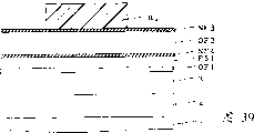
图39是表示与本发明有关的实施例4的半导体器件的制造工序的图。Fig. 39 is a diagram showing the manufacturing steps of the semiconductor device according to the fourth embodiment of the present invention.
图40是表示与本发明有关的实施例4的半导体器件的制造工序的图。Fig. 40 is a diagram showing the manufacturing steps of the semiconductor device according to the fourth embodiment of the present invention.
图41是表示与本发明有关的实施例4的半导体器件的制造工序的图。Fig. 41 is a diagram showing the manufacturing steps of the semiconductor device according to the fourth embodiment of the present invention.
图42是表示与本发明有关的实施例4的半导体器件的制造工序的图。Fig. 42 is a diagram showing the manufacturing process of the semiconductor device according to the fourth embodiment of the present invention.
图43是表示与本发明有关的实施例5的半导体器件的制造工序的图。Fig. 43 is a diagram showing the manufacturing process of the semiconductor device according to the fifth embodiment of the present invention.
图44是表示与本发明有关的实施例5的半导体器件的制造工序的图。Fig. 44 is a diagram showing the manufacturing process of the semiconductor device according to the fifth embodiment of the present invention.
图45是表示与本发明有关的实施例5的半导体器件的制造工序的图。Fig. 45 is a diagram showing the manufacturing steps of the semiconductor device according to the fifth embodiment of the present invention.
图46是表示与本发明有关的实施例5的半导体器件的变形例的制造工序的图。FIG. 46 is a diagram showing a manufacturing process of a modified example of the semiconductor device according to the fifth embodiment of the present invention.
图47是表示与本发明有关的实施例5的半导体器件的变形例的制造工序的图。FIG. 47 is a diagram showing a manufacturing process of a modified example of the semiconductor device according to the fifth embodiment of the present invention.
图48是表示与本发明有关的实施例5的半导体器件的变形例的制造工序的图。FIG. 48 is a diagram showing a manufacturing process of a modified example of the semiconductor device according to the fifth embodiment of the present invention.
图49是表示与本发明有关的实施例5的半导体器件的变形例的制造工序的图。FIG. 49 is a diagram showing a manufacturing process of a modified example of the semiconductor device according to the fifth embodiment of the present invention.
图50是表示与本发明有关的实施例5的半导体器件的变形例的制造工序的图。FIG. 50 is a diagram showing a manufacturing process of a modified example of the semiconductor device according to the fifth embodiment of the present invention.
图51是表示与本发明有关的实施例5的半导体器件的变形例的制造工序的图。FIG. 51 is a diagram showing a manufacturing process of a modified example of the semiconductor device according to the fifth embodiment of the present invention.
图52是表示与本发明有关的实施例5的半导体器件的变形例的制造工序的图。FIG. 52 is a diagram showing a manufacturing process of a modified example of the semiconductor device according to the fifth embodiment of the present invention.
图53是表示与本发明有关的实施例6的半导体器件的制造工序的图。Fig. 53 is a diagram showing the manufacturing steps of the semiconductor device according to the sixth embodiment of the present invention.
图54是表示与本发明有关的实施例6的半导体器件的制造工序的图。Fig. 54 is a diagram showing a manufacturing process of the semiconductor device according to the sixth embodiment of the present invention.
图55是表示与本发明有关的实施例6的半导体器件的制造工序的图。Fig. 55 is a diagram showing a manufacturing process of the semiconductor device according to the sixth embodiment of the present invention.
图56是表示与本发明有关的实施例6的半导体器件的制造工序的图。Fig. 56 is a diagram showing a manufacturing process of the semiconductor device according to the sixth embodiment of the present invention.
图57是表示与本发明有关的实施例6的半导体器件的制造工序的图。Fig. 57 is a diagram showing the manufacturing process of the semiconductor device according to the sixth embodiment of the present invention.
图58是表示与本发明有关的实施例7的半导体器件的制造工序的图。Fig. 58 is a diagram showing the manufacturing steps of the semiconductor device according to the seventh embodiment of the present invention.
图59是表示与本发明有关的实施例7的半导体器件的制造工序的图。Fig. 59 is a diagram showing the manufacturing steps of the semiconductor device according to the seventh embodiment of the present invention.
图60是表示与本发明有关的实施例7的半导体器件的制造工序的图。Fig. 60 is a diagram showing the manufacturing steps of the semiconductor device according to the seventh embodiment of the present invention.
图61是表示与本发明有关的实施例7的半导体器件的制造工序的图。Fig. 61 is a diagram showing a manufacturing process of the semiconductor device according to the seventh embodiment of the present invention.
图62是表示与本发明有关的实施例7的半导体器件的制造工序的图。Fig. 62 is a diagram showing the manufacturing steps of the semiconductor device according to the seventh embodiment of the present invention.
图63是表示与本发明有关的实施例7的半导体器件的制造工序的图。Fig. 63 is a diagram showing the manufacturing steps of the semiconductor device according to the seventh embodiment of the present invention.
图64是表示与本发明有关的实施例8的半导体器件的制造工序的图。Fig. 64 is a diagram showing the manufacturing steps of the semiconductor device according to the eighth embodiment of the present invention.
图65是表示与本发明有关的实施例8的半导体器件的制造工序的图。Fig. 65 is a diagram showing the manufacturing steps of the semiconductor device according to the eighth embodiment of the present invention.
图66是表示与本发明有关的实施例8的半导体器件的制造工序的图。Fig. 66 is a diagram showing the manufacturing steps of the semiconductor device according to the eighth embodiment of the present invention.
图67是表示与本发明有关的实施例8的半导体器件的制造工序的图。Fig. 67 is a diagram showing the manufacturing steps of the semiconductor device according to the eighth embodiment of the present invention.
图68是表示与本发明有关的实施例8的半导体器件的制造工序的图。Fig. 68 is a diagram showing the manufacturing steps of the semiconductor device according to the eighth embodiment of the present invention.
图69是表示与本发明有关的实施例8的半导体器件的制造工序的图。Fig. 69 is a diagram showing the manufacturing steps of the semiconductor device according to the eighth embodiment of the present invention.
图70是表示与本发明有关的实施例9的半导体器件的制造工序的图。Fig. 70 is a diagram showing the manufacturing steps of the semiconductor device according to the ninth embodiment of the present invention.
图71是表示与本发明有关的实施例9的半导体器件的制造工序的图。Fig. 71 is a diagram showing a manufacturing process of a semiconductor device according to Embodiment 9 of the present invention.
图72是表示与本发明有关的实施例9的半导体器件的制造工序的图。Fig. 72 is a diagram showing a manufacturing process of a semiconductor device according to Embodiment 9 of the present invention.
图73是表示与本发明有关的实施例9的半导体器件的制造工序的图。Fig. 73 is a diagram showing a manufacturing process of a semiconductor device according to Embodiment 9 of the present invention.
图74是表示与本发明有关的实施例9的半导体器件的制造工序的图。Fig. 74 is a diagram showing a manufacturing process of a semiconductor device according to Embodiment 9 of the present invention.
图75是表示与本发明有关的实施例9的半导体器件的制造工序的图。Fig. 75 is a diagram showing a manufacturing process of a semiconductor device according to Embodiment 9 of the present invention.
图76是表示与本发明有关的实施例9的半导体器件的制造工序的图。Fig. 76 is a diagram showing the manufacturing steps of the semiconductor device according to the ninth embodiment of the present invention.
图77是表示与本发明有关的实施例9的半导体器件的制造工序的图。Fig. 77 is a diagram showing the manufacturing steps of the semiconductor device according to the ninth embodiment of the present invention.
图78是表示与本发明有关的实施例9的半导体器件的制造工序的图。Fig. 78 is a diagram showing the manufacturing steps of the semiconductor device according to the ninth embodiment of the present invention.
图79是表示与本发明有关的实施例10的半导体器件的制造工序的图。Fig. 79 is a diagram showing the manufacturing steps of the semiconductor device according to the tenth embodiment of the present invention.
图80是表示与本发明有关的实施例10的半导体器件的制造工序的图。Fig. 80 is a diagram showing the manufacturing steps of the semiconductor device according to the tenth embodiment of the present invention.
图81是表示与本发明有关的实施例10的半导体器件的制造工序的图。Fig. 81 is a diagram showing the manufacturing steps of the semiconductor device according to the tenth embodiment of the present invention.
图82是表示具有场分离结构的半导体器件的整体结构的斜视图。Fig. 82 is a perspective view showing the overall structure of a semiconductor device having a field separation structure.
图83是表示现有的半导体器件的制造工序的图。FIG. 83 is a diagram showing a manufacturing process of a conventional semiconductor device.
图84是表示现有的半导体器件的制造工序的图。FIG. 84 is a diagram showing a manufacturing process of a conventional semiconductor device.
图85是表示现有的半导体器件的制造工序的图。FIG. 85 is a diagram showing a manufacturing process of a conventional semiconductor device.
图86是表示现有的半导体器件的制造工序的图。FIG. 86 is a diagram showing a manufacturing process of a conventional semiconductor device.
图87是表示现有的半导体器件的制造工序的图。FIG. 87 is a diagram showing a manufacturing process of a conventional semiconductor device.
图88是表示现有的半导体器件的制造工序的图。FIG. 88 is a diagram showing a manufacturing process of a conventional semiconductor device.
图89是表示现有的半导体器件的制造工序的图。FIG. 89 is a diagram showing a manufacturing process of a conventional semiconductor device.
图90是表示现有的半导体器件的制造工序的图。FIG. 90 is a diagram showing a manufacturing process of a conventional semiconductor device.
图91是表示现有的半导体器件的制造工序的图。FIG. 91 is a diagram showing a manufacturing process of a conventional semiconductor device.
图92是表示现有的半导体器件的制造工序的图。FIG. 92 is a diagram showing a manufacturing process of a conventional semiconductor device.
图93是表示现有的半导体器件的制造工序的图。FIG. 93 is a diagram showing a manufacturing process of a conventional semiconductor device.
图94是表示现有的半导体器件的制造工序的图。FIG. 94 is a diagram showing a manufacturing process of a conventional semiconductor device.
图95是表示现有的半导体器件的制造工序的图。FIG. 95 is a diagram showing a manufacturing process of a conventional semiconductor device.
图96是表示现有的半导体器件的制造工序的图。FIG. 96 is a diagram showing a manufacturing process of a conventional semiconductor device.
图97是表示现有的半导体器件的制造工序的图。FIG. 97 is a diagram showing a manufacturing process of a conventional semiconductor device.
图98是表示现有的半导体器件的制造工序的图。FIG. 98 is a diagram showing a manufacturing process of a conventional semiconductor device.
图99是表示现有的半导体器件的制造工序的图。FIG. 99 is a diagram showing a manufacturing process of a conventional semiconductor device.
图100是表示现有的半导体器件的制造工序的图。FIG. 100 is a diagram showing a manufacturing process of a conventional semiconductor device.
图101是表示现有的半导体器件的结构的图。FIG. 101 is a diagram showing the structure of a conventional semiconductor device.
<A.实施例1><
<A-1.器件结构><A-1. Device Structure>
作为与本发明有关的实施例1,一边利用图1~图9说明具有场分离结构的半导体器件M100的制造工序,一边说明关于半导体器件M100的结构和特征性的作用和效果。再有,由于半导体器件M100的基本结构与利用图82已说明的半导体器件M90相同,故对相同的构成部分标以相同的符号,不重复说明。此外,由于本发明涉及场分离结构,故在以后的说明中主要谈及场分离结构的构成。As a first embodiment of the present invention, the structure and characteristic actions and effects of the semiconductor device M100 will be described while describing the manufacturing process of the semiconductor device M100 having the field separation structure using FIGS. In addition, since the basic structure of the semiconductor device M100 is the same as that of the semiconductor device M90 described with reference to FIG. 82, the same reference numerals are assigned to the same components, and the description thereof will not be repeated. In addition, since the present invention relates to a field separation structure, the following description will mainly refer to the configuration of the field separation structure.
<A-2.制造方法><A-2. Manufacturing method>
首先,如图1所示,在用支撑衬底1和埋入氧化膜2构成的绝缘性衬底的SOI层3的表面上按顺序形成氧化硅膜OF1、掺了杂质(例如磷)的多晶硅层PS1、氮化硅膜NF1和氧化膜OF2,在氧化膜OF2上形成经图形刻蚀的抗蚀剂掩模R1。再有,在以后的说明中,将氧化硅膜称为氧化膜,将氮化硅膜称为氮化膜。First, as shown in FIG. 1, a silicon oxide film OF1, polysilicon doped with impurities (such as phosphorus) are sequentially formed on the surface of the
其中,利用热氧化法或CVD法形成厚度为200埃的氧化膜OF1,利用CVD法形成厚度为500埃的多晶硅层PS1,利用CVD法形成厚度为100埃的氮化膜NF1,利用CVD法形成厚度为1000埃的氧化膜OF2。再有,以上所述的各层的厚度是一例,氧化膜OF1的厚度可以在100~1000埃的范围内,多晶硅层PS1的厚度可以在500~1000埃的范围内,氮化膜NF1的厚度可以在100~1000埃的范围内,氧化膜OF2的厚度可以在500~2000埃的范围内。再有,多晶硅层PS1也可在首先利用CVD法形成了非多晶硅层之后,利用离子注入法导入杂质来形成。Among them, an oxide film OF1 with a thickness of 200 angstroms is formed by thermal oxidation or CVD, a polysilicon layer PS1 with a thickness of 500 angstroms is formed by CVD, and a nitride film NF1 with a thickness of 100 angstroms is formed by CVD. Oxide film OF2 with a thickness of 1000 angstroms. In addition, the thickness of each layer mentioned above is an example, the thickness of the oxide film OF1 can be in the range of 100-1000 angstroms, the thickness of the polysilicon layer PS1 can be in the range of 500-1000 angstroms, and the thickness of the nitride film NF1 The thickness of the oxide film OF2 may be in the range of 100-1000 angstroms, and the thickness of the oxide film OF2 may be in the range of 500-2000 angstroms. In addition, the polysilicon layer PS1 may be formed by introducing impurities by ion implantation after first forming a non-polysilicon layer by CVD.
然后,将抗蚀剂掩模R1作为掩模,利用各向异性刻蚀(干法刻蚀)有选择地除去氧化膜OF2,形成FS上部氧化膜41。Then, using the resist mask R1 as a mask, the oxide film OF2 is selectively removed by anisotropic etching (dry etching) to form the FS
其次,在图2中示出的工序中,除去抗蚀剂掩模R1,以FS上部氧化膜41为掩模,利用各向异性刻蚀(干法刻蚀)有选择地除去氮化膜NF1和多晶硅层PS1,形成FS上部氮化膜15(耐氧化性膜)和FS电极5。Next, in the process shown in FIG. 2, the resist mask R1 is removed, and the nitride film NF1 is selectively removed by anisotropic etching (dry etching) using the FS
其次,在图3中示出的工序中,利用CVD法形成氧化膜OF3,以便覆盖氧化膜OF1、FS上部氮化膜15、FS上部氧化膜41和FS电极5。再有,氧化膜OF3的厚度是1500~2000埃。Next, in the process shown in FIG. 3, oxide film OF3 is formed by CVD so as to cover oxide film OF1, FS
然后,在图4中示出的工序中,通过利用各向异性刻蚀(干法刻蚀)除去氧化膜OF3和OF1,在FS上部氮化膜15、FS上部氧化膜41和FS电极5的侧面形成侧壁氧化膜42,在FS电极5和侧壁氧化膜42的下部只留下氧化膜OF1,形成FS栅氧化膜43。再有,利用FS上部氧化膜41、侧壁氧化膜42、FS栅氧化膜43构成FS绝缘层4。Then, in the process shown in FIG. 4, by removing the oxide films OF3 and OF1 by anisotropic etching (dry etching), the FS
其次,在图5中示出的工序中,在SOI层3的表面上利用热氧化法形成作为栅氧化膜10的氧化膜OF4。在形成氧化膜OF4时,氧化剂、即氧通过侧壁氧化膜42、FS栅氧化膜43,将FS电极5的下面一侧进行氧化,但由于在FS电极5的上面形成了FS上部氮化膜15,所以FS电极5的上面一侧不会被氧化,这样就降低了由于氧化使FS电极5的实际厚度减少的比例。Next, in the process shown in FIG. 5 , an oxide film OF4 as
再有,利用到达了FS电极5的下部的氧,FS电极5的端部被氧化,呈向上方弯曲的形状。这是由于越接近端部被氧化的比例越多,越接近中央部被氧化的比例越小而引起的。此外,由于侧壁氧化膜42的下部的SOI层3也被氧化,故FS栅氧化膜43的端部的厚度增加。In addition, the end portion of the
其次,在图6中示出的工序中,利用CVD法在氧化膜OF4和FS绝缘层4的上部形成厚度为1000~1500埃的作为栅电极6的多晶硅层PS2。Next, in the process shown in FIG. 6, a polysilicon layer PS2 serving as the
其次,在图7中示出的工序中,利用各向异性刻蚀(干法刻蚀)有选择地除去多晶硅层PS2,形成栅电极6。然后,通过以栅电极6为掩模有选择地除去氧化膜OF4,形成栅氧化膜10。Next, in the process shown in FIG. 7, the polysilicon layer PS2 is selectively removed by anisotropic etching (dry etching), and the
此时,由于过刻蚀,也部分地除去FS上部氧化膜41,FS上部氧化膜41的厚度部分地变薄。在该状态下,在栅电极6的侧面形成用于在源·漏层内形成低掺杂漏层(以后称为LDD层)的侧壁氧化膜61。侧壁氧化膜61是这样来形成的,即在形成氧化膜以便覆盖栅电极6后,通过各向异性刻蚀(干法刻蚀)进行除去,在栅电极6的侧面以自对准的方式形成。此时,由于过刻蚀进一步除去FS上部氧化膜41。At this time, due to overetching, the FS
其次,在不打算形成硅化物层的部分上全面地形成硅化物保护膜11。硅化物保护膜11是在源·漏层的表面上形成硅化物层会产生器件工作方面的不良情况的半导体元件的源·漏层的表面上设置的一种膜。再有,关于硅化物保护膜,以后进一步进行说明。Next, the silicide
该形成方法是在衬底的整个面上形成了氧化膜后,通过各向异性刻蚀(干法刻蚀)有选择地除去氧化膜来覆盖规定的源·漏层的表面,但此时如图8所示,在FS绝缘层4的侧面(侧壁氧化膜42和FS栅氧化膜43的侧面)也以自对准的方式形成硅化物保护膜11。在形成该硅化物保护膜11时,由于过刻蚀进一步除去FS上部氧化膜41,FS上部氧化膜41部分地变得极薄。In this formation method, after an oxide film is formed on the entire surface of the substrate, the oxide film is selectively removed by anisotropic etching (dry etching) to cover the surface of the predetermined source/drain layer. As shown in FIG. 8, the silicide
但是,由于在FS电极5的上表面形成了FS上部氮化膜15,故即使FS上部氧化膜41在局部几乎被除去,FS电极5的上表面也不会露出。However, since the FS
在该状态下,如图9所示,以自对准的方式在栅电极6的上部表面和未图示的源·漏层的表面上形成例如800埃厚度的硅化物膜12。再有,硅化物膜12的形成方法如下,在多晶硅层或硅层的表面上淀积了例如钴(Co)等的金属薄膜后,在700℃的温度条件下进行热处理,使硅与金属反应而形成。In this state, as shown in FIG. 9 , a
作为硅化物膜12,可以是硅化钴(CoSi2)、硅化钛(TiSi2)或硅化镍(NiSi2)、硅化钨(WSi2)等中的任何一种。The
由于在氮化膜的表面上不形成硅化物膜,故如图9所示,在FS上部氮化膜15的表面上不会形成硅化物膜12。Since no silicide film is formed on the surface of the nitride film, as shown in FIG. 9, no
<A-3.特征性的作用和效果><A-3. Characteristic action and effect>
如上所述,在半导体器件M100中,由于能防止在FS电极5的表面上形成硅化物膜12,故可防止硅化物膜12剥离而成为导电性的粉尘,可防止残留在半导体器件上而对半导体器件的工作特性造成不良影响。此外,可防止伴随硅化物膜12的剥离而部分地丧失FS电极5而导致FS电极5的断线状态。As described above, in the semiconductor device M100, since the
再有,在防止形成硅化物膜12方面,在FS电极5的上部表面上设置的膜不限定于氮化膜,例如可使用氮氧化膜(SiON)。此外,也可使用氮化钛膜(TiN)、氮化钨(WN)。由于这些膜是导电性的,故也具有降低FS电极5的电阻值的作用。In addition, in order to prevent the formation of the
<A-4.变形例><A-4. Variation>
在利用图1~图9已说明的本发明的实施例1中,在图4中示出的工序中,说明了利用各向异性刻蚀(干法刻蚀)除去氧化膜OF3和OF1的例子,但也可用湿法刻蚀来除去氧化膜OF1。此时,通过事先将FS上部氧化膜41的宽度尺寸形成得比FS上部氮化膜15或FS电极5的宽度尺寸小,可得到以下说明的那种特征性的作用和效果。In
图10表示用于将FS上部氧化膜41的宽度尺寸形成得比FS上部氮化膜15或FS电极5的宽度尺寸小一些的工序的例子。如图10所示,将FS上部氧化膜41的宽度尺寸形成得比FS上部氮化膜15或FS电极5的宽度尺寸小一些,在其侧面形成淀积膜411。将FS上部氧化膜41和淀积膜411作为掩模,除去氮化膜NF1和多晶硅层PS1。其后,通过除去淀积膜411,可得到FS上部氧化膜41的宽度尺寸比FS上部氮化膜15或FS电极5的宽度尺寸小一些的结构。FIG. 10 shows an example of a process for forming the width dimension of the FS
这里,可有意识地形成淀积膜411,但也可利用在形成FS上部氧化膜41时的干法刻蚀中被使用的例如CF4等的刻蚀剂自然地被淀积的现象。即,在知道刻蚀剂在FS上部氧化膜41的侧面自然地淀积的情况下,可利用该现象。Here, the deposited
在图11中示出形成了氧化膜OF3以便覆盖氧化膜OF1、FS上部氮化膜15、FS上部氧化膜41、FS电极5的状态。11 shows a state where the oxide film OF3 is formed so as to cover the oxide film OF1, the FS
而且,如图12所示,利用干法刻蚀除去氧化膜OF3,使其达到规定的厚度。Then, as shown in FIG. 12, the oxide film OF3 is removed by dry etching to a predetermined thickness.
其次,在图13中示出的工序中,利用湿法刻蚀除去氧化膜OF3,同时也除去氧化膜OF1。湿法刻蚀以与形成OF3时的过程相反的方式进行。Next, in the process shown in FIG. 13, the oxide film OF3 is removed by wet etching, and the oxide film OF1 is also removed at the same time. Wet etching is performed in the reverse manner to the process used to form OF3.
即,一边反映具有台阶而构成的FS上部氧化膜41、FS上部氮化膜15、FS电极5的形状,一边生长氧化膜OF3。因而,在其轮廓形状方面存在平缓的台阶。在生长的同时,台阶消失,但作为过去的经历而留下来。利用湿法刻蚀来再现该起伏,如图13所示,在侧壁氧化膜的表面上形成平缓的台阶。That is, the oxide film OF3 is grown while reflecting the shapes of the FS
因此,由于在侧壁氧化膜42的表面上形成了平缓的台阶,故如使用图6已说明的那样,在形成作为栅电极的多晶硅层的情况下,多晶硅层的密接性良好,可解决栅电极剥离等问题。Therefore, since a gentle step is formed on the surface of the
此外,如图13中的区域A所示,由于FS栅氧化膜43的端部具有平缓的斜率,故与该部分为陡峭的情况相比,在以下方面有利。即,在以后的工序中在形成多晶硅层并有选择地进行刻蚀来形成栅电极的情况下(参照图7),在防止不需要的多晶硅层作为残渣留在该部分上这一点上效果很好,可减少由于多晶硅层残留而引起的短路的发生,可防止制造成品率的降低。In addition, as shown in the region A in FIG. 13 , since the end portion of the FS
<A-5.关于硅化物保护膜><A-5. About Silicide Protective Film>
这里,说明硅化物保护膜11。在图14中作为半导体集成电路的一例,示出了反相电路C2和保护该电路的保护电路C1。Here, the silicide
串联连接P沟道MOS晶体管P1和N沟道MOS晶体管N1来构成保护电路C1,在连接两者的节点ND1上连接着输入焊区PD。将P沟道MOS晶体管P1的栅电极连接到电源电位(Vcc),从而经常处于关断状态。将N沟道MOS晶体管N1的栅电极连接到接地电位,从而经常处于关断状态。A protection circuit C1 is formed by connecting a P-channel MOS transistor P1 and an N-channel MOS transistor N1 in series, and an input pad PD is connected to a node ND1 connecting them. The gate electrode of the P-channel MOS transistor P1 is connected to a power supply potential (Vcc) so as to be always in an off state. The gate electrode of the N-channel MOS transistor N1 is connected to the ground potential so as to be always in an off state.
串联连接P沟道MOS晶体管P2和N沟道MOS晶体管N2来构成反相电路C2,将两者的连接节点ND2连接到未图示的其他电路上。而且,将P沟道MOS晶体管P2和N沟道MOS晶体管N2的栅电极连接到保护电路C1的节点ND1。P-channel MOS transistor P2 and N-channel MOS transistor N2 are connected in series to form an inverter circuit C2, and a connection node ND2 between them is connected to another circuit not shown. Furthermore, the gate electrodes of the P-channel MOS transistor P2 and the N-channel MOS transistor N2 are connected to the node ND1 of the protection circuit C1.
这里,假定从输入焊区PD输入了浪涌(surge)电压的情况。由于浪涌电压是比通常的MOS晶体管的工作电压高的电压,故如果没有保护电路C1,则浪涌电压会加到反相电路C2的P沟道MOS晶体管P2和N沟道MOS晶体管N2的栅电极上,存在破坏两者的栅绝缘的担心。但是,由于保护电路C1的存在,如施加浪涌电压的话,在P沟道MOS晶体管P1和N沟道MOS晶体管N1的源·漏间发生击穿而流过电流,可防止浪涌电压加到反相电路C2上。Here, assume a case where a surge voltage is input from the input pad PD. Since the surge voltage is higher than the operating voltage of a normal MOS transistor, if there is no protection circuit C1, the surge voltage will be applied to the P-channel MOS transistor P2 and N-channel MOS transistor N2 of the inverter circuit C2. On the gate electrode, there is a possibility of destroying the gate insulation of both. However, due to the existence of the protection circuit C1, if a surge voltage is applied, a breakdown occurs between the sources and drains of the P-channel MOS transistor P1 and the N-channel MOS transistor N1, and a current flows, preventing the surge voltage from being applied to the circuit. on the inverting circuit C2.
由于保护电路C1以这种方式工作,故浪涌电压就加在源·漏间,这是需要硅化物保护膜的原因。Since the protection circuit C1 operates in this way, a surge voltage is applied between the source and the drain, which is the reason why the silicide protection film is required.
图15表示MOS晶体管的平面结构。MOS晶体管的结构是这样的:在中央部分配置细长形状的栅电极GE,在其短边方向的两个外侧配置源·漏区SD。一般来说,为了降低源·漏区SD与未图示的接触孔的接触电阻,在源·漏区SD的表面上形成硅化物膜SF,但在构成保护电路C1的MOS晶体管中,硅化物膜带来一些不良情况。FIG. 15 shows a planar structure of a MOS transistor. The structure of the MOS transistor is such that an elongated gate electrode GE is arranged in the central portion, and source/drain regions SD are arranged on both outer sides in the short side direction. Generally, the silicide film SF is formed on the surface of the source/drain region SD in order to reduce the contact resistance between the source/drain region SD and a contact hole (not shown), but in the MOS transistor constituting the protection circuit C1, the silicide film SF is Membranes bring about some undesirable situations.
在图16中示出了图15中所示的区域A的放大图。硅化物膜SF一般是多晶结构,如图16所示,由大小硅化物的晶粒GR构成。因而,在晶粒边界处反映各粒子的形状而具有起伏。在沿栅电极GE的端部的硅化物膜SF的端部处也是同样的情况,如图16所示,晶粒将栅电极GE夹在中间而对置。在这样的结构中,如果加上浪涌电压,则在栅电极GE的两侧的晶粒GR的突起部之间(箭头所示的间隙)引起浪涌电流的集中,故集中地破坏该部分,这样使MOS晶体管的工作发生故障,从而失去作为保护电路的功能。由于这个原因,在保护电路的源·漏区表面不形成硅化物膜,而代之以形成硅化物保护膜。An enlarged view of the area A shown in FIG. 15 is shown in FIG. 16 . The silicide film SF generally has a polycrystalline structure, and is composed of large and small silicide grains GR as shown in FIG. 16 . Therefore, the crystal grain boundary has undulations reflecting the shape of each particle. The same applies to the end portion of the silicide film SF along the end portion of the gate electrode GE. As shown in FIG. 16 , crystal grains are opposed to each other with the gate electrode GE sandwiched therebetween. In such a structure, when a surge voltage is applied, the surge current is concentrated between the protrusions of the crystal grains GR on both sides of the gate electrode GE (the gap indicated by the arrow), so that part is intensively destroyed. , so that the work of the MOS transistor fails, thereby losing its function as a protection circuit. For this reason, a silicide film is not formed on the surface of the source/drain region of the protection circuit, but a silicide protective film is formed instead.
但是,在保护电路以外的半导体集成电路、例如反相电路C2中,需要在源·漏区表面形成硅化物膜,因此,如上面所说明的那样,需要在形成硅化物膜之前有除去硅化物保护膜的工序。However, in semiconductor integrated circuits other than the protection circuit, such as the inverter circuit C2, it is necessary to form a silicide film on the surface of the source and drain regions. Therefore, as described above, it is necessary to remove the silicide film before forming the silicide film. The process of protective film.
<B.实施例2><B. Example 2>
<B-1.器件结构><B-1. Device Structure>
作为与本发明有关的实施例2,一边利用图17~图24说明具有场分离结构的半导体器件M200的制造工序,一边说明关于半导体器件M200的结构和特征性的作用和效果。再有,由于半导体器件M200的基本结构与利用图82已说明的半导体器件M90相同,故对相同的构成部分标以相同的符号,不重复说明。此外,由于本发明涉及场分离结构,故在以后的说明中主要谈及场分离结构的构成。As a second embodiment of the present invention, the structure and characteristic actions and effects of the semiconductor device M200 will be described while using FIGS. 17 to 24 to describe the manufacturing process of the semiconductor device M200 having the field separation structure. In addition, since the basic structure of the semiconductor device M200 is the same as that of the semiconductor device M90 described with reference to FIG. 82, the same reference numerals are assigned to the same components, and the description thereof will not be repeated. In addition, since the present invention relates to a field separation structure, the following description will mainly refer to the configuration of the field separation structure.
<B-2.制造方法><B-2. Manufacturing method>
首先,如图17中所示,在用支撑衬底1和埋入氧化膜2构成的绝缘性衬底的SOI层3的表面上按顺序形成氧化硅膜OF1、氮化膜NF2、掺了杂质(例如磷)的多晶硅层PS1、和氧化膜OF2,在氧化膜OF2上形成经图形刻蚀的抗蚀剂掩模R1。First, as shown in FIG. 17, a silicon oxide film OF1, a nitride film NF2, and an impurity-doped film are sequentially formed on the surface of the
其中,利用CVD法形成厚度为200埃的氮化膜NF2。再有,由于氧化硅膜OF1、多晶硅层PS1和氧化膜OF2的厚度和形成方法与利用实施例1说明过的厚度和形成方法相同,故省略其说明。Here, the nitride film NF2 is formed to a thickness of 200 angstroms by the CVD method. Since the thicknesses and formation methods of the silicon oxide film OF1, polysilicon layer PS1, and oxide film OF2 are the same as those described in
然后,在图18示出的工序中,将抗蚀剂掩模R1作为掩模,利用各向异性刻蚀(干法刻蚀)有选择地除去氧化膜OF2,形成FS上部氧化膜41。Then, in the process shown in FIG. 18 , the oxide film OF2 is selectively removed by anisotropic etching (dry etching) using the resist mask R1 as a mask to form the FS
其次,除去抗蚀剂掩模R1,以FS上部氧化膜41为掩模,利用各向异性刻蚀(干法刻蚀)有选择地除去多晶硅层PS1,形成FS电极5。Next, the resist mask R1 is removed, and the polysilicon layer PS1 is selectively removed by anisotropic etching (dry etching) using the FS
然后,在图19中示出的工序中,利用CVD法形成氧化膜OF3,以便覆盖氮化膜NF2、FS上部氧化膜41和FS电极5。再有,氧化膜OF3的厚度是1500~2000埃。Then, in the process shown in FIG. 19 , an oxide film OF3 is formed by the CVD method so as to cover the nitride film NF2 , the FS
然后,在图20中示出的工序中,通过利用各向异性刻蚀(干法刻蚀)除去氧化膜OF3,在FS上部氧化膜41和FS电极5的侧面形成侧壁氧化膜42。Then, in the process shown in FIG. 20, the oxide film OF3 is removed by anisotropic etching (dry etching), and the side
其次,在图21示出的工序中,对氮化膜NF2进行刻蚀,使其只在FS电极5和侧壁氧化膜42的下部留下,形成FS下部氮化膜16(耐氧化性膜)。再有,由于在氮化膜NF2的刻蚀中例如使用热磷酸进行的湿法刻蚀,故由于过刻蚀,FS下部氮化膜16的端部比侧壁氧化膜4的端部有一些收缩。Next, in the process shown in FIG. 21, the nitride film NF2 is etched to leave only the lower part of the
其次,在图22示出的工序中,对氧化膜OF1进行刻蚀,使其只在FS下部氮化膜16的下部留下,形成FS栅氧化膜43。再有,由于在氧化膜OF1的刻蚀中使用氢氟酸(HF)的湿法刻蚀,利用过刻蚀,FS栅氧化膜43的端部比FS下部氮化膜16的端部有一些收缩。再有,如果该收缩量大,则在以后的工序中形成栅电极时不需要的多晶硅层作为残渣而留下,故要尽可能缩短湿法刻蚀时间。为此,例如将氧化膜OF1的厚度设定为氮化膜NF2的一半、例如约100埃。Next, in the process shown in FIG. 22, the oxide film OF1 is etched to leave only the lower part of the FS
其次,如图23中所示,利用热氧化法在SOI层3的表面上形成作为栅氧化膜10的氧化膜OF4。在形成氧化膜OF4时,氧化剂、即氧通过侧壁氧化膜42、FS栅氧化膜43,但由于在FS电极5的下部形成了FS下部氮化膜16,故FS电极5的下面一侧不会氧化,可降低由于氧化而使FS电极5的实际厚度减少的比例。此外,由于不氧化FS电极5的端部,故可防止FS电极5呈向上方弯曲的形状。Next, as shown in FIG. 23, an oxide film OF4 as a
再有,虽然侧壁氧化膜42下部的SOI层3被氧化,但与FS电极5相比难以被氧化,此外,由于FS下部氮化膜16延伸到侧壁氧化膜42的下部,故FS栅氧化膜43的端部的厚度的增加变少。Furthermore, although the
其次,利用CVD法在氧化膜OF4和FS绝缘层4的上部形成作为栅电极6的多晶硅层PS2,利用各向异性刻蚀(干法刻蚀)有选择地除去多晶硅层PS2,形成栅电极6。然后,通过以栅电极6为掩模有选择地除去氧化膜OF4,形成栅氧化膜10。Next, form the polysilicon layer PS2 as the
此时,由于过刻蚀,也部分地除去FS上部氧化膜41,FS上部氧化膜41的厚度部分地变薄。在该状态下,在栅电极6的侧面形成用于在源·漏层内形成低掺杂漏层(以后称为LDD层)的侧壁氧化膜61。侧壁氧化膜61是这样形成的,即在形成氧化膜,以便覆盖栅电极6后,通过用各向异性刻蚀(干法刻蚀)进行除去,如图23所示,在栅电极6的侧面以自对准的方式形成。此时,由于过刻蚀进一步除去FS上部氧化膜41。At this time, due to overetching, the FS
其次,在整个面上形成硅化物保护膜11。然后,通过用各向异性刻蚀(干法刻蚀)有选择地除去,来覆盖规定的源·漏层的表面,但此时如图24所示,在侧壁氧化膜42、FS下部氮化膜16和FS栅氧化膜43的侧面也以自对准的方式形成硅化物保护膜11。在形成该硅化物保护膜11时虽然因过刻蚀进一步除去FS上部氧化膜41,但由于FS电极5是平坦的,故FS上部氧化膜41不会呈局部地变得极薄的状态、或局部地几乎被除去的状态。Next, a silicide
在这种状态下,在栅电极6的上部表面和未图示的源·漏层的表面上以自对准的方式形成厚度为800埃的硅化物膜12,但由于在氧化膜的表面上不形成硅化物膜,故如图24所示,在FS电极5的上表面不形成硅化物膜12。In this state, a
<B-3.特征性的作用和效果><B-3. Characteristic action and effect>
如上所述,在在半导体器件M200中,由于能防止在FS电极5的表面上形成硅化物膜12,故可防止硅化物膜12剥离而成为导电性的粉尘,可防止残留在半导体器件上而对半导体器件的工作特性造成不良影响。此外,可防止伴随硅化物膜12的剥离而部分地丧失FS电极5而导致FS电极5的断线状态。As described above, in the semiconductor device M200, since the
<B-4.变形例><B-4. Variation>
在利用图17~图24已说明的本发明的实施例2中,在图20中示出的工序中,说明了利用各向异性刻蚀(干法刻蚀)除去氧化膜OF3、在图21和图22示出的工序中,利用湿法刻蚀除去氮化膜NF2和氧化膜OF1的例子。此时,通过事先将FS上部氧化膜41的宽度尺寸形成得比FS电极5的宽度尺寸小,可得到以下说明的那种特征性的作用和效果。In
再有,由于在实施例1中利用图10说明了用于使上部氧化膜41的宽度尺寸形成得比FS电极5的宽度尺寸小的工序,故不再重复说明。In the first embodiment, since the steps for forming the
图25表示形成了氧化膜OF3,以便覆盖氮化膜41、FS上部氧化膜41和FS电极5的状态。FIG. 25 shows a state where the oxide film OF3 is formed so as to cover the
然后,如图26所示,利用干法刻蚀除去氧化膜OF3,直至达到预定的厚度。Then, as shown in FIG. 26, the oxide film OF3 is removed by dry etching until it reaches a predetermined thickness.
其次,在图27示出的工序中,对氮化膜NF2进行刻蚀,使其只在FS电极5和侧壁氧化膜42的下部留下,形成FS下部氮化膜16。再有,由于在氮化膜NF2的刻蚀中例如使用热磷酸的湿法刻蚀,故由于过刻蚀,FS下部氮化膜16的端部比侧壁氧化膜4的端部有一些收缩。Next, in the step shown in FIG. 27, the nitride film NF2 is etched to leave only the lower part of the
其次,在图28中示出的工序中,对氧化膜OF1进行刻蚀,使其只在FS下部氮化膜16的下部留下,形成FS栅氧化膜43。再有,由于在氧化膜OF1的刻蚀中例如使用氢氟酸(HF)的湿法刻蚀,由于过刻蚀,FS栅氧化膜43的端部比FS下部氮化膜16的端部有一些收缩。Next, in the process shown in FIG. 28, the oxide film OF1 is etched to leave only the lower part of the FS
该氧化膜的湿法刻蚀以与形成OF3时的过程相反的方式进行。由于这一点已在实施例1中说明过,故不再重复说明。由于氧化膜的湿法刻蚀,在侧壁氧化膜42的表面上反映出起因于FS上部氧化膜41的宽度尺寸与FS电极5的宽度尺寸的差异的台阶,形成平缓的台阶。Wet etching of this oxide film is performed in the reverse manner to the process for forming OF3. Since this point has been described in
这样一来,用图23已说明过,由于在侧壁氧化膜42的表面上形成了平缓的台阶,故在形成作为栅电极的多晶硅层的情况下,多晶硅层的密接性变得很好,可解决栅电极剥离等的问题。In this way, as described with reference to FIG. 23, since a gentle step is formed on the surface of the
<C.实施例3><C. Example 3>
<C-1.器件结构><C-1. Device Structure>
作为与本发明有关的实施例3,一边利用图29~图38说明具有场分离结构的半导体器件M300的制造工序,一边说明关于半导体器件M300的结构和特征性的作用和效果。再有,由于半导体器件M300的基本结构与利用图82已说明的半导体器件M90相同,故对相同的构成部分标以相同的符号,不重复说明。此外,由于本发明涉及场分离结构,故在以后的说明中主要谈及场分离结构的构成。As a third embodiment of the present invention, the structure and characteristic actions and effects of the semiconductor device M300 will be described while using FIGS. 29 to 38 to describe the manufacturing process of the semiconductor device M300 having the field separation structure. In addition, since the basic structure of the semiconductor device M300 is the same as that of the semiconductor device M90 described with reference to FIG. 82, the same reference numerals are assigned to the same components, and the description thereof will not be repeated. In addition, since the present invention relates to a field separation structure, the following description will mainly refer to the configuration of the field separation structure.
<C-2.制造方法><C-2. Manufacturing method>
首先,如图29中所示,在用支撑衬底1和埋入氧化膜2构成的绝缘性衬底的SOI层3的表面上按顺序形成氧化硅膜OF1、掺了杂质(例如磷)的多晶硅层PS1、氧化膜OF2、氮化膜NF3,在氮化膜NF3上形成经图形刻蚀的抗蚀剂掩模R1。First, as shown in FIG. 29 , on the surface of the
其中,利用热氧化法或CVD法形成厚度为200埃的氧化膜OF1,利用CVD法形成厚度为500埃的晶硅层PS1,利用CVD法形成厚度为1000埃的氧化膜OF2,利用CVD法形成厚度为100埃的氮化膜NF3。再有,以上示出的各层的厚度是一例,氮化膜NF3的厚度可以在100~1000埃的范围内。再有,由于其他膜的厚度的范围已在实施例1中说明过,故不再重复说明。Among them, an oxide film OF1 with a thickness of 200 angstroms is formed by thermal oxidation or CVD, a crystalline silicon layer PS1 with a thickness of 500 angstroms is formed by CVD, an oxide film OF2 with a thickness of 1000 angstroms is formed by CVD, and an oxide film OF2 with a thickness of 1000 angstroms is formed by CVD. Nitride film NF3 with a thickness of 100 angstroms. In addition, the thickness of each layer shown above is an example, and the thickness of the nitride film NF3 may be in the range of 100-1000 angstroms. In addition, since the thickness ranges of other films have already been described in Example 1, the description will not be repeated.
然后,在图30示出的工序中,将抗蚀剂掩模R1作为掩模,利用各向异性刻蚀(干法刻蚀)有选择地除去氮化膜NF3、氧化膜OF2、多晶硅层PS1,形成顶盖氮化膜17(第1耐氧化性膜)、FS上部氧化膜41、FS电极5。Then, in the process shown in FIG. 30, the nitride film NF3, the oxide film OF2, and the polysilicon layer PS1 are selectively removed by anisotropic etching (dry etching) using the resist mask R1 as a mask. , the cap nitride film 17 (first oxidation-resistant film), the FS
其次,除去抗蚀剂掩模R1,在图31中示出的工序中,利用CVD法形成氧化膜OF3,以便覆盖氧化膜OF1、顶盖氮化膜17、FS上部氧化膜41、FS电极5。再有,氧化膜OF3的厚度是1500~2000埃。Next, the resist mask R1 is removed, and in the process shown in FIG. . Furthermore, the thickness of the oxide film OF3 is 1500 to 2000 angstroms.
其次,图32中示出的工序中,利用各向异性刻蚀(干法刻蚀)除去氧化膜OF3,在顶盖氮化膜17、FS上部氧化膜41、FS电极5的侧面形成侧壁氧化膜42。Next, in the process shown in FIG. 32, the oxide film OF3 is removed by anisotropic etching (dry etching), and sidewalls are formed on the top
再有,使侧壁氧化膜42的厚度增加了相当于顶盖氮化膜17的厚度的部分。因而,可得到以下示出的氧化膜OF1的刻蚀中的刻蚀容限(margin)。Furthermore, the thickness of the side
其后,在图33中示出的工序中,除去氧化膜OF1。氧化膜OF1也是用于不使源·漏区暴露于干法刻蚀的等离子体中的保护膜,通过使用缓冲HF(氢氟酸)的湿法刻蚀将其除去。利用该工序,使OF3只在FS下部氮化膜16的下部留下,形成FS栅氧化膜43。再有,用FS上部氧化膜41、侧壁氧化膜42、FS栅氧化膜43构成FS绝缘层4。Thereafter, in the process shown in FIG. 33 , the oxide film OF1 is removed. The oxide film OF1 is also a protective film for preventing source/drain regions from being exposed to plasma of dry etching, and is removed by wet etching using buffered HF (hydrofluoric acid). In this step, OF3 is left only on the lower part of the FS
其中,利用缓冲HF来刻蚀氧化膜OF3和OF1,但由于用缓冲HF几乎不刻蚀氮化膜、即顶盖氮化膜17,故可防止FS上部氧化膜41的厚度减少。因而,可防止在以后的工序中在FS上部氧化膜41的上部形成的栅电极6和FS电极5之间的寄生电容的增大,此外,可充分地保证栅电极6和FS电极5之间的电绝缘。Among them, the buffer HF is used to etch the oxide films OF3 and OF1, but since the buffer HF hardly etches the nitride film, that is, the
此外,侧壁氧化膜42的厚度有一些减少,但本来由于侧壁氧化膜42的厚度是按多出顶盖氮化膜17的厚度的大小形成的,故通过该刻蚀而变成合适的厚度。再有,顶盖氮化膜17向FS上部氧化膜41的上表面突出的大小相当于侧壁氧化膜42收缩的这部分的大小。In addition, the thickness of the side
再有,缓冲HF(氢氟酸)是氢氟酸(HF)和氟化氨(NH4F)的混合水溶液,具有与稀氢氟酸相比氧化硅膜的刻蚀率变得稳定的特征。In addition, buffered HF (hydrofluoric acid) is a mixed aqueous solution of hydrofluoric acid (HF) and ammonium fluoride (NH 4 F), and has a characteristic that the etching rate of silicon oxide film becomes stable compared with dilute hydrofluoric acid. .
其次,在图34中示出的工序中,在SOI层3的表面上利用热氧化法形成作为栅氧化膜10的氧化膜OF4。在形成氧化膜OF4时,氧化剂、即氧通过侧壁氧化膜42、FS栅氧化膜43,而使FS电极5的下面一侧被氧化,但由于在FS电极5的上表面形成了顶盖氮化膜17,故可防止氧化剂从FS电极5的上面一侧侵入,可减少FS电极5的上面一侧被氧化的比例,可降低由于氧化而使FS电极5的实际厚度减少的比例。Next, in the process shown in FIG. 34 , an oxide film OF4 as
再有,FS电极5的端部被到达FS电极5的下部的氧所氧化,变成向上方弯曲的形状。这是因为越靠近端部被氧化的比例越多,越接近中央部分被氧化的比例越少之故。此外,由于侧壁氧化膜42下部的SOI层也被氧化,故FS栅氧化膜43的端部的厚度增加。In addition, the end portion of the
其次,在图35所示的工序中,利用CVD法在氧化膜OF4、顶盖氮化膜17和FS绝缘层4的上部形成厚度为1000~1500埃的作为栅电极6的多晶硅层PS2。Next, in the process shown in FIG. 35, a polysilicon layer PS2 serving as the
在图36中示出的工序中,利用各向异性刻蚀(干法刻蚀)有选择地除去多晶硅层PS2,形成栅电极6。此时,通过适当地选择刻蚀条件、例如刻蚀温度或刻蚀气体的种类,以使多晶硅层PF2相对于顶盖氮化膜17的刻蚀率增大,可防止顶盖氮化膜17的刻蚀,可防止FS上部氧化膜41的刻蚀。In the process shown in FIG. 36, the polysilicon layer PS2 is selectively removed by anisotropic etching (dry etching), and the
其次,通过以栅电极6为掩模有选择地除去氧化膜OF4,形成栅氧化膜10。Next,
其次,在栅电极6的侧面形成用于在源·漏层内形成低掺杂漏层(以后称为LDD层)的侧壁氧化膜61。侧壁氧化膜61是这样形成的,即在形成氧化膜以便覆盖栅电极6后,通过各向异性刻蚀(干法刻蚀)进行除去,如图23所示,在栅电极6的侧面以自对准的方式形成。Next, a
此时,通过选择刻蚀条件、例如选择氟化氢类的气体作为刻蚀气体,以使氧化膜相对于顶盖氮化膜17的刻蚀率增大,可防止顶盖氮化膜17的刻蚀,可防止FS上部氧化膜41的刻蚀。At this time, by selecting the etching conditions, for example, hydrogen fluoride gas is selected as the etching gas, so that the etching rate of the oxide film relative to the
其次,在图37中示出的工序中,在整个面上形成硅化物保护膜11。在该形成方法中,在衬底的整个面上形成了氧化膜后,通过用各向异性刻蚀(干法刻蚀)有选择地除去,来覆盖规定的源·漏层的表面,但此时如图38所示,在FS绝缘层4的侧面(侧壁氧化膜42和FS栅氧化膜43的侧面)也以自对准的方式形成硅化物保护膜11。在形成该硅化物保护膜11时通过选择刻蚀条件以使氧化膜相对于顶盖氮化膜17的刻蚀率增大,可防止顶盖氮化膜17的刻蚀,可防止FS上部氧化膜41的刻蚀。Next, in the process shown in FIG. 37, the silicide
在这种状态下,在栅电极6的上部表面和未图示的源·漏层的表面上以自对准的方式形成例如厚度为800埃的硅化物膜12,但在FS上部氧化膜41的上部形成了顶盖氮化膜17,不会发生FS上部氧化膜41部分地被除去而露出FS电极5的表面,不会在FS电极5的上表面形成硅化物膜12。In this state, a
再有,硅化物膜12的形成方法如下,在多晶硅层或硅层的表面上淀积了例如钴(Co)等的金属薄膜后,在700℃的温度条件下进行热处理,使硅与金属反应而形成。Furthermore, the formation method of the
<C-3.特征性的作用和效果><C-3. Characteristic action and effect>
如上所述,在半导体器件M300中,由于在FS上部氧化膜41的上表面形成了顶盖氮化膜17,故在制造过程中可防止FS上部氧化膜41的厚度减少,可防止栅电极6与FS电极5之间的寄生电容增大,可防止器件的工作速度的降低,此外,由于可充分保证栅电极6与FS电极5之间的电绝缘,故可防止这些电极间的短路故障。As described above, in the semiconductor device M300, since the
此外,由于顶盖氮化膜17的存在,可防止氧化剂从FS电极5的上面一侧侵入,可减少FS电极5的上面一侧被氧化的比例,可降低由于氧化而使FS电极5的实际厚度减少的比例,故可抑制FS电极5的电阻的增加。In addition, due to the existence of the top
此外,由于在半导体器件300中能防止在FS电极5的表面上形成硅化物膜12,故可防止硅化物膜12剥离而成为导电性的粉尘,可防止残留在半导体器件上对半导体器件的工作特性造成不良影响。此外,可防止伴随硅化物膜12的剥离而部分地丧失FS电极5而导致FS电极5的断线的状态,可在器件工作时得到充分的场分离效果。In addition, since the
<C-4.变形例><C-4. Variation>
在利用图29~图38说明过的本发明的实施例3中,虽然说明了用氮化膜作为顶盖氮化膜的例,但也可使用氮氧化膜(SiON)来代替氮化膜,可得到与上述同样的作用和效果。In
氮氧化膜是具有SiO2和Si3N4的中间性质的绝缘物,用CVD法、或Si3N4的热氧化来形成。The oxynitride film is an insulator having intermediate properties between SiO 2 and Si 3 N 4 , and is formed by CVD or thermal oxidation of Si 3 N 4 .
<D.实施例4><
<D-1.器件结构><D-1. Device Structure>
作为与本发明有关的实施例4,一边利用图39~图42说明具有场分离结构的半导体器件M400的制造工序,一边说明半导体器件M400的结构和特征性的作用和效果。再有,由于半导体器件M400的基本结构与利用图82说明过的半导体器件M90相同,故对相同的构成部分标以相同的符号,不再重复说明。此外,由于本发明涉及场分离结构,故在以后的说明中主要谈及场分离结构的构成。As a fourth embodiment of the present invention, the structure and characteristic actions and effects of the semiconductor device M400 will be described while using FIGS. 39 to 42 to describe the manufacturing process of the semiconductor device M400 having the field separation structure. In addition, since the basic structure of the semiconductor device M400 is the same as that of the semiconductor device M90 described with reference to FIG. 82, the same components are given the same reference numerals, and the description thereof will not be repeated. In addition, since the present invention relates to a field separation structure, the following description will mainly refer to the configuration of the field separation structure.
此外,关于与利用图29~图38说明过的本发明的实施例3相同的构成部分,标以相同的符号,不再重复说明。In addition, the same reference numerals are assigned to the same components as those in
<D-2.制造方法><D-2. Manufacturing method>
首先,如图39中所示,在用支撑衬底1和埋入氧化膜2构成的绝缘性衬底的SOI层3的表面上按顺序形成氧化硅膜OF1、氮化膜NF4、掺了杂质(例如磷)的多晶硅层PS1、氧化膜OF2、氮化膜NF3,在氮化膜NF3上形成经图形刻蚀的抗蚀剂掩模R1。First, as shown in FIG. 39, a silicon oxide film OF1, a nitride film NF4, and an impurity-doped film are sequentially formed on the surface of the
其中,利用CVD法形成厚度为100埃的氮化膜NF3和NF4。再有,上述氮化膜NF3和NF4的厚度是一例,可以在100~1000埃的范围内。再有,由于其他膜的厚度的范围已在实施例1中说明过,故不再重复说明。Here, the nitride films NF3 and NF4 are formed to a thickness of 100 angstroms by CVD. Incidentally, the thicknesses of the above-mentioned nitride films NF3 and NF4 are an example, and may be within a range of 100 to 1000 angstroms. In addition, since the thickness ranges of other films have already been described in Example 1, the description will not be repeated.
然后,将抗蚀剂掩模R1作为掩模,利用各向异性刻蚀(干法刻蚀)有选择地除去氮化膜NF3、氧化膜OF2、氮化膜NF4、多晶硅层PS1,形成顶盖氮化膜17(第1耐氧化性膜)、FS上部氧化膜41、FS上部氮化膜18(第2耐氧化性膜)、FS电极5。Then, using the resist mask R1 as a mask, the nitride film NF3, the oxide film OF2, the nitride film NF4, and the polysilicon layer PS1 are selectively removed by anisotropic etching (dry etching) to form a cap. Nitride film 17 (first oxidation resistant film), FS
其次,除去抗蚀剂掩模R1,利用CVD法形成厚度为1500~2000埃的氧化膜,以便覆盖氧化膜OF1、顶盖氮化膜17、FS上部氧化膜41、FS上部氮化膜18、FS电极5。其后,利用各向异性刻蚀(干法刻蚀)除去该氧化膜,在顶盖氮化膜17、FS上部氧化膜41、FS上部氮化膜18、FS电极5的侧面形成侧壁氧化膜42。Next, remove the resist mask R1, and form an oxide film with a thickness of 1500 to 2000 angstroms by CVD to cover the oxide film OF1, the top
再有,使侧壁氧化膜42的厚度增加了相当于顶盖氮化膜17和FS上部氮化膜18的厚度的部分。因而,可得到以下所述的氧化膜OF1的刻蚀中的刻蚀容限。Furthermore, the thickness of the side
其后,在图41中示出的工序中,除去氧化膜OF1。氧化膜OF1也是用于不使源·漏区暴露于干法刻蚀的等离子体中的保护膜,通过使用缓冲HF(氢氟酸)的湿法刻蚀将其除去。利用该工序,使OF3只在FS下部氮化膜16的下部留下,形成FS栅氧化膜43。再有,用FS上部氧化膜41、侧壁氧化膜42、FS栅氧化膜43构成FS绝缘层4。Thereafter, in the process shown in FIG. 41 , the oxide film OF1 is removed. The oxide film OF1 is also a protective film for preventing source/drain regions from being exposed to plasma of dry etching, and is removed by wet etching using buffered HF (hydrofluoric acid). In this step, OF3 is left only on the lower part of the FS
其中,利用缓冲HF来刻蚀氧化膜OF3和OF1,但由于用缓冲HF几乎不刻蚀氮化膜、即顶盖氮化膜17,故可防止FS上部氧化膜41的厚度减少。因而,可防止在以后的工序中在FS上部氧化膜41的上部形成的栅电极6和FS电极5之间的寄生电容的增大,此外,可充分地保证栅电极6和FS电极5之间的电绝缘。Among them, the buffer HF is used to etch the oxide films OF3 and OF1, but since the buffer HF hardly etches the nitride film, that is, the
此外,侧壁氧化膜42的厚度有一些减少,但本来由于侧壁氧化膜42的厚是按多出顶盖氮化膜17的厚度的大小形成的,故通过该刻蚀而变成合适的厚度。再有,顶盖氮化膜17向FS上部氧化膜41的上表面突出的大小相当于侧壁氧化膜42收缩的这部分的大小。In addition, the thickness of the side
其次,利用热氧化法在SOI层3的表面上形成作为栅氧化膜10的氧化膜。在形成该氧化膜时,氧化剂、印氧通过侧壁氧化膜42、而使FS栅氧化膜43,FS电极5的下面一侧被氧化,但由于在FS上部氧化膜41上形成了顶盖氮化膜17,再在FS电极5的上表面形成了FS上部氮化膜18,故可防止氧化剂从FS电极5的上面一侧侵入,例如即使氧化剂侵入,也可防止FS电极5的上表面一侧被氧化。Next, an oxide film as
再有,FS电极5的端部被到达FS电极5的下部的氧所氧化,变成向上方弯曲的形状。这是因为越靠近端部被氧化的比例越多,越接近中央部分被氧化的比例越少之故。此外,由于侧壁氧化膜42下部的SOI层也被氧化,故FS栅氧化膜43的端部的厚度增加。In addition, the end portion of the
以后的工序与本发明的实施例3中利用图35~图38说明过的工序相同,经过有选择地形成栅电极6的工序、在栅电极6的侧壁形成侧壁氧化膜61的工序、有选择地形成硅化物保护膜11的工序、有选择地形成硅化物膜12的工序后,得到图42中示出的半导体器件M400。Subsequent steps are the same as the steps described with reference to FIGS. After the step of selectively forming the silicide
<D-3.特征性的作用和效果><D-3. Characteristic action and effect>
如上所述,在半导体器件M400中,由于顶盖氮化膜17的存在,故关于防止FS上部氧化膜41的厚度减少和防止在FS电极5的表面上形成硅化物膜12的作用和效果与实施例3相同,但由于在FS电极5的上表面形成了FS上部氮化膜18,可减少FS电极5的上表面一侧被氧化,可进一步降低由于氧化而使FS电极5的实际厚度减少的比例。As described above, in the semiconductor device M400, due to the presence of the
另外,在顶盖氮化膜和FS上部氮化膜中,不用说可使用氮氧化膜(SiON)来代替氮化膜。In addition, in the cap nitride film and the FS upper nitride film, it goes without saying that an oxynitride film (SiON) may be used instead of the nitride film.
<E.实施例5><
<E-1.器件结构><E-1. Device Structure>
作为与本发明有关的实施例5,一边利用图43~图45说明具有场分离结构的半导体器件MS00的制造工序,一边说明半导体器件M500的结构和特征性的作用和效果。再有,关于与利用图29~图38说明过的本发明的实施例3相同的构成部分,标以相同的符号,不再重复说明。As a fifth embodiment of the present invention, the structure and characteristic functions and effects of the semiconductor device M500 will be described while using FIGS. 43 to 45 to describe the manufacturing process of the semiconductor device MS00 having the field separation structure. 29 to 38 are used to denote the same components as in
<E-2.制造方法><E-2. Manufacturing method>
在图43示出的工序中,通过从顶盖氮化膜17(第1耐氧化性膜)和FS绝缘膜4的上部进行氮(N)离子的注入,如图44所示,至少在侧壁氧化膜42的表面上形成接近于氮化膜的结构的侧壁保护膜19(第2耐氧化性膜)。再有,由于到图43中示出的结构为止的工序与实施例3中用图29~图33说明过的工序相同,故不再重复说明。In the process shown in FIG. 43, nitrogen (N) ions are implanted from the top of the cap nitride film 17 (first oxidation-resistant film) and the
这里,氮(N)离子的注入条件为,能量是20~60keV,注入后的密度为1×10¹⁴~1×10²⁰/cm3。这样形成的侧壁保护膜19与氮化膜相同,具有妨碍氧通过的特性。Here, nitrogen (N) ions are implanted under conditions such that the energy is 20 to 60 keV, and the implanted density is 1×10 14 to 1×10 20 /cm 3 . The sidewall protective film 19 formed in this way has the property of preventing the passage of oxygen, similarly to the nitride film.
其次,在SOI层3的表面上利用热氧化法形成作为栅氧化膜10的氧化膜,在该氧化膜的形成时,由于作为氧化剂的氧不能通过顶盖氮化膜17和侧壁保护膜19,故不氧化FS电极5的上表面一侧和下表面一侧。氧只是从FS栅氧化膜43的端部的侧面侵入,但其量很少,不会氧化FS电极5。Next, on the surface of the
再有,除了来自上方的氮离子的注入以外,也从斜方向注入氮离子,在FS栅氧化膜43的端部侧面也形成接近于氮化膜的结构的保护膜,尽可能地防止氧的侵入,可防止FS电极5的氧化。Furthermore, in addition to the implantation of nitrogen ions from above, nitrogen ions are also implanted from an oblique direction to form a protective film with a structure close to that of a nitride film on the side of the end of the FS
因而,可防止FS电极5的端部呈向上方弯曲的形状,同时可防止FS电极5的实际厚度减少。Therefore, the end portion of the
以后的工序与本发明的实施例3中利用图35~图38说明过的工序相同,经过有选择地形成栅电极6的工序、在栅电极6的侧壁形成侧壁氧化膜61的工序、有选择地形成硅化物保护膜11的工序后、有选择地形成硅化物膜12的工序,得到图45中示出的半导体器件M500。Subsequent steps are the same as the steps described with reference to FIGS. After the step of selectively forming the silicide
<E-3.特征性的作用和效果><E-3. Characteristic action and effect>
如上所述,在半导体器件M500中,由于顶盖氮化膜17的存在,故关于防止FS上部氧化膜41的厚度减少的作用和效果和防止在FS电极5的表面上形成硅化物膜12的作用和效果与实施例3相同,但由于顶盖氮化膜17和侧壁保护膜19的存在,可得到以下所述的进一步的作用和效果。As described above, in the semiconductor device M500, due to the presence of the
即,由于可防止氧化FS电极5的上表面一侧和下表面一侧和可防止FS电极5的端部呈向上方弯曲的形状,故可防止与栅电极6的距离部分地变窄、导致与栅电极6之间的寄生电容的增大或绝缘破坏。That is, since the upper surface side and the lower surface side of the
此外,由于可防止因氧化FS电极5的实际厚度减少,故可防止FS电极5的电阻增加。In addition, since the actual thickness of the
此外,由于侧壁保护膜19的存在,可防止在栅电极6的形成工序、侧壁侧壁氧化膜61的形成工序、硅化物保护膜11的形成工序中因过刻蚀而部分地除去侧壁氧化膜42。In addition, due to the existence of the sidewall protection film 19, it is possible to prevent the sidewall from being partially removed due to overetching in the formation process of the
<E-4.变形例1><E-4.
在以上已说明的实施例5中,说明了利用氮离子注入而在侧壁氧化膜42的表面上形成接近于氮化膜的结构的侧壁保护膜19的例子,但也可在侧壁氧化膜42的表面上形成用氮化膜构成的侧壁表面氮化膜20(第2耐氧化性膜)来代替侧壁保护膜19。In
现用图46~图48说明其一例。首先,如图46所示,在FS上部氧化膜41和FS电极5的侧面形成侧壁氧化膜42。此时,考虑到以后形成的侧壁氮化膜20的厚度,不使侧壁氧化膜42完全覆盖FS上部氧化膜41的侧面。再有,由于到图46中示出的结构为止的工序与在实施例3中利用图29~图32说明过的工序相同,故不再重复说明。An example thereof will now be described with reference to FIGS. 46 to 48 . First, as shown in FIG. 46 ,
其次,在图47中示出的工序中,在侧壁氧化膜42的表面上形成用氮化膜构成的侧壁表面氮化膜20。利用CVD法在整个表面上形成例如厚度为1000埃的侧壁表面氮化膜20之后,通过各向异性刻蚀除去侧壁氧化膜42的表面以外的氮化膜,可得到侧壁表面氮化膜20。Next, in the process shown in FIG. 47 , the sidewall
其后,在图48中示出的工序中,通过使用缓冲HF(氢氟酸)的湿法刻蚀除去氧化膜OF1。通过该工序,只在FS电极5和侧壁氧化膜42的下部留下氧化膜OF1,成为FS栅氧化膜43。Thereafter, in the process shown in FIG. 48 , the oxide film OF1 is removed by wet etching using buffered HF (hydrofluoric acid). Through this process, only the oxide film OF1 is left on the lower part of the
利用缓冲HF来刻蚀氧化膜OF1,但由于缓冲HF几乎不刻蚀氮化膜、即顶盖氮化膜17和侧壁表面氮化膜20,故可防止FS上部氧化膜41和侧壁氧化膜42的厚度减少。Utilize buffer HF to etch the oxide film OF1, but because the buffer HF hardly etches the nitride film, that is, the top
<E-5.变形例2><E-5.
再有,在以上的说明中,说明了在侧壁表面氮化膜20的形成中形成厚度约为1000埃的氮化膜的例子,但氮化膜的厚度可以更薄。In addition, in the above description, an example was described in which a nitride film with a thickness of about 1000 angstroms was formed in the formation of the
利用图49~图52说明其一例。首先,如图49所示,在顶盖氮化膜17、FS上部氧化膜41和FS电极5的侧面形成侧壁氧化膜(第2氧化膜)42A。再有,由于到图49中示出的结构为止的工序与在实施例3中利用图29~图32说明过的工序大体相同,故不再重复说明。但是,这种情况的侧壁氧化膜42A与实施例1~4中已说明的侧壁氧化膜42相比,其厚度形成得较薄。An example thereof will be described with reference to FIGS. 49 to 52 . First, as shown in FIG. 49 , a side wall oxide film (second oxide film) 42A is formed on the side surfaces of the
其次,在图50中示出的工序中,利用CVD法在整个面上形成例如厚度约为200~300埃的氮化膜NF5。Next, in the step shown in FIG. 50, a nitride film NF5 having a thickness of, for example, about 200 to 300 angstroms is formed on the entire surface by CVD.
其后,在图51中示出的工序中,通过各向异性刻蚀除去侧壁氧化膜42A的表面以外的氮化膜NF5,可得到侧壁表面氮化膜20A(第2耐氧化性膜)。Thereafter, in the process shown in FIG. 51, the nitride film NF5 other than the surface of the
其后,在图52中示出的工序中,通过使用缓冲HF(氢氟酸)的湿法刻蚀除去氧化膜OF1。通过该工序,只在FS电极5和侧壁氧化膜42A的下部留下氧化膜OF1,成为FS栅氧化膜43。Thereafter, in the process shown in FIG. 52, the oxide film OF1 is removed by wet etching using buffered HF (hydrofluoric acid). Through this process, only the oxide film OF1 remains on the lower part of the
这里,利用缓冲HF来刻蚀氧化膜OF1,但由于缓冲HF几乎不刻蚀氮化膜、即顶盖氮化膜17和侧壁表面氮化膜20A,故可防止FS上部氧化膜41和侧壁氧化膜42A的厚度减少。Here, the buffer HF is used to etch the oxide film OF1, but since the buffer HF almost does not etch the nitride film, that is, the top
<F.实施例6><
<F-1.器件结构><F-1. Device Structure>
作为与本发明有关的实施例6,一边利用图53~图57说明具有场分离结构的半导体器件M600的制造工序,一边说明半导体器件M600的结构和特征性的作用和效果。再有,由于半导体器件M600的基本的结构与利用图82说明过的半导体器件M90相同,故对相同的构成部分标以相同的符号,不再重复说明。此外,由于本发明涉及场分离结构,故在以后的说明中主要谈及场分离结构的构成。As a sixth embodiment of the present invention, the structure and characteristic actions and effects of the semiconductor device M600 will be described while using FIGS. 53 to 57 to describe the manufacturing process of the semiconductor device M600 having the field separation structure. In addition, since the basic structure of the semiconductor device M600 is the same as that of the semiconductor device M90 described with reference to FIG. 82, the same reference numerals are assigned to the same components, and the description thereof will not be repeated. In addition, since the present invention relates to a field separation structure, the following description will mainly refer to the configuration of the field separation structure.
<F-2.制造方法><F-2. Manufacturing method>
首先,如图53所示,在用支撑衬底1和埋入氧化膜2构成的绝缘性衬底的SOI层3的表面上按顺序形成氮化膜NF6、掺了杂质(例如磷)的多晶硅层PS1、氮化膜NF7,在氮化膜NF7上形成经图形刻蚀的抗蚀剂掩模R1。First, as shown in FIG. 53, on the surface of the
其中,利用CVD法形成厚度分别为200埃和300埃的氮化膜NF6和NF7。再有,氮化膜NF6和NF7的厚度可以在100~1000埃的范围内。再有,由于多晶硅层PS1的厚度和形成方法已在实施例1中说明过,故省略其说明。Among them, the nitride films NF6 and NF7 are formed by CVD method with thicknesses of 200 angstroms and 300 angstroms, respectively. Further, the thickness of the nitride films NF6 and NF7 may be in the range of 100 to 1000 angstroms. Note that, since the thickness and formation method of the polysilicon layer PS1 have already been described in
其次,在图54示出的工序中,有选择地除去氮化膜NF7和多晶硅层PS1。形成FS上部氮化膜21(第1耐氧化性膜)和FS电极5。这里,之所以留下氮化膜NF6,是为了减少因刻蚀而引起的SOI层3的损伤。Next, in the process shown in FIG. 54, the nitride film NF7 and the polysilicon layer PS1 are selectively removed. The FS upper nitride film 21 (first oxidation-resistant film) and the
其次,在除去抗蚀剂掩模R1后,在图55中示出的工序中,利用CVD法形成氮化膜NF8,以便覆盖氮化膜NF6、FS上部氮化膜21和FS电极5。Next, after removing the resist mask R1, in the process shown in FIG. 55, a nitride film NF8 is formed by CVD so as to cover the nitride film NF6, the FS
其次,图56中示出的工序中,利用各向异性刻蚀除去氮化膜NF6和NF7,在FS上部氮化膜21和FS电极5的侧面形成侧壁氮化膜22(第2耐氧化性膜),在侧壁氮化膜22和FS电极5的下部形成FS栅氮化膜23。Next, in the process shown in FIG. 56, the nitride films NF6 and NF7 are removed by anisotropic etching, and the side wall nitride film 22 (the second oxidation resistant film 22) is formed on the side surfaces of the FS
此时,由于过刻蚀而挖去侧壁氮化膜22的端部附近的SOI层3的一部分,形成凹部DP。再有,由FS上部氮化膜21、侧壁氮化膜22和FS栅氮化膜23形成FS绝缘膜4A。At this time, a part of the
其次,在SOI层3的表面上形成栅氧化膜之前,利用湿法刻蚀除去在SOI层3的表面上形成的自然氧化膜,但此时如使用缓冲HF作为刻蚀剂,则氧化膜虽被刻蚀,但缓冲HF几乎不刻蚀氮化膜、即FS绝缘膜4A(FS上部氮化膜21、侧壁氮化膜22和FS栅氮化膜23),故可防止FS绝缘膜4A的厚度减少。Next, before forming the gate oxide film on the surface of the
因此,可防止侧壁氮化膜22收缩从而在侧壁氮化膜22的周围形成边缘部分,可防止起因于边缘部分而发生的栅氧化膜的破损,可提高栅氧化膜的可靠性。Therefore, it is possible to prevent
此外,由于用氮化膜覆盖了FS电极5,故不受上述湿法刻蚀的影响,可防止FS电极5的厚度变薄。In addition, since the
再有,在形成侧壁氮化膜22后,即在干法刻蚀后,可在氮气(N2)的气氛下在600~1200℃的范围内进行10~60分的电炉退火。此外,可将在1000~1200℃的范围内进行的10~60秒的短时间退火和上述电炉退火结合起来。该退火的目的在于消除伴随侧壁氮化膜22的形成而在衬底表面引起的刻蚀损伤。Furthermore, after the
此外,在除去刻蚀损伤方面,也可进行以CF4为主要成分的化学干法刻蚀,以将SOI层3的表面刻去约10~300埃。通常在该化学刻蚀中,一边刻蚀硅,一边淀积氧化硅膜,这样来进行刻蚀。因此,需要对已淀积的氧化硅膜进行湿法刻蚀的工序,但由于FS绝缘膜4A对于缓冲HF等刻蚀剂具有抗刻蚀性,故不被除去。In addition, in terms of removing etching damage, chemical dry etching with CF 4 as the main component can also be performed to etch away about 10-300 angstroms from the surface of the
其次,在SOI层3的表面上利用热氧化法形成作为栅氧化膜10的氧化膜。在形成该氧化膜时,由于氧化剂、即氧不能通过FS上部氮化膜21、侧壁氮化膜22和FS栅氮化膜23,故FS电极5的上表面一侧和下表面一侧不被氧化。Next, an oxide film as
因而,可防止FS电极5的端部呈向上方弯曲的形状,同时可防止FS电极5的实际厚度减少。Therefore, the end portion of the
以后的工序与本发明的实施例3中利用图35~图38说明过的工序相同,经过有选择地形成栅电极6的工序、在栅电极6的侧壁形成侧壁氧化膜61的工序、有选择地形成硅化物保护膜11的工序、有选择地形成硅化物膜12的工序后,得到图57中示出的半导体器件M600。Subsequent steps are the same as the steps described with reference to FIGS. After the step of selectively forming the silicide
再有,在以上的说明中,将FS上部氮化膜21的厚度定为300埃,但在有必要降低与栅电极6之间的寄生电容或防止绝缘破坏的情况下,也可将该厚度定为1000埃。In addition, in the above description, the thickness of the
再有,在上述各工序中,必须防止对FS上部氮化膜21的过刻蚀。即,在形成栅电极6时,选择刻蚀条件,以便增大栅电极材料(多晶硅)相对于FS上部氮化膜21的刻蚀率,在形成侧壁氧化膜61时,选择刻蚀条件,以便增氧化膜相对于FS上部氮化膜21的刻蚀率,在形成硅化物保护膜11时,选择刻蚀条件,以便增大氧化膜相对于FS上部氮化膜21的刻蚀率。In addition, in each of the above steps, it is necessary to prevent over-etching of the
<F-3.特征性的作用和效果><F-3. Characteristic action and effect>
如上所述,在半导体器件M600中,由于用氮化膜构成了FS绝缘膜4A,故在利用湿法刻蚀除去自然氧化膜时,可防止侧壁氮化膜22收缩从而在侧壁氮化膜22的周围形成边缘部分,可防止起因于边缘部分而发生的栅氧化膜的破损,可提高栅氧化膜的可靠性。As described above, in the semiconductor device M600, since the
此外,在形成栅氧化膜10时,由于氧化剂、即氧,不能通过FS上部氮化膜21、侧壁氮化膜22和FS栅氮化膜23,故FS电极5的上表面一侧和下表面一侧不被氧化,可防止FS电极5的端部呈向上方弯曲的形状,因此可防止与栅电极的距离部分地变窄,可防止与栅电极6之间的寄生电容的增大或导致绝缘破坏。In addition, when the
此外,由于可防止因氧化而使FS电极5的实际厚度减少,故可防止FS电极5的电阻增加。In addition, since the actual thickness reduction of the
此外,由于在FS电极5的上部形成了FS上部氮化膜21,故在栅电极6的形成工序、侧壁氧化膜61的形成工序、硅化物保护膜11的形成工序中,通过分别选择前面已说明的那种刻蚀条件,可防止因过刻蚀而除去FS上部氮化膜21,可防止栅电极6与FS电极5之间的寄生电容增大,可防止器件的工作速度降低,此外,由于可充分保证栅电极6与FS电极5之间的电绝缘,故可防止这些电极间的短路故障。In addition, since the FS
此外,通过选择上述刻蚀条件,在栅电极6的形成工序、侧壁氧化膜61的形成工序、硅化物保护膜11的形成工序中,可防止因过刻蚀而部分地除去侧壁氮化膜22。In addition, by selecting the above-mentioned etching conditions, in the formation process of the
此外,由于可防止FS电极5露出,可防止在FS电极5的表面上形成硅化物膜12,故可防止硅化物膜12剥离而成为导电性的粉尘,可防止残留在半导体器件上而对半导体器件的工作特性造成不良影响。此外,可防止伴随硅化物膜12的剥离而部分地丧失FS电极5而导致FS电极5的断线的状态,可在器件工作时得到充分的场分离效果。In addition, since the exposure of the
<F-4.变形例><F-4. Variation>
在以上已说明的本发明的实施例6中,在利用图54和图55的说明中,说明了利用抗蚀剂掩模R1同时形成FS上部氮化膜22和FS电极5的例子,但也可用抗蚀剂掩模R1只对FS上部氮化膜22进行图形刻蚀,对于剩下的膜可以FS上部氮化膜22为掩模进行图形刻蚀。In
通过这样做,可减少使用抗蚀剂掩模R1的情况下产生的不良情况。即,如果使用抗蚀剂掩模R1,则发生从抗蚀剂掩模R1放出的杂质附着于其下部的膜的侧壁上,致使该膜的厚度尺寸变大的现象。如在多层中重复该现象,则存在多层结构的剖面形状变成阶梯状,从而不能正确地反映抗蚀剂掩模R1的形状的可能性。但是,通过限制抗蚀剂掩模R1的使用,可减少这样的不良情况的发生。By doing so, it is possible to reduce defects that occur when the resist mask R1 is used. That is, when the resist mask R1 is used, impurities released from the resist mask R1 adhere to the sidewall of the film below it, and the thickness dimension of the film becomes large. If this phenomenon is repeated in multiple layers, the cross-sectional shape of the multilayer structure may become stepped, and the shape of the resist mask R1 may not be accurately reflected. However, by limiting the use of the resist mask R1, the occurrence of such troubles can be reduced.
此外,在使用图54和图55的说明中,示出了不除去氮化膜NF6、利用CVD法形成成为侧壁氮化膜22的氮化膜NF8的例子,但也可在形成了FS栅氮化膜23后,形成作为侧壁氮化膜22的氮化膜NF8。In addition, in the description using FIG. 54 and FIG. 55 , an example was shown in which the nitride film NF6 was not removed and the nitride film NF8 serving as the
<G.实施例7><
<G-1.SOI器件的详细说明><G-1. Detailed description of SOI devices>
在本发明的实施例1~6中,都说明了在SOI衬底上形成了具有场分离结构的半导体器件,但当然使用体硅衬底来代替SOI衬底也可得到相同的作用和效果。In
但是,通过将以下说明的实施例7中示出的发明应用于具有在SOI衬底上形成的场分离结构的半导体器件,可得到特别显著的作用和效果。However, particularly remarkable actions and effects can be obtained by applying the invention shown in
由于SOI器件具有沟道呈浮置(floating)状态的结构,故存在因衬底飘浮效应(因沟道处于浮置状态而引起的现象)而使例如漏耐压变坏的问题。为了解决该问题,设置衬底电极(体接触电极)来固定衬底、即沟道的电位的方法是有效的。而且,作为用于设置体接触电极的结构,具有场分离结构的半导体器件是最适合的。Since the SOI device has a structure in which the channel is in a floating state, there is a problem that, for example, the drain withstand voltage is deteriorated due to the substrate floating effect (a phenomenon caused by the channel being in a floating state). In order to solve this problem, it is effective to provide a substrate electrode (body contact electrode) to fix the potential of the substrate, that is, the channel. Also, as a structure for providing a body contact electrode, a semiconductor device having a field separation structure is most suitable.
图58中示出了具有场分离结构的SOI器件的一例的平面图。在图58中,在平面视图形状为矩形的FS电极110中设置了开口部OP1,该处成为MOS晶体管的有源区。而且,形成MOS晶体管的栅电极210,将该有源区分成两部分。位于栅电极210的两个侧面的外侧的有源区分别是由S/D区310构成的区。再有,S/D区310连接着接触孔510。FIG. 58 shows a plan view of an example of an SOI device having a field separation structure. In FIG. 58 , an opening OP1 is provided in the
此外,作成下述结构:栅电极210的纵向端部延伸到FS电极110上,将接触孔510连接到该端部上。In addition, a structure is made in which the longitudinal end portion of the
此外,作成下述结构:与开口部OP1分开地设置开口部OP2,将用于连接体接触电极的接触孔510连接到该处。In addition, a structure is formed in which the opening OP2 is provided separately from the opening OP1, and the
这里,在图59和图60中分别示出了图58中的A-A线和B-B线处的剖面结构。Here, the cross-sectional structures at the lines A-A and B-B in FIG. 58 are shown in FIGS. 59 and 60, respectively.
在图59中,在SOI衬底OB上形成了FS电极110。利用由硅衬底SB、在其上部形成的埋入氧化层OX构成的绝缘性衬底和在该绝缘性衬底上形成的SOI层(硅的单晶层)SL来构成SOI衬底OB。而且,FS电极110包括:与SOI层SL相接而形成的FS栅氧化膜111、在该FS栅氧化膜111的上部按顺序形成的FS下部氮化膜112、多晶硅层113、FS上部氮化膜114和FS上部氧化膜115,在这些膜的侧面形成了侧壁氧化膜116。In FIG. 59, an
再有,该SOI衬底OB可以是用SIMOX法形成的SOI衬底,或是用晶片键合法形成的SOI衬底,此外,无论用怎样的形成方法形成的SOI衬底都没有关系。In addition, this SOI substrate OB may be an SOI substrate formed by the SIMOX method or an SOI substrate formed by the wafer bonding method, and it does not matter which method is used to form the SOI substrate.
然后,在FS电极110的上部部分地形成多晶硅层212,在该多晶硅层212的上部形成了自对准硅化膜(salicide)213。Then, a polysilicon layer 212 is partially formed on the upper portion of the
此外,在FS电极110上设置的开口部OP2的底部的SOI层SL的表面上形成作为体接触电极的自对准硅化膜213,形成了层间绝缘膜910,以便覆盖FS电极110和开口部OP2。而且,在开口部OP2的自对准硅化膜213的上部和多晶硅层212上的自对准硅化膜213的上部贯通层间绝缘膜910形成了接触孔510。In addition, a salicide film 213 as a body contact electrode is formed on the surface of the SOI layer SL at the bottom of the opening OP2 provided on the
在图60中,在2个FS电极110之间的SOI层SL的表面上形成了栅氧化膜211,从该栅氧化膜211上部形成了多晶硅层212,以便覆盖FS电极110的一部分的上部。而且,在多晶硅层212的上部形成了自对准硅化膜213。In FIG. 60 , gate oxide film 211 is formed on the surface of SOI layer SL between two
在FS电极110和栅电极210的上部形成了层间绝缘膜910,多晶硅层212的端部贯通层间绝缘膜910,形成了接触孔510。An interlayer insulating film 910 is formed on the
这里,在图58所示结构的半导体器件中,怎样可靠地进行衬底电位的固定这一点由晶体管的沟道与体接触电极之间的电阻值来确定。即,由FS电极的下部的SOI层的电阻值来确定。Here, in the semiconductor device having the structure shown in FIG. 58, how reliably the substrate potential is fixed is determined by the resistance value between the channel of the transistor and the body contact electrode. That is, it is determined by the resistance value of the SOI layer below the FS electrode.
再有,FS电极的下部的SOI层的电阻值由SOI层的膜厚、其杂质浓度、和晶体管的沟道与体接触电极之间的距离来确定。即,由图58中的SOI层SL的膜厚、其杂质浓度、和从自对准硅化膜213到多晶硅层212的下部的SOI层SL的距离来确定。再有,在图58中,将开口部IO2的端部与栅电极210的本体部的最短距离L定为晶体管的沟道与体接触电极之间的距离。In addition, the resistance value of the SOI layer below the FS electrode is determined by the film thickness of the SOI layer, its impurity concentration, and the distance between the channel of the transistor and the body contact electrode. That is, it is determined by the film thickness of the SOI layer SL in FIG. 58 , its impurity concentration, and the distance from the salicide film 213 to the SOI layer SL below the polysilicon layer 212 . In FIG. 58, the shortest distance L between the end of the opening 102 and the main body of the
为了降低FS电极的下部的SOI层的电阻值,必须尽可能缩短上述最短距离L,但在由于器件结构的原因难以做到这一点的情况下,就要增加SOI层SL的膜厚,或提高SOI层SL的杂质浓度。In order to reduce the resistance value of the SOI layer at the lower part of the FS electrode, the above-mentioned shortest distance L must be shortened as much as possible, but when it is difficult to do this due to the device structure, the film thickness of the SOI layer SL must be increased, or the thickness of the SOI layer SL shall be increased. The impurity concentration of the SOI layer SL.
但是,为了实现晶体管特性的最佳化,在SOI层SL的膜厚方面存在限制。例如,膜厚必须为约1000埃。However, in order to optimize the transistor characteristics, there is a limitation on the film thickness of the SOI layer SL. For example, the film thickness must be about 1000 angstroms.
此外,为了与沟道区相一致地设定SOI层SL的杂质浓度,故不能设定成太高的浓度。In addition, in order to set the impurity concentration of the SOI layer SL in accordance with the channel region, it cannot be set to a too high concentration.
但是,在以下说明的本发明的实施例7中,在满足这些条件的情况下,可降低FS电极的下部的SOI层的电阻值。However, in Example 7 of the present invention described below, when these conditions are satisfied, the resistance value of the SOI layer below the FS electrode can be reduced.
以下,作为与本发明有关的实施例7,一边利用图61~图63说明具有场分离结构的半导体器件M700的制造工序,一边说明半导体器件M700的结构和特征性的作用和效果。再有,由于半导体器件M700的基本结构与利用图82说明过的半导体器件M90相同,故对相同的构成部分标以相同的符号,不再重复说明。此外,由于本发明涉及场分离结构,故在以后的说明中主要谈及场分离结构的构成。Hereinafter, as a seventh embodiment of the present invention, the structure and characteristic functions and effects of the semiconductor device M700 will be described while using FIGS. 61 to 63 to describe the manufacturing process of the semiconductor device M700 having the field separation structure. In addition, since the basic structure of the semiconductor device M700 is the same as that of the semiconductor device M90 described with reference to FIG. 82, the same components are given the same reference numerals, and the description thereof will not be repeated. In addition, since the present invention relates to a field separation structure, the following description will mainly refer to the configuration of the field separation structure.
<G-2.制造方法><G-2. Manufacturing method>
到图61示出的结构为止的工序与利用图53~图55说明过的本发明的实施例6大体相同,故不再重复说明。The steps up to the configuration shown in FIG. 61 are substantially the same as those of
再有,在图61中示出的工序中,挖去侧壁氮化膜22的端部附近的SOI层3的一部分,形成凹部DP,这一点与实施例6相同。In addition, in the step shown in FIG. 61, a part of the
此外,在SOI层3的表面上形成栅氧化膜之前,利用湿法刻蚀除去在SOI层3的表面上形成的自然氧化膜,但此时可防止在侧壁氮化膜22的周围形成边缘部分,可防止起因于边缘部分而发生的栅氧化膜的破损,可提高栅氧化膜的可靠性。这一点也与实施例6相同。In addition, before forming the gate oxide film on the surface of the
其次,在图62中示出的工序中,在SOI层3的表面上形成牺牲氧化膜SO。利用CVD法或热氧化在750~1200℃的温度条件下形成厚度为100~500埃的该牺牲氧化膜SO。Next, in the process shown in FIG. 62 , a sacrificial oxide film SO is formed on the surface of the
由于形成牺牲氧化膜SO能消耗SOI层3的表面上的硅,因此如果除去牺牲氧化膜SO,则SOI层3的表面就收缩相当于所消耗的硅的部分。如积极地利用该现象,则可增加FS电极的下部的SOI层3的厚度,可使沟道区的SOI层3的厚度达到适当的值。Since the formation of the sacrificial oxide film SO consumes silicon on the surface of the
即,在图62中,沟道区(在图62中FS电极5的下部以外的SOI层3内)的SOI层3的厚度是L1,与此相对,FS电极5的下部的厚度是比L1厚的L2。That is, in FIG. 62, the thickness of the
这里,在形成SOI层3的工序中,将SOI层3的厚度设定为比适合于晶体管的工作特性的厚度L1厚的L2,设定牺牲氧化膜SO的厚度,以便除去牺牲氧化膜SO后使厚度变为L1。Here, in the process of forming the
通过这样做,在满足了沟道区的SOI层3的厚度保持适当值的条件之后,可增加FS电极的下部的SOI层3的厚度,可减少FS电极的下部的SOI层3的电阻值。By doing so, after satisfying the condition that the thickness of the
其次,在利用湿法刻蚀除去了牺牲氧化膜SO之后,利用热氧化法在SOI层3的表面上形成作为栅氧化膜10的氧化膜。在形成该氧化膜时,由于氧化剂、即氧不能通过FS上部氮化膜21、侧壁氮化膜22和FS栅氮化膜23,故FS电极5的上表面一侧和下表面一侧不被氧化。Next, after sacrificial oxide film SO is removed by wet etching, an oxide film as
因而,可防止FS电极5的端部呈向上方弯曲的形状,同时可防止FS电极5的实际厚度减少。Therefore, the end portion of the
此外,在除去牺牲氧化膜SO时,虽然能除去牺牲氧化膜SO,但由于不能除去FS绝缘膜4A,故在侧壁氮化膜22的周围不会形成边缘部分,FS电极5的厚度也不会减少。In addition, when removing the sacrificial oxide film SO, although the sacrificial oxide film SO can be removed, since the
以后的工序与本发明的实施例3中利用图35~图38说明过的工序相同,经过有选择地形成栅电极6的工序、在栅电极6的侧壁形成侧壁氧化膜61的工序、有选择地形成硅化物保护膜11的工序、有选择地形成硅化物膜12的工序后,得到图63中示出的半导体器件M700。Subsequent steps are the same as the steps described with reference to FIGS. After the step of selectively forming the silicide
<G-3.特征性的作用和效果><G-3. Characteristic action and effect>
如上所述,在半导体器件M700中,关于用氮化膜构成FS绝缘膜4A而引起的作用和效果与实施例6相同,而通过在除去自然氧化膜后露出的SOI层3的表面上形成牺牲氧化膜SO,满足了沟道区的SOI层3的厚度保持适当值的条件之后,可增加FS电极的下部的SOI层3的厚度,可减少FS电极的下部的SOI层3的电阻值。As described above, in the semiconductor device M700, the actions and effects caused by forming the
<G-4.变形例><G-4. Variation>
在以上已说明的本发明的实施例7中,示出了在除去自然氧化膜后露出的SOI层3的表面上形成牺牲氧化膜SO,通过除去该牺牲氧化膜SO,在满足了沟道区的SOI层3的厚度保持适当值的条件之后,增加FS电极5的下部的SOI层3的厚度的例子,但如果利用牺牲氧化膜SO,则在满足了沟道区的SOI层3的杂质浓度保持适当值的条件之后,也可将FS电极5的下部的SOI层3的浓度设定为高浓度。In
即,首先在形成FS分离结构之前,在SOI层3内注入杂质,使其成为比适合于沟道区的浓度高的浓度。例如,在形成NMOS晶体管的情况下,作为杂质使用硼(B),在能量为10~30keV,剂量为1×10¹²~5×10¹³/cm2的条件下进行注入。That is, first, before forming the FS isolation structure, impurities are implanted into the
其后,经过预定的工序形成图61中示出的结构,在图62中示出的工序中,在SOI层3的表面上形成牺牲氧化膜SO。这里,通过积极地利用牺牲氧化膜SO吸收SOI层3L中的杂质的作用,可得到将沟道区(在图62中FS电极5的下部以外的SOI层3内)的杂质浓度设定为适合于沟道区的浓度,FS电极5的下部的SOI层3内的杂质浓度保持为在FS电极的形成之前设定的高的浓度(当初的浓度)的效果。Thereafter, the structure shown in FIG. 61 is formed through predetermined steps, and in the step shown in FIG. 62 , a sacrificial oxide film SO is formed on the surface of the
即,由于用牺牲氧化膜SO吸收SOI层3内的杂质,故在沟道区中杂质浓度比在FS电极的形成之前设定的浓度低。这里,可考虑由牺牲氧化膜SO产生的杂质的吸收量来设定当初的浓度,以使沟道区中通过吸收杂质而变成适当的杂质浓度。That is, since the impurity in the
这样,通过积极地利用牺牲氧化膜SO吸收SOI层3中的杂质的作用,在满足了沟道区的杂质浓度保持适当值的条件之后,可提高FS电极5的下部的SOI层3内的杂质浓度,可减少FS电极5的下部的SOI层3的电阻值。In this way, by actively utilizing the function of the sacrificial oxide film SO to absorb impurities in the
再有,当然也可将通过设置牺牲氧化膜SO,在SOI层3的表面上设置台阶来调整SOI层3内的杂质浓度的技术思想应用于在实施例1~5中已说明的半导体器件M100~M500的结构中。Furthermore, of course, the technical idea of adjusting the impurity concentration in the
<H.实施例8><H. Embodiment 8>
<H-1.器件结构><H-1. Device Structure>
作为与本发明有关的实施例8,一边利用图64~图69说明具有场分离结构的半导体器件M800的制造工序,一边说明半导体器件M800的结构和特征性的作用和效果。再有,由于半导体器件M800的基本结构与利用图82说明过的半导体器件M90相同,故对相同的构成部分标以相同的符号,不再重复说明。此外,由于本发明涉及场分离结构,故在以后的说明中主要谈及场分离结构的构成。As an eighth embodiment of the present invention, the structure and characteristic functions and effects of the semiconductor device M800 will be described while using FIGS. 64 to 69 to describe the manufacturing process of the semiconductor device M800 having the field separation structure. In addition, since the basic structure of the semiconductor device M800 is the same as that of the semiconductor device M90 described with reference to FIG. 82, the same components are given the same reference numerals, and the description thereof will not be repeated. In addition, since the present invention relates to a field separation structure, the following description will mainly refer to the configuration of the field separation structure.
<H-2.制造方法><H-2. Manufacturing method>
首先,如图64所示,在用支撑衬底1和埋入氧化膜2构成的绝缘性衬底的SOI层3的表面上按顺序形成氧化硅膜OF7、氮化膜NF6、掺了杂质(例如磷)的多晶硅层PS1、氮化膜NF7后,在氮化膜NF7上形成经图形刻蚀的抗蚀剂掩模R1。First, as shown in FIG. 64, a silicon oxide film OF7, a nitride film NF6, doped with impurities ( For example, after the polysilicon layer PS1 and the nitride film NF7 are made of phosphorus, a pattern-etched resist mask R1 is formed on the nitride film NF7.
其中,氧化硅膜OF7的厚度可以在100~500埃的范围内,可利用热氧化法或利用CVD法来形成。再有,由于其他膜的厚度的范围已在实施例6中说明过,故不重复说明。Wherein, the thickness of the silicon oxide film OF7 can be in the range of 100-500 angstroms, and can be formed by thermal oxidation or CVD. In addition, since the thickness ranges of other films have already been described in Example 6, the description will not be repeated.
其次,在图65中示出的工序中有选择地除去氮化膜NF7和多晶硅层PS1,形成FS上部氮化膜21和FS电极5。Next, the nitride film NF7 and the polysilicon layer PS1 are selectively removed in the step shown in FIG. 65 to form the FS
其次,在除去抗蚀剂掩模R1后,在图66中示出的工序中,利用CVD法形成氮化膜NF8,以便覆盖氮化膜NF6、FS上部氮化膜21和FS电极5。Next, after removing the resist mask R1, in the process shown in FIG. 66, a nitride film NF8 is formed by CVD so as to cover the nitride film NF6, the FS
其次,在图67中示出的工序中,通过各向异性刻蚀(干法刻蚀)除去氮化膜NF8和NF6,在FS上部氮化膜21和FS电极5的侧面形成侧壁氧化膜22,在侧壁氮化膜22和FS电极5的下部形成FS栅氮化膜23。Next, in the process shown in FIG. 67, the nitride films NF8 and NF6 are removed by anisotropic etching (dry etching), and side wall oxide films are formed on the side surfaces of the upper
此时,通过设定刻蚀条件,以便提高氮化膜相对于氧化膜的刻蚀率,使氧化膜OF7留在SOI层3上,防止因过刻蚀而挖去侧壁氮化膜22的端部附近的SOI层3。再有,用FS上部氮化膜21、侧壁氧化膜22和FS栅氮化膜23构成FS绝缘膜4A。At this time, by setting the etching conditions, so as to increase the etch rate of the nitride film relative to the oxide film, the oxide film OF7 is left on the
其次,在SOI层3的表面上形成栅氧化膜之前,利用湿法刻蚀除去氧化膜OF7,只在FS栅氮化膜23的下部留下氧化膜OF7,形成FS下部氧化膜44。此时,如果使用缓冲HF作为刻蚀剂,则氧化膜被刻蚀,但由于缓冲HF几乎不刻蚀氮化膜、即FS绝缘膜4A(FS上部氮化膜21、侧壁氮化膜22和FS栅氮化膜23),故可防止FS绝缘膜4A的厚度减少。Next, before forming the gate oxide film on the surface of the
因此,可防止侧壁氮化膜22收缩从而在侧壁氮化膜22的周围形成边缘部分,可防止起因于边缘部分而发生的栅氧化膜的破损,可提高栅氧化膜的可靠性。Therefore, it is possible to prevent
然后,在图68中示出的工序中,利用热氧化法在SOI层3的表面上形成作为栅氧化膜10的氧化膜OF4。在形成该氧化膜时,由于氧化剂、即氧不能通过FS绝缘膜4,故FS电极5的上表面一侧和下表面一侧不被氧化。Then, in the process shown in FIG. 68, oxide film OF4 as
但是,氧侵入到FS下部氧化膜44的端部,氧化SOI层3,在侧壁氮化膜22的下部FS下部氧化膜44的厚度变厚。而且,通过作成这样的结构,可提高FS电极的可靠性。However, oxygen penetrates into the end of the FS
即,一般来说,用CVD法形成的氧化膜(CVD氧化膜)的可靠性(耐绝缘性等)比热氧化膜低,故在用CVD法形成FS下部氧化膜44方面存在问题。但是,如上所述,通过在侧壁氮化膜22的下部增加FS下部氧化膜44的厚度,即使在容易发生电场集中的端部,也可防止绝缘破坏、可得到与热氧化膜同等的可靠性。That is, in general, the reliability (insulation resistance, etc.) of an oxide film formed by CVD (CVD oxide film) is lower than that of thermal oxide film, so there is a problem in forming FS
以后的工序与本发明实施例3中利用图35~图38说明过的工序相同,经过有选择地形成栅电极6的工序、在栅电极6的侧壁形成侧壁氧化膜61的工序、有选择地形成硅化物保护膜11的工序、有选择地形成硅化物膜12的工序,得到图69中示出的半导体器件M800。Subsequent steps are the same as those described with reference to FIGS. The step of selectively forming the silicide
再有,在上述各工序中,必须防止对FS上部氮化膜21的过刻蚀。即,在形成栅电极6时,选择刻蚀条件,以便增加栅电极材料(多晶硅)相对于FS上部氮化膜21的刻蚀率,在形成侧壁氧化膜61时,选择刻蚀条件,以便增加氧化膜相对于FS上部氮化膜21的刻蚀率,在形成硅化物保护膜11时,选择刻蚀条件,以便增加氧化膜相对于FS上部氮化膜21的刻蚀率。In addition, in each of the above steps, it is necessary to prevent over-etching of the
<H-3.特征性的作用和效果><H-3. Characteristic action and effect>
如上所述,在半导体器件M800中,关于用氮化膜构成FS绝缘膜4A而产生的作用和效果与实施例6相同,但由于在FS栅氮化膜23的下部还备有FS下部氧化膜44,并在侧壁氮化膜22的下部增加FS下部氧化膜44的厚度,所以即使在容易发生电场集中的端部,也可防止FS下部氧化膜44即FS栅氮化膜23的绝缘破坏。因而,即使在用CVD法形成了FS下部氧化膜44的情况下,也可得到与热氧化膜同等的可靠性。As described above, in the semiconductor device M800, the functions and effects produced by forming the
再有,在本实施例中示出了使用SOI衬底的例子,但当然也可使用体硅衬底。此外,当然也可用氮氧化膜(SiON)来构成FS绝缘膜4A。In this embodiment, an example of using an SOI substrate is shown, but of course a bulk silicon substrate may also be used. In addition, of course, an oxynitride film (SiON) can also be used to form the
<I.实施例9><I. Example 9>
<I-1.器件结构><I-1. Device Structure>
作为与本发明有关的实施例9,一边利用图70~图78说明具有场分离结构的半导体器件M900的制造工序,一边说明半导体器件M900的结构和特征性的作用和效果。再有,由于半导体器件M900的基本的结构与使用图82说明述的半导体器件M90相同,故对相同的构成部分标以相同的符号,不再重复说明。此外,由于本发明涉及场分离结构,故在以后的说明中主要谈及场分离结构的构成。As a ninth embodiment of the present invention, the structure and characteristic functions and effects of the semiconductor device M900 will be described while using FIGS. 70 to 78 to describe the manufacturing process of the semiconductor device M900 having the field separation structure. In addition, since the basic structure of the semiconductor device M900 is the same as that of the semiconductor device M90 described using FIG. 82, the same components are denoted by the same reference numerals, and the description thereof will not be repeated. In addition, since the present invention relates to a field separation structure, the following description will mainly refer to the configuration of the field separation structure.
<I-2.制造方法><I-2. Manufacturing method>
首先,如图70所示,在用支撑衬底1和埋入氧化膜2构成的绝缘性衬底的SOI层3的表面上按顺序形成氧化膜OF1、掺了杂质(例如磷)的多晶硅层PS1、氧化膜OF2后,在氧化膜OF2上形成经图形刻蚀的抗蚀剂掩模R1。First, as shown in FIG. 70, an oxide film OF1, a polysilicon layer doped with impurities (for example, phosphorus) are sequentially formed on the surface of the
其中,利用热氧化法或CVD法形成厚度为200埃的氧化膜OF1,利用CVD法形成厚度为500埃的晶硅层PS1,利用CVD法形成厚度为2000埃的氧化膜OF2。再有,以上示出的各层的厚度是一例,氧化膜OF2的厚度可以更厚些。再有,由于其他膜的厚度已在实施例1中说明过,故不再重复说明。Wherein, an oxide film OF1 with a thickness of 200 angstroms is formed by thermal oxidation or CVD, a crystalline silicon layer PS1 with a thickness of 500 angstroms is formed by CVD, and an oxide film OF2 with a thickness of 2000 angstroms is formed by CVD. Note that the thickness of each layer shown above is an example, and the thickness of the oxide film OF2 may be thicker. In addition, since the thickness of other films has already been described in Example 1, the description will not be repeated.
其次,以抗蚀剂R1为掩模利用各向异性刻蚀(干法刻蚀),有选择地除去氧化膜OF2、多晶硅层PS1,形成FS上部氧化膜41A(第1氧化膜)、FS电极5。然后,除去抗蚀剂R1,在图71中示出的工序中。利用CVD法形成氧化膜OF3,以便覆盖氧化膜OF1、FS上部氧化膜41A、FS电极5。再有,氧化膜OF3的厚度为1500~2000埃。Next, use the resist R1 as a mask to selectively remove the oxide film OF2 and the polysilicon layer PS1 by using anisotropic etching (dry etching) to form the FS
然后,在图72中示出的工序中,通过利用各向异性刻蚀(干法刻蚀)除去氧化膜OF3,在FS上部氧化膜41A和FS电极5的侧面形成侧壁氧化膜42。Then, in the process shown in FIG. 72, the oxide film OF3 is removed by anisotropic etching (dry etching), and the side
其后,除去氧化膜OF1。氧化膜OF1也是用于不使源·漏区暴露于干法刻蚀的等离子体中的保护膜,通过使用缓冲HF(氢氟酸)的湿法刻蚀将其除去。利用该工序,使OF3只在FS电极5和侧壁氧化膜42的下部留下,形成FS栅氧化膜43。再有,用FS上部氧化膜41A、侧壁氧化膜42、FS栅氧化膜43构成FS绝缘层4。Thereafter, the oxide film OF1 is removed. The oxide film OF1 is also a protective film for preventing source/drain regions from being exposed to plasma of dry etching, and is removed by wet etching using buffered HF (hydrofluoric acid). In this step, the OF3 is left only on the lower part of the
其次,在图73中示出的工序中,在SOI层3的表面上利用热氧化法形成作为栅氧化膜10的氧化膜OF4。在形成氧化膜OF4时,由于氧化剂、即氧通过侧壁氧化膜42、FS栅氧化膜43,使FS电极5的上表面一侧和下表面一侧被氧化,故FS电极5的实际厚度因氧化而减少,同时由于到达FS电极5的下部的氧,使得FS电极5的端部被氧化,呈向上方弯曲的形状。Next, in the process shown in FIG. 73 , an oxide film OF4 as
其次,在图74中示出的工序中,利用CVD法在FS绝缘层4的上部形成厚度为1000~1500埃的作为栅电极6的多晶硅层PS2。Next, in the process shown in FIG. 74, a polysilicon layer PS2 serving as the
其次,在图75中示出的工序中,利用各向异性刻蚀(干法刻蚀)有选择地除去多晶硅层PS2,形成栅电极6。Next, in the process shown in FIG. 75, the polysilicon layer PS2 is selectively removed by anisotropic etching (dry etching), and the
接着,通过以栅电极6为掩模有选择地除去氧化膜OF4,形成栅氧化膜10。此时,由于过刻蚀而部分地除去FS上部氧化膜41A。Next,
其次,在图76中示出的工序中,在栅电极6的侧面及在源·漏层内形成用于形成低掺杂漏层(以下称为LDD层)的侧壁氧化膜61。侧壁氧化膜61是这样形成的:在形成厚度约为1000埃的氧化膜使其覆盖栅电极之后,通过各向异性刻蚀(干法刻蚀)进行除去,在栅电极6的侧面以自对准的方式来形成。Next, in the process shown in FIG. 76 ,
此时,由于过刻蚀,部分地除去FS上部氧化膜41A。At this time, due to overetching, the FS
其次,在图77中示出的工序中,全面地形成硅化物保护膜11。该形成方法是在衬底的整个面上形成厚度约为500埃的氧化膜之后,通过各向异性刻蚀(干法刻蚀)有选择地进行除去该氧化膜,使硅化物保护膜11覆盖预定的源·漏层的表面,但此时如图77所示,在FS绝缘层4的侧面(侧壁氧化膜42和FS栅氧化膜43的侧面)也以自对准的方式形成该硅化物保护膜11。在形成该硅化物保护膜11时,由于过刻蚀也部分地除去FS上部氧化膜41A。Next, in the process shown in FIG. 77, the silicide
这样,虽然经过多次部分地除去FS上部氧化膜41A,但由于FS上部氧化膜41A起初具有2000埃的厚度,故不会因上述的过刻蚀而在局部完全除去。Thus, although the FS
即,在形成栅氧化膜10时的过刻蚀量即使是刻蚀量的100%,其过刻蚀量为200埃,在形成LDD层用的侧壁氧化膜61时的过刻蚀量即使是刻蚀量的100%,其过刻蚀量为1000埃,在形成硅化物保护膜11时的过刻蚀的量即使是刻蚀量的100%,其过刻蚀量为500埃,全部加起来为1700埃。That is, even if the amount of overetching when forming the
因而,可防止FS电极5的表面露出,在该状态下,如图78所示,即使以自对准的方式在栅电极6的上部表面和未图示的源·漏层的表面上形成例如厚度为800埃的硅化物膜,也不会在FS电极5的上表面形成硅化物膜12。Therefore, the surface of the
这样,通过预先考虑过刻蚀,将FS上部氧化膜41A的厚度设定得较厚,可防止因上述的过刻蚀而在局部完全除去。Thus, by setting the thickness of the
再有,可将FS上部氧化膜41A的厚度设定为LDD层用的侧壁氧化膜61和硅化物保护膜11的厚度的合计的1.1倍至3倍左右。该值是考虑了过刻蚀的比例覆盖刻蚀量的10~100%的范围的情况,同时在现实中可设定的FS上部氧化膜41A的厚度的上限的值。Furthermore, the thickness of the FS
<I-3.特征性的作用和效果><I-3. Characteristic action and effect>
如上所述,在半导体器件M900中,由于可防止在FS电极5的表面上形成硅化物膜12,故可防止硅化物膜12剥离而成为导电性的粉尘,可防止残留在半导体器件上而对半导体器件的工作特性造成不良影响。此外,可防止伴随硅化物膜12的剥离而部分地丧失FS电极5而导致FS电极5的断线的状态。As described above, in the semiconductor device M900, since the
<J.实施例10><J. Example 10>
作为与本发明有关的实施例10,利用图79~图80说明具有场分离结构的半导体器件M1000的结构和特征性的作用和效果。再有,由于半导体器件M1000的基本结构与利用图82说明过的半导体器件M90相同,故对相同的构成部分标以相同的符号,不再重复说明。此外,由于本发明涉及场分离结构,故在以后的说明中主要谈及场分离结构的构成。As a tenth embodiment of the present invention, the structure and characteristic functions and effects of a semiconductor device M1000 having a field separation structure will be described with reference to FIGS. 79 to 80 . In addition, since the basic structure of the semiconductor device M1000 is the same as that of the semiconductor device M90 described with reference to FIG. 82, the same components are given the same reference numerals, and the description thereof will not be repeated. In addition, since the present invention relates to a field separation structure, the following description will mainly refer to the configuration of the field separation structure.
<J-1.器件结构><J-1. Device Structure>
在图79中,示出了半导体器件M1000中的FS绝缘膜4、FS电极5A、栅电极6的配置状态的斜视图。再有,在图79中,为了容易看清结构而绘成透视图。FIG. 79 is a perspective view showing an arrangement state of the
由于用晶粒直径小的多晶硅层(在这里,晶粒的大小约为0.1微米以下,厚度为1000埃以下的多晶硅层)来形成图79中示出的FS电极5A,故例如在形成栅氧化膜10的氧化工序中,即使沿晶粒边界促进了氧化,在晶粒边界部与晶粒部分的氧化率方面也没有很大的差别。因此,如图79所示,在FS电极5A的边缘部分不存在大的凸起部,在器件工作时在与FS电极5A的边缘部分相对的栅电极6之间不产生绝缘破坏,可防止发生电极间的短路。Since the FS electrode 5A shown in FIG. 79 is formed with a polysilicon layer having a small grain diameter (here, a polysilicon layer having a grain size of about 0.1 μm or less and a thickness of less than 1000 angstroms), for example, when forming In the oxidation step of the
<J-2.多晶硅层的形成方法1><J-2. Formation method of
例如,使用SiH4气体利用CVD法在约600℃的温度下进行成膜,可得到这样的晶粒直径小的多晶硅层。然后,通过在成膜后掺磷(P)作为杂质,形成作为FS电极5A的N型多晶硅。For example, a polysilicon layer having such a small grain size can be obtained by forming a film at a temperature of about 600° C. by CVD using SiH 4 gas. Then, by doping phosphorus (P) as an impurity after film formation, N-type polycrystalline silicon as FS electrode 5A is formed.
在图80中示出了FS电极5A的边缘部分的剖面状态,在图81中示出了用现有的方法形成的FS电极5的边缘部分的剖面状态。在图80和图81中,纵轴表示FS电极的厚度方向,横轴表示FS电极的平面方向的长度。FIG. 80 shows the cross-sectional state of the edge portion of the FS electrode 5A, and FIG. 81 shows the cross-sectional state of the edge portion of the
通过图80和图81的比较,可知在FS电极5A中与FS电极5相比晶粒直径变小。From a comparison of FIG. 80 and FIG. 81 , it can be seen that the crystal grain diameter is smaller in the FS electrode 5A than in the
<J-3.多晶硅层的形成方法2><J-3. Formation method of
用以上说明的方法以外的方法也可得到晶粒直径小的多晶硅层。即,形成添加了密度为1×10¹⁹/cm3以上的氮(N)的非晶硅层,通过将其变换为多晶硅,也可形成晶粒直径小的多晶硅层。此时,由于利用氮的添加使多晶硅层的氧化率变小,故可防止在FS电极的表面上形成凹凸。A polysilicon layer having a small crystal grain size can also be obtained by methods other than those described above. That is, by forming an amorphous silicon layer doped with nitrogen (N) at a density of 1×10 19 /cm 3 or more and converting it into polysilicon, a polysilicon layer having a small crystal grain size can also be formed. At this time, since the addition of nitrogen reduces the oxidation rate of the polysilicon layer, it is possible to prevent unevenness from being formed on the surface of the FS electrode.
作为第1种具体的方法,如果使用SiH4气体利用CVD法在约600℃下进行成膜,则可得到非晶硅层。通过离子注入在其中添加氮和作为掺杂剂的磷,在其后通过热处理非晶硅层结晶的情况下,可得到晶粒直径小的N型多晶硅。As a first concrete method, an amorphous silicon layer can be obtained by forming a film at about 600°C by CVD using SiH 4 gas. In the case where nitrogen and phosphorus as a dopant are added thereto by ion implantation, and the amorphous silicon layer is crystallized by heat treatment thereafter, N-type polysilicon having a small crystal grain diameter can be obtained.
作为第2种具体的方法,如果在SiH4气体中添加例如NH3气体、利用CVD法形成非晶硅层,则可得到添加了氮的非晶硅层。通过离子注入在其中添加磷,可得到晶粒直径小的N型多晶硅。As a second specific method, by adding, for example, NH 3 gas to SiH 4 gas and forming an amorphous silicon layer by CVD, an amorphous silicon layer to which nitrogen is added can be obtained. Phosphorus is added therein by ion implantation to obtain N-type polysilicon with a small grain size.
作为第3种具体的方法,有使用PH3和NH3气体、利用CVD法形成掺杂多晶硅层的方法,或形成掺杂非晶硅层、其后通过热处理使非晶硅层结晶从而变成多晶硅层的方法。As a third specific method, there is a method of forming a doped polycrystalline silicon layer by CVD using PH 3 and NH 3 gas, or forming a doped amorphous silicon layer, and then crystallizing the amorphous silicon layer by heat treatment to become polysilicon layer method.
利用CVD法形成掺杂多晶硅层或形成掺杂非晶硅层的方法在象FS电极那样必须进行薄膜化时是有效的。即,这是因为,如在非掺杂的多晶硅层中打算注入杂质离子,则不能避免注入造成的损伤的影响,但如果在成膜时掺入所希望的杂质,则不会受到工艺损伤的影响。A method of forming a doped polysilicon layer or a doped amorphous silicon layer by the CVD method is effective when thinning is necessary as in the case of the FS electrode. That is, this is because, if impurity ions are implanted into the non-doped polysilicon layer, the influence of damage caused by the implantation cannot be avoided, but if the desired impurity is doped during film formation, it will not be damaged by the process. Influence.
<J-4.特征性的作用和效果><J-4. Characteristic action and effect>
如上所述,在半导体器件M1000中,由于利用晶粒直径小的多晶硅层来形成FS电极5A,则例如在形成栅氧化膜10的氧化工序中,即使沿晶粒边界促进了氧化,在晶粒边界部与晶粒部分的氧化率方面也没有很大的差别。因此,在FS电极5A的边缘部分不存在大的凸起部,在器件工作时在与FS电极5A(特别是边缘部分)相对的栅电极6之间不产生绝缘破坏,可防止发生电极间的短路。As described above, in the semiconductor device M1000, since the FS electrode 5A is formed using a polysilicon layer having a small crystal grain diameter, for example, in the oxidation process for forming the
再有,如减小FS电极5A的晶粒直径,则即使在栅电极6的晶粒直径大的情况下,也可防止在两者之间产生绝缘破坏,可防止发生电极间的短路。Furthermore, if the crystal grain diameter of FS electrode 5A is reduced, even if the crystal grain diameter of
<J-5.变形例><J-5. Variation>
在以上已说明的半导体器件M1000中,示出了用掺了磷(P)作为杂质的N型多晶硅来形成FS电极的例子,但也可用掺了硼(B)作为杂质的P型多晶硅来形成FS电极。In the above-described semiconductor device M1000, an example in which the FS electrode is formed using N-type polysilicon doped with phosphorus (P) as an impurity is shown, but it can also be formed with P-type polysilicon doped with boron (B) as an impurity. FS electrode.
一般来说,已知掺了磷(P)的多晶硅的氧化率比掺了硼(B)的多晶硅的氧化率大。此外,在掺了砷(As)的多晶硅的情况下氧化率也变高。In general, it is known that phosphorus (P)-doped polysilicon has a higher oxidation rate than boron (B)-doped polysilicon. In addition, in the case of polysilicon doped with arsenic (As), the oxidation rate also becomes high.
因此,如利用P型多晶硅来形成FS电极,则可降低氧化率,可减小在FS电极的表面上形成的凹凸的起伏,可进一步防止在器件工作时在与FS电极的边缘部分相对的栅电极之间产生绝缘破坏和发生电极间的短路。Therefore, if the FS electrode is formed by using P-type polysilicon, the oxidation rate can be reduced, the unevenness formed on the surface of the FS electrode can be reduced, and the gate electrode opposite to the edge portion of the FS electrode can be further prevented from being damaged when the device is in operation. Dielectric breakdown occurs between the electrodes and a short circuit occurs between the electrodes.
再有,本实施例以在SOI衬底上形成的具有场分离结构的半导体器件为例进行了说明,但当然也可使用体硅衬底来代替SOI衬底,可得到相同的作用和效果。此外,当然也可应用于实施例1~9中已说明的半导体器件M100~M900中的任意一种。In this embodiment, a semiconductor device having a field separation structure formed on an SOI substrate is described as an example, but of course a bulk silicon substrate may be used instead of the SOI substrate, and the same functions and effects can be obtained. In addition, it is of course also applicable to any of the semiconductor devices M100 to M900 described in
如果采用与本发明的第1方面有关的半导体器件,则由于在场屏蔽栅电极的上表面上形成耐氧化性膜,并在其上形成了第1氧化膜,故例如在第1氧化膜的上部部分地形成MOS晶体管的栅电极、在该栅电极的侧面形成用于形成低掺杂漏层的侧壁氧化膜的情况下,在这些制造工序中,即使第1氧化膜在局部几乎被除去,场屏蔽栅电极的上表面也不会露出。因而,由于即使在栅电极的上部形成硅化物膜的情况下,也可防止在场屏蔽栅电极的表面上形成硅化物膜,故可防止硅化物膜剥离而成为导电性的粉尘,可防止残留在半导体器件上而对半导体器件的工作特性造成不良影响。此外,可防止伴随硅化物膜的剥离而部分地丧失场屏蔽栅电极而导致场屏蔽栅电极的断线的状态。此外,由于因耐氧化性膜的存在可防止场屏蔽栅电极的上表面一侧被氧化,可降低因氧化而使场屏蔽栅电极的实际厚度减少的比例,故可抑制场屏蔽栅电极的电阻的增加。再有,由于在特开平8-162523公报中没有记载与本申请中的第1和第2氧化膜相当的结构,故其栅电极与场屏蔽栅电极之间的寄生电容增大,栅电极的形成变得困难。再有,由于在特开平7-201967公报中从横向氧化多晶硅膜,从而减小场屏蔽电极的宽度,故不能如本申请的发明那样防止由场屏蔽栅电极的氧化引起的变形。If the semiconductor device related to the first aspect of the present invention is used, since an oxidation-resistant film is formed on the upper surface of the field-shielding gate electrode, and a first oxide film is formed thereon, for example, the upper portion of the first oxide film In the case where the gate electrode of the MOS transistor is partially formed and the sidewall oxide film for forming the low-doped drain layer is formed on the side surface of the gate electrode, in these manufacturing steps, even if the first oxide film is partially removed, The upper surface of the field-shielding gate electrode is also not exposed. Therefore, even if a silicide film is formed on the top of the gate electrode, it can be prevented from forming a silicide film on the surface of the field-shielding gate electrode, so it can be prevented from peeling off the silicide film to become conductive dust, and it can be prevented from remaining on the surface of the gate electrode. On the semiconductor device, it will adversely affect the working characteristics of the semiconductor device. In addition, it is possible to prevent the disconnection of the field shielding gate electrode due to partial loss of the field shielding gate electrode due to peeling of the silicide film. In addition, since the presence of the oxidation-resistant film can prevent the upper surface side of the field-shielding gate electrode from being oxidized, the ratio of the actual thickness of the field-shielding gate electrode due to oxidation can be reduced, so the resistance of the field-shielding gate electrode can be suppressed. increase. Furthermore, since there is no description in JP-A-8-162523 of the structure corresponding to the first and second oxide films in the present application, the parasitic capacitance between the gate electrode and the field-shielding gate electrode increases, and the gate electrode formation becomes difficult. Furthermore, since the polysilicon film is oxidized laterally in JP-A-7-201967 to reduce the width of the field-shielding electrode, deformation due to oxidation of the field-shielding gate electrode cannot be prevented as in the invention of the present application.
如果采用与本发明的第2方面有关的半导体器件,则由于在场屏蔽栅电极和第2氧化膜的下表面上形成了耐氧化性膜,故场屏蔽栅电极的下表面一侧不会被氧化,可降低由于氧化而使场屏蔽栅电极的实际厚度减少的比例。此外,由于场屏蔽栅电极的端部不被氧化,故可防止场屏蔽栅电极呈向上方弯曲的形状。而且,由于场屏蔽栅电极处于平坦状态,故例如在第1氧化膜的上部部分地形成MOS晶体管的栅电极、在该栅电极的侧面形成用于形成低掺杂漏层的侧壁氧化膜的情况下,在这些制造工序中,即使第1氧化膜在局部几乎被除去,场屏蔽栅电极的上表面也不会露出。因而,由于即使在栅电极的上部形成硅化物膜的情况下,也可防止在场屏蔽栅电极的表面上形成硅化物膜,故可防止硅化物膜剥离而成为导电性的粉尘,可防止残留在半导体器件上而对半导体器件的工作特性造成不良影响。此外,可防止伴随硅化物膜的剥离而部分地丧失场屏蔽栅电极而导致场屏蔽栅电极的断线的状态。再有,在特开平8-31928号公报中,氮化硅膜只在多晶硅膜的下部形成,没有象本申请的发明那样的防止场屏蔽栅电极的下表面一侧氧化的效果。此外,在特开平6-302779号公报中记载的ONO膜是用氧化膜夹住氮化膜的膜,由于氧化膜与场屏蔽栅电极的下表面一侧相接,故如本申请的发明那样的防止场屏蔽栅电极氧化的效果小。If adopt and relate to the semiconductor device of the 2nd aspect of the present invention, then, because on the lower surface of field-shielding gate electrode and the 2nd oxide film, anti-oxidation film is formed, so the lower surface side of field-shielding gate electrode can not be oxidized , the ratio of the actual thickness reduction of the field-shielding gate electrode due to oxidation can be reduced. In addition, since the end portion of the field shielding gate electrode is not oxidized, the field shielding gate electrode can be prevented from being bent upward. Furthermore, since the field-shielding gate electrode is in a flat state, for example, the gate electrode of the MOS transistor is partially formed on the upper portion of the first oxide film, and the sidewall oxide film for forming the low-doped drain layer is formed on the side surface of the gate electrode. In some cases, in these manufacturing steps, even if the first oxide film is partially removed, the upper surface of the field-shielding gate electrode is not exposed. Therefore, even if a silicide film is formed on the top of the gate electrode, it can be prevented from forming a silicide film on the surface of the field-shielding gate electrode, so it can be prevented from peeling off the silicide film to become conductive dust, and it can be prevented from remaining on the surface of the gate electrode. On the semiconductor device, it will adversely affect the working characteristics of the semiconductor device. In addition, it is possible to prevent the disconnection of the field shielding gate electrode due to partial loss of the field shielding gate electrode due to peeling of the silicide film. Furthermore, in JP-A-8-31928, the silicon nitride film is formed only on the lower portion of the polysilicon film, and there is no effect of preventing oxidation of the lower surface side of the field-shielding gate electrode as in the invention of the present application. In addition, the ONO film described in Japanese Patent Application Laid-Open No. 6-302779 is a film in which a nitride film is sandwiched by an oxide film. The effect of preventing oxidation of the field-shielding gate electrode is small.
如果采用与本发明的第3方面有关的半导体器件,则由于在制造过程中可防止因刻蚀等而使第1氧化膜的厚度减少,故例如在第1氧化膜的上部部分地形成MOS晶体管的栅电极的情况下,可防止栅电极与场屏蔽栅电极之间的寄生电容增大,可防止器件的工作速度的降低,此外,由于可充分保证栅电极与场屏蔽栅电极之间的电绝缘,故可防止这些电极间的短路故障。此外,由于第1耐氧化性膜的存在,可防止氧化剂从第1氧化膜的上面一侧侵入,减少场屏蔽栅电极的上表面一侧被氧化,可降低因氧化而使场屏蔽栅电极的实际厚度减少的比例,故可抑制场屏蔽栅电极的电阻增加。此外,例如在第1耐氧化性膜的上部部分地形成MOS晶体管的栅电极、在该栅电极的侧面形成用于形成低掺杂漏层的侧壁氧化膜的情况下,在这些制造工序中,第1耐氧化性膜不会被除去,场屏蔽栅电极的上表面不会露出。因而,由于即使在栅电极的上部形成硅化物膜的情况下,也可防止在场屏蔽栅电极的表面上形成硅化物膜,故可防止硅化物膜剥离而成为导电性的粉尘,可防止残留在半导体器件上而对半导体器件的工作特性造成不良影响。此外,可防止伴随硅化物膜的剥离而部分地丧失场屏蔽栅电极而导致场屏蔽栅电极的断线的状态。According to the semiconductor device related to the third aspect of the present invention, since the reduction in the thickness of the first oxide film due to etching or the like can be prevented during the manufacturing process, for example, a MOS transistor is partially formed on the upper portion of the first oxide film. In the case of the gate electrode, the parasitic capacitance between the gate electrode and the field-shielding gate electrode can be prevented from increasing, and the operating speed of the device can be prevented. Insulation prevents short circuit failure between these electrodes. In addition, due to the presence of the first oxidation-resistant film, it is possible to prevent the intrusion of oxidants from the upper side of the first oxide film, reduce the oxidation of the upper surface side of the field-shielding gate electrode, and reduce the oxidation of the field-shielding gate electrode due to oxidation. The ratio of the actual thickness reduction, so that the resistance increase of the field-shielding gate electrode can be suppressed. In addition, for example, in the case where the gate electrode of the MOS transistor is partially formed on the first oxidation-resistant film, and the sidewall oxide film for forming the low-doped drain layer is formed on the side surface of the gate electrode, in these manufacturing steps , the first oxidation-resistant film will not be removed, and the upper surface of the field-shielding gate electrode will not be exposed. Therefore, even if a silicide film is formed on the top of the gate electrode, it can be prevented from forming a silicide film on the surface of the field-shielding gate electrode, so it can be prevented from peeling off the silicide film to become conductive dust, and it can be prevented from remaining on the surface of the gate electrode. On the semiconductor device, it will adversely affect the working characteristics of the semiconductor device. In addition, it is possible to prevent the disconnection of the field shielding gate electrode due to partial loss of the field shielding gate electrode due to peeling of the silicide film.
如果采用与本发明的第4方面有关的半导体器件,由于用耐氧化性膜来包围场屏蔽栅电极,故即使在例如利用湿法刻蚀除去半导体衬底上的自然氧化膜时,耐氧化性膜也不被除去,可防止在第2耐氧化性膜的周围形成边缘部分。因而,在第1耐氧化性膜的上部部分地形成MOS晶体管的栅电极的情况下,可防止起因于边缘部分而发生的栅氧化膜的破损等,可提高栅氧化膜的可靠性。此外,由于第1和第2耐氧化性膜的存在,可防止场屏蔽栅电极的上表面一侧和下表面一侧被氧化,可防止场屏蔽栅电极的端部呈向上方弯曲的形状,故例如在第1耐氧化性膜的上部部分地形成MOS晶体管的栅电极的情况下,可防止与栅电极的距离部分地变窄,与栅电极之间的寄生电容的增大或导致绝缘破坏。此外,可防止因氧化而使场屏蔽栅电极的实际厚度减少,故可防止场屏蔽栅电极的电阻增加。故例如在第1耐氧化性膜的上部部分地形成MOS晶体管的栅电极、在该栅电极的侧面形成用于形成低掺杂漏层的侧壁氧化膜的情况下,在这些制造工序中,第1耐氧化性膜不会被除去,场屏蔽栅电极的上表面也不会露出。因而,由于即使在栅电极的上部形成硅化物膜的情况下,也可防止在场屏蔽栅电极的表面上形成硅化物膜,故可防止硅化物膜剥离而成为导电性的粉尘,可防止残留在半导体器件上而对半导体器件的工作特性造成不良影响。此外,可防止伴随硅化物膜的剥离而部分地丧失场屏蔽栅电极而导致场屏蔽栅电极的断线的状态,在器件工作时可得到充分的场分离效果。再有,在特开平7-283300号公报和特开平9-27600号公报中,氮化硅膜的形状是复杂的,制造工序是复杂的,同时不能防止屏蔽电极的下面一侧的氧化。If the semiconductor device related to the fourth aspect of the present invention is adopted, since the field-shielding gate electrode is surrounded by an oxidation-resistant film, even when the natural oxide film on the semiconductor substrate is removed by wet etching, for example, the oxidation resistance is improved. The film is not removed either, preventing the formation of edge portions around the second oxidation-resistant film. Therefore, when the gate electrode of the MOS transistor is partially formed on the first oxidation resistant film, breakage of the gate oxide film due to the edge portion can be prevented, and the reliability of the gate oxide film can be improved. In addition, due to the presence of the first and second oxidation-resistant films, the upper surface side and the lower surface side of the field-shielding gate electrode can be prevented from being oxidized, and the end portion of the field-shielding gate electrode can be prevented from being bent upward. Therefore, for example, in the case where the gate electrode of the MOS transistor is partially formed on the upper part of the first oxidation resistant film, the distance from the gate electrode is partially narrowed, and the parasitic capacitance between the gate electrode and the increase or insulation breakdown can be prevented. . In addition, the actual thickness of the field-shielding gate electrode can be prevented from being reduced due to oxidation, so that the resistance of the field-shielding gate electrode can be prevented from increasing. Therefore, for example, when the gate electrode of the MOS transistor is partially formed on the upper portion of the first oxidation resistant film, and the sidewall oxide film for forming the low-doped drain layer is formed on the side surface of the gate electrode, in these manufacturing steps, The first oxidation-resistant film is not removed, and the upper surface of the field-shielding gate electrode is not exposed. Therefore, even if a silicide film is formed on the top of the gate electrode, it can be prevented from forming a silicide film on the surface of the field-shielding gate electrode, so it can be prevented from peeling off the silicide film to become conductive dust, and it can be prevented from remaining on the surface of the gate electrode. On the semiconductor device, it will adversely affect the working characteristics of the semiconductor device. In addition, it is possible to prevent the disconnection of the field shielding gate electrode due to partial loss of the field shielding gate electrode due to peeling of the silicide film, and to obtain a sufficient field separation effect during device operation. Furthermore, in JP-A-7-283300 and JP-A-9-27600, the shape of the silicon nitride film is complicated, the manufacturing process is complicated, and oxidation of the lower side of the shield electrode cannot be prevented.
如果采用与本发明的第5方面有关的半导体器件,由于第1氧化膜的厚度比用于形成低掺杂层的侧壁氧化膜和硅化物保护膜的厚度的总和要厚,故在侧壁氧化膜和硅化物保护膜的形成中,不会因过刻蚀而除去第1耐氧化性膜而露出场屏蔽栅电极的上表面。因而,由于即使在栅电极的上部形成硅化物膜的情况下,也可防止在场屏蔽栅电极的表面上形成硅化物膜,故可防止硅化物膜剥离而成为导电性的粉尘,可防止残留在半导体器件上而对半导体器件的工作特性造成不良影响。此外,可防止伴随硅化物膜的剥离而部分地丧失场屏蔽栅电极而导致场屏蔽栅电极的断线的状态,在器件工作时可得到充分的场分离效果。If the semiconductor device related to the fifth aspect of the present invention is adopted, since the thickness of the first oxide film is thicker than the sum of the thicknesses of the sidewall oxide film and the silicide protective film used to form the low-doped layer, the sidewall In the formation of the oxide film and the silicide protective film, the upper surface of the field-shielding gate electrode is not exposed by removing the first oxidation-resistant film by overetching. Therefore, even if a silicide film is formed on the top of the gate electrode, it can be prevented from forming a silicide film on the surface of the field-shielding gate electrode, so it can be prevented from peeling off the silicide film to become conductive dust, and it can be prevented from remaining on the surface of the gate electrode. On the semiconductor device, it will adversely affect the working characteristics of the semiconductor device. In addition, it is possible to prevent the disconnection of the field shielding gate electrode due to partial loss of the field shielding gate electrode due to peeling of the silicide film, and to obtain a sufficient field separation effect during device operation.
如果采用与本发明的第1方面有关的半导体器件的制造方法,则能将与本发明的第1方面有关的半导体器件中的第2氧化膜的表面形状作成在垂直剖面方向上具有平缓的台阶的形状。According to the method of manufacturing a semiconductor device related to the first aspect of the present invention, the surface shape of the second oxide film in the semiconductor device related to the first aspect of the present invention can be made to have gentle steps in the vertical cross-sectional direction. shape.
如果采用与本发明的第2方面有关的半导体器件的制造方法,则能将与本发明的第2方面有关的半导体器件中的第2氧化膜的表面形状作成在垂直剖面方向上具有平缓的台阶的形状。If the method of manufacturing a semiconductor device related to the second aspect of the present invention is adopted, the surface shape of the second oxide film in the semiconductor device related to the second aspect of the present invention can be made to have gentle steps in the vertical cross-sectional direction shape.
如果采用与本发明的第3方面有关的半导体器件的制造方法,则能可比较容易地得到与本发明的第3方面有关的半导体器件的结构。According to the method of manufacturing a semiconductor device according to the third aspect of the present invention, the structure of the semiconductor device according to the third aspect of the present invention can be relatively easily obtained.
如果采用与本发明的第4方面有关的半导体器件的制造方法,则由于暂时在半导体衬底的露出表面上形成了牺牲氧化膜后,通过除去该牺牲氧化膜来除去半导体衬底的露出表面,故可得到适合于与本发明的第4方面有关的半导体器件的制造的方法。According to the method of manufacturing a semiconductor device related to the fourth aspect of the present invention, since the sacrificial oxide film is once formed on the exposed surface of the semiconductor substrate, the exposed surface of the semiconductor substrate is removed by removing the sacrificial oxide film, Therefore, a method suitable for manufacturing a semiconductor device according to the fourth aspect of the present invention can be obtained.
Claims (9)
Applications Claiming Priority (3)
| Application Number | Priority Date | Filing Date | Title |
|---|---|---|---|
| JP171773/1997 | 1997-06-27 | ||
| JP9171773A JPH1117000A (en) | 1997-06-27 | 1997-06-27 | Semiconductor device and manufacture thereof |
| JP171773/97 | 1997-06-27 |
Publications (2)
| Publication Number | Publication Date |
|---|---|
| CN1204146A true CN1204146A (en) | 1999-01-06 |
| CN1118868C CN1118868C (en) | 2003-08-20 |
Family
ID=15929421
Family Applications (1)
| Application Number | Title | Priority Date | Filing Date |
|---|---|---|---|
| CN98105764A Expired - Fee Related CN1118868C (en) | 1997-06-27 | 1998-03-23 | Semiconductor device and its manufacturing method |
Country Status (7)
| Country | Link |
|---|---|
| US (1) | US6191450B1 (en) |
| JP (1) | JPH1117000A (en) |
| KR (1) | KR100257594B1 (en) |
| CN (1) | CN1118868C (en) |
| DE (1) | DE19805692C2 (en) |
| FR (2) | FR2765396B1 (en) |
| TW (1) | TW357433B (en) |
Cited By (3)
| Publication number | Priority date | Publication date | Assignee | Title |
|---|---|---|---|---|
| CN103199017A (en) * | 2003-12-30 | 2013-07-10 | 飞兆半导体公司 | A method for forming buried conductive layers, a method for controlling the thickness of a material, and a method for forming a transistor |
| CN103545194A (en) * | 2013-10-11 | 2014-01-29 | 中国电子科技集团公司第十三研究所 | Fabrication method of radio frequency power VDMOSFET shielded gate structure |
| US9368587B2 (en) | 2001-01-30 | 2016-06-14 | Fairchild Semiconductor Corporation | Accumulation-mode field effect transistor with improved current capability |
Families Citing this family (6)
| Publication number | Priority date | Publication date | Assignee | Title |
|---|---|---|---|---|
| JP3594779B2 (en) | 1997-06-24 | 2004-12-02 | 株式会社ルネサステクノロジ | Method for manufacturing semiconductor device |
| US7163851B2 (en) * | 2002-08-26 | 2007-01-16 | International Business Machines Corporation | Concurrent Fin-FET and thick-body device fabrication |
| JP2007220755A (en) * | 2006-02-14 | 2007-08-30 | Toshiba Corp | Semiconductor device and manufacturing method thereof |
| JP5499455B2 (en) * | 2007-10-22 | 2014-05-21 | 株式会社デンソー | SOI (Siliconon Insulator) Structure Semiconductor Device and Method of Manufacturing the Same |
| DE102009023420B3 (en) * | 2009-05-29 | 2011-01-20 | Texas Instruments Deutschland Gmbh | Method for fabricating semiconductor device, involves forming oxide layer, where silicon layer is formed on portion of oxide layer, and thermal oxidation is performed for transforming silicon layer in another oxide layer |
| AU2010226940C1 (en) * | 2010-10-02 | 2011-07-14 | Bui, Dac Thong Mr | Auto switch MOS-FET |
Family Cites Families (19)
| Publication number | Priority date | Publication date | Assignee | Title |
|---|---|---|---|---|
| US4686000A (en) * | 1985-04-02 | 1987-08-11 | Heath Barbara A | Self-aligned contact process |
| JP2505736B2 (en) * | 1985-06-18 | 1996-06-12 | キヤノン株式会社 | Method for manufacturing semiconductor device |
| US4843023A (en) * | 1985-09-25 | 1989-06-27 | Hewlett-Packard Company | Process for forming lightly-doped-drain (LDD) without extra masking steps |
| US4818715A (en) * | 1987-07-09 | 1989-04-04 | Industrial Technology Research Institute | Method of fabricating a LDDFET with self-aligned silicide |
| US4786609A (en) * | 1987-10-05 | 1988-11-22 | North American Philips Corporation, Signetics Division | Method of fabricating field-effect transistor utilizing improved gate sidewall spacers |
| US4922311A (en) * | 1987-12-04 | 1990-05-01 | American Telephone And Telegraph Company | Folded extended window field effect transistor |
| US5304829A (en) * | 1989-01-17 | 1994-04-19 | Kabushiki Kaisha Toshiba | Nonvolatile semiconductor device |
| US5814869A (en) * | 1992-01-28 | 1998-09-29 | Thunderbird Technologies, Inc. | Short channel fermi-threshold field effect transistors |
| US5367186A (en) * | 1992-01-28 | 1994-11-22 | Thunderbird Technologies, Inc. | Bounded tub fermi threshold field effect transistor |
| JPH06302779A (en) | 1993-04-09 | 1994-10-28 | Nippon Steel Corp | Semiconductor device and manufacture thereof |
| JPH07201967A (en) | 1993-12-28 | 1995-08-04 | Nippon Steel Corp | Method for manufacturing semiconductor device |
| JPH07283300A (en) | 1994-04-01 | 1995-10-27 | Nippon Steel Corp | Semiconductor device and manufacturing method thereof |
| US5641989A (en) | 1994-06-03 | 1997-06-24 | Nippon Steel Corporation | Semiconductor device having field-shield isolation structures and a method of making the same |
| JPH0831928A (en) | 1994-07-12 | 1996-02-02 | Nippon Steel Corp | Method for manufacturing semiconductor device |
| US5640032A (en) | 1994-09-09 | 1997-06-17 | Nippon Steel Corporation | Non-volatile semiconductor memory device with improved rewrite speed |
| JPH08162523A (en) | 1994-12-06 | 1996-06-21 | Nippon Steel Corp | Semiconductor device and manufacturing method thereof |
| DE69531282T2 (en) | 1994-12-20 | 2004-05-27 | STMicroelectronics, Inc., Carrollton | Isolation by active transistors with earthed gate electrodes |
| JPH0927600A (en) | 1995-07-07 | 1997-01-28 | Nippon Steel Corp | Semiconductor device and manufacturing method thereof |
| US5783469A (en) * | 1996-12-10 | 1998-07-21 | Advanced Micro Devices, Inc. | Method for making nitrogenated gate structure for improved transistor performance |
-
1997
- 1997-06-27 JP JP9171773A patent/JPH1117000A/en active Pending
- 1997-10-27 TW TW086115830A patent/TW357433B/en active
- 1997-12-08 KR KR1019970066589A patent/KR100257594B1/en not_active IP Right Cessation
- 1997-12-15 US US08/990,285 patent/US6191450B1/en not_active Expired - Fee Related
-
1998
- 1998-01-21 FR FR9800606A patent/FR2765396B1/en not_active Expired - Fee Related
- 1998-02-12 DE DE19805692A patent/DE19805692C2/en not_active Expired - Fee Related
- 1998-03-23 CN CN98105764A patent/CN1118868C/en not_active Expired - Fee Related
-
2001
- 2001-01-31 FR FR0101304A patent/FR2803095B1/en not_active Expired - Fee Related
Cited By (5)
| Publication number | Priority date | Publication date | Assignee | Title |
|---|---|---|---|---|
| US9368587B2 (en) | 2001-01-30 | 2016-06-14 | Fairchild Semiconductor Corporation | Accumulation-mode field effect transistor with improved current capability |
| CN103199017A (en) * | 2003-12-30 | 2013-07-10 | 飞兆半导体公司 | A method for forming buried conductive layers, a method for controlling the thickness of a material, and a method for forming a transistor |
| CN103199017B (en) * | 2003-12-30 | 2016-08-03 | 飞兆半导体公司 | Form buried conductive layer method, material thickness control methods, form transistor method |
| CN103545194A (en) * | 2013-10-11 | 2014-01-29 | 中国电子科技集团公司第十三研究所 | Fabrication method of radio frequency power VDMOSFET shielded gate structure |
| CN103545194B (en) * | 2013-10-11 | 2018-03-02 | 中国电子科技集团公司第十三研究所 | The preparation method of radio-frequency power VDMOSFET shielded gate structures |
Also Published As
| Publication number | Publication date |
|---|---|
| KR100257594B1 (en) | 2000-06-01 |
| FR2765396B1 (en) | 2001-06-22 |
| US6191450B1 (en) | 2001-02-20 |
| DE19805692C2 (en) | 2001-04-26 |
| TW357433B (en) | 1999-05-01 |
| FR2803095B1 (en) | 2004-12-10 |
| DE19805692A1 (en) | 1999-01-07 |
| FR2765396A1 (en) | 1998-12-31 |
| JPH1117000A (en) | 1999-01-22 |
| KR19990006291A (en) | 1999-01-25 |
| CN1118868C (en) | 2003-08-20 |
| FR2803095A1 (en) | 2001-06-29 |
Similar Documents
| Publication | Publication Date | Title |
|---|---|---|
| CN1135626C (en) | Semiconductor devices and manufacturing method | |
| CN1303697C (en) | Semiconductor device and padding for 'semiconductor on insulator' | |
| CN1199281C (en) | Semiconductor unit and its making process | |
| CN1230888C (en) | Semiconductor element and producing method thereof | |
| CN1142586C (en) | Semiconductor integrated circuit device and process for manufacturing the same | |
| CN1445838A (en) | Semiconductor device and manufacturing method thereof | |
| CN1284224C (en) | Semiconductor device and mfg. technology thereof | |
| CN1221220A (en) | Semiconductor device comprising capacitor and method of fabricating the same | |
| CN1192586A (en) | Semiconductor device and method for mfg. same | |
| CN1866521A (en) | Electronic circuit, electronic circuit device and method for manufacturing electronic circuit | |
| CN1729572A (en) | Capacitor device manufacturing method and capacitor device | |
| CN1505839A (en) | Semiconductor device | |
| CN1610118A (en) | Semiconductor device set and manufacturing method thereof, semiconductor device and manufacturing method thereof | |
| CN1619815A (en) | Semiconductor device with capacitor and fuse layer and manufacturing method thereof | |
| CN1492481A (en) | Single crystal silicon and SOI substrate, semiconductor device and manufacturing method thereof, display device | |
| CN1841744A (en) | Semiconductor device with stable electrostatic discharge protection capability | |
| CN1199248A (en) | Semiconductor device and mfg. method thereof | |
| CN1508846A (en) | Semiconductor device and manufacturing method thereof | |
| CN101030585A (en) | Semiconductor memory device and manufacturing method thereof | |
| CN1967850A (en) | Semiconductor device | |
| CN1153302C (en) | Thin film transistor and making method | |
| CN1591877A (en) | Semiconductor storage device and its mfg method | |
| CN1613153A (en) | Semiconductor storage device and its manufacturing method | |
| CN1790743A (en) | Transistor and method of manufacturing the same | |
| CN1204146A (en) | Semiconductor device and its manufacturing method |
Legal Events
| Date | Code | Title | Description |
|---|---|---|---|
| C10 | Entry into substantive examination | ||
| SE01 | Entry into force of request for substantive examination | ||
| C06 | Publication | ||
| PB01 | Publication | ||
| C14 | Grant of patent or utility model | ||
| GR01 | Patent grant | ||
| C17 | Cessation of patent right | ||
| CF01 | Termination of patent right due to non-payment of annual fee |
Granted publication date: 20030820 |