CN116235645A - Organic Electroluminescent Devices Emitting Blue Light - Google Patents
Organic Electroluminescent Devices Emitting Blue Light Download PDFInfo
- Publication number
- CN116235645A CN116235645A CN202180064322.0A CN202180064322A CN116235645A CN 116235645 A CN116235645 A CN 116235645A CN 202180064322 A CN202180064322 A CN 202180064322A CN 116235645 A CN116235645 A CN 116235645A
- Authority
- CN
- China
- Prior art keywords
- dabna
- eet
- optionally substituted
- organic electroluminescent
- electroluminescent device
- Prior art date
- Legal status (The legal status is an assumption and is not a legal conclusion. Google has not performed a legal analysis and makes no representation as to the accuracy of the status listed.)
- Pending
Links
Classifications
-
- H—ELECTRICITY
- H10—SEMICONDUCTOR DEVICES; ELECTRIC SOLID-STATE DEVICES NOT OTHERWISE PROVIDED FOR
- H10K—ORGANIC ELECTRIC SOLID-STATE DEVICES
- H10K50/00—Organic light-emitting devices
- H10K50/10—OLEDs or polymer light-emitting diodes [PLED]
- H10K50/11—OLEDs or polymer light-emitting diodes [PLED] characterised by the electroluminescent [EL] layers
-
- C—CHEMISTRY; METALLURGY
- C09—DYES; PAINTS; POLISHES; NATURAL RESINS; ADHESIVES; COMPOSITIONS NOT OTHERWISE PROVIDED FOR; APPLICATIONS OF MATERIALS NOT OTHERWISE PROVIDED FOR
- C09K—MATERIALS FOR MISCELLANEOUS APPLICATIONS, NOT PROVIDED FOR ELSEWHERE
- C09K11/00—Luminescent, e.g. electroluminescent, chemiluminescent materials
- C09K11/06—Luminescent, e.g. electroluminescent, chemiluminescent materials containing organic luminescent materials
-
- H—ELECTRICITY
- H10—SEMICONDUCTOR DEVICES; ELECTRIC SOLID-STATE DEVICES NOT OTHERWISE PROVIDED FOR
- H10K—ORGANIC ELECTRIC SOLID-STATE DEVICES
- H10K50/00—Organic light-emitting devices
- H10K50/10—OLEDs or polymer light-emitting diodes [PLED]
- H10K50/11—OLEDs or polymer light-emitting diodes [PLED] characterised by the electroluminescent [EL] layers
- H10K50/12—OLEDs or polymer light-emitting diodes [PLED] characterised by the electroluminescent [EL] layers comprising dopants
-
- H—ELECTRICITY
- H10—SEMICONDUCTOR DEVICES; ELECTRIC SOLID-STATE DEVICES NOT OTHERWISE PROVIDED FOR
- H10K—ORGANIC ELECTRIC SOLID-STATE DEVICES
- H10K50/00—Organic light-emitting devices
- H10K50/10—OLEDs or polymer light-emitting diodes [PLED]
- H10K50/18—Carrier blocking layers
-
- H—ELECTRICITY
- H10—SEMICONDUCTOR DEVICES; ELECTRIC SOLID-STATE DEVICES NOT OTHERWISE PROVIDED FOR
- H10K—ORGANIC ELECTRIC SOLID-STATE DEVICES
- H10K50/00—Organic light-emitting devices
- H10K50/80—Constructional details
- H10K50/805—Electrodes
-
- H—ELECTRICITY
- H10—SEMICONDUCTOR DEVICES; ELECTRIC SOLID-STATE DEVICES NOT OTHERWISE PROVIDED FOR
- H10K—ORGANIC ELECTRIC SOLID-STATE DEVICES
- H10K59/00—Integrated devices, or assemblies of multiple devices, comprising at least one organic light-emitting element covered by group H10K50/00
- H10K59/10—OLED displays
- H10K59/12—Active-matrix OLED [AMOLED] displays
- H10K59/126—Shielding, e.g. light-blocking means over the TFTs
-
- H—ELECTRICITY
- H10—SEMICONDUCTOR DEVICES; ELECTRIC SOLID-STATE DEVICES NOT OTHERWISE PROVIDED FOR
- H10K—ORGANIC ELECTRIC SOLID-STATE DEVICES
- H10K71/00—Manufacture or treatment specially adapted for the organic devices covered by this subclass
- H10K71/10—Deposition of organic active material
- H10K71/16—Deposition of organic active material using physical vapour deposition [PVD], e.g. vacuum deposition or sputtering
- H10K71/164—Deposition of organic active material using physical vapour deposition [PVD], e.g. vacuum deposition or sputtering using vacuum deposition
-
- H—ELECTRICITY
- H10—SEMICONDUCTOR DEVICES; ELECTRIC SOLID-STATE DEVICES NOT OTHERWISE PROVIDED FOR
- H10K—ORGANIC ELECTRIC SOLID-STATE DEVICES
- H10K85/00—Organic materials used in the body or electrodes of devices covered by this subclass
- H10K85/30—Coordination compounds
- H10K85/341—Transition metal complexes, e.g. Ru(II)polypyridine complexes
- H10K85/346—Transition metal complexes, e.g. Ru(II)polypyridine complexes comprising platinum
-
- H—ELECTRICITY
- H10—SEMICONDUCTOR DEVICES; ELECTRIC SOLID-STATE DEVICES NOT OTHERWISE PROVIDED FOR
- H10K—ORGANIC ELECTRIC SOLID-STATE DEVICES
- H10K85/00—Organic materials used in the body or electrodes of devices covered by this subclass
- H10K85/60—Organic compounds having low molecular weight
- H10K85/615—Polycyclic condensed aromatic hydrocarbons, e.g. anthracene
- H10K85/622—Polycyclic condensed aromatic hydrocarbons, e.g. anthracene containing four rings, e.g. pyrene
-
- H—ELECTRICITY
- H10—SEMICONDUCTOR DEVICES; ELECTRIC SOLID-STATE DEVICES NOT OTHERWISE PROVIDED FOR
- H10K—ORGANIC ELECTRIC SOLID-STATE DEVICES
- H10K85/00—Organic materials used in the body or electrodes of devices covered by this subclass
- H10K85/60—Organic compounds having low molecular weight
- H10K85/615—Polycyclic condensed aromatic hydrocarbons, e.g. anthracene
- H10K85/626—Polycyclic condensed aromatic hydrocarbons, e.g. anthracene containing more than one polycyclic condensed aromatic rings, e.g. bis-anthracene
-
- H—ELECTRICITY
- H10—SEMICONDUCTOR DEVICES; ELECTRIC SOLID-STATE DEVICES NOT OTHERWISE PROVIDED FOR
- H10K—ORGANIC ELECTRIC SOLID-STATE DEVICES
- H10K85/00—Organic materials used in the body or electrodes of devices covered by this subclass
- H10K85/60—Organic compounds having low molecular weight
- H10K85/649—Aromatic compounds comprising a hetero atom
- H10K85/653—Aromatic compounds comprising a hetero atom comprising only oxygen as heteroatom
-
- H—ELECTRICITY
- H10—SEMICONDUCTOR DEVICES; ELECTRIC SOLID-STATE DEVICES NOT OTHERWISE PROVIDED FOR
- H10K—ORGANIC ELECTRIC SOLID-STATE DEVICES
- H10K85/00—Organic materials used in the body or electrodes of devices covered by this subclass
- H10K85/60—Organic compounds having low molecular weight
- H10K85/649—Aromatic compounds comprising a hetero atom
- H10K85/655—Aromatic compounds comprising a hetero atom comprising only sulfur as heteroatom
-
- H—ELECTRICITY
- H10—SEMICONDUCTOR DEVICES; ELECTRIC SOLID-STATE DEVICES NOT OTHERWISE PROVIDED FOR
- H10K—ORGANIC ELECTRIC SOLID-STATE DEVICES
- H10K85/00—Organic materials used in the body or electrodes of devices covered by this subclass
- H10K85/60—Organic compounds having low molecular weight
- H10K85/649—Aromatic compounds comprising a hetero atom
- H10K85/657—Polycyclic condensed heteroaromatic hydrocarbons
- H10K85/6572—Polycyclic condensed heteroaromatic hydrocarbons comprising only nitrogen in the heteroaromatic polycondensed ring system, e.g. phenanthroline or carbazole
-
- H—ELECTRICITY
- H10—SEMICONDUCTOR DEVICES; ELECTRIC SOLID-STATE DEVICES NOT OTHERWISE PROVIDED FOR
- H10K—ORGANIC ELECTRIC SOLID-STATE DEVICES
- H10K85/00—Organic materials used in the body or electrodes of devices covered by this subclass
- H10K85/60—Organic compounds having low molecular weight
- H10K85/649—Aromatic compounds comprising a hetero atom
- H10K85/657—Polycyclic condensed heteroaromatic hydrocarbons
- H10K85/6574—Polycyclic condensed heteroaromatic hydrocarbons comprising only oxygen in the heteroaromatic polycondensed ring system, e.g. cumarine dyes
-
- H—ELECTRICITY
- H10—SEMICONDUCTOR DEVICES; ELECTRIC SOLID-STATE DEVICES NOT OTHERWISE PROVIDED FOR
- H10K—ORGANIC ELECTRIC SOLID-STATE DEVICES
- H10K85/00—Organic materials used in the body or electrodes of devices covered by this subclass
- H10K85/60—Organic compounds having low molecular weight
- H10K85/658—Organoboranes
-
- C—CHEMISTRY; METALLURGY
- C07—ORGANIC CHEMISTRY
- C07B—GENERAL METHODS OF ORGANIC CHEMISTRY; APPARATUS THEREFOR
- C07B2200/00—Indexing scheme relating to specific properties of organic compounds
- C07B2200/05—Isotopically modified compounds, e.g. labelled
-
- C—CHEMISTRY; METALLURGY
- C09—DYES; PAINTS; POLISHES; NATURAL RESINS; ADHESIVES; COMPOSITIONS NOT OTHERWISE PROVIDED FOR; APPLICATIONS OF MATERIALS NOT OTHERWISE PROVIDED FOR
- C09K—MATERIALS FOR MISCELLANEOUS APPLICATIONS, NOT PROVIDED FOR ELSEWHERE
- C09K2211/00—Chemical nature of organic luminescent or tenebrescent compounds
- C09K2211/10—Non-macromolecular compounds
- C09K2211/1003—Carbocyclic compounds
- C09K2211/1007—Non-condensed systems
-
- C—CHEMISTRY; METALLURGY
- C09—DYES; PAINTS; POLISHES; NATURAL RESINS; ADHESIVES; COMPOSITIONS NOT OTHERWISE PROVIDED FOR; APPLICATIONS OF MATERIALS NOT OTHERWISE PROVIDED FOR
- C09K—MATERIALS FOR MISCELLANEOUS APPLICATIONS, NOT PROVIDED FOR ELSEWHERE
- C09K2211/00—Chemical nature of organic luminescent or tenebrescent compounds
- C09K2211/10—Non-macromolecular compounds
- C09K2211/1003—Carbocyclic compounds
- C09K2211/1011—Condensed systems
-
- C—CHEMISTRY; METALLURGY
- C09—DYES; PAINTS; POLISHES; NATURAL RESINS; ADHESIVES; COMPOSITIONS NOT OTHERWISE PROVIDED FOR; APPLICATIONS OF MATERIALS NOT OTHERWISE PROVIDED FOR
- C09K—MATERIALS FOR MISCELLANEOUS APPLICATIONS, NOT PROVIDED FOR ELSEWHERE
- C09K2211/00—Chemical nature of organic luminescent or tenebrescent compounds
- C09K2211/10—Non-macromolecular compounds
- C09K2211/1018—Heterocyclic compounds
- C09K2211/1025—Heterocyclic compounds characterised by ligands
- C09K2211/1029—Heterocyclic compounds characterised by ligands containing one nitrogen atom as the heteroatom
-
- C—CHEMISTRY; METALLURGY
- C09—DYES; PAINTS; POLISHES; NATURAL RESINS; ADHESIVES; COMPOSITIONS NOT OTHERWISE PROVIDED FOR; APPLICATIONS OF MATERIALS NOT OTHERWISE PROVIDED FOR
- C09K—MATERIALS FOR MISCELLANEOUS APPLICATIONS, NOT PROVIDED FOR ELSEWHERE
- C09K2211/00—Chemical nature of organic luminescent or tenebrescent compounds
- C09K2211/10—Non-macromolecular compounds
- C09K2211/1018—Heterocyclic compounds
- C09K2211/1025—Heterocyclic compounds characterised by ligands
- C09K2211/1044—Heterocyclic compounds characterised by ligands containing two nitrogen atoms as heteroatoms
- C09K2211/1048—Heterocyclic compounds characterised by ligands containing two nitrogen atoms as heteroatoms with oxygen
-
- C—CHEMISTRY; METALLURGY
- C09—DYES; PAINTS; POLISHES; NATURAL RESINS; ADHESIVES; COMPOSITIONS NOT OTHERWISE PROVIDED FOR; APPLICATIONS OF MATERIALS NOT OTHERWISE PROVIDED FOR
- C09K—MATERIALS FOR MISCELLANEOUS APPLICATIONS, NOT PROVIDED FOR ELSEWHERE
- C09K2211/00—Chemical nature of organic luminescent or tenebrescent compounds
- C09K2211/10—Non-macromolecular compounds
- C09K2211/1018—Heterocyclic compounds
- C09K2211/1025—Heterocyclic compounds characterised by ligands
- C09K2211/1059—Heterocyclic compounds characterised by ligands containing three nitrogen atoms as heteroatoms
-
- C—CHEMISTRY; METALLURGY
- C09—DYES; PAINTS; POLISHES; NATURAL RESINS; ADHESIVES; COMPOSITIONS NOT OTHERWISE PROVIDED FOR; APPLICATIONS OF MATERIALS NOT OTHERWISE PROVIDED FOR
- C09K—MATERIALS FOR MISCELLANEOUS APPLICATIONS, NOT PROVIDED FOR ELSEWHERE
- C09K2211/00—Chemical nature of organic luminescent or tenebrescent compounds
- C09K2211/10—Non-macromolecular compounds
- C09K2211/1018—Heterocyclic compounds
- C09K2211/1025—Heterocyclic compounds characterised by ligands
- C09K2211/1074—Heterocyclic compounds characterised by ligands containing more than three nitrogen atoms as heteroatoms
-
- C—CHEMISTRY; METALLURGY
- C09—DYES; PAINTS; POLISHES; NATURAL RESINS; ADHESIVES; COMPOSITIONS NOT OTHERWISE PROVIDED FOR; APPLICATIONS OF MATERIALS NOT OTHERWISE PROVIDED FOR
- C09K—MATERIALS FOR MISCELLANEOUS APPLICATIONS, NOT PROVIDED FOR ELSEWHERE
- C09K2211/00—Chemical nature of organic luminescent or tenebrescent compounds
- C09K2211/18—Metal complexes
- C09K2211/185—Metal complexes of the platinum group, i.e. Os, Ir, Pt, Ru, Rh or Pd
-
- H—ELECTRICITY
- H10—SEMICONDUCTOR DEVICES; ELECTRIC SOLID-STATE DEVICES NOT OTHERWISE PROVIDED FOR
- H10K—ORGANIC ELECTRIC SOLID-STATE DEVICES
- H10K2101/00—Properties of the organic materials covered by group H10K85/00
- H10K2101/10—Triplet emission
-
- H—ELECTRICITY
- H10—SEMICONDUCTOR DEVICES; ELECTRIC SOLID-STATE DEVICES NOT OTHERWISE PROVIDED FOR
- H10K—ORGANIC ELECTRIC SOLID-STATE DEVICES
- H10K2101/00—Properties of the organic materials covered by group H10K85/00
- H10K2101/20—Delayed fluorescence emission
-
- H—ELECTRICITY
- H10—SEMICONDUCTOR DEVICES; ELECTRIC SOLID-STATE DEVICES NOT OTHERWISE PROVIDED FOR
- H10K—ORGANIC ELECTRIC SOLID-STATE DEVICES
- H10K2101/00—Properties of the organic materials covered by group H10K85/00
- H10K2101/20—Delayed fluorescence emission
- H10K2101/25—Delayed fluorescence emission using exciplex
-
- H—ELECTRICITY
- H10—SEMICONDUCTOR DEVICES; ELECTRIC SOLID-STATE DEVICES NOT OTHERWISE PROVIDED FOR
- H10K—ORGANIC ELECTRIC SOLID-STATE DEVICES
- H10K2101/00—Properties of the organic materials covered by group H10K85/00
- H10K2101/27—Combination of fluorescent and phosphorescent emission
-
- H—ELECTRICITY
- H10—SEMICONDUCTOR DEVICES; ELECTRIC SOLID-STATE DEVICES NOT OTHERWISE PROVIDED FOR
- H10K—ORGANIC ELECTRIC SOLID-STATE DEVICES
- H10K2101/00—Properties of the organic materials covered by group H10K85/00
- H10K2101/30—Highest occupied molecular orbital [HOMO], lowest unoccupied molecular orbital [LUMO] or Fermi energy values
-
- H—ELECTRICITY
- H10—SEMICONDUCTOR DEVICES; ELECTRIC SOLID-STATE DEVICES NOT OTHERWISE PROVIDED FOR
- H10K—ORGANIC ELECTRIC SOLID-STATE DEVICES
- H10K2101/00—Properties of the organic materials covered by group H10K85/00
- H10K2101/40—Interrelation of parameters between multiple constituent active layers or sublayers, e.g. HOMO values in adjacent layers
-
- H—ELECTRICITY
- H10—SEMICONDUCTOR DEVICES; ELECTRIC SOLID-STATE DEVICES NOT OTHERWISE PROVIDED FOR
- H10K—ORGANIC ELECTRIC SOLID-STATE DEVICES
- H10K2101/00—Properties of the organic materials covered by group H10K85/00
- H10K2101/60—Up-conversion, e.g. by triplet-triplet annihilation
-
- H—ELECTRICITY
- H10—SEMICONDUCTOR DEVICES; ELECTRIC SOLID-STATE DEVICES NOT OTHERWISE PROVIDED FOR
- H10K—ORGANIC ELECTRIC SOLID-STATE DEVICES
- H10K85/00—Organic materials used in the body or electrodes of devices covered by this subclass
- H10K85/30—Coordination compounds
- H10K85/341—Transition metal complexes, e.g. Ru(II)polypyridine complexes
- H10K85/342—Transition metal complexes, e.g. Ru(II)polypyridine complexes comprising iridium
-
- H—ELECTRICITY
- H10—SEMICONDUCTOR DEVICES; ELECTRIC SOLID-STATE DEVICES NOT OTHERWISE PROVIDED FOR
- H10K—ORGANIC ELECTRIC SOLID-STATE DEVICES
- H10K85/00—Organic materials used in the body or electrodes of devices covered by this subclass
- H10K85/40—Organosilicon compounds, e.g. TIPS pentacene
-
- H—ELECTRICITY
- H10—SEMICONDUCTOR DEVICES; ELECTRIC SOLID-STATE DEVICES NOT OTHERWISE PROVIDED FOR
- H10K—ORGANIC ELECTRIC SOLID-STATE DEVICES
- H10K85/00—Organic materials used in the body or electrodes of devices covered by this subclass
- H10K85/60—Organic compounds having low molecular weight
- H10K85/615—Polycyclic condensed aromatic hydrocarbons, e.g. anthracene
-
- H—ELECTRICITY
- H10—SEMICONDUCTOR DEVICES; ELECTRIC SOLID-STATE DEVICES NOT OTHERWISE PROVIDED FOR
- H10K—ORGANIC ELECTRIC SOLID-STATE DEVICES
- H10K85/00—Organic materials used in the body or electrodes of devices covered by this subclass
- H10K85/60—Organic compounds having low molecular weight
- H10K85/631—Amine compounds having at least two aryl rest on at least one amine-nitrogen atom, e.g. triphenylamine
- H10K85/633—Amine compounds having at least two aryl rest on at least one amine-nitrogen atom, e.g. triphenylamine comprising polycyclic condensed aromatic hydrocarbons as substituents on the nitrogen atom
-
- H—ELECTRICITY
- H10—SEMICONDUCTOR DEVICES; ELECTRIC SOLID-STATE DEVICES NOT OTHERWISE PROVIDED FOR
- H10K—ORGANIC ELECTRIC SOLID-STATE DEVICES
- H10K85/00—Organic materials used in the body or electrodes of devices covered by this subclass
- H10K85/60—Organic compounds having low molecular weight
- H10K85/631—Amine compounds having at least two aryl rest on at least one amine-nitrogen atom, e.g. triphenylamine
- H10K85/636—Amine compounds having at least two aryl rest on at least one amine-nitrogen atom, e.g. triphenylamine comprising heteroaromatic hydrocarbons as substituents on the nitrogen atom
-
- H—ELECTRICITY
- H10—SEMICONDUCTOR DEVICES; ELECTRIC SOLID-STATE DEVICES NOT OTHERWISE PROVIDED FOR
- H10K—ORGANIC ELECTRIC SOLID-STATE DEVICES
- H10K85/00—Organic materials used in the body or electrodes of devices covered by this subclass
- H10K85/60—Organic compounds having low molecular weight
- H10K85/649—Aromatic compounds comprising a hetero atom
- H10K85/654—Aromatic compounds comprising a hetero atom comprising only nitrogen as heteroatom
-
- H—ELECTRICITY
- H10—SEMICONDUCTOR DEVICES; ELECTRIC SOLID-STATE DEVICES NOT OTHERWISE PROVIDED FOR
- H10K—ORGANIC ELECTRIC SOLID-STATE DEVICES
- H10K85/00—Organic materials used in the body or electrodes of devices covered by this subclass
- H10K85/60—Organic compounds having low molecular weight
- H10K85/649—Aromatic compounds comprising a hetero atom
- H10K85/657—Polycyclic condensed heteroaromatic hydrocarbons
Landscapes
- Physics & Mathematics (AREA)
- Chemical & Material Sciences (AREA)
- Engineering & Computer Science (AREA)
- Materials Engineering (AREA)
- Spectroscopy & Molecular Physics (AREA)
- Optics & Photonics (AREA)
- Organic Chemistry (AREA)
- Crystallography & Structural Chemistry (AREA)
- Inorganic Chemistry (AREA)
- Manufacturing & Machinery (AREA)
- Microelectronics & Electronic Packaging (AREA)
- Electroluminescent Light Sources (AREA)
- Nitrogen Condensed Heterocyclic Rings (AREA)
- Pyridine Compounds (AREA)
- Plural Heterocyclic Compounds (AREA)
- Nanotechnology (AREA)
Abstract
本发明涉及包括发光层B的有机电致发光器件,发光层B包括TADF材料、发射具有小于或等于0.25eV的半峰全宽(FWHM)的蓝光的小FWHM发射体SB和主体材料HB以及可选的激发能量转移组分EET‑2。此外,本发明涉及一种通过借助于根据本发明的有机电致发光器件来产生蓝光的方法。The present invention relates to an organic electroluminescent device comprising an emitting layer B comprising a TADF material, a small FWHM emitter S B emitting blue light having a full width at half maximum (FWHM) of less than or equal to 0.25 eV and a host material H B and optional excitation energy transfer component EET‑2. Furthermore, the invention relates to a method for generating blue light by means of an organic electroluminescent device according to the invention.
Description
Technical Field
The invention relates to an organic electroluminescent device comprising a luminescent layer B comprising a TADF material E B A small Full Width Half Maximum (FWHM) emitter S emitting blue light having a Full Width Half Maximum (FWHM) of less than or equal to 0.25eV B Host material H B . In addition, the organic electroluminescent device according to the present invention includes an exciton management layer adjacent to the light emitting layer B, the exciton management layer including a triplet-triplet annihilation material. Furthermore, the invention relates to a method for producing an organic electroluminescent device and to a method for producing blue light by means of an organic electroluminescent device according to the invention.
Background
Organic electroluminescent devices, such as for example Organic Light Emitting Diodes (OLEDs), light emitting electrochemical cells (LECs) and light emitting transistors, comprising one or more organic based light emitting layers gain increasing importance. In particular, OLEDs are promising devices for electronic products such as screens, displays and lighting devices for example. Organic electroluminescent devices based on organic substances are generally quite flexible and can be manufactured as particularly thin layers, in contrast to most electroluminescent devices based on essentially inorganic substances. OLED-type screens and displays that have been available at present have good efficiency and long life or good color purity and long life, but do not combine all three properties (i.e., good efficiency, long life and good color purity).
The color purity or color point of an OLED is typically provided by CIEx and CIEy coordinates, while the color gamut for the next generation displays is provided by so-called BT-2020 and DCPI3 values. Typically, to achieve these color coordinates, a top-emitting device is required to adjust the color coordinates by changing the cavity. In order to achieve high efficiency in top-emitting devices while targeting these gamuts, a narrow emission spectrum in bottom-emitting devices is required.
The phosphorescent emitters of the prior art exhibit a fairly broad emission reflected in the broad emission of phosphorescent OLEDs (PHOLEDs) and typically have a Full Width Half Maximum (FWHM) of the emission spectrum of greater than 0.25 eV. The broad emission spectrum of the PHOLED in the bottom-emitting device leads to a high loss of outcoupling efficiency for the top-emitting device structure while targeting BT-2020 and DCPI3 color gamuts.
In addition, phosphorescent materials are typically based on transition metals such as iridium, which are relatively expensive materials within the OLED stack due to the generally low abundance of transition metals. Therefore, transition metal-based materials have the greatest potential for reducing the cost of OLEDs. Thus, the reduction in the content of transition metals within an OLED stack is a key performance indicator for pricing of OLED applications.
Recently, some fluorescence or Thermally Activated Delayed Fluorescence (TADF) emitters have been developed that exhibit an emission spectrum that is quite narrow, exhibiting a FWHM that is generally less than or equal to 0.25eV, and thus are more suitable for achieving BT-2020 and DCPI3 color gamuts. However, such fluorescent and TADF emitters generally have low efficiency due to reduced efficiency at higher brightness (i.e., roll-off behavior of the OLED) and low lifetime due to, for example, exciton-polaron annihilation or exciton-exciton annihilation.
These disadvantages can be overcome to some extent by applying the so-called hyper-method. The latter relies on the use of an energy pump that transfers energy to a fluorescent emitter that preferably exhibits a narrow emission spectrum as described above. The energy pump may be, for example, a TADF material exhibiting reverse intersystem crossing (RISC) or a transition metal complex exhibiting effective intersystem crossing (ISC). However, these methods still do not provide organic electroluminescent devices that combine all of the above desired features (i.e., good efficiency, long lifetime, and good color purity).
The central element of an organic electroluminescent device for generating light is typically at least one light emitting layer placed between an anode and a cathode. When a voltage (and current) is applied to the organic electroluminescent device, holes and electrons are injected from the anode and cathode, respectively. The hole transport layer is typically located between the light emitting layer and the anode, and the electron transport layer is typically located between the light emitting layer and the cathode. The different layers are arranged sequentially. And then generates excitons of high energy by recombination of holes and electrons in the light emitting layer. Such attenuation of the excited state (e.g., a singlet state such as S1 and/or a triplet state such as T1) to the ground state (S0) desirably results in emission of light.
Disclosure of Invention
Surprisingly, it has been found that a material comprising TADF E is included B A small Full Width Half Maximum (FWHM) emitter S emitting blue light having a Full Width Half Maximum (FWHM) of less than or equal to 0.25eV B And a host material H B The organic electroluminescent device of the exciton management layer EXL adjacent to the light emitting layer provides an organic electroluminescent device having a long lifetime, a high quantum yield, and exhibiting a narrow emission that is ideally suited for achieving blue BT-2020 and DCPI3 color gamuts.
Here, TADF Material E B The excitation energy can be transferred to a small Full Width Half Maximum (FWHM) emitter S that emits light B 。
The invention relates to an organic electroluminescent device comprising a luminescent layer B comprising the following components:
(i) TADF Material E B With a lowest excited singlet energy level E (S1 E ) And a lowest excited triplet level E (T1 E );
(ii) Small Full Width Half Maximum (FWHM) emitter S B With a lowest excited singlet energy level E (S1 S ) And a lowest excited triplet level E (T1 S ) Wherein S is B Emitting light having an emission maximum between 440nm and 480nm and having a full width at half maximum (FWHM) of less than or equal to 0.25 eV; and
(iii) Host material H B With a lowest excited singlet energy level E (S1 H ) And a lowest excited triplet level E (T1 H );
Among them, the organic electroluminescent device includes an exciton management layer EXL adjacent to the light emitting layer B, and the exciton management layer EXL includes a triplet-triplet annihilation (TTA) material.
Meeting the above requirements can result in an organic electroluminescent device with long lifetime, high quantum yield and exhibiting narrow emission that is ideally suited to achieve blue BT-2020 and DCPI3 gamuts.
Detailed Description
It will be noted that throughout this context, reference will be made to the relationship between the energy of the excited state, the orbitals, the emission maxima, etc. of the components within the light-emitting layer B of the organic electroluminescent device according to the invention. It is understood that the relation of the energies comprising two specific components will only apply to the light emitting layer B comprising both of these two specific components. In addition, the fact that the relation applies to the device according to the invention does not mean that all the devices of the invention must include all the components mentioned in the relation. This general description applies to all embodiments of the invention.
Device architecture
Those skilled in the art will note that the light emitting layer B will typically be incorporated into an organic electroluminescent device of the present invention. Preferably, such an organic electroluminescent device comprises at least the following layers: at least one light emitting layer B; at least one anode layer a; and at least one cathode layer C.
Preferably, the light emitting layer B is located between the anode layer a and the cathode layer C. Thus, the general setting is preferably A-B-C. This of course does not preclude the presence of one or more, optionally further layers. These may be present at each side of A, B and/or C.
Preferably, the anode layer a is located on the surface of the substrate. The substrate may be formed of any material or combination of materials. Most commonly, glass slides are used as substrates. Alternatively, a thin metal layer (e.g., copper, gold, silver, or aluminum film) or a plastic film or slide may be used. This may allow a higher degree of flexibility. At least one of the two electrodes should be (substantially) transparent to allow light to be emitted from the electroluminescent device (e.g. OLED). Typically, the anode layer a consists mainly of a material that allows to obtain a (substantially) transparent film. Preferably, the anode layer a comprises, or even consists of, a large amount of Transparent Conductive Oxide (TCO).
Such anode layer a may illustratively comprise indium tin oxide, aluminum zinc oxide, fluorine tin oxide, indium zinc oxide, pbO, snO, zirconium oxide, molybdenum oxide, vanadium oxide, tungsten oxide, graphite, doped Si, doped Ge, doped GaAs, doped polyaniline, doped polypyrrole and/or doped polythiophene, and mixtures of two or more thereof.
Particularly preferably, the anode layer a is (substantially) made of Indium Tin Oxide (ITO) (e.g., (InO) 3 ) 0.9 (SnO 2 ) 0.1 ) Composition is prepared. The roughness of the anode layer a caused by the Transparent Conductive Oxide (TCO) can be compensated by using a Hole Injection Layer (HIL). Furthermore, because transport of quasi-charge carriers from the TCO to the Hole Transport Layer (HTL) is facilitated, the HIL may facilitate injection of quasi-charge carriers (i.e., holes). The Hole Injection Layer (HIL) may comprise poly (3, 4-ethylenedioxythiophene) (PEDOT), polystyrene sulfonate (PSS), moO 2 、V 2 O 5 CuPC or CuI (specifically, a mixture of PEDOT and PSS). The Hole Injection Layer (HIL) may also prevent diffusion of metal from the anode layer a into the Hole Transport Layer (HTL). The HIL may illustratively include PEDOT: PSS (poly (3, 4-ethylenedioxythiophene): polystyrene sulfonate), PEDOT (poly (3, 4-ethylenedioxythiophene)), mM DATA (4, 4' -tris [ phenyl (m-tolyl) amino group)]Triphenylamine), spiro-TAD (2, 2', 7' -tetrakis (N, N-diphenylamino) -9,9' -spirobifluorene), DNTPD (N1, N1' - (biphenyl-4, 4' -diyl) bis (N1-phenyl-N4, N4-di-m-tolylphenyl-1)4-diamine)), NPB (N, N '-bis (1-naphthyl) -N, N' -bis-phenyl (1, 1 '-biphenyl) -4,4' -diamine), NPNPB (N, N '-diphenyl-N, N' -bis [4- (N, N-diphenyl-amino) phenyl) ]Benzidine), meO-TPD (N, N '-tetrakis (4-methoxyphenyl) benzidine), HAT-CN (1, 4,5,8,9, 12-hexaazatriphenylhexacarbonitrile) and/or spiro-NPD (N, N' -diphenyl-N, N '-bis (1-naphthyl) -9,9' -spirobifluorene-2, 7-diamine).
Adjacent to the anode layer a or the Hole Injection Layer (HIL), a Hole Transport Layer (HTL) is typically positioned. Any hole transport compound may be used herein. For example, electron-rich heteroaromatic compounds such as triarylamines and/or carbazole may be used as hole transport compounds. The HTL may reduce an energy barrier between the anode layer a and the light emitting layer B (serving as an emission layer (EML)). The Hole Transport Layer (HTL) may also be an Electron Blocking Layer (EBL). Preferably, the hole transporting compound has a relatively high energy level of its triplet T1. Illustratively, the Hole Transport Layer (HTL) may include a material such as tris (4-carbazol-9-ylphenyl) amine (TCTA), poly-TPD (poly (4-butylphenyl-diphenyl-amine)), α -NPD (2, 2' -dimethyl-N, N ' -bis [ (1-naphthyl) -N, N ' -diphenyl)]-1,1' -biphenyl-4, 4' -diamine, TAPC (4, 4' -cyclohexyl-bis [ N, N-bis (4-methylphenyl) aniline)]) 2-TNATA (4, 4' -tris [ 2-naphthyl (phenyl) amino)]Triphenylamine), spiro-TAD, DNTPD, NPB, NPNPB, meO-TPD, HAT-CN, and/or Tris-Pcz (9, 9' -diphenyl-6- (9-phenyl-9H-carbazol-3-yl) -9H,9' H-3,3' -dicarbazole). In addition, the HTL may include a p-doped layer that may be composed of an inorganic dopant or an organic dopant in an organic hole transport matrix. Transition metal oxides such as vanadium oxide, molybdenum oxide, or tungsten oxide may be exemplarily used as the inorganic dopant. Tetrafluorotetracyanoquinodimethane (F) 4 Copper pentafluorobenzoate (Cu (I) pFBz) or transition metal complexes can be used as organic dopants by way of example.
The Electron Blocking Layer (EBL) may illustratively include mCP (1, 3-bis (carbazol-9-yl) benzene), TCTA, 2-TNATA, mCBP (3, 3-bis (9H-carbazol-9-yl) biphenyl), 9- [3- (dibenzofuran-2-yl) phenyl ] -9H-carbazole, 9- [3- (dibenzothiophen-2-yl) phenyl ] -9H-carbazole, 9- [3, 5-bis (2-dibenzofuranyl) phenyl ] -9H-carbazole, 9- [3, 5-bis (2-dibenzothiophenyl) phenyl ] -9H-carbazole, tris-Pcz, czSi (9- (4-tert-butylphenyl) -3, 6-bis (triphenylsilyl) -9H-carbazole) and/or DCB (N, N' -dicarbazolyl-1, 4-dimethylbenzene).
The composition of one or more light emitting layers B has been described above. Any one of the one or more light emitting layers B according to the invention preferably has a thickness of not more than 1mm (more preferably not more than 0.1mm, even more preferably not more than 10 μm, even more preferably not more than 1 μm, particularly preferably not more than 0.1 μm).
In the Electron Transport Layer (ETL), any electron transporter may be used. For example, electron-poor compounds such as benzimidazole, pyridine, triazole, oxadiazole (e.g., 1,3, 4-oxadiazole), phosphine oxide, and sulfone may be used. The electron transport body ETM (i.e., electron transport material) may also be, for example, 1,3, 5-tris (1-phenyl-1H-benzo [ d ] ]Imidazol-2-yl) benzene (TPBi). ETM may be exemplified by NBphen (2, 9-bis (naphthalen-2-yl) -4, 7-diphenyl-1, 10-phenanthroline), alq 3 (tris (8-hydroxyquinoline) aluminum), TSPO1 (diphenyl-4-triphenylsilylphenyl-phosphine oxide), BPyTP2 (2, 7-bis (2, 2' -bipyridin-5-yl) triphenylene), sif87 (dibenzo [ b, d)]Thiophen-2-yl-triphenylsilane), sif88 (dibenzo [ b, d]Thiophen-2-yldiphenylsilane), bmPyPhB (1, 3-bis [3, 5-di (pyridin-3-yl) phenyl)]Benzene) and/or BTB (4, 4' -bis [2- (4, 6-diphenyl-1, 3, 5-triazinyl)]-1,1' -biphenyl). Alternatively, the electron transport layer may be doped with a material such as Liq (lithium 8-hydroxyquinoline). Alternatively, the second electron transport layer may be located between the electron transport layer and the cathode layer C. The Electron Transport Layer (ETL) may also block holes or incorporate a Hole Blocking Layer (HBL).
The HBL may for example comprise HBM1: BCP (2, 9-dimethyl-4, 7-diphenyl-1, 10-phenanthroline = bathocuproine), BAlq (bis (8-hydroxy-2-methylquinoline) - (4-phenylphenoxy) aluminum), NBphen (2, 9-bis (naphthalen-2-yl) -4, 7-diphenyl-1, 10-phenanthroline), alq 3 (tris (8-hydroxyquinoline) aluminum), TSPO1 (diphenyl-4-triphenylsilylphenyl-phosphine oxide), T2T (2, 4) 6-tris (biphenyl-3-yl) -1,3, 5-triazine), T3T (2, 4, 6-tris (terphenyl-3-yl) -1,3, 5-triazine), TST (2, 4, 6-tris (9, 9 '-spirobifluorene-2-yl) -1,3, 5-triazine), DTST (2, 4-diphenyl-6- (3' -triphenylsilylphenyl) -1,3, 5-triazine), DTDBF (2, 8-bis (4, 6-diphenyl-1, 3, 5-triazinyl) dibenzofuran) and/or TCB/TCP (1, 3, 5-tris (N-carbazolyl) benzene/1, 3, 5-tris (carbazol-9-yl) benzene).
Adjacent to the Electron Transport Layer (ETL), a cathode layer C may be positioned. Illustratively, the cathode layer C may include or consist of a metal (e.g., al, au, ag, pt, cu, zn, ni, fe, pb, li, ca, ba, mg, in, W or Pd) or a metal alloy. For practical reasons, the cathode layer C may also consist of a (substantially) opaque (non-transparent) metal such as Mg, ca or Al. Alternatively or additionally, the cathode layer C may also comprise graphite and/or Carbon Nanotubes (CNTs). Alternatively, the cathode layer C may also be composed of nano-scale silver wires.
In a preferred embodiment, the organic electroluminescent device comprises at least the following layers:
a) An anode layer a comprising at least one component selected from the group consisting of indium tin oxide, indium zinc oxide, pbO, snO, graphite, doped silicon, doped germanium, doped GaAs, doped polyaniline, doped polypyrrole, doped polythiophene, and a mixture of two or more thereof;
EXL) an exciton management layer EXL according to the present invention as described herein;
b) The light emitting layer B according to the present invention as described herein; and
c) A cathode layer C containing at least one component selected from the group consisting of Al, au, ag, pt, cu, zn, ni, fe, pb, in, W, pd, li, ca, ba, mg and a mixture or alloy of two or more thereof,
wherein the light emitting layer B is located between the anode layer a and the cathode layer C.
In a preferred embodiment, the organic electroluminescent device comprises at least the following layers:
a) An anode layer a comprising at least one component selected from the group consisting of indium tin oxide, indium zinc oxide, pbO, snO, graphite, doped silicon, doped germanium, doped GaAs, doped polyaniline, doped polypyrrole, doped polythiophene, and a mixture of two or more thereof;
b) The light emitting layer B according to the present invention as described herein;
EXL) an exciton management layer EXL according to the present invention as described herein; and
c) A cathode layer C containing at least one component selected from the group consisting of Al, au, ag, pt, cu, zn, ni, fe, pb, in, W, pd, li, ca, ba, mg and a mixture or alloy of two or more thereof,
Wherein the light emitting layer B is located between the anode layer a and the cathode layer C.
In a preferred embodiment, the organic electroluminescent device is an OLED comprising the following layer structure:
a) An anode layer a, illustratively comprising Indium Tin Oxide (ITO);
HTL) hole transport layer HTL;
EXL) an exciton management layer EXL according to the present invention as described herein;
b) The light emitting layer B according to the present invention as described herein;
ETL) electron transport layer ETL; and
c) The cathode layer C illustratively includes Al, ca, and/or Mg.
Preferably, the order of the layers herein is A-HTL-EXL-B-ETL-C.
In one embodiment, the organic electroluminescent device is an OLED comprising the following layer structure:
a) An anode layer a, illustratively comprising Indium Tin Oxide (ITO);
HTL) hole transport layer HTL;
b) The light emitting layer B according to the present invention as described herein;
EXL) an exciton management layer EXL according to the present invention as described herein;
ETL) electron transport layer ETL; and
c) A cathode layer, illustratively comprising Al, ca and/or Mg.
Preferably, the order of the layers herein is A-HTL-B-EXL-ETL-C.
In one embodiment, the exciton management layer EXL has a thickness less than 15 nm.
In a preferred embodiment, the exciton management layer EXL has a thickness of less than 10 nm.
In a preferred embodiment, the exciton management layer EXL has a thickness equal to or less than 5 nm.
In a preferred embodiment, the exciton management layer EXL has a thickness of less than 5 nm.
As known to those skilled in the art, triplet-triplet annihilation (TTA) materials can be used as host material H B . TTA materials are capable of triplet-triplet annihilation. Triplet-triplet annihilation can preferably cause photon up-conversion. Thus, two, three or even more photons can contribute to the light flux from TTA material H TTA Is the lowest excited triplet state T1 of (2) TTA To the lowest excited singlet state S1 TTA Photon up-conversion of (a). In a preferred embodiment, two photons are promoted from T1 TTA To S1 TTA Photon up-conversion of (a). Thus, triplet-triplet annihilation can be a process that involves many energy transfer steps, and two (or alternatively more than two) low frequency photons can be combined into one photon of higher frequency.
Alternatively, the TTA material can include an absorbing portion, a sensitizer portion, and an emitting portion (or annihilator portion). In this case, the emitting moiety may be, for example, a polycyclic aromatic moiety (such as benzene, biphenyl, terphenyl, benzo [9,10 ]]Phenanthrene, naphthalene, anthracene, phenalene, phenanthrene, fluorene, pyrene,  Perylene and azulene). In a preferred embodiment, the polycyclic aromatic moiety comprises an anthracene moiety or derivative thereof. The sensitizer moiety and the emissive moiety may be located in two different chemical compounds (i.e., separate chemical entities), or may be two moieties contained by one chemical compound. />
According to the invention, the TTA material is characterized in that it is derived from the lowest excited triplet state (T1 N ) Exhibits triplet-triplet annihilation, resulting in a first excited singlet S1 of triplet-triplet annihilation N With up to T1 N Twice the energy of (2).
According to the present invention, a triplet-triplet annihilation (TTA) material transfers energy from its first excited triplet state T1 by triplet-triplet annihilation N Converted into its first excited singlet S1 N 。
In one embodiment of the invention, the TTA material is characterized in that it exhibits T1 N Triplet-triplet annihilation of (2) leading to S1 N Wherein S1 N With T1 N 1.01 to 2 times, 1.1 to 1.9 times, 1.2 to 1.5 times, 1.4 to 1.6 times, or 1.5 to 2 times the energy of (c).
As used herein, the terms "TTA material" and "TTA compound" are interchangeably understood.
"TTA materials" are commonly found in the prior art in connection with blue fluorescent OLEDs, as described by Kondakov (Philosophical Transactions of the Royal Society A: materials, physical and Engineering Sciences,2015,373: 20140321). Such blue fluorescent OLED employs aromatic hydrocarbons such as anthracene derivatives as a main component (host) in the EML.
In a preferred embodiment, the TTA material is capable of sensitizing triplet-triplet annihilation. Alternatively, the TTA material may include one or more polycyclic aromatic structures. In a preferred embodiment, the TTA material includes at least one polycyclic aromatic structure and at least one other aromatic residue.
In a preferred embodiment of the invention, TTA Material H TTA Is an anthracene derivative.
In one embodiment, TTA material H TTA Is an anthracene derivative of the following formula TTA:

wherein,,
each Ar is independently selected from the group consisting of: c (C) 6 -C 60 Aryl optionally substituted with a member selected from the group consisting of C 6 -C 60 Aryl, C 3 -C 57 Heteroaryl, halogen and C 1 -C 40 One or more residues of the group consisting of (hetero) alkyl groups; c 3 -C 57 Heteroaryl optionally substituted with a member selected from C 6 -C 60 Aryl, C 3 -C 57 Heteroaryl, halogen and C 1 -C 40 One or more residues of the group consisting of (hetero) alkyl groups; and is also provided with
Each A 1 Independently of each other selected from the group consisting of: hydrogen; deuterium; c (C) 6 -C 60 Aryl optionally substituted with a member selected from the group consisting of C 6 -C 60 Aryl, C 3 -C 57 Heteroaryl, halogen and C 1 -C 40 One or more residues of the group consisting of (hetero) alkyl groups; c (C) 3 -C 57 Heteroaryl optionally substituted with a member selected from C 6 -C 60 Aryl, C 3 -C 57 Heteroaryl, halogen and C 1 -C 40 One or more residues of the group consisting of (hetero) alkyl groups; c 1 -C 40 (hetero) alkyl optionally substituted with a member selected from the group consisting of C 6 -C 60 Aryl, C 3 -C 57 Heteroaryl, halogen and C 1 -C 40 One or more residues of the group consisting of (hetero) alkyl groups.
In one embodiment, TTA material H TTA Is an anthracene derivative of formula TTA, wherein,
each Ar is independently selected from the group consisting of: c (C) 6 -C 20 Aryl optionally substituted with a member selected from the group consisting of C 6 -C 20 Aryl, C 3 -C 20 Heteroaryl, halogen and C 1 -C 10 One or more residues of the group consisting of (hetero) alkyl groups; c 3 -C 20 Heteroaryl optionally substituted with a member selected from C 6 -C 20 Aryl, C 3 -C 20 Heteroaryl, halogen and C 1 -C 10 One or more residues of the group consisting of (hetero) alkyl groups; and is also provided with
Each A 1 Independently of each other selected from the group consisting of: hydrogen; deuterium; c (C) 6 -C 20 Aryl optionally substituted with a member selected from the group consisting of C 6 -C 20 Aryl, C 3 -C 20 Heteroaryl, halogen and C 1 -C 10 One or more residues of the group consisting of (hetero) alkyl groups; c (C) 3 -C 20 Heteroaryl optionally substituted with a member selected from C 6 -C 20 Aryl, C 3 -C 20 Heteroaryl, halogen and C 1 -C 10 One or more residues of the group consisting of (hetero) alkyl groups; c 1 -C 10 (hetero) alkyl optionally substituted with a member selected from the group consisting of C 6 -C 20 Aryl, C 3 -C 20 Heteroaryl, halogen and C 1 -C 10 One or more residues of the group consisting of (hetero) alkyl groups.
In one embodiment, H TTA Is an anthracene derivative of formula TTA, wherein A 1 At least one of which is hydrogen. In one embodiment, H TTA Is an anthracene derivative of formula TTA, wherein A 1 At least two of which are hydrogen. In one embodiment, H TTA Is an anthracene derivative of formula TTA, wherein A 1 At least three of which are hydrogen. In one embodiment, H TTA Is an anthracene derivative of formula TTA, wherein A 1 All of which are hydrogen.
In one embodiment, H TTA Is an anthracene derivative of formula TTA, wherein one of Ar is selected from the group consisting of phenyl, naphthyl, phenanthryl, pyrenyl, benzo [9,10 ]]Phenanthryl, dibenzoanthracyl, fluorenyl, benzofluorenyl, anthracyl, phenanthryl (phenanthrenyl), benzonaphthofuranyl, benzonaphthothienyl, dibenzofuranyl and dibenzothienyl,
the above groups may be optionally substituted with a member selected from the group consisting of C 6 -C 60 Aryl, C 3 -C 57 Heteroaryl, halogen and C 1 -C 40 One or more residues of the group consisting of (hetero) alkyl groups.
In one embodiment, H TTA Is an anthracene derivative of formula TTA, wherein both Ar are independently selected from the group consisting of phenyl, naphthyl, phenanthryl, pyrenyl, benzo [9,10 ] ]Phenanthryl, dibenzoanthracyl, fluorenyl, benzofluorenyl, anthracyl, phenanthryl (phenanthrenyl), benzonaphthofuranyl, benzonaphthothienyl, dibenzofuranyl and dibenzothienyl,
the above groups may be optionally substituted with a member selected from the group consisting of C 6 -C 60 Aryl, C 3 -C 57 Heteroaryl, halogen and C 1 -C 40 One or more residues of the group consisting of (hetero) alkyl groups.
In one embodiment, TTA material H TTA Is an anthracene derivative selected from the group consisting of:


in one embodiment, the exciton management layer EXL includes a TTA material and an additional emitter.
In the preferred embodimentIn which the exciton management layer EXL comprises a TTA material and an additional emitter, wherein the additional emitter in the adjacent layer EXL is a small full width half maximum emitter S which emits light having a Full Width Half Maximum (FWHM) of less than or equal to 0.25eV and having an emission maximum between 440nm and 480nm B 。
In addition, the organic electroluminescent device may optionally include one or more protective layers that protect the device from damaging exposure to harmful substances in the environment, including, illustratively, moisture, steam, and/or gases.
The electroluminescent device (e.g., OLED) may further optionally include a protective layer (which may be designated as an Electron Injection Layer (EIL)) between the Electron Transport Layer (ETL) D and the cathode layer C. The layer may comprise lithium fluoride, cesium fluoride, silver, liq (lithium 8-hydroxyquinoline), li 2 O、BaF 2 MgO and/or NaF.
Any layer (including any sub-layer) of the various embodiments may be deposited by any suitable method, unless otherwise specified. The layer comprising at least one light emitting layer B (which may consist of a single (sub-) layer or may comprise more than one sub-layer) in the context of the present invention may optionally be prepared by means of liquid processing (also referred to as "film processing", "fluid processing", "solution processing" or "solvent processing"). This means that the components included in the respective layers are applied in a liquid state to the surface of a part of the device. Preferably, the layer comprising at least one light emitting layer B and/or one or more sub-layers thereof in the context of the present invention may be prepared by means of spin coating. This method, which is well known to the person skilled in the art, allows to obtain thin and (substantially) uniform layers and/or sublayers.
Alternatively, the layer comprising at least one light emitting layer B and/or one or more sub-layers thereof in the context of the present invention may be prepared by other methods based on liquid processing, such as casting (e.g. drop casting) and roll pressing methods as well as printing methods (e.g. inkjet printing, gravure printing, doctor blading). This may optionally be performed in an inert atmosphere (e.g., in a nitrogen atmosphere).
In another preferred embodiment, the layer comprising at least one light emitting layer B and/or one or more sub-layers thereof in the context of the present invention may be prepared by any other method known in the art, including but not limited to vacuum processing methods known to those skilled in the art, such as deposition by thermal (co) evaporation, organic vapor deposition (OVPD) and by Organic Vapor Jet Printing (OVJP), for example.
One of the interesting purposes of organic electroluminescent devices may be to produce an organic electroluminescent device via vacuum deposition.
Accordingly, a further aspect of the invention relates to a method for producing an organic electroluminescent device, the method comprising the steps of:
(i) Evaporating the light emitting layer B via vacuum deposition; and
(ii) The exciton management layer EXL is evaporated via vacuum deposition,
wherein step (i) and step (ii) are performed after each other, and
the order of steps (i) and (ii) may be reversed.
In a preferred embodiment, an organic electroluminescent device is produced in which the light-emitting layer B is evaporated via vacuum deposition, followed by evaporation of the exciton management layer EXL via vacuum deposition. It will be appreciated that in this embodiment, the exciton management layer EXL will be deposited on the light emitting layer B, preferably via vacuum deposition. In other words, the exciton management layer EXL is preferably in direct contact with the light emitting layer B. Thus, they are immediately adjacent.
In a preferred embodiment, an organic electroluminescent device is produced in which the exciton management layer EXL is evaporated via vacuum deposition, followed by evaporation of the light emitting layer B via vacuum deposition. It will be appreciated that in this embodiment, the light emitting layer B will be deposited on the exciton management layer EXL, preferably via vacuum deposition. In other words, the exciton management layer EXL is preferably in direct contact with the light emitting layer B. Thus, they are immediately adjacent.
When preparing a layer optionally comprising one or more sub-layers thereof by means of liquid processing, the composition comprising the (sub) layer (i.e. for the light emitting layer B of the present invention, one or more TADF materials E B Optionally one or more excitation energy transfer components EET-2, one or more small FWHM emitters S B And optionally one or more host materials H B ) May further comprise a volatile organic solvent. Such a volatile organic solvent may optionally be one selected from the group consisting of tetrahydrofuran, dioxane, chlorobenzene, diethylene glycol diethyl ether, 2- (2-ethoxyethoxy) ethanol, γ -butyrolactone, N-methylpyrrolidone, ethoxyethanol, xylene, toluene, anisole, phenetole, acetonitrile, tetrahydrothiophene, benzonitrile, pyridine, trihydrofuran, triarylamine, cyclohexanone, acetone, propylene carbonate, ethyl acetate, benzene and PGMEA (propylene glycol monoethyl ether acetate). Combinations of two or more solvents may also be used. After application in the liquid state, the layer may then be dried and/or hardened, illustratively under ambient conditions, at elevated temperature (e.g., about 50 ℃ or about 60 ℃) or at reduced pressure, by any means in the art.
The organic electroluminescent device as a whole may also form a thin layer having a thickness of not more than 5mm, not more than 2mm, not more than 1mm, not more than 0.5mm, not more than 0.25mm, not more than 100 μm or not more than 10 μm.
The organic electroluminescent device (e.g., OLED) may be small in size (e.g., have a size of no more than 5mm 2 Or even not greater than 1mm 2 Surface of (a), medium-sized (e.g., having a thickness of 0.5 cm) 2 To 20cm 2 In the range of (c) or large (e.g., having a surface of greater than 20 cm) 2 Is provided (d) on the surface). The organic electroluminescent device (e.g. OLED) according to the present invention may optionally be used for producing pictures as a large area lighting means, as a luminescent wallpaper, a luminescent window frame or glass, a luminescent label, a luminescent poster or a flexible screen or display. In addition to common uses, organic electroluminescent devices (e.g., OLEDs) may also be used as luminescent films, as "smart packaging" labels, or as innovative design elements, for example. In addition, they are useful for cell detection and examination (e.g., as biomarkers).
Composition of light emitting layer (EML) B
The following are the followingWhen describing the composition of the light emitting layer B of the organic electroluminescent device according to the present invention in more detail, the content of certain materials is referred to in percentage form in some cases. It will be noted that unless otherwise specified for a particular embodiment, all percentages refer to weight percentages which have the same meaning as weight percentages or wt% ((weight/weight), (w/w), wt%). It is understood that when, for example, one or more small FWHM emitters S are illustrated B At a level of 1% of the exemplary composition, this will mean one or more small FWHM emitters S B Total weight (i.e. all S B The total weight of the molecular combination) is 1 wt%, i.e., 1% of the total weight of the corresponding light-emitting layer B. It is understood that the total content of all components is added up to 100 wt% (i.e., the total weight of the corresponding light emitting layer B) whenever the composition of the light emitting layer B is specified by providing the preferred content of its components in wt%.
Host material H B TADF Material E B And a small FWHM emitter S B May be included in the organic electroluminescent device according to the present invention in any amount and in any ratio.
In one embodiment, in the organic electroluminescent device according to the present invention, the light emitting layer B comprises or consists of the following components:
(i) 12 to 60% by weight of TADF material E B The method comprises the steps of carrying out a first treatment on the surface of the And
(ii) 0.0 to 30 wt% of an excitation energy transfer component EET-2; and
(iii) 0.1 to 10 wt% of a small FWHM emitter S B The method comprises the steps of carrying out a first treatment on the surface of the And
(iv) 30 to 87.9% by weight of a host material H B The method comprises the steps of carrying out a first treatment on the surface of the Optionally, a third layer is formed on the substrate
(v) 0 to 57.9 wt% of one or more solvents; optionally, a third layer is formed on the substrate
(vi) 0 to 57.8 wt% of a material selected from the group consisting of TADF material, phosphorescent material, host material and small FWHM emitter (preferably each different from components (i) to (iv)).
In one embodiment, in the organic electroluminescent device according to the present invention, the light emitting layer B comprises or consists of the following components:
(i) 12 to 60% by weight of TADF material E B The method comprises the steps of carrying out a first treatment on the surface of the And
(ii) 0.0 to 30 wt% of an excitation energy transfer component EET-2; and
(iii) 0.1 to 10 wt% of a small FWHM emitter S B The method comprises the steps of carrying out a first treatment on the surface of the And
(iv) 30 to 87.9% by weight of a host material H B The method comprises the steps of carrying out a first treatment on the surface of the Optionally, a third layer is formed on the substrate
(v) 0 to 57.9 wt% of one or more solvents.
In a preferred embodiment, in the organic electroluminescent device according to the present invention, the light emitting layer B comprises or consists of the following components:
(i) 12 to 60% by weight of TADF material E B The method comprises the steps of carrying out a first treatment on the surface of the And
(ii) 0.0 to 30 wt% of an excitation energy transfer component EET-2; and
(iii) 0.1 to 10 wt% of a small FWHM emitter S B The method comprises the steps of carrying out a first treatment on the surface of the And
(iv) 30 to 87.9% by weight of a host material H B The method comprises the steps of carrying out a first treatment on the surface of the Optionally, a third layer is formed on the substrate
(v) 0 to 3% by weight of one or more solvents.
In one embodiment, in the organic electroluminescent device according to the present invention, the light emitting layer B comprises or consists of the following components:
(i) 12 to 60% by weight of TADF material E B The method comprises the steps of carrying out a first treatment on the surface of the And
(ii) 0.1 to 30 wt% of an excitation energy transfer component EET-2; and
(iii) 0.1 to 10 wt% of a small FWHM emitter S B The method comprises the steps of carrying out a first treatment on the surface of the And
(iv) 30 to 87.8% by weight of a host material H B The method comprises the steps of carrying out a first treatment on the surface of the Optionally, a third layer is formed on the substrate
(v) 0 to 57.8% by weight of one or more solvents.
In a preferred embodiment, in the organic electroluminescent device according to the present invention, the light emitting layer B comprises or consists of the following components:
(i) 12 to 60% by weight of TADF material E B The method comprises the steps of carrying out a first treatment on the surface of the And
(ii) 0.1 to 30 wt% of an excitation energy transfer component EET-2; and
(iii) 0.1 to 10 wt% of a small FWHM emitter S B The method comprises the steps of carrying out a first treatment on the surface of the And
(iv) 30 to 87.8% by weight of a host material H B The method comprises the steps of carrying out a first treatment on the surface of the Optionally, a third layer is formed on the substrate
(v) 0 to 3% by weight of one or more solvents.
In a preferred embodiment, in the organic electroluminescent device according to the present invention, the light emitting layer B comprises or consists of the following components:
(i) 15 to 50 wt.% of TADF material E B The method comprises the steps of carrying out a first treatment on the surface of the And
(ii) 0.1 to 15 wt% of an excitation energy transfer component EET-2; and
(iii) 0.1 to 5 wt% of a small FWHM emitter S B The method comprises the steps of carrying out a first treatment on the surface of the And
(iv) 30 to 84.8% by weight of host material H B The method comprises the steps of carrying out a first treatment on the surface of the Optionally, a third layer is formed on the substrate
(v) 0 to 54.8% by weight of one or more solvents.
In a preferred embodiment, in the organic electroluminescent device according to the present invention, the light emitting layer B comprises or consists of the following components:
(i) 15 to 50 wt.% of TADF material E B The method comprises the steps of carrying out a first treatment on the surface of the And
(ii) 0.1 to 15 wt% of an excitation energy transfer component EET-2; and
(iii) 0.1 to 5 wt% of a small FWHM emitter S B The method comprises the steps of carrying out a first treatment on the surface of the And
(iv) 30 to 84.8% by weight of host material H B The method comprises the steps of carrying out a first treatment on the surface of the Optionally, a third layer is formed on the substrate
(v) 0 to 3% by weight of one or more solvents.
In a preferred embodiment, in the organic electroluminescent device according to the present invention, the light emitting layer B comprises or consists of the following components:
(i) 20 to 50% by weight of TADF material E B The method comprises the steps of carrying out a first treatment on the surface of the And
(ii) 0.1 to 10 wt% of an excitation energy transfer component EET-2; and
(iii) 0.1 to 3 wt% of a small FWHM emitter S B The method comprises the steps of carrying out a first treatment on the surface of the And
(iv) 40 to 79.8% by weight of host material H B The method comprises the steps of carrying out a first treatment on the surface of the Optionally, a third layer is formed on the substrate
(v) 0 to 39.8% by weight of one or more solvents.
In a preferred embodiment, in the organic electroluminescent device according to the present invention, the light emitting layer B comprises or consists of the following components:
(i) 20 to 50% by weight of TADF material E B The method comprises the steps of carrying out a first treatment on the surface of the And
(ii) 0.1 to 10 wt% of an excitation energy transfer component EET-2; and
(iii) 0.1 to 3 wt% of a small FWHM emitter S B The method comprises the steps of carrying out a first treatment on the surface of the And
(iv) 40 to 79.8% by weight of host material H B The method comprises the steps of carrying out a first treatment on the surface of the Optionally, a third layer is formed on the substrate
(v) 0 to 3% by weight of one or more solvents.
In a preferred embodiment, in the organic electroluminescent device according to the present invention, the light emitting layer B comprises or consists of the following components:
(i) 20 to 45 wt% of TADF material E B The method comprises the steps of carrying out a first treatment on the surface of the And
(ii) 0.1 to 5 wt% of an excitation energy transfer component EET-2; and
(iii) 0.1 to 3 wt% of a small FWHM emitter S B The method comprises the steps of carrying out a first treatment on the surface of the And
(iv) 40 to 79.8% by weight of host material H B The method comprises the steps of carrying out a first treatment on the surface of the Optionally, a third layer is formed on the substrate
(v) 0 to 39.8% by weight of one or more solvents.
In a preferred embodiment, in the organic electroluminescent device according to the present invention, the light emitting layer B comprises or consists of the following components:
(i) 20 to 45 wt% of TADF material E B The method comprises the steps of carrying out a first treatment on the surface of the And
(ii) 0.1 to 5 wt% of an excitation energy transfer component EET-2; and
(iii) 0.1 to 3 wt% of a small FWHM emitter S B The method comprises the steps of carrying out a first treatment on the surface of the And
(iv) 40 to 79.8% by weight of host material H B The method comprises the steps of carrying out a first treatment on the surface of the Optionally, a third layer is formed on the substrate
(v) 0 to 7% by weight of one or more solvents.
In a preferred embodiment, in the organic electroluminescent device according to the present invention, the light emitting layer B comprises or consists of the following components:
(i) 20 to 45 wt% of TADF material E B The method comprises the steps of carrying out a first treatment on the surface of the And
(ii) 0.1 to 3 wt% of an excitation energy transfer component EET-2; and
(iii) 0.1 to 3 wt% of a small FWHM emitter S B The method comprises the steps of carrying out a first treatment on the surface of the And
(iv) 40 to 79.8% by weight of host material H B The method comprises the steps of carrying out a first treatment on the surface of the Optionally, a third layer is formed on the substrate
(v) 0 to 39.8% by weight of one or more solvents.
In a preferred embodiment, in the organic electroluminescent device according to the present invention, the light emitting layer B comprises or consists of the following components:
(i) 20 to 45 wt% of TADF material E B The method comprises the steps of carrying out a first treatment on the surface of the And
(ii) 0.1 to 3 wt% of an excitation energy transfer component EET-2; and
(iii) 0.1 to 3 wt% of a small FWHM emitter S B The method comprises the steps of carrying out a first treatment on the surface of the And
(iv) 40 to 79.8% by weight of host material H B The method comprises the steps of carrying out a first treatment on the surface of the Optionally, a third layer is formed on the substrate
(v) 0 to 9 wt% of one or more solvents.
In a preferred embodiment of the invention, the light emitting layer B comprises less than or equal to 5 wt.% of the excitation energy transfer component EET-2 relative to the total weight of the light emitting layer B (meaning that the total content of EET-2 in the corresponding light emitting layer B is equal to or less than 5 wt.%).
In a preferred embodiment of the invention, the light emitting layer B comprises less than or equal to 5 wt.% of the excitation energy transfer component EET-2 relative to the total weight of the light emitting layer B (meaning that the total content of EET-2 in the corresponding light emitting layer B is equal to or less than 5 wt.%).
In a preferred embodiment of the invention, the light emitting layer B comprises less than or equal to 3 wt.% of the excitation energy transfer component EET-2 relative to the total weight of the light emitting layer B (meaning that the total content of EET-2 in the corresponding light emitting layer B is equal to or less than 3 wt.%).
In one embodiment of the invention, the light emitting layer B comprises less than or equal to 5 wt% of a small FWHM emitter S relative to the total weight of the light emitting layer B B (meaning S in the corresponding light-emitting layer B B The total content of (2) is equal to or less than 5 wt%).
In a preferred embodiment of the invention, the light-emitting layer B comprises less than or equal to 3 wt% of small FWHM emitter S relative to the total weight of the light-emitting layer B B (meaning S in the corresponding light-emitting layer B B The total content of (2) is 3 wt.% or less).
In one embodiment of the invention, the light emitting layer B includes less than or equal to 1 wt% of a small FWHM emitter S relative to the total weight of the light emitting layer B B (meaning S in the corresponding light-emitting layer B B The total content of (2) is equal to or less than 1 wt%).
In a preferred embodiment of the invention, the light-emitting layer B comprises 15 to 50 wt% of TADF material E relative to the total weight of the light-emitting layer B B (meaning E in the corresponding light-emitting layer B B In the range of 15 to 50% by weight).
In a preferred embodiment of the invention, the light-emitting layer B comprises 20 to 50 wt% of TADF material E relative to the total weight of the light-emitting layer B B (meaning E in the corresponding light-emitting layer B B In the range of 20 to 50% by weight).
In a preferred embodiment of the invention, the luminescent layer B comprises 20 weight with respect to the total weight of the luminescent layer B% to 45 wt% of TADF Material E B (meaning E in the corresponding light-emitting layer B B In the range of 20 to 45% by weight).
S1-T1 energy relation
In the context of the present invention:
(i) TADF Material E B Has energy level E (S1) E ) Is the lowest excited singlet S1 of (2) E And has energy level E (T1) E ) Is the lowest excited triplet state T1 of (2) E The method comprises the steps of carrying out a first treatment on the surface of the And is also provided with
(ii) Small Full Width Half Maximum (FWHM) emitter S B Has energy level E (S1) S ) Is the lowest excited singlet S1 of (2) S And has energy level E (T1) S ) Is the lowest excited triplet state T1 of (2) S The method comprises the steps of carrying out a first treatment on the surface of the And is also provided with
(iii) Host material H B Has energy level E (S1) H ) Is the lowest excited singlet S1 of (2) H And has energy level E (T1) H ) Is the lowest excited triplet state T1 of (2) H The method comprises the steps of carrying out a first treatment on the surface of the And is also provided with
(iv) The optional excitation energy transfer component EET-2 has a molecular structure with energy level E (S1 EET-2 ) Is the lowest excited singlet S1 of (2) EET-2 And has energy level E (T1) EET-2 ) Is the lowest excited triplet state T1 of (2) EET-2 。
In one embodiment of the invention, the relationship represented by the following formulas (7) to (9) is applicable to the material included in the light emitting layer B:
E(S1 H ) > E(S1 E ) (7)
E(S1 H ) > E(S1 EET-2 ) (8)
E(S1 H ) > E(S1 S ) (9)。
thus, the host material H B Is the lowest excited singlet S1 of (2) H Preferably higher in energy than TADF material E B Is the lowest excited singlet S1 of (2) E (equation 7) and is energetically higher than the lowest excited singlet state S1 of the optional excitation energy transfer component EET-2 EET-2 (equation 8), and is energetically higher than the small FWHM emitter S B Is the lowest excited singlet S1 of (2) S (equation 9).
In one embodiment, the above-described relationships represented by the formulas (7) to (9) are applicable to materials included in the light emitting layer B of the organic electroluminescent device according to the present invention.
In one embodiment of the invention, one or both of the relationships represented by the following formulas (10) and (11) are applicable to materials included in the same light emitting layer B:
E(S1 E ) > E(S1 S ) (10)
E(S1 EET-2 ) > E(S1 S ) (11)。
thus, TADF Material E B Is the lowest excited singlet S1 of (2) E Can preferably be higher in energy than the small FWHM emitter S B Is the lowest excited singlet S1 of (2) S (formula 10) and/or the lowest excited singlet state S1 of the optional excitation energy transfer component EET-2 EET -2 Can preferably be higher in energy than the small FWHM emitter S B Is the lowest excited singlet S1 of (2) S (equation 11).
In one embodiment, one or both of the above-described relationships represented by the formula (10) and the formula (11) may be applied to a material included in the light emitting layer B of the organic electroluminescent device according to the present invention.
In a preferred embodiment of the present invention, the relationship represented by the following formulas (7) to (11) applies to materials included in the same light emitting layer B:
E(S1 H ) > E(S1 E ) (7)
E(S1 H ) > E(S1 EET-2 ) (8)
E(S1 H ) > E(S1 S ) (9)
E(S1 E ) > E(S1 S ) (10)
E(S1 EET-2 ) > E(S1 S ) (11)。
in one embodiment, the above-described relationships represented by the formulas (7) to (11) are applicable to materials included in the light emitting layer B of the organic electroluminescent device according to the present invention.
In a preferred embodiment of the present invention, the relationship represented by the following formulas (13) and (14) is applicable to the materials included in the light emitting layer B:
E(T1 H ) > E(T1 E ) (13)
E(T1 E ) ≥ E(T1 EET-2 ) (14)。
thus, the host material H B Is the lowest excited triplet state T1 of (2) H Preferably higher in energy than TADF material E B Is the lowest excited triplet state T1 of (2) E (equation 13). In addition, TADF Material E B Is the lowest excited triplet state T1 of (2) E Preferably equal to or higher in energy than the lowest excited triplet state T1 of the optional excitation energy transfer component EET-2 EET-2 (equation 14).
In one embodiment, the above-described relationship represented by the formula (13) and the formula (14) is applicable to a material included in the light emitting layer B of the organic electroluminescent device according to the present invention.
In a preferred embodiment of the present invention, the relationship represented by the following formulas (14) to (16) applies to materials included in the same light emitting layer B:
E(T1 E ) ≥ E(T1 EET-2 ) (14)
E(T1 EET-2 ) > E(S1 S ) (15)
E(T1 EET-2 ) > E(T1 S ) (16)。
thus, TADF Material E B Is the lowest excited triplet state T1 of (2) E Preferably equal to or higher in energy than the lowest excited triplet state T1 of the optional excitation energy transfer component EET-2 EET-2 (formula 14); the lowest excited triplet state T1 of the optional excitation energy transfer component EET-2 EET-2 Preferably energetically higher than the small FWHM emitter S B Is the lowest excited singlet S1 of (2) S (formula 15); the lowest excited triplet state T1 of the optional excitation energy transfer component EET-2 EET-2 Preferably energetically higher than the small FWHM emitter S B Is the lowest excited triplet state T1 of (2) S (equation 16).
In one embodiment, the above-described relationships represented by the formulas (14) to (16) are applicable to materials included in the light emitting layer B of the organic electroluminescent device according to the present invention.
In a preferred embodiment of the invention, the relationship represented by the following formulas (7) to (10) and the following formula (15) is applied:
E(S1 H ) > E(S1 E ) (7)
E(S1 H ) > E(S1 EET-2 ) (8)
E(S1 H ) > E(S1 S ) (9)
E(S1 E ) > E(S1 S ) (10)
E(T1 EET-2 ) > E(S1 S ) (15)。
in one embodiment, the above-described relationships represented by the formulas (7) to (10) and (15) are applicable to materials included in the light emitting layer B of the organic electroluminescent device according to the present invention.
In an alternative embodiment of the invention, the relationship represented by the following formulas (17) and (10) applies to the materials included in the light emitting layer B:
E(T1 EET-2 ) > E(T1 E ) (17)
E(S1 E ) > E(S1 S ) (10)。
Thus, the lowest excited triplet state T1 of the optional excitation energy transfer component EET-2 EET-2 Can be energetically higher than TADF material E B Is the lowest excited triplet state T1 of (2) E (formula 17); and TADF Material E B Is the lowest excited singlet S1 of (2) E Can be energetically higher than a small FWHM emitter S B Is the lowest excited singlet S1 of (2) S (equation 10).
In an alternative embodiment, the relationship represented by the above formula (17) and formula (10) is applicable to the material included in the light emitting layer B of the organic electroluminescent device according to the present invention.
In a preferred embodiment of the present invention, the relationship represented by the following formulas (18), (15), (19) and (20) is applicable to the materials included in the light emitting layer B:
E(T1 H ) > E(T1 EET-2 ) (18)
E(T1 EET-2 ) > E(S1 S ) (15)
E(T1 H ) > E(S1 E ) (19)
E(T1 E ) > E(T1 EET-2 ) (20)。
thus, the host material H B Is the lowest excited triplet state T1 of (2) H Preferably energetically higher than the lowest excited triplet state T1 of the optional excitation energy transfer component EET-2 EET-2 (formula 18); and optionally the lowest excited triplet state T1 of the excitation energy transfer component EET-2 EET-2 Preferably energetically higher than the small FWHM emitter S B Is the lowest excited singlet S1 of (2) S (formula 15); and a host material H B Is the lowest excited triplet state T1 of (2) H Preferably higher in energy than TADF material E B Is the lowest excited singlet S1 of (2) E (formula 19); and TADF Material E B Is the lowest excited triplet state T1 of (2) E Preferably energetically higher than the lowest excited triplet state T1 of the optional excitation energy transfer component EET-2 EET-2 (equation 20).
In one embodiment, the above-described relationship represented by the formula (18), the formula (15), the formula (19), and the formula (20) is applicable to a material included in the light emitting layer B of the organic electroluminescent device according to the present invention.
In one embodiment of the invention, the lowest excited triplet state T1 of the optional excitation energy transfer component EET-2 EET-2 Is equal to or higher than TADF material E in energy B Is the lowest excited triplet state T1 of (2) E :
E(T1 EET-2 )≥E(T1 E ) And (2) and
the lowest excited triplet state T1 of the optional excitation energy transfer component EET-2 EET-2 And a small FWHM emitter S B Is the lowest excited singlet S1 of (2) S Energy difference E (T1) EET-2 )–E(S1 S ) Equal to or less than 0.3eV:
E(T1 EET-2 )–E(S1 S )≤0.3eV。
in one embodiment of the invention, TADF Material E B Is the lowest excited triplet state T1 of (2) E Energetically higher than the lowest excited triplet state T1 of the optional excitation energy transfer component EET-2 EET-2 :
E(T1 E )>E(T1 EET-2 ) And (2) and
TADF Material E B Is the lowest excited triplet state T1 of (2) E And a small FWHM emitter S B Is the lowest excited singlet S1 of (2) S Energy difference E (T1) E )–E(S1 S ) Equal to or less than 0.3eV:
E(T1 E )–E(S1 S )≤0.3eV。
in a preferred embodiment of the invention, the lowest excited triplet state T1 of the optional excitation energy transfer component EET-2 EET-2 Is equal to or higher than TADF material E in energy B Is the lowest excited triplet state T1 of (2) E :
E(T1 EET-2 )≥E(T1 E ),
And optionally the lowest excited triplet state T1 of the excitation energy transfer component EET-2 EET-2 And a small FWHM emitter S B Is the lowest excited singlet S1 of (2) S Energy difference E (T1) EET-2 )–E(S1 S ) Equal to or less than 0.2eV:
E(T1 EET-2 )–E(S1 S )≤0.2eV。
in a preferred embodiment of the invention, TADF Material E B Is the lowest excited triplet state T1 of (2) E Energetically higher than the lowest excited triplet state T1 of the optional excitation energy transfer component EET-2 EET-2 :
E(T1 E )>E(T1 EET-2 ) And (2) and
TADF Material E B Is the lowest excited triplet state T1 of (2) E And a small FWHM emitter S B Is the lowest excited singlet S1 of (2) S Energy difference E (T1) E )–E(S1 S ) Equal to or less than 0.2eV:
E(T1 E )–E(S1 S )≤0.2eV。
in one embodiment of the invention, the lowest excited triplet state T1 of the optional excitation energy transfer component EET-2 EET-2 Is equal to or higher than TADF material E in energy B Is the lowest excited triplet state T1 of (2) E :
E(T1 EET-2 )≥E(T1 E ) And (2) and
the lowest excited triplet state T1 of the optional excitation energy transfer component EET-2 EET-2 And a small FWHM emitter S B Is the lowest excited triplet state T1 of (2) S Energy difference E (T1) EET-2 )–E(T1 S ) Equal to or less than 0.3eV:
E(T1 EET-2 )–E(T1 S )≤0.3eV。
in one embodiment of the invention, TADF Material E B Is the lowest excited triplet state T1 of (2) E Energetically higher than the lowest excited triplet state T1 of the optional excitation energy transfer component EET-2 EET-2 :
E(T1 E )>E(T1 EET-2 ) And (2) and
the lowest excited triplet state T1 of the optional excitation energy transfer component EET-2 EET-2 And a small FWHM emitter S B Is the lowest excited triplet state T1 of (2) S Energy difference E (T1) EET-2 )–E(T1 S ) Equal to or less than 0.3eV:
E(T1 E )–E(T1 S )≤0.3eV。
in one embodiment of the invention, the lowest excited triplet state T1 of the optional excitation energy transfer component EET-2 EET-2 Energetically higher than TADF Material E B Is the lowest excited triplet state T1 of (2) E :
E(T1 EET-2 )>E(T1 E ) And (2) and
the lowest excited triplet state T1 of the optional excitation energy transfer component EET-2 EET-2 And a small FWHM emitter S B Is the lowest excited triplet state T1 of (2) S Energy difference E (T1) EET-2 )–E(T1 S ) Equal to or less than 0.2eV:
E(T1 EET-2 )–E(T1 S )≤0.2eV。
in one embodiment of the invention, TADF Material E B Is the lowest excited triplet state T1 of (2) E Energetically higher than the lowest excited triplet state T1 of the optional excitation energy transfer component EET-2 EET-2 :
E(T1 E )>E(T1 EET-2 ) And (2) and
optional excitationThe lowest excited triplet state T1 of the energy transfer component EET-2 EET-2 And a small FWHM emitter S B Is the lowest excited triplet state T1 of (2) S Energy difference E (T1) EET-2 )–E(T1 S ) Equal to or less than 0.2eV:
E(T1 EET-2 )–E(T1 S )≤0.2eV。
HOMO and LUMO energy relationship
In the context of the present invention:
(i) TADF Material E B Having energy E HOMO (E B ) Highest occupied molecular orbital HOMO (E) B ) And has energy E LUMO (E B ) Is the lowest unoccupied molecular orbital LUMO (E) B ) The method comprises the steps of carrying out a first treatment on the surface of the And is also provided with
(ii) Small Full Width Half Maximum (FWHM) emitter S B Having energy E HOMO (S B ) Highest occupied molecular orbital HOMO (S) B ) And has energy E LUMO (S B ) The lowest unoccupied molecular orbital LUMO (S) B ) The method comprises the steps of carrying out a first treatment on the surface of the And is also provided with
(iii) Host material H B Having energy E HOMO (H B ) Highest occupied molecular orbital HOMO (H) B ) And has energy E LUMO (H B ) Is the lowest unoccupied molecular orbital LUMO (H) B ) The method comprises the steps of carrying out a first treatment on the surface of the And is also provided with
(iv) The optional excitation energy transfer component EET-2 has an energy E HOMO Highest occupied molecular orbital HOMO (EET-2) of (EET-2) and energy E LUMO The lowest unoccupied molecular orbital LUMO (EET-2) of (EET-2).
In a preferred embodiment, the relationship represented by the following formulas (1) to (3) applies to the materials included in the light emitting layer B:
E LUMO (E B ) < E LUMO (H B ) (1)
E LUMO (E B ) < E LUMO (EET-2) (2)
E LUMO (E B ) < E LUMO (S B ) (3)。
in a preferred embodiment, the relationship represented by the following formulas (4) to (6) applies to materials included in the same light emitting layer B:
E HOMO (EET-2) ≥ E HOMO (H B ) (4)
E HOMO (EET-2) ≥ E HOMO (E B ) (5)
E HOMO (EET-2) ≥ E HOMO (S B ) (6)。
in a preferred embodiment, the relationship represented by the above formulas (1) to (6) is applicable to the materials included in the light emitting layer B.
In one embodiment of the invention, there is energy E HOMO (S B ) Is a small Full Width Half Maximum (FWHM) emitter S B Highest occupied molecular orbital HOMO (S) B ) Is higher in energy than having energy E HOMO (H B ) Is a main material H of (1) B Highest occupied molecular orbital HOMO (H) B ):
E HOMO (S B )>E HOMO (H B )。
In one embodiment of the invention, there is energy E HOMO (S B ) Is a small Full Width Half Maximum (FWHM) emitter S B Highest occupied molecular orbital HOMO (S) B ) Is higher in energy than having energy E HOMO (E B ) TADF Material E of (C) B Highest occupied molecular orbital HOMO (E) B ):
E HOMO (S B )>E HOMO (E B )。
In one embodiment of the invention, there is energy E HOMO The highest occupied molecular orbital HOMO (EET-2) of the optional excitation energy transfer component EET-2 of (EET-2) is higher in energy than with energy E HOMO (E B ) TADF Material E of (C) B Highest occupied molecular orbital HOMO (E) B ):
E HOMO (EET-2)>E HOMO (E B )。
In one embodiment of the invention, there is energy E HOMO The highest occupied molecular orbital HOMO (EET-2) of the optional excitation energy transfer component EET-2 of (EET-2) is higher in energy than with energy E HOMO (H B ) Is a main body of (a)Material H B Highest occupied molecular orbital HOMO (H) B ):
E HOMO (EET-2)>E HOMO (H B )。
In one embodiment of the invention, there is energy E HOMO The highest occupied molecular orbital HOMO (EET-2) of the optional excitation energy transfer component EET-2 of (EET-2) is higher in energy than with energy E HOMO (S B ) Is a small Full Width Half Maximum (FWHM) emitter S B Highest occupied molecular orbital HOMO (S) B ):
E HOMO (EET-2)>E HOMO (S B )。
In one embodiment of the invention, TADF Material E B Highest occupied molecular orbital HOMO (E) B ) Is equal to or lower than the small FWHM emitter S in energy B Highest occupied molecular orbital HOMO (S) B ):
E HOMO (E B )≤E HOMO (S B )。
In one embodiment of the invention, there is energy E HOMO (EET-2) the highest occupied molecular orbital HOMO (EET-2) of the optional excitation energy transfer component EET-2 and having an energy E HOMO (S B ) Is a small Full Width Half Maximum (FWHM) emitter S B Highest occupied molecular orbital HOMO (S) B ) The (energy) difference between them is less than 0.3eV:
E HOMO (EET-2)-E HOMO (S B )<0.3eV。
in one embodiment of the invention, there is energy E HOMO (EET-2) the highest occupied molecular orbital HOMO (EET-2) of the optional excitation energy transfer component EET-2 and having an energy E HOMO (S B ) Is a small Full Width Half Maximum (FWHM) emitter S B Highest occupied molecular orbital HOMO (S) B ) The (energy) difference between them is less than 0.2eV:
E HOMO (EET-2)-E HOMO (S B )<0.2eV。
in one embodiment of the invention, there is energy E HOMO (EET-2) the highest occupied molecular orbital of the optional excitation energy transfer component EET-2HOMO (EET-2) and energy E HOMO (S B ) Is a small Full Width Half Maximum (FWHM) emitter S B Highest occupied molecular orbital HOMO (S) B ) The difference in (energy) between is greater than 0.0eV and less than 0.8eV:
0.0eV<E HOMO (EET-2)-E HOMO (S B )<0.8eV。
in a preferred embodiment of the invention, there is energy E HOMO (EET-2) the highest occupied molecular orbital HOMO (EET-2) of the optional excitation energy transfer component EET-2 and having an energy E HOMO (S B ) Is a small Full Width Half Maximum (FWHM) emitter S B Highest occupied molecular orbital HOMO (S) B ) The energy difference between them is greater than 0eV (E HOMO (EET-2)-E HOMO (S B )>0 eV), preferably greater than 0.1eV (E HOMO (EET-2)-E HOMO (S B )>0.1 eV), more preferably greater than 0.2eV (E HOMO (EET-2)-E HOMO (S B )>0.2 eV) or even greater than 0.3eV (E HOMO (EET-2)-E HOMO (S B )>0.3eV)。
In a preferred embodiment of the invention, there is energy E HOMO (EET-2) the highest occupied molecular orbital HOMO (EET-2) of the optional excitation energy transfer component EET-2 and having an energy E HOMO (E B ) TADF Material E of (C) B Highest occupied molecular orbital HOMO (E) B ) The energy difference between them is greater than 0eV (E HOMO (EET-2)-E HOMO (E B )>0 eV), preferably greater than 0.1eV (E HOMO (EET-2)-E HOMO (E B )>0.1 eV), more preferably greater than 0.2eV (E HOMO (EET-2)-E HOMO (E B )>0.2 eV) more preferably greater than 0.3eV (E HOMO (EET-2)-E HOMO (E B )>0.3 eV), even more preferably greater than 0.4eV (E) HOMO (EET-2)-E HOMO (E B )>0.4 eV), in particular greater than 0.5eV (E HOMO (EET-2)-E HOMO (E B )>0.5eV)。
In a preferred embodiment of the invention, there is energy E HOMO (EET-2) the highest occupied molecular orbital HOMO (EET-2) of the optional excitation energy transfer component EET-2 and having an energy E HOMO (H B ) Is a main material H of (1) B Highest occupied molecular orbital HOMO (H) B ) The energy difference between them is greater than 0eV (E HOMO (EET-2)-E HOMO (H B )>0 eV), preferably greater than 0.1eV (E HOMO (EET-2)-E HOMO (H B )>0.1 eV), more preferably greater than 0.2eV (E HOMO (EET-2)-E HOMO (H B )>0.2 eV), more preferably greater than 0.3eV (E HOMO (EET-2)-E HOMO (H B )>0.3 eV), even more preferably greater than 0.4eV (E) HOMO (EET-2)-E HOMO (H B )>0.4 eV), in particular greater than 0.5eV (E HOMO (EET-2)-E HOMO (H B )>0.5eV)。
In one embodiment of the invention, there is energy E LUMO (S B ) Is a small Full Width Half Maximum (FWHM) emitter S B The lowest unoccupied molecular orbital LUMO (S) B ) And have energy E LUMO (E B ) TADF Material E of (C) B Is the lowest unoccupied molecular orbital LUMO (E) B ) The energy difference between them is greater than 0.0eV and less than 0.3eV:
0.0eV<E LUMO (S B )–E LUMO (E B )<0.3eV。
in a preferred embodiment of the invention, there is energy E LUMO (S B ) Is a small FWHM emitter S B The lowest unoccupied molecular orbital LUMO (S) B ) And have energy E LUMO (E B ) TADF Material E of (C) B Is the lowest unoccupied molecular orbital LUMO (E) B ) The energy difference between them is greater than 0eV (E LUMO (S B )–E LUMO (E B )>0 eV), preferably greater than 0.1eV (E LUMO (S B )–E LUMO (E B )>0.1 eV), more preferably greater than 0.2eV (E LUMO (S B )–E LUMO (E B )>0.2 eV), particularly preferably greater than 0.3eV (E LUMO (S B )–E LUMO (E B )>0.3eV)。
In a preferred embodiment of the invention, there is energy E LUMO (EET-2) the lowest unoccupied molecular orbital LUMO (EET-2) of the optional excitation energy transfer component EET-2And have energy E LUMO (E B ) TADF Material E of (C) B Is the lowest unoccupied molecular orbital LUMO (E) B ) The energy difference between them is greater than 0eV (E LUMO (EET-2)–E LUMO (E B )>0 eV), preferably greater than 0.1eV (E LUMO (EET-2)–E LUMO (E B )>0.1 eV), more preferably greater than 0.2eV (E LUMO (EET-2)–E LUMO (E B )>0.2 eV), more preferably greater than 0.3eV (E LUMO (EET-2)–E LUMO (E B )>0.3 eV), even more preferably greater than 0.4eV (E) LUMO (EET-2)–E LUMO (E B )>0.4 eV), in particular greater than 0.5eV (E LUMO (EET-2)–E LUMO (E B )>0.5eV)。
In a preferred embodiment of the invention, there is energy E LUMO (H B ) Is preferably each of the host materials H B Is the lowest unoccupied molecular orbital LUMO (H) B ) And have energy E LUMO (E B ) TADF Material E of (C) B Is the lowest unoccupied molecular orbital LUMO (E) B ) The energy difference between them is greater than 0eV (E LUMO (H B )–E LUMO (E B )>0 eV), preferably greater than 0.1eV (E LUMO (H B )–E LUMO (E B )>0.1 eV), more preferably greater than 0.2eV (E LUMO (H B )–E LUMO (E B )>0.2 eV), more preferably greater than 0.3eV (E LUMO (H B )–E LUMO (E B )>0.3 eV), even more preferably greater than 0.4eV (E) LUMO (H B )–E LUMO (E B )>0.4 eV), in particular greater than 0.5eV (E LUMO (H B )–E LUMO (E B )>0.5eV)。
Relation of emission maxima
In one embodiment of the invention, one or both of the relationships represented by the formulas (21) and (22) are applicable to the material included in the light emitting layer B:
|E λmax (EET-2) - E λmax (S B )| < 0.30eV (21),
|E λmax (E B ) - E λmax (S B )| < 0.30eV (22),
this means: within the light-emitting layer B, an energy E given in electron volts (eV) of an emission maximum of the optional excitation energy transfer component EET-2 λmax (EET-2) and a small FWHM emitter S given in electron volts (eV) B Energy E of the emission maximum of (2) λmax (S B ) The energy difference between them is less than 0.30eV (formula 21); and/or: TADF Material E given in electron volts (eV) B Energy E of the emission maximum of (2) λmax (E B ) And a small FWHM emitter S given in electron volts (eV) B Energy E of the emission maximum of (2) λmax (S B ) The energy difference between them is less than 0.30eV (formula 22).
In one embodiment, one or both of the above-described relationships represented by the formula (21) and the formula (22) are applicable to the material included in the light emitting layer B of the organic electroluminescent device according to the present invention.
In a preferred embodiment of the invention, one or both of the relationships represented by the formulas (23) and (24) are applicable to the materials included in the light emitting layer B:
|E λmax (EET-2) - E λmax (S B )| < 0.20eV (23),
|E λmax (E B ) - E λmax (S B )| < 0.20eV (24),
this means: within the light-emitting layer B, an energy E given in electron volts (eV) of an emission maximum of the optional excitation energy transfer component EET-2 λmax (EET-2) and a small FWHM emitter S given in electron volts (eV) B Energy E of the emission maximum of (2) λmax (S B ) The energy difference between them is less than 0.20eV (formula 23); and/or: TADF Material E given in electron volts (eV) B Energy E of the emission maximum of (2) λmax (E B ) And a small FWHM emitter S given in electron volts (eV) B Energy E of the emission maximum of (2) λmax (S B ) The energy difference between them is less than 0.20eV (formula 24).
In one embodiment, one or both of the above-described relationships represented by the formula (23) and the formula (24) are applicable to a material included in the light emitting layer B of the organic electroluminescent device according to the present invention.
In an even more preferred embodiment of the invention, one or both of the relationships represented by the formulas (25) and (26) are applicable to the material included in the light emitting layer B:
|E λmax (EET-2) - E λmax (S B )| < 0.10eV (25),
|E λmax (E B ) - E λmax (S B )| < 0.10eV (26),
this means: within the light-emitting layer B, an energy E given in electron volts (eV) of an emission maximum of the optional excitation energy transfer component EET-2 λmax (EET-2) and a small FWHM emitter S given in electron volts (eV) B Energy E of the emission maximum of (2) λmax (S B ) The energy difference between them is less than 0.10eV (formula 25); and/or: TADF Material E given in electron volts (eV) B Energy E of the emission maximum of (2) λmax (E B ) And a small FWHM emitter S given in electron volts (eV) B Energy E of the emission maximum of (2) λmax (S B ) The energy difference between them is less than 0.10eV (formula 26).
In one embodiment, the relationship represented by the above formula (25) and formula (26) is applicable to a material included in the light emitting layer B of the organic electroluminescent device according to the present invention.
In one embodiment of the invention, the relationship represented by formula (27) applies to the materials included in the light-emitting layer B:
E λmax (EET-2) > E λmax (S B ) (27),
this means that, within the light-emitting layer B, the energy E of the emission maximum of the optional excitation energy transfer component EET-2 given in electron volts (eV) λmax (EET-2) is greater than the small FWHM emitter S given in electron volts (eV) B Energy E of the emission maximum of (2) λmax (S B )。
In one embodiment of the invention, the relationship represented by formula (28) applies to the materials included in the light-emitting layer B:
E λmax (E B ) > E λmax (S B ) (28),
this means that within the light-emitting layer B, a TADF material E is given in electron volts (eV) B Energy E of the emission maximum of (2) λmax (E B ) A small FWHM emitter S, given in electron volts (eV), is larger than B Energy E of the emission maximum of (2) λmax (S B )。
Device color and performance
Yet another embodiment of the invention relates to an electroluminescent device (e.g., OLED) that emits light at different color points. According to the present invention, an electroluminescent device, such as an OLED, emits light with a narrow emission band (small Full Width Half Maximum (FWHM)). In a preferred embodiment, an electroluminescent device (e.g. an OLED) according to the invention emits light with a FWHM having a main emission peak below 0.25eV (more preferably below 0.20eV, even more preferably below 0.15eV, or even below 0.13 eV).
In a preferred embodiment, an electroluminescent device (e.g., OLED) is at a constant current density J 0 =15mA/cm 2 The following exhibits LT95 values of greater than 100 hours (preferably greater than 200 hours, more preferably greater than 300 hours, even more preferably greater than 400 hours, even more preferably still greater than 750 hours, or even greater than 1000 hours).
Yet another embodiment of the invention relates to an electroluminescent device (e.g., OLED) that emits light at different color points. According to the present invention, an electroluminescent device, such as an OLED, emits light with a narrow emission band (small Full Width Half Maximum (FWHM)). In a preferred embodiment, an electroluminescent device (e.g. an OLED) according to the invention emits light with a FWHM having a main emission peak below 0.25eV (more preferably below 0.20eV, even more preferably below 0.15eV, or even below 0.13 eV).
Yet another embodiment of the present invention relates to an electroluminescent device (e.g., OLED) at 1000cd/m 2 The lower exhibits an external quantum of greater than 10% (more preferably greater than 13%, more preferably greater than 15%, even more preferably greater than 18%, or even greater than 20%)Efficiency, and exhibits an emission maximum between 440nm and 480 nm.
Yet another embodiment of the present invention relates to an electroluminescent device (e.g., OLED) at 1000cd/m 2 The lower exhibits an external quantum efficiency of greater than 10% (more preferably greater than 13%, more preferably greater than 15%, even more preferably greater than 18%, or even greater than 20%) and exhibits an emission maximum between 450nm and 475 nm.
Yet another embodiment of the present invention relates to an electroluminescent device (e.g., OLED) at 1000cd/m 2 The lower exhibits an external quantum efficiency of greater than 10% (more preferably greater than 13%, more preferably greater than 15%, even more preferably greater than 18%, or even greater than 20%) and exhibits an emission maximum between 460nm and 475 nm.
Yet another embodiment of the present invention relates to an electroluminescent device (e.g., OLED) at 1000cd/m 2 Exhibits an external quantum efficiency of greater than 10% (more preferably greater than 13%, more preferably greater than 15%, even more preferably greater than 18%, or even greater than 20%) and/or exhibits an emission maximum between 440nm and 480nm (preferably between 450nm and 475nm, more preferably between 460nm and 475 nm), and/or at 500cd/m 2 The following exhibits a LT80 value of greater than 100 hours (preferably greater than 200 hours, more preferably greater than 400 hours, even more preferably greater than 750 hours, or even greater than 1000 hours).
Yet another embodiment of the invention relates to an electroluminescent device (e.g., OLED) that emits light at different color points. According to the present invention, an electroluminescent device, such as an OLED, emits light with a narrow emission band (small Full Width Half Maximum (FWHM)). In a preferred embodiment, an electroluminescent device (e.g. an OLED) according to the invention emits light with a FWHM having a main emission peak below 0.25eV (more preferably below 0.20eV, even more preferably below 0.15eV, or even below 0.13 eV).
Yet another aspect of the invention relates to an OLED emitting light with CIEx (=0.131) and CIEy (=0.046) color coordinates close to those of CIEx (=0.131) and CIEy (=0.046) as primary color blue (ciex=0.131 and ciey=0.046) as defined by ITU-R Recommendation bt.2020 (rec.2020), and thus is suitable for use in ultra-high definition (UHD) displays (e.g., UHD-TV). In commercial applications, top-emitting (top electrode is transparent) devices are typically used, while test devices as used throughout this application represent bottom-emitting devices (bottom electrode and substrate are transparent). When changing from bottom-emitting devices to top-emitting devices, the CIEy color coordinates of the blue device can be reduced by up to a factor of two, while CIEx remains almost unchanged (Okinaka et al Society for Information Display International Symposium Digest of Technical Papers,2015,46 (1): 312-313, DOI: 10.1002/sdtp.10480). Thus, a further aspect of the invention relates to an OLED whose emission exhibits CIEx color coordinates between 0.02 and 0.30 (preferably between 0.03 and 0.25, more preferably between 0.05 and 0.20, or even more preferably between 0.08 and 0.18, or even between 0.10 and 0.15) and/or CIEy color coordinates between 0.00 and 0.45 (preferably between 0.01 and 0.30, more preferably between 0.02 and 0.20, or even more preferably between 0.03 and 0.15, or even between 0.04 and 0.10).
One of the interesting purposes of the organic electroluminescent device may be the generation of light. The invention thus also relates to a method for generating light of a desired wavelength range, comprising the step of providing an organic electroluminescent device according to any of the invention.
Accordingly, a further aspect of the invention relates to a method for generating light of a desired wavelength range, the method comprising the steps of:
(i) Providing an organic electroluminescent device according to the present invention; and
(ii) A current is applied to the organic electroluminescent device.
Yet another aspect of the present invention relates to a process for manufacturing an organic electroluminescent device by assembling the above-described elements. The present invention also relates to a method for generating blue light, and in particular, to a method for generating blue light by using the organic electroluminescent device.
A further aspect of the invention relates to an organic electroluminescent device, wherein the following formula (29) is applicable to a material included in the light emitting layer B:
440 nm ≤ λ max (S B ) ≤ 480 nm (29),
wherein lambda is max (S B ) Is a small FWHM emitter S B And is given in nanometers (nm).
Yet another aspect of the invention relates to a method for generating light, the method comprising the steps of:
(i) Providing an organic electroluminescent device according to the present invention; and
(ii) A current is applied to the organic electroluminescent device.
Yet another aspect of the invention relates to a method for generating light, the method comprising the steps of:
(i) Providing an organic electroluminescent device according to the present invention; and
(ii) Applying a current to the organic electroluminescent device,
wherein the method is for producing light at a wavelength range of 440nm to 480 nm.
Yet another aspect of the invention relates to a method for generating light, the method comprising the steps of:
(i) Providing an organic electroluminescent device according to the present invention; and
(ii) Applying a current to the organic electroluminescent device,
wherein the method is for producing light at a wavelength range of 450nm to 475 nm.
Yet another aspect of the invention relates to a method for generating light, the method comprising the steps of:
(i) Providing an organic electroluminescent device according to the present invention; and
(ii) Applying a current to the organic electroluminescent device,
wherein the method is for producing light at a wavelength range of 460nm to 475 nm.
It will be appreciated by those skilled in the art that, depending on its structure, TADF material E B (see below) and the excitation energy transfer component EET-2 (see below) can be used as emitters in organic electroluminescent devices. Preferably, however, in an organic electroluminescent device according to the invention, the TADF material E B And the primary function of the excitation energy transfer component EET-2 is not to emit light. In a preferred embodiment, the organic electroluminescent device according to the invention emits light upon application of a voltage (and current), wherein the emission is mainly (i.e. to the extent of more than 50% (preferably more than 60%, more preferably more than 70%, even more preferably more than 80%, or even more than 90%) attributed to the emission of light by the small FWHM emitter S B Emitted fluorescence. Thus, the organic electroluminescent device according to the present invention preferably also shows a narrow emission represented by a small FWHM of the main emission peak below 0.25eV (more preferably below 0.20eV, even more preferably below 0.15eV, or even below 0.13 eV).
In a preferred embodiment of the invention, a relationship represented by the following formula (32) is applied:

wherein,,
FWHM D full width at half maximum (FWHM) in electron volts (eV) of the main emission peak of the organic electroluminescent device according to the present invention; and is also provided with
FWHM SB The representation is used at FWHM of FWHM D One or more host materials H in the light-emitting layer (EML) of an organic electroluminescent device B Is provided with one or more small FWHM emitters S B The FWHM of the photoluminescence spectrum (fluorescence spectrum, measured at room temperature (i.e., (approximately) 20 ℃) of the spin-coated film of (a) is in electron volts (eV). That is, for determining FWHM SB Preferably comprising the same small FWHM emitter S in the same weight ratio as the light-emitting layer B of the organic electroluminescent device B Or a plurality ofSmall FWHM emitter S B 。
For example, if the light emitting layer B includes two small FWHM emitters S each having a concentration of 1 wt% B The spin-on film preferably further comprises 1 wt% of two small FWHM emitters S B Each of which is a member of the group consisting of a metal, a. In this exemplary case, the matrix material of the spin-on film will comprise 98% by weight of the spin-on film. The host material of the spin-coating film may be selected to reflect the host material H included in the light-emitting layer B of the organic electroluminescent device B Is added to the weight ratio of (3). In the above example, if the light emitting layer B includes a single host material H B The host material will preferably be the only matrix material of the spin-on film. However, if in the above example, the light emitting layer B includes two host materials H B One with a content of 60 wt% and the other with a content of 20 wt% (i.e. in a 3:1 ratio), then the film was spun (comprising 1 wt% of two small FWHM emitters S B Each of which) will preferably be two host materials H as present in an EML B 3:1 mixture of (c).
If more than one light emitting layer B is included in the organic electroluminescent device according to the present invention, the relationship represented by the above formula (32) is preferably applied to all the light emitting layers B included in the device.
In one embodiment, the above ratio FWHM for the light-emitting layer B of the organic electroluminescent device according to the present invention D :FWHM SB Equal to or less than 1.50, preferably 1.40, even more preferably 1.30, even more preferably still 1.20 or even 1.10.
It should be noted that for the small FWHM emitter S used in the context of the present invention B The FWHM value can be determined as described in the subsections later herein (briefly: see below, preferably by employing a spin-coating film of the corresponding emitter in a concentration of 1 to 5 wt% (specifically, 2 wt%) in poly (methyl methacrylate) PMMA, or by a solution). That is, the exemplary small FWHM emitters S listed in table 1S B The FWHM value of (2) may not be understood as formula (32) and related preferred embodiments of the present inventionFWHM in the context of examples SB Values.
The examples and claims further illustrate the invention.
Host material(s) H B
According to the invention, one or more host materials H included in any one of the one or more light-emitting layers B B Any of which may be p-host H exhibiting high hole mobility P N-host H exhibiting high electron mobility N Or a bipolar host material H exhibiting both high hole mobility and high electron mobility BP 。
In the context of the present invention, n-host H exhibiting high electron mobility N Preferably having a LUMO energy E equal to or less than-2.50 eV LUMO (H N )(E LUMO (H N ) Less than or equal to-2.50 eV), preferably E LUMO (H N ) Less than or equal to-2.60 eV, more preferably E LUMO (H N ) Less than or equal to-2.65 eV, even more preferably E LUMO (H N ) Less than or equal to-2.70 eV. LUMO is the lowest unoccupied molecular orbital. The energy of the LUMO is determined as described in the subsections later herein.
In the context of the present invention, p-host H exhibiting high hole mobility P Preferably having a HOMO energy E equal to or higher than-6.30 eV HOMO (H P )(E HOMO (H P ) ≡6.30 eV), preferably E HOMO (H P ) ≡5.90eV, more preferably E HOMO (H P ) ≡5.70eV, even more preferably E HOMO (H P ) Not less than-5.40 eV. HOMO is the highest occupied molecular orbital. The energy of the HOMO is determined as described in the subsections later herein.
In a preferred embodiment of the invention, in each light-emitting layer B of the organic electroluminescent device according to the invention, at least one (preferably each) host material H B Is p-body H P P body H P Having a HOMO energy E equal to or higher than-6.30 eV HOMO (H P )(E HOMO (H P ) ≡6.30 eV), preferably E HOMO (H P ) More preferably ≡5.90eVGround E HOMO (H P ) ≡5.70eV, even more preferably E HOMO (H P ) Not less than-5.40 eV. HOMO is the highest occupied molecular orbital.
In one embodiment of the invention, in each light emitting layer B, at least one (preferably each) p-body H comprised in the light emitting layer B P Having a HOMO energy E of less than-5.60 eV HOMO (H P )。
In the context of the present invention, a bipolar body H exhibiting high electron mobility BP Preferably having a LUMO energy E equal to or less than-2.50 eV LUMO (H BP )(E LUMO (H BP ) Less than or equal to-2.50 eV), preferably E LUMO (H BP ) Less than or equal to-2.60 eV, more preferably E LUMO (H BP ) Less than or equal to-2.65 eV, even more preferably E LUMO (H BP ) Less than or equal to-2.70 eV. LUMO is the lowest unoccupied molecular orbital. The energy of the LUMO is determined as described in the subsections later herein.
In the context of the present invention, a bipolar body H exhibiting high hole mobility BP Preferably having a HOMO energy E equal to or higher than-6.30 eV HOMO (H BP )(E HOMO (H BP ) ≡6.30 eV), preferably E HOMO (H BP ) ≡5.90eV, more preferably E HOMO (H BP ) ≡5.70eV, even more preferably E HOMO (H BP ) Not less than-5.40 eV. HOMO is the highest occupied molecular orbital. The energy of the HOMO is determined as described in the subsections later herein.
In one embodiment of the invention, a bipolar host material H BP (preferably each bipolar host material H BP ) Both the following requirements are satisfied:
(i) Having a LUMO energy E equal to or less than-2.50 eV LUMO (H BP )(E LUMO (H BP ) Less than or equal to-2.50 eV), preferably E LUMO (H BP ) Less than or equal to-2.60 eV, more preferably E LUMO (H BP ) Less than or equal to-2.65 eV, even more preferably E LUMO (H BP ) Less than or equal to-2.70 eV; and is also provided with
(ii) Having a value equal to orHOMO energy E higher than-6.30 eV HOMO (H BP )(E HOMO (H BP ) ≡6.30eV, preferably E HOMO (H BP ) ≡5.90eV, more preferably E HOMO (H BP ) ≡5.70eV, even more preferably E HOMO (H BP )≥-5.40eV。
Those skilled in the art know which materials are suitable host materials for use in organic electroluminescent devices such as the organic electroluminescent device of the present invention. See, for example: Y.Tao, C.Yang, J.Quin, chemical Society Reviews 2011,40,2943, DOI:10.1039/C0CS00160K; K.S.Yook, J.Y.Lee, the Chemical Record 2015,16 (1), 159, DOI:10.1002/tcr.20151021; chatterjee, K. -T.Wong, advanced Optical Materials2018,7 (1), 1800565, DOI:10.1002/adom.201800565; q.wang, q. -s.tian, y. -l.zhang, x.tang, l. -s.liao, journal of Materials Chemistry C2019, 7,11329, doi:10.1039/C9TC03092a.
Furthermore, for example, US2006006365 (A1), US2006208221 (A1), US2005069729 (A1), EP1205527 (A1), US2009302752 (A1), US20090134784 (A1), US2009302742 (A1), US2010187977 (A1), US2012068170 (A1), US2012097899 (A1), US2006121308 (A1), US2006121308 (A1), US2009167166 (A1), US2007176147 (A1), US2015322091 (A1), US2011105778 (A1), US2011201778 (A1), US2011121274 (A1), US2009302742 (A1), US2010187977 (A1), US2010244009 (A1), US2009136779 (A1), EP2182040 (A2), US2012202997 (A1), US2019393424 (A1), US2019393425 (A1), US2020168819 (A1), US2020079762 (A1) and US2012292576 (A1) disclose host materials that can be used in the organic electroluminescent device according to the present invention. It is understood that this does not imply that the invention is limited to organic electroluminescent devices comprising host materials as disclosed in the cited references. It is also understood that any host material used in the prior art may also be a suitable host material H in the context of the present invention B 。
In a preferred embodiment of the invention, each light emitting layer B of the organic electroluminescent device according to the invention comprises one or more p-bodies H P . In one embodiment of the invention, an organic electroluminescent device according to the invention Each light-emitting layer B of (2) comprises only a single host material H B And the host material is p-host H P 。
In one embodiment of the invention, each light emitting layer B of the organic electroluminescent device according to the invention comprises one or more n-bodies H N . In another embodiment of the invention, each light emitting layer B of the organic electroluminescent device according to the invention comprises only a single host material H B And the host material is n host H N 。
In one embodiment of the invention, each light emitting layer B of the organic electroluminescent device according to the invention comprises one or more bipolar bodies H BP . In one embodiment of the invention, each light emitting layer B of the organic electroluminescent device according to the invention comprises only a single host material H B And the host material is a bipolar host H BP 。
In a further embodiment of the invention, at least one light-emitting layer B of the organic electroluminescent device according to the invention comprises at least two different host materials H B . In this case, more than one host material H is present in the respective light-emitting layer B B May all be p-body H P Or all n-bodies H N Or all of the bipolar bodies H BP But may be a combination thereof.
It is understood that if the organic electroluminescent device according to the invention comprises more than one light emitting layer B, any of them may comprise, independently of one or more other light emitting layers B, a host material H as defined above B Or more than one host material H B . It is also understood that the different light emitting layers B comprised in the organic electroluminescent device according to the invention do not have to all comprise the same material or even comprise the same material in the same concentration or ratio.
It is understood that if the light-emitting layer B of the organic electroluminescent device according to the invention is composed of more than one sub-layer, any of them may comprise, independently of one or more other sub-layers, a host material H as defined above B Or more than one host materialH B . It is also understood that the different sublayers of the light-emitting layer B comprised in the organic electroluminescent device according to the invention do not have to all comprise the same material or even comprise the same material in the same concentration or ratio.
If included in the same light emitting layer B of the organic electroluminescent device according to the invention, at least one p-host H P And at least one n body H N An exciplex may optionally be formed. Those skilled in the art know how to select H for the formation of exciplex P And H N Pair and include H P And H N Selection criteria for HOMO and/or LUMO energy level requirements. That is, where exciplex formation can be desired, p-host material H P The Highest Occupied Molecular Orbital (HOMO) of (a) can be energetically higher than the n host material H N Has a HOMO at least 0.20eV high, and p-host material H P The Lowest Unoccupied Molecular Orbital (LUMO) of (a) can be energetically higher than the n host material H N Is at least 0.20eV higher.
In a preferred embodiment of the invention, at least one host material H B (e.g., H P 、H N And/or H BP ) Is an organic host material, which in the context of the invention means that it does not contain any transition metal. In a preferred embodiment of the invention, all host materials H in the electroluminescent device of the invention B (H P 、H N And/or H BP ) Is an organic host material, which in the context of the invention means that they do not contain any transition metal. Preferably, at least one host material H B (more preferably, all of the host material H B (H P 、H N And/or H BP ) Mainly composed of the elements hydrogen (H), carbon (C) and nitrogen (N), but may also include, for example, oxygen (O), boron (B), silicon (Si), fluorine (F) and bromine (Br).
In one embodiment of the invention, each host material H B Is p-body H P 。
In an embodiment of the organic electroluminescent device according to the invention, in at least one (preferably each) light-emitting layer B, each host material H B Is p bodyH P 。
In a preferred embodiment of the invention, p-host H is optionally included in any of the one or more light emitting layers B as a whole (made up of or comprising more than one (sub) layer) P Comprising or consisting of the following parts:
a first chemical moiety comprising a compound according to formula H P -I, formula H P -II, formula H P -III, formula H P -IV, formula H P V, H P -VI, formula H P -VII, formula H P -VIII, formula H P -IX and formula H P -structure of any one of X, or of formula H P -I, formula H P -II, formula H P -III, formula H P -IV, formula H P V, H P -VI, formula H P -VII, formula H P -VIII, formula H P -IX and formula H P -structural composition of any of X:

one or more second chemical moieties each comprising a compound according to formula H P -XI, formula H P -XII, formula H P -XIII, formula H P -XIV, formula H P -XV, H P -XVI, H P -XVII, formula H P -XVIII and formula H P -structure of any of XIX, or of formula H P -XI, formula H P -XII, formula H P -XIII, formula H P -XIV, formula H P -XV, H P -XVI, H P -XVII, formula H P -XVIII and formula H P -structural composition of any of XIX:
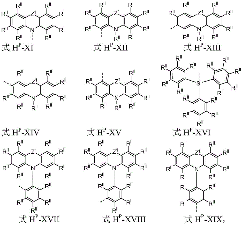
wherein, is present in p host material H P Each of the one or more second chemical moieties of (a) is attached to the first chemical moiety via a single bond represented by a dashed line in the above formula;
wherein,,
Z 1 independently at each occurrence selected from the group consisting of direct bond, C (R) II ) 2 、C=C(R II ) 2 、C=O、C=NR II 、NR II 、O、Si(R II ) 2 S, S (O) and S (O) 2 A group of;
R I each occurrence is independently of the other a binding site for a single bond connecting the first chemical moiety to the second chemical moiety, or is selected from the group consisting of: hydrogen; deuterium; me; i Pr; and t bu; and Ph optionally substituted with one or more substituents independently of each other selected from the group consisting of: me; i Pr; t bu; and Ph;
wherein at least one R I Is the binding site for a single bond linking a first chemical moiety to a second chemical moiety;
R II independently of each other at each occurrence selected from the group consisting of: hydrogen; deuterium; me; i Pr; t bu; and Ph optionally substituted with one or more substituents independently of each other selected from the group consisting of: me; i Pr; t bu; and Ph;
wherein two or more adjacent substituents R II A monocyclic or polycyclic aliphatic or aromatic or heteroaromatic carbocyclic or heterocyclic ring system may optionally be formed such that a ring is formed according to formula H P -XI, formula H P -XII, formula H P -XIII, formula H P -XIV, formula H P -XV, H P -XVI, H P -XVII, formula H P -XVIII and formula H P -structure of any of XIX and optionally substituted with adjacent substituents R II The fused ring system of the additional ring formed comprises a total of 8 to 60 carbon atoms, preferably 12 to 40 carbon atoms, more preferably 14 to 32 carbon atoms.
In an even more preferred embodiment of the invention, Z 1 At each occurrence is a direct bond, and adjacent substituents R II Does not bindTo form an additional ring system.
In an even more preferred embodiment of the invention, a p-body H optionally comprised in an organic electroluminescent device according to the invention P Selected from the group consisting of:


in a preferred embodiment of the invention, n-host H is optionally included in any of the one or more light emitting layers B as a whole (made up of or comprising more than one (sub) layer) N Including according to H N -I, formula H N -II and formula H N -structure of any one of III, or of formula H N -I, formula H N -II and formula H N -structural composition of any one of III:

wherein R is III And R is IV Independently of each other at each occurrence selected from the group consisting of: hydrogen; deuterium; me; i Pr; t Bu;CN;CF 3 the method comprises the steps of carrying out a first treatment on the surface of the Ph, optionally substituted with one or more substituents independently of each other selected from the group consisting of: me; i Pr; t bu; and Ph; from H N -IV, formula H N V, H N -VI, formula H N -VII, formula H N -VIII, formula H N -IX, H N -X, H N -XI, formula H N -XII, formula H N -XIII and formula H N -structure represented by any one of XIV:
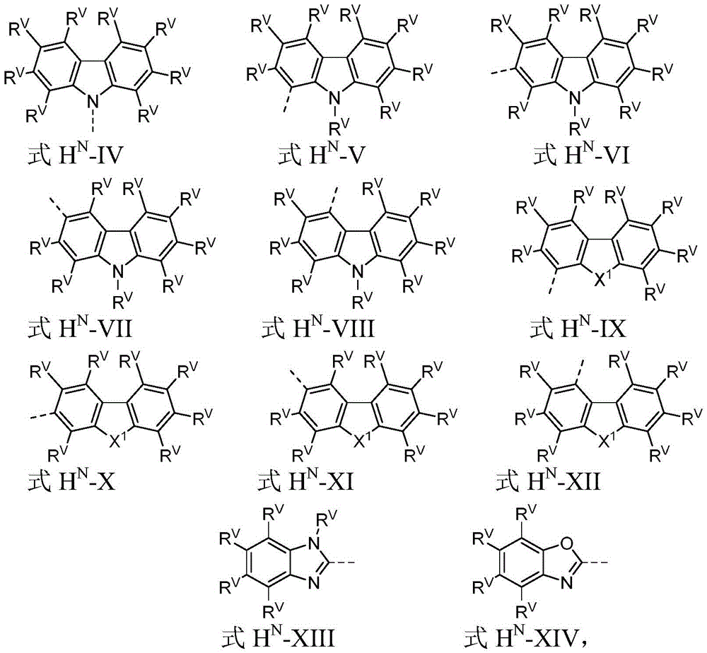
wherein,,
the dotted line indicates that the formula H will be followed N -IV, formula H N V, H N -VI, formula H N -VII, formula H N -VIII, formula H N -IX, H N -X, H N -XI, formula H N -XII, formula H N -XIII and formula H N The structure of any of XIVs is connected to a structure according to formula H N -I, formula H N -II and formula H N -a binding site for a single bond of the structure of any one of III;
X 1 is oxygen (O), sulfur (S) or C (R) V ) 2 ;
R V Independently of each other at each occurrence selected from the group consisting of: hydrogen; deuterium; me; i Pr; t bu; and Ph optionally substituted with one or more substituents independently of each other selected from the group consisting of: me; i Pr; t bu; and Ph;
wherein two or more adjacent substituents R V A monocyclic or polycyclic aliphatic or aromatic or heteroaromatic carbocyclic or heterocyclic ring system may optionally be formed such that a ring is formed according to formula H N -IV, formula H N V, H N -VI, formula H N -VII, formula H N -VIII, formula H N -IX, H N -X, H N -XI, formula H N -XII, formula H N -XIII and formula H N -structure of any one of XIV, optionally by adjacent substituents R V The fused ring system of the additional ring formed comprises a total of 8 to 60 carbon atoms, preferably 12 to 40 carbon atoms, more preferably 14 to 32 carbon atoms; and is also provided with
Wherein in formula H N -I and formula H N In formula II, at least one substituent R III Is CN.
Even more preferred in the inventionN-body H optionally included in an organic electroluminescent device according to the invention N Selected from the group consisting of:


in one embodiment of the invention, an n-host H included in any of the light emitting layers B of the organic electroluminescent device according to the invention N Does not contain any phosphine oxide groups, and in particular, n host H N Not bis [2- (diphenylphosphino) phenyl ]]Ether oxide (DPEPO).
Excitation energy transfer component EET-2
For the light-emitting layer B, TADF material E is preferably selected B And optional excitation energy transfer components EET-2, such that they are capable of transferring excitation energy to a small FWHM emitter S comprised in the same light emitting layer B of the organic electroluminescent device according to the invention B 。
In order to achieve this energy transfer, it is preferred that in TADF material E B Emission spectra (e.g., fluorescence spectra) and E at room temperature (i.e., (approximately) 20 ℃) B Small FWHM emitter S to which energy should be transferred B There is a spectral overlap between the absorption spectra at room temperature (i.e., (approximately) 20 ℃). Thus, in a preferred embodiment, within the light emitting layer B, within the TADF material E B Emission spectrum at room temperature (i.e., (approximately) 20 ℃) with a small FWHM emitter S B There is a spectral overlap between the absorption spectra at room temperature (i.e., (approximately) 20 ℃). Absorption and emission spectra are as described in the subsections that follow herein.
In a preferred embodiment of the invention, an optional excitation energy transfer component EET-2 transfers excitation energy to a small FWHM emitter S within the luminescent layer B B 。
To achieve such energy conversionPreferably, the emission spectrum of EET-2 at room temperature (i.e., (approximately) 20 ℃) is shifted (e.g., if EET-2 is TADF material E) B Fluorescence spectrum and if EET-2 is phosphorescent material P B Then phosphorescence spectrum, see below) and small FWHM emitter S to which EET-2 should transfer energy B There is a spectral overlap between the absorption spectra at room temperature (i.e., (approximately) 20 ℃). Thus, in a preferred embodiment, within the luminescent layer B, the emission spectrum at room temperature (i.e., (approximately) 20 ℃) with the small FWHM emitter S at the optional excitation energy transfer component EET-2 B There is a spectral overlap between the absorption spectra at room temperature (i.e., (approximately) 20 ℃). Absorption and emission spectra are as described in the subsections that follow herein.
In an even more preferred embodiment of the invention, within the light emitting layer B, a TADF material E is included in the light emitting layer B B An optional excitation energy transfer component EET-2 transfers energy to a small FWHM emitter S B 。
In a preferred embodiment of the invention, within the light emitting layer B, both of the following two conditions are satisfied:
(i) In TADF Material E B Emission spectrum at room temperature (i.e., (approximately) 20 ℃) with a small FWHM emitter S B There is a spectral overlap between the absorption spectra at room temperature (i.e., (approximately) 20 ℃); and is also provided with
(ii) Emission spectrum at room temperature (i.e., (approximately) 20 ℃) with small FWHM emitter S at optional excitation energy transfer component EET-2 B There is a spectral overlap between the absorption spectra at room temperature (i.e., (approximately) 20 ℃);
wherein the absorption spectrum and the emission spectrum are recorded as described in the subsections later herein.
In a preferred embodiment, within the light emitting layer B, TADF material E B Is the lowest unoccupied molecular orbital LUMO (E) B ) Having an energy E of less than-2.3 eV LUMO (E B ):E LUMO (E B )<-2.3eV。
In a preferred embodiment, within the light emitting layer B, TADF material E B The lowest unoccupied molecule of (2)Orbit LUMO (E) B ) Having an energy E of less than-2.6 eV LUMO (E B ):E LUMO (E B )<-2.6eV。
In a preferred embodiment, within the light emitting layer B, TADF material E B Highest occupied molecular orbital HOMO (E) B ) Having an energy E higher than-6.3 eV HOMO (E B ):E HOMO (E B )>-6.3eV。
In a preferred embodiment, within the light emitting layer B, the following two conditions are satisfied:
(i) TADF Material E B Is the lowest unoccupied molecular orbital LUMO (E) B ) Having an energy E of less than-2.6 eV LUMO (E B ):E LUMO (E B )<-2.6eV; and is also provided with
(ii) TADF Material E B Highest occupied molecular orbital HOMO (E) B ) Having an energy E higher than-6.3 eV HOMO (E B ):E HOMO (E B )>-6.3eV。
In one embodiment of the invention, within the light emitting layer B, the optional excitation energy transfer component EET-2 fulfils at least one (preferably exactly one) of the following two conditions:
(i) Which exhibits a delta E of less than 0.4eV (preferably less than 0.3eV, more preferably less than 0.2eV, even more preferably less than 0.1eV, or even less than 0.05 eV) ST Value, deltaE ST The value corresponds to E (S1 EET-2 ) And E (T1) EET-2 ) Energy difference between them; and/or
(ii) It comprises at least one (preferably exactly one) transition metal having a standard atomic weight of more than 40 (meaning that at least one atom within EET-2 is a (transition) metal having an atomic weight of more than 40, wherein the transition metal may be in any oxidation state).
In a preferred embodiment, within the light emitting layer B, TADF material E B Exhibit a ΔE of less than 0.4eV, preferably less than 0.3eV, more preferably less than 0.2eV, even more preferably less than 0.1eV or even less than 0.05eV ST Value, deltaE ST The value corresponds to the lowest excited singlet energy level E (S1 E ) And the lowest excited triplet level E (T1) E ) Energy difference between them.
In a preferred embodiment, within the light emitting layer B, the optional excitation energy transfer component EET-2 comprises at least one (preferably exactly one) transition metal having a standard atomic weight of more than 40 (meaning that EET-2 is a (transition) metal having an atomic weight of more than 40, wherein the transition metal may be in any oxidation state).
In a preferred embodiment of the invention, within each light emitting layer B, both of the following two conditions are satisfied:
(i) TADF Material E B Exhibit a ΔE of less than 0.4eV (preferably less than 0.3eV, more preferably less than 0.2eV, even more preferably less than 0.1eV, or even less than 0.05 eV) ST Value, deltaE ST The value corresponds to the lowest excited singlet energy level E (S1 E ) And the lowest excited triplet level E (T1) E ) Energy difference between them; and is also provided with
(ii) The optional excitation energy transfer component EET-2 comprises at least one (preferably exactly one) transition metal having a standard atomic weight of greater than 40 (meaning that at least one atom within the corresponding EET-2 is a (transition) metal having an atomic weight of greater than 40, wherein the transition metal may be in any oxidation state).
In a preferred embodiment of the invention, in the light-emitting layer B, the optional excitation energy transfer component EET-2 fulfils at least one (preferably exactly one) of the following two conditions:
(i) It exhibits a ΔE of less than 0.4eV, preferably less than 0.3eV, more preferably less than 0.2eV, even more preferably less than 0.1eV, or even less than 0.05eV (see below)) ST Value, deltaE ST The value corresponds to the lowest excited singlet energy level E (S1 EET-2 ) And the lowest excited triplet level E (T1) EET-2 ) Energy difference between them; and/or
(ii) It comprises iridium (Ir), palladium (Pd) or platinum (Pt) (meaning that at least one atom within EET-2 is iridium (Ir), palladium (Pd) or platinum (Pt), wherein Ir, pd and Pt may be in any oxidation state, see below).
In a preferred embodiment, within at least one (preferably each) light emitting layer B, at least one (preferably each) optional excitation energy transfer component EET-2 comprises iridium (Ir) or platinum (Pt) (meaning that at least one atom within the respective EET-2 is iridium (Ir) or platinum (Pt), wherein Ir and Pt may be in any oxidation state, see below).
As previously mentioned, in the context of the present invention, the light emitting layer B comprises TADF material E B And an optional excitation energy transfer component EET-2, wherein the two substances are not identical (i.e., they do not have the same chemical formula). This means that, in each light-emitting layer B of the organic electroluminescent device according to the invention, TADF material E B And the excitation energy transfer component EET-2 may be selected, for example, independently of one another, from the TADF material E B The chemical structures of the groups may be different in any case. That is, in the light-emitting layer B, there is no E B Has the same chemical formula (or structure) as EET-2.
In a particularly preferred embodiment, the optional excitation energy transfer component EET-2 optionally comprised in the organic electroluminescent device according to the invention is a phosphorescent material P as defined herein B 。
In a particularly preferred embodiment, the optional excitation energy transfer component EET-2 optionally comprised in the organic electroluminescent device according to the invention may be of a TADF material E as defined herein B TADF material of defined structural characteristics.
It is understood that if the excitation energy transfer component is selected as the TADF material, then the following is directed to TADF material E B Any of the preferred features, properties and embodiments described may also be applied to the optional excitation energy transfer component EET-2.
It is also understood that if the excitation energy transfer component is selected as the phosphorescent material P B Then hereinafter for phosphorescent material P B Any of the preferred features, properties and embodiments described may also be applied to the optional excitation energy transfer component EET-2.
TADF material(s) E B
As known to those skilled in the art, light emission from an emitter material (i.e., an emissive dopant) in, for example, an Organic Light Emitting Diode (OLED) may include fluorescence from an excited singlet state (typically the lowest excited singlet state S1) and phosphorescence from an excited triplet state (typically the lowest excited triplet state T1).
In the context of the present invention, a fluorescent emitter is capable of emitting light at room temperature (i.e., (approximately) 20 ℃) upon electron excitation (e.g., in an organic electroluminescent device), wherein the emitted excited state is a singlet state (typically the lowest excited singlet state S1). Fluorescent emitters typically exhibit instant (i.e., direct) fluorescence on a nanosecond time scale when initial electron excitation (e.g., by electron-hole recombination) provides an excited singlet state of the emitter.
In the context of the present invention, a delayed fluorescent material is a material capable of reaching an excited triplet state (typically from the lowest excited triplet state T1) from an excited triplet state (typically from the lowest excited triplet state S1) by means of reverse intersystem crossing (RISC), in other words: upward intersystem crossing or reverse intersystem crossing), and also capable of emitting light upon returning from the excited triplet state thus reached (typically S1) to its electronic ground state. Fluorescence emission observed from the excited triplet state (typically T1) to the emission excited singlet state (typically S1) after RISC occurs on a time scale (typically in the range of microseconds) that is slower than the time scale (typically in the range of nanoseconds) at which direct (i.e., instant) fluorescence occurs, and is therefore referred to as Delayed Fluorescence (DF). When RISC from an excited triplet state (typically from T1) to an excited singlet state (typically to S1) occurs by thermal activation, and if the excited singlet state thus filled emits light (delayed fluorescence emission), this process is called Thermally Activated Delayed Fluorescence (TADF). Thus, as described above, a TADF material is a material capable of emitting Thermally Activated Delayed Fluorescence (TADF). As is known to those skilled in the art, when the energy difference ΔE between the lowest excited singlet energy level E (S1) and the lowest excited triplet energy level E (T1) of the fluorescent emitter ST When reduced, a population of the lowest excited triplet states can be generated from the lowest excited triplet states with high efficiency by means of RISC. Thus, TADF materials will typically have a small Δe ST Values (see below), which form part of the common general knowledge of a person skilled in the art.
The occurrence of (thermally activated) delayed fluorescence may be analyzed, for example, based on decay curves obtained from time-resolved (i.e., transient) Photoluminescence (PL) measurements. PL emission from TADF materials is separated into an emission component from an excited singlet state (typically S1) generated by initial excitation and an emission component from an excited singlet state (typically S1) generated by RISC via an excited triplet state (typically T1). There is typically a significant time difference between emission from the excited singlet state (typically S1) formed by the initial excitation and emission from the excited singlet state (typically S1) arriving from the excited triplet state (typically T1) via RISC.
The TADF material preferably satisfies the following two conditions with respect to the kinetics of total attenuation:
(i) Decay kinetics exhibit two time regions, one typically in the nanosecond (ns) range and the other typically in the microsecond (μs) range; and
(ii) The shape of the emission spectrum in the two time zones is consistent;
Wherein part of the light emitted in the first attenuation zone is regarded as instant fluorescence and part of the light emitted in the second attenuation zone is regarded as delayed fluorescence. PL measurements can be performed using the corresponding emitter (i.e., the hypothetical TADF material) with a spin-coating film of 1 wt.% to 10 wt.% (specifically, 10 wt.%) of the corresponding emitter in poly (methyl methacrylate) (PMMA).
To evaluate whether the preferred criterion (i) is met (i.e., the decay kinetics exhibit two time zones, one typically in the nanosecond (ns) range and the other typically in the microsecond (μs) range), TCSPC (time dependent single photon counting) can typically be used (see below), and the full decay kinetics can typically be analyzed as follows. Alternatively, transient photoluminescence measurements with spectral resolution may be performed (see below).
To evaluate whether the preferred criterion (ii) is met (i.e. the shape of the emission spectra in the two time zones is consistent), transient photoluminescence measurements with spectral resolution may typically be performed (see below).
Experimental details for these measurements are provided in the subsections later herein.
The ratio of delayed fluorescence to instant fluorescence (n value) can be calculated by integration over time of the corresponding photoluminescence decay as shown in the subsection herein after.
In the context of the present invention, TADF materials preferably exhibit n values (ratio of delayed fluorescence to instant fluorescence) of greater than 0.05 (n > 0.05) (more preferably greater than 0.15 (n > 0.15), more preferably greater than 0.25 (n > 0.25), more preferably greater than 0.35 (n > 0.35), more preferably greater than 0.45 (n > 0.45), more preferably greater than 0.55 (n > 0.55), more preferably greater than 0.65 (n > 0.65), more preferably greater than 0.75 (n > 0.75), more preferably greater than 0.85 (n > 0.85), or even greater than 0.95 (n > 0.95)).
According to the invention, a Thermally Activated Delayed Fluorescence (TADF) material E B Characterized by exhibiting a delta E of less than 0.4eV, preferably less than 0.3eV, more preferably less than 0.2eV, even more preferably less than 0.1eV or even less than 0.05eV ST Value, deltaE ST The value corresponds to the lowest excited singlet energy level E (S1 E ) And the lowest excited triplet level E (T1) E ) Energy difference between them. Thus, TADF Material E according to the invention B Delta E of (2) ST Can be small enough to allow the lowest excited singlet S1 at room temperature (RT, i.e., (approximately) 20 ℃) E From the lowest excited triplet state T1 E Thermal refill (thermal repopulation) (also referred to as upward intersystem crossing or reverse intersystem crossing, RISC).
Preferably, in the context of the present invention, TADF material E B Shows both instant fluorescence and delayed fluorescence (when RISC is activated from T1 via heat) E State of reaching emission S1 E State time) of the two.
It is understood that the small FWHM emitter S included in the light emitting layer B of the organic electroluminescent device according to the present invention B May also optionally have a ΔE of less than 0.4eV ST Values, and exhibits Thermally Activated Delayed Fluorescence (TADF). However, for any small FWHM emitter S in the context of the invention B This is only an optional feature.
Hair-on-hairIn a preferred embodiment, in at least one TADF material E B And at least one small FWHM emitter S B There is a spectral overlap between the absorption spectra (when both spectra are measured under comparable conditions). In this case, TADF Material E B The energy can be transferred to at least one small FWHM emitter S B 。
According to the invention, TADF Material E B Having an emission maximum in the deep blue wavelength range of 380nm to 470nm (preferably 400nm to 470 nm) typically by employing 10 wt.% of TADF material E in poly (methyl methacrylate) PMMA at room temperature (i.e., (approximately) 20 ℃) B Is measured by spin-coating film.
In a preferred embodiment of the invention, in the context of the present invention, TADF material E B Emission maximum (peak emission) at a smaller FWHM emitter S B At a wavelength short of the emission maximum (peak emission).
In a preferred embodiment of the invention, each TADF material E B Is an organic TADF material, which in the context of the invention means that it does not contain any transition metal. Preferably, each TADF material E according to the invention B Mainly composed of the elements hydrogen (H), carbon (C) and nitrogen (N), but may also include, for example, oxygen (O), boron (B), silicon (Si), fluorine (F) and bromine (Br).
In a preferred embodiment of the invention, each TADF material E B Has a molecular weight of 800g/mol or less.
In one embodiment of the invention, TADF Material E B Exhibit a photoluminescence quantum yield (PLQY) equal to or higher than 30% by employing 10 wt% TADF material E in poly (methyl methacrylate) PMMA, typically at room temperature (i.e., (approximately) 20 ℃) B Is measured by spin-coating film.
In a preferred embodiment of the invention, the TADF emitter E B Exhibit a photoluminescence quantum yield (PLQY) equal to or higher than 50% by employing typically 10% by weight in poly (methyl methacrylate) PMMA at room temperature (i.e., (approximately) 20 ℃) TADF Material E B Is measured by spin-coating film.
In an even more preferred embodiment of the invention, the TADF emitter E B Exhibit a photoluminescence quantum yield (PLQY) equal to or higher than 70% by employing 10 wt% TADF material E in poly (methyl methacrylate) PMMA, typically at room temperature (i.e., (approximately) 20 ℃) B Is measured by spin-coating film.
In one embodiment of the invention, TADF Material E B :
(i) Characterized by exhibiting a delta E of less than 0.4eV ST Value of delta E ST The value corresponds to the lowest excited singlet energy level E (S1 E ) And the lowest excited triplet level E (T1) E ) Energy difference between them; and is also provided with
(ii) Shows a photoluminescence quantum yield (PLQY) of more than 30%.
In one embodiment of the invention, each TADF material E B Is the lowest unoccupied molecular orbital LUMO (E) B ) Energy E of (2) LUMO (E B ) Less than-2.6 eV.
It will be noted that although typically capable of emitting fluorescence and (thermally activated) delayed fluorescence, TADF material E included in the inventive organic electroluminescent device B Preferably primarily as an "energy pump" rather than as an emitter material. That is, the phosphorescent material P included in the light emitting layer B B Preferably primarily transfer excitation energy to one or more small FWHM emitters S B Small FWHM emitter S B Which in turn serves as the primary emitter material(s). Phosphorescent material P in light-emitting layer B B Preferably not emitting light. However, it may emit light to some extent.
Those skilled in the art know how to design a TADF material (molecule) E according to the invention B And the structural features that such molecules typically exhibit. Briefly, to facilitate reverse inter-line crossover (RISC), ΔE is typically reduced ST In the context of the present invention, ΔE, as described above ST Less than 0.4eV. This is typically accomplished by designing the TADF material E B Is realized such that HOMO and LUMOAre separated spatially in large numbers on the (electron) donor and (electron) acceptor groups, respectively. These groups are typically bulky or joined via a spiro union such that they twist and the spatial overlap of HOMO and LUMO is reduced. However, minimizing spatial overlap of HOMO and LUMO also results in a reduction of the photoluminescence quantum yield (PLQY) of the TADF material, which is disadvantageous. Thus, in practice, both effects are considered to achieve ΔE ST Is reduced and PLQY is high.
One common method for designing TADF materials is to covalently attach one or more (electron) donor moieties with HOMO distributed thereon and one or more (electron) acceptor moieties with LUMO distributed thereon to the same bridge, referred to herein as a linking group. TADF Material E B Two or three linking groups may be included, for example, that are bound to the same acceptor moiety, and additional donor and acceptor moieties may be bound to each of the two or three linking groups.
One or more donor moieties and one or more acceptor moieties may also be directly bound to each other (in the absence of a linking group).
Typical donor moieties are diphenylamines, carbazoles, acridines, phenoxazines and derivatives of related structures.
Benzene derivatives, biphenyl derivatives and to some extent also terphenyl derivatives are common linking groups.
Nitrile groups are very common acceptor moieties in TADF materials, known examples of which include:
(i) Carbazolyl dicyanobenzene compounds
Such as 2CzPN (4, 5-bis (9H-carbazol-9-yl) phthalonitrile), DCzIPN (4, 6-bis (9H-carbazol-9-yl) isophthalonitrile), 4CzPN (3, 4,5, 6-tetrakis (9H-carbazol-9-yl) phthalonitrile), 4CzIPN (2, 4,5, 6-tetrakis (9H-carbazol-9-yl) isophthalonitrile), 4CzTPN (2, 4,5, 6-tetrakis (9H-carbazol-9-yl) terephthalonitrile) and derivatives thereof;
(ii) Carbazolyl cyanopyridine compounds
Such as 4CzCNPy (2, 3,5, 6-tetrakis (9H-carbazol-9-yl) -4-cyanopyridine) and derivatives thereof;
(iii) Carbazolyl cyanobiphenyl compounds
Such as CNBPCz (4, 4', 5' -tetra (9H-carbazol-9-yl) - [1,1' -biphenyl ] -2,2' -dinitrile), czBPCN (4, 4', 6' -tetra (9H-carbazol-9-yl) - [1,1' -biphenyl ] -3,3' -dinitrile), DDCzIPN (3, 3', 5' -tetra (9H-carbazol-9-yl) - [1,1' -biphenyl ] -2,2', 6' -tetramethylnitrile) and derivatives thereof;
wherein, in these materials, one or more of the nitrile groups may be treated as acceptor moiety by fluorine (F) or trifluoromethyl (CF) 3 ) Instead of.
Nitrogen heterocycles such as triazine derivatives, pyrimidine derivatives, triazole derivatives, oxadiazole derivatives, thiadiazole derivatives, heptazine derivatives, 1, 4-diazabenzo [9,10] phenanthrene derivatives, benzothiazole derivatives, benzoxazole derivatives, quinoxaline derivatives and diazafluorene derivatives are also well known acceptor moieties for use in constructing TADF materials. Known examples of TADF materials including, for example, triazine receptors include PIC-TRZ (7, 7' - (6- ([ 1,1' -biphenyl ] -4-yl) -1,3, 5-triazine-2, 4-diyl) bis (5-phenyl-5, 7-indolino [2,3-b ] carbazole)), mBFCzTrz (5- (3- (4, 6-diphenyl-1, 3, 5-triazin-2-yl) phenyl) -5H-benzofuro [3,2-c ] carbazole) and DCzTrz (9, 9' - (5- (4, 6-diphenyl-1, 3, 5-triazin-2-yl) -1, 3-phenylene) bis (9H-carbazole)).
Another group of TADF materials includes diaryl ketones such as benzophenone or (heteroaryl) aryl ketones such as 4-benzoylpyridine, 9, 10-anthraquinone, 9H-xanthen-9-one and derivatives thereof as acceptor moieties to which the donor moiety (typically of carbazolyl substituents) is bound. Examples of such TADF materials include BPBCz (bis (4- (9 ' -phenyl-9H, 9' H- [3,3' -dicarbazol ] -9-yl) phenyl) methanone), mDCBP ((3, 5-bis (9H-carbazol-9-yl) phenyl) (pyridin-4-yl) methanone), AQ-DTBu-Cz (2, 6-bis (4- (3, 6-di-tert-butyl-9H-carbazol-9-yl) phenyl) anthracene-9, 10-dione) and MCz-XT (3- (1, 3,6, 8-tetramethyl-9H-carbazol-9-yl) -9H-xanthen-9-one), respectively.
Sulfoxides (specifically diphenyl sulfoxide) are also commonly used as acceptor moieties for constructing TADF materials, and known examples include 4-PC-DPS (9-phenyl-3- (4- (phenylsulfonyl) phenyl) -9H-carbazole), ditBu-DPS (9, 9' - (sulfonylbis (4, 1-phenylene)) bis (9H-carbazole)) and TXO-PhCz (2- (9-phenyl-9H-carbazol-3-yl) -9H-thioxanthen-9-one 10, 10-dioxide).
Illustratively, all of the above groups of TADF materials may provide for a suitable TADF material E according to the invention B Assuming that the particular material meets the above basic requirements, i.e., ΔE ST The value is less than 0.4eV.
Those skilled in the art will appreciate that not only the above structures, but also more materials may be suitable TADF materials E in the context of the present invention B . Those skilled in the art are familiar with the design principles of such molecules and also know how to design such molecules with a certain emission color (e.g. blue, green or red emission).
See, for example: H.Tanaka, K.Shizu, H.Nakanotani, C.Adachi, chemistry of Materials2013,25 (18), 3766, DOI:10.1021/cm402428a; J.Li, T.Nakagawa, J.MacDonald, Q.Zhang, H.Nomura, H.Miyazaki, C.Adachi, advanced Materials2013,25 (24), 3319, DOI:10.1002/adma.201300575; K.Nasu, T.Nakagawa, H.Nomura, C.—J.Lin, C.—H.Cheng, M.— R.Tseng, T.Yasudaad, C.Adachi, chemical Communications 2013,49 (88), 10385, DOI:10.1039/c3cc44179b; Q.Zhang, B.Li1, S.Huang, H.Nomura, H.Tanaka, C.Adachi, nature Photonics 2014,8 (4), 326, DOI:10.1038/nphoton.2014.12; B.Wex, B.R.Kaafarani, journal of Materials Chemistry C2017, 5,8622, DOI:10.1039/c7tc02156a; Y.Im, M.Kim, Y.J.Cho, J. -A.Seo, K.S.Yook, J.Y.Lee, chemistry of Materials 2017,29 (5), 1946, DOI:10.1021/acs. Chemnater.6b05324; t. T.Bui, F.Goubard, M.Ibrahim-Oliali, D.Gigmes, F.Dumur, beilstein Journal of Organic Chemistry 2018,14,282, DOI:10.3762/bjoc.14.18; liang, Z. -L.Tu, Y. -X.zheng, chemistry-A European Journal 2019,25 (22), 5623, DOI:10.1002/chem.201805952.
Furthermore, for example, US2015105564 (A1), US2015048338 (A1), US2015141642 (A1), US2014336379 (A1), US2014138670 (A1), US2012241732 (A1), EP3315581 (A1), EP3483156 (A1) and US2018053901 (A1) disclose TADF materials E which can be used in the organic electroluminescent device according to the invention B . It is to be understood that this does not imply that the invention is limited to inclusion of the TADF materials disclosed in the cited referencesAn organic electroluminescent device. It is also understood that any TADF material used in the prior art may also be a suitable TADF material E in the context of the present invention B 。
In one embodiment of the invention, each TADF material E B Comprises, independently of one another, a group selected from CN, CF 3 And optionally substituted 1,3, 5-triazinyl.
In one embodiment of the invention, each TADF material E B Comprising one or more chemical moieties selected independently of each other from the group consisting of CN and optionally substituted 1,3, 5-triazinyl.
In one embodiment of the invention, each TADF material E B Comprising one or more optionally substituted 1,3, 5-triazinyl groups.
In one embodiment of the invention, each TADF material E B Including one or more chemical moieties selected from amino, indolyl, carbazolyl and derivatives thereof (all of which may optionally be substituted) independently of each other, wherein these groups may be bound to the core structure of the corresponding TADF material via nitrogen (N) or via a carbon (C) atom, and wherein the substituents bound to these groups may form a mono-or polycyclic aliphatic or aromatic or heteroaromatic carbocyclic or heterocyclic ring system.
In a preferred embodiment of the invention, at least one (preferably each) TADF material E B Comprising the following steps:
one or more first chemical moieties, independently of each other, selected from amino, indolyl, carbazolyl and derivatives thereof (all of which may optionally be substituted), wherein these groups may be bound to the core structure of the corresponding TADF material via nitrogen (N) or via a carbon (C) atom, and wherein the substituents bound to these groups may form a mono-or polycyclic aliphatic or aromatic or heteroaromatic carbocyclic or heterocyclic ring system; and
one or more second chemical moieties selected independently from CN, CF 3 And optionally substituted 1,3, 5-triazinyl.
Hair-on-hairIn an even more preferred embodiment, at least one (preferably each) TADF material E B Comprising the following steps:
one or more first chemical moieties, independently of each other, selected from amino, indolyl, carbazolyl and derivatives thereof (all of which may optionally be substituted), wherein these groups may be bound to the core structure of the corresponding TADF material via nitrogen (N) or via a carbon (C) atom, and wherein the substituents bound to these groups may form a mono-or polycyclic aliphatic or aromatic or heteroaromatic carbocyclic or heterocyclic ring system; and
One or more second chemical moieties, independently of each other, are selected from the group consisting of CN and optionally substituted 1,3, 5-triazinyl.
In an even more preferred embodiment of the invention, at least one (preferably each) TADF material E B Comprising the following steps:
one or more first chemical moieties, independently of each other, selected from amino, indolyl, carbazolyl and derivatives thereof (all of which may optionally be substituted), wherein these groups may be bound to the core structure of the corresponding TADF material via nitrogen (N) or via a carbon (C) atom, and wherein the substituents bound to these groups may form a mono-or polycyclic aliphatic or aromatic or heteroaromatic carbocyclic or heterocyclic ring system; and
one or more optionally substituted 1,3, 5-triazinyl groups.
It is known to the person skilled in the art that the expression "derivative thereof" means that the corresponding parent structure may optionally be substituted or that any atom within the corresponding parent structure may be replaced by, for example, an atom of another element.
In one embodiment of the invention, each TADF material E B Comprising the following steps:
one or more first chemical moieties each comprising or consisting of a structure according to formula D-I:
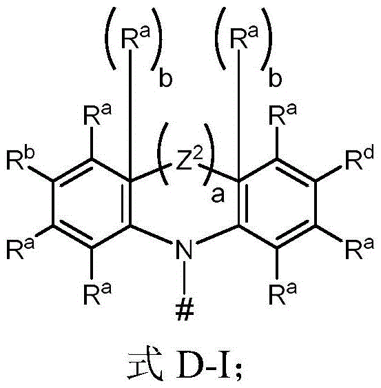
And
optionally, one or more second chemical moieties, each independently of the other, are selected from CN, CF 3 And a structure according to any one of formulas a-I, a-II, a-III, and a-IV:

and
A third chemical moiety comprising or consisting of a structure according to any of formulas L-I, L-II, L-III, L-IV, L-V, L-VI, L-VII, and L-VIII:

wherein,,
one or more first chemical moieties, optionally one or more second chemical moieties, are covalently bound to the third chemical moiety via a single bond;
wherein, in formula D-I:
# represents the binding site of a single bond connecting the corresponding first chemical moiety according to formula D-I to the third chemical moiety;
Z 2 independently at each occurrence selected from the group consisting of direct bond, CR 1 R 2 、C=CR 1 R 2 、C=O、C=NR 1 、NR 1 、O、SiR 1 R 2 S, S (O) and S (O) 2 A group of;
R a 、R b 、R d 、R 1 and R is 2 Independently of each other at each occurrence selected from the group consisting of: hydrogen; deuterium; n (R) 3 ) 2 ;OR 3 ;Si(R 3 ) 3 ;B(OR 3 ) 2 ;OSO 2 R 3 ;CF 3 ;CN;F;Cl;Br;I;C 1 -C 40 Alkyl optionally substituted with one or more substituents R 3 And wherein one or more non-adjacent CH' s 2 The radicals being optionally substituted by R 3 C=CR 3 、C≡C、Si(R 3 ) 2 、Ge(R 3 ) 2 、Sn(R 3 ) 2 、C=O、C=S、C=Se、C=NR 3 、P(=O)(R 3 )、SO、SO 2 、NR 3 O, S or CONR 3 Substitution; c (C) 1 -C 40 Alkoxy optionally substituted with one or more substituents R 3 And wherein one or more non-adjacent CH' s 2 The radicals being optionally substituted by R 3 C=CR 3 、C≡C、Si(R 3 ) 2 、Ge(R 3 ) 2 、Sn(R 3 ) 2 、C=O、C=S、C=Se、C=NR 3 、P(=O)(R 3 )、SO、SO 2 、NR 3 O, S or CONR 3 Substitution; c (C) 1 -C 40 Thioalkoxy optionally substituted with one or more substituents R 3 And wherein one or more non-adjacent CH' s 2 The radicals being optionally substituted by R 3 C=CR 3 、C≡C、Si(R 3 ) 2 、Ge(R 3 ) 2 、Sn(R 3 ) 2 、C=O、C=S、C=Se、C=NR 3 、P(=O)(R 3 )、SO、SO 2 、NR 3 O, S or CONR 3 Substitution; c (C) 2 -C 40 Alkenyl optionally substituted with one or more substituents R 3 And wherein one or more non-adjacent CH' s 2 The radicals being optionally substituted by R 3 C=CR 3 、C≡C、Si(R 3 ) 2 、Ge(R 3 ) 2 、Sn(R 3 ) 2 、C=O、C=S、C=Se、C=NR 3 、P(=O)(R 3 )、SO、SO 2 、NR 3 O, S or CONR 3 Substitution; c (C) 2 -C 40 Alkynyl, optionally substituted with one or more substituents R 3 And wherein one or more non-adjacent CH' s 2 The radicals being optionally substituted by R 3 C=CR 3 、Si(R 3 ) 2 、Ge(R 3 ) 2 、Sn(R 3 ) 2 、C=O、C=S、C=Se、C=NR 3 、P(=O)(R 3 )、SO、SO 2 、NR 3 O, S or CONR 3 Substitution; c (C) 6 -C 60 Aryl optionally substituted with one or more substituents R 3 The method comprises the steps of carrying out a first treatment on the surface of the C 3 -C 60 Heteroaryl, optionally substituted with one or more substituents R 3 ;
R 3 Independently of each other at each occurrence selected from the group consisting of: hydrogen; deuterium; n (R) 4 ) 2 ;OR 4 ;Si(R 4 ) 3 ;B(OR 4 ) 2 ;OSO 2 R 4 ;CF 3 ;CN;F;Br;I;C 1 -C 40 Alkyl optionally substituted with one or more substituents R 4 And wherein one or more non-adjacent CH' s 2 The radicals being optionally substituted by R 4 C=CR 4 、C≡C、Si(R 4 ) 2 、Ge(R 4 ) 2 、Sn(R 4 ) 2 、C=O、C=S、C=Se、C=NR 4 、P(=O)(R 4 )、SO、SO 2 、NR 4 O, S or CONR 4 Substitution; c (C) 1 -C 40 Alkoxy optionally substituted with one or more substituents R 4 And wherein one or more non-adjacent CH' s 2 The radicals being optionally substituted by R 4 C=CR 4 、C≡C、Si(R 4 ) 2 、Ge(R 4 ) 2 、Sn(R 4 ) 2 、C=O、C=S、C=Se、C=NR 4 、P(=O)(R 4 )、SO、SO 2 、NR 4 O, S or CONR 4 Substitution; c (C) 1 -C 40 Thioalkoxy optionally substituted with one or more substituents R 4 And wherein one or more non-adjacent CH' s 2 The radicals being optionally substituted by R 4 C=CR 4 、C≡C、Si(R 4 ) 2 、Ge(R 4 ) 2 、Sn(R 4 ) 2 、C=O、C=S、C=Se、C=NR 4 、P(=O)(R 4 )、SO、SO 2 、NR 4 O, S or CONR 4 Substitution; c (C) 2 -C 40 Alkenyl optionally substituted with one or more substituents R 4 And wherein one or more non-adjacent CH' s 2 The radicals being optionally substituted by R 4 C=CR 4 、C≡C、Si(R 4 ) 2 、Ge(R 4 ) 2 、Sn(R 4 ) 2 、C=O、C=S、C=Se、C=NR 4 、P(=O)(R 4 )、SO、SO 2 、NR 4 O, S or CONR 4 Substitution; c (C) 2 -C 40 Alkynyl, optionally substituted with one or more substituents R 4 And wherein one or more non-adjacent CH' s 2 The radicals being optionally substituted by R 4 C=CR 4 、Si(R 4 ) 2 、Ge(R 4 ) 2 、Sn(R 4 ) 2 、C=O、C=S、C=Se、C=NR 4 、P(=O)(R 4 )、SO、SO 2 、NR 4 O, S or CONR 4 Substitution; c (C) 6 -C 60 Aryl optionally substituted with one or more substituents R 4 The method comprises the steps of carrying out a first treatment on the surface of the C 3 -C 57 Heteroaryl, optionally substituted with one or more substituents R 4 ;
Wherein, optionally, any substituent R a 、R b 、R d 、R 1 、R 2 、R 3 And R is 4 Independently of each other and selected from R a 、R b 、R d 、R 1 、R 2 、R 3 And R is 4 Form a monocyclic or polycyclic, aliphatic or aromatic or heteroaromatic, carbocyclic or heterocyclic ring system;
R 4 each occurrence is selected from the group consisting of: hydrogen; deuterium; OPh; CF (compact flash) 3 ;CN;F;C 1 -C 5 Alkyl, wherein one or more hydrogen atoms are optionally replaced by deuterium, CN, CF independently of one another 3 Or F substitution; c (C) 1 -C 5 Alkoxy, wherein one or more hydrogen atoms are optionally replaced by deuterium, CN, CF independently of one another 3 Or F substitution; c (C) 1 -C 5 Thioalkoxy groups in which one or more hydrogen atoms are optionally replaced by deuterium, CN, CF independently of one another 3 Or F substitution; c (C) 2 -C 5 Alkenyl in which one or more hydrogen atoms are optionally replaced independently of one another by deuterium, CN, CF 3 Or F substitution; c (C) 2 -C 5 Alkynyl, wherein one or more hydrogen atoms are optionally replaced independently of each other by deuterium, CN, CF 3 Or F substitution; c (C) 6 -C 18 Aryl, wherein one or more hydrogen atoms are optionally replaced by deuterium, C 1 -C 5 Alkyl, ph or CN substitution; c (C) 3 -C 17 Heteroaryl, wherein one or more hydrogen atoms are optionally substituted independently of one another by deuterium, ph or C 1 -C 5 Alkyl substitution; n (C) 6 -C 18 Aryl group 2 ;N(C 3 -C 17 Heteroaryl group 2 The method comprises the steps of carrying out a first treatment on the surface of the N (C) 3 -C 17 Heteroaryl) (C) 6 -C 18 An aryl group);
a is an integer and is 0 or 1;
b is an integer and is at each occurrence 0 or 1, wherein two b are always the same;
wherein when the integer a is 1, the two integers b are 0, and when the two integers b are 1, the integer a is 0;
wherein in formulae A-I, A-II, A-III and A-IV:
the dotted line represents a single bond connecting the corresponding second chemical moiety according to formula a-I, formula a-II, formula a-III or formula a-IV to the third chemical moiety;
Q 1 Independently at each occurrence selected from nitrogen (N), CR 6 And CR (CR) 7 With the proviso that in formulae A-I, two adjacent radicals Q 1 Not both nitrogen (N); wherein, if the group Q in the formula A-I 1 Are not nitrogen (N), then the radicals Q 1 At least one of them is CR 7 ;
Q 2 Independently at each occurrence selected from nitrogen (N) and CR 6 With the proviso that in formulae A-II and A-III at least one group Q 2 Is nitrogen (N) and two adjacent radicals Q 2 Not both nitrogen (N);
R 6 and R is 8 Independently of each other at each occurrence selected from the group consisting of: hydrogen; deuterium; n (R) 9 ) 2 ;OR 9 ;Si(R 9 ) 3 ;B(OR 9 ) 2 ;OSO 2 R 9 ;CF 3 ;CN;F;Cl;Br;I;C 1 -C 40 Alkyl optionally substituted with one or more substituents R 9 And wherein one or more non-adjacent CH' s 2 The radicals being optionally substituted by R 9 C=CR 9 、C≡C、Si(R 9 ) 2 、Ge(R 9 ) 2 、Sn(R 9 ) 2 、C=O、C=S、C=Se、C=NR 9 、P(=O)(R 9 )、SO、SO 2 、NR 9 O, S or CONR 9 Substitution; c (C) 1 -C 40 Alkoxy optionally substituted with one or more substituents R 9 And wherein one or more non-adjacent CH' s 2 The radicals being optionally substituted by R 9 C=CR 9 、C≡C、Si(R 9 ) 2 、Ge(R 9 ) 2 、Sn(R 9 ) 2 、C=O、C=S、C=Se、C=NR 9 、P(=O)(R 9 )、SO、SO 2 、NR 9 O, S or CONR 9 Substitution; c (C) 1 -C 40 Thioalkoxy optionally substituted with one or more substituents R 9 And wherein one or more non-adjacent CH' s 2 The radicals being optionally substituted by R 9 C=CR 9 、C≡C、Si(R 9 ) 2 、Ge(R 9 ) 2 、Sn(R 9 ) 2 、C=O、C=S、C=Se、C=NR 9 、P(=O)(R 9 )、SO、SO 2 、NR 9 O, S or CONR 9 Substitution; c (C) 2 -C 40 Alkenyl optionally substituted with one or more substituents R 9 And wherein one or more non-adjacent CH' s 2 The radicals being optionally substituted by R 9 C=CR 9 、C≡C、Si(R 9 ) 2 、Ge(R 9 ) 2 、Sn(R 9 ) 2 、C=O、C=S、C=Se、C=NR 9 、P(=O)(R 9 )、SO、SO 2 、NR 9 O, S or CONR 9 Substitution; c (C) 2 -C 40 Alkynyl, optionally substituted with one or more substituents R 9 And wherein one or more non-adjacent CH' s 2 The radicals being optionally substituted by R 9 C=CR 9 、Si(R 9 ) 2 、Ge(R 9 ) 2 、Sn(R 9 ) 2 、C=O、C=S、C=Se、C=NR 9 、P(=O)(R 9 )、SO、SO 2 、NR 9 O, S or CONR 9 Substitution; c (C) 6 -C 60 Aryl optionally substituted with one or more substituents R 9 The method comprises the steps of carrying out a first treatment on the surface of the C 3 -C 60 Heteroaryl, optionally substituted with one or more substituents R 9 ;
R 9 Independently of each other at each occurrence selected from the group consisting of: hydrogen; deuterium; n (R) 10 ) 2 ;OR 10 ;Si(R 10 ) 3 ;B(OR 10 ) 2 ;OSO 2 R 10 ;CF 3 ;CN;F;Cl;Br;I;C 1 -C 40 Alkyl optionally substituted with one or more substituents R 10 And wherein one or more non-adjacent CH' s 2 The radicals being optionally substituted by R 10 C=CR 10 、C≡C、Si(R 10 ) 2 、Ge(R 10 ) 2 、Sn(R 10 ) 2 、C=O、C=S、C=Se、C=NR 10 、P(=O)(R 10 )、SO、SO 2 、NR 10 O, S or CONR 10 Substitution; c (C) 1 -C 40 Alkoxy optionally substituted with one or more substituents R 10 And wherein one or more non-adjacent CH' s 2 The radicals being optionally substituted by R 10 C=CR 10 、C≡C、Si(R 10 ) 2 、Ge(R 10 ) 2 、Sn(R 10 ) 2 、C=O、C=S、C=Se、C=NR 10 、P(=O)(R 10 )、SO、SO 2 、NR 10 O, S or CONR 10 Substitution; c (C) 1 -C 40 Thioalkoxy optionally substituted with one or more substituents R 10 And wherein one or more non-adjacent CH' s 2 The radicals being optionally substituted by R 10 C=CR 10 、C≡C、Si(R 10 ) 2 、Ge(R 10 ) 2 、Sn(R 10 ) 2 、C=O、C=S、C=Se、C=NR 10 、P(=O)(R 10 )、SO、SO 2 、NR 10 O, S or CONR 10 Substitution; c (C) 2 -C 40 Alkenyl optionally substituted with one or more substituents R 10 And wherein one or more non-adjacent CH' s 2 The radicals being optionally substituted by R 10 C=CR 10 、C≡C、Si(R 10 ) 2 、Ge(R 10 ) 2 、Sn(R 10 ) 2 、C=O、C=S、C=Se、C=NR 10 、P(=O)(R 10 )、SO、SO 2 、NR 10 O, S or CONR 10 Substitution; c (C) 2 -C 40 Alkynyl, optionally substituted with one or more substituents R 10 And wherein one or more non-adjacent CH' s 2 The radicals being optionally substituted by R 10 C=CR 10 、Si(R 10 ) 2 、Ge(R 10 ) 2 、Sn(R 10 ) 2 、C=O、C=S、C=Se、C=NR 10 、P(=O)(R 10 )、SO、SO 2 、NR 10 O, S or CONR 10 Substitution; c (C) 6 -C 60 Aryl optionally substituted with one or more substituents R 10 The method comprises the steps of carrying out a first treatment on the surface of the C 3 -C 60 Heteroaryl, optionally substituted with one or more substituents R 10 ;
R 10 Independently of each other at each occurrence selected from the group consisting of: hydrogen; deuterium; OPh; CF (compact flash) 3 ;CN;F;C 1 -C 5 Alkyl, wherein one or more hydrogen atoms are optionally replaced by deuterium, CN, CF independently of one another 3 Or F substitution; c (C) 1 -C 5 Alkoxy groups in which one or more hydrogen atoms are optionally substituted independently of one another by deuterium、CN、CF 3 Or F substitution; c (C) 1 -C 5 Thioalkoxy groups in which one or more hydrogen atoms are optionally replaced by deuterium, CN, CF independently of one another 3 Or F substitution; c (C) 2 -C 5 Alkenyl in which one or more hydrogen atoms are optionally replaced independently of one another by deuterium, CN, CF 3 Or F substitution; c (C) 2 -C 5 Alkynyl, wherein one or more hydrogen atoms are optionally replaced independently of each other by deuterium, CN, CF 3 Or F substitution; c (C) 6 -C 18 Aryl, wherein one or more hydrogen atoms are optionally replaced by deuterium, C 1 -C 5 Alkyl, ph or CN substitution; c (C) 3 -C 17 Heteroaryl, wherein one or more hydrogen atoms are optionally substituted independently of one another by deuterium, ph or C 1 -C 5 Alkyl substitution; n (C) 6 -C 18 Aryl group 2 ;N(C 3 -C 17 Heteroaryl group 2 The method comprises the steps of carrying out a first treatment on the surface of the N (C) 3 -C 17 Heteroaryl) (C) 6 -C 18 An aryl group);
R 7 independently at each occurrence selected from CN, CF 3 And a group consisting of structures according to formula EWG-I:

wherein R is X For example R 6 Defined and provided that at least one group R in the formula EWG-I X Is CN or CF 3 ;
Wherein two adjacent radicals R in the formulae A to IV 8 Optionally forming an aromatic ring fused to the structure of formula a-IV, wherein the optionally so formed fused ring system comprises a total of 9 to 18 ring atoms;
wherein in formula L-I, formula L-II, formula L-III, formula L-IV, formula L-V, formula L-VI, formula L-VII and formula L-VIII:
Q 3 independently at each occurrence selected from nitrogen (N) and CR 12 And provided that at least one Q 3 Is nitrogen (N);
R 11 each occurrence is independently of the other a binding site for a single bond connecting the first chemical moiety or the second chemical moiety to the third chemical moiety, or is independently of the other selected from the group consisting of: hydrogen; deuterium; f, performing the process; cl; br; i, a step of I; c (C) 1 -C 5 An alkyl group wherein one or more hydrogen atoms are optionally substituted with deuterium; c 6 -C 18 Aryl, wherein one or more hydrogen atoms are optionally replaced by deuterium, C 1 -C 5 Alkyl, C 6 -C 18 Aryl, F, cl, br, and I substitution;
R 12 for example R 6 As defined.
In a preferred embodiment of the present invention,
Z 2 independently at each occurrence selected from the group consisting of direct bond, CR 1 R 2 、C=CR 1 R 2 、C=O、C=NR 1 、NR 1 、O、SiR 1 R 2 S, S (O) and S (O) 2 A group of;
R a 、R b 、R d 、R 1 and R is 2 Independently of each other at each occurrence selected from the group consisting of: hydrogen; deuterium; n (R) 3 ) 2 ;OR 3 ;Si(R 3 ) 3 ;CF 3 ;CN;F;Cl;Br;I;C 1 -C 40 Alkyl optionally substituted with one or more substituents R 3 And wherein one or more non-adjacent CH' s 2 The radicals being optionally substituted by R 3 C=CR 3 、C≡C、Si(R 3 ) 2 、Ge(R 3 ) 2 、Sn(R 3 ) 2 、C=O、C=S、C=Se、C=NR 3 、P(=O)(R 3 )、SO、SO 2 、NR 3 O, S or CONR 3 Substitution; c (C) 6 -C 60 Aryl optionally substituted with one or more substituents R 3 The method comprises the steps of carrying out a first treatment on the surface of the C 3 -C 60 Heteroaryl, optionally substituted with one or more substituents R 3 ;
R 3 Independently of each other at each occurrence selected from the group consisting of: hydrogen; deuterium; n (R) 4 ) 2 ;OR 4 ;Si(R 4 ) 3 ;CF 3 ;CN;F;Br;I;C 1 -C 40 Alkyl optionally substituted with one or more substituents R 4 And wherein one or more non-adjacent CH' s 2 The radicals being optionally substituted by R 4 C=CR 4 、C≡C、Si(R 4 ) 2 、Ge(R 4 ) 2 、Sn(R 4 ) 2 、C=O、C=S、C=Se、C=NR 4 、P(=O)(R 4 )、SO、SO 2 、NR 4 O, S or CONR 4 Substitution; c (C) 6 -C 60 Aryl optionally substituted with one or more substituents R 4 The method comprises the steps of carrying out a first treatment on the surface of the C 3 -C 57 Heteroaryl, optionally substituted with one or more substituents R 4 ;
Wherein, optionally, the substituent R a 、R b 、R d 、R 1 、R 2 、R 3 And R is 4 Any one of which is independently selected from R a 、R b 、R d 、R 1 、R 2 、R 3 And R is 4 Form a monocyclic or polycyclic, aliphatic or aromatic or heteroaromatic, carbocyclic or heterocyclic ring system;
R 4 independently of each other at each occurrence selected from the group consisting of: hydrogen; deuterium; CF (compact flash) 3 ;CN;F;C 1 -C 5 Alkyl, wherein one or more hydrogen atoms are optionally replaced by deuterium, CN, CF independently of one another 3 Or F substitution; c (C) 6 -C 18 Aryl, wherein one or more hydrogen atoms are optionally replaced by deuterium, C 1 -C 5 Alkyl, ph or CN substitution; c (C) 3 -C 17 Heteroaryl, wherein one or more hydrogen atoms are optionally replaced by deuterium, C 1 -C 5 Alkyl groupOr Ph substitution; n (C) 6 -C 18 Aryl group 2 ;N(C 3 -C 17 Heteroaryl group 2 The method comprises the steps of carrying out a first treatment on the surface of the N (C) 3 -C 17 Heteroaryl) (C) 6 -C 18 An aryl group);
a is an integer and is 0 or 1;
b is an integer and is at each occurrence 0 or 1, wherein two b are always the same;
wherein when the integer a is 1, the two integers b are 0, and when the two integers b are 1, the integer a is 0;
Q 1 independently at each occurrence selected from nitrogen (N), CR 6 And CR (CR) 7 With the proviso that in formulae A-I, two adjacent radicals Q 1 Not both nitrogen (N); wherein, if the group Q in the formula A-I 1 Are not nitrogen (N), then the radicals Q 1 At least one of them is CR 7 ;
Q 2 Independently at each occurrence selected from nitrogen (N) and CR 6 With the proviso that in formulae A-II and A-III at least one group Q 2 Is nitrogen (N) and two adjacent radicals Q 2 Not both nitrogen (N);
R 6 and R is 8 Independently of each other at each occurrence selected from the group consisting of: hydrogen; deuterium; n (R) 9 ) 2 ;OR 9 ;Si(R 9 ) 3 ;CF 3 ;CN;F;Cl;Br;I;C 1 -C 40 Alkyl optionally substituted with one or more substituents R 9 And wherein one or more non-adjacent CH' s 2 The radicals being optionally substituted by R 9 C=CR 9 、C≡C、Si(R 9 ) 2 、Ge(R 9 ) 2 、Sn(R 9 ) 2 、C=O、C=S、C=Se、C=NR 9 、P(=O)(R 9 )、SO、SO 2 、NR 9 O, S or CONR 9 Substitution; c (C) 6 -C 60 Aryl optionally substituted with one or more substituents R 9 The method comprises the steps of carrying out a first treatment on the surface of the C 3 -C 60 Heteroaryl, optionally substituted with one or more substituents R 9 ;
R 9 Independently of each other at each occurrence selected from the group consisting of: hydrogen; deuterium; n (R) 10 ) 2 ;OR 10 ;Si(R 10 ) 3 ;CF 3 ;CN;F;Cl;Br;I;C 1 -C 40 Alkyl optionally substituted with one or more substituents R 10 And wherein one or more non-adjacent CH' s 2 The radicals being optionally substituted by R 10 C=CR 10 、C≡C、Si(R 10 ) 2 、Ge(R 10 ) 2 、Sn(R 10 ) 2 、C=O、C=S、C=Se、C=NR 10 、P(=O)(R 10 )、SO、SO 2 、NR 10 O, S or CONR 10 Substitution; c (C) 6 -C 60 Aryl optionally substituted with one or more substituents R 10 The method comprises the steps of carrying out a first treatment on the surface of the C 3 -C 60 Heteroaryl, optionally substituted with one or more substituents R 10 ;
R 10 Independently of each other at each occurrence selected from the group consisting of: hydrogen; deuterium; OPh; CF (compact flash) 3 ;CN;F;C 1 -C 5 Alkyl, wherein one or more hydrogen atoms are optionally replaced by deuterium, CN, CF independently of one another 3 Or F substitution; c (C) 6 -C 18 Aryl, wherein one or more hydrogen atoms are optionally replaced by deuterium, C 1 -C 5 Alkyl, ph or CN substitution; c (C) 3 -C 17 Heteroaryl, wherein one or more hydrogen atoms are optionally replaced by deuterium, C 1 -C 5 Alkyl or Ph substitution; n (C) 6 -C 18 Aryl group 2 ;N(C 3 -C 17 Heteroaryl group 2 The method comprises the steps of carrying out a first treatment on the surface of the N (C) 3 -C 17 Heteroaryl) (C) 6 -C 18 An aryl group);
R 7 independently at each occurrence selected from CN, CF 3 And a group consisting of structures according to formula EWG-I:

wherein R is X For example R 6 Defined, with the proviso that at least one group R X Is CN or CF 3 ;
Wherein two adjacent radicals R in the formulae A to IV 8 Optionally forming a structure fused to formulae A-IV and optionally substituted with one or more substituents R 10 An aromatic ring of (a); wherein the fused ring system optionally so formed comprises a total of 9 to 18 ring atoms;
Q 3 independently at each occurrence selected from nitrogen (N) and CR 12 And provided that at least one Q 3 Is nitrogen (N);
R 11 each occurrence is independently of the other a binding site for a single bond connecting the first chemical moiety or the second chemical moiety to the third chemical moiety, or is independently of the other selected from the group consisting of: hydrogen; deuterium; c (C) 1 -C 5 An alkyl group wherein one or more hydrogen atoms are optionally substituted with deuterium; c 6 -C 18 Aryl, wherein one or more hydrogen atoms are optionally replaced by deuterium, C 1 -C 5 Alkyl and C 6 -C 18 Aryl substitution;
R 12 for example R 6 Defined as follows;
wherein the maximum number of first and second chemical moieties attached to the third chemical moiety is only limited by the number of available binding sites on the third chemical moiety (in other words: substituent R 11 The number of (a) limits (under the above conditions, each TADF material E B Comprising at least one first chemical moiety, at least one second chemical moiety and exactly one third chemical moiety).
In an even more preferred embodiment of the invention,
Z 2 independently at each occurrence selected from the group consisting of direct bond, CR 1 R 2 、C=CR 1 R 2 、C=O、C=NR 1 、NR 1 、O、SiR 1 R 2 S, S (O) and S (O) 2 A group of;
R a 、R b 、R d 、R 1 and R is 2 Independently of each other at each occurrence selected from the group consisting of: hydrogen; deuterium; n (R) 3 ) 2 ;OR 3 ;Si(R 3 ) 3 ;CF 3 ;CN;F;Cl;Br;I;C 1 -C 5 Alkyl optionally substituted with one or more substituents R 3 ;C 6 -C 18 Aryl optionally substituted with one or more substituents R 3 The method comprises the steps of carrying out a first treatment on the surface of the C 3 -C 17 Heteroaryl, optionally substituted with one or more substituents R 3 ;
R 3 Independently of each other at each occurrence selected from the group consisting of: hydrogen; deuterium; n (R) 4 ) 2 ;Si(R 4 ) 3 ;CF 3 ;CN;F;C 1 -C 5 Alkyl optionally substituted with one or more substituents R 4 ;C 6 -C 18 Aryl optionally substituted with one or more substituents R 4 The method comprises the steps of carrying out a first treatment on the surface of the C 3 -C 17 Heteroaryl, optionally substituted with one or more substituents R 4 ;
Wherein, optionally, the substituent R a 、R b 、R d 、R 1 、R 2 And R is 3 Any one of which is independently selected from R a 、R b 、R d 、R 1 、R 2 And R is 3 Form a monocyclic or polycyclic, aliphatic or aromatic, carbocyclic or heterocyclic ring system; wherein the ring system thus formed may optionally be substituted with one or more substituents R 5 ;
R 4 And R is 5 Independently of each other at each occurrence selected from the group consisting of: hydrogen; deuterium; CF (compact flash) 3 ;CN;F;Me; i Pr; t Bu;N(Ph) 2 The method comprises the steps of carrying out a first treatment on the surface of the And Ph, wherein one or more hydrogen atoms are optionally substituted independently of each other by deuterium, me, i Pr、 t Bu and Ph substitutions;
a is an integer and is 0 or 1;
b is an integer and is at each occurrence 0 or 1, wherein two b are always the same;
wherein when the integer a is 1, the two integers b are 0, and when the two integers b are 1, the integer a is 0;
Q 1 independently at each occurrence selected from nitrogen (N), CR 6 And CR (CR) 7 With the proviso that in formulae A-I, two adjacent radicals Q 1 Not both nitrogen (N); wherein, if the group Q in the formula A-I 1 Are not nitrogen (N), then the radicals Q 1 At least one of them is CR 7 ;
Q 2 Independently at each occurrence selected from nitrogen (N) and CR 6 With the proviso that in formulae A-II and A-III at least one group Q 2 Is nitrogen (N) and two adjacent radicals Q 2 Not both nitrogen (N);
R 6 and R is 8 Independently of each other at each occurrence selected from the group consisting of: hydrogen; deuterium; n (R) 9 ) 2 ;OR 9 ;Si(R 9 ) 3 ;CF 3 ;CN;F;C 1 -C 5 Alkyl optionally substituted with one or more substituents R 9 ;C 6 -C 18 Aryl optionally substituted with one or more substituents R 9 The method comprises the steps of carrying out a first treatment on the surface of the C 3 -C 17 Heteroaryl, optionally substituted with one or more substituents R 9 ;
R 9 Independently of each other at each occurrence selected from the group consisting of: hydrogen; deuterium; n (R) 10 ) 2 ;OR 10 ;Si(R 10 ) 3 ;CF 3 ;CN;F;C 1 -C 5 Alkyl optionally substituted with one or more substituents R 10 ;C 6 -C 18 Aryl optionally substituted with one or more substituents R 10 The method comprises the steps of carrying out a first treatment on the surface of the C 3 -C 17 Heteroaryl, optionally substituted with one or more substituents R 10 ;
R 10 Independently at each occurrence selected fromIn the group consisting of: hydrogen; deuterium; me; i Pr; t Bu;CF 3 ;CN;F;N(Ph) 2 the method comprises the steps of carrying out a first treatment on the surface of the And Ph, wherein one or more hydrogen atoms are optionally substituted independently of each other by deuterium, me, i Pr、 t Bu、Ph、CN、CF 3 Or F substitution;
R 7 independently at each occurrence selected from CN, CF 3 And a group consisting of structures according to formula EWG-I:

wherein R is X For example R 6 Defined, with the proviso that at least one group R X Is CN or CF 3 ;
Wherein two adjacent radicals R in the formulae A to IV 8 Optionally forming an aromatic ring fused to the structure of formula a-IV, wherein the optionally so formed fused ring system comprises a total of 9 to 18 ring atoms;
Q 3 independently at each occurrence selected from nitrogen (N) and CR 12 And provided that at least one Q 3 Is nitrogen (N);
R 11 each occurrence is independently of the other a binding site for a single bond connecting the first chemical moiety or the second chemical moiety to the third chemical moiety, or is independently of the other selected from the group consisting of: hydrogen; deuterium; c (C) 1 -C 5 An alkyl group wherein one or more hydrogen atoms are optionally substituted with deuterium; c 6 -C 18 Aryl optionally substituted with one or more substituents independently selected from the group consisting of: deuterium; me; i Pr; t bu; and Ph;
R 12 for example R 6 As defined.
In an even more preferred embodiment of the invention,
Z 2 independently at each occurrence selected from the group consisting of direct bond, CR 1 R 2 、C=O、NR 1 、O、SiR 1 R 2 S, S (O) and S (O) 2 A group of;
R a 、R b 、R d 、R 1 and R is 2 Independently of each other at each occurrence selected from the group consisting of: hydrogen; deuterium; n (R) 3 ) 2 ;OR 3 ;Si(R 3 ) 3 ;CF 3 ;CN;C 1 -C 5 Alkyl optionally substituted with one or more substituents R 3 ;C 6 -C 18 Aryl optionally substituted with one or more substituents R 3 The method comprises the steps of carrying out a first treatment on the surface of the C 3 -C 17 Heteroaryl, optionally substituted with one or more substituents R 3 ;
R 3 Independently of each other at each occurrence selected from the group consisting of: hydrogen; deuterium; CF (compact flash) 3 ;CN;F;Me; i Pr; t Bu;N(Ph) 2 The method comprises the steps of carrying out a first treatment on the surface of the And Ph, wherein one or more hydrogen atoms are optionally substituted independently of each other by deuterium, me, i Pr、 t Bu and Ph substitutions;
wherein, optionally, the substituent R a 、R b 、R d 、R 1 And R is 2 Any one of which is independently selected from R a 、R b 、R d 、R 1 And R is 2 Wherein the optionally so formed fused ring system constructed from the structure according to formula D-I and the attached ring formed by the adjacent substituents together comprise in total 13 to 40 ring atoms, preferably 13 to 30 ring atoms, more preferably 16 to 30 ring atoms;
a is an integer and is 0 or 1;
b is an integer and is at each occurrence 0 or 1, wherein two b are always the same;
wherein when the integer a is 1, the two integers b are 0, and when the two integers b are 1, the integer a is 0;
Q 1 independently at each occurrence selected fromIn nitrogen (N), CR 6 And CR (CR) 7 With the proviso that in formulae A-I, two adjacent radicals Q 1 Not both nitrogen (N); wherein, if the group Q in the formula A-I 1 Are not nitrogen (N), then the radicals Q 1 At least one of them is CR 7 ;
Q 2 Independently at each occurrence selected from nitrogen (N) and CR 6 With the proviso that in formulae A-II and A-III at least one group Q 2 Is nitrogen (N) and two adjacent radicals Q 2 Not both nitrogen (N);
R 6 and R is 8 Independently of each other at each occurrence selected from the group consisting of: hydrogen; deuterium; n (R) 9 ) 2 ;OR 9 ;Si(R 9 ) 3 ;CF 3 ;CN;F;C 1 -C 5 Alkyl optionally substituted with one or more substituents R 9 ;C 6 -C 18 Aryl optionally substituted with one or more substituents R 9 The method comprises the steps of carrying out a first treatment on the surface of the C 3 -C 17 Heteroaryl, optionally substituted with one or more substituents R 9 ;
R 9 Independently of each other at each occurrence selected from the group consisting of: hydrogen; deuterium; me; i Pr; t Bu;CF 3 ;CN;F;N(Ph) 2 the method comprises the steps of carrying out a first treatment on the surface of the And Ph, wherein one or more hydrogen atoms are optionally substituted independently of each other by deuterium, me, i Pr、 t Bu、Ph、CN、CF 3 Or F substitution.
R 7 Independently at each occurrence selected from CN, CF 3 And a group consisting of structures according to formula EWG-I:


wherein R is X For example R 6 Defined, with the proviso that at least one group R X Is CN or CF 3 ;
Wherein two adjacent radicals R in the formulae A to IV 8 Optionally forming an aromatic ring fused to the structure of formula a-IV, wherein the optionally so formed fused ring system comprises a total of 9 to 18 ring atoms;
Q 3 Independently at each occurrence selected from nitrogen (N) and CR 12 And provided that at least one Q 3 Is nitrogen (N);
R 11 each occurrence is independently of the other a binding site for a single bond connecting the first chemical moiety or the second chemical moiety to the third chemical moiety, or is independently of the other selected from the group consisting of: hydrogen; deuterium; me; i Pr; t bu; and Ph optionally substituted with one or more substituents independently of each other selected from the group consisting of: deuterium; me; i Pr; t bu; and Ph;
R 12 for example R 6 As defined.
In an even more preferred embodiment of the invention,
Z 2 independently at each occurrence selected from the group consisting of direct bond, CR 1 R 2 、C=O、NR 1 、O、SiR 1 R 2 S, S (O) and S (O) 2 A group of;
R a 、R b and R is d Independently of each other at each occurrence selected from the group consisting of: hydrogen; deuterium; n (R) 3 ) 2 ;OR 3 ;Si(R 3 ) 3 ;CF 3 ;CN;Me; i Pr; t Bu; ph, wherein one or more hydrogen atoms are optionally replaced independently of each other by deuterium, me, i Pr、 t Bu and Ph substitutions; carbazolyl groups in which one or more hydrogen atoms are optionally substituted independently of one another by deuterium, me, i Pr、 t Bu and Ph substitutions; triazinyl groups in which one or more hydrogen atoms are optionally replaced independently of one another by deuterium, me, i Pr、 t Bu and Ph substitutions; pyrimidinyl radical, wherein One or more hydrogen atoms are optionally substituted independently of one another by deuterium, me, i Pr、 t Bu and Ph substitutions; and pyridyl, wherein one or more hydrogen atoms are optionally replaced by deuterium, me, i Pr、 t bu and Ph substitutions;
R 1 and R is 2 Independently of each other at each occurrence selected from the group consisting of: hydrogen; deuterium; n (R) 3 ) 2 ;OR 3 ;Si(R 3 ) 3 ;CF 3 ;CN;C 1 -C 5 Alkyl optionally substituted with one or more substituents R 3 ;C 6 -C 18 Aryl optionally substituted with one or more substituents R 3 The method comprises the steps of carrying out a first treatment on the surface of the C 3 -C 17 Heteroaryl, optionally substituted with one or more substituents R 3 ;
R 3 Independently of each other at each occurrence selected from the group consisting of: hydrogen; deuterium; CF (compact flash) 3 ;CN;F;Me; i Pr; t Bu; and Ph, wherein one or more hydrogen atoms are optionally substituted independently of each other by deuterium, me, i Pr、 t Bu and Ph substitutions;
wherein, optionally, the substituent R a 、R b 、R d 、R 1 And R is 2 Any one of which is independently selected from R a 、R b 、R d 、R 1 And R is 2 Wherein the optionally so formed fused ring system constructed from the structure according to formula D-I and the attached ring formed by the adjacent substituents together comprise in total 13 to 40 ring atoms, preferably 13 to 30 ring atoms, more preferably 16 to 30 ring atoms;
a is an integer and is 0 or 1;
b is an integer and is at each occurrence 0 or 1, wherein two b are always the same;
wherein when the integer a is 1, the two integers b are 0, and when the two integers b are 1, the integer a is 0;
Q 1 independently at each occurrence selected from nitrogen (N), CR 6 And CR (CR) 7 With the proviso that in formulae A-I, two adjacent radicals Q 1 Not both nitrogen (N); wherein, if the group Q in the formula A-I 1 Are not nitrogen (N), then the radicals Q 1 At least one of them is CR 7 ;
Q 2 Independently at each occurrence selected from nitrogen (N) and CR 6 With the proviso that in formulae A-II and A-III at least one group Q 2 Is nitrogen (N) and two adjacent radicals Q 2 Not both nitrogen (N);
R 6 and R is 8 Independently of each other at each occurrence selected from the group consisting of: hydrogen; deuterium; n (R) 9 ) 2 ;OR 9 ;Si(R 9 ) 3 ;CF 3 ;CN;F;C 1 -C 5 Alkyl optionally substituted with one or more substituents R 9 ;C 6 -C 18 Aryl optionally substituted with one or more substituents R 9 The method comprises the steps of carrying out a first treatment on the surface of the C 3 -C 17 Heteroaryl, optionally substituted with one or more substituents R 9 ;
R 9 Independently of each other at each occurrence selected from the group consisting of: hydrogen; deuterium; me; i Pr; t Bu;CF 3 ;CN;F;N(Ph) 2 the method comprises the steps of carrying out a first treatment on the surface of the And Ph, wherein one or more hydrogen atoms are optionally substituted independently of each other by deuterium, me, i Pr、 t Bu、Ph、CN、CF 3 Or F substitution;
R 7 independently at each occurrence selected from CN, CF 3 And a group consisting of structures according to formula EWG-I:

wherein R is X For example R 6 Defined, with the proviso that at least one group R X Is CN or CF 3 ;
Wherein two adjacent radicals R in the formulae A to IV 8 Optionally forming an aromatic ring fused to the structure of formula a-IV, wherein the optionally so formed fused ring system comprises a total of 9 to 18 ring atoms;
Q 3 independently at each occurrence selected from nitrogen (N) and CR 12 And provided that at least one Q 3 Is nitrogen (N);
R 11 each occurrence is independently of the other a binding site for a single bond connecting the first chemical moiety or the second chemical moiety to the third chemical moiety, or is independently of the other selected from the group consisting of: hydrogen; deuterium; me; i Pr; t bu; and Ph optionally substituted with one or more substituents independently of each other selected from the group consisting of: deuterium; me; i Pr; t bu; and Ph;
R 12 for example R 6 As defined.
In an even more preferred embodiment of the invention,
Z 2 independently at each occurrence selected from the group consisting of direct bond, CR 1 R 2 、C=O、NR 1 、O、SiR 1 R 2 S, S (O) and S (O) 2 A group of;
R a 、R b and R is d Independently of each other at each occurrence selected from the group consisting of: hydrogen; deuterium; n (R) 3 ) 2 ;OR 3 ;Si(R 3 ) 3 ;CF 3 ;CN;Me; i Pr; t Bu; ph, wherein one or more hydrogen atoms are optionally replaced independently of each other by deuterium, me, i Pr、 t Bu and Ph substitutions; and carbazolyl groups in which one or more hydrogen atoms are optionally substituted independently of one another by deuterium, me, i Pr、 t Bu and Ph substitutions;
R 1 and R is 2 Independently of each other at each occurrence selected from the group consisting of: hydrogen; deuterium; OR (OR) 3 ;Si(R 3 ) 3 ;C 1 -C 5 Alkyl, optionallySubstituted with one or more substituents R 3 The method comprises the steps of carrying out a first treatment on the surface of the C 6 -C 18 Aryl optionally substituted with one or more substituents R 3 The method comprises the steps of carrying out a first treatment on the surface of the And is also provided with
R 3 Independently of each other at each occurrence selected from the group consisting of: hydrogen; deuterium; CF (compact flash) 3 ;CN;F;Me; i Pr; t Bu; and Ph, wherein one or more hydrogen atoms are optionally substituted independently of each other by deuterium, me, i Pr、 t Bu and Ph substitutions;
wherein, optionally, the substituent R a 、R b 、R d 、R 1 And R is 2 Any one of which is independently selected from R a 、R b 、R d 、R 1 And R is 2 Wherein the optionally so formed fused ring system constructed from the structure according to formula D-I and the attached ring formed by adjacent substituents comprises in total 13 to 40 ring atoms, preferably 13 to 30 ring atoms, more preferably 16 to 30 ring atoms;
a is an integer and is 0 or 1;
b is an integer and is at each occurrence 0 or 1, wherein two b are always the same;
wherein when the integer a is 1, the two integers b are 0, and when the two integers b are 1, the integer a is 0;
Q 1 independently at each occurrence selected from nitrogen (N), CR 6 And CR (CR) 7 With the proviso that in formulae A-I, two adjacent radicals Q 1 Not both nitrogen (N); wherein, if the group Q in the formula A-I 1 Are not nitrogen (N), then the radicals Q 1 At least one of them is CR 7 ;
Q 2 Independently at each occurrence selected from nitrogen (N) and CR 6 With the proviso that in formulae A-II and A-III at least one group Q 2 Is nitrogen (N) and two adjacent radicals Q 2 Not both nitrogen (N);
R 6 and R is 8 Independently of each other at each occurrence selected from the group consisting of: hydrogen; deuterium; OPh; n (Ph) 2 ;Si(Me) 3 ;Si(Ph) 3 ;CF 3 ;CN;F;Me; i Pr; t Bu; ph, wherein one or more hydrogen atoms are optionally replaced independently of each other by deuterium, me, i Pr、 t Bu and Ph substitutions; and carbazolyl groups in which one or more hydrogen atoms are optionally substituted independently of one another by deuterium, me, i Pr、 t Bu and Ph substitutions;
R 7 independently at each occurrence selected from CN, CF 3 And a group consisting of structures according to formula EWG-I:
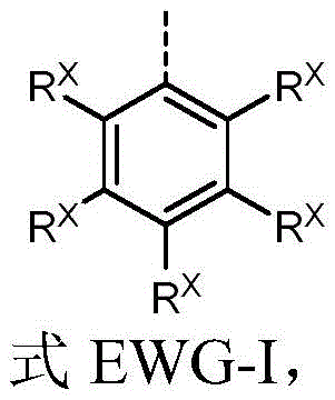
wherein R is X For example R 6 Defined, with the proviso that at least one group R X Is CN or CF 3 ;
Wherein two adjacent radicals R in the formulae A to IV 8 Optionally forming an aromatic ring fused to the structure of formula a-IV, wherein the optionally so formed fused ring system comprises a total of 9 to 18 ring atoms;
Q 3 independently at each occurrence selected from nitrogen (N) and CR 12 And provided that at least one Q 3 Is nitrogen (N);
R 11 each occurrence is independently of the other a binding site for a single bond connecting the first chemical moiety or the second chemical moiety to the third chemical moiety, or is independently of the other selected from the group consisting of: hydrogen; deuterium; me; i Pr; t bu; and Ph optionally substituted with one or more substituents independently of each other selected from the group consisting of: deuterium; me; i Pr; t bu; and Ph;
R 12 for example R 6 As defined.
In an even more preferred embodiment of the invention,
Z 2 independently at each occurrence selected from the group consisting of direct bond, CR 1 R 2 、C=O、NR 1 、O、SiR 1 R 2 S, S (O) and S (O) 2 A group of;
R a 、R b and R is d Independently of each other at each occurrence selected from the group consisting of: hydrogen; deuterium; n (Ph) 2 ;Si(Me) 3 ;Si(Ph) 3 ;CF 3 ;CN;Me; i Pr; t Bu; ph, wherein one or more hydrogen atoms are optionally replaced independently of each other by deuterium, me, i Pr、 t Bu and Ph substitutions; and carbazolyl groups in which one or more hydrogen atoms are optionally substituted independently of one another by deuterium, me, i Pr、 t Bu and Ph substitutions;
R 1 and R is 2 Independently of each other at each occurrence selected from the group consisting of: hydrogen; deuterium; me; i Pr; t bu; and Ph, wherein one or more hydrogen atoms are optionally substituted independently of each other by deuterium, me, i Pr、 t Bu and Ph substitutions;
wherein, optionally, the substituent R a 、R b 、R d 、R 1 And R is 2 Any one of which is independently selected from R a 、R b 、R d 、R 1 And R is 2 Form a mono-or polycyclic aliphatic or aromatic or heteroaromatic carbocyclic or heterocyclic ring system; wherein the fused ring system constructed from the structure according to formula D-I and the attached ring formed from adjacent substituents, optionally so formed, comprises a total of 13 to 40 ring atoms, preferably 13 to 30 ring atoms, more preferably 16 to 30 ring atoms;
a is an integer and is 0 or 1;
b is an integer and is at each occurrence 0 or 1, wherein two b are always the same;
wherein when the integer a is 1, the two integers b are 0, and when the two integers b are 1, the integer a is 0;
Q 1 independently at each occurrence selected from nitrogen (N), CR 6 And CR (CR) 7 With the proviso that in formulae A-I, two adjacent radicals Q 1 Not both nitrogen (N); wherein, if the group Q in the formula A-I 1 Are not nitrogen (N), then the radicals Q 1 At least one of them is CR 7 ;
Q 2 Independently at each occurrence selected from nitrogen (N) and CR 6 With the proviso that in formulae A-II and A-III at least one group Q 2 Is nitrogen (N) and two adjacent radicals Q 2 Not both nitrogen (N);
R 6 and R is 8 Independently of each other at each occurrence selected from the group consisting of: hydrogen; deuterium; n (Ph) 2 ;Si(Me) 3 ;Si(Ph) 3 ;Me; i Pr; t Bu; ph, wherein one or more hydrogen atoms are optionally replaced independently of each other by deuterium, me, i Pr、 t Bu and Ph substitutions; and carbazolyl groups in which one or more hydrogen atoms are optionally substituted independently of one another by deuterium, me, i Pr、 t Bu and Ph substitutions;
R 7 independently at each occurrence selected from CN, CF 3 And a group consisting of structures according to formula EWG-I:

wherein R is X For example R 6 Defined, but can also be CN or CF 3 With the proviso that at least one group R X Is CN or CF 3 ;
Wherein two adjacent radicals R in the formulae A to IV 8 Optionally forming an aromatic ring fused to the structure of formula a-IV, wherein the optionally so formed fused ring system comprises a total of 9 to 18 ring atoms;
Q 3 Independently at each occurrence selected from nitrogen (N) and CR 12 And provided that at least one Q 3 Is nitrogen (N);
R 11 each occurrence is independently of the other a binding site for a single bond connecting the first chemical moiety or the second chemical moiety to the third chemical moiety, or is independently of the other selected from the group consisting of: hydrogen; deuterium; me; i Pr; t bu; and Ph optionally substituted with one or more substituents independently of each other selected from the group consisting of: deuterium; me; i Pr; t bu; and Ph;
R 12 for example R 6 As defined.
In a particularly preferred embodiment of the present invention,
Z 2 independently at each occurrence selected from the group consisting of direct bond, CR 1 R 2 、C=O、NR 1 、O、SiR 1 R 2 S, S (O) and S (O) 2 A group of;
R a 、R b and R is d Independently of each other at each occurrence selected from the group consisting of: hydrogen; deuterium; CF (compact flash) 3 ;CN;Me; i Pr; t Bu; and Ph, wherein one or more hydrogen atoms are optionally substituted independently of each other by deuterium, me, i Pr、 t Bu and Ph substitutions;
R 1 and R is 2 Independently of each other at each occurrence selected from the group consisting of: hydrogen; deuterium; me; i Pr; t bu; and Ph, wherein one or more hydrogen atoms are optionally substituted independently of each other by deuterium, me, i Pr、 t Bu and Ph substitutions;
wherein, optionally, the substituent R a 、R b 、R d 、R 1 And R is 2 Any one of which is independently selected from R a 、R b 、R d 、R 1 And R is 2 Wherein the optionally so formed fused ring system built up from the structure according to formula D-I and the attached ring formed by adjacent substituents comprises in total 13 to 40 ring atoms, preferably 13 to 30 ring atomsA number of ring atoms, more preferably 16 to 30 ring atoms;
a is an integer and is 0 or 1;
b is an integer and is at each occurrence 0 or 1, wherein two b are always the same;
wherein when the integer a is 1, the two integers b are 0, and when the two integers b are 1, the integer a is 0;
Q 1 independently at each occurrence selected from nitrogen (N), CR 6 And CR (CR) 7 With the proviso that in formulae A-I, two adjacent radicals Q 1 Not both nitrogen (N); wherein, if the group Q in the formula A-I 1 Are not nitrogen (N), then the radicals Q 1 At least one of them is CR 7 ;
Q 2 Independently at each occurrence selected from nitrogen (N) and CR 6 With the proviso that in formulae A-II and A-III at least one group Q 2 Is nitrogen (N) and two adjacent radicals Q 2 Not both nitrogen (N);
R 6 And R is 8 Independently of each other at each occurrence selected from the group consisting of: hydrogen; deuterium; n (Ph) 2 ;Me; i Pr; t Bu; ph, wherein one or more hydrogen atoms are optionally replaced independently of each other by deuterium, me, i Pr、 t Bu and Ph substitutions; and carbazolyl groups in which one or more hydrogen atoms are optionally substituted independently of one another by deuterium, me, i Pr、 t Bu and Ph substitutions;
R 7 independently at each occurrence selected from CN, CF 3 And a group consisting of structures according to formula EWG-I:

wherein R is X For example R 6 Defined, but can also be CN or CF 3 With the proviso that at least one group R X Is CN or CF 3 ;
Wherein two phases in formulas A-IVOrtho-radical R 8 Optionally forming an aromatic ring fused to the structure of formula a-IV, wherein the optionally so formed fused ring system comprises a total of 9 to 18 ring atoms;
Q 3 independently at each occurrence selected from nitrogen (N) and CR 12 And provided that at least one Q 3 Is nitrogen (N);
R 11 each occurrence is independently of the other a binding site for a single bond connecting the first chemical moiety or the second chemical moiety to the third chemical moiety, or is independently of the other selected from the group consisting of: hydrogen; deuterium; me; i Pr; t bu; and Ph optionally substituted with one or more substituents independently of each other selected from the group consisting of: deuterium; me; i Pr; t Bu; and Ph;
R 12 for example R 6 As defined.
In a preferred embodiment of the invention, a is always 1 and b is always 0.
In a preferred embodiment of the invention, Z 2 At each occurrence is a direct bond.
In a preferred embodiment of the invention, R a At each occurrence is hydrogen.
In a preferred embodiment of the invention, R a And R is d At each occurrence is hydrogen.
In a preferred embodiment of the invention, Q 3 At each occurrence is nitrogen (N).
In one embodiment of the invention, at least one group R in formula EWG-I X Is CN.
In a preferred embodiment of the invention, exactly one group R in the formula EWG-I X Is CN.
In a preferred embodiment of the invention, exactly one group R in the formula EWG-I X Is CN and has no group R in the formula EWG-I X Is CF (CF) 3 。
Examples of the first chemical moiety according to the invention are shown below, which of course does not imply that the invention is limited to these examples:

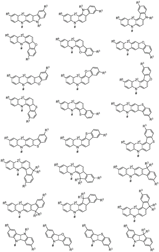

wherein the above definition applies.
Examples of the second chemical moiety according to the invention are shown below, which of course does not imply that the invention is limited to these examples:


wherein the above definition applies.
In a preferred embodiment of the invention, each TADF material E B Having the formula E B -I, formula E B -II, formula E B -III, formula E B -IV, formula E B V, E B -VI, formula E B -VII, formula E B -VIII, formula E B -IX, E B -X and E B -structure represented by any one of XI:


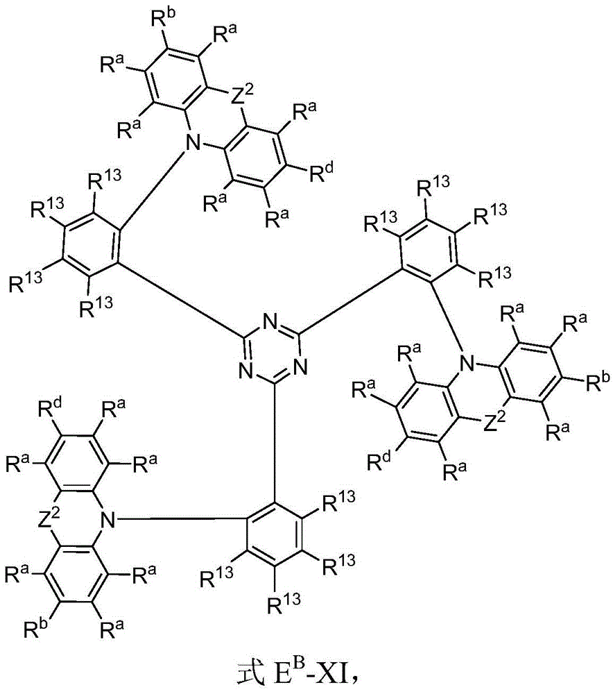
wherein,,
R 13 for example R 11 Defined, provided that R 13 A binding site that cannot be a single bond connecting the first chemical moiety or the second chemical moiety to the third chemical moiety;
R Y selected from CN and CF 3 Or R Y Comprising or consisting of a structure according to formula BN-I:

the formula BN-I is bonded to formula E via a single bond represented by a dotted line B -I, formula E B -II, formula E B -III, formula E B -IV, formula E B V, E B -VI, formula E B -VII, formula E B -VIII or formula E B -IX, and wherein exactly one R BN The radical being CN and the other two R' s BN All groups are hydrogen (H);
and wherein the above definition is applicable in addition thereto.
In a preferred embodiment of the invention, R 13 At each occurrence is hydrogen.
In one embodiment of the invention, R Y At each occurrence is CN.
In one embodiment of the invention, R Y At each occurrence is CF 3 。
In one embodiment of the invention, R Y At each occurrence is a structure represented by formula BN-I.
In a preferred embodiment of the invention, R Y Independently of each other at each occurrence is selected from CN and the structure represented by formula BN-I.
In a preferred embodiment of the invention, each TADF material E B Having the formula E B -I, formula E B -II, formula E B -III, formula E B -IV, formula E B V, E B -VI, formula E B -VII and formula E B -a structure represented by any one of X, wherein the above definition applies.
In a preferred embodiment of the invention, each TADF material E B Having the formula E B -I, formula E B -II, formula E B -III, formula E B V and formula E B -a structure represented by any one of X, wherein the above definition applies.
The following list is a list of TADF materials E used in the organic electroluminescent device according to the invention B However, this does not imply that the only examples shown are suitable TADF materials E in the context of the present invention B 。
In the following is shown a method according to formula E B TADF Material E of I B Non-limiting examples of (a):


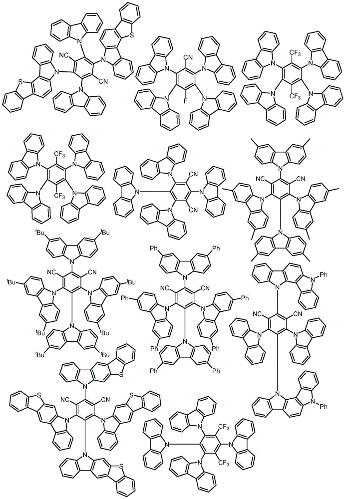

in the following is shown a method according to formula E B TADF Material E of-II B Non-limiting examples of (a):


in the following is shown a method according to formula E B TADF Material E of III B Non-limiting examples of (a):


in the following is shown a method according to formula E B TADF Material E of IV B Non-limiting examples of (a):

in the following is shown a method according to formula E B TADF Material E of V B Non-limiting examples of (a):
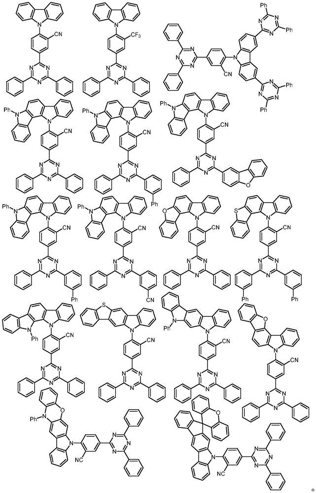
in the following is shown a method according to formula E B TADF Material E of VI B Non-limiting examples of (a):

in the following is shown a method according to formula E B TADF Material E of VII B Non-limiting examples of (a):

in the following is shown a method according to formula E B TADF Material E of VIII B Non-limiting examples of (a):

in the following is shown a method according to formula E B TADF Material E of-IX B Non-limiting examples of (a):


in the following is shown a method according to formula E B TADF Material E of-X B Non-limiting examples of (a):
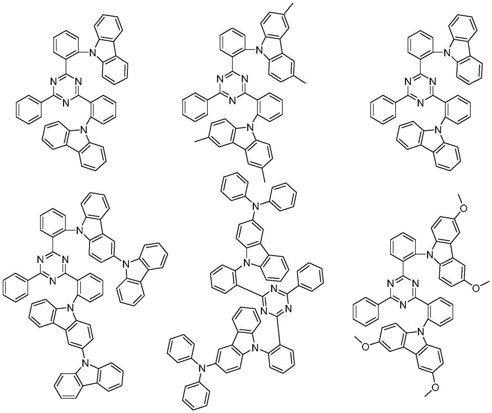

in the following is shown a method according to formula E B TADF Material E of-XI B Non-limiting examples of (a):

TADF Material E B Can be accomplished via standard reactions and reaction conditions known to those skilled in the art. Typically, in a first step, the synthesis according to formula E, shown below by way of example, may be performed B -III, formula E B -IV and formula E B TADF material E of any of-V B Is a coupling reaction (preferably, palladium catalyzed coupling reaction):
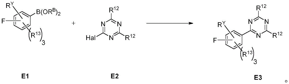
e1 can be any boric acid (R B =h) or equivalent borates (R B =alkyl or aryl), in particular, two R B A ring may be formed to give, for example, pinacol borate. E2 is used as the second reactant, wherein Hal refers to halogen and may be I, br or Cl, but is preferably Br. The reaction conditions for such palladium-catalyzed coupling reactions are known to those skilled in the art (e.g., by WO 2017/005699), and it is known that the reactive groups of E1 and E2 can be interchanged as shown below to optimize the reaction yield:

In a second step, the TADF material is obtained in nucleophilic aromatic substitution via reaction of an aza ring with an aryl halide (preferably, aryl fluoride E3). Typical conditions include the use of, for example, a base such as tripotassium phosphate or sodium hydride in, for example, an aprotic polar solvent such as dimethyl sulfoxide (DMSO) or N, N-Dimethylformamide (DMF).
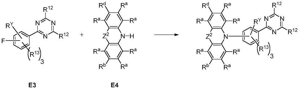
In particular, the donor molecule E4 is a 3, 6-substituted carbazole (e.g., 3, 6-dimethyl carbazole, 3, 6-diphenyl carbazole, 3, 6-di-tert-butyl carbazole), a 2, 7-substituted carbazole (e.g., 2, 7-dimethyl carbazole, 2, 7-diphenyl carbazole, 2, 7-di-tert-butyl carbazole), a 1, 8-substituted carbazole (e.g., 1, 8-dimethyl carbazole, 1, 8-diphenyl carbazole, 1, 8-di-tert-butyl carbazole), a 1-substituted carbazole (e.g., 1-methyl carbazole, 1-phenyl carbazole, 1-tert-butyl carbazole), a 2-substituted carbazole (e.g., 2-methyl carbazole, 2-phenyl carbazole, 2-tert-butyl carbazole), or a 3-substituted carbazole (e.g., 3-methyl carbazole, 3-phenyl carbazole, 3-tert-butyl carbazole).
Alternatively, halogen-substituted carbazole (in particular, 3-bromocarbazole) may be used as E4.
In subsequent reactions, a borate functional group or boric acid functional group may be illustratively introduced at the position of one or more halogen substituents introduced via E4 (e.g., via reaction with bis (pinacolato) diboron (CAS No. 73183-34-3)) to produce, for example, a corresponding carbazolylboronic acid or carbazolylboronic ester (such as carbazol-3-yl-boronic ester or carbazol-3-yl-boronic acid). Subsequently, the reaction mixture may be reacted with a corresponding halogenating reactant (e.g., R a Hal, preferably R a -Cl and R a -Br) introducing one or more substituents R a 、R b Or R is d Instead of borate groups or boric acid groups.
Alternatively, the halogen substituent may be introduced via the substituent R at the position of one or more halogen substituents via D-H a [R a -B(OH) 2 ]、R b [R b -B(OH) 2 ]Or R is d [R d -B(OH) 2 ]Is reacted with a corresponding borate to introduce one or more substituents R a 、R b Or R is d 。
Other TADF materials E can be similarly obtained B . TADF Material E B Or can be obtained by any alternative synthetic route suitable for the purpose.
Alternative synthetic routes may include the incorporation of an azacyclic ring into an aryl halide or aryl pseudohalide, preferably aryl bromide, aryl iodide, aryl triflate or aryl tosylate, via copper or palladium catalyzed coupling.
Phosphorescent material(s) P B
In the context of the present invention, phosphorescent material P B The light emission from the triplet state (i.e., the excited triplet state, typically the lowest excited triplet state T1) is obtained using the intramolecular spin-orbit interaction (heavy atom effect) caused by the metal atom. That is, the phosphorescent material P B Capable of emitting phosphorescence at room temperature (i.e., (approximately 20 ℃), typically by the corresponding P B P was used in poly (methyl methacrylate) (PMMA) at a concentration of 10 wt% B Is measured by spin-coating film.
It will be noted that while capable of emitting phosphorescence by definition, phosphorescent material P is optionally included as an optional excitation energy transfer component EET-2 in the inventive organic electroluminescent device B Preferably primarily as an "energy pump" rather than as an emitter material. That is, the phosphorescent material P included in the light emitting layer B B Preferably primarily transfer excitation energy to one or more small FWHM emitters S B The small FWHM emitter S B Which in turn serves as the primary emitter material(s). Phosphorescent material P in light-emitting layer B B Preferably not emitting light. However, it may emit light to some extent.
In general, it is understood that all phosphorescent complexes used in the prior art in organic electroluminescent devices can also be used in the organic electroluminescent devices according to the invention.
As is well known to those skilled in the art, phosphorescent material P used in organic electroluminescent devices B Typically a complex of Ir, pd, pt, au, os, eu, ru, re, ag and Cu, preferably a complex of Ir, pt and Pd, more preferably a complex of Ir and Pt in the context of the present invention. Those skilled in the art know which materials are suitable as phosphorescent materials in organic electroluminescent devices and know How to synthesize them. Furthermore, the person skilled in the art is familiar with the design principles of phosphorescent complexes for use in organic electroluminescent devices and knows how to adjust the emission of the complexes by means of structural changes.
See, for example: C. -l.ho, h.li, w. -y.wong, journal of Organometallic chemistry2014,751,261, DOI 10.1016/j.j organischem.2013.09.035; T.Fleetham, G.Li, J.Li, advanced Science News 2017,29,1601861, DOI:10.1002/adma.2016011861; A.R.B.M.Yusoff, A.J.Huckaba, M.K.Nazeeruddin, topics in Current Chemistry (Z) 2017,375:39,1, DOI:10.1007/s41061-017-0126-7; t. -Y.Li, J.Wuc, Z. -G.wua, Y. -X.zheng, J. -L.Zuo, Y.Pan, coordination Chemistry Reviews 2018,374,55, DOI:10.1016/j.ccr.2018.06.014.
For example, the number of the cells to be processed, US (A1), US20010019782 (A1), US (A1) US (A1), US (A1) US (A1), US (A1), US2013334521 (A1), US2014103305 (A1), US2003068536 (A1), US2003085646 (A1), US2006228581 (A1), US2006197077 (A1), US2011114922 (A1), US2003054198 (A1) and EP2730583 (A1) disclose that can be used as the context of the present invention Phosphorescent material P therein B Is a phosphor material of the formula (I). It is understood that this does not imply that the invention is limited to organic electroluminescent devices comprising phosphorescent materials described in one of said references.
Examples of phosphorescent complexes for use in organic electroluminescent devices such as the organic electroluminescent device of the present invention include those shown below, as described in US2020274081 (A1). Furthermore, it is understood that the invention is not limited to these examples.

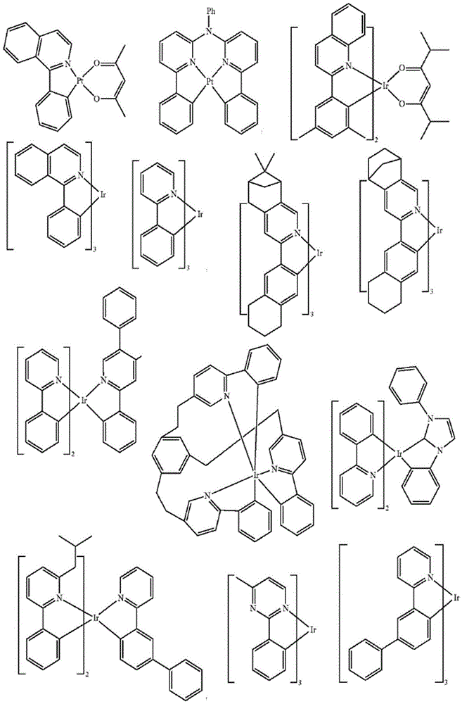


As mentioned above, one skilled in the art will recognize that any phosphorescent complex used in the prior art may be suitable as phosphorescent material P in the context of the present invention B 。
In one embodiment of the invention, each phosphor material P included in the light emitting layer B B Including iridium (Ir).
In one embodiment of the invention, at least one phosphorescent material P included in the light emitting layer B B (preferably, each phosphorescent material P B ) Is an organometallic complex that includes iridium (Ir) or platinum (Pt).
In one embodiment of the invention, at least one phosphorescent material P included in the light emitting layer B B (preferably, each phosphorescent material P B ) Is an organometallic complex that includes iridium (Ir).
In one embodiment of the invention, at least one phosphorescent material P included in the light emitting layer B B (preferably, each phosphorescent material P B ) Is an organometallic complex that includes platinum (Pt).
Phosphorescent material P B Also included by the following formula P B A compound represented by formula (I),

in P B in-I, M is selected from the group consisting of Ir, pt, pd, au, eu, ru, re, ag and Cu;
n is an integer from 1 to 3; and is also provided with
X 2 And Y 1 Each occurrence independently forms a bidentate monoanionic ligand together.
In one embodiment of the inventionIn an embodiment, each phosphor material P included in the light emitting layer B B Including according to P B The structure of-I is either represented by the formula P B The structural composition of the-I,

wherein M is selected from the group consisting of Ir, pt, pd, au, eu, ru, re, ag and Cu;
n is an integer from 1 to 3; and is also provided with
X 2 And Y 1 Each occurrence independently forms a bidentate monoanionic ligand together.
From P B Examples of the compound represented by-I include a compound represented by the following formula P B -II or formula P B -a compound represented by III:

in P B -II and formula P B In III, X 'is an aromatic ring with carbon (C) bonded to M, and Y' is a ring with nitrogen (N) coordinated to M to form a ring.
X 'and Y' combine and X 'and Y' may form a new ring. In P B in-III, Z 3 Is a bidentate ligand with two oxygens (O). In P B -II and formula P B in-III, M is preferably Ir from the viewpoint of high efficiency and long life.
In P B -II and formula P B in-III, the aromatic ring X' is, for example, C 6 -C 30 Aryl, preferably C 6 -C 16 Aryl, even more preferably C 6 -C 12 Aryl, particularly preferably C 6 -C 10 Aryl, wherein X' is optionally substituted at each occurrence with one or more substituents R E 。
In P B -II and formula P B in-III, Y' is, for example, C 2 -C 30 Heteroaryl, preferably C 2 -C 25 Heteroaryl, more preferablyOptionally C 2 -C 20 Heteroaryl, even more preferably C 2 -C 15 Heteroaryl, particularly preferably C 2 -C 10 Heteroaryl, wherein Y' is optionally substituted at each occurrence with one or more substituents R E . Further, Y' may be, for example, optionally substituted with one or more substituents R E C of (2) 1 -C 5 Heteroaryl groups.
In P B -II and formula P B in-III, bidentate ligand Z with two oxygens (O) 3 For example C with two oxygens 2 -C 30 Bidentate ligand, C with two oxygens 2 -C 25 Bidentate ligands, more preferably C with two oxygens 2 -C 20 Bidentate ligands, even more preferably C with two oxygens 2 -C 15 Bidentate ligands, particularly preferably C with two oxygens 2 -C 10 Bidentate ligand, wherein Z 3 Optionally substituted at each occurrence with one or more substituents R E . In addition, Z 3 May for example be optionally substituted with one or more substituents R E Has two oxygens C 2 -C 5 Bidentate ligands.
R E Independently of each other at each occurrence selected from the group consisting of: hydrogen; deuterium; n (R) 5E ) 2 ;OR 5E ;SR 5E ;Si(R 5E ) 3 ;CF 3 The method comprises the steps of carrying out a first treatment on the surface of the A CN; halogen; c (C) 1 -C 40 Alkyl optionally substituted with one or more substituents R 5E And wherein one or more non-adjacent CH' s 2 The radicals being optionally substituted by R 5E C=CR 5E 、C≡C、Si(R 5E ) 2 、Ge(R 5E ) 2 、Sn(R 5E ) 2 、C=O、C=S、C=Se、C=NR 5E 、P(=O)(R 5E )、SO、SO 2 、NR 5E O, S or CONR 5E Substitution; c (C) 1 -C 40 Thioalkoxy optionally substituted with one or more substituents R 5E And wherein one or more non-adjacent CH' s 2 The radicals being optionally substituted by R 5E C=CR 5E 、C≡C、Si(R 5E ) 2 、Ge(R 5E ) 2 、Sn(R 5E ) 2 、C=O、C=S、C=Se、C=NR 5E 、P(=O)(R 5E )、SO、SO 2 、NR 5E O, S or CONR 5E Substitution; c (C) 6 -C 60 Aryl optionally substituted with one or more substituents R 5E The method comprises the steps of carrying out a first treatment on the surface of the C 3 -C 57 Heteroaryl, optionally substituted with one or more substituents R 5E 。
R 5E Independently of each other at each occurrence selected from the group consisting of: hydrogen; deuterium; n (R) 6E ) 2 ;OR 6E ;SR 6E ;Si(R 6E ) 3 ;CF 3 ;CN;F;C 1 -C 40 Alkyl optionally substituted with one or more substituents R 6E And wherein one or more non-adjacent CH' s 2 The radicals being optionally substituted by R 6E C=CR 6E 、C≡C、Si(R 6E ) 2 、Ge(R 6E ) 2 、Sn(R 6E ) 2 、C=O、C=S、C=Se、C=NR 6E 、P(=O)(R 6E )、SO、SO 2 、NR 6E O, S or CONR 6E Substitution; c (C) 6 -C 60 Aryl optionally substituted with one or more substituents R 6E The method comprises the steps of carrying out a first treatment on the surface of the C 3 -C 57 Heteroaryl, optionally substituted with one or more substituents R 6E 。
R 6E Independently of each other at each occurrence selected from the group consisting of: hydrogen; deuterium; OPh; CF (compact flash) 3 ;CN;F;C 1 -C 5 Alkyl, wherein one or more hydrogen atoms are optionally replaced by deuterium, CN, CF independently of one another 3 Or F substitution; c (C) 1 -C 5 Alkoxy, wherein one or more hydrogen atoms are optionally replaced by deuterium, CN, CF independently of one another 3 Or F substitution; c (C) 1 -C 5 Thioalkoxy groups in which one or more hydrogen atoms are optionally replaced by deuterium, CN, CF independently of one another 3 Or F substitution; c (C) 6 -C 18 Aryl radicals, optionally takenSubstituted with one or more C 1 -C 5 An alkyl substituent; c (C) 3 -C 17 Heteroaryl, optionally substituted with one or more C 1 -C 5 An alkyl substituent; n (C) 6 -C 18 Aryl group 2 ;N(C 3 -C 17 Heteroaryl group 2 The method comprises the steps of carrying out a first treatment on the surface of the N (C) 3 -C 17 Heteroaryl) (C) 6 -C 18 Aryl).
Substituent R E 、R 5E Or R is 6E Independently of one another optionally can be substituted with one or more substituents R E 、R 5E 、R 6E And/or with X ', Y' and Z 3 Forming a mono-or polycyclic aliphatic, aromatic, heteroaromatic ring system.
From P B Non-limiting examples of compounds represented by-II include Ir (ppy) 3 、Ir(ppy) 2 (acac)、Ir(mppy) 3 、Ir(PPy) 2 (m-bppy)、BtpIr(acac)、Ir(btp) 2 (acac)、Ir(2-phq) 3 、Hex-Ir(phq) 3 、Ir(fbi) 2 (acac), face-tris (2- (3-p-xylyl) phenyl) iridium (III) pyridine, eu (dbm) 3 (Phen)、Ir(piq) 3 、Ir(piq) 2 (acac)、Ir(Fiq) 2 (acac)、Ir(Flq) 2 (acac)、Ru(dtb-bpy)3·2(PF 6 )、Ir(2-phq) 3 、Ir(BT) 2 (acac)、Ir(DMP) 3 、Ir(Mpq)3、Ir(phq) 2 tpy, face-Ir (ppy) 2 Pc、Ir(dp)PQ 2 、Ir(Dpm)(Piq) 2 、Hex-Ir(piq) 2 (acac)、Hex-Ir(piq) 3 、Ir(dmpq) 3 、Ir(dmpq) 2 (acac), FPQIrpic, and the like.
From P B Other non-limiting examples of compounds represented by formula II include those represented by formula P below B -II-1 to formula P B -a compound represented by II-11. In the structural formula, "Me" represents methyl.

From P B -III compoundsOther non-limiting examples of (a) include those represented by the following formula P B -III-1 to formula P B -a compound represented by III-6. In the structural formula, "Me" represents methyl.

Furthermore, iridium complexes described in US2003017361 (A1), US2004262576 (A1), WO2010027583 (A1), US2019245153 (A1), US2013119354 (A1) and US2019233451 (A1) can be used. Ir (ppy) from the viewpoint of high efficiency of phosphorescent materials 3 And Hex-Ir (ppy) 3 Are typically used for green light emission.
Exciplex
It has been demonstrated that TADF materials are capable of converting an excited triplet state (preferably T1) into an excited singlet state (preferably S1) by means of reverse intersystem crossing (RISC). It has also been demonstrated that this typically requires a small ΔE ST Values, by definition, for TADF Material E B The delta E is ST The value is less than 0.4eV.
As also illustrated, this is typically accomplished by designing TADF material E B Is achieved such that HOMO and LUMO are spatially largely separated on the (electron) donor and (electron) acceptor groups, respectively. However, a small ΔE is obtained ST Another strategy for the material of value is the formation of exciplex. As known to those skilled in the art, an exciplex is an excited state charge transfer complex (i.e., an excited state donor-acceptor complex) formed between a donor molecule and an acceptor molecule. It is also understood by those skilled in the art that the spatial separation between HOMO (on the donor molecule) and LUMO (on the acceptor molecule) in the exciplex generally results in them having a relatively small Δe ST And is generally capable of converting an excited triplet state (preferably T1) into an excited singlet state (preferably S1) by means of reverse intersystem crossing (RISC).
Indeed, as known to those skilled in the art, as noted above, a TADF material may not be just a material that is itself capable of RISC from an excited triplet state to an excited singlet state and subsequently emits TADF. The book is provided withIt is known to those skilled in the art that the TADF material may in fact also be an exciplex formed from two materials, preferably from two host materials H B Formed, more preferably, from p-host material H P And n host material H N Formed (see below), however, it is understood that the host material H B (typically H P And H N ) Itself may be a TADF material.
It will be appreciated by those skilled in the art that any materials included in the same layer (in particular, in the same EML) and materials in adjacent layers and in close proximity at the interface between these adjacent layers may together form an exciplex. Those skilled in the art know how to select pairs of exciplex forming materials (in particular, p-host H P And n main body H N Pair) and selection criteria (including HOMO and/or LUMO energy level requirements) for both components of the material pair. That is, where exciplex formation can be desired, one component (e.g., p-host material H P ) The Highest Occupied Molecular Orbital (HOMO) of (a) may be energetically higher than that of another component (e.g., n host material H N ) Has a HOMO at least 0.20eV high, and one component (e.g., p-host material H P ) The Lowest Unoccupied Molecular Orbital (LUMO) of (a) may be energetically higher than another component (e.g., n host material H N ) Is at least 0.20eV higher.
It is common knowledge of a person skilled in the art that if an exciplex is present in the EML of an organic electroluminescent device (in particular, an OLED), the exciplex may have the function of an emitter material and emit light when a voltage and a current are applied to the device. As is also generally known from the prior art, the exciplex may also be non-emissive and, if included in the EML of an organic electroluminescent device, may transfer excitation energy to the emitter material, for example.
The host materials H which together form an exciplex are listed below B In which the donor molecule (i.e., p-host H P ) May be selected from the following structures:
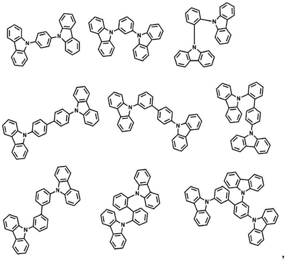
and wherein the receptor molecule (i.e., n-mer H N ) May be selected from the following structures:

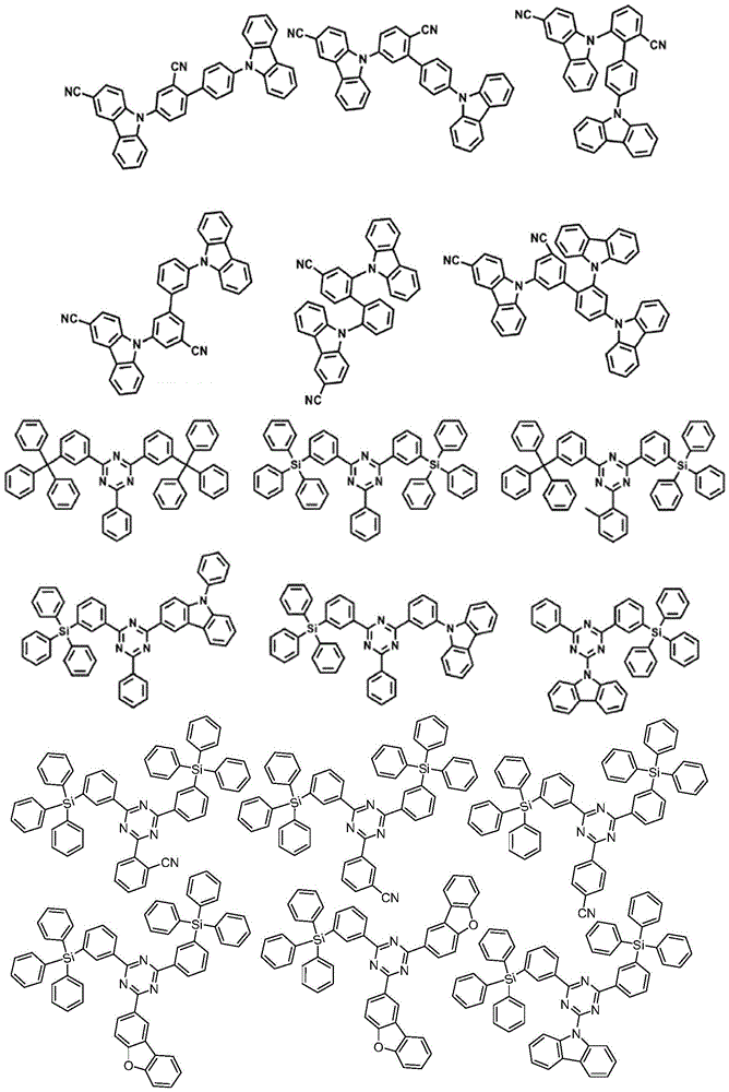

it is understood that in the context of the present invention, the exciplex may be formed of any material comprised in the light-emitting layer B, e.g. by a different excitation energy transfer component (E B And/or EET-2) is formed and is formed from an excitation energy transfer component (E) B And/or EET-2) and a small FWHM emitter S B Formed of or derived from a host material H B And an excitation energy transfer component E B Or EET-2 or small FWHM emitter S B And (5) forming. Preferably, however, they are composed of different host materials H as described above B And (5) forming. It is also understood that exciplex may also be formed and that the exciplex itself is not used as an excitation energy transfer component.
Small FWHM emitter (S) B
In the context of the present invention, a small Full Width Half Maximum (FWHM) emitter S B Is any emitter having an emission spectrum that exhibits a FWHM of less than or equal to 0.25eV (0.25 eV), measured by a spin-coating film that typically employs 1 wt.% to 5 wt.% (specifically, 2 wt.%) of the emitter in poly (methyl methacrylate) PMMA at room temperature (i.e., (approximately) 20 ℃). Alternatively, a small FWHM emitter S B The emission spectrum of (a) can be obtained in solution (typically in methylene chloride) at room temperature (i.e., (approximately) 20 ℃ C.)Use of 0.001mg/mL to 0.2mg/mL of emitter S in alkane or toluene B ) Is measured.
In a preferred embodiment of the invention, a small FWHM emitter S B Is any emitter having an emission spectrum that exhibits a FWHM of 0.24eV or less (more preferably 0.23eV or less, even more preferably 0.22eV or less, 0.21eV or 0.20eV or less) by employing 1 to 5 wt% (specifically, 2 wt%) of emitter S in PMMA at room temperature (i.e., (approximately) 20 ℃) B Is measured by spin-coating film. Alternatively, a small FWHM emitter S B Can be carried out in solution (typically with 0.001mg/mL to 0.2mg/mL of emitter S in methylene chloride or toluene) at room temperature (i.e., (approximately) 20 ℃) B ) Is measured. In other embodiments of the invention, each small FWHM emitter S B Exhibits a FWHM of 0.19eV, 0.18eV, 0.17eV, 0.16eV, 0.15eV, 0.14eV, 0.13eV, 0.12eV or 0.11 eV.
In one embodiment of the invention, each small FWHM emitter S B Emits light having an emission maximum in the wavelength range from 440 to 480nm, which is an emitter S in PMMA (1 to 5% by weight, in particular 2% by weight) at room temperature B ) Measured.
In one embodiment of the invention, each small FWHM emitter S B Emits light having an emission maximum in the wavelength range of 440nm to 480nm, which is obtained by using 0.001mg/mL to 0.2mg/mL of an emitter S in methylene chloride or toluene at room temperature (i.e., (approximately) 20 ℃) B Measured.
It is understood that TADF material E included in the light-emitting layer B of the organic electroluminescent device according to the present invention B And may alternatively be an emitter having an emission spectrum exhibiting a FWHM of less than or equal to 0.25eV (0.25 eV). Optionally, a TADF material E comprised in the light-emitting layer B of the organic electroluminescent device according to the invention B The emission maximum can also be exhibited in the above wavelength range (i.e., 440nm to 480 nm).
In one embodiment of the invention, a relationship represented by the following formula (29) applies:
440 nm ≤ λ max (S B ) ≤ 480 nm (29),
wherein lambda is max (S B ) Refers to a small FWHM emitter S in the context of the present invention B Is not shown).
In one embodiment, the above-described relationship represented by formula (29) applies to a material included in the light-emitting layer B of the organic electroluminescent device according to the invention.
In a preferred embodiment of the invention, a small FWHM emitter S B Is an organic emitter, which in the context of the invention means that it does not contain any transition metal. Preferably, a small FWHM emitter S according to the invention B Mainly composed of the elements hydrogen (H), carbon (C), nitrogen (N) and boron (B), but may also include, for example, oxygen (O), silicon (Si), fluorine (F) and bromine (Br).
In a preferred embodiment of the invention, a small FWHM emitter S B Is a fluorescent emitter, which in the context of the present invention means that upon excitation of electrons (e.g. in an electro-optical device according to the invention) the emitter is capable of emitting light at room temperature, wherein the emitted excited state is a singlet state.
In one embodiment of the invention, a small FWHM emitter S B Exhibits a photoluminescence quantum yield (PLQY) equal to or higher than 50%, which is a fraction of the emitter S in PMMA (1 to 5% by weight, in particular 2% by weight, is employed) at room temperature B ) Measured.
In a preferred embodiment of the invention, a small FWHM emitter S B Exhibits a photoluminescence quantum yield (PLQY) equal to or higher than 60%, which is a fraction of the emitter S in PMMA (1% to 5% by weight, in particular 2% by weight, is employed) at room temperature B ) Measured.
In an even more preferred embodiment of the invention, a small FWHM emitter S B Exhibits a photoluminescence quantum yield (PLQY) equal to or higher than 70%, which is a fraction of the emitter S in PMMA (1% to 5% by weight, in particular 2% by weight, is employed) at room temperature B ) Measured.
Even in the inventionIn still more preferred embodiments, a small FWHM emitter S B Exhibits a photoluminescence quantum yield (PLQY) equal to or higher than 80%, which is a fraction of the emitter S in PMMA (1% to 5% by weight, in particular 2% by weight, is employed) at room temperature B ) Measured.
In a particularly preferred embodiment of the invention, a small FWHM emitter S B Exhibits a photoluminescence quantum yield (PLQY) equal to or higher than 90%, which is a fraction of the emitter S in PMMA (1% to 5% by weight, in particular 2% by weight, is employed) at room temperature B ) Measured.
In one embodiment of the invention, a small FWHM emitter S B Exhibit a photoluminescence quantum yield (PLQY) equal to or higher than 50%, which is obtained by using 0.001mg/mL to 0.2mg/mL of emitter S in methylene chloride or toluene at room temperature (i.e., (approximately) 20 ℃) B Measured.
In a preferred embodiment of the invention, a small FWHM emitter S B Exhibit a photoluminescence quantum yield (PLQY) equal to or higher than 60%, which is obtained by using 0.001mg/mL to 0.2mg/mL of emitter S in methylene chloride or toluene at room temperature (i.e., (approximately) 20 ℃) B Measured.
In an even more preferred embodiment of the invention, a small FWHM emitter S B Exhibit a photoluminescence quantum yield (PLQY) equal to or higher than 70%, which is obtained by using 0.001mg/mL to 0.2mg/mL of emitter S in methylene chloride or toluene at room temperature (i.e., (approximately) 20 ℃) B Measured.
In an even more preferred embodiment of the invention, the small FWHM emitter S B Exhibit a photoluminescence quantum yield (PLQY) equal to or higher than 80%, which is obtained by using 0.001mg/mL to 0.2mg/mL of emitter S in methylene chloride or toluene at room temperature (i.e., (approximately) 20 ℃) B Measured.
In a particularly preferred embodiment of the invention, a small FWHM emitter S B Exhibit a photoluminescence quantum yield (PLQY) equal to or higher than 90%, which is obtained by using 0.001mg/mL to 0.2mg/mL of emitter S in methylene chloride or toluene at room temperature (i.e., (approximately) 20 ℃) B Measured.
Those skilled in the art know how to design a small FWHM emitter S that meets the above requirements or preferred characteristics B 。
Small FWHM emitters S suitable in the context of providing an invention B Another class of molecules is short-range charge transfer (NRCT) emitters.
Typical NRCT emitters are described in the literature as exhibiting a delayed component in the time resolved photoluminescence spectrum and as exhibiting a near-range HOMO-LUMO separation. See, for example: T.Hatakeyama, K.Shiren, K.Nakajima, S.Nomura, S.Nakatsuka, K.Kinoshita, J.Ni, Y.Ono, and T.Ikuta, advanced Materials 2016,28 (14), 2777, DOI:10.1002/adma.20150491.
Typical NRCT emitters show only one emission band in the emission spectrum, wherein typical fluorescent emitters show several different emission bands due to the vibrational progression.
Those skilled in the art know how to design and synthesize small FWHM emitters S that may be suitable as in the context of the present invention B Is a NRCT emitter of (c). For example, the emitter disclosed in EP3109253 (A1) can be used as a small FWHM emitter S in the context of the present invention B 。
Furthermore, for example, US2014058099 (A1), US2009295275 (A1), US2012319052 (A1), EP2182040 (A2), US2018069182 (A1), US2019393419 (A1), US2020006671 (A1), US2020098991 (A1), US2020176684 (A1), US2020161552 (A1), US2020227639 (A1), US2020185635 (A1), EP3686206 (A1), WO2020217229 (A1), WO2020208051 (A1) and US2020328351 (A1) disclose that can be suitable as a small FWHM emitter S for use in accordance with the invention B Is provided.
Small FWHM emitters S which can be used in the context of the invention B Is a boron (B) containing emitter comprising or consisting of a structure according to the following formula DABNA-I:

wherein,,
each of the rings a ', B ' and C ' independently of one another represents an aromatic or heteroaromatic ring each comprising 5 to 24 ring atoms, wherein, in the case of heteroaromatic rings, 1 to 3 ring atoms are heteroatoms independently of one another selected from N, O, S and Se; wherein,,
one or more hydrogen atoms in each of the aromatic or heteroaromatic rings A ', B ' and C ' are optionally and independently of one another substituted by substituents R DABNA-1 Substituted, substituent R DABNA-1 Independently of each other at each occurrence selected from the group consisting of: deuterium; n (R) DABNA-2 ) 2 ;OR DABNA-2 ;SR DABNA-2 ;Si(R DABNA-2 ) 3 ;B(OR DABNA-2 ) 2 ;OSO 2 R DABNA-2 ;CF 3 The method comprises the steps of carrying out a first treatment on the surface of the A CN; halogen (F, cl, br, I); c (C) 1 -C 40 Alkyl optionally substituted with one or more substituents R DABNA-2 And wherein one or more non-adjacent CH' s 2 The radicals being optionally substituted by R DABNA-2 C=CR DABNA-2 、C≡C、Si(R DABNA-2 ) 2 、Ge(R DABNA-2 ) 2 、Sn(R DABNA-2 ) 2 、C=O、C=S、C=Se、C=NR DABNA-2 、P(=O)(R DABNA-2 )、SO、SO 2 、NR DABNA-2 O, S or CONR DABNA-2 Substitution; c (C) 1 -C 40 Alkoxy optionally substituted with one or more substituents R DABNA-2 And wherein one or more non-adjacent CH' s 2 The radicals being optionally substituted by R DABNA-2 C=CR DABNA-2 、C≡C、Si(R DABNA-2 ) 2 、Ge(R DABNA-2 ) 2 、Sn(R DABNA-2 ) 2 、C=O、C=S、C=Se、C=NR DABNA-2 、P(=O)(R DABNA-2 )、SO、SO 2 、NR DABNA-2 O, S or CONR DABNA-2 Substitution; c (C) 1 -C 40 Thioalkoxy optionally substituted with one or more substituents R DABNA-2 And wherein one or more non-adjacent CH' s 2 The groups being optionalGround cover R DABNA-2 C=CR DABNA-2 、C≡C、Si(R DABNA-2 ) 2 、Ge(R DABNA-2 ) 2 、Sn(R DABNA-2 ) 2 、C=O、C=S、C=Se、C=NR DABNA-2 、P(=O)(R DABNA-2 )、SO、SO 2 、NR DABNA-2 O, S or CONR DABNA-2 Substitution; c (C) 2 -C 40 Alkenyl optionally substituted with one or more substituents R DABNA-2 And wherein one or more non-adjacent CH' s 2 The radicals being optionally substituted by R DABNA-2 C=CR DABNA-2 、C≡C、Si(R DABNA-2 ) 2 、Ge(R DABNA-2 ) 2 、Sn(R DABNA-2 ) 2 、C=O、C=S、C=Se、C=NR DABNA-2 、P(=O)(R DABNA-2 )、SO、SO 2 、NR DABNA-2 O, S or CONR DABNA-2 Substitution; c (C) 2 -C 40 Alkynyl, optionally substituted with one or more substituents R DABNA-2 And wherein one or more non-adjacent CH' s 2 The radicals being optionally substituted by R DABNA-2 C=CR DABNA-2 、Si(R DABNA-2 ) 2 、Ge(R DABNA-2 ) 2 、Sn(R DABNA-2 ) 2 、C=O、C=S、C=Se、C=NR DABNA-2 、P(=O)(R DABNA-2 )、SO、SO 2 、NR DABNA-2 O, S or CONR DABNA-2 Substitution; c (C) 6 -C 60 Aryl optionally substituted with one or more substituents R DABNA-2 ;C 3 -C 57 Heteroaryl, optionally substituted with one or more substituents R DABNA-2 The method comprises the steps of carrying out a first treatment on the surface of the And aliphatic cyclic amines, including 4 to 18 carbon atoms and 1 to 3 nitrogen atoms;
R DABNA-2 independently of each other at each occurrence selected from the group consisting of: hydrogen; deuterium; n (R) DABNA-6 ) 2 ;OR DABNA-6 ;SR DABNA-6 ;Si(R DABNA-6 ) 3 ;B(OR DABNA-6 ) 2 ;OSO 2 R DABNA-6 ;CF 3 The method comprises the steps of carrying out a first treatment on the surface of the A CN; halogen (F, cl, br, I); c (C) 1 -C 5 Alkyl optionally substituted with one or more substituents R DABNA-6 And wherein one or more non-adjacent CH' s 2 The radicals being optionally substituted by R DABNA-6 C=CR DABNA-6 、C≡C、Si(R DABNA-6 ) 2 、Ge(R DABNA-6 ) 2 、Sn(R DABNA-6 ) 2 、C=O、C=S、C=Se、C=NR DABNA-6 、P(=O)(R DABNA-6 )、SO、SO 2 、NR DABNA-6 O, S or CONR DABNA-6 Substitution; c (C) 1 -C 5 Alkoxy optionally substituted with one or more substituents R DABNA-6 And wherein one or more non-adjacent CH' s 2 The radicals being optionally substituted by R DABNA-6 C=CR DABNA-6 、C≡C、Si(R DABNA-6 ) 2 、Ge(R DABNA-6 ) 2 、Sn(R DABNA-6 ) 2 、C=O、C=S、C=Se、C=NR DABNA-6 、P(=O)(R DABNA-6 )、SO、SO 2 、NR DABNA-6 O, S or CONR DABNA-6 Substitution; c (C) 1 -C 5 Thioalkoxy optionally substituted with one or more substituents R DABNA-6 And wherein one or more non-adjacent CH' s 2 The radicals being optionally substituted by R DABNA-6 C=CR DABNA-6 、C≡C、Si(R DABNA-6 ) 2 、Ge(R DABNA-6 ) 2 、Sn(R DABNA-6 ) 2 、C=O、C=S、C=Se、C=NR DABNA-6 、P(=O)(R DABNA-6 )、SO、SO 2 、NR DABNA-6 O, S or CONR DABNA-6 Substitution; c (C) 2 -C 5 Alkenyl optionally substituted with one or more substituents R DABNA-6 And wherein one or more non-adjacent CH' s 2 The radicals being optionally substituted by R DABNA-6 C=CR DABNA-6 、C≡C、Si(R DABNA-6 ) 2 、Ge(R DABNA-6 ) 2 、Sn(R DABNA-6 ) 2 、C=O、C=S、C=Se、C=NR DABNA-6 、P(=O)(R DABNA-6 )、SO、SO 2 、NR DABNA-6 O, S or CONR DABNA-6 Substitution; c (C) 2 -C 5 Alkynyl, optionally substituted with one or more substituents R DABNA-6 And wherein one or more non-adjacent CH' s 2 The radicals being optionally substituted by R DABNA-6 C=CR DABNA-6 、Si(R DABNA-6 ) 2 、Ge(R DABNA-6 ) 2 、Sn(R DABNA-6 ) 2 、C=O、C=S、C=Se、C=NR DABNA-6 、P(=O)(R DABNA-6 )、SO、SO 2 、NR DABNA-6 O, S or CONR DABNA-6 Substitution; c (C) 6 -C 18 Aryl optionally substituted with one or more substituents R DABNA-6 ;C 3 -C 17 Heteroaryl, optionally substituted with one or more substituents R DABNA-6 The method comprises the steps of carrying out a first treatment on the surface of the And aliphatic cyclic amines, including 4 to 18 carbon atoms and 1 to 3 nitrogen atoms;
wherein is selected from R DABNA-1 And R is DABNA-2 Optionally forming a mono-or polycyclic aliphatic or aromatic or heteroaromatic carbocyclic or heterocyclic ring system fused to adjacent ring a ', ring B' or ring C ', wherein the fused ring system optionally so formed (i.e., the corresponding ring a', ring B 'or ring C' and optionally the additional ring(s) fused thereto) comprises a total of 8 to 30 ring atoms;
Y a And Y b Independently of each other, from direct (mono) bonds, NR DABNA-3 、O、S、C(R DABNA-3 ) 2 、Si(R DABNA-3 ) 2 、BR DABNA-3 And Se;
R DABNA-3 independently of each other at each occurrence selected from the group consisting of: hydrogen; deuterium; n (R) DABNA-4 ) 2 ;OR DABNA-4 ;SR DABNA-4 ;Si(R DABNA-4 ) 3 ;B(OR DABNA-4 ) 2 ;OSO 2 R DABNA-4 ;CF 3 The method comprises the steps of carrying out a first treatment on the surface of the A CN; halogen (F, cl, br, I); c (C) 1 -C 40 Alkyl optionally substituted with one or more substituents R DABNA-4 And wherein one or more non-adjacent CH' s 2 Groups are optionallyQuilt R DABNA-4 C=CR DABNA-4 、C≡C、Si(R DABNA-4 ) 2 、Ge(R DABNA-4 ) 2 、Sn(R DABNA-4 ) 2 、C=O、C=S、C=Se、C=NR DABNA-4 、P(=O)(R DABNA-4 )、SO、SO 2 、NR DABNA-4 O, S or CONR DABNA-4 Substitution; c (C) 1 -C 40 Alkoxy optionally substituted with one or more substituents R DABNA-4 And wherein one or more non-adjacent CH' s 2 The radicals being optionally substituted by R DABNA-4 C=CR DABNA-4 、C≡C、Si(R DABNA-4 ) 2 、Ge(R DABNA-4 ) 2 、Sn(R DABNA-4 ) 2 、C=O、C=S、C=Se、C=NR DABNA-4 、P(=O)(R DABNA-4 )、SO、SO 2 、NR DABNA-4 O, S or CONR DABNA-4 Substitution; c (C) 1 -C 40 Thioalkoxy optionally substituted with one or more substituents R DABNA-4 And wherein one or more non-adjacent CH' s 2 The radicals being optionally substituted by R DABNA-4 C=CR DABNA-4 、C≡C、Si(R DABNA-4 ) 2 、Ge(R DABNA-4 ) 2 、Sn(R DABNA-4 ) 2 、C=O、C=S、C=Se、C=NR DABNA-4 、P(=O)(R DABNA-4 )、SO、SO 2 、NR DABNA-4 O, S or CONR DABNA-4 Substitution; c (C) 2 -C 40 Alkenyl optionally substituted with one or more substituents R DABNA-4 And wherein one or more non-adjacent CH' s 2 The radicals being optionally substituted by R DABNA-4 C=CR DABNA-4 、C≡C、Si(R DABNA-4 ) 2 、Ge(R DABNA-4 ) 2 、Sn(R DABNA-4 ) 2 、C=O、C=S、C=Se、C=NR DABNA-4 、P(=O)(R DABNA-4 )、SO、SO 2 、NR DABNA-4 O, S or CONR DABNA-4 Substitution; c (C) 2 -C 40 Alkynyl, optionally substituted with one or more substituents R DABNA-4 And wherein one or more non-adjacent CH 2 The radicals being optionally substituted by R DABNA-4 C=CR DABNA-4 、Si(R DABNA-4 ) 2 、Ge(R DABNA-4 ) 2 、Sn(R DABNA-4 ) 2 、C=O、C=S、C=Se、C=NR DABNA-4 、P(=O)(R DABNA-4 )、SO、SO 2 、NR DABNA-4 O, S or CONR DABNA-4 Substitution; c (C) 6 -C 60 Aryl optionally substituted with one or more substituents R DABNA-4 ;C 3 -C 57 Heteroaryl, optionally substituted with one or more substituents R DABNA-4 The method comprises the steps of carrying out a first treatment on the surface of the And aliphatic cyclic amines, including 4 to 18 carbon atoms and 1 to 3 nitrogen atoms;
R DABNA-4 independently of each other at each occurrence selected from the group consisting of: hydrogen; deuterium; n (R) DABNA-5 ) 2 ;OR DABNA-5 ;SR DABNA-5 ;Si(R DABNA-5 ) 3 ;B(OR DABNA-5 ) 2 ;OSO 2 R DABNA-5 ;CF 3 The method comprises the steps of carrying out a first treatment on the surface of the A CN; halogen (F, cl, br, I); c (C) 1 -C 40 Alkyl optionally substituted with one or more substituents R DABNA-5 And wherein one or more non-adjacent CH' s 2 The radicals being optionally substituted by R DABNA-5 C=CR DABNA-5 、C≡C、Si(R DABNA-5 ) 2 、Ge(R DABNA-5 ) 2 、Sn(R DABNA-5 ) 2 、C=O、C=S、C=Se、C=NR DABNA-5 、P(=O)(R DABNA-5 )、SO、SO 2 、NR DABNA-5 O, S or CONR DABNA-5 Substitution; c (C) 1 -C 40 Alkoxy optionally substituted with one or more substituents R DABNA-5 And wherein one or more non-adjacent CH' s 2 The radicals being optionally substituted by R DABNA-5 C=CR DABNA-5 、C≡C、Si(R DABNA-5 ) 2 、Ge(R DABNA-5 ) 2 、Sn(R DABNA-5 ) 2 、C=O、C=S、C=Se、C=NR DABNA-5 、P(=O)(R DABNA-5 )、SO、SO 2 、NR DABNA-5 O, S or CONR DABNA-5 Substitution; c (C) 1 -C 40 Thioalkoxy optionally substituted with one or more substituents R DABNA-5 And wherein one or more non-adjacent CH' s 2 The radicals being optionally substituted by R DABNA-5 C=CR DABNA-5 、C≡C、Si(R DABNA-5 ) 2 、Ge(R DABNA-5 ) 2 、Sn(R DABNA-5 ) 2 、C=O、C=S、C=Se、C=NR DABNA-5 、P(=O)(R DABNA-5 )、SO、SO 2 、NR DABNA-5 O, S or CONR DABNA-5 Substitution; c (C) 2 -C 40 Alkenyl optionally substituted with one or more substituents R DABNA-5 And wherein one or more non-adjacent CH' s 2 The radicals being optionally substituted by R DABNA-5 C=CR DABNA-5 、C≡C、Si(R DABNA-5 ) 2 、Ge(R DABNA-5 ) 2 、Sn(R DABNA-5 ) 2 、C=O、C=S、C=Se、C=NR DABNA-5 、P(=O)(R DABNA-5 )、SO、SO 2 、NR DABNA-5 O, S or CONR DABNA-5 Substitution; c (C) 2 -C 40 Alkynyl, optionally substituted with one or more substituents R DABNA-5 And wherein one or more non-adjacent CH' s 2 The radicals being optionally substituted by R DABNA-5 C=CR DABNA-5 、Si(R DABNA-5 ) 2 、Ge(R DABNA-5 ) 2 、Sn(R DABNA-5 ) 2 、C=O、C=S、C=Se、C=NR DABNA-5 、P(=O)(R DABNA-5 )、SO、SO 2 、NR DABNA-5 O, S or CONR DABNA-5 Substitution; c (C) 6 -C 60 Aryl optionally substituted with one or more substituents R DABNA-5 ;C 3 -C 57 Heteroaryl, optionally substituted with one or more substituents R DABNA-5 The method comprises the steps of carrying out a first treatment on the surface of the And aliphatic cyclic amines, including 4 to 18 carbon atoms and 1 to 3 nitrogen atoms;
R DABNA-5 independently of each other at each occurrence selected from the group consisting of: hydrogen; deuterium; n (R) DABNA-6 ) 2 ;OR DABNA-6 ;SR DABNA-6 ;Si(R DABNA-6 ) 3 ;B(OR DABNA-6 ) 2 ;OSO 2 R DABNA-6 ;CF 3 The method comprises the steps of carrying out a first treatment on the surface of the A CN; halogen (F, cl, br, I); c (C) 1 -C 5 Alkyl optionally substituted with one or more substituents R DABNA-6 And wherein one or more non-adjacent CH' s 2 The radicals being optionally substituted by R DABNA-6 C=CR DABNA-6 、C≡C、Si(R DABNA-6 ) 2 、Ge(R DABNA-6 ) 2 、Sn(R DABNA-6 ) 2 、C=O、C=S、C=Se、C=NR DABNA-6 、P(=O)(R DABNA-6 )、SO、SO 2 、NR DABNA-6 O, S or CONR DABNA-6 Substitution; c (C) 1 -C 5 Alkoxy optionally substituted with one or more substituents R DABNA-6 And wherein one or more non-adjacent CH' s 2 The radicals being optionally substituted by R DABNA-6 C=CR DABNA-6 、C≡C、Si(R DABNA-6 ) 2 、Ge(R DABNA-6 ) 2 、Sn(R DABNA-6 ) 2 、C=O、C=S、C=Se、C=NR DABNA-6 、P(=O)(R DABNA-6 )、SO、SO 2 、NR DABNA-6 O, S or CONR DABNA-6 Substitution; c (C) 1 -C 5 Thioalkoxy optionally substituted with one or more substituents R DABNA-6 And wherein one or more non-adjacent CH' s 2 The radicals being optionally substituted by R DABNA-6 C=CR DABNA-6 、C≡C、Si(R DABNA-6 ) 2 、Ge(R DABNA-6 ) 2 、Sn(R DABNA-6 ) 2 、C=O、C=S、C=Se、C=NR DABNA-6 、P(=O)(R DABNA-6 )、SO、SO 2 、NR DABNA-6 O, S or CONR DABNA-6 Substitution; c (C) 2 -C 5 Alkenyl optionally substituted with one or more substituents R DABNA-6 And wherein one or more non-adjacent CH' s 2 The radicals being optionally substituted by R DABNA-6 C=CR DABNA-6 、C≡C、Si(R DABNA-6 ) 2 、Ge(R DABNA-6 ) 2 、Sn(R DABNA-6 ) 2 、C=O、C=S、C=Se、C=NR DABNA-6 、P(=O)(R DABNA-6 )、SO、SO 2 、NR DABNA-6 O, S or CONR DABNA-6 Substitution; c (C) 2 -C 5 Alkynyl, optionally substituted with one or more substituents R DABNA-6 And wherein one or more non-adjacent CH' s 2 The radicals being optionally substituted by R DABNA-6 C=CR DABNA-6 、Si(R DABNA-6 ) 2 、Ge(R DABNA-6 ) 2 、Sn(R DABNA-6 ) 2 、C=O、C=S、C=Se、C=NR DABNA-6 、P(=O)(R DABNA-6 )、SO、SO 2 、NR DABNA-6 O, S or CONR DABNA-6 Substitution; c (C) 6 -C 18 Aryl optionally substituted with one or more substituents R DABNA-6 ;C 3 -C 17 Heteroaryl, optionally substituted with one or more substituents R DABNA-6 The method comprises the steps of carrying out a first treatment on the surface of the And aliphatic cyclic amines, including 4 to 18 carbon atoms and 1 to 3 nitrogen atoms;
wherein is selected from R DABNA-3 、R DABNA-4 And R is DABNA-5 Optionally forming a mono-or polycyclic aliphatic or aromatic or heteroaromatic carbocyclic or heterocyclic ring system with each other, wherein the ring system optionally so formed comprises a total of 8 to 30 ring atoms;
R DABNA-6 independently of each other at each occurrence selected from the group consisting of: hydrogen; deuterium; OPh (ph=phenyl); SPh; CF (compact flash) 3 ;CN;F;Si(C 1 -C 5 Alkyl group 3 ;Si(Ph) 3 ;C 1 -C 5 Alkyl, wherein optionally one or more hydrogen atoms are independently replaced by deuterium, ph, CN, CF 3 Or F substitution; c (C) 1 -C 5 Alkoxy, wherein optionally one or more hydrogen atoms are independently replaced by deuterium, CN, CF 3 Or F substitution; c (C) 1 -C 5 Thioalkoxy groups in which optionally one or more hydrogen atoms are independently replaced by deuterium, CN, CF 3 Or F substitution; c (C) 2 -C 5 Alkenyl groups, wherein,optionally one or more hydrogen atoms are independently replaced by deuterium, CN, CF 3 Or F substitution; c (C) 2 -C 5 Alkynyl, wherein optionally one or more hydrogen atoms are independently replaced by deuterium, CN, CF 3 Or F substitution; c (C) 6 -C 18 Aryl wherein optionally one or more hydrogen atoms are independently replaced by deuterium, CN, CF 3 、F、C 1 -C 5 Alkyl, siMe 3 、SiPh 3 Or C 6 -C 18 Aryl substituent substitution; c (C) 3 -C 17 Heteroaryl, wherein optionally one or more hydrogen atoms are independently replaced by deuterium, CN, CF 3 、F、C 1 -C 5 Alkyl, siMe 3 、SiPh 3 Or C 6 -C 18 Aryl substituent substitution; n (C) 6 -C 18 Aryl group 2 ;N(C 3 -C 17 Heteroaryl group 2 The method comprises the steps of carrying out a first treatment on the surface of the N (C) 3 -C 17 Heteroaryl) (C) 6 -C 18 An aryl group);
wherein at Y a And Y b One or Y of a And Y b Both are NR DABNA-3 、C(R DABNA-3 ) 2 、Si(R DABNA-3 ) 2 Or BR DABNA-3 In the case of (a), one or two substituents R DABNA-3 Can be selected in each case optionally and independently of one another via a direct (mono) bond or via an NR independently of one another DABNA-1 、O、S、C(R DABNA-1 ) 2 、Si(R DABNA-1 ) 2 、BR DABNA-1 And Se are bonded to adjacent ring A 'and ring B' (for Y) a =NR DABNA-3 、C(R DABNA-3 ) 2 、Si(R DABNA-3 ) 2 Or BR DABNA-3 ) Or ring a 'and ring C' (for Y) b =NR DABNA-3 、C(R DABNA-3 ) 2 、Si(R DABNA-3 ) 2 Or BR DABNA-3 ) One or both of which;
and wherein, optionally, two or more structures of formula DABNA-I (preferably, two structures of formula DABNA-I) are conjugated to each other (preferably, fused to each other by sharing at least one bond (more preferably, exactly one bond);
wherein, optionally, two or more structures of formula DABA-I (preferably, two structures of formula DABA-I) are present in the emitter and share at least one (preferably, exactly one) aromatic or heteroaromatic ring (i.e., the ring may be part of two structures of formula DABA-I), at least one (preferably, exactly one) aromatic or heteroaromatic ring is preferably any of rings A ', B ' and C ' of formula DABA-I, but may also be selected from R DABNA-1 、R DABNA-2 、R DABNA-3 、R DABNA-4 、R DABNA-5 And R is DABNA-6 Any aromatic or heteroaromatic substituent (in particular, R DABNA-3 ) Or any aromatic or heteroaromatic ring formed from two or more adjacent substituents as described above, wherein the shared ring may constitute the same or different parts of the structure of two or more DABNA-I of the shared ring (i.e. the shared ring may be, for example, a ring C ' of two structures of DABNA-I of the formula optionally included in the emitter, or the shared ring may be, for example, a ring B ' of one structure and a ring C ' of another structure of DABNA-I of the formula optionally included in the emitter); and is also provided with
Wherein, optionally, R DABNA-1 、R DABNA-2 、R DABNA-3 、R DABNA-4 、R DABNA-5 And R is DABNA-6 Is replaced by a bond to a further chemical entity of the formula DABA-I, and/or wherein, optionally, R DABNA-1 、R DABNA-2 、R DABNA-3 、R DABNA-4 、R DABNA-5 And R is DABNA-6 At least one hydrogen atom of any of which is replaced by a bond to a further chemical entity of the formula DABNA-I.
In one embodiment of the invention, in at least one (preferably each) light emitting layer B, one or more small FWHM emitters S B Comprises a structure according to the formula DABA-I.
In one embodiment of the invention, in at least one (preferably each) light emitting layer B, each small FWHM emitter S B Including rootAccording to the structure of formula DABA-I.
In one embodiment of the invention, in at least one (preferably each) light emitting layer B, one or more small FWHM emitters S B Is composed of a structure according to the formula DABA-I.
In one embodiment of the invention, in at least one (preferably each) light emitting layer B, each small FWHM emitter S B Consists of a structure according to formula DABA-I.
In a preferred embodiment of the invention, wherein in at least one (preferably each) light-emitting layer B, one or more small FWHM emitters S B Comprises or consists of a structure according to formula DABNA-I, ring a ', ring B ' and ring C ' are all aromatic rings (i.e. they are all benzene rings) having 6 ring atoms.
In one embodiment of the invention, wherein in at least one (preferably each) light emitting layer B, one or more small FWHM emitters S B At least one (preferably each) of (a) comprises or consists of a structure according to formula DABA-I, Y a And Y b Independently of one another selected from NR DABNA-3 、O、S、C(R DABNA-3 ) 2 And Si (R) DABNA-3 ) 2 。
In a preferred embodiment of the invention, wherein in at least one (preferably each) light-emitting layer B, one or more small FWHM emitters S B At least one (preferably each) of (a) comprises or consists of a structure according to formula DABA-I, Y a And Y b Independently of one another selected from NR DABNA-3 O and S.
In an even more preferred embodiment of the invention, wherein in at least one (preferably each) light emitting layer B, one or more small FWHM emitters S B At least one (preferably each) of (a) comprises or consists of a structure according to formula DABA-I, Y a And Y b Independently of one another selected from NR DABNA-3 And O.
In a particularly preferred embodiment of the inventionIn an example, wherein in at least one (preferably each) light emitting layer B, one or more small FWHM emitters S B At least one (preferably each) of (a) comprises or consists of a structure according to formula DABA-I, Y a And Y b Both are NR DABNA-3 。
In a particularly preferred embodiment of the invention, wherein in at least one (preferably each) light-emitting layer B, one or more small FWHM emitters S B At least one (preferably each) of (a) comprises or consists of a structure according to formula DABA-I, Y a And Y b Identical and both are NR DABNA-3 。
In one embodiment of the invention, wherein in at least one (preferably each) light emitting layer B, one or more small FWHM emitters S B At least one (preferably each) of which comprises or consists of a structure according to formula DABNA-I,
R DABNA-1 independently of each other at each occurrence selected from the group consisting of: hydrogen; deuterium; n (R) DABNA-2 ) 2 ;OR DABNA-2 ;SR DABNA-2 ;Si(R DABNA-2 ) 3 ;CF 3 ;CN;F;C 1 -C 5 Alkyl optionally substituted with one or more substituents R DABNA-2 ;C 1 -C 5 Alkoxy optionally substituted with one or more substituents R DABNA-2 ;C 1 -C 5 Thioalkoxy optionally substituted with one or more substituents R DABNA-2 ;C 6 -C 18 Aryl optionally substituted with one or more substituents R DABNA-2 The method comprises the steps of carrying out a first treatment on the surface of the C 3 -C 17 Heteroaryl, optionally substituted with one or more substituents R DABNA-2 ;
R DABNA-2 Independently of each other at each occurrence selected from the group consisting of: hydrogen; deuterium; n (R) DABNA-6 ) 2 ;OR DABNA-6 ;SR DABNA-6 ;Si(R DABNA-6 ) 3 ;CF 3 ;CN;F;C 1 -C 5 Alkyl optionally substituted with one or more substituents R DABNA-6 ;C 6 -C 18 Aryl optionally substituted with one or more substituents R DABNA-6 The method comprises the steps of carrying out a first treatment on the surface of the C 3 -C 17 Heteroaryl, optionally substituted with one or more substituents R DABNA-6 ;
Wherein is selected from R DABNA-1 And R is DABNA-2 Optionally forming a mono-or polycyclic aliphatic or aromatic or heteroaromatic carbocyclic or heterocyclic ring system fused to adjacent ring a ', ring B' or ring C ', wherein the fused ring system optionally so formed (i.e., the corresponding ring a', ring B 'or ring C', and optionally the additional ring(s) fused thereto) comprises a total of 8 to 30 ring atoms.
In one embodiment of the invention, wherein in at least one (preferably each) light emitting layer B, one or more small FWHM emitters S B At least one (preferably each) of which comprises or consists of a structure according to formula DABNA-I,
R DABNA-1 independently of each other at each occurrence selected from the group consisting of: hydrogen; deuterium; n (R) DABNA-2 ) 2 ;OR DABNA-2 ;SR DABNA-2 ;Si(R DABNA-2 ) 3 ;C 1 -C 5 Alkyl optionally substituted with one or more substituents R DABNA-2 ;C 6 -C 18 Aryl optionally substituted with one or more substituents R DABNA-2 The method comprises the steps of carrying out a first treatment on the surface of the C 3 -C 17 Heteroaryl, optionally substituted with one or more substituents R DABNA-2 ;
R DABNA-2 Independently of each other at each occurrence selected from the group consisting of: hydrogen; deuterium; n (R) DABNA-6 ) 2 ;OR DABNA-6 ;SR DABNA-6 ;Si(R DABNA-6 ) 3 ;CF 3 ;CN;F;C 1 -C 5 Alkyl optionally substituted with one or more substituents R DABNA-6 ;C 6 -C 18 Aryl optionally substituted with one or more fetchesSubstituent R DABNA-6 The method comprises the steps of carrying out a first treatment on the surface of the C 3 -C 17 Heteroaryl, optionally substituted with one or more substituents R DABNA-6 ;
Wherein is selected from R DABNA-1 And R is DABNA-2 Optionally forming a mono-or polycyclic aliphatic or aromatic or heteroaromatic carbocyclic or heterocyclic ring system fused to adjacent ring a ', ring B' or ring C ', wherein the fused ring system optionally so formed (i.e., the corresponding ring a', ring B 'or ring C', and optionally the additional ring(s) fused thereto) comprises a total of 8 to 30 ring atoms.
In one embodiment of the invention, wherein in at least one (preferably each) light emitting layer B, one or more small FWHM emitters S B At least one (preferably each) of which comprises or consists of a structure according to formula DABNA-I,
R DABNA-1 independently of each other at each occurrence selected from the group consisting of: hydrogen; deuterium; n (R) DABNA-2 ) 2 ;OR DABNA-2 ;SR DABNA-2 ;C 1 -C 5 Alkyl optionally substituted with one or more substituents R DABNA-2 ;C 6 -C 18 Aryl optionally substituted with one or more substituents R DABNA-2 The method comprises the steps of carrying out a first treatment on the surface of the C 3 -C 17 Heteroaryl, optionally substituted with one or more substituents R DABNA-2 ;
R DABNA-2 Independently of each other at each occurrence selected from the group consisting of: hydrogen; deuterium; n (Ph) 2 ;OPh;CN;Me; i Pr; t Bu;Si(Me) 3 The method comprises the steps of carrying out a first treatment on the surface of the Ph, optionally substituted with one or more substituents R DABNA-6 The method comprises the steps of carrying out a first treatment on the surface of the C 3 -C 17 Heteroaryl, optionally substituted with one or more substituents R DABNA-6 ;
Wherein two or more adjacent R' s DABNA-1 Forming a mono-or polycyclic, aliphatic or aromatic or heteroaromatic, carbocyclic or heterocyclic ring system fused to adjacent rings A ', B ' or C ', wherein optionallyThe fused ring system so formed (i.e., the corresponding ring a ', ring B ' or ring C ' and optionally the additional ring(s) fused thereto) comprises a total of 8 to 30 ring atoms.
In one embodiment of the invention, wherein in at least one (preferably each) light emitting layer B, one or more small FWHM emitters S B At least one (preferably each) of which comprises or consists of a structure according to formula DABNA-I,
R DABNA-1 independently of each other at each occurrence selected from the group consisting of: hydrogen; deuterium; n (Ph) 2 ;OPh;Me; i Pr; t Bu;Si(Me) 3 The method comprises the steps of carrying out a first treatment on the surface of the Ph, wherein one or more hydrogen atoms are optionally replaced independently of each other by deuterium, me, i Pr、 t Bu, ph or CN; c 3 -C 17 Heteroaryl, wherein one or more hydrogen atoms are optionally substituted independently of each other by deuterium, me, i Pr、 t Bu, ph or CN;
wherein two or more adjacent substituents R DABNA-1 Optionally forming a mono-or polycyclic aliphatic or aromatic or heteroaromatic carbocyclic or heterocyclic ring system fused to adjacent ring a ', ring B' or ring C ', wherein the fused ring system optionally so formed (i.e. the corresponding ring a', ring B 'or ring C' and optionally the additional ring(s) fused thereto) comprises a total of 8 to 30 ring atoms.
In one embodiment of the invention, wherein in at least one (preferably each) light emitting layer B, one or more small FWHM emitters S B At least one (preferably each) of which comprises or consists of a structure according to formula DABNA-I,
R DABNA-1 Independently of each other at each occurrence selected from the group consisting of: hydrogen; deuterium; n (Ph) 2 ;Me; i Pr; t Bu; ph, wherein one or more hydrogen atoms are optionally replaced independently of each other by deuterium, me, i Pr、 t Bu, ph or CN; carbazolyl groups in which one or more hydrogen atoms are optionally substituted independently of one another by deuterium, me, i Pr、 t Bu, ph or CN; triazinyl groups in which one or more hydrogen atoms are optionally replaced independently of one another by deuterium, me, i Pr、 t Bu or Ph substitution; pyrimidinyl wherein one or more hydrogen atoms are optionally replaced independently of each other by deuterium, me, i Pr、 t Bu or Ph substitution; and pyridyl, wherein one or more hydrogen atoms are optionally replaced by deuterium, me, i Pr、 t bu or Ph substitution;
wherein two or more adjacent substituents R DABNA-1 Optionally forming a mono-or polycyclic aliphatic or aromatic or heteroaromatic carbocyclic or heterocyclic ring system fused to adjacent ring a ', ring B' or ring C ', wherein the fused ring system optionally so formed (i.e. the corresponding ring a', ring B 'or ring C' and optionally the additional ring(s) fused thereto) comprises a total of 8 to 30 ring atoms.
In one embodiment of the invention, wherein in at least one (preferably each) light emitting layer B, one or more small FWHM emitters S B At least one (preferably each) of (or consists of) a structure according to formula DABA-I selected from R DABNA-1 And R is DABNA-2 The adjacent substituents of (a) do not form a mono-or polycyclic aliphatic or aromatic or heteroaromatic carbocyclic or heterocyclic ring system fused to the adjacent ring a ', ring B ' or ring C '.
In one embodiment of the invention, wherein in at least one (preferably each) light emitting layer B, one or more small FWHM emitters S B At least one (preferably each) of which comprises or consists of a structure according to formula DABNA-I,
R DABNA-3 independently of each other at each occurrence selected from the group consisting of: hydrogen; deuterium; c (C) 1 -C 4 Alkyl optionally substituted with one or more substituents R DABNA-4 ;C 6 -C 18 Aryl optionally substituted with one or more substituents R DABNA-4 The method comprises the steps of carrying out a first treatment on the surface of the C 3 -C 17 Heteroaryl optionally substituted with one or more extractablesSubstituent R DABNA-4 ;
R DABNA-4 Independently of each other at each occurrence selected from the group consisting of: hydrogen; deuterium; n (R) DABNA-5 ) 2 ;OR DABNA-5 ;SR DABNA-5 ;Si(C 1 -C 5 Alkyl group 3 ;CF 3 ;CN;F;C 1 -C 5 Alkyl optionally substituted with one or more substituents R DABNA-5 ;C 6 -C 18 Aryl optionally substituted with one or more substituents R DABNA-5 The method comprises the steps of carrying out a first treatment on the surface of the C 3 -C 17 Heteroaryl, optionally substituted with one or more substituents R DABNA-5 ;
R DABNA-5 Independently of each other at each occurrence selected from the group consisting of: hydrogen; deuterium; n (Ph) 2 ;OPh;Si(Me) 3 ;CF 3 ;CN;F;C 1 -C 5 Alkyl, wherein one or more hydrogen atoms are optionally substituted independently of each other with deuterium; c (C) 6 -C 18 Aryl groups in which one or more hydrogen atoms are optionally replaced independently of one another by deuterium, me, i Pr、 t Bu, ph or CN; c 3 -C 17 Heteroaryl, wherein one or more hydrogen atoms are optionally substituted independently of each other by deuterium, me, i Pr、 t Bu, ph or CN;
wherein is selected from R DABNA-3 、R DABNA-4 And R is DABNA-5 Optionally forming a mono-or polycyclic aliphatic or aromatic or heteroaromatic carbocyclic or heterocyclic ring system with one another, wherein the fused ring system optionally so formed comprises a total of 8 to 30 ring atoms.
In one embodiment of the invention, wherein in at least one (preferably each) light emitting layer B, one or more small FWHM emitters S B At least one (preferably each) of which comprises or consists of a structure according to formula DABNA-I,
R DABNA-3 independently of each other at each occurrence selected from the group consisting of: hydrogen; deuterium;C 1 -C 4 alkyl optionally substituted with one or more substituents R DABNA-4 ;C 6 -C 18 Aryl optionally substituted with one or more substituents R DABNA-4 The method comprises the steps of carrying out a first treatment on the surface of the C 3 -C 17 Heteroaryl, optionally substituted with one or more substituents R DABNA-4 ;
R DABNA-4 Independently of each other at each occurrence selected from the group consisting of: hydrogen; deuterium; n (Ph) 2 ;OPh;Si(Me) 3 ;CF 3 ;CN;F;C 1 -C 5 Alkyl, wherein one or more hydrogen atoms are optionally substituted independently of each other with deuterium; c (C) 6 -C 18 Aryl groups in which one or more hydrogen atoms are optionally replaced independently of one another by deuterium, me, i Pr、 t Bu, ph or CN; c 3 -C 17 Heteroaryl, wherein one or more hydrogen atoms are optionally substituted independently of each other by deuterium, me, i Pr、 t Bu, ph or CN;
wherein is selected from R DABNA-3 And R is DABNA-4 Wherein two or more adjacent substituents do not form a mono-or polycyclic aliphatic or aromatic or heteroaromatic carbocyclic or heterocyclic ring system with each other.
In one embodiment of the invention, wherein in at least one (preferably each) light emitting layer B, one or more small FWHM emitters S B At least one (preferably each) of which comprises or consists of a structure according to formula DABNA-I,
R DABNA-3 independently of each other at each occurrence selected from the group consisting of: hydrogen; deuterium; c (C) 1 -C 4 Alkyl optionally substituted with one or more substituents R DABNA-4 ;C 6 -C 18 Aryl optionally substituted with one or more substituents R DABNA-4 The method comprises the steps of carrying out a first treatment on the surface of the C 3 -C 17 Heteroaryl, optionally substituted with one or more substituents R DABNA-4 ;
R DABNA-4 Independently at each occurrence, selected from the group consisting ofIs set of (3): hydrogen; deuterium; a CN; f, performing the process; c (C) 1 -C 5 Alkyl, wherein one or more hydrogen atoms are optionally substituted independently of each other with deuterium; c (C) 6 -C 18 Aryl groups in which one or more hydrogen atoms are optionally replaced independently of one another by deuterium, me, i Pr、 t Bu, ph or CN; c 3 -C 17 Heteroaryl, wherein one or more hydrogen atoms are optionally substituted independently of each other by deuterium, me, i Pr、 t Bu, ph or CN;
wherein is selected from R DABNA-3 And R is DABNA-4 Wherein two or more adjacent substituents do not form a mono-or polycyclic aliphatic or aromatic or heteroaromatic carbocyclic or heterocyclic ring system with each other.
In one embodiment of the invention, wherein in at least one (preferably each) light emitting layer B, one or more small FWHM emitters S B At least one (preferably each) of which comprises or consists of a structure according to formula DABNA-I,
R DABNA-3 independently of each other at each occurrence selected from the group consisting of: hydrogen; deuterium; me; i Pr; t bu; c 6 -C 18 Aryl groups in which one or more hydrogen atoms are optionally replaced independently of one another by deuterium, me, i Pr、 t Bu, ph or CN;
wherein is selected from R DABNA-3 Wherein two or more adjacent substituents do not form a mono-or polycyclic aliphatic or aromatic or heteroaromatic carbocyclic or heterocyclic ring system with each other.
In one embodiment of the invention, wherein in at least one (preferably each) light emitting layer B, one or more small FWHM emitters S B At least one (preferably each) of which comprises or consists of a structure according to formula DABNA-I,
R DABNA-3 independently of each other at each occurrence selected from the group consisting of: hydrogen; deuterium; me; i Pr; t bu; and Ph, wherein one or more hydrogen atoms are optionally each otherIndependently from each other by deuterium, me, i Pr、 t Bu, ph or CN;
wherein is selected from R DABNA-3 Wherein two or more adjacent substituents do not form a mono-or polycyclic aliphatic or aromatic or heteroaromatic carbocyclic or heterocyclic ring system with each other.
In one embodiment of the invention, wherein in at least one (preferably each) light emitting layer B, one or more small FWHM emitters S B At least one (preferably each) of which comprises or consists of a structure according to formula DABNA-I,
R DABNA-6 independently of each other at each occurrence selected from the group consisting of: hydrogen; deuterium; OPh (ph=phenyl); SPh; CF (compact flash) 3 ;CN;F;Si(C 1 -C 5 Alkyl group 3 ;Si(Ph) 3 ;C 1 -C 5 Alkyl, wherein optionally one or more hydrogen atoms are independently replaced by deuterium, ph, CN, CF 3 Or F substitution; c (C) 6 -C 18 Aryl wherein optionally one or more hydrogen atoms are independently replaced by deuterium, CN, CF 3 、F、C 1 -C 5 Alkyl, siMe 3 、SiPh 3 Or C 6 -C 18 Aryl substituent substitution; c (C) 3 -C 17 Heteroaryl, wherein optionally one or more hydrogen atoms are independently replaced by deuterium, CN, CF 3 、F、C 1 -C 5 Alkyl, siMe 3 、SiPh 3 Or C 6 -C 18 Aryl substituent substitution; n (C) 6 -C 18 Aryl group 2 ;N(C 3 -C 17 Heteroaryl group 2 The method comprises the steps of carrying out a first treatment on the surface of the N (C) 3 -C 17 Heteroaryl) (C) 6 -C 18 Aryl).
In one embodiment of the invention, wherein in at least one (preferably each) light emitting layer B, one or more small FWHM emitters S B At least one (preferably each) of which comprises or consists of a structure according to formula DABNA-I,
R DABNA-6 independently at each occurrence selected from the group consisting ofThe group: hydrogen; deuterium; n (Ph) 2 The method comprises the steps of carrying out a first treatment on the surface of the OPh (ph=phenyl); SPh; CF (compact flash) 3 ;CN;F;Si(Me) 3 ;Si(Ph) 3 ;C 1 -C 5 Alkyl, wherein optionally one or more hydrogen atoms are independently replaced by deuterium, ph, CN, CF 3 Or F substitution; c (C) 6 -C 18 Aryl wherein optionally one or more hydrogen atoms are independently replaced by deuterium, CN, CF 3 、F、Me、 i Pr、 t Bu、SiMe 3 、SiPh 3 Or Ph substitution; c 3 -C 17 Heteroaryl, wherein optionally one or more hydrogen atoms are independently replaced by deuterium, CN, CF 3 、F、Me、 i Pr、 t Bu、SiMe 3 、SiPh 3 Or Ph substitution.
In one embodiment of the invention, wherein in at least one (preferably each) light emitting layer B, one or more small FWHM emitters S B At least one (preferably each) of which comprises or consists of a structure according to formula DABNA-I,
R DABNA-6 independently of each other at each occurrence selected from the group consisting of: hydrogen; deuterium; n (Ph) 2 ;CN;F;Me; i Pr; t Bu; ph, wherein optionally one or more hydrogen atoms are independently replaced by deuterium, CN, me, i Pr、 t Bu or Ph substitution; c 3 -C 17 Heteroaryl wherein optionally one or more hydrogen atoms are independently replaced by deuterium, CN, me, i Pr、 t Bu or Ph.
In one embodiment of the invention, wherein in at least one (preferably each) light emitting layer B, one or more small FWHM emitters S B At least one (preferably each) of which comprises or consists of a structure according to formula DABNA-I,
R DABNA-6 independently of each other at each occurrence selected from the group consisting of: hydrogen; deuterium; me; i Pr; t bu; and Ph, wherein optionally one or more hydrogen atoms are independently replaced by deuterium, me, i Pr、 t Bu or Ph substitution。
In one embodiment of the invention, wherein in at least one (preferably each) light emitting layer B, one or more small FWHM emitters S B At least one (preferably each) of (I) comprises or consists of a structure according to formula DABA-I, when Y a And/or Y b Is NR DABNA-3 、C(R DABNA-3 ) 2 、Si(R DABNA-3 ) 2 Or BR DABNA-3 When one or two substituents R DABNA-3 Not bonded to adjacent rings A 'and B' (for Y) a =NR DABNA-3 、C(R DABNA-3 ) 2 、Si(R DABNA-3 ) 2 Or BR DABNA-3 ) Or ring a 'and ring C' (for Y) b =NR DABNA-3 、C(R DABNA-3 ) 2 、Si(R DABNA-3 ) 2 Or BR DABNA-3 ) One or both of which may be a single or a double.
In one embodiment, a small FWHM emitter S in the context of the present invention B Also optionally are multimers (e.g., dimers) of the above formula DABA-I, meaning that their structure comprises more than one subunit, each of which has a structure according to the formula DABA-I. In this case, the person skilled in the art will understand that two or more subunits according to the formula DABNA-I may for example be conjugated (preferably fused to each other) (i.e. share at least one bond, wherein the respective substituents attached to the atoms forming said bond may no longer be present). Two or more subunits may also share at least one (preferably exactly one) aromatic or heteroaromatic ring. This means, for example, a small FWHM emitter S B Two or more subunits, each having the structure of formula DABNA-I, may be included, wherein the two subunits share one aromatic or heteroaromatic ring (i.e., the respective ring is part of both subunits). Thus, because the shared ring is present only once, the corresponding multimeric (e.g., dimeric) emitter S B Two complete subunits according to formula DABA-I may not be included. However, those skilled in the art will appreciate that such emitters are still considered herein to be of the formula DABA-IMultimers (e.g., dimers if comprising two subunits having the structure of formula DABA-I). The same applies to multimers sharing more than one ring. Preferably, the multimer is a dimer comprising two subunits each having the structure of formula DABA-I.
In one embodiment of the invention, in at least one (preferably each) light emitting layer B, at least one (preferably each) small FWHM emitter S B Is a dimer of formula DABA-I as described above, which means that the emitter comprises two subunits each having a structure according to formula DABA-I.
In one embodiment of the invention, in at least one (preferably each) light emitting layer B, one or more small FWHM emitters S B Comprising, preferably each, two or more, preferably exactly two, structures (i.e. subunits) according to the formula DABNA-I or consisting of two or more, preferably exactly two,
wherein the subunits share at least one, preferably exactly one, aromatic or heteroaromatic ring (i.e. the ring may be part of two structures of formula DABA-I), and wherein the shared ring(s) may be any of rings A ', B ' and C ' of formula DABA-I, but may also be selected from R DABNA-1 、R DABNA-2 、R DABNA-3 、R DABNA-4 、R DABNA-5 And R is DABNA-6 Any aromatic or heteroaromatic substituent (in particular, R DABNA-3 ) Or any aromatic or heteroaromatic ring formed from two or more adjacent substituents as described above, wherein the shared ring may constitute the same or different parts of two or more structures of formula DABNA-I of the shared ring (i.e. the shared ring may be, for example, a ring C ' of two structures of formula DABNA-I optionally included in the emitter, or the shared ring may be, for example, a ring B ' of one structure and a ring C ' of another structure of formula DABNA-I optionally included in the emitter).
In one embodiment of the invention, in at least one (preferably each) light emitting layer B, one or more small FWHM light is emittedProjectile S B Comprising, preferably each, two or more, preferably exactly two, structures (i.e. subunits) according to the formula DABNA-I or consisting of two or more, preferably exactly two,
wherein R is DABNA-1 、R DABNA-2 、R DABNA-3 、R DABNA-4 、R DABNA-5 And R is DABNA-6 Is replaced by a bond to a further chemical entity of the formula DABA-I, and/or wherein R DABNA-1 、R DABNA-2 、R DABNA-3 、R DABNA-4 、R DABNA-5 And R is DABNA-6 At least one hydrogen atom of any of which is replaced by a bond to a further chemical entity of the formula DABNA-I.
Listed below are small FWHM emitters S that can be used in accordance with the invention B Including or consisting of a structure according to formula DABNA-I.
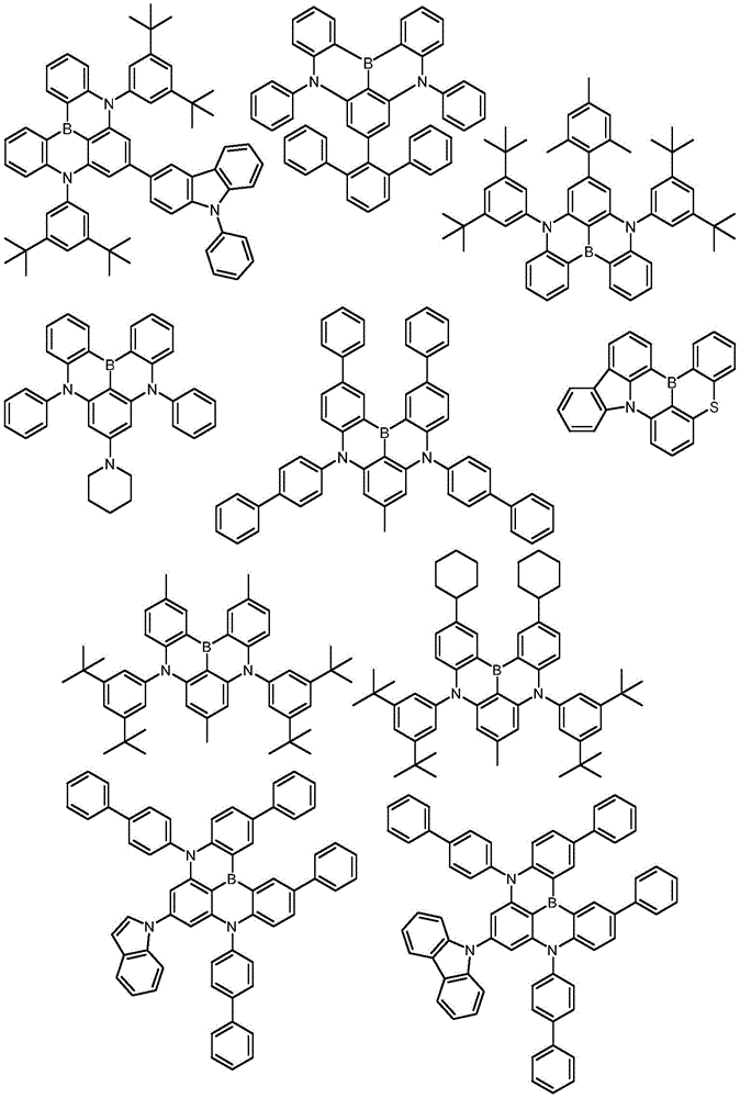
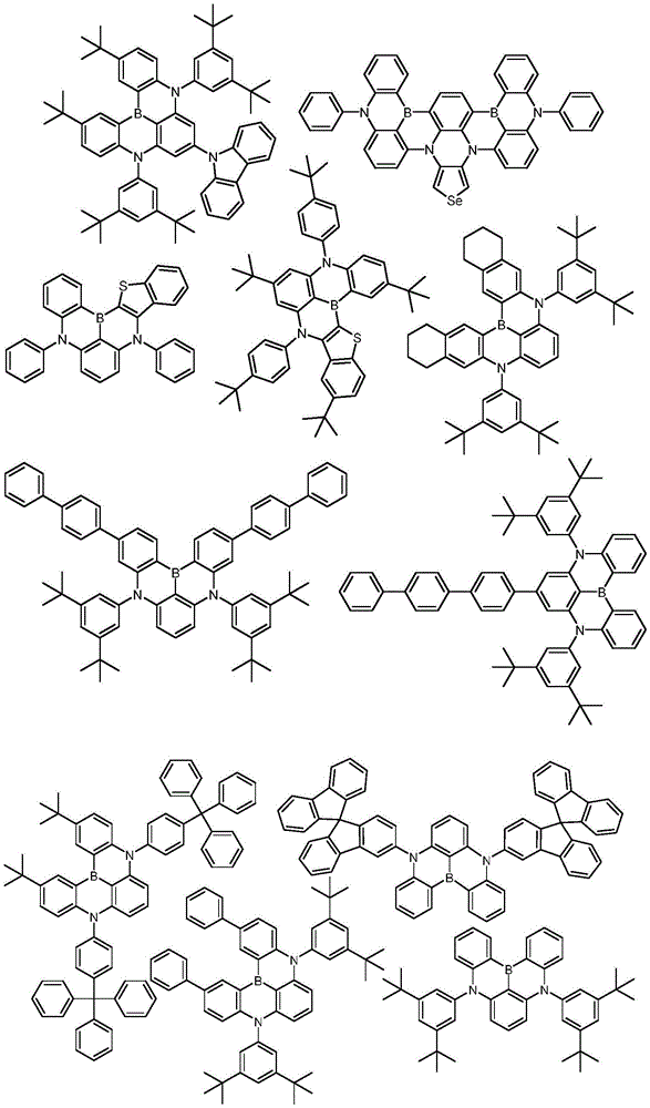
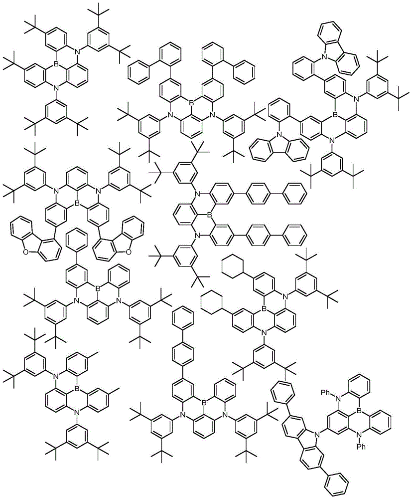
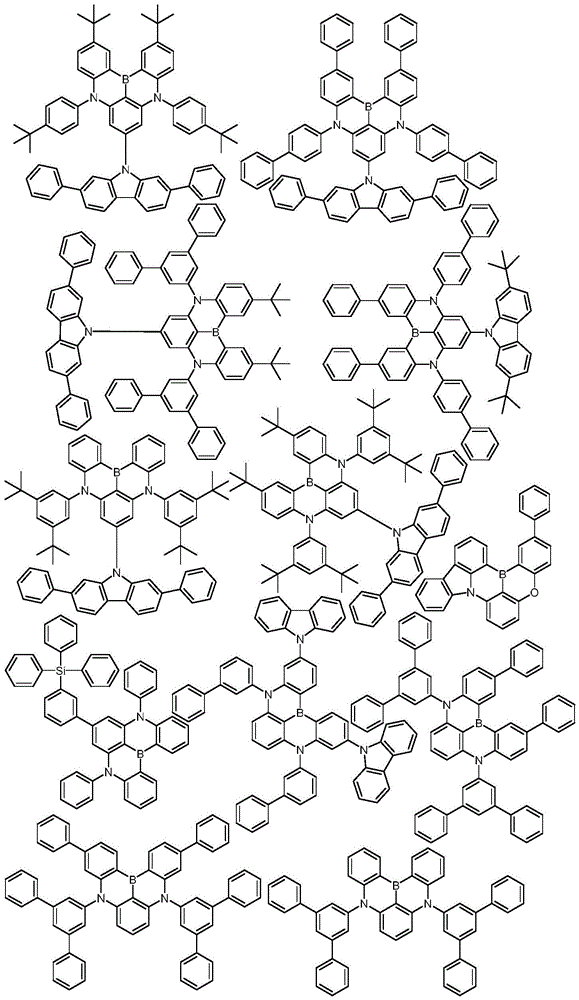
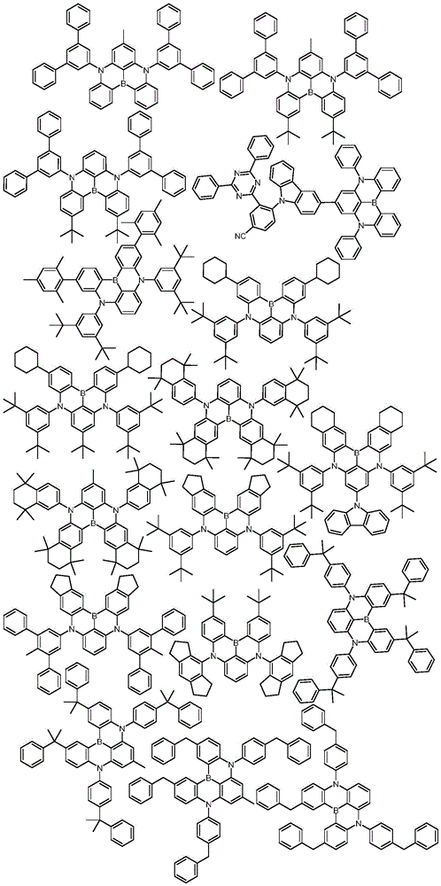
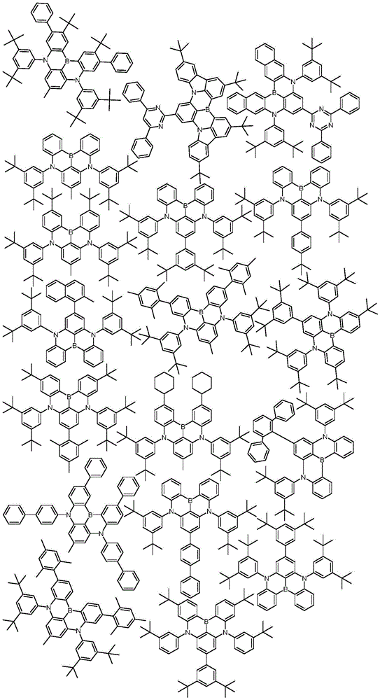

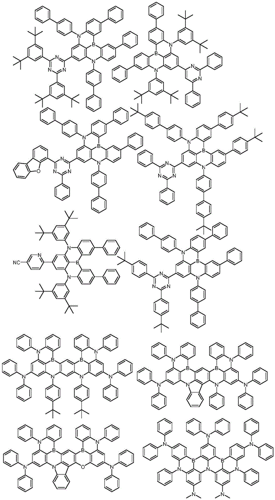
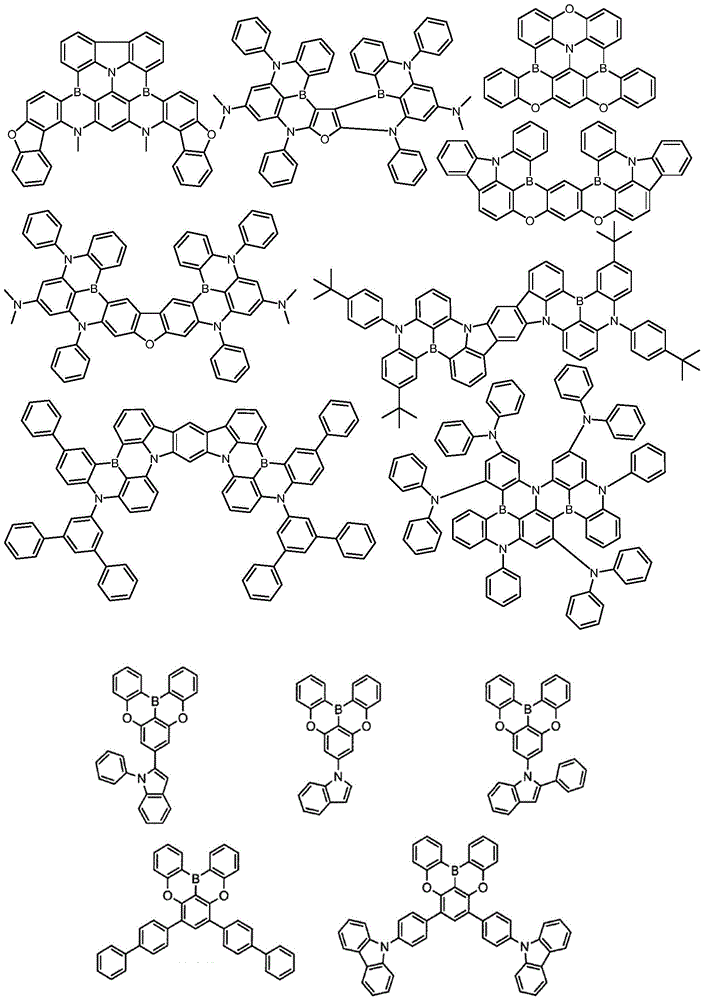


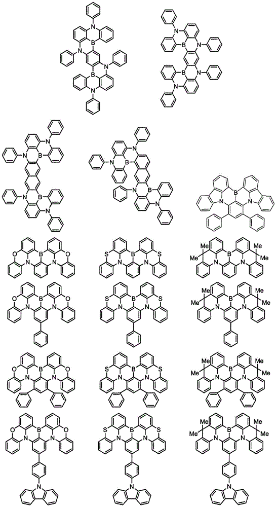


Small FWHM emitters S which can be used in the context of the invention B Is a emitter comprising or consisting of a structure according to the formula BNE-1 below:

wherein,,
c and d are both integers and are independently selected from 0 and 1;
e and f are both integers and are selected from 0 and 1, wherein e and f are (always) the same (i.e., both are 0 or both are 1);
g and h are both integers and are selected from 0 and 1, wherein g and h are (always) the same (i.e., both are 0 or both are 1);
if d is 0, both e and f are 1, and if d is 1, both e and f are 0;
if c is 0, then both g and h are 1, if c is 1, then both g and h are 0;
V 1 selected from nitrogen (N) and CR BNE-V ;
V 2 Selected from nitrogen (N) and CR BNE-I ;
X 3 Is selected from the group consisting of direct bond, CR BNE-3 R BNE-4 、C=CR BNE-3 R BNE-4 、C=O、C=NR BNE-3 、NR BNE-3 、O、SiR BNE -3 R BNE-4 S, S (O) and S (O) 2 A group of;
Y 2 is selected from the group consisting of direct bond, CR BNE-3′ R BNE-4′ 、C=CR BNE-3′ R BNE-4′ 、C=O、C=NR BNE-3′ 、NR BNE-3′ 、O、SiR BNE-3′ R BNE-4′ S, S (O) and S (O) 2 A group of;
R BNE-1 、R BNE-2 、R BNE-1′ 、R BNE-2′ 、R BNE-3 、R BNE-4 、R BNE-3′ 、R BNE-4′ 、R BNE-I 、R BNE-II 、R BNE-III 、R BNE-IV and R is BNE-V Are each independently selected from the group consisting of: hydrogen; deuterium; n (R) BNE-5 ) 2 ;OR BNE-5 ;Si(R BNE-5 ) 3 ;B(OR BNE -5 ) 2 ;B(R BNE-5 ) 2 ;OSO 2 R BNE-5 ;CF 3 ;CN;F;Cl;Br;I;C 1 -C 40 Alkyl optionally substituted with one or more substituents R BNE-5 And wherein one or more non-adjacent CH' s 2 The radicals being optionally substituted by R BNE-5 C=CR BNE-5 、C≡C、Si(R BNE -5 ) 2 、Ge(R BNE-5 ) 2 、Sn(R BNE-5 ) 2 、C=O、C=S、C=Se、C=NR BNE-5 、P(=O)(R BNE-5 )、SO、SO 2 、NR BNE-5 O, S or CONR BNE-5 Substitution; c (C) 1 -C 40 Alkoxy optionally substituted with one or more substituents R BNE-5 And wherein one or more non-adjacent CH' s 2 The radicals being optionally substituted by R BNE-5 C=CR BNE-5 、C≡C、Si(R BNE-5 ) 2 、Ge(R BNE-5 ) 2 、Sn(R BNE-5 ) 2 、C=O、C=S、C=Se、C=NR BNE-5 、P(=O)(R BNE-5 )、SO、SO 2 、NR BNE-5 O, S or CONR BNE-5 Substitution; c (C) 1 -C 40 Thioalkoxy optionally substituted with one or more substituents R BNE-5 And wherein one or more non-adjacent CH' s 2 The radicals being optionally substituted by R BNE-5 C=CR BNE-5 、C≡C、Si(R BNE-5 ) 2 、Ge(R BNE-5 ) 2 、Sn(R BNE-5 ) 2 、C=O、C=S、C=Se、C=NR BNE-5 、P(=O)(R BNE-5 )、SO、SO 2 、NR BNE-5 O, S or CONR BNE-5 Substitution; c (C) 2 -C 40 Alkenyl optionally substituted with one or more substituents R BNE-5 And wherein one or more non-adjacent CH' s 2 The radicals being optionally substituted by R BNE-5 C=CR BNE-5 、C≡C、Si(R BNE-5 ) 2 、Ge(R BNE-5 ) 2 、Sn(R BNE-5 ) 2 、C=O、C=S、C=Se、C=NR BNE-5 、P(=O)(R BNE-5 )、SO、SO 2 、NR BNE-5 O, S or CONR BNE-5 Substitution; c (C) 2 -C 40 Alkynyl, optionally substituted with one or more substituents R BNE-5 And wherein one or more non-adjacent CH' s 2 The radicals being optionally substituted by R BNE-5 C=CR BNE-5 、Si(R BNE-5 ) 2 、Ge(R BNE-5 ) 2 、Sn(R BNE-5 ) 2 、C=O、C=S、C=Se、C=NR BNE-5 、P(=O)(R BNE-5 )、SO、SO 2 、NR BNE-5 O, S or CONR BNE-5 Substitution; c (C) 6 -C 60 Aryl optionally substituted with one or more substituents R BNE-5 The method comprises the steps of carrying out a first treatment on the surface of the C 2 -C 57 Heteroaryl, optionally substituted with one or more substituents R BNE-5 ;
R BNE-d 、R BNE-d′ And R is BNE-e Independently of each other selected from the group consisting of: hydrogen; deuterium; n (R) BNE-5 ) 2 ;OR BNE-5 ;Si(R BNE-5 ) 3 ;B(OR BNE-5 ) 2 ;B(R BNE-5 ) 2 ;OSO 2 R BNE-5 ;CF 3 ;CN;F;Cl;Br;I;C 1 -C 40 Alkyl optionally substituted with one or more substituents R BNE-a And wherein one or more non-adjacent CH' s 2 The radicals being optionally substituted by R BNE-5 C=CR BNE-5 、C≡C、Si(R BNE-5 ) 2 、Ge(R BNE-5 ) 2 、Sn(R BNE-5 ) 2 、C=O、C=S、C=Se、C=NR BNE-5 、P(=O)(R BNE -5 )、SO、SO 2 、NR BNE-5 O, S or CONR BNE-5 Substitution; c (C) 1 -C 40 Alkoxy optionally substituted with one or more substituents R BNE-a And wherein one or more non-adjacent CH' s 2 The radicals being optionally substituted by R BNE-5 C=CR BNE-5 、C≡C、Si(R BNE-5 ) 2 、Ge(R BNE-5 ) 2 、Sn(R BNE-5 ) 2 、C=O、C=S、C=Se、C=NR BNE-5 、P(=O)(R BNE-5 )、SO、SO 2 、NR BNE-5 O, S or CONR BNE-5 Substitution; c (C) 1 -C 40 Thioalkoxy optionally substituted with one or more substituents R BNE-a And wherein one or more non-adjacent CH' s 2 The radicals being optionally substituted by R BNE-5 C=CR BNE-5 、C≡C、Si(R BNE-5 ) 2 、Ge(R BNE-5 ) 2 、Sn(R BNE -5 ) 2 、C=O、C=S、C=Se、C=NR BNE-5 、P(=O)(R BNE-5 )、SO、SO 2 、NR BNE-5 O, S or CONR BNE-5 Substitution; c (C) 2 -C 40 Alkenyl optionally substituted with one or more substituents R BNE-a And wherein one or more non-adjacent CH' s 2 The radicals being optionally substituted by R BNE-5 C=CR BNE-5 、C≡C、Si(R BNE-5 ) 2 、Ge(R BNE-5 ) 2 、Sn(R BNE-5 ) 2 、C=O、C=S、C=Se、C=NR BNE-5 、P(=O)(R BNE-5 )、SO、SO 2 、NR BNE-5 O, S or CONR BNE-5 Substitution; c (C) 2 -C 40 Alkynyl, optionally substituted with one or more substituents R BNE-a And wherein one or more non-adjacent CH' s 2 The radicals being optionally substituted by R BNE-5 C=CR BNE -5 、Si(R BNE-5 ) 2 、Ge(R BNE-5 ) 2 、Sn(R BNE-5 ) 2 、C=O、C=S、C=Se、C=NR BNE-5 、P(=O)(R BNE-5 )、SO、SO 2 、NR BNE-5 O, S or CONR BNE-5 Substitution; c (C) 6 -C 60 Aryl optionally substituted with one or more substituents R BNE-a The method comprises the steps of carrying out a first treatment on the surface of the C 2 -C 57 Heteroaryl, optionally substituted with one or more substituents R BNE-a ;
R BNE-a Independently of each other at each occurrence selected from the group consisting of: hydrogen; deuterium; n (R) BNE-5 ) 2 ;OR BNE-5 ;Si(R BNE-5 ) 3 ;B(OR BNE-5 ) 2 ;B(R BNE-5 ) 2 ;OSO 2 R BNE-5 ;CF 3 ;CN;F;Cl;Br;I;C 1 -C 40 Alkyl optionally substituted with one or more substituents R BNE-5 And wherein one or more non-adjacent CH' s 2 The radicals being optionally substituted by R BNE-5 C=CR BNE-5 、C≡C、Si(R BNE-5 ) 2 、Ge(R BNE-5 ) 2 、Sn(R BNE-5 ) 2 、C=O、C=S、C=Se、C=NR BNE-5 、P(=O)(R BNE -5 )、SO、SO 2 、NR BNE-5 O, S or CONR BNE-5 Substitution; c (C) 1 -C 40 Alkoxy optionally substituted with one or more substituents R BNE-5 And wherein one or more non-adjacent CH' s 2 The radicals being optionally substituted by R BNE-5 C=CR BNE-5 、C≡C、Si(R BNE-5 ) 2 、Ge(R BNE-5 ) 2 、Sn(R BNE-5 ) 2 、C=O、C=S、C=Se、C=NR BNE-5 、P(=O)(R BNE-5 )、SO、SO 2 、NR BNE-5 O, S or CONR BNE-5 Substitution; c (C) 1 -C 40 Thioalkoxy optionally substituted with one or more substituents R BNE-5 And wherein one or more non-adjacent CH' s 2 The radicals being optionally substituted by R BNE-5 C=CR BNE-5 、C≡C、Si(R BNE-5 ) 2 、Ge(R BNE-5 ) 2 、Sn(R BNE -5 ) 2 、C=O、C=S、C=Se、C=NR BNE-5 、P(=O)(R BNE-5 )、SO、SO 2 、NR BNE-5 O, S or CONR BNE-5 Substitution; c (C) 2 -C 40 Alkenyl optionally substituted with one or more substituents R BNE-5 And wherein one or more non-adjacent CH' s 2 The radicals being optionally substituted by R BNE-5 C=CR BNE-5 、C≡C、Si(R BNE-5 ) 2 、Ge(R BNE-5 ) 2 、Sn(R BNE-5 ) 2 、C=O、C=S、C=Se、C=NR BNE-5 、P(=O)(R BNE-5 )、SO、SO 2 、NR BNE-5 O, S or CONR BNE-5 Substitution; c (C) 2 -C 40 Alkynyl, optionally substituted with one or more substituents R BNE-5 And wherein one or more non-adjacent CH' s 2 The radicals being optionally substituted by R BNE-5 C=CR BNE -5 、Si(R BNE-5 ) 2 、Ge(R BNE-5 ) 2 、Sn(R BNE-5 ) 2 、C=O、C=S、C=Se、C=NR BNE-5 、P(=O)(R BNE-5 )、SO、SO 2 、NR BNE-5 O, S or CONR BNE-5 Substitution; c (C) 6 -C 60 Aryl optionally substituted with one or more substituents R BNE-5 The method comprises the steps of carrying out a first treatment on the surface of the C 2 -C 57 Heteroaryl, optionally substituted with one or more substituents R BNE-5 ;
R BNE-5 Independently of each other at each occurrence selected from the group consisting of: hydrogen; deuterium; n (R) BNE-6 ) 2 ;OR BNE-6 ;Si(R BNE-6 ) 3 ;B(OR BNE-6 ) 2 ;B(R BNE-6 ) 2 ;OSO 2 R BNE-6 ;CF 3 ;CN;F;Cl;Br;I;C 1 -C 40 Alkyl optionally substituted with one or more substituents R BNE-6 And wherein one or more non-adjacent CH' s 2 The radicals being optionally substituted by R BNE-6 C=CR BNE-6 、C≡C、Si(R BNE-6 ) 2 、Ge(R BNE-6 ) 2 、Sn(R BNE-6 ) 2 、C=O、C=S、C=Se、C=NR BNE-6 、P(=O)(R BNE -6 )、SO、SO 2 、NR BNE-6 O, S or CONR BNE-6 Substitution; c (C) 1 -C 40 Alkoxy optionally substituted with one or more substituents R BNE-6 And wherein one or more non-adjacent CH' s 2 The radicals being optionally substituted by R BNE-6 C=CR BNE-6 、C≡C、Si(R BNE-6 ) 2 、Ge(R BNE-6 ) 2 、Sn(R BNE-6 ) 2 、C=O、C=S、C=Se、C=NR BNE-6 、P(=O)(R BNE-6 )、SO、SO 2 、NR BNE-6 O, S or CONR BNE-6 Substitution; c (C) 1 -C 40 Thioalkoxy optionally substituted with one or more substituents R BNE-6 And wherein one or more non-adjacent CH' s 2 The radicals being optionally substituted by R BNE-6 C=CR BNE-6 、C≡C、Si(R BNE-6 ) 2 、Ge(R BNE-6 ) 2 、Sn(R BNE -6 ) 2 、C=O、C=S、C=Se、C=NR BNE-6 、P(=O)(R BNE-6 )、SO、SO 2 、NR BNE-6 O, S or CONR BNE-6 Substitution; c (C) 2 -C 40 Alkenyl optionally substituted with one or more substituents R BNE-6 And wherein one or more non-adjacent CH' s 2 The radicals being optionally substituted by R BNE-6 C=CR BNE-6 、C≡C、Si(R BNE-6 ) 2 、Ge(R BNE-6 ) 2 、Sn(R BNE-6 ) 2 、C=O、C=S、C=Se、C=NR BNE-6 、P(=O)(R BNE-6 )、SO、SO 2 、NR BNE-6 O, S or CONR BNE-6 Substitution; c (C) 2 -C 40 Alkynyl, optionally substituted with one or more substituents R BNE-6 And wherein one or more non-adjacent CH' s 2 The radicals being optionally substituted by R BNE-6 C=CR BNE -6 、Si(R BNE-6 ) 2 、Ge(R BNE-6 ) 2 、Sn(R BNE-6 ) 2 、C=O、C=S、C=Se、C=NR BNE-6 、P(=O)(R BNE-6 )、SO、SO 2 、NR BNE-6 O, S or CONR BNE-6 Substitution; c (C) 6 -C 60 Aryl optionally substituted with one or more substituents R BNE-6 The method comprises the steps of carrying out a first treatment on the surface of the C 2 -C 57 Heteroaryl, optionally substituted with one or more substituents R BNE-6 ;
R BNE-6 Independently at each occurrence selected from the group consisting ofAnd (3) a group consisting of: hydrogen; deuterium; OPh; CF (compact flash) 3 ;CN;F;C 1 -C 5 Alkyl, wherein one or more hydrogen atoms are optionally replaced by deuterium, CN, CF independently of one another 3 Substitution by Ph or F; c (C) 1 -C 5 Alkoxy, wherein one or more hydrogen atoms are optionally replaced by deuterium, CN, CF independently of one another 3 Or F substitution; c (C) 1 -C 5 Thioalkoxy groups in which one or more hydrogen atoms are optionally replaced by deuterium, CN, CF independently of one another 3 Or F substitution; c (C) 2 -C 5 Alkenyl in which one or more hydrogen atoms are optionally replaced independently of one another by deuterium, CN, CF 3 Or F substitution; c (C) 2 -C 5 Alkynyl, wherein one or more hydrogen atoms are optionally replaced independently of each other by deuterium, CN, CF 3 Or F substitution; c (C) 6 -C 18 Aryl optionally substituted with one or more C 1 -C 5 An alkyl substituent; c (C) 2 -C 17 Heteroaryl, optionally substituted with one or more C 1 -C 5 An alkyl substituent; n (C) 6 -C 18 Aryl group 2 ;N(C 2 -C 17 Heteroaryl group 2 The method comprises the steps of carrying out a first treatment on the surface of the N (C) 2 -C 17 Heteroaryl) (C) 6 -C 18 An aryl group);
wherein R is BNE-III And R is BNE-e Optionally combining to form a direct single bond; and is also provided with
Wherein the substituents R BNE-a 、R BNE-d 、R BNE-d′ 、R BNE-e 、R BNE-3′ 、R BNE-4′ And R is BNE-5 Optionally forming a mono-or polycyclic aliphatic or aromatic or heteroaromatic carbocyclic or heterocyclic ring system with each other;
wherein the substituents R BNE-1 、R BNE-2 、R BNE-1′ 、R BNE-2′ 、R BNE-3 、R BNE-4 、R BNE-5 、R BNE-I 、R BNE-II 、R BNE-III 、R BNE-IV And R is BNE-V Optionally forming a mono-or polycyclic aliphatic or aromatic or heteroaromatic group with one anotherA carbocyclic or heterocyclic ring system of (c);
wherein optionally two or more (preferably two) structures of formula BNE-1 are conjugated to each other (preferably fused to each other by sharing at least one (more preferably exactly one) bond);
wherein optionally two or more (preferably two) structures of formula BNE-1 are present in the emitter and share at least one (preferably exactly one) aromatic or heteroaromatic ring (i.e. which may be part of both structures of formula BNE-1), which is preferably any one of rings a, b and c' of formula BNE-1, but may also be selected from R BNE-1 、R BNE-2 、R BNE-1′ 、R BNE-2′ 、R BNE-3 、R BNE-4 、R BNE-3′ 、R BNE-4′ 、R BNE-5 、R BNE-6 、R BNE-I 、R BNE-II 、R BNE-III 、R BNE-IV 、R BNE-V 、R BNE-a 、R BNE-e 、R BNE-d And R is BNE-d′ Or any aromatic or heteroaromatic ring formed from two or more substituents as described above, wherein the shared ring may constitute the same or different parts of two or more structures of formula BNE-1 that share a ring (i.e., the shared ring may be, for example, ring c 'of two structures of formula BNE-1 optionally included in the emitter, or the shared ring may be, for example, ring b of one structure and ring c') of another structure of formula BNE-1 optionally included in the emitter); and is also provided with
Wherein, optionally, R BNE-1 、R BNE-2 、R BNE-1′ 、R BNE-2′ 、R BNE-3 、R BNE-4 、R BNE-5 、R BNE-3′ 、R BNE-4′ 、R BNE-6 、R BNE-I 、R BNE-II 、R BNE-III 、R BNE-IV 、R BNE-V 、R BNE-a 、R BNE-e 、R BNE-d And R is BNE-d′ Is replaced by a bond to a further chemical entity of formula BNE-1And/or wherein, optionally, R BNE-1 、R BNE-2 、R BNE-1′ 、R BNE-2′ 、R BNE-3 、R BNE -4 、R BNE-5 、R BNE-3′ 、R BNE-4′ 、R BNE-6 、R BNE-I 、R BNE-II 、R BNE-III 、R BNE-IV 、R BNE-V 、R BNE-a 、R BNE-e 、R BNE-d And R is BNE-d′ At least one hydrogen atom of any of them is replaced by a bond to a further chemical entity of formula BNE-1.
In one embodiment of the invention, in the light emitting layer B, a small FWHM emitter S B Including structures according to formula BNE-1.
In one embodiment of the invention, a small FWHM emitter S B Comprising or consisting of a structure according to formula BNE-1, V 1 Is CR (CR) BNE-V And V is 2 Is CR (CR) BNE-I 。
In one embodiment of the invention, a small FWHM emitter S B Comprising or consisting of a structure according to formula BNE-1, V 1 And V 2 Both are nitrogen (N).
In one embodiment of the invention, a small FWHM emitter S B Comprising or consisting of a structure according to formula BNE-1, V 1 Is nitrogen (N), and V 2 Is CR (CR) BNE-I 。
In one embodiment of the invention, a small FWHM emitter S B Comprising or consisting of a structure according to formula BNE-1, V 1 Is CR (CR) BNE-V And V is 2 Is nitrogen (N).
In one embodiment of the invention, a small FWHM emitter S B Comprising or consisting of a structure according to formula BNE-1, both c and d being 0.
In one embodiment of the invention, a small FWHM emitter S B Comprising or consisting of a structure according to formula BNE-1, c is 0 and d is 1.
In one embodiment of the inventionMedium, small FWHM emitter S B Comprising or consisting of a structure according to formula BNE-1, c is 1 and d is 0.
In one embodiment of the invention, a small FWHM emitter S B Comprising or consisting of a structure according to formula BNE-1, both c and d being 1.
In one embodiment of the invention, a small FWHM emitter S B Comprising or consisting of a structure according to formula BNE-1,
X 3 Is selected from the group consisting of direct bond, CR BNE-3 R BNE-4 、C=O、NR BNE-3 O, S and SiR BNE-3 R BNE-4 A group of; and is also provided with
Y 2 Is selected from the group consisting of direct bond, CR BNE-3′ R BNE-4′ 、C=O、NR BNE-3′ O, S and SiR BNE-3′ R BNE-4′ A group of groups.
In one embodiment of the invention, a small FWHM emitter S B Comprising or consisting of a structure according to formula BNE-1,
X 3 is selected from the group consisting of direct bond, CR BNE-3 R BNE-4 、NR BNE-3 O, S and SiR BNE-3 R BNE-4 A group of; and is also provided with
Y 2 Is selected from the group consisting of direct bond, CR BNE-3′ R BNE-4′ 、NR BNE-3′ O, S and SiR BNE-3′ R BNE-4′ A group of groups.
In one embodiment of the invention, wherein in at least one (preferably each) light emitting layer B, one or more small FWHM emitters S B At least one (preferably each) of which comprises or consists of a structure according to formula BNE-1,
X 3 is selected from the group consisting of direct bond, CR BNE-3 R BNE-4 、NR BNE-3 O, S and SiR BNE-3 R BNE-4 A group of; and is also provided with
Y 2 Is a direct bond.
In one of the inventionsIn an embodiment, a small FWHM emitter S B Comprising or consisting of a structure according to formula BNE-1,
X 3 is a direct bond or NR BNE-3 The method comprises the steps of carrying out a first treatment on the surface of the And is also provided with
Y 2 Is a direct bond.
In one embodiment of the invention, a small FWHM emitter S B Comprising or consisting of a structure according to formula BNE-1,
X 3 is NR BNE-3 The method comprises the steps of carrying out a first treatment on the surface of the And is also provided with
Y 2 Is a direct bond.
In one embodiment of the invention, a small FWHM emitter S B Comprising or consisting of a structure according to formula BNE-1,
R BNE-1 、R BNE-2 、R BNE-1′ 、R BNE-2′ 、R BNE-3 、R BNE-4 、R BNE-3′ 、R BNE-4′ 、R BNE-I 、R BNE-II 、R BNE-III 、R BNE-IV and R is BNE-V Are each independently selected from the group consisting of: hydrogen; deuterium; n (R) BNE-5 ) 2 ;OR BNE-5 ;Si(R BNE-5 ) 3 ;B(OR BNE -5 ) 2 ;B(R BNE-5 ) 2 ;OSO 2 R BNE-5 ;CF 3 ;CN;F;Cl;Br;I;C 1 -C 40 Alkyl optionally substituted with one or more substituents R BNE-5 And wherein one or more non-adjacent CH' s 2 The radicals being optionally substituted by R BNE-5 C=CR BNE-5 、C≡C、Si(R BNE -5 ) 2 、Ge(R BNE-5 ) 2 、Sn(R BNE-5 ) 2 、C=O、C=S、C=Se、C=NR BNE-5 、P(=O)(R BNE-5 )、SO、SO 2 、NR BNE-5 O, S or CONR BNE-5 Substitution; c (C) 1 -C 40 Alkoxy optionally substituted with one or more substituents R BNE-5 And wherein one or more non-adjacent CH' s 2 The radicals being optionally coveredR BNE-5 C=CR BNE-5 、C≡C、Si(R BNE-5 ) 2 、Ge(R BNE-5 ) 2 、Sn(R BNE-5 ) 2 、C=O、C=S、C=Se、C=NR BNE-5 、P(=O)(R BNE-5 )、SO、SO 2 、NR BNE-5 O, S or CONR BNE-5 Substitution; c (C) 1 -C 40 Thioalkoxy optionally substituted with one or more substituents R BNE-5 And wherein one or more non-adjacent CH' s 2 The radicals being optionally substituted by R BNE-5 C=CR BNE-5 、C≡C、Si(R BNE-5 ) 2 、Ge(R BNE-5 ) 2 、Sn(R BNE-5 ) 2 、C=O、C=S、C=Se、C=NR BNE-5 、P(=O)(R BNE-5 )、SO、SO 2 、NR BNE-5 O, S or CONR BNE-5 Substitution; c (C) 2 -C 40 Alkenyl optionally substituted with one or more substituents R BNE-5 And wherein one or more non-adjacent CH' s 2 The radicals being optionally substituted by R BNE-5 C=CR BNE-5 、C≡C、Si(R BNE-5 ) 2 、Ge(R BNE-5 ) 2 、Sn(R BNE-5 ) 2 、C=O、C=S、C=Se、C=NR BNE-5 、P(=O)(R BNE-5 )、SO、SO 2 、NR BNE-5 O, S or CONR BNE-5 Substitution; c (C) 2 -C 40 Alkynyl, optionally substituted with one or more substituents R BNE-5 And wherein one or more non-adjacent CH' s 2 The radicals being optionally substituted by R BNE-5 C=CR BNE-5 、Si(R BNE-5 ) 2 、Ge(R BNE-5 ) 2 、Sn(R BNE-5 ) 2 、C=O、C=S、C=Se、C=NR BNE-5 、P(=O)(R BNE-5 )、SO、SO 2 、NR BNE-5 O, S or CONR BNE-5 Substitution; c (C) 6 -C 60 Aryl optionally substituted with one or more substituents R BNE-5 The method comprises the steps of carrying out a first treatment on the surface of the C 2 -C 57 Heteroaryl, optionally substituted with one or more substituents R BNE-5 ;
R BNE-d 、R BNE-d′ And R is BNE-e Independently of each other selected from the group consisting of: hydrogen; deuterium; CF (compact flash) 3 ;CN;F;Cl;Br;I;C 1 -C 40 Alkyl optionally substituted with one or more substituents R BNE-a And wherein one or more non-adjacent CH' s 2 The radicals being optionally substituted by R BNE-5 C=CR BNE-5 、C≡C、Si(R BNE-5 ) 2 、Ge(R BNE-5 ) 2 、Sn(R BNE-5 ) 2 、C=O、C=S、C=Se、C=NR BNE-5 、P(=O)(R BNE-5 )、SO、SO 2 、NR BNE-5 O, S or CONR BNE-5 Substitution; c (C) 6 -C 60 Aryl optionally substituted with one or more substituents R BNE-a The method comprises the steps of carrying out a first treatment on the surface of the C 2 -C 57 Heteroaryl, optionally substituted with one or more substituents R BNE-a ;
R BNE-a Independently of each other at each occurrence selected from the group consisting of: hydrogen; deuterium; n (R) BNE-5 ) 2 ;OR BNE-5 ;Si(R BNE-5 ) 3 ;B(OR BNE-5 ) 2 ;B(R BNE-5 ) 2 ;OSO 2 R BNE-5 ;CF 3 ;CN;F;Cl;Br;I;C 1 -C 40 Alkyl optionally substituted with one or more substituents R BNE-5 And wherein one or more non-adjacent CH' s 2 The radicals being optionally substituted by R BNE-5 C=CR BNE-5 、C≡C、Si(R BNE-5 ) 2 、Ge(R BNE-5 ) 2 、Sn(R BNE-5 ) 2 、C=O、C=S、C=Se、C=NR BNE-5 、P(=O)(R BNE -5 )、SO、SO 2 、NR BNE-5 O, S or CONR BNE-5 Substitution; c (C) 1 -C 40 Alkoxy optionally substituted with one or more substituents R BNE-5 And wherein one or more non-adjacent CH' s 2 The radicals being optionally substituted by R BNE-5 C=CR BNE-5 、C≡C、Si(R BNE-5 ) 2 、Ge(R BNE-5 ) 2 、Sn(R BNE-5 ) 2 、C=O、C=S、C=Se、C=NR BNE-5 、P(=O)(R BNE-5 )、SO、SO 2 、NR BNE-5 O, S or CONR BNE-5 Substitution; c (C) 1 -C 40 Thioalkoxy optionally substituted with one or more substituents R BNE-5 And wherein one or more non-adjacent CH' s 2 The radicals being optionally substituted by R BNE-5 C=CR BNE-5 、C≡C、Si(R BNE-5 ) 2 、Ge(R BNE-5 ) 2 、Sn(R BNE -5 ) 2 、C=O、C=S、C=Se、C=NR BNE-5 、P(=O)(R BNE-5 )、SO、SO 2 、NR BNE-5 O, S or CONR BNE-5 Substitution; c (C) 2 -C 40 Alkenyl optionally substituted with one or more substituents R BNE-5 And wherein one or more non-adjacent CH' s 2 The radicals being optionally substituted by R BNE-5 C=CR BNE-5 、C≡C、Si(R BNE-5 ) 2 、Ge(R BNE-5 ) 2 、Sn(R BNE-5 ) 2 、C=O、C=S、C=Se、C=NR BNE-5 、P(=O)(R BNE-5 )、SO、SO 2 、NR BNE-5 O, S or CONR BNE-5 Substitution; c (C) 2 -C 40 Alkynyl, optionally substituted with one or more substituents R BNE-5 And wherein one or more non-adjacent CH' s 2 The radicals being optionally substituted by R BNE-5 C=CR BNE -5 、Si(R BNE-5 ) 2 、Ge(R BNE-5 ) 2 、Sn(R BNE-5 ) 2 、C=O、C=S、C=Se、C=NR BNE-5 、P(=O)(R BNE-5 )、SO、SO 2 、NR BNE-5 O, S or CONR BNE-5 Substitution; c (C) 6 -C 60 Aryl optionally substituted with one or more substituents R BNE-5 The method comprises the steps of carrying out a first treatment on the surface of the C 2 -C 57 Heteroaryl, optionally substituted with one or more substituents R BNE-5 ;
R BNE-5 Independently of each other at each occurrence selected from the group consisting of: hydrogen gasThe method comprises the steps of carrying out a first treatment on the surface of the Deuterium; n (R) BNE-6 ) 2 ;OR BNE-6 ;Si(R BNE-6 ) 3 ;B(OR BNE-6 ) 2 ;B(R BNE-6 ) 2 ;OSO 2 R BNE-6 ;CF 3 ;CN;F;Cl;Br;I;C 1 -C 40 Alkyl optionally substituted with one or more substituents R BNE-6 And wherein one or more non-adjacent CH' s 2 The radicals being optionally substituted by R BNE-6 C=CR BNE-6 、C≡C、Si(R BNE-6 ) 2 、Ge(R BNE-6 ) 2 、Sn(R BNE-6 ) 2 、C=O、C=S、C=Se、C=NR BNE-6 、P(=O)(R BNE -6 )、SO、SO 2 、NR BNE-6 O, S or CONR BNE-6 Substitution; c (C) 1 -C 40 Alkoxy optionally substituted with one or more substituents R BNE-6 And wherein one or more non-adjacent CH' s 2 The radicals being optionally substituted by R BNE-6 C=CR BNE-6 、C≡C、Si(R BNE-6 ) 2 、Ge(R BNE-6 ) 2 、Sn(R BNE-6 ) 2 、C=O、C=S、C=Se、C=NR BNE-6 、P(=O)(R BNE-6 )、SO、SO 2 、NR BNE-6 O, S or CONR BNE-6 Substitution; c (C) 1 -C 40 Thioalkoxy optionally substituted with one or more substituents R BNE-6 And wherein one or more non-adjacent CH' s 2 The radicals being optionally substituted by R BNE-6 C=CR BNE-6 、C≡C、Si(R BNE-6 ) 2 、Ge(R BNE-6 ) 2 、Sn(R BNE -6 ) 2 、C=O、C=S、C=Se、C=NR BNE-6 、P(=O)(R BNE-6 )、SO、SO 2 、NR BNE-6 O, S or CONR BNE-6 Substitution; c (C) 2 -C 40 Alkenyl optionally substituted with one or more substituents R BNE-6 And wherein one or more non-adjacent CH' s 2 The radicals being optionally substituted by R BNE-6 C=CR BNE-6 、C≡C、Si(R BNE-6 ) 2 、Ge(R BNE-6 ) 2 、Sn(R BNE-6 ) 2 、C=O、C=S、C=Se、C=NR BNE-6 、P(=O)(R BNE-6 )、SO、SO 2 、NR BNE-6 O, S or CONR BNE-6 Substitution; c (C) 2 -C 40 Alkynyl, optionally substituted with one or more substituents R BNE-6 And wherein one or more non-adjacent CH' s 2 The radicals being optionally substituted by R BNE-6 C=CR BNE -6 、Si(R BNE-6 ) 2 、Ge(R BNE-6 ) 2 、Sn(R BNE-6 ) 2 、C=O、C=S、C=Se、C=NR BNE-6 、P(=O)(R BNE-6 )、SO、SO 2 、NR BNE-6 O, S or CONR BNE-6 Substitution; c (C) 6 -C 60 Aryl optionally substituted with one or more substituents R BNE-6 The method comprises the steps of carrying out a first treatment on the surface of the C 2 -C 57 Heteroaryl, optionally substituted with one or more substituents R BNE-6 ;
R BNE-6 Independently of each other at each occurrence selected from the group consisting of: hydrogen; deuterium; OPh; CF (compact flash) 3 ;CN;F;C 1 -C 5 Alkyl, wherein one or more hydrogen atoms are optionally replaced by deuterium, CN, CF independently of one another 3 Substitution by Ph or F; c (C) 1 -C 5 Alkoxy, wherein one or more hydrogen atoms are optionally replaced by deuterium, CN, CF independently of one another 3 Or F substitution; c (C) 1 -C 5 Thioalkoxy groups in which one or more hydrogen atoms are optionally replaced by deuterium, CN, CF independently of one another 3 Or F substitution; c (C) 2 -C 5 Alkenyl in which one or more hydrogen atoms are optionally replaced independently of one another by deuterium, CN, CF 3 Or F substitution; c (C) 2 -C 5 Alkynyl, wherein one or more hydrogen atoms are optionally replaced independently of each other by deuterium, CN, CF 3 Or F substitution; c (C) 6 -C 18 Aryl optionally substituted with one or more C 1 -C 5 An alkyl substituent; c (C) 2 -C 17 Heteroaryl, optionally substituted with one or more C 1 -C 5 An alkyl substituent; n (C) 6 -C 18 Aryl group 2 ;N(C 2 -C 17 Heteroaryl group 2 The method comprises the steps of carrying out a first treatment on the surface of the N (C) 2 -C 17 Heteroaryl) (C) 6 -C 18 An aryl group);
Wherein R is BNE-III And R is BNE-e Optionally combining to form a direct single bond; and is also provided with
Wherein the substituents R BNE-a 、R BNE-d 、R BNE-d′ 、R BNE-e 、R BNE-3′ 、R BNE-4′ And R is BNE-5 Optionally forming a mono-or polycyclic aliphatic or aromatic or heteroaromatic carbocyclic or heterocyclic ring system with each other;
wherein the substituents R BNE-1 、R BNE-2 、R BNE-1′ 、R BNE-2′ 、R BNE-3 、R BNE-4 、R BNE-5 、R BNE-I 、R BNE-II 、R BNE-III 、R BNE-IV And R is BNE-V Optionally forming a mono-or polycyclic aliphatic or aromatic or heteroaromatic carbocyclic or heterocyclic ring system with each other;
wherein optionally two or more (preferably two) structures of formula BNE-1 are conjugated to each other (preferably fused to each other by sharing at least one (more preferably exactly one) bond);
wherein optionally two or more (preferably two) structures of formula BNE-1 are present in the emitter and share at least one (preferably exactly one) aromatic or heteroaromatic ring (i.e. which may be part of both structures of formula BNE-1), which is preferably any one of rings a, b and c' of formula BNE-1, but may also be selected from R BNE-1 、R BNE-2 、R BNE-1′ 、R BNE-2′ 、R BNE-3 、R BNE-4 、R BNE-3′ 、R BNE-4′ 、R BNE-5 、R BNE-6 、R BNE-I 、R BNE-II 、R BNE-III 、R BNE-IV 、R BNE-V 、R BNE-a 、R BNE-e 、R BNE-d And R is BNE-d′ Any aromatic or heteroaromatic substituent of (a), or any aromatic or heteroaromatic ring formed from two or more substituents as described above; wherein the shared ring may constitute the same or different parts of two or more structures of the formula BNE-1 of the shared ring (i.e. the shared ring may for example be a ring c 'of two structures of the formula BNE-1 optionally comprised in the emitter, or the shared ring may for example be a ring b of one structure and a ring c') of another structure of the formula BNE-1 optionally comprised in the emitter; and is also provided with
Wherein, optionally, R BNE-1 、R BNE-2 、R BNE-1′ 、R BNE-2′ 、R BNE-3 、R BNE-4 、R BNE-5 、R BNE-3′ 、R BNE-4′ 、R BNE-6 、R BNE-I 、R BNE-II 、R BNE-III 、R BNE-IV 、R BNE-V 、R BNE-a 、R BNE-e 、R BNE-d And R is BNE-d′ Is replaced by a bond to a further chemical entity of formula BNE-1, and/or wherein, optionally, R BNE-1 、R BNE-2 、R BNE-1′ 、R BNE-2′ 、R BNE-3 、R BNE -4 、R BNE-5 、R BNE-3′ 、R BNE-4′ 、R BNE-6 、R BNE-I 、R BNE-II 、R BNE-III 、R BNE-IV 、R BNE-V 、R BNE-a 、R BNE-e 、R BNE-d And R is BNE-d′ At least one hydrogen atom of any of them is replaced by a bond to a further chemical entity of formula BNE-1.
In one embodiment of the invention, a small FWHM emitter S B Comprising or consisting of a structure according to formula BNE-1,
R BNE-1 、R BNE-2 、R BNE-1′ 、R BNE-2′ 、R BNE-3 、R BNE-4 、R BNE-3′ 、R BNE-4′ 、R BNE-I 、R BNE-II 、R BNE-III 、R BNE-IV and R is BNE-V Are each independently selected from the group consisting of: hydrogen; deuterium; n (R) BNE-5 ) 2 ;OR BNE-5 ;Si(R BNE-5 ) 3 ;B(R BNE -5 ) 2 ;CF 3 ;CN;F;Cl;Br;I;C 1 -C 18 Alkyl optionally substituted with one or more substituents R BNE-5 And wherein one or more non-adjacent CH' s 2 The radicals being optionally substituted by R BNE-5 C=CR BNE-5 、C≡C、Si(R BNE-5 ) 2 、Ge(R BNE-5 ) 2 、Sn(R BNE-5 ) 2 、C=O、C=S、C=Se、C=NR BNE-5 、P(=O)(R BNE-5 )、SO、SO 2 、NR BNE-5 O, S or CONR BNE-5 Substitution; c (C) 6 -C 30 Aryl optionally substituted with one or more substituents R BNE-5 The method comprises the steps of carrying out a first treatment on the surface of the C 2 -C 29 Heteroaryl, optionally substituted with one or more substituents R BNE-5 ;
R BNE-d 、R BNE-d′ And R is BNE-e Independently of each other selected from the group consisting of: hydrogen; deuterium; CF (compact flash) 3 ;CN;F;Cl;Br;I;C 1 -C 18 Alkyl optionally substituted with one or more substituents R BNE-a And wherein one or more non-adjacent CH' s 2 The radicals being optionally substituted by R BNE-5 C=CR BNE-5 、C≡C、Si(R BNE-5 ) 2 、Ge(R BNE-5 ) 2 、Sn(R BNE-5 ) 2 、C=O、C=S、C=Se、C=NR BNE-5 、P(=O)(R BNE-5 )、SO、SO 2 、NR BNE-5 O, S or CONR BNE-5 Substitution; c (C) 6 -C 30 Aryl optionally substituted with one or more substituents R BNE-a The method comprises the steps of carrying out a first treatment on the surface of the C 2 -C 29 Heteroaryl, optionally substituted with one or more substituents R BNE-a ;
R BNE-a Independently of each other at each occurrence selected from the group consisting of: hydrogen; deuterium; n (R) BNE-5 ) 2 ;OR BNE-5 ;Si(R BNE-5 ) 3 ;B(R BNE-5 ) 2 ;CF 3 ;CN;F;Cl;Br;I;C 1 -C 18 Alkyl optionally substituted with one or more substituents R BNE-5 And wherein one or more non-adjacent CH' s 2 The radicals being optionally substituted by R BNE-5 C=CR BNE-5 、C≡C、Si(R BNE-5 ) 2 、Ge(R BNE-5 ) 2 、Sn(R BNE-5 ) 2 、C=O、C=S、C=Se、C=NR BNE-5 、P(=O)(R BNE-5 )、SO、SO 2 、NR BNE-5 O, S or CONR BNE-5 Substitution; c (C) 6 -C 30 Aryl optionally substituted with one or more substituents R BNE-5 The method comprises the steps of carrying out a first treatment on the surface of the C 2 -C 29 Heteroaryl, optionally substituted with one or more substituents R BNE-5 ;
R BNE-5 Independently of each other at each occurrence selected from the group consisting of: hydrogen; deuterium; OPh; CF (compact flash) 3 ;CN;F;C 1 -C 5 Alkyl, wherein one or more hydrogen atoms are optionally replaced by deuterium, CN, CF independently of one another 3 Or F substitution; c (C) 1 -C 5 Alkoxy, wherein one or more hydrogen atoms are optionally replaced by deuterium, CN, CF independently of one another 3 Or F substitution; c (C) 1 -C 5 Thioalkoxy groups in which one or more hydrogen atoms are optionally replaced by deuterium, CN, CF independently of one another 3 Or F substitution; c (C) 2 -C 5 Alkenyl in which one or more hydrogen atoms are optionally replaced independently of one another by deuterium, CN, CF 3 Or F substitution; c (C) 2 -C 5 Alkynyl, wherein one or more hydrogen atoms are optionally replaced independently of each other by deuterium, CN, CF 3 Or F substitution; c (C) 6 -C 18 Aryl optionally substituted with one or more C 1 -C 5 An alkyl substituent; c (C) 2 -C 17 Heteroaryl, optionally substituted with one or more C 1 -C 5 An alkyl substituent; n (C) 6 -C 18 Aryl group 2 ;N(C 2 -C 17 Heteroaryl group 2 The method comprises the steps of carrying out a first treatment on the surface of the N (C) 2 -C 17 Heteroaryl) (C) 6 -C 18 An aryl group);
wherein R is BNE-III And R is BNE-e Optionally combining to form a direct single bond; and is also provided with
Wherein the substituents R BNE-a 、R BNE-d 、R BNE-d′ 、R BNE-e 、R BNE-3′ 、R BNE-4′ And R is BNE-5 Optionally forming a mono-or polycyclic aliphatic or aromatic or heteroaromatic carbocyclic or heterocyclic ring system with each other;
wherein the substituents R BNE-1 、R BNE-2 、R BNE-1′ 、R BNE-2′ 、R BNE-3 、R BNE-4 、R BNE-5 、R BNE-I 、R BNE-II 、R BNE-III 、R BNE-IV And R is BNE-V Optionally forming a mono-or polycyclic aliphatic or aromatic or heteroaromatic carbocyclic or heterocyclic ring system with each other;
wherein optionally two or more (preferably two) structures of formula BNE-1 are conjugated to each other (preferably fused to each other by sharing at least one (more preferably exactly one) bond);
wherein optionally two or more (preferably two) structures of formula BNE-1 are present in the emitter and share at least one (preferably exactly one) aromatic or heteroaromatic ring (i.e. which may be part of both structures of formula BNE-1), which is preferably any one of rings a, b and c' of formula BNE-1, but may also be selected from R BNE-1 、R BNE-2 、R BNE-1′ 、R BNE-2′ 、R BNE-3 、R BNE-4 、R BNE-3′ 、R BNE-4′ 、R BNE-5 、R BNE-6 、R BNE-I 、R BNE-II 、R BNE-III 、R BNE-IV 、R BNE-V 、R BNE-a 、R BNE-e 、R BNE-d And R is BNE-d′ Any aromatic or heteroaromatic substituent in (a) or from two or more as described aboveAny aromatic or heteroaromatic ring formed by substituents; wherein the shared ring may constitute the same or different parts of two or more structures of the formula BNE-1 of the shared ring (i.e. the shared ring may for example be a ring c 'of two structures of the formula BNE-1 optionally comprised in the emitter, or the shared ring may for example be a ring b of one structure and a ring c') of another structure of the formula BNE-1 optionally comprised in the emitter; and is also provided with
Wherein, optionally, R BNE-1 、R BNE-2 、R BNE-1′ 、R BNE-2′ 、R BNE-3 、R BNE-4 、R BNE-5 、R BNE-3′ 、R BNE-4′ 、R BNE-6 、R BNE-I 、R BNE-II 、R BNE-III 、R BNE-IV 、R BNE-V 、R BNE-a 、R BNE-e 、R BNE-d And R is BNE-d′ Is replaced by a bond to a further chemical entity of formula BNE-1, and/or wherein, optionally, R BNE-1 、R BNE-2 、R BNE-1′ 、R BNE-2′ 、R BNE-3 、R BNE -4 、R BNE-5 、R BNE-3′ 、R BNE-4′ 、R BNE-6 、R BNE-I 、R BNE-II 、R BNE-III 、R BNE-IV 、R BNE-V 、R BNE-a 、R BNE-e 、R BNE-d And R is BNE-d′ At least one hydrogen atom of any of them is replaced by a bond to a further chemical entity of formula BNE-1.
In one embodiment of the invention, a small FWHM emitter S B Comprising or consisting of a structure according to formula BNE-1,
R BNE-1 、R BNE-2 、R BNE-1′ 、R BNE-2′ 、R BNE-3 、R BNE-4 、R BNE-3′ 、R BNE-4′ 、R BNE-I 、R BNE-II 、R BNE-III 、R BNE-IV and R is BNE-V Are each independently selected from the group consisting of: hydrogen; deuterium; n (R) BNE-5 ) 2 ;OR BNE-5 ;Si(R BNE-5 ) 3 ;B(R BNE -5 ) 2 ;CF 3 ;CN;F;C 1 -C 5 Alkyl optionally substituted with one or more substituents R BNE-5 ;C 6 -C 18 Aryl optionally substituted with one or more substituents R BNE-5 The method comprises the steps of carrying out a first treatment on the surface of the C 2 -C 17 Heteroaryl, optionally substituted with one or more substituents R BNE-5 ;
R BNE-d 、R BNE-d′ And R is BNE-e Independently of each other selected from the group consisting of: hydrogen; deuterium; CF (compact flash) 3 ;CN;F;C 1 -C 5 Alkyl optionally substituted with one or more substituents R BNE-a ;C 6 -C 18 Aryl optionally substituted with one or more substituents R BNE-a The method comprises the steps of carrying out a first treatment on the surface of the C 2 -C 17 Heteroaryl, optionally substituted with one or more substituents R BNE-a ;
R BNE-a Independently of each other at each occurrence selected from the group consisting of: hydrogen; deuterium; n (R) BNE-5 ) 2 ;OR BNE-5 ;Si(R BNE-5 ) 3 ;B(R BNE-5 ) 2 ;CF 3 ;CN;F;C 1 -C 5 Alkyl optionally substituted with one or more substituents R BNE-5 ;C 6 -C 18 Aryl optionally substituted with one or more substituents R BNE-5 The method comprises the steps of carrying out a first treatment on the surface of the C 2 -C 17 Heteroaryl, optionally substituted with one or more substituents R BNE-5 ;
R BNE-5 Independently of each other at each occurrence selected from the group consisting of: hydrogen; deuterium; OPh; CF (compact flash) 3 ;CN;F;C 1 -C 5 Alkyl, wherein one or more hydrogen atoms are optionally replaced by deuterium, CN, CF independently of one another 3 Or F substitution; c (C) 1 -C 5 Alkoxy, wherein one or more hydrogen atoms are optionally replaced by deuterium, CN, CF independently of one another 3 Or F substitution; c (C) 6 -C 18 Aryl optionally substituted with one or more C 1 -C 5 An alkyl substituent; c (C) 2 -C 17 Heteroaryl, optionally substituted with one or more C 1 -C 5 An alkyl substituent; n (C) 6 -C 18 Aryl group 2 ;N(C 2 -C 17 Heteroaryl group 2 The method comprises the steps of carrying out a first treatment on the surface of the N (C) 2 -C 17 Heteroaryl) (C) 6 -C 18 An aryl group);
wherein R is BNE-III And R is BNE-e Optionally combining to form a direct single bond; and is also provided with
Wherein the substituents R BNE-a 、R BNE-d 、R BNE-d′ 、R BNE-e 、R BNE-3′ 、R BNE-4′ And R is BNE-5 Optionally forming a mono-or polycyclic aliphatic or aromatic or heteroaromatic carbocyclic or heterocyclic ring system with each other;
wherein the substituents R BNE-1 、R BNE-2 、R BNE-1′ 、R BNE-2′ 、R BNE-3 、R BNE-4 、R BNE-5 、R BNE-I 、R BNE-II 、R BNE-III 、R BNE-IV And R is BNE-V Optionally forming a mono-or polycyclic aliphatic or aromatic or heteroaromatic carbocyclic or heterocyclic ring system with each other;
wherein optionally two or more (preferably two) structures of formula BNE-1 are conjugated to each other (preferably fused to each other by sharing at least one (more preferably exactly one) bond);
wherein optionally two or more (preferably two) structures of formula BNE-1 are present in the emitter and share at least one (preferably exactly one) aromatic or heteroaromatic ring (i.e. which may be part of both structures of formula BNE-1), which is preferably any one of rings a, b and c' of formula BNE-1, but may also be selected from R BNE-1 、R BNE-2 、R BNE-1′ 、R BNE-2′ 、R BNE-3 、R BNE-4 、R BNE-3′ 、R BNE-4′ 、R BNE-5 、R BNE-6 、R BNE-I 、R BNE-II 、R BNE-III 、R BNE-IV 、R BNE-V 、R BNE-a 、R BNE-e 、R BNE-d And R is BNE-d′ Any aromatic or heteroaromatic substituent of (a), or any aromatic or heteroaromatic ring formed from two or more substituents as described above; wherein the shared ring may constitute the same or different parts of two or more structures of the formula BNE-1 of the shared ring (i.e. the shared ring may for example be a ring c 'of two structures of the formula BNE-1 optionally comprised in the emitter, or the shared ring may for example be a ring b of one structure and a ring c') of another structure of the formula BNE-1 optionally comprised in the emitter; and is also provided with
Wherein, optionally, R BNE-1 、R BNE-2 、R BNE-1′ 、R BNE-2′ 、R BNE-3 、R BNE-4 、R BNE-5 、R BNE-3′ 、R BNE-4′ 、R BNE-6 、R BNE-I 、R BNE-II 、R BNE-III 、R BNE-IV 、R BNE-V 、R BNE-a 、R BNE-e 、R BNE-d And R is BNE-d′ Is replaced by a bond to a further chemical entity of formula BNE-1, and/or wherein, optionally, R BNE-1 、R BNE-2 、R BNE-1′ 、R BNE-2′ 、R BNE-3 、R BNE -4 、R BNE-5 、R BNE-3′ 、R BNE-4′ 、R BNE-6 、R BNE-I 、R BNE-II 、R BNE-III 、R BNE-IV 、R BNE-V 、R BNE-a 、R BNE-e 、R BNE-d And R is BNE-d′ At least one hydrogen atom of any of them is replaced by a bond to a further chemical entity of formula BNE-1.
In one embodiment of the invention, a small FWHM emitter S B Comprising or consisting of a structure according to formula BNE-1,
R BNE-1 、R BNE-2 、R BNE-1′ 、R BNE-2′ 、R BNE-3 、R BNE-4 、R BNE-3′ 、R BNE-4′ 、R BNE-I 、R BNE-II 、R BNE-III 、R BNE-IV and R is BNE-V Are each independently selected from the group consisting of: hydrogen; deuterium; n (R) BNE-5 ) 2 ;OR BNE-5 ;Si(R BNE-5 ) 3 ;B(R BNE -5 ) 2 ;CF 3 ;CN;F;C 1 -C 5 Alkyl optionally substituted with one or more substituents R BNE-5 ;C 6 -C 18 Aryl optionally substituted with one or more substituents R BNE-5 The method comprises the steps of carrying out a first treatment on the surface of the C 2 -C 17 Heteroaryl, optionally substituted with one or more substituents R BNE-5 ;
R BNE-d 、R BNE-d′ And R is BNE-e Independently of each other selected from the group consisting of: hydrogen; deuterium; c (C) 1 -C 5 Alkyl optionally substituted with one or more substituents R BNE-a ;C 6 -C 18 Aryl optionally substituted with one or more substituents R BNE-a The method comprises the steps of carrying out a first treatment on the surface of the C 2 -C 17 Heteroaryl, optionally substituted with one or more substituents R BNE-a ;
R BNE-a Independently of each other at each occurrence selected from the group consisting of: hydrogen; deuterium; n (R) BNE-5 ) 2 ;OR BNE-5 ;Si(R BNE-5 ) 3 ;B(R BNE-5 ) 2 ;CF 3 ;CN;F;C 1 -C 5 Alkyl optionally substituted with one or more substituents R BNE-5 ;C 6 -C 18 Aryl optionally substituted with one or more substituents R BNE-5 The method comprises the steps of carrying out a first treatment on the surface of the C 2 -C 17 Heteroaryl, optionally substituted with one or more substituents R BNE-5 ;
R BNE-5 Independently of each other at each occurrence selected from the group consisting of: hydrogen; deuterium; OPh; CF (compact flash) 3 ;CN;F;C 1 -C 5 Alkyl, wherein one or more hydrogen atoms are optionally replaced by deuterium, CN, C independently of one anotherF 3 Or F substitution; c (C) 6 -C 18 Aryl optionally substituted with one or more C 1 -C 5 An alkyl substituent; c (C) 2 -C 17 Heteroaryl, optionally substituted with one or more C 1 -C 5 An alkyl substituent; n (C) 6 -C 18 Aryl group 2 ;N(C 2 -C 17 Heteroaryl group 2 The method comprises the steps of carrying out a first treatment on the surface of the N (C) 2 -C 17 Heteroaryl) (C) 6 -C 18 An aryl group);
wherein R is BNE-III And R is BNE-e Optionally combining to form a direct single bond; and is also provided with
Wherein the substituents R BNE-a 、R BNE-d 、R BNE-d′ 、R BNE-e 、R BNE-3′ 、R BNE-4′ And R is BNE-5 Optionally forming a mono-or polycyclic aliphatic or aromatic or heteroaromatic carbocyclic or heterocyclic ring system with each other;
wherein the substituents R BNE-1 、R BNE-2 、R BNE-1′ 、R BNE-2′ 、R BNE-3 、R BNE-4 、R BNE-5 、R BNE-I 、R BNE-II 、R BNE-III 、R BNE-IV And R is BNE-V Optionally forming a mono-or polycyclic aliphatic or aromatic or heteroaromatic carbocyclic or heterocyclic ring system with each other;
wherein optionally two or more (preferably two) structures of formula BNE-1 are conjugated to each other (preferably fused to each other by sharing at least one (more preferably exactly one) bond);
wherein optionally two or more (preferably two) structures of formula BNE-1 are present in the emitter and share at least one (preferably exactly one) aromatic or heteroaromatic ring (i.e. which may be part of both structures of formula BNE-1), which is preferably any one of rings a, b and c' of formula BNE-1, but may also be selected from R BNE-1 、R BNE-2 、R BNE-1′ 、R BNE-2′ 、R BNE-3 、R BNE-4 、R BNE-3′ 、R BNE-4′ 、R BNE-5 、R BNE-6 、R BNE-I 、R BNE-II 、R BNE-III 、R BNE-IV 、R BNE-V 、R BNE-a 、R BNE-e 、R BNE-d And R is BNE-d′ Any aromatic or heteroaromatic substituent of (a), or any aromatic or heteroaromatic ring formed from two or more substituents as described above; wherein the shared ring may constitute the same or different parts of two or more structures of the formula BNE-1 of the shared ring (i.e. the shared ring may for example be a ring c 'of two structures of the formula BNE-1 optionally comprised in the emitter, or the shared ring may for example be a ring b of one structure and a ring c') of another structure of the formula BNE-1 optionally comprised in the emitter; and is also provided with
Wherein, optionally, R BNE-1 、R BNE-2 、R BNE-1′ 、R BNE-2′ 、R BNE-3 、R BNE-4 、R BNE-5 、R BNE-3′ 、R BNE-4′ 、R BNE-6 、R BNE-I 、R BNE-II 、R BNE-III 、R BNE-IV 、R BNE-V 、R BNE-a 、R BNE-e 、R BNE-d And R is BNE-d′ Is replaced by a bond to a further chemical entity of formula BNE-1, and/or wherein, optionally, R BNE-1 、R BNE-2 、R BNE-1′ 、R BNE-2′ 、R BNE-3 、R BNE -4 、R BNE-5 、R BNE-3′ 、R BNE-4′ 、R BNE-6 、R BNE-I 、R BNE-II 、R BNE-III 、R BNE-IV 、R BNE-V 、R BNE-a 、R BNE-e 、R BNE-d And R is BNE-d′ At least one hydrogen atom of any of them is replaced by a bond to a further chemical entity of formula BNE-1.
In one embodiment of the invention, a small FWHM emitter S B Comprising or consisting of a structure according to formula BNE-1, R BNE-III And R is BNE-e And combine to form a direct single bond.
In one embodiment of the invention, a small FWHM emitter S B Comprising or consisting of a structure according to formula BNE-1, R BNE-III And R is BNE-e Are not bonded to form a direct single bond.
In one embodiment, a small FWHM emitter S suitable as in the context of the present invention B Alternatively, the fluorescent emitters of formula BNE-1 described above may be multimers (e.g., dimers), which means that their structure comprises more than one subunit, each of said more than one subunit having a structure according to formula BNE-1. In this case, the person skilled in the art will understand that two or more subunits according to formula BNE-1 may for example be conjugated (preferably fused) to each other (i.e. share at least one bond, wherein the respective substituents attached to the atoms forming said bond may no longer be present). Two or more subunits may also share at least one (preferably exactly one) aromatic or heteroaromatic ring. This means, for example, a small FWHM emitter S B Two or more subunits, each having the structure of formula BNE-1, may be included, wherein the two subunits share one aromatic or heteroaromatic ring (i.e., the respective ring is part of both subunits). Thus, because the shared ring is present only once, the corresponding multimeric (e.g., dimeric) emitter S B Two complete subunits according to formula BNE-1 may not be included. However, it will be understood by those skilled in the art that such emitters are still considered herein as multimers of formula BNE-1 (e.g., dimers if two subunits having the structure of formula BNE-1 are included). The same applies to multimers sharing more than one ring. Preferably, the multimer is a dimer comprising two subunits each having the structure of formula BNE-1.
In one embodiment of the invention, a small FWHM emitter S B Is a dimer of formula BNE-1 as described above, meaning that the emitter comprises two subunits each having a structure according to formula BNE-1.
In one embodiment of the invention, a small FWHM emitter S B Is a dimer of formula BNE-1 as described above, meaning that the emitter comprises two subunits, each having a structure (i.e., subunits) according to formula BNE-1,
wherein the two subunits are conjugated to each other (preferably, fused to each other by sharing at least one (more preferably exactly one) bond).
In one embodiment of the invention, a small FWHM emitter S B Is a dimer of formula BNE-1 as described above, meaning that the emitter comprises two subunits, each having a structure (i.e., subunits) according to formula BNE-1,
wherein the two subunits share at least one (preferably exactly one) aromatic or heteroaromatic ring (i.e. the ring is part of two structures of formula BNE-1), which is preferably any one of rings a, b and c' of formula BNE-1, but may also be selected from R BNE-1 、R BNE-2 、R BNE-1′ 、R BNE -2′ 、R BNE-3 、R BNE-4 、R BNE-3′ 、R BNE-4′ 、R BNE-5 、R BNE-6 、R BNE-I 、R BNE-II 、R BNE-III 、R BNE-IV 、R BNE-V 、R BNE-a 、R BNE-e 、R BNE-d And R is BNE-d′ Any aromatic or heteroaromatic substituent of (a), or any aromatic or heteroaromatic ring formed from two or more substituents as described above; wherein the shared ring may constitute the same or different parts of two or more structures of the formula BNE-1 of the shared ring (i.e. the shared ring may for example be a ring c 'of two structures of the formula BNE-1 optionally comprised in the emitter, or the shared ring may for example be a ring b of one structure and a ring c' of another structure of the formula BNE-1 optionally comprised in the emitter).
In one embodiment of the invention, a small FWHM emitter S B Is a dimer of formula BNE-1 as described above, meaning that the emitter comprises two subunits, each having a structure (i.e., subunits) according to formula BNE-1,
wherein R is BNE-1 、R BNE-2 、R BNE-1′ 、R BNE-2′ 、R BNE-3 、R BNE-4 、R BNE-5 、R BNE-3′ 、R BNE-4′ 、R BNE-6 、R BNE-I 、R BNE-II 、R BNE-III 、R BNE-IV 、R BNE-V 、R BNE-a 、R BNE-e 、R BNE-d And R is BNE-d′ Is replaced by a bond to a further chemical entity of formula BNE-1, and/or wherein, optionally, R BNE-1 、R BNE-2 、R BNE-1′ 、R BNE-2′ 、R BNE-3 、R BNE-4 、R BNE -5 、R BNE-3′ 、R BNE-4′ 、R BNE-6 、R BNE-I 、R BNE-II 、R BNE-III 、R BNE-IV 、R BNE-V 、R BNE-a 、R BNE-e 、R BNE-d And R is BNE-d′ At least one hydrogen atom of any of them is replaced by a bond to a further chemical entity of formula BNE-1.
Non-limiting examples of small FWHM emitters that may be used in the context of the present invention including or consisting of the structure according to formula BNE-1 described above are shown below:


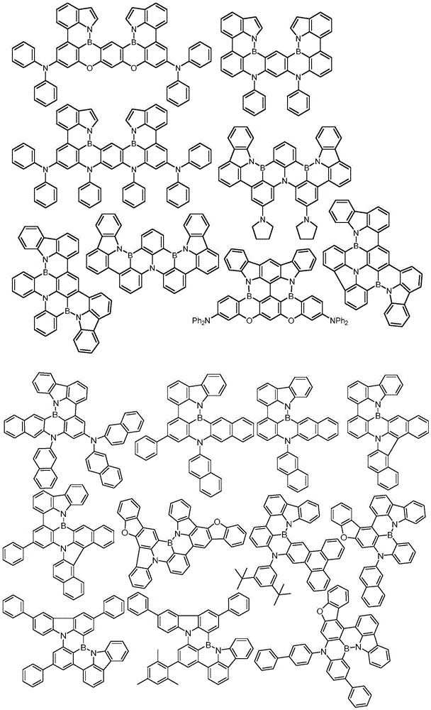

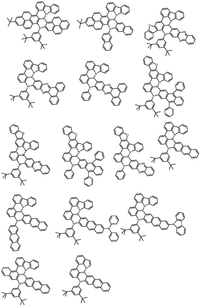


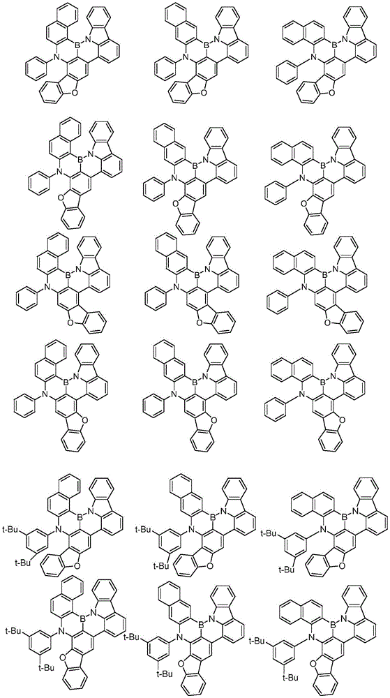
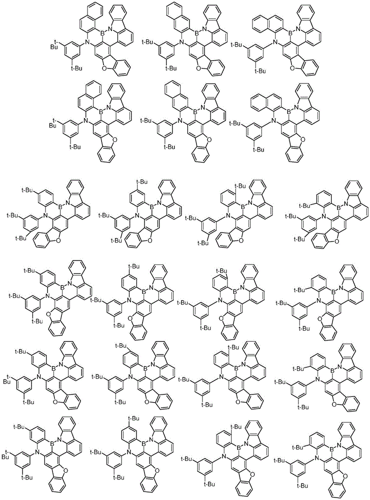


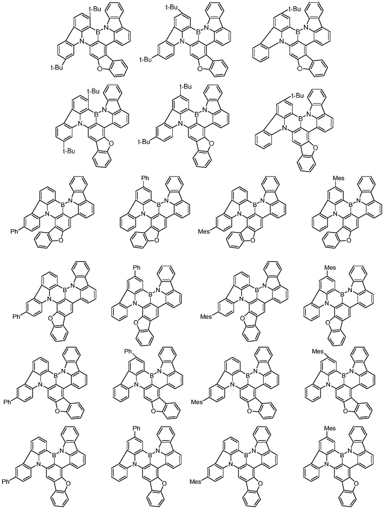


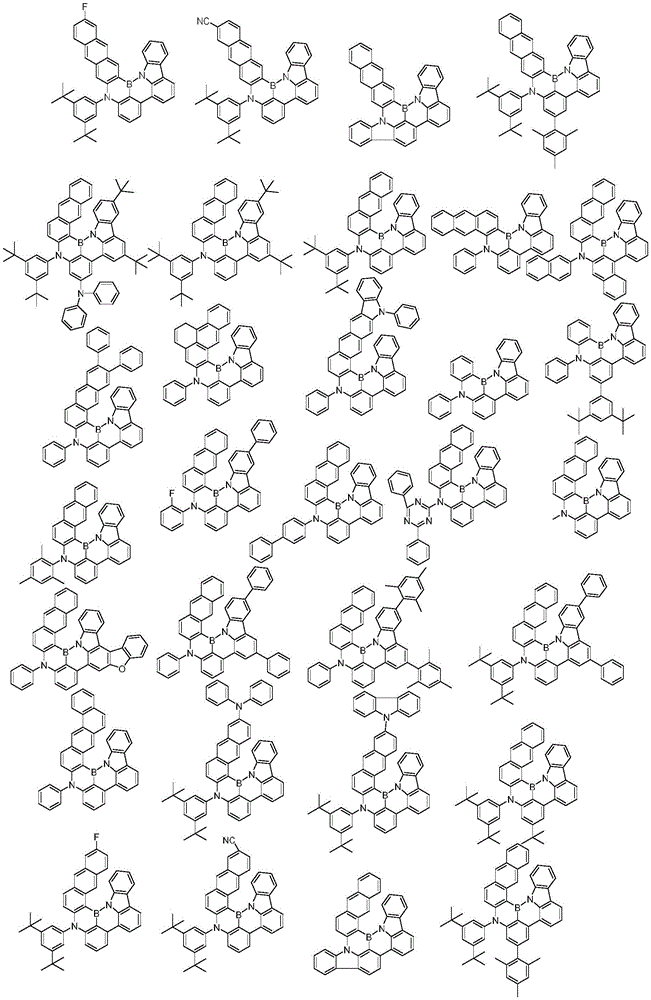


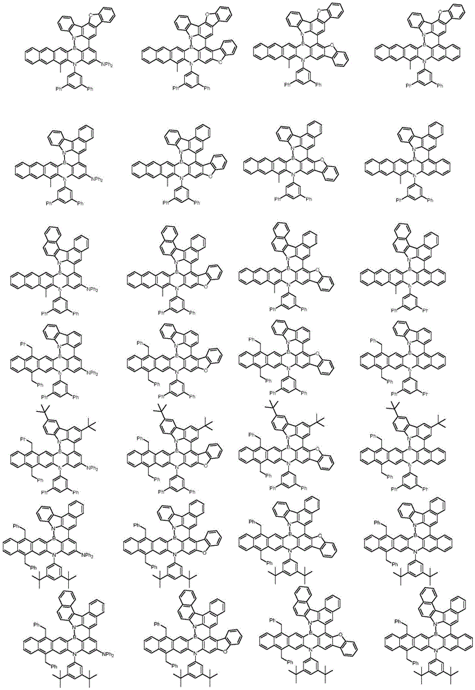
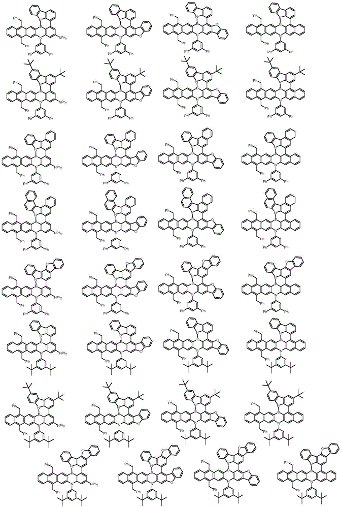


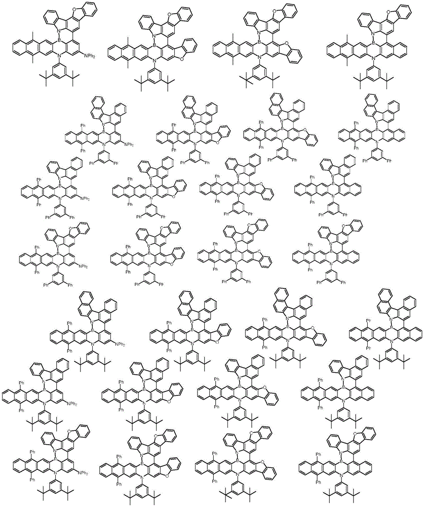
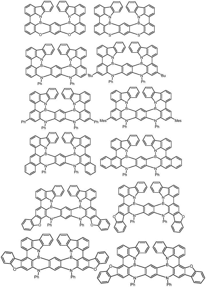

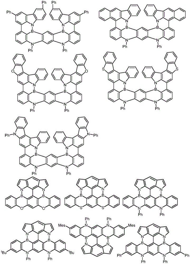


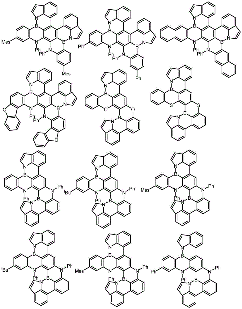

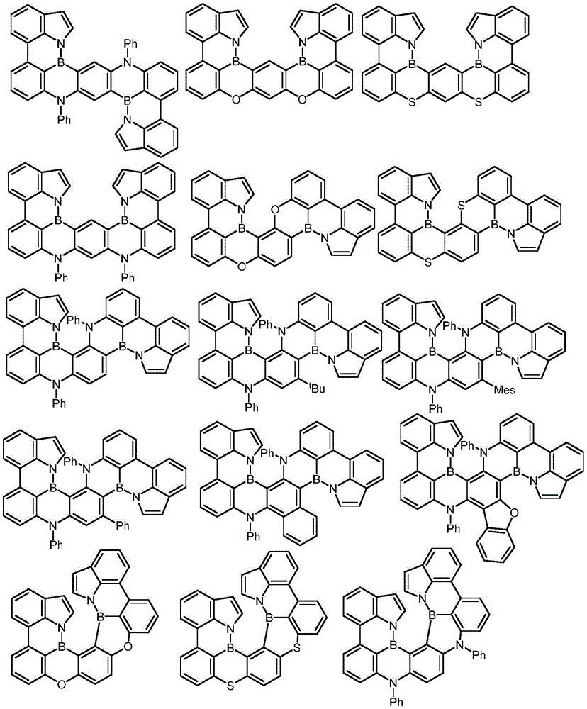


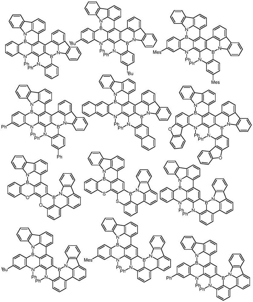

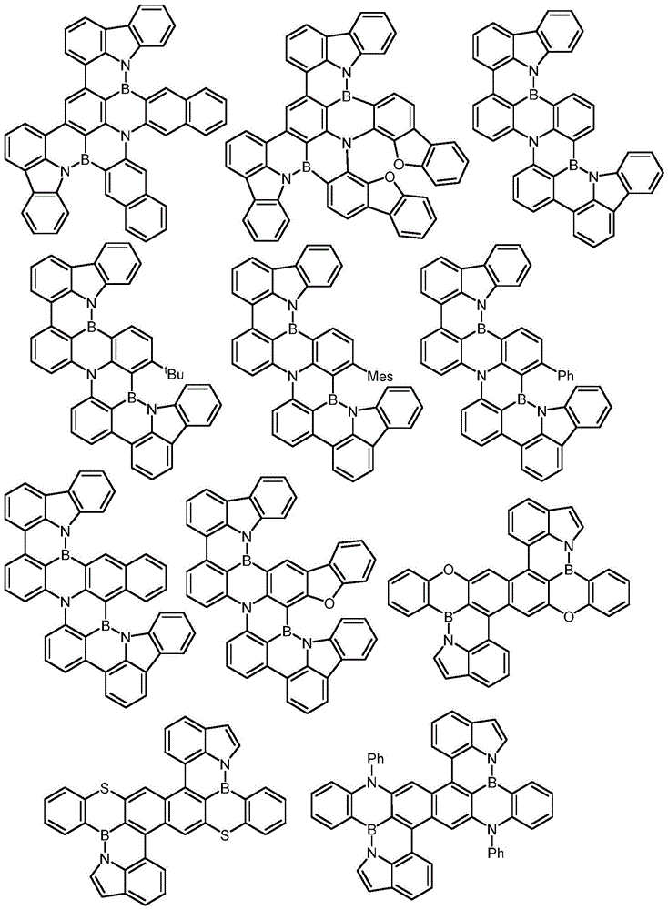


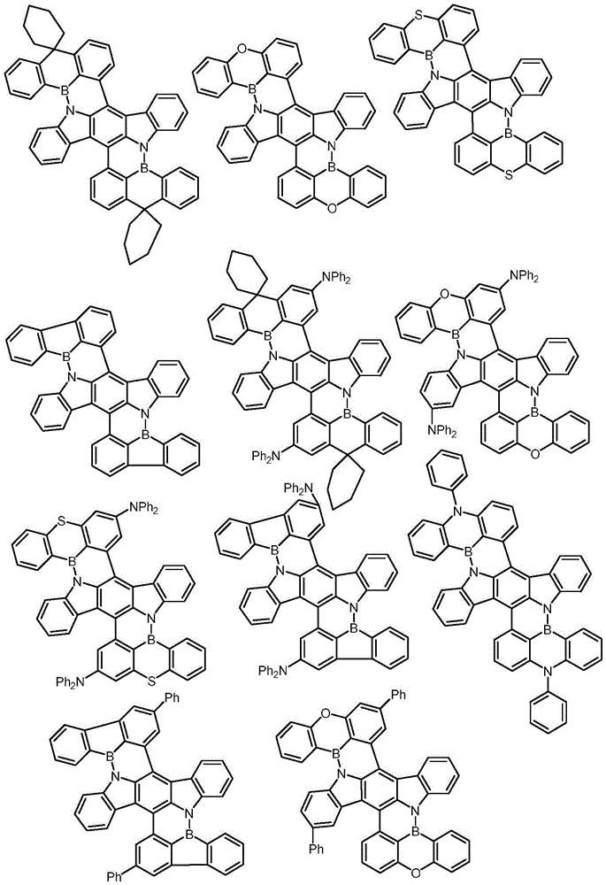
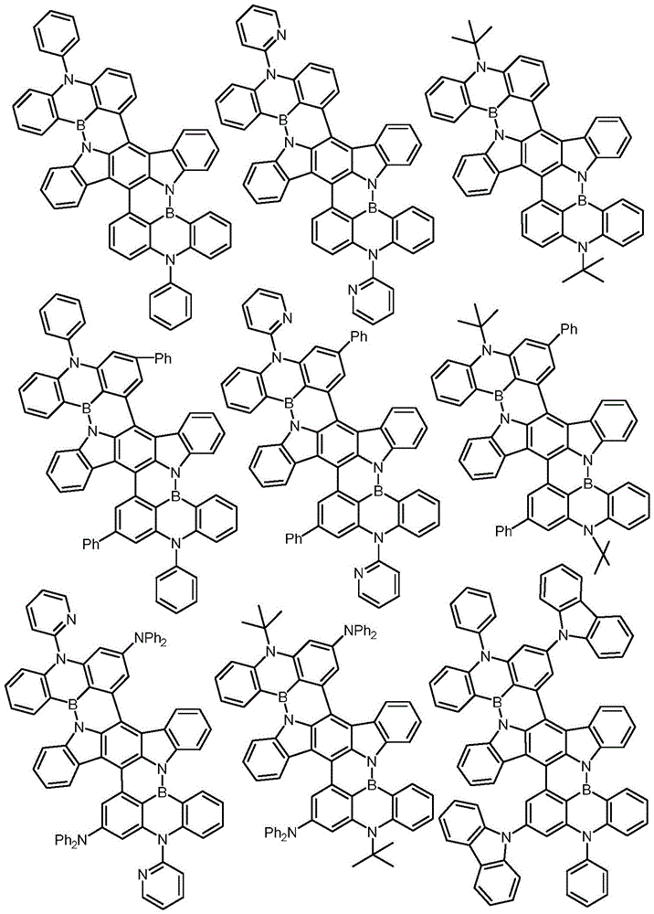

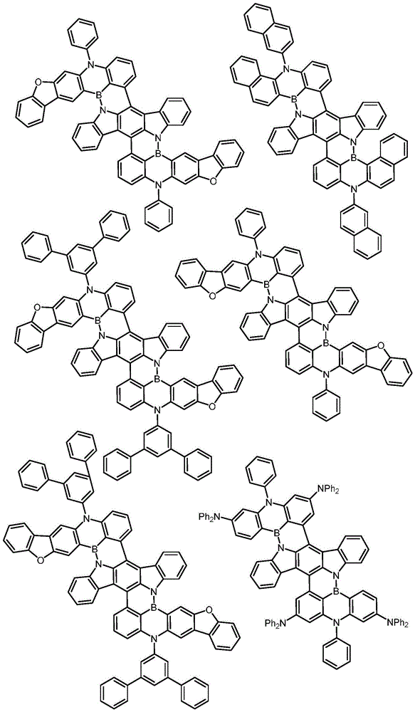


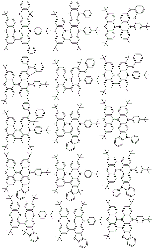


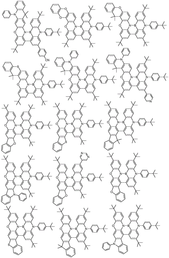
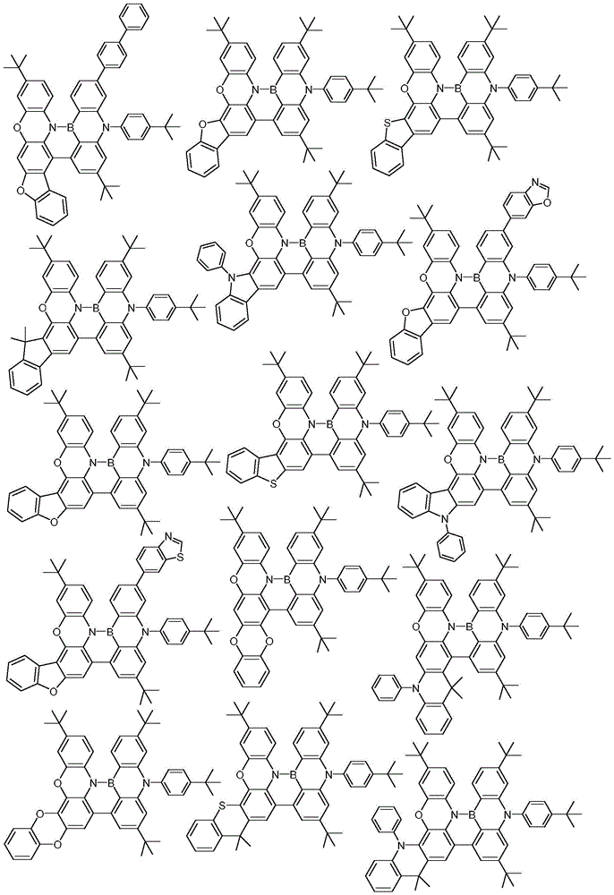


comprising or consisting of a structure according to formula BNE-1 B Can be accomplished via standard reactions and reaction conditions known to those skilled in the art.
Typically, the synthesis involves transition metal catalyzed cross-coupling reactions and boration reactions, all of which are known to those skilled in the art.
For example, WO2020135953 (A1) teaches how to synthesize small FWHM emitters S comprising or consisting of structures according to formula BNE-1 B . Furthermore, US2018047912 (A1) teaches how to synthesize small FWHM emitters S comprising or consisting of structures according to formula BNE-1 (in particular, c and d are 0) B 。
It is understood that the emitters disclosed in US2018047912 (A1) and WO2020135953 (A1) can also be used as small FWHM emitters S in the context of the present invention B 。
In one embodiment of the invention, in at least one (preferably each) light emitting layer B, at least one (preferably each) small FWHM emitter S B Comprising or consisting of a structure according to formula DABA-I or formula BNE-1. As understood by those skilled in the art, this means: if more than one small FWHM emitter S B In the light-emitting layer B, they may all comprise or consist of structures according to the formula DABA-I, or all comprise or consist of structures according to the formula BNE-1, or some of them may comprise or consist of structures according to the formula DABA-I, and others may comprise or consist of structures according to the formula BNE-1BNE-1.
One approach to designing fluorescent emitters relies on the use of fluorescent polycyclic aromatic or heteroaromatic core structures. In the context of the present invention, the latter is any structure comprising more than one aromatic or heteroaromatic ring (preferably more than two such rings), which are fused or linked to each other, even more preferably via more than one direct bond or linking atom. In other words, the fluorescent core structure comprises at least one (preferably only one) rigid conjugated pi-system.
One skilled in the art knows how to select a core structure for a fluorescent emitter, for example by US2017077418 (A1). Examples of common core structures of fluorescent emitters are listed below, wherein this does not imply that only these cores may provide a small FWHM emitter S suitable for use according to the invention B :


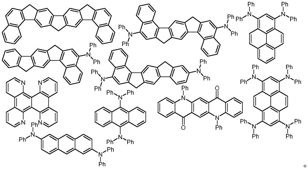
In this context, the term fluorescent core structure means that any molecule comprising a core can potentially be used as a fluorescent emitter. It is known to the person skilled in the art that the core structure of such fluorescent emitters may optionally be substituted and that these substituents are suitable in this respect, for example, by the following documents: US2017077418 (A1), M.Zhu.C.Yang, chemical Society Reviews, 2013,42,4963, DOI:10.1039/c3cs35440g; S.Kima, B.Kimb, J.Leea, H.Shina, Y. -Il Parkb, J.park, materials Science and Engineering R: reports 2016,99,1, DOI:10.1016/j.mser.2015.11.001; K.R.J.Thomas, N.Kapoor, M.N.K.P.Bolisetty, j. -h.jou, y. -l.chen, y. -c.jou, the Journal of Organic Chemistry 2012,77(8),3921,DOI:10.1021/jo300285v;M.Vanga,R.A.Lalancette,F. Chemistry–AEuropean Journal 2019,25(43),10133,DOI:10.1002/chem.201901231。
Small FWHM emitter S according to the invention B May be obtained by the above-described fluorescent core structure (e.g. by attaching sterically demanding substituents to the core) which hinder contact between the fluorescent core and adjacent molecules in the corresponding layer of the organic electroluminescent device.
In the context of the present invention, a compound (e.g., a fluorescent emitter) is considered to be spatially masked when the subsequently defined masking parameter is at or below a certain limit, which is also defined in the subsections that follow herein.
Preferably, the substituents of the fluorescent emitters for spatial shielding are not only bulky (i.e. space demanding) but also electronically inert, which in the context of the present invention means that these substituents do not comprise reactive atoms as defined in the subsections later herein. It is understood that this does not imply that only electronically inert (in other words: non-reactive) substituents may be attached to a fluorescent core structure (such as the one shown above). Reactive substituents may also be attached to the core structure and may be deliberately introduced to modulate the photophysical properties of the fluorescent core structure. In this case, it is preferred that the reactive atoms introduced via one or more substituents be shielded again by electronically inert (i.e., non-reactive) substituents.
Based on the above information and common knowledge from the prior art, the person skilled in the art understands how to select substituents for the fluorescent core structure, which substituents can induce steric shielding of the fluorescent core structure and are electronically inert as described above. In particular, US2017077418 (A1) discloses substituents suitable as electron-inert (in other words: non-reactive) shielding substituents. Examples of such substituents include straight-chain, branched chains having 3 to 40 carbon atoms (preferably 3 to 20 carbon atoms, more preferably 4 to 10 carbon atoms) A chain or cycloalkyl group in which one or more hydrogen atoms may be replaced by a substituent, preferably deuterium or fluorine. Other examples include alkoxy groups having 3 to 40 carbon atoms (preferably 3 to 20 carbon atoms, more preferably 4 to 10 carbon atoms), wherein one or more hydrogen atoms may be replaced by substituents, preferably deuterium or fluorine. It is understood that these alkyl and alkoxy substituents may be substituted with substituents other than deuterium and fluorine, for example, aryl. In this case, it is preferable that the aryl group as a substituent includes 6 to 30 aromatic ring atoms (more preferably, 6 to 18 aromatic ring atoms, most preferably, 6 aromatic ring atoms), and is preferably not a condensed aromatic system such as anthracene, pyrene, or the like. Other examples include aryl groups having 6 to 30 aromatic ring atoms (more preferably, having 6 to 24 aromatic ring atoms). One or more hydrogen atoms in these aryl substituents may be substituted, and preferred substituents are, for example, aryl groups having from 6 to 30 carbon atoms and straight, branched or cyclic alkyl groups having from 1 to 20 carbon atoms. All substituents may be further substituted. It is understood that all sterically demanding and preferably also electronically inert (in other words: non-reactive) substituents disclosed in US2017077418 (A1) can be used for sterically shielding a fluorescent core, such as the one described above, to provide a light emitting device suitable as a small FWHM emitter S for use in accordance with the present invention B Is provided.
In the following, non-limiting examples of substituents (disclosed in US2017077418 (A1)) that can be used as sterically demanding (i.e. shielded) and electronically inert (i.e. non-reactive) substituents in the context of the present invention are shown:


wherein each dashed line represents a single bond connecting the corresponding substituent to the core structure (preferably to the fluorescent core structure). As known to those skilled in the art, trialkylsilyl groups are also suitable for use as sterically demanding and electronically inert substituents.
It is also understood that the fluorescent core may not only have such sterically shielded substituents, but may also be substituted by a further non-shielding substituent which may or may not be an active group in the context of the present invention (see definition below).
In the following, a small FWHM emitter S is shown that can be used in the context of the present invention B Is illustrated for a spatially shielded fluorescent emitter. This does not imply that the invention is limited to organic electroluminescent devices comprising the emitters shown.
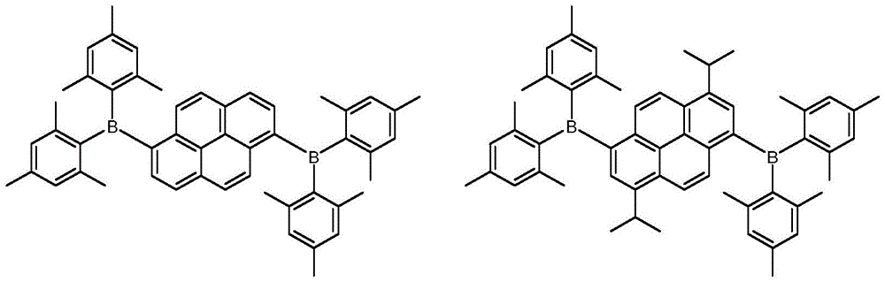
It is understood that the sterically shielding substituents (which may or may not be electronically inert as described above) may be attached to any fluorescent molecule (e.g., to the polycyclic aromatic or heteroaromatic fluorescent nuclei described above, the BODIPY-derived structures, and the NRCT emitters shown herein), and to emitters comprising the formula BNE-1 structures. This can result in a small FWHM emitter S which can be suitable as an emitter according to the invention B Is provided.
In one embodiment of the invention, in the light emitting layer B, a small FWHM emitter S B At least one of the following requirements is fulfilled:
(i) It is a boron (B) containing emitter, which means that each small FWHM emitter S B At least one atom in the ring is boron (B); and/or
(ii) It includes a polycyclic aromatic or heteroaromatic core structure in which at least two aromatic rings are fused together (e.g., anthracene, pyrene, or aza derivatives thereof).
In one embodiment of the invention, a small FWHM emitter S B Is a boron (B) containing emitter, which means that each small FWHM emitter S B Internal toOne atom less is boron (B).
In one embodiment of the invention, a small FWHM emitter S B Including polycyclic aromatic or heteroaromatic core structures in which at least two aromatic rings are fused together (e.g., anthracene, pyrene, or aza derivatives thereof).
In one embodiment of the invention, in the light emitting layer B, a small FWHM emitter S B At least one (or both) of the following requirements are met:
(i) It is a boron (B) containing emitter, which means that each small FWHM emitter S B At least one atom in the ring is boron (B); and/or
(ii) It includes a pyrene core structure.
In one embodiment of the invention, a small FWHM emitter S B Comprises a pyrene nucleus structure.
In a preferred embodiment of the invention, in the light-emitting layer B, a small FWHM emitter S B Is a boron (B) containing emitter and a nitrogen (N) containing emitter, which means that each small FWHM emitter S B At least one atom in the matrix is boron (B) and each small FWHM emitter S B At least one atom in the ring is nitrogen (N).
In a preferred embodiment of the invention, in the light-emitting layer B, a small FWHM emitter S B Comprising at least one boron atom (B) covalently bonded (directly) to at least one nitrogen atom (N).
In a preferred embodiment of the invention, in the light-emitting layer B, a small FWHM emitter S B Including trivalent (i.e., bound via three single bonds) boron atoms (B).
Space shield
Determination of masking parameter A
The shielding parameter a of the molecule may be determined as exemplarily described below for a (fluorescent) emitter, such as the (fluorescent) emitter mentioned above. It will be appreciated that the mask parameter a is generally referred to in angstroms This does not imply that only these compounds can be sterically shielded in the context of the present invention, nor that they are darkIt means that only masking parameters for these compounds can be determined.
1. Determination of energy level of molecular orbitals
The energy level of the molecular orbital can be determined via quantum chemistry. For this purpose, in the present case, the Turbomole software package (Turbomole GmbH), version 7.2, may be used. First, the geometry optimization of the ground state of the molecule can be performed using Density Functional Theory (DFT), employing the def2-SV (P) basis set and BP-86 functional. Then, based on the optimized geometry, a single point energy calculation for the electronic ground state can be performed using the B3-LYP functional. By energy calculation, for example, the Highest Occupied Molecular Orbital (HOMO) which is the highest energy orbital occupied by two electrons can be obtained, and the Lowest Unoccupied Molecular Orbital (LUMO) which is the lowest energy unoccupied orbital can be obtained. Energy levels may be obtained in a similar manner for other molecular orbitals (such as HOMO-1, HOMO-2,..lumo+1, lumo+2, etc.).
The method described herein is independent of the software package used. Examples of other commonly used programs for this purpose may be "Gaussian09" (Gaussian inc.) and Q-Chem 4.1 (Q-Chem, inc.).
2. Charge-exchange molecular orbitals of (fluorescent) compounds
The charge-exchanging molecular orbitals of (fluorescent) compounds can be considered to be both HOMO and LUMO and all molecular orbitals that can be separated from either HOMO or LUMO by 75meV or less in energy.
3. Determination of active atoms of molecular orbitals
For each charge exchange molecular orbital, it can be determined which atoms can be active. In other words, for each molecular orbital, a generally different set of reactive atoms can be found. How the active atoms of the HOMO can be determined is described below. The reactive atoms can be similarly determined for all other charge exchange molecular orbitals (e.g., HOMO-1, LUMO, LUMO+1, etc.).
HOMO can be calculated as described above. To determine the active atoms, the surface on which the orbit had an absolute value of 0.035 was examined ("the cut-off value was an isosurface of 0.035"). For this purpose, in the present case, jmol software (http:// Jmol. Sourceforge. Net /) is used, version 14.6.4. Atoms around which an orbital leaf having a value equal to or greater than a cutoff value may be located may be considered lively. Atoms around which an orbital leaf having a value equal to or greater than a cutoff value may not be located may be considered inactive.
4. Determination of active atoms in (fluorescent) compounds
An atom is considered to be active for a (fluorescent) compound if it is active in at least one charge-exchanging molecular orbital. Atoms that may be inactive (inactive) only in the entire charge-exchanging molecular orbital may be inactive for (fluorescent) compounds.
5. Determination of masking parameter A
In the first step, the solvent accessible surface area SASA for all reactive atoms can be determined according to the method described in B.Lee, F.M.Richards, journal of Molecular Biology 1971,55 (3), 379, DOI:10.1016/0022-2836 (71) 90324-X. For this purpose, the van der waals surface of the atoms of the molecule may be considered to be impenetrable. The SASA of the whole molecule can then be defined as the area of the surface that can be traced by the centre of a hard sphere (also called probe) with radius r (so-called probe radius), while it can roll over all accessible points in space where its surface can be in direct contact with the van der waals surface of the molecule. The SASA value may also be determined for a subset of atoms of the molecule. In this case, only the surface traced by the center of the probe at the point where the surface of the probe can contact the van der waals surface of atoms that may be part of the subset may be considered. The Lee-Richards algorithm for determining SASA for this purpose may be part of the package Free SASA (S.Mitternacht, free SASA: an open source C library for solvent accessible surface area computations.F1000Res.2016; 5:189.Published 2016Feb 18.doi:10.12688/f1000 research.7931.1). Van der Waals radius r of the relevant element VDW Can be compiled in the following references: M.Mantina, A.C.Chamberlin, R.Valero, C.J.Cramer, D.G.Truhlar, the Journal of Physical Chemistry A2009, 113 (19), 5806, DOI:10.1021/jp8111556. For this purpose, for all SASA determinations, the probe radius r may be set to
In the context of the present invention, the masking parameter a can be obtained by dividing the solvent accessible surface area of a subset of reactive atoms (labeled S to distinguish it from SASA of the whole molecule) by the number n of reactive atoms:
A=S/n。
in the context of the present invention, if the mask parameter A has a value below Value of->
 The compound may be defined as being well spatially shielded.
In the context of the present invention, if the mask parameter A has To->
To->
 (preferably,)>
 To->
To-> A compound may be defined as spatially masked.
In the following, exemplary (fluorescent) emitters are shown, together with their shielding parameters a determined as described above. It will be understood that this does not imply that the invention is limited to organic electroluminescent devices comprising one of the emitters shown. The depicted emitter compounds are merely non-limiting examples of alternative embodiments that represent the invention.

In one embodiment of the invention, each small FWHM emitter S comprised in the organic electroluminescent device according to the invention B Exhibit equal to or less than Is used for masking parameter a.
In one embodiment, in at least one (preferably each) light emitting layer B of the organic electroluminescent device according to the present invention, at least one (preferably each) small FWHM emitter S B Exhibit equal to or less than Is used for masking parameter a.
In a preferred embodiment of the invention, each small FWHM emitter S comprised in the organic electroluminescent device according to the invention B Exhibit equal to or less than Is used for masking parameter a.
In one embodiment, in at least one (preferably each) light emitting layer B of the organic electroluminescent device according to the present invention, at least one (preferably each) small FWHM emitter S B Exhibit equal to or less than Is used for masking parameter a.
It will be appreciated by those skilled in the art that not only small FWHM emitters S, such as those according to the present invention B May be spatially shielded by attaching a shielding substituent. It is understood, for example, that TADF material E in the context of the present invention B And phosphorescent material S in the context of the present invention B May also be shielded.
Excited state lifetime
A detailed description of how to measure excited state lifetime is provided in the subsections later herein.
In one embodiment of the invention, at least one (preferably each) TADF material E in the context of the invention is in the light-emitting layer B B Exhibits a delayed fluorescence lifetime of 110 μs or less (preferably 100 μs or less) In one embodiment of the invention, each TADF material E in the context of the invention B Exhibits a delayed fluorescence lifetime of equal to or less than 110 [ mu ] s (preferably, equal to or less than 100 [ mu ] s)>
In one embodiment of the invention, at least one (preferably each) TADF material E in the context of the invention is in the light-emitting layer B B Exhibiting a delayed fluorescence lifetime of 75 [ mu ] s or less In one embodiment of the invention, each TADF material E in the context of the invention B Exhibits a delayed fluorescence lifetime equal to or shorter than 75 mus>
In one embodiment of the invention, at least one (preferably each) TADF material E in the context of the invention is in the light-emitting layer B B Exhibiting a delayed fluorescence lifetime of 50 [ mu ] s or less In one embodiment of the invention, each TADF material E B Exhibits a delayed fluorescence lifetime of 50 [ mu ] s or less>
In a preferred embodiment of the invention, at least one (preferably each) TADF material E in the context of the invention is in the light-emitting layer B B Exhibiting a delayed fluorescence lifetime of 10 [ mu ] s or less In one embodiment of the invention, each TADF material E B Exhibits a delayed fluorescence lifetime of 10 mu s or less>
In an even more preferred embodiment of the invention, in the light emitting layer B, at least one (preferably each) TADF material E in the context of the invention B Exhibiting a delayed fluorescence lifetime of 5 μs or less In one embodiment of the invention, each TADF material E B Exhibits a delayed fluorescence lifetime of equal to or shorter than 5 mu s>
In one embodiment of the invention, in the luminescent layer B, the phosphorescent material P in the context of the invention B Exhibits an excited state lifetime of 50 [ mu ] s or less In one embodiment of the invention, each phosphor material P B Shows an excited state lifetime of 50 mus or less +.>
In a preferred embodiment of the invention, in the luminescent layer B, the phosphorescent material P in the context of the invention B Exhibits an excited state lifetime of 10 mu s or less In one embodiment of the invention, each phosphor material P B Exhibits an excited state lifetime of 10 mu s or less>
In an even more preferred embodiment of the invention, in the luminescent layer B, the phosphorescent material P in the context of the invention B Exhibits an excited state lifetime of 5 mu s or less In one embodiment of the invention, the phosphorescent material P B Exhibits an excited state lifetime of 5 mu s or less >
In one embodiment of the invention, in an organic electroluminescent device according to the invention, one or more TADF materials E B Added to include phosphorescent material P B Small FWHM emitter S B And a host material H B Resulting in a reduction in the excited state lifetime of the organic electroluminescent device in the light-emitting layer B. In a preferred embodiment of the invention, a TADF material E according to the invention B The above addition of (a) reduces the excited state lifetime of the organic electroluminescent device by at least 50%.
Further definition and information
As used throughout, the term "layer" in the context of the present invention preferably refers to a body having a broad planar geometry. It is understood that the same is true for all "sub-layers" that may make up a layer.
As used herein, the terms organic electroluminescent device and optoelectronic light emitting device and organic light emitting device may be understood in the broadest sense as any device comprising one or more light emitting layers B each comprising as a whole one or more TADF materials, one or more excitation energy transfer components EET-2, oneOne or more small FWHM emitters S B And optionally one or more host materials H B The above definitions and preferred embodiments may apply to all of these.
In a preferred embodiment of the invention, the organic electroluminescent device emits blue light at 440nm to 480 nm. In a preferred embodiment of the invention, the organic electroluminescent device has a main emission peak in the range of 440nm to 480 nm. In a preferred embodiment of the invention, the organic electroluminescent device has an emission maximum of a main emission peak in the range of 440nm to 480 nm.
In a particularly preferred embodiment of the invention, the organic electroluminescent device emits blue light of 450nm to 470 nm. In a particularly preferred embodiment of the invention, the organic electroluminescent device has a main emission peak in the range of 450nm to 470 nm. In a particularly preferred embodiment of the invention, the organic electroluminescent device has an emission maximum with a main emission peak in the range of 450nm to 470 nm.
In a preferred embodiment of the invention, the organic electroluminescent device is a device selected from the group consisting of an Organic Light Emitting Diode (OLED), a light emitting electrochemical cell (LEC) and a light emitting transistor.
Particularly preferably, the organic electroluminescent device is an Organic Light Emitting Diode (OLED). Alternatively, the organic electroluminescent device as a whole may be opaque (non-transparent), translucent or (substantially) transparent.
As used throughout this application, the term "cyclic group" may be understood in the broadest sense as any monocyclic, bicyclic, or polycyclic moiety.
As used throughout this application, the terms "ring" and "ring system" are to be understood in the broadest sense as any single, double or multiple ring moiety.
The term "ring atom" refers to any atom that is part of a ring or ring core of a ring structure, but not part of a substituent optionally attached thereto.
As used throughout this application, the term "carbocycle" may be understood in its broadest sense as any cyclic group in which the cyclic structure includes only carbon atoms, which may of course be substituted with hydrogen or any other substituent defined in the specific embodiments of the invention. It is understood that the term "carbocycle" as an adjective refers to a cyclic group wherein the cyclic structure comprises only carbon atoms, which of course may be substituted with hydrogen or any other substituent defined in the specific embodiments of the invention. It is understood that the term "carbocycle" or "carbocycle ring system" may refer to both aliphatic and aromatic ring groups or ring systems.
As used throughout this application, the term "heterocycle" may be understood in its broadest sense as any cyclic group in which the cyclic core structure includes not only carbon atoms but also at least one heteroatom. It is understood that the term "heterocycle" as an adjective refers to a cyclic group wherein the cyclic structure includes not only carbon atoms but also at least one heteroatom. Unless otherwise indicated in the specific examples, the heteroatoms may be the same or different at each occurrence and may be individually selected from the group consisting of N, O, S and Se. All carbon atoms or heteroatoms included in the heterocyclic ring in the context of the invention may of course be substituted with hydrogen or any other substituent defined in the specific embodiments of the invention. It is understood that the term "heterocycle" or "heterocyclic ring system" may refer to both aliphatic and heteroaromatic ring groups or ring systems.
As used throughout this application, the term "aromatic ring system" may be understood in the broadest sense as any bicyclic or polycyclic aromatic moiety.
As used throughout this application, the term "heteroaromatic ring system" may be understood in the broadest sense as any bicyclic or polycyclic heteroaromatic moiety.
As used throughout this application, the term "fused" when referring to an aromatic or heteroaromatic ring system means that the "fused" aromatic or heteroaromatic ring shares at least one bond that is part of both ring systems. For example, naphthalene (or naphthyl when referred to as a substituent) or benzothiophene (or benzothiophenyl when referred to as a substituent) are considered fused aromatic ring systems in the context of the present invention in which two benzene rings (for naphthalene) or thiophene and benzene (for benzothiophene) share one bond. It is also understood that sharing a bond in this context includes sharing two atoms that make up the respective bond, and that a fused aromatic or heteroaromatic ring system may be understood as one aromatic or heteroaromatic system. In addition, it is understood that more than one bond may be shared by the aromatic or heteroaromatic rings that make up the fused aromatic or heteroaromatic ring system (e.g., in pyrene). Furthermore, it will be understood that the alicyclic ring system may also be fused and this has the same meaning as for the aromatic or heteroaromatic ring system, except of course that the fused alicyclic ring system is not aromatic.
As used throughout this application, the terms "aryl" and "aromatic" are to be understood in the broadest sense as any monocyclic, bicyclic or polycyclic aromatic moiety. Here, unless otherwise indicated in the specific embodiments, aryl groups preferably contain 6 to 60 aromatic ring atoms, heteroaryl groups preferably contain 5 to 60 aromatic ring atoms, at least one of which is a heteroatom. Nevertheless, throughout the application, the number of aromatic ring atoms (specifically, the number of aromatic ring atoms as carbon atoms) may be given as a subscript number in the definition of certain substituents. In particular, the heteroaromatic ring includes one to three heteroatoms. Likewise, the terms "heteroaryl" and "heteroaromatic" are to be understood in the broadest sense as any monocyclic, bicyclic or polycyclic heteroaromatic moiety comprising at least one heteroatom. The heteroatoms may be the same or different at each occurrence and may be independently selected from the group consisting of N, O, S and Se. Thus, the term "arylene" refers to a divalent substituent having two points of attachment to other molecular structures and thus serving as a linker structure. In the case where the groups in the exemplary embodiments are defined differently from the definitions given herein (e.g., the number of aromatic ring atoms or the number of heteroatoms is different from the given definition), the definitions in the exemplary embodiments will apply. According to the invention, a condensed (cyclized) aromatic polycyclic or heteroaromatic polycyclic is composed of two or more mono-or heteroaromatic rings which form a polycyclic ring via a condensation reaction.
In particular, as used throughout this application, the term "aryl" or "heteroaryl" includes groups that may be bound via any position of an aromatic or heteroaromatic group, which groups are derived from benzene, naphthalene, anthracene, phenanthrene, pyrene, dihydropyrene, a, Perylene, fluoranthene, benzanthracene, benzophenanthrene, naphthacene, pentacene, benzopyrene, furan, benzofuran, isobenzofuran, dibenzofuran, thiophene, benzothiophene, isobenzothiophene, dibenzothiophene, selenophene, benzoselenophene, isobenzoselenophene, dibenzoselenophene, pyrrole, indole, isoindole, carbazole, pyridine, quinoline, isoquinoline, acridine, phenanthridine, benzo-5, 6-quinoline, benzo-6, 7-quinoline, benzo-7, 8-quinoline, phenothiazine, phenoxazine, pyrazole, indazole, imidazole, benzimidazole, naphthymidazole, phenanthroimidazole, pyridoimidazole pyrazine imidazole, quinoxaline imidazole, oxazole, benzoxazole, naphthooxazole, anthracene oxazole, phenanthro oxazole, isoxazole, 1, 2-thiazole, 1, 3-thiazole, benzothiazole, pyridazine, benzopyridazine, pyrimidine, benzopyrimidine, 1,3, 5-triazine, quinoxaline, pyrazine, phenazine, naphthyridine, carboline, benzocarboline, phenanthroline, 1,2, 3-triazole, 1,2, 4-triazole, benzotriazole, 1,2, 3-oxadiazole, 1,2, 4-oxadiazole, 1,2,3, 4-tetrazine, purine, pteridine, indolizine, and benzothiadiazole, or a combination of the foregoing.
In certain embodiments of the invention, adjacent substituents bound to an aromatic or heteroaromatic ring may together form an additional mono-or polycyclic aliphatic or aromatic or heteroaromatic carbocyclic or heterocyclic ring system fused to the aromatic or heteroaromatic ring to which the substituents are bound. It is understood that the fused ring system so formed will optionally be larger (meaning that it includes more ring atoms) than the aromatic or heteroaromatic ring to which the adjacent substituent is bound. In these cases, the "total" amount of ring atoms included in the fused ring system will be understood to be the sum of the ring atoms included in the aromatic or heteroaromatic ring to which the adjacent substituents are bound and the ring atoms of the additional ring system formed by the adjacent substituents, however, wherein the carbon atoms shared by the fused ring systems are counted once instead of twice. For example, the benzene ring may have two adjacent substituents that form another benzene ring so as to constitute a naphthalene nucleus. Because two carbon atoms are shared by two benzene rings and are therefore counted only once, rather than twice, the naphthalene nucleus then comprises 10 ring atoms. The term "adjacent substituent" in this context refers to a substituent attached to the same or adjacent ring atoms (e.g., of a ring system).
As used throughout this application, the term "aliphatic" when referring to a ring system is to be understood in the broadest sense and means that there are no aromatic or heteroaromatic rings in the ring that make up the ring system. It is understood that such an alicyclic ring system may be fused to one or more aromatic or heteroaromatic rings such that some (but not all) of the carbon atoms or heteroatoms included in the core structure of the alicyclic ring system are part of the attached aromatic or heteroaromatic ring.
As used above and herein, the term "alkyl" may be understood in its broadest sense as any linear, branched, or cyclic alkyl substituent. In particular, the term alkyl includes substituents such as: methyl (Me), ethyl (Et), n-propyl n Pr, isopropyl i Pr), cyclopropyl, n-butyl n Bu) and isobutyl% i Bu, sec-butyl% s Bu), t-butyl t Bu), cyclobutyl, 2-methylbutyl, n-pentyl, sec-pentyl, tert-pentyl, 2-pentyl, neopentyl, cyclopentyl, n-hexyl, sec-hexyl, tert-hexyl, 2-hexyl, 3-hexyl, neohexyl, cyclohexyl, 1-methylcyclopentyl, 2-methylpentyl, n-heptyl, 2-heptyl, 3-heptyl, 4-heptyl, cycloheptyl, 1-methylcyclohexyl, n-octyl, 2-ethylhexyl, cyclooctyl, 1-bicyclo [2,2 ]Octyl, 2-bicyclo [ 2.2.2]Octyl, 2- (2, 6-dimethyl) octyl, 3- (3, 7-dimethyl) octyl, adamantyl, 2-trifluoroethyl 1, 1-dimethyl-n-hex-1-yl, 1-dimethyl-n-hept-1-yl, 1-dimethyl-n-oct-1-yl, 1-dimethyl-n-dec-1-group, 1-dimethyl-n-dodecyl-1-group, 1-dimethyl-n-tetradecan-1-yl, 1-dimethyl-n-hexadecan-1-yl, 1-dimethyl-n-octadean-1-yl 1, 1-diethyl-n-hex-1-yl, 1-diethyl-n-hept-1-yl, 1-diethyl-n-oct-1-yl, 1-diethyl-n-dec-1-yl, 1-diethyl-n-dodec-1-yl 1, 1-diethyl-n-tetradecan-1-yl, 1-diethyl-n-hexadecan-1-yl, 1-diethyl-n-octadean-1-yl, 1- (n-propyl) -cyclohex-1-yl, 1- (n-butyl) -cyclohex-1-yl, 1- (n-hexyl) -cyclohex-1-yl, 1- (n-octyl) -cyclohex-1-yl and 1- (n-decyl) -cyclohex-1-yl.
As used above and herein, the term "alkenyl" includes straight-chain, branched-chain, and cyclic alkenyl substituents. The term alkenyl illustratively includes substituents such as: ethenyl, propenyl, butenyl, pentenyl, cyclopentenyl, hexenyl, cyclohexenyl, heptenyl, cycloheptenyl, octenyl, cyclooctenyl or cyclooctadienyl.
As used above and herein, the term "alkynyl" includes straight-chain, branched-chain, and cyclic alkynyl substituents. The term alkynyl illustratively includes ethynyl, propynyl, butynyl, pentynyl, hexynyl, heptynyl, or octynyl.
As used above and herein, the term "alkoxy" includes straight, branched, and cyclic alkoxy substituents. The term alkoxy illustratively includes methoxy, ethoxy, n-propoxy, isopropoxy, n-butoxy, isobutoxy, sec-butoxy, tert-butoxy and 2-methylbutoxy.
As used above and herein, the term "thioalkoxy" includes straight, branched, and cyclic thioalkoxy substituents wherein O of the exemplary alkoxy group is replaced with S.
As used above and herein, the terms "halogen" and "halo" are to be understood in the broadest sense as preferably fluorine, chlorine, bromine or iodine.
All hydrogen atoms (H) included in any of the structures mentioned herein may be replaced by deuterium (D) at each occurrence independently of each other and are not specifically indicated. It is common practice to replace hydrogen with deuterium and it will be apparent to those skilled in the art how to effect such a synthesis.
It is understood that when a fragment of a molecule is described as a substituent or otherwise attached to another moiety, its name may be written as if it were a fragment (e.g., naphthyl, dibenzofuranyl) or as if it were an entire molecule (e.g., naphthalene, dibenzofuranyl). As used herein, these different ways of specifying substituents or attachment fragments are considered equivalent.
When referring to concentration or composition, unless otherwise indicated, percentages refer to weight percentages having the same meaning as weight percentages or wt% ((weight/weight), (w/w), wt%).
The orbitals and excited state energies can be determined experimentally or by calculations employing quantum chemistry methods (specifically, density functional theory calculations). Here, the energy E of the highest occupied molecular orbital HOMO Determined by cyclic voltammetry measurements with an accuracy of 0.1eV by methods known to those skilled in the art.
Energy E of lowest unoccupied molecular orbital LUMO Can be determined by cyclic voltammetry measurements with an accuracy of 0.1eV by methods known to those skilled in the art. If E LUMO Can be determined by cyclic voltammetry measurements, which will be denoted herein as Alternatively, it is preferred here that E LUMO Calculated as E HOMO +E gap Wherein, unless otherwise indicated, for the host material H B TADF Material E B And a small FWHM emitter S B The energy of the first excited singlet S1 (see below) is used as E gap . That is, for the host material H B TADF Material E B And a small FWHM emitter S B ,E gap By the onset of the emission spectrum at room temperature (i.e., approximately 20 ℃) (steady-state spectrum; for TADF material E) B Typically 10 wt% E in poly (methyl methacrylate) (PMMA) is used B Is coated with a spin-on film; for small FWHM emitters S B Typically 1 to 5 wt% (preferably 2 wt%) S in PMMA is used B Is coated with a spin-on film; for the host material H B The corresponding host materials H are generally used B A spin-on pure film). For phosphorescent material P B ,E gap Also by the onset of the emission spectrum at room temperature (i.e., approximately 20 ℃) (typically by 10 wt% P in PMMA) B Spin-on film measurement of (c).
The absorption spectrum was recorded at room temperature (i.e., approximately 20 ℃). For TADF Material E B Typically by 10 wt% E in poly (methyl methacrylate) (PMMA) B Is used to measure the absorption spectrum. For small FWHM emitters S B Typically by 1 to 5 wt% (preferably 2 wt%) S in PMMA B Is used to measure the absorption spectrum. For the host material H B Typically by the host material H B Is used to measure the absorption spectrum. For phosphorescent material P B Typically by 10 wt% P in PMMA B Is used to measure the absorption spectrum. Alternatively, the absorption spectrum can also be recorded by a solution of the corresponding molecule (e.g. in methylene chloride or toluene), wherein the concentration of the solution is generally chosen such that the maximum absorbance is preferably in the range of 0.1 to 0.5.
The starting point of the absorption spectrum is determined by calculating the intersection of the tangent to the absorption spectrum with the x-axis. The tangent to the absorption spectrum is set at the low energy side of the absorption band and at the point of half height (half maximum) of the maximum intensity of the absorption spectrum.
Unless otherwise indicated, the energy of the first (i.e., lowest) excited triplet state T1 is determined by the onset of phosphorescence spectrum at 77K (for TADF material E B Typically 10 wt% E in PMMA is used B Is coated with a spin-on film; for small FWHM emitters S B Typically 1 to 5 wt% (preferably 2 wt%) S in PMMA is used B Is coated with a spin-on film; for the host material H B The corresponding host materials H are generally used B Is coated with a pure film by spin coating; for phosphorusOptical material P B Typically 10 wt% P in PMMA is used B And is typically measured at room temperature (i.e., approximately 20 ℃). As described in EP2690681A1, it is known that for a composition having a small Δe ST TADF Material E of value B Both intersystem crossing and reverse intersystem crossing can occur even at low temperatures. Thus, the emission spectrum at 77K may include emissions from both the S1 state and the T1 state. However, as also described in EP2690681A1, the contribution/value of triplet energy is generally considered to be dominant.
Unless otherwise indicated, the energy of the first (i.e., lowest) excited singlet S1 is determined by the onset of the fluorescence spectrum at room temperature (i.e., approximately 20 ℃) (steady state spectrum; for TADF material E B Typically 10 wt% E in PMMA is used B Is coated with a spin-on film; for small FWHM emitters S B Typically 1 to 5 wt% (preferably 2 wt%) S in PMMA is used B Is coated with a spin-on film; for the host material H B The corresponding host materials H are generally used B Is coated with a pure film by spin coating; for phosphorescent material P B Typically 10 wt% P in PMMA is used B A spin-on film of (c). However, for phosphorescent material P exhibiting efficient intersystem crossing B The room temperature emission may be (predominantly) phosphorescent and not fluorescent. In this case, the onset of the emission spectrum at room temperature (i.e., approximately 20 ℃) is used to determine the energy of the first (i.e., lowest) excited triplet state T1 as described above.
The starting point of the emission spectrum is determined by calculating the intersection of the tangent to the emission spectrum with the x-axis. The tangent to the emission spectrum is set at the high energy side of the emission band and at the point of half height (half maximum) of the maximum intensity of the emission spectrum.
ΔE corresponding to the energy difference between the first (i.e., lowest) excited singlet (S1) and the first (i.e., lowest) excited triplet (T1) ST The value is determined based on the first (i.e., lowest) excited singlet energy and the first (i.e., lowest) excited triplet energy determined as described above.
As known to those skilled in the artEmitters (e.g. small FWHM emitters S B ) The full width at half maximum (FWHM) is easily determined by the corresponding emission spectra (fluorescence spectrum for fluorescent emitters and phosphorescence spectrum for phosphorescent emitters). For small FWHM emitters S B Fluorescence spectroscopy is typically used. The total reported FWHM value generally refers to the main emission peak (i.e., the peak with the highest intensity). The manner in which the FWHM (preferably reported here in electron volts eV) is determined is part of the knowledge of the person skilled in the art. For example, consider that the main emission peak of the emission spectrum is at two wavelengths λ 1 And lambda (lambda) 2 At which half maximum emission (i.e. 50% of maximum emission intensity) is reached (the two wavelengths lambda 1 And lambda (lambda) 2 Both are obtained in nanometers (nm) by emission spectroscopy, and the FWHM in electron volts (eV) is typically (and here) determined using the following equation:
as used herein, if not more specifically defined in a specific context, the designation of the color of emitted and/or absorbed light is as follows:
purple: wavelength range >380nm to 420 nm;
deep blue: wavelength range >420nm to 475 nm;
sky blue: wavelength range from 475nm to 500 nm;
green: a wavelength range of >500nm to 560 nm;
yellow: wavelength range of >560nm to 580 nm;
orange: wavelength range of >580nm to 620 nm;
red: wavelength range of >620nm to 800 nm.
The invention is illustrated by the following examples and claims.
Example
Cyclic voltammetry
Measurement of a concentration of 10 in dichloromethane or a suitable solvent and a suitable supporting electrolyte -3 Solutions of organic molecules in mol/L (e.g0.1mol/L tetrabutylammonium hexafluorophosphate). Measurements were performed at room temperature (i.e., (approximately) 20 ℃) and under nitrogen atmosphere using a three electrode assembly (working and counter electrodes: pt wire, reference electrode: pt wire), and FeCp was used 2 /FeCp 2 + Calibration was performed as an internal standard. HOMO data and LUMO data were corrected for SCE using ferrocene as an internal standard.
Theoretical calculation of Density functional
The molecular structure was optimized using BP86 functional and consistency check method (RI, resolution of identity approach). The excitation energy is calculated using (BP 86) optimized structure using a time dependent DFT (TD-DFT) method. The Def2-SVP basis set and an m4 grid for numerical integration are used. The turbo program package is used for all calculations. The orbital and excited state energies were calculated using the B3LYP functional. Here, however, the orbitals and excited state energies are preferably determined experimentally as described above. All orbital and excited state energies reported herein have been experimentally determined (see experimental results).
Photophysical measurement
Sample pretreatment: evaporating in vacuum.
As described previously, each compound (e.g., organic molecule or transition metal complex) that may be included in the light emitting layer B of the organic electroluminescent device according to the present invention (e.g., host material H B TADF Material E B Phosphorescent material P B Or a small FWHM emitter S B ) Photophysical measurements of (a) typically use spin-on pure films (on host material H B In the case of poly (methyl methacrylate) (PMMA) or spin-on films of the corresponding materials in poly (methyl methacrylate) (PMMA) (e.g., for TADF material E) B Phosphorescent material P B And a small FWHM emitter S B ) To do so. These films are spin-on films, unless stated differently for a particular measurement, for TADF material E B And for phosphorescent material P B The concentration of the material in the PMMA film was 10 wt%, or S for a small FWHM emitter B The concentration of the material in the PMMA film is 1% to 5% by weight, preferably 2% by weight. Alternatively, as previously described, some photophysical measurements may also be performed by solutions of the corresponding molecules (e.gE.g., in methylene chloride or toluene), wherein the concentration of the solution is typically selected such that the maximum absorbance is preferably in the range of 0.1 to 0.5.
The device comprises: spin150, SPS euro.
The sample concentration was 1.0mg/mL, typically dissolved in toluene/DCM as a suitable solvent.
The procedure is as follows: 7 seconds to 30 seconds at 2000U/min. After coating, the film was dried at 70 ℃ for 1 minute.
For the purpose of further investigating the composition of certain materials as present in the EML of an organic electroluminescent device (according to the invention or comparative examples), samples for photophysical measurements were made by vacuum depositing the corresponding light emitting layer B of 50nm on a quartz substrate, by the same materials used for device fabrication. Photophysical characterization of the samples was performed under nitrogen atmosphere.
Absorption measurement
A Thermo Scientific Evolution UV-visible spectrophotometer was used to determine the wavelength of the absorption maximum of the sample in the wavelength region above 270 nm. The wavelength is used as excitation wavelength for photoluminescence spectra and quantum yield measurements.
Photoluminescence spectra
Steady state emission spectra were recorded using a Horiba Scientific, modell FluoMax-4 equipped with a 150W xenon arc lamp, excitation and emission monochromator. The sample was placed in a cuvette and flushed with nitrogen during the measurement.
Photoluminescence quantum yield measurement
For photoluminescence quantum yield (PLQY) measurements, the C9920-03G system (Hamamatsu Photonics) was measured using an integrating sphere, absolute PL quantum yield. The samples were kept under nitrogen throughout the measurement. The quantum yield was determined using software U6039-05 and is given in%. Yield was calculated using the equation:
wherein n is Photons (photon) Representing photon count, intStrength. For quality assurance, anthracene (known concentration) in ethanol was used as a reference.
TCSPC (time-dependent single photon count)
Unless otherwise stated in the context of certain embodiments or assays, an excited state particle number dynamics (excited state population dynamics) was determined using a Edinburgh Instruments FS5 fluorescence spectrophotometer equipped with an emission monochromator, a temperature stable photomultiplier as the detector unit, and a pulsed LED (310 nm center wavelength, 910ps pulse width) as the excitation source. The sample was placed in a cuvette and flushed with nitrogen during the measurement.
To determine the average decay time of a measured transient photoluminescence signal The data were fitted with the sum of n exponential functions:

wherein n is an integer between 1 and 3. By setting a specific decay time constant tau i Corresponding to amplitude A i Weighting, determining excited state lifetime

The method can be used for fluorescent and phosphorescent materials to determine excited state lifetime. For TADF materials, the full decay kinetics described below need to be collected.
Full decay kinetics
By having a window of time of 4: TCSPC measurements were made in longer measurements of 200ns, 1 μs and 20 μs spanning >80 μs to achieve full excited state particle number decay kinetics over several orders of magnitude in time and signal intensity. The measured time profile is then processed in the following manner:
background correction is applied by determining the average signal level prior to excitation and subtraction.
The time axis is aligned by taking the initial rise of the main signal as a reference.
The curves are scaled to each other using overlapping measurement time regions.
The processed curves are combined into one curve.
Data analysis was performed using single and double exponential fits with decay of fluorescence on demand (PF) and Delayed Fluorescence (DF), respectively. The specific decay time constant tau obtained by fitting i Corresponding to amplitude A i Weighting, the average lifetimes of the instant (i.e., instant fluorescence lifetime) and delayed fluorescence (i.e., delayed fluorescence lifetime) can be determined separately as follows

Wherein n is 1 or 2.
The ratio of delayed fluorescence to instant fluorescence (n-value) is calculated by integration of the corresponding photoluminescence decay over time.

Transient photoluminescence measurement with spectral resolution
In transient Photoluminescence (PL) measurements with spectral resolution, the PL spectrum at a specified delay time after pulsed light excitation is recorded.
An exemplary apparatus for measuring transient PL spectra includes:
a pulsed laser (eMOPA, cryLas) with a center wavelength of 355nm and a pulse width of 1ns is used to excite the sample.
A sample chamber configured to hold a sample that can be evacuated or flushed with nitrogen.
A spectrometer (spectropro HRS) for dispersing light emitted from the sample.
A CCD camera (Princeton Instruments PI-MAX 4) with an integrated timing generator synchronized with the pulsed laser for wavelength-resolved detection of the scattered emitted light.
A personal computer configured to analyze signals inputted thereto from the CCD camera.
During the measurement, the sample is placed in a sample chamber and irradiated with a pulsed laser. The emitted light from the sample was acquired in a direction 90 degrees with respect to the irradiation direction of the laser pulse. It is dispersed by a spectrometer and directed onto a detector (a CCD camera in an exemplary device) to obtain a wavelength resolved emission spectrum. The time delay between laser irradiation and detection and the duration of detection (i.e., the control time) are controlled by a timing generator.
It should be noted that transient photoluminescence may be measured by a different device than that described in the exemplary device.
Fabrication and characterization of organic electroluminescent devices
OLED devices comprising organic molecules according to the invention can be manufactured via vacuum deposition methods. If a layer contains more than one compound, the weight percentage of one or more compounds is given in%. The total weight percentage value is 100% and therefore if no value is given, the fraction of this compound is equal to the difference between the given value and 100%.
The incompletely optimized OLEDs were characterized using standard methods and measuring electroluminescence spectra, the external quantum efficiency (in%) dependent on intensity calculated using light and current detected by photodiodes. The FWHM of the device is determined by the electroluminescence spectrum as previously stated for photoluminescence spectra (fluorescence or phosphorescence). The reported FWHM refers to the main emission peak (i.e., the peak with the highest emission intensity). OLED device lifetime is extracted by the change in brightness during operation at constant current density. The LT50 value corresponds to a point in time when the measured luminance decreases to 50% of the initial luminance, similarly, the LT80 value corresponds to a point in time when the measured luminance decreases to 80% of the initial luminance, the LT97 value corresponds to a point in time when the measured luminance decreases to 97% of the initial luminance, and so on.
Accelerated life measurements are made (e.g., using increased current density). Illustratively, the following equation is used to determine the value at 500cd/m 2 The following LT80 values:
wherein L is 0 Representing the initial brightness at the applied current density. This value corresponds to the average of several (typically two to eight) pixels.
Experimental results
Stacked material


TTA material

Table 1tta. Properties of tta material.
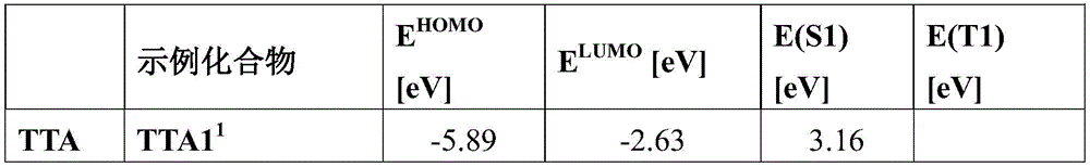
1 Measured in pure film.
Host material H B

Table 1H. Properties of host materials.
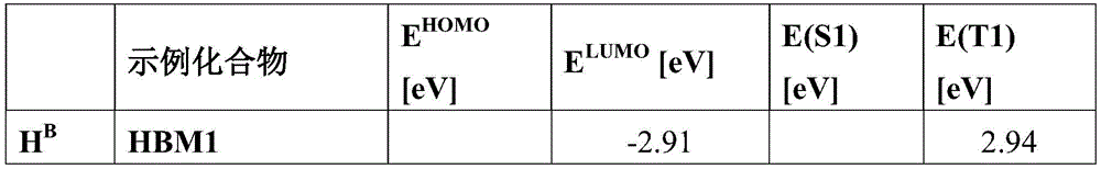
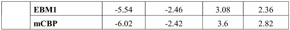
Can be selected as TADF material E B Or TADF material E for exciting energy transfer component EET-2 B
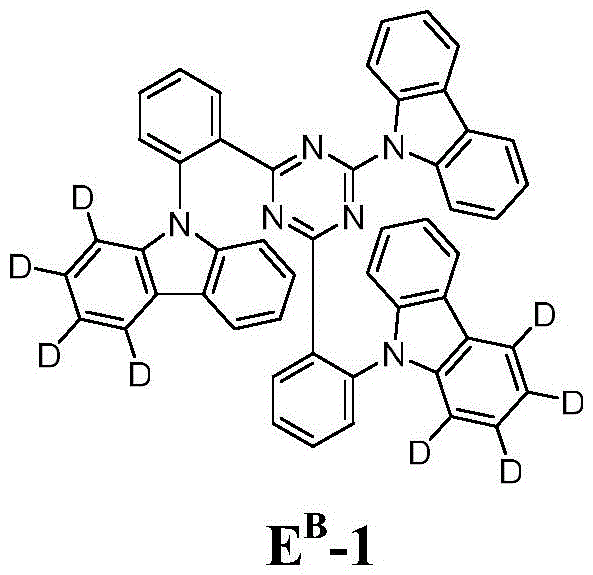
TABLE 1E TADF Material E B Properties of (3)
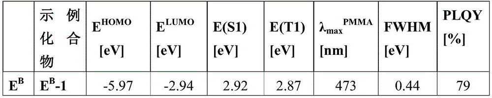
Phosphorescent material P which may be selected as excitation energy transfer component EET-2 B

Table 1P. Properties of phosphorescent materials.

Wherein,, is the energy of the lowest unoccupied molecular orbital, which is determined by cyclic voltammetry. c Emission spectrum passing through 0.001mg/mL P B -3 recording of the solution in toluene.
Small FWHM emitter S B

TABLE 1S Small FWHM emitter S B Is a property of (a).


Table 2. Exemplary organic electroluminescent device (OLED) settings 1.

Results I: EET-2 is the phosphorescent material P in the light-emitting layer B (the emission layer 5) B The composition of the light-emitting layer B of device D1 (percentages refer to weight percent):

set 1 from table 2 was used, wherein mCBP (H B -1) use as host material H B ,E B -1 use as TADF Material E B ,P B 3 is used as excitation energy transfer component EET-2 (here exemplified by phosphorescent material P B ) And S is B -15 as small FWHM emitter S B 。
Device results I
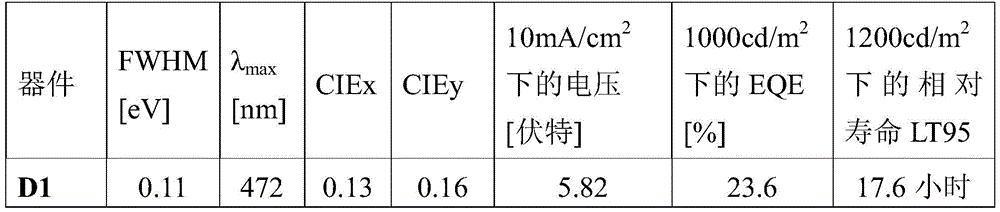
Table 3. Exemplary organic electroluminescent device (OLED) settings 2.

Results II: EET-2 is a phosphorescent material P in the light-emitting layer B (the emission layer 6) and the exciton management layer EXL adjacent to the light-emitting layer B B
The composition of the light-emitting layer B of device D2 (percentages refer to weight percent):

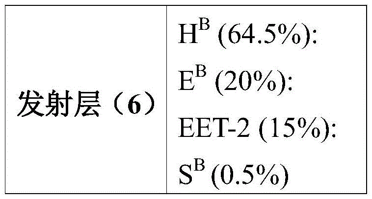
setting 2 from table 3 was used, wherein mCBP (H B -1) use as host material H B ,E B -1 use as TADF Material E B ,P B 3 is used as excitation energy transfer component EET-2 (here exemplified by phosphorescent material P B ) And S is B -15 as small FWHM emitter S B 。
Device results II

Claims (15)
1. An organic electroluminescent device comprising a light emitting layer B comprising the following components:
(i) TADF Material E B With a lowest excited singlet energy level E (S1 E ) And a lowest excited triplet level E (T1 E );
(ii) Small Full Width Half Maximum (FWHM) emitter S B With a lowest excited singlet energy level E (S1 S ) And a lowest excited triplet level E (T1 S ) Wherein S is B Emitting light having an emission maximum between 440nm and 480nm and having a full width at half maximum (FWHM) of less than or equal to 0.25 eV; and
(iii) Host material H B With a lowest excited singlet energy level E (S1 H ) And a lowest excited triplet level E (T1 H );
Wherein the organic electroluminescence includes an exciton management layer EXL adjacent to the light emitting layer B, the exciton management layer EXL including a triplet-triplet annihilation (TTA) material.
2. The organic electroluminescent device of claim 1, wherein the exciton management layer EXL has a thickness less than 15 nm.
3. The organic electroluminescent device according to claim 1 or 2, wherein the exciton management layer EXL has a thickness of less than 10 nm.
4. The organic electroluminescent device according to one or more of claims 1 to 3, wherein the TTA material comprises a structure represented by formula 4:

wherein,,
each Ar is independently selected from the group consisting of: c (C) 6 -C 60 Aryl optionally substituted with a member selected from the group consisting of C 6 -C 60 Aryl, C 3 -C 57 Heteroaryl, halogen and C 1 -C 40 One or more residues of the group consisting of (hetero) alkyl groups; c 3 -C 57 Heteroaryl optionally substituted with a member selected from C 6 -C 60 Aryl, C 3 -C 57 Heteroaryl, halogen and C 1 -C 40 One or more residues of the group consisting of (hetero) alkyl groups; and is also provided with
Each A 1 Independently selected from the group consisting of: hydrogen; deuterium; c (C) 6 -C 60 Aryl optionally substituted with a member selected from the group consisting of C 6 -C 60 Aryl, C 3 -C 57 Heteroaryl, halogen and C 1 -C 40 (hetero) alkylOne or more residues in the group consisting of; c (C) 3 -C 57 Heteroaryl optionally substituted with a member selected from C 6 -C 60 Aryl, C 3 -C 57 Heteroaryl, halogen and C 1 -C 40 One or more residues of the group consisting of (hetero) alkyl groups; c 1 -C 40 (hetero) alkyl optionally substituted with a member selected from the group consisting of C 6 -C 60 Aryl, C 3 -C 57 Heteroaryl, halogen and C 1 -C 40 One or more residues of the group consisting of (hetero) alkyl groups.
5. The organic electroluminescent device according to one or more of claims 1 to 4, wherein the adjacent layer EXL comprises at least one additional emitter.
6. The organic electroluminescent device according to one or more of claims 1 to 5, wherein the emitters in the adjacent layer and the light emitting layer B are both small Full Width Half Maximum (FWHM) emitters S B The small Full Width Half Maximum (FWHM) emitter S B Light is emitted having a full width at half maximum (FWHM) of less than or equal to 0.25eV and having an emission maximum between 440nm and 480 nm.
7. The organic electroluminescent device according to one or more of claims 1 to 6, wherein the light emitting layer B further comprises the following components:
(iv) Excitation energy transfer component EET-2 having the lowest excitation singlet energy level E (S1) EET-2 ) And a lowest excited triplet level E (T1 EET-2 ) The method comprises the steps of carrying out a first treatment on the surface of the And the excitation energy transfer component EET-2 is selected from the group consisting of TADF materials and phosphorescent materials.
8. The organic electroluminescent device of claim 7, wherein EET-2 is a phosphorescent material.
9. The organic electroluminescent device according to one or more of claims 1 to 8, wherein theThe small FWHM emitter S B At least one of the following requirements is fulfilled:
(i) It is a boron (B) containing emitter, which means that each small FWHM emitter S B At least one atom in the ring is boron (B); and/or
(ii) It includes a polycyclic aromatic or heteroaromatic core structure in which at least two aromatic rings are fused together (such as for example anthracene, pyrene, or aza derivatives thereof).
10. The organic electroluminescent device according to one or more of claims 1 to 9, wherein each TADF material E B :
(i) Characterized by exhibiting a delta E of less than 0.4eV ST Value of delta E ST The value corresponds to the lowest excited singlet energy E (S1 E ) And the lowest excited triplet energy E (T1) E ) Energy difference between them; and is also provided with
(ii) Shows a photoluminescence quantum yield (PLQY) of more than 30%.
11. The organic electroluminescent device according to one or more of claims 1 to 10, wherein one of the following conditions is satisfied:
(i)E(T1 EET-2 )>E(T1 E ) And E (T1) EET-2 )–E(S1 E ) Less than or equal to 0.3eV; or alternatively
(ii)E(T1 E )>E(T1 EET-2 ) And E (T1) E )–E(S1 E )≤0.3eV。
12. The organic electroluminescent device according to one or more of claims 1 to 11, wherein the exciton management layer EXL is located between the light emitting layer B and an anode of the organic electroluminescent device.
13. A method for producing an organic electroluminescent device according to any one of claims 1 to 12, comprising the steps of:
(i) Evaporating the light emitting layer B via vacuum deposition; and
(ii) The exciton management layer EXL is evaporated via vacuum deposition,
wherein said step (i) and said step (ii) are performed sequentially with each other, and
the order of said steps (i) and (ii) can be reversed.
14. A method for generating light, the method comprising the steps of:
(i) Providing an organic electroluminescent device according to any one of claims 1 to 12 or obtainable by the method of claim 13; and
(ii) A current is applied to the organic electroluminescent device.
15. The method of claim 14, wherein the method is used to produce light having an emission maximum with a main emission peak within a wavelength of 440nm to 480 nm.
Applications Claiming Priority (35)
| Application Number | Priority Date | Filing Date | Title |
|---|---|---|---|
| EP20197075 | 2020-09-18 | ||
| EP20197071 | 2020-09-18 | ||
| EP20197074 | 2020-09-18 | ||
| EP20197073 | 2020-09-18 | ||
| EP20197072.0 | 2020-09-18 | ||
| EP20197076.1 | 2020-09-18 | ||
| EP20197075.3 | 2020-09-18 | ||
| EP20197072 | 2020-09-18 | ||
| EP20197076 | 2020-09-18 | ||
| EP20197073.8 | 2020-09-18 | ||
| EP20197071.2 | 2020-09-18 | ||
| EP20197074.6 | 2020-09-18 | ||
| EP20197589 | 2020-09-22 | ||
| EP20197588.5 | 2020-09-22 | ||
| EP20197589.3 | 2020-09-22 | ||
| EP20197588 | 2020-09-22 | ||
| EP20217041.1 | 2020-12-23 | ||
| EP20217041 | 2020-12-23 | ||
| EP21170779.9 | 2021-04-27 | ||
| EP21170783.1 | 2021-04-27 | ||
| EP21170776.5 | 2021-04-27 | ||
| EP21170775.7 | 2021-04-27 | ||
| EP21170776 | 2021-04-27 | ||
| EP21170779 | 2021-04-27 | ||
| EP21170775 | 2021-04-27 | ||
| EP21170783 | 2021-04-27 | ||
| EP21184619 | 2021-07-08 | ||
| EP21184619.1 | 2021-07-08 | ||
| EP21184616 | 2021-07-08 | ||
| EP21184616.7 | 2021-07-08 | ||
| EP21185402.1 | 2021-07-13 | ||
| EP21185402 | 2021-07-13 | ||
| EP21186615 | 2021-07-20 | ||
| EP21186615.7 | 2021-07-20 | ||
| PCT/EP2021/075655 WO2022058523A1 (en) | 2020-09-18 | 2021-09-17 | Organic electroluminescent device emitting blue light |
Publications (1)
| Publication Number | Publication Date |
|---|---|
| CN116235645A true CN116235645A (en) | 2023-06-06 |
Family
ID=78049190
Family Applications (15)
| Application Number | Title | Priority Date | Filing Date |
|---|---|---|---|
| CN202180063847.2A Pending CN116368957A (en) | 2020-09-18 | 2021-09-17 | Organic Electroluminescent Devices |
| CN202180064156.4A Pending CN116261920A (en) | 2020-09-18 | 2021-09-17 | Organic Electroluminescent Devices |
| CN202180063926.3A Pending CN116235643A (en) | 2020-09-18 | 2021-09-17 | Organic electroluminescent device emitting green light |
| CN202180064202.0A Pending CN116264871A (en) | 2020-09-18 | 2021-09-17 | Organic Electroluminescent Devices Emitting Blue Light |
| CN202180063829.4A Pending CN116261919A (en) | 2020-09-18 | 2021-09-17 | Organic Electroluminescent Devices |
| CN202180064271.1A Pending CN116235644A (en) | 2020-09-18 | 2021-09-17 | Organic Electroluminescent Devices |
| CN202180064207.3A Pending CN116326240A (en) | 2020-09-18 | 2021-09-17 | Organic Electroluminescent Devices |
| CN202180064324.XA Pending CN116235647A (en) | 2020-09-18 | 2021-09-17 | Organic Electroluminescent Devices |
| CN202180063835.XA Pending CN116235648A (en) | 2020-09-18 | 2021-09-17 | Organic Electroluminescent Devices |
| CN202180064299.5A Pending CN116391456A (en) | 2020-09-18 | 2021-09-17 | Organic electroluminescent device |
| CN202180064334.3A Pending CN116261921A (en) | 2020-09-18 | 2021-09-17 | Organic Electroluminescent Devices |
| CN202180064229.XA Pending CN116235646A (en) | 2020-09-18 | 2021-09-17 | Organic Electroluminescent Devices |
| CN202180063466.4A Pending CN116368956A (en) | 2020-09-18 | 2021-09-17 | Organic electroluminescent device |
| CN202180064322.0A Pending CN116235645A (en) | 2020-09-18 | 2021-09-17 | Organic Electroluminescent Devices Emitting Blue Light |
| CN202180064226.6A Pending CN116210360A (en) | 2020-09-18 | 2021-09-17 | Organic Electroluminescent Devices |
Family Applications Before (13)
| Application Number | Title | Priority Date | Filing Date |
|---|---|---|---|
| CN202180063847.2A Pending CN116368957A (en) | 2020-09-18 | 2021-09-17 | Organic Electroluminescent Devices |
| CN202180064156.4A Pending CN116261920A (en) | 2020-09-18 | 2021-09-17 | Organic Electroluminescent Devices |
| CN202180063926.3A Pending CN116235643A (en) | 2020-09-18 | 2021-09-17 | Organic electroluminescent device emitting green light |
| CN202180064202.0A Pending CN116264871A (en) | 2020-09-18 | 2021-09-17 | Organic Electroluminescent Devices Emitting Blue Light |
| CN202180063829.4A Pending CN116261919A (en) | 2020-09-18 | 2021-09-17 | Organic Electroluminescent Devices |
| CN202180064271.1A Pending CN116235644A (en) | 2020-09-18 | 2021-09-17 | Organic Electroluminescent Devices |
| CN202180064207.3A Pending CN116326240A (en) | 2020-09-18 | 2021-09-17 | Organic Electroluminescent Devices |
| CN202180064324.XA Pending CN116235647A (en) | 2020-09-18 | 2021-09-17 | Organic Electroluminescent Devices |
| CN202180063835.XA Pending CN116235648A (en) | 2020-09-18 | 2021-09-17 | Organic Electroluminescent Devices |
| CN202180064299.5A Pending CN116391456A (en) | 2020-09-18 | 2021-09-17 | Organic electroluminescent device |
| CN202180064334.3A Pending CN116261921A (en) | 2020-09-18 | 2021-09-17 | Organic Electroluminescent Devices |
| CN202180064229.XA Pending CN116235646A (en) | 2020-09-18 | 2021-09-17 | Organic Electroluminescent Devices |
| CN202180063466.4A Pending CN116368956A (en) | 2020-09-18 | 2021-09-17 | Organic electroluminescent device |
Family Applications After (1)
| Application Number | Title | Priority Date | Filing Date |
|---|---|---|---|
| CN202180064226.6A Pending CN116210360A (en) | 2020-09-18 | 2021-09-17 | Organic Electroluminescent Devices |
Country Status (6)
| Country | Link |
|---|---|
| US (15) | US20230329021A1 (en) |
| EP (20) | EP4214771B1 (en) |
| JP (14) | JP2023541975A (en) |
| KR (13) | KR20230068390A (en) |
| CN (15) | CN116368957A (en) |
| WO (15) | WO2022058525A1 (en) |
Families Citing this family (9)
| Publication number | Priority date | Publication date | Assignee | Title |
|---|---|---|---|---|
| US8965580B2 (en) | 2012-06-21 | 2015-02-24 | Rethink Robotics, Inc. | Training and operating industrial robots |
| US12522565B2 (en) | 2019-10-25 | 2026-01-13 | Universal Display Corporation | Organic electroluminescent materials and devices |
| JP2023050136A (en) * | 2021-09-29 | 2023-04-10 | 住友化学株式会社 | Composition and light emitting element containing the same |
| CN117327056A (en) * | 2022-06-30 | 2024-01-02 | 北京夏禾科技有限公司 | Organic electroluminescent material and device thereof |
| EP4335846A1 (en) * | 2022-06-30 | 2024-03-13 | Beijing Summer Sprout Technology Co., Ltd. | Organic electroluminescent material and device thereof |
| US20240188316A1 (en) * | 2022-10-27 | 2024-06-06 | Universal Display Corporation | Organic electroluminescent materials and devices |
| CN117229197A (en) * | 2023-09-08 | 2023-12-15 | 辽宁师范大学 | A carbazole derivative with AEE characteristics and its preparation method and application |
| KR20250145343A (en) * | 2024-03-28 | 2025-10-13 | 삼성에스디아이 주식회사 | Compound for organic optoelectronic device, composition for organic optoelectronic device, organic optoelectronic device and display device |
| WO2025256635A1 (en) * | 2024-06-14 | 2025-12-18 | 浙江光昊光电科技有限公司 | Mixture, composition, and use thereof in photoelectric field |
Family Cites Families (178)
| Publication number | Priority date | Publication date | Assignee | Title |
|---|---|---|---|---|
| US6830828B2 (en) | 1998-09-14 | 2004-12-14 | The Trustees Of Princeton University | Organometallic complexes as phosphorescent emitters in organic LEDs |
| US7001536B2 (en) | 1999-03-23 | 2006-02-21 | The Trustees Of Princeton University | Organometallic complexes as phosphorescent emitters in organic LEDs |
| US6821645B2 (en) | 1999-12-27 | 2004-11-23 | Fuji Photo Film Co., Ltd. | Light-emitting material comprising orthometalated iridium complex, light-emitting device, high efficiency red light-emitting device, and novel iridium complex |
| US6660410B2 (en) | 2000-03-27 | 2003-12-09 | Idemitsu Kosan Co., Ltd. | Organic electroluminescence element |
| CN1285601C (en) | 2000-11-30 | 2006-11-22 | 佳能株式会社 | Light emitting devices and displays |
| JP4154145B2 (en) | 2000-12-01 | 2008-09-24 | キヤノン株式会社 | Metal coordination compound, light emitting device and display device |
| US6579630B2 (en) | 2000-12-07 | 2003-06-17 | Canon Kabushiki Kaisha | Deuterated semiconducting organic compounds used for opto-electronic devices |
| JP4438042B2 (en) | 2001-03-08 | 2010-03-24 | キヤノン株式会社 | Metal coordination compound, electroluminescent element and display device |
| JP4307001B2 (en) | 2001-03-14 | 2009-08-05 | キヤノン株式会社 | Metal coordination compound, electroluminescent element and display device |
| DE10116962A1 (en) | 2001-04-05 | 2002-10-10 | Covion Organic Semiconductors | Rhodium and iridium complexes |
| US6835469B2 (en) | 2001-10-17 | 2004-12-28 | The University Of Southern California | Phosphorescent compounds and devices comprising the same |
| JP2003151773A (en) * | 2001-11-13 | 2003-05-23 | Toray Ind Inc | Light emitting element |
| ITRM20020411A1 (en) | 2002-08-01 | 2004-02-02 | Univ Roma La Sapienza | SPIROBIFLUORENE DERIVATIVES, THEIR PREPARATION AND USE. |
| DE10238903A1 (en) | 2002-08-24 | 2004-03-04 | Covion Organic Semiconductors Gmbh | New heteroaromatic rhodium and iridium complexes, useful in electroluminescent and/or phosphorescent devices as the emission layer and for use in solar cells, photovoltaic devices and organic photodetectors |
| KR100686268B1 (en) | 2002-08-27 | 2007-02-28 | 후지필름 가부시키가이샤 | Organometallic Complex, Organic EL Element, and Organic EL Display |
| JP5318347B2 (en) | 2003-04-15 | 2013-10-16 | メルク パテント ゲーエムベーハー | Mixture of matrix material and organic semiconductor capable of emitting light, use thereof, and electronic component comprising said mixture |
| EP2236579B1 (en) | 2003-04-23 | 2014-04-09 | Konica Minolta Holdings, Inc. | Organic electroluminescent element and display |
| ATE522539T1 (en) | 2003-07-22 | 2011-09-15 | Idemitsu Kosan Co | ORGANIC IRIDIUM COMPLEX AND ELECTROLUMINESCENCE DEVICE IN WHICH IT IS USED |
| HU0302888D0 (en) | 2003-09-09 | 2003-11-28 | Pribenszky Csaba Dr | In creasing of efficacity of stable storage by freezing of embryos in preimplantation stage with pretreatment by pressure |
| DE10345572A1 (en) | 2003-09-29 | 2005-05-19 | Covion Organic Semiconductors Gmbh | metal complexes |
| US7795801B2 (en) | 2003-09-30 | 2010-09-14 | Konica Minolta Holdings, Inc. | Organic electroluminescent element, illuminator, display and compound |
| US7442797B2 (en) | 2003-11-04 | 2008-10-28 | Takasago International Corporation | Platinum complex and light emitting device |
| US7029766B2 (en) | 2003-12-05 | 2006-04-18 | Eastman Kodak Company | Organic element for electroluminescent devices |
| US20050123791A1 (en) | 2003-12-05 | 2005-06-09 | Deaton Joseph C. | Organic electroluminescent devices |
| DE102004023277A1 (en) | 2004-05-11 | 2005-12-01 | Covion Organic Semiconductors Gmbh | New material mixtures for electroluminescence |
| US7279704B2 (en) | 2004-05-18 | 2007-10-09 | The University Of Southern California | Complexes with tridentate ligands |
| US20060008670A1 (en) | 2004-07-06 | 2006-01-12 | Chun Lin | Organic light emitting materials and devices |
| KR100880220B1 (en) | 2004-10-04 | 2009-01-28 | 엘지디스플레이 주식회사 | Iridium compound light emitting compound including phenyl pyridine group having organic silicon and organic electroluminescent device using the same as color developing material |
| JP4478555B2 (en) | 2004-11-30 | 2010-06-09 | キヤノン株式会社 | Metal complex, light emitting element and image display device |
| US20060134459A1 (en) | 2004-12-17 | 2006-06-22 | Shouquan Huo | OLEDs with mixed-ligand cyclometallated complexes |
| TWI242596B (en) | 2004-12-22 | 2005-11-01 | Ind Tech Res Inst | Organometallic compound and organic electroluminescent device including the same |
| CA2589711A1 (en) | 2004-12-23 | 2006-06-29 | Ciba Specialty Chemicals Holding Inc. | Electroluminescent metal complexes with nucleophilic carbene ligands |
| EP1844060B1 (en) | 2005-02-03 | 2010-11-17 | Merck Patent GmbH | Metal complexes |
| KR100803125B1 (en) | 2005-03-08 | 2008-02-14 | 엘지전자 주식회사 | Red phosphorescent compound and organic light emitting device using the same |
| CN101171320B (en) | 2005-05-03 | 2013-04-10 | 默克专利有限公司 | Organic electroluminescent device |
| US8586204B2 (en) | 2007-12-28 | 2013-11-19 | Universal Display Corporation | Phosphorescent emitters and host materials with improved stability |
| US9051344B2 (en) | 2005-05-06 | 2015-06-09 | Universal Display Corporation | Stability OLED materials and devices |
| DE102005043163A1 (en) | 2005-09-12 | 2007-03-15 | Merck Patent Gmbh | Connections for organic electronic devices |
| US9023489B2 (en) | 2005-11-07 | 2015-05-05 | Lg Display Co., Ltd. | Red phosphorescent compounds and organic electroluminescent devices using the same |
| KR100662378B1 (en) | 2005-11-07 | 2007-01-02 | 엘지전자 주식회사 | Red phosphorescent compound and organic light emitting device using the same |
| US7462406B2 (en) | 2005-11-15 | 2008-12-09 | Eastman Kodak Company | OLED devices with dinuclear copper compounds |
| US20080233410A1 (en) | 2005-11-17 | 2008-09-25 | Idemitsu Kosan Co., Ltd. | Transition metal complex compound |
| EP1956022B1 (en) | 2005-12-01 | 2012-07-25 | Nippon Steel Chemical Co., Ltd. | Compound for organic electroluminescent element and organic electroluminescent element |
| US7999103B2 (en) | 2005-12-15 | 2011-08-16 | Chuo University | Metal complex compound and organic electroluminescence device using the compound |
| KR101600624B1 (en) | 2006-02-10 | 2016-03-21 | 유니버셜 디스플레이 코포레이션 | METAL COMPLEXES OF CYCLOMETALLATED IMIDAZO[1,2-f]PHENANTHRIDINE AND DIIMIDAZO[1,2-A:1',2'-C]QUINAZOLINE LIGANDS AND ISOELECTRONIC AND BENZANNULATED ANALOGS THEREOF |
| KR20070097139A (en) | 2006-03-23 | 2007-10-04 | 엘지전자 주식회사 | Red phosphorescent compound and organic light emitting device using the same |
| JP5273910B2 (en) | 2006-03-31 | 2013-08-28 | キヤノン株式会社 | Organic compound for light emitting element, light emitting element and image display device |
| DE102006025777A1 (en) | 2006-05-31 | 2007-12-06 | Merck Patent Gmbh | New materials for organic electroluminescent devices |
| US20070278936A1 (en) | 2006-06-02 | 2007-12-06 | Norman Herron | Red emitter complexes of IR(III) and devices made with such compounds |
| US7629158B2 (en) | 2006-06-16 | 2009-12-08 | The Procter & Gamble Company | Cleaning and/or treatment compositions |
| US7736756B2 (en) | 2006-07-18 | 2010-06-15 | Global Oled Technology Llc | Light emitting device containing phosphorescent complex |
| US8062769B2 (en) | 2006-11-09 | 2011-11-22 | Nippon Steel Chemical Co., Ltd. | Indolocarbazole compound for use in organic electroluminescent device and organic electroluminescent device |
| DE102007002714A1 (en) | 2007-01-18 | 2008-07-31 | Merck Patent Gmbh | New materials for organic electroluminescent devices |
| EP3719099B1 (en) | 2007-03-08 | 2022-09-14 | Universal Display Corporation | Phosphorescent materials |
| US9130177B2 (en) | 2011-01-13 | 2015-09-08 | Universal Display Corporation | 5-substituted 2 phenylquinoline complexes materials for light emitting diode |
| WO2008156879A1 (en) | 2007-06-20 | 2008-12-24 | Universal Display Corporation | Blue phosphorescent imidazophenanthridine materials |
| TW200921964A (en) * | 2007-07-07 | 2009-05-16 | Idemitsu Kosan Co | Organic el device |
| JP2009040728A (en) | 2007-08-09 | 2009-02-26 | Canon Inc | Organometallic complex and organic light emitting device using the same |
| US8956737B2 (en) | 2007-09-27 | 2015-02-17 | Lg Display Co., Ltd. | Red phosphorescent compound and organic electroluminescent device using the same |
| US8067100B2 (en) | 2007-10-04 | 2011-11-29 | Universal Display Corporation | Complexes with tridentate ligands |
| KR100950968B1 (en) | 2007-10-18 | 2010-04-02 | 에스에프씨 주식회사 | Red phosphorescent compound and organic light emitting device using the same |
| DE102007053771A1 (en) | 2007-11-12 | 2009-05-14 | Merck Patent Gmbh | Organic electroluminescent devices |
| KR100933226B1 (en) | 2007-11-20 | 2009-12-22 | 다우어드밴스드디스플레이머티리얼 유한회사 | Novel red phosphorescent compound and organic light emitting device employing it as light emitting material |
| US7862908B2 (en) | 2007-11-26 | 2011-01-04 | National Tsing Hua University | Conjugated compounds containing hydroindoloacridine structural elements, and their use |
| WO2009073245A1 (en) | 2007-12-06 | 2009-06-11 | Universal Display Corporation | Light-emitting organometallic complexes |
| US8221905B2 (en) | 2007-12-28 | 2012-07-17 | Universal Display Corporation | Carbazole-containing materials in phosphorescent light emitting diodes |
| DE102008035413A1 (en) * | 2008-07-29 | 2010-02-04 | Merck Patent Gmbh | Connections for organic electronic devices |
| DE102008036247A1 (en) * | 2008-08-04 | 2010-02-11 | Merck Patent Gmbh | Electronic devices containing metal complexes |
| DE102008036982A1 (en) | 2008-08-08 | 2010-02-11 | Merck Patent Gmbh | Organic electroluminescent device |
| WO2010027583A1 (en) | 2008-09-03 | 2010-03-11 | Universal Display Corporation | Phosphorescent materials |
| US9034483B2 (en) | 2008-09-16 | 2015-05-19 | Universal Display Corporation | Phosphorescent materials |
| JP5530695B2 (en) | 2008-10-23 | 2014-06-25 | 株式会社半導体エネルギー研究所 | Organometallic complex, light emitting element, and electronic device |
| KR101348699B1 (en) | 2008-10-29 | 2014-01-08 | 엘지디스플레이 주식회사 | Red color phosphorescent material and Organic electroluminescent device using the same |
| KR101506919B1 (en) | 2008-10-31 | 2015-03-30 | 롬엔드하스전자재료코리아유한회사 | Novel compounds for organic electronic material and organic electronic device using the same |
| DE102008056688A1 (en) | 2008-11-11 | 2010-05-12 | Merck Patent Gmbh | Materials for organic electroluminescent devices |
| KR20110097612A (en) | 2008-11-11 | 2011-08-31 | 메르크 파텐트 게엠베하 | Organic electroluminescent devices |
| US8815415B2 (en) | 2008-12-12 | 2014-08-26 | Universal Display Corporation | Blue emitter with high efficiency based on imidazo[1,2-f] phenanthridine iridium complexes |
| EP2402351B1 (en) | 2009-02-27 | 2013-10-09 | Idemitsu Kosan Co., Ltd. | Pyrromethene-boron complex compounds and organic electro- luminescent elements using same |
| US8709615B2 (en) | 2011-07-28 | 2014-04-29 | Universal Display Corporation | Heteroleptic iridium complexes as dopants |
| US8722205B2 (en) | 2009-03-23 | 2014-05-13 | Universal Display Corporation | Heteroleptic iridium complex |
| TWI687408B (en) | 2009-04-28 | 2020-03-11 | 美商環球展覽公司 | Iridium complex with methyl-D3 substitution |
| US8586203B2 (en) | 2009-05-20 | 2013-11-19 | Universal Display Corporation | Metal complexes with boron-nitrogen heterocycle containing ligands |
| DE102009023155A1 (en) | 2009-05-29 | 2010-12-02 | Merck Patent Gmbh | Materials for organic electroluminescent devices |
| DE102009031021A1 (en) | 2009-06-30 | 2011-01-05 | Merck Patent Gmbh | Materials for organic electroluminescent devices |
| DE102009048791A1 (en) | 2009-10-08 | 2011-04-14 | Merck Patent Gmbh | Materials for organic electroluminescent devices |
| JP2011139044A (en) * | 2009-12-01 | 2011-07-14 | Semiconductor Energy Lab Co Ltd | Luminous element, luminous device, electronic equipment, and lighting device |
| EP3176241A1 (en) | 2009-12-07 | 2017-06-07 | Nippon Steel & Sumikin Chemical Co., Ltd. | Organic light-emitting material and organic light-emitting element |
| DE102010005697A1 (en) | 2010-01-25 | 2011-07-28 | Merck Patent GmbH, 64293 | Connections for electronic devices |
| US9156870B2 (en) | 2010-02-25 | 2015-10-13 | Universal Display Corporation | Phosphorescent emitters |
| DE102010009903A1 (en) | 2010-03-02 | 2011-09-08 | Merck Patent Gmbh | Connections for electronic devices |
| US9175211B2 (en) | 2010-03-03 | 2015-11-03 | Universal Display Corporation | Phosphorescent materials |
| JP5511454B2 (en) * | 2010-03-19 | 2014-06-04 | ユー・ディー・シー アイルランド リミテッド | Organic electroluminescence device |
| TWI395804B (en) | 2010-05-18 | 2013-05-11 | Ind Tech Res Inst | Organic metal compound, organic electroluminescence device and composition employing the same |
| US20140058099A1 (en) | 2011-03-03 | 2014-02-27 | Kyushu University National University Corporation | Novel compound, charge transport material, and organic device |
| CN105762279B (en) | 2011-03-25 | 2018-04-17 | 出光兴产株式会社 | Organic electroluminescent device |
| KR101298735B1 (en) | 2011-04-06 | 2013-08-21 | 한국화학연구원 | Novel organometallic compound and organic light-emitting diode using the same |
| US8795850B2 (en) | 2011-05-19 | 2014-08-05 | Universal Display Corporation | Phosphorescent heteroleptic phenylbenzimidazole dopants and new synthetic methodology |
| US9660198B2 (en) | 2011-07-15 | 2017-05-23 | Kyulux, Inc. | Organic electroluminescence element and compound used therein |
| TWI429652B (en) | 2011-08-05 | 2014-03-11 | Ind Tech Res Inst | Organic metal compound, organic electroluminescence device employing the same |
| US9193745B2 (en) | 2011-11-15 | 2015-11-24 | Universal Display Corporation | Heteroleptic iridium complex |
| WO2013081088A1 (en) | 2011-12-02 | 2013-06-06 | 国立大学法人九州大学 | Organic light emitting device and delayed fluorescent material and compound used therein |
| TWI490211B (en) | 2011-12-23 | 2015-07-01 | Semiconductor Energy Lab | Organometallic complex, light-emitting element, light-emitting device, electronic device and lighting device |
| JP2013157552A (en) * | 2012-01-31 | 2013-08-15 | Canon Inc | Organic light emitting element |
| JP6095643B2 (en) | 2012-03-09 | 2017-03-15 | 株式会社Kyulux | Luminescent material and organic light emitting device |
| JP2014135466A (en) | 2012-04-09 | 2014-07-24 | Kyushu Univ | Organic light emitting element, and light emitting material and compound used in the same |
| KR20150016242A (en) | 2012-04-25 | 2015-02-11 | 고쿠리쓰다이가쿠호진 규슈다이가쿠 | Light-emitting material and organic light-emitting element |
| US8946697B1 (en) | 2012-11-09 | 2015-02-03 | Universal Display Corporation | Iridium complexes with aza-benzo fused ligands |
| TWI612051B (en) | 2013-03-01 | 2018-01-21 | 半導體能源研究所股份有限公司 | Organometallic complex, light-emitting element, light-emitting device, electronic device, and lighting device |
| JPWO2015046452A1 (en) * | 2013-09-27 | 2017-03-09 | コニカミノルタ株式会社 | Iridium complex, method for producing iridium complex, organic electroluminescence element, display device and lighting device |
| KR101680934B1 (en) * | 2014-01-16 | 2016-11-30 | 단국대학교 산학협력단 | Highly Efficient OLED having Phosphorescence and Delayed Fluorescence Dopants |
| TWI636056B (en) | 2014-02-18 | 2018-09-21 | 學校法人關西學院 | Polycyclic aromatic compound and method for production the same, material for organic device and application thereof |
| JP6612270B2 (en) | 2014-03-13 | 2019-11-27 | メルク パテント ゲーエムベーハー | Organic electroluminescent device |
| KR102204111B1 (en) | 2014-04-17 | 2021-01-15 | 삼성전자주식회사 | Compound and organic photoelectronic device and image sensor |
| KR102409803B1 (en) * | 2014-10-10 | 2022-06-17 | 가부시키가이샤 한도오따이 에네루기 켄큐쇼 | Light-emitting element, display device, electronic device, and lighting device |
| CN105895810B (en) * | 2015-01-26 | 2018-11-30 | 北京维信诺科技有限公司 | A kind of thermal activation sensitized phosphorescence organic electroluminescence device |
| US20160230960A1 (en) | 2015-02-06 | 2016-08-11 | Lg Chem, Ltd. | Color conversion film and back light unit and display apparatus comprising the same |
| WO2016158540A1 (en) | 2015-03-27 | 2016-10-06 | 出光興産株式会社 | Organic electroluminescent element, electronic device and compound |
| KR102541444B1 (en) | 2015-07-03 | 2023-06-09 | 삼성디스플레이 주식회사 | Organic Molecules Used in Organic Optoelectronic Devices |
| JPWO2017188111A1 (en) * | 2016-04-26 | 2019-02-28 | 学校法人関西学院 | Organic electroluminescence device |
| US10205105B2 (en) | 2016-08-15 | 2019-02-12 | Universal Display Corporation | Organic electroluminescent materials and devices |
| US10686141B2 (en) | 2016-09-07 | 2020-06-16 | Kwansei Gakuin Educational Foundation | Polycyclic aromatic compound |
| CN108003140A (en) | 2016-11-01 | 2018-05-08 | 辛诺拉有限公司 | Organic Molecules Particularly Suitable for Organic Optoelectronic Devices |
| JP6888943B2 (en) | 2016-11-17 | 2021-06-18 | 株式会社ジャパンディスプレイ | Organic electroluminescence display device |
| US20190378982A1 (en) * | 2016-11-23 | 2019-12-12 | Guangzhou Chinaray Optoelectronic Materials Ltd. | Organic mixture, composition, organic electronic device and application |
| WO2018097156A1 (en) * | 2016-11-25 | 2018-05-31 | コニカミノルタ株式会社 | Organic electroluminescent element and composition for organic materials |
| US11302882B2 (en) * | 2016-11-25 | 2022-04-12 | Merck Patent Gmbh | Luminescent film, organic electroluminescent element, organic material composition and method for producing organic electroluminescent element |
| US11522142B2 (en) * | 2017-02-24 | 2022-12-06 | Semiconductor Energy Laboratory Co., Ltd. | Light-emitting element material, light-emitting element, light-emitting device, electronic device, lighting device, and organometallic complex |
| US9917270B1 (en) * | 2017-05-08 | 2018-03-13 | Cynora Gmbh | Organic electroluminescent device having an exciton quenching layer |
| US11228010B2 (en) * | 2017-07-26 | 2022-01-18 | Universal Display Corporation | Organic electroluminescent materials and devices |
| CN119894227A (en) * | 2017-11-02 | 2025-04-25 | 株式会社半导体能源研究所 | Light emitting element, display device, electronic device, and lighting device |
| TWI800546B (en) | 2017-11-08 | 2023-05-01 | 南韓商三星顯示器有限公司 | Organic molecules, in particular for use in optoelectronic devices |
| US11552262B2 (en) * | 2017-12-12 | 2023-01-10 | Samsung Display Co., Ltd. | Organic molecules for use in optoelectronic devices |
| KR20190071971A (en) * | 2017-12-15 | 2019-06-25 | 엘지디스플레이 주식회사 | Organic light emitting diode and Organic light emitting display device including the same |
| US11557743B2 (en) * | 2018-01-17 | 2023-01-17 | Konica Minolta, Inc. | Luminescent film, organic electroluminescent device, and method for manufacturing organic electroluminescent device |
| US11542289B2 (en) | 2018-01-26 | 2023-01-03 | Universal Display Corporation | Organic electroluminescent materials and devices |
| KR20250151571A (en) * | 2018-03-07 | 2025-10-21 | 가부시키가이샤 한도오따이 에네루기 켄큐쇼 | Light emitting element, display device, electronic device, organic compound, and lighting device |
| JP2019165101A (en) | 2018-03-19 | 2019-09-26 | 出光興産株式会社 | Organic electroluminescent element and electronic apparatus |
| US11805663B2 (en) * | 2018-03-27 | 2023-10-31 | Sharp Kabushiki Kaisha | Light emitting device and display device |
| EP3565018B1 (en) * | 2018-05-04 | 2024-05-08 | Samsung Display Co., Ltd. | Organic electroluminescent device emitting blue light |
| US11342506B2 (en) | 2018-06-20 | 2022-05-24 | Kwansei Gakuin Educational Foundation | Organic electroluminescent element |
| KR102692561B1 (en) | 2018-06-26 | 2024-08-06 | 삼성전자주식회사 | Organic light emitting device |
| KR102727054B1 (en) | 2018-06-26 | 2024-11-06 | 삼성전자주식회사 | Organic light emitting device |
| KR102659436B1 (en) | 2018-06-27 | 2024-04-23 | 삼성디스플레이 주식회사 | Condensed compound and organic light-emitting device including the same |
| KR102833740B1 (en) * | 2018-07-11 | 2025-07-15 | 가부시키가이샤 한도오따이 에네루기 켄큐쇼 | Light-emitting devices, display devices, electronic devices, organic compounds, and lighting devices |
| CN109378392B (en) * | 2018-09-03 | 2020-12-08 | 云谷(固安)科技有限公司 | An organic electroluminescent device and display device |
| US11447473B2 (en) | 2018-09-06 | 2022-09-20 | Kyulux, Inc. | Composition of matter for use in organic light-emitting diodes |
| TW202030902A (en) * | 2018-09-12 | 2020-08-16 | 德商麥克專利有限公司 | Electroluminescent devices |
| KR102714927B1 (en) | 2018-09-21 | 2024-10-10 | 삼성디스플레이 주식회사 | Organic light emitting device and apparatus comprising the same |
| CN109148710B (en) * | 2018-09-26 | 2020-08-18 | 云谷(固安)科技有限公司 | Organic light-emitting diode and display panel |
| CN110957435B (en) * | 2018-09-27 | 2022-07-15 | 江苏三月科技股份有限公司 | Organic electroluminescent device based on TTA (time-to-alternating-light) delayed fluorescence |
| KR102585841B1 (en) * | 2018-10-10 | 2023-10-05 | 엘지디스플레이 주식회사 | Organic light emitting diode and organic light emitting device having the diode |
| KR102693673B1 (en) * | 2018-10-25 | 2024-08-08 | 엘지디스플레이 주식회사 | Organic light emitting diode and organic light emittid device having the diode |
| KR20210089685A (en) * | 2018-11-09 | 2021-07-16 | 가부시키가이샤 한도오따이 에네루기 켄큐쇼 | A light emitting device, a light emitting device, a display device, an electronic device, and a lighting device |
| US12185625B2 (en) * | 2018-11-15 | 2024-12-31 | Kwansei Gakuin Educational Foundation | Organic electroluminescence element, display device, and lighting device |
| US11456428B2 (en) | 2018-11-21 | 2022-09-27 | Sfc Co., Ltd. | Indolocarbazole derivatives and organic electroluminescent devices using the same |
| KR102261645B1 (en) | 2018-11-26 | 2021-06-08 | 삼성디스플레이 주식회사 | Heterocyclic compound and organic light emitting device comprising the same |
| KR102713389B1 (en) | 2018-11-29 | 2024-10-08 | 삼성디스플레이 주식회사 | Organic electroluminescence device and polycyclic compound for organic electroluminescence device |
| KR102702037B1 (en) * | 2018-12-05 | 2024-09-02 | 엘지디스플레이 주식회사 | Organic light emitting diode, Lightening device and Organic light emitting display device |
| KR102717925B1 (en) * | 2018-12-05 | 2024-10-15 | 엘지디스플레이 주식회사 | Organic light emitting diode and organic light emitting device having the diode |
| KR102719524B1 (en) | 2018-12-10 | 2024-10-22 | 삼성디스플레이 주식회사 | Organic electroluminescence device and polycyclic compound for organic electroluminescence device |
| CN110872313B (en) * | 2018-12-10 | 2023-06-30 | 广州华睿光电材料有限公司 | Compound with silicon-containing spiro structure and application thereof |
| KR102717926B1 (en) * | 2018-12-11 | 2024-10-15 | 엘지디스플레이 주식회사 | Organic light emitting diode and organic light emitting device having the diode |
| US20200194691A1 (en) * | 2018-12-13 | 2020-06-18 | Zheng-Hong Lu | Emissive hosts doped with non-emissive triplet materials for organic electroluminescent devices |
| KR102622078B1 (en) * | 2018-12-13 | 2024-01-05 | 엘지디스플레이 주식회사 | Organic light emitting diode and organic light emitting device haivng the diode |
| KR102743332B1 (en) | 2018-12-19 | 2024-12-18 | 삼성디스플레이 주식회사 | Organic light-emitting device and display including the same |
| US12466994B2 (en) | 2018-12-28 | 2025-11-11 | Samsung Display Co., Ltd. | Organic molecules for optoelectronic devices |
| KR102858390B1 (en) | 2019-01-11 | 2025-09-15 | 삼성디스플레이 주식회사 | Organic electroluminescence device and polycyclic compound for organic electroluminescence device |
| EP3686206B1 (en) | 2019-01-23 | 2021-10-27 | Cynora Gmbh | Organic molecules for optoelectronic devices |
| CN109817818B (en) * | 2019-01-31 | 2021-05-04 | 云谷(固安)科技有限公司 | An organic electroluminescent device and display device |
| KR102745909B1 (en) | 2019-02-01 | 2024-12-24 | 삼성디스플레이 주식회사 | Organic electroluminescence device and display device including the same |
| KR102100620B1 (en) * | 2019-02-19 | 2020-05-15 | 성균관대학교산학협력단 | Organic light emitting device |
| US11557738B2 (en) | 2019-02-22 | 2023-01-17 | Universal Display Corporation | Organic electroluminescent materials and devices |
| KR102776379B1 (en) | 2019-04-09 | 2025-03-10 | 삼성디스플레이 주식회사 | Condensed-cyclic compound and organic light emittind device including the same |
| WO2020208051A1 (en) | 2019-04-11 | 2020-10-15 | Merck Patent Gmbh | Materials for organic electroluminescent devices |
| EP3959215A1 (en) | 2019-04-26 | 2022-03-02 | Idemitsu Kosan Co., Ltd. | Polycyclic compound and an organic electroluminescence device comprising the polycyclic compound or the composition |
| CN110627822A (en) * | 2019-10-08 | 2019-12-31 | 吉林大学 | A green-light narrow-spectrum tricoordinate boron luminescent compound, luminescent composition and application thereof |
| CN110911575B (en) * | 2019-11-29 | 2023-04-07 | 昆山国显光电有限公司 | Organic electroluminescent device and display device |
| KR102826039B1 (en) * | 2020-05-29 | 2025-06-26 | 가부시키가이샤 큐럭스 | Organic light emitting diode |
-
2021
- 2021-09-17 CN CN202180063847.2A patent/CN116368957A/en active Pending
- 2021-09-17 CN CN202180064156.4A patent/CN116261920A/en active Pending
- 2021-09-17 WO PCT/EP2021/075658 patent/WO2022058525A1/en not_active Ceased
- 2021-09-17 CN CN202180063926.3A patent/CN116235643A/en active Pending
- 2021-09-17 JP JP2023517812A patent/JP2023541975A/en active Pending
- 2021-09-17 EP EP21785779.6A patent/EP4214771B1/en active Active
- 2021-09-17 KR KR1020237007928A patent/KR20230068390A/en not_active Ceased
- 2021-09-17 WO PCT/EP2021/075655 patent/WO2022058523A1/en not_active Ceased
- 2021-09-17 EP EP21785784.6A patent/EP4214776B1/en active Active
- 2021-09-17 CN CN202180064202.0A patent/CN116264871A/en active Pending
- 2021-09-17 WO PCT/EP2021/075633 patent/WO2022058508A1/en not_active Ceased
- 2021-09-17 JP JP2023517815A patent/JP2023541978A/en active Pending
- 2021-09-17 JP JP2023518008A patent/JP2023543421A/en active Pending
- 2021-09-17 WO PCT/EP2021/075644 patent/WO2022058516A2/en not_active Ceased
- 2021-09-17 EP EP21785777.0A patent/EP4214769B1/en active Active
- 2021-09-17 EP EP21785781.2A patent/EP4214773B1/en active Active
- 2021-09-17 CN CN202180063829.4A patent/CN116261919A/en active Pending
- 2021-09-17 JP JP2023518005A patent/JP2023543418A/en active Pending
- 2021-09-17 EP EP25214737.6A patent/EP4672933A2/en active Pending
- 2021-09-17 EP EP21785787.9A patent/EP4214779A1/en active Pending
- 2021-09-17 US US18/026,797 patent/US20230329021A1/en active Pending
- 2021-09-17 WO PCT/EP2021/075624 patent/WO2022058501A1/en not_active Ceased
- 2021-09-17 EP EP25214734.3A patent/EP4672932A2/en active Pending
- 2021-09-17 US US18/026,569 patent/US20230371364A1/en active Pending
- 2021-09-17 CN CN202180064271.1A patent/CN116235644A/en active Pending
- 2021-09-17 EP EP21785786.1A patent/EP4214778B1/en active Active
- 2021-09-17 JP JP2023517816A patent/JP2023541979A/en active Pending
- 2021-09-17 US US18/027,069 patent/US20240074304A1/en active Pending
- 2021-09-17 CN CN202180064207.3A patent/CN116326240A/en active Pending
- 2021-09-17 US US18/245,706 patent/US20240032420A1/en active Pending
- 2021-09-17 WO PCT/EP2021/075649 patent/WO2022058521A1/en not_active Ceased
- 2021-09-17 US US18/026,806 patent/US20230329023A1/en active Pending
- 2021-09-17 JP JP2023517814A patent/JP7512522B2/en active Active
- 2021-09-17 CN CN202180064324.XA patent/CN116235647A/en active Pending
- 2021-09-17 WO PCT/EP2021/075648 patent/WO2022058520A1/en not_active Ceased
- 2021-09-17 WO PCT/EP2021/075628 patent/WO2022058504A1/en not_active Ceased
- 2021-09-17 WO PCT/EP2021/075657 patent/WO2022058524A1/en not_active Ceased
- 2021-09-17 US US18/026,813 patent/US20230329024A1/en active Pending
- 2021-09-17 CN CN202180063835.XA patent/CN116235648A/en active Pending
- 2021-09-17 WO PCT/EP2021/075642 patent/WO2022058515A1/en not_active Ceased
- 2021-09-17 US US18/026,342 patent/US20230380199A1/en active Pending
- 2021-09-17 JP JP2023518002A patent/JP2023542915A/en active Pending
- 2021-09-17 EP EP21785773.9A patent/EP4214765B1/en active Active
- 2021-09-17 EP EP21785782.0A patent/EP4214774A2/en active Pending
- 2021-09-17 EP EP25209428.9A patent/EP4658040A2/en active Pending
- 2021-09-17 US US18/027,064 patent/US20230329028A1/en active Pending
- 2021-09-17 WO PCT/EP2021/075631 patent/WO2022058507A1/en not_active Ceased
- 2021-09-17 KR KR1020237008137A patent/KR102902400B1/en active Active
- 2021-09-17 EP EP25218970.9A patent/EP4683474A2/en active Pending
- 2021-09-17 KR KR1020237008956A patent/KR20230069931A/en not_active Ceased
- 2021-09-17 KR KR1020237009238A patent/KR102809244B1/en active Active
- 2021-09-17 JP JP2023518000A patent/JP2023542011A/en active Pending
- 2021-09-17 EP EP21785774.7A patent/EP4214766A1/en active Pending
- 2021-09-17 KR KR1020237007927A patent/KR20230070450A/en active Pending
- 2021-09-17 US US18/026,802 patent/US20230329022A1/en active Pending
- 2021-09-17 EP EP21785778.8A patent/EP4214770A1/en active Pending
- 2021-09-17 EP EP25218828.9A patent/EP4683473A2/en active Pending
- 2021-09-17 US US18/026,328 patent/US20240032317A1/en active Pending
- 2021-09-17 US US18/245,859 patent/US20230363195A1/en active Pending
- 2021-09-17 KR KR1020237009239A patent/KR20230070213A/en active Pending
- 2021-09-17 EP EP21785780.4A patent/EP4214772A1/en active Pending
- 2021-09-17 CN CN202180064299.5A patent/CN116391456A/en active Pending
- 2021-09-17 WO PCT/EP2021/075638 patent/WO2022058513A1/en not_active Ceased
- 2021-09-17 CN CN202180064334.3A patent/CN116261921A/en active Pending
- 2021-09-17 EP EP21785785.3A patent/EP4214777A1/en active Pending
- 2021-09-17 JP JP2023518007A patent/JP2023543420A/en active Pending
- 2021-09-17 WO PCT/EP2021/075637 patent/WO2022058512A1/en not_active Ceased
- 2021-09-17 JP JP2023517813A patent/JP2023541976A/en active Pending
- 2021-09-17 KR KR1020237009619A patent/KR20230070217A/en active Pending
- 2021-09-17 US US18/026,580 patent/US20230371294A1/en active Pending
- 2021-09-17 KR KR1020237008582A patent/KR102899247B1/en active Active
- 2021-09-17 JP JP2023517811A patent/JP2023541974A/en active Pending
- 2021-09-17 JP JP2023518006A patent/JP2023543419A/en active Pending
- 2021-09-17 WO PCT/EP2021/075626 patent/WO2022058502A1/en not_active Ceased
- 2021-09-17 KR KR1020257041742A patent/KR20260003859A/en active Pending
- 2021-09-17 JP JP2023518001A patent/JP2023541491A/en active Pending
- 2021-09-17 KR KR1020237009433A patent/KR20230077726A/en not_active Ceased
- 2021-09-17 EP EP21785775.4A patent/EP4214767B1/en active Active
- 2021-09-17 CN CN202180064229.XA patent/CN116235646A/en active Pending
- 2021-09-17 CN CN202180063466.4A patent/CN116368956A/en active Pending
- 2021-09-17 US US18/026,572 patent/US20230345751A1/en active Pending
- 2021-09-17 KR KR1020237009432A patent/KR102902399B1/en active Active
- 2021-09-17 CN CN202180064322.0A patent/CN116235645A/en active Pending
- 2021-09-17 KR KR1020257041082A patent/KR20260003842A/en active Pending
- 2021-09-17 KR KR1020237009434A patent/KR20230077727A/en not_active Ceased
- 2021-09-17 EP EP21785783.8A patent/EP4214775A1/en active Pending
- 2021-09-17 CN CN202180064226.6A patent/CN116210360A/en active Pending
- 2021-09-17 US US18/026,331 patent/US20240049492A1/en active Pending
- 2021-09-17 US US18/026,565 patent/US20230345750A1/en active Pending
- 2021-09-17 JP JP2023518004A patent/JP2023543417A/en active Pending
- 2021-09-17 WO PCT/EP2021/075635 patent/WO2022058510A1/en not_active Ceased
- 2021-09-17 EP EP21785776.2A patent/EP4214768B1/en active Active
Also Published As
Similar Documents
| Publication | Publication Date | Title |
|---|---|---|
| EP4214773B1 (en) | Organic electroluminescent device emitting blue light | |
| TW201912640A (en) | Organic molecules, especially organic molecules used in optoelectronic devices | |
| KR102919366B1 (en) | organic electroluminescent devices | |
| JP7809698B2 (en) | organic electroluminescence element | |
| CN118923232A (en) | Organic electroluminescent devices | |
| KR20240000481A (en) | Organic Molecules for Optoelectronic Devices | |
| KR20230090340A (en) | Organic Molecules for Optoelectronic Devices |
Legal Events
| Date | Code | Title | Description |
|---|---|---|---|
| PB01 | Publication | ||
| PB01 | Publication | ||
| SE01 | Entry into force of request for substantive examination | ||
| SE01 | Entry into force of request for substantive examination |