CN115656769A - FPGA multi-chip parallel test method, device and computer equipment - Google Patents
FPGA multi-chip parallel test method, device and computer equipment Download PDFInfo
- Publication number
- CN115656769A CN115656769A CN202211260839.XA CN202211260839A CN115656769A CN 115656769 A CN115656769 A CN 115656769A CN 202211260839 A CN202211260839 A CN 202211260839A CN 115656769 A CN115656769 A CN 115656769A
- Authority
- CN
- China
- Prior art keywords
- test
- functional
- fpga
- fpga chip
- tested
- Prior art date
- Legal status (The legal status is an assumption and is not a legal conclusion. Google has not performed a legal analysis and makes no representation as to the accuracy of the status listed.)
- Pending
Links
- 238000010998 test method Methods 0.000 title description 3
- 238000012360 testing method Methods 0.000 claims abstract description 675
- 238000011990 functional testing Methods 0.000 claims abstract description 80
- 238000011056 performance test Methods 0.000 claims abstract description 60
- 238000000034 method Methods 0.000 claims abstract description 32
- 238000004590 computer program Methods 0.000 claims abstract description 26
- 239000013598 vector Substances 0.000 claims description 43
- 230000006870 function Effects 0.000 claims description 30
- 238000001514 detection method Methods 0.000 claims description 3
- 238000013461 design Methods 0.000 description 14
- 238000012795 verification Methods 0.000 description 8
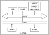
- 238000010586 diagram Methods 0.000 description 6
- 238000005516 engineering process Methods 0.000 description 5
- 238000004519 manufacturing process Methods 0.000 description 5
- 230000004044 response Effects 0.000 description 4
- 230000008859 change Effects 0.000 description 3
- 238000004891 communication Methods 0.000 description 3
- 238000011161 development Methods 0.000 description 3
- 230000008569 process Effects 0.000 description 3
- 238000012545 processing Methods 0.000 description 3
- 230000003068 static effect Effects 0.000 description 3
- 238000004458 analytical method Methods 0.000 description 2
- 238000006243 chemical reaction Methods 0.000 description 2
- 230000005284 excitation Effects 0.000 description 2
- 230000010354 integration Effects 0.000 description 2
- OKTJSMMVPCPJKN-UHFFFAOYSA-N Carbon Chemical compound [C] OKTJSMMVPCPJKN-UHFFFAOYSA-N 0.000 description 1
- 241000278713 Theora Species 0.000 description 1
- 230000015572 biosynthetic process Effects 0.000 description 1
- 238000004364 calculation method Methods 0.000 description 1
- 230000001413 cellular effect Effects 0.000 description 1
- 230000007547 defect Effects 0.000 description 1
- 229910021389 graphene Inorganic materials 0.000 description 1
- 239000004973 liquid crystal related substance Substances 0.000 description 1
- 230000007257 malfunction Effects 0.000 description 1
- 238000012986 modification Methods 0.000 description 1
- 230000004048 modification Effects 0.000 description 1
- 230000003287 optical effect Effects 0.000 description 1
- 239000004065 semiconductor Substances 0.000 description 1
- 238000003786 synthesis reaction Methods 0.000 description 1
Images


Landscapes
- Tests Of Electronic Circuits (AREA)
Abstract
本申请涉及一种FPGA多芯片的并行测试方法、装置、计算机设备、存储介质和计算机程序产品。该方法包括:通过位于第一测试板至少两个测试位的被测FPGA芯片通过对应的管脚接收ATE测试系统测试通道的功能测试信号,根据测试信号对各被测FPGA芯片的被测功能模块并行进行功能测试,得到至少两个FPGA芯片的功能测试结果,位于第二测试板的被测FPGA芯片通过对应的管脚接收ATE测试系统测试通道的测试信号,根据测试信号进行电性能测试,得到FPGA芯片的电性能测试结果。该方法解耦了FPGA芯片的功能测试和电性能测试,通过并行进行功能测试,解决了多管脚FPGA芯片测试需求与ATE机台测试通道有限的矛盾,缩短测试时间,提高FPGA芯片的测试效率,实现批量芯片的快速测试。

The application relates to a parallel testing method, device, computer equipment, storage medium and computer program product of FPGA multi-chips. The method comprises: receiving the functional test signal of the test channel of the ATE test system through the corresponding pins of the tested FPGA chip located at least two test positions on the first test board, and testing the tested functional modules of each tested FPGA chip according to the test signal Carry out function test in parallel, obtain the function test result of at least two FPGA chips, be positioned at the FPGA chip under test of the second test board to receive the test signal of ATE test system test channel through corresponding pin, carry out electrical performance test according to test signal, obtain The electrical performance test results of the FPGA chip. This method decouples the functional test and electrical performance test of the FPGA chip, and solves the contradiction between the multi-pin FPGA chip test requirements and the limited test channels of the ATE machine by performing functional tests in parallel, shortens the test time, and improves the test efficiency of the FPGA chip , to achieve rapid testing of batch chips.
Description
技术领域technical field
本申请涉及芯片测试技术领域,特别是涉及一种FPGA多芯片的并行测试方法、装置和计算机设备存储介质和计算机程序产品。The present application relates to the technical field of chip testing, in particular to a FPGA multi-chip parallel testing method, device, computer equipment storage medium and computer program product.
背景技术Background technique
现场可编程门阵列FPGA芯片(field programmable gate array,FPGA)具有逻辑密度高、可重复配置、在线编程等优点。伴随半导体制造工艺技术的不断进步,FPGA向着高速、大容量、高密度、多功能的方向快速发展,内部资源规模达到千万门级甚至亿门级,芯片管脚数量从几百提升到1000pin以上。A field programmable gate array (FPGA) chip (field programmable gate array, FPGA) has the advantages of high logic density, repeatable configuration, and online programming. With the continuous advancement of semiconductor manufacturing technology, FPGA is developing rapidly towards high speed, large capacity, high density, and multi-function. The scale of internal resources has reached tens of millions or even hundreds of millions of gates, and the number of chip pins has increased from a few hundred to more than 1,000 pins. .
芯片测试是保证FPGA产品质量的重要途径,随着FPGA芯片集成规模不断增大,芯片管脚数量越来越多。同时随着国产FPGA芯片市场规模和应用需求的增加,单一型号量产规模已达到几万到几十万片,芯片量产测试需求量激增,对FPGA的高效快速测试提出了需求。近年来,基于ATE(Auto test equipment)自动化测试系统的FPGA芯片测试方法以其测试效率高、测试速度快成为批量化FPGA芯片测试的主流技术。Chip testing is an important way to ensure the quality of FPGA products. As the integration scale of FPGA chips continues to increase, the number of chip pins is increasing. At the same time, with the increase of domestic FPGA chip market size and application demand, the mass production scale of a single model has reached tens of thousands to hundreds of thousands of pieces, and the demand for chip mass production testing has surged, which puts forward the demand for efficient and fast testing of FPGA. In recent years, the FPGA chip testing method based on the ATE (Auto test equipment) automated test system has become the mainstream technology for batch FPGA chip testing due to its high test efficiency and fast test speed.
目前,目前大规模先进FPGA芯片管脚数达到1000pin以上,芯片的测试需求量大,而现有的集成电路ATE测试机台通道数一般不超过2000。ATE测试系统由于测试通道资源的限制,对于千级数量管脚的FPGA芯片,现有ATE测试机台只能进行单芯片测试。对于大容量、高密度、高速的FPGA芯片,数字处理器DSP、锁相环PLL、数字时钟管理单元DCM、控制器、高速接口等内部功能模块复杂,测试向量规模大,单颗芯片的测试时间可达10min以上,测试成本高,严重影响量产芯片规模测试。因此,对于大规模千级数量管脚FPGA芯片,存在芯片测试时间长,测试成本高和测试效率低的问题,严重影响量产芯片的规模测试。At present, the number of pins of large-scale advanced FPGA chips has reached more than 1,000 pins, and the demand for chip testing is large, while the number of channels of existing integrated circuit ATE test machines generally does not exceed 2,000. ATE test system Due to the limitation of test channel resources, for FPGA chips with thousands of pins, existing ATE test machines can only perform single-chip tests. For large-capacity, high-density, high-speed FPGA chips, internal functional modules such as digital processor DSP, phase-locked loop PLL, digital clock management unit DCM, controller, and high-speed interface are complex, the scale of test vectors is large, and the test time of a single chip It can reach more than 10 minutes, and the test cost is high, which seriously affects the scale test of mass-produced chips. Therefore, for large-scale FPGA chips with thousands of pins, there are problems of long chip test time, high test cost and low test efficiency, which seriously affect the scale test of mass-produced chips.
发明内容Contents of the invention
基于此,有必要针对上述技术问题,提供一种利用ATE测试系统实现大规模千级数量管脚FPGA多芯片的并行测试的方法、装置、计算机设备和计算机可读存储介质,提高测试效率,减少测试时间和成本。Based on this, it is necessary to address the above-mentioned technical problems to provide a method, device, computer equipment and computer-readable storage medium for utilizing an ATE test system to realize parallel testing of a large-scale thousand-level quantity pin FPGA multi-chip, improve test efficiency, and reduce Test time and cost.
第一方面,本申请提供了一种利用ATE测试系统进行千级数量管脚FPGA多芯片的并行测试方法。所述方法包括:In a first aspect, the present application provides a method for parallel testing of FPGA multi-chips with thousands of pins by using an ATE test system. The methods include:
位于第一测试板至少两个测试位的被测FPGA芯片通过对应的管脚接收ATE测试系统测试通道的功能测试信号,根据所述时钟信号对各所述被测FPGA芯片的被测功能模块并行进行功能测试,得到至少两个所述FPGA芯片的功能测试结果;The FPGA chip under test that is positioned at at least two test positions on the first test board receives the functional test signal of the ATE test system test channel through the corresponding pin, and parallelizes the tested functional modules of each of the FPGA chips under test according to the clock signal Carry out functional test, obtain the functional test result of at least two described FPGA chips;
位于第二测试板的所述被测FPGA芯片通过对应的管脚接收ATE测试系统测试通道的测试信号,根据所述测试信号进行电性能测试,得到所述FPGA芯片的电性能测试结果。The FPGA chip under test on the second test board receives the test signal of the test channel of the ATE test system through the corresponding pin, performs an electrical performance test according to the test signal, and obtains the electrical performance test result of the FPGA chip.
在其中一个实施例中,所述位于第一测试板的被测FPGA芯片通过对应的管脚接收ATE测试系统测试通道的功能测试信号,根据所述测试信号对各所述被测FPGA芯片的被测功能模块进行功能测试,得到所述FPGA芯片的功能测试结果,包括:In one of the embodiments, the FPGA chip under test on the first test board receives the functional test signal of the test channel of the ATE test system through the corresponding pin, and the tested FPGA chip of each FPGA chip under test is tested according to the test signal. Test function module to carry out functional test, obtain the functional test result of described FPGA chip, comprise:
位于第一测试板的被测FPGA芯片通过对应的管脚接收ATE测试系统测试通道的时钟信号;The measured FPGA chip located on the first test board receives the clock signal of the ATE test system test channel through the corresponding pin;
根据所述时钟信号,FPGA芯片内建自测试向量生成模块生成测试向量;According to the clock signal, the FPGA chip built-in self-test vector generation module generates test vectors;
将所述测试向量作用于FPGA芯片的被测功能模块,得到实际输出;Applying the test vector to the tested functional module of the FPGA chip to obtain actual output;
比较测试向量的期望输出和所述实际输出,得到所述FPGA芯片的被测功能模块的测试结果;Comparing the expected output of the test vector and the actual output, obtain the test result of the tested functional module of the FPGA chip;
根据各所述被测功能模块的测试结果,得到所述FPGA芯片的功能测试结果。According to the test results of each of the tested functional modules, the functional test results of the FPGA chip are obtained.
在其中一个实施例中,所述第二测试板包括一个测试位;所述电性能检测所需的测试通道的数量大于所述功能性能测试所需的测试通道的数量,接近ATE测试系统的测试通道数。In one of the embodiments, the second test board includes a test position; the number of test channels required for the electrical performance detection is greater than the number of test channels required for the functional performance test, which is close to the test of the ATE test system number of channels.
在其中一个实施例中,所述方法还包括:In one embodiment, the method also includes:
获取所述被测FPGA芯片在所述第一测试板的不同测试位的被测功能模块的测试结果;Obtain the test results of the tested functional modules of the FPGA chip under test in different test positions of the first test board;
若所述被测FPGA芯片在不同测试位的被测功能模块的测试结果合格,则验证所述FPGA芯片的所述被测功能模块的测试通过。If the test results of the tested functional modules of the tested FPGA chip in different test positions are qualified, then verify that the test of the tested functional modules of the FPGA chip passes.
在其中一个实施例中,所述测试通道预先根据管脚定义配置,所述配置包括电源配置、IO配置、电压/电流配置和时序配置。In one of the embodiments, the test channel is configured in advance according to pin definition, and the configuration includes power configuration, IO configuration, voltage/current configuration and timing configuration.
在其中一个实施例中,所述第一测试板包括四个测试位;四个被测FPGA芯片被同时放置在所述测试位上并行进行功能测试。In one of the embodiments, the first test board includes four test positions; four FPGA chips to be tested are placed on the test positions at the same time for functional testing in parallel.
第二方面,本申请还提供了一种FPGA多芯片的并行测试装置。所述装置包括:In the second aspect, the present application also provides a parallel testing device for FPGA multi-chips. The devices include:
功能测试模块,位于第一测试板至少两个测试位的被测FPGA芯片用于通过对应的管脚接收ATE测试系统测试通道的功能测试信号,根据所述测试信号对各所述被测FPGA芯片的被测功能模块并行进行功能测试,得到至少两个所述FPGA芯片的功能能测试结果;Functional test module, the FPGA chip under test at least two test positions on the first test board is used to receive the functional test signal of the ATE test system test channel through the corresponding pin, and each described FPGA chip under test according to the test signal The tested functional modules are functionally tested in parallel to obtain functional performance test results of at least two FPGA chips;
电性能测试模块,位于第二测试板的所述被测FPGA芯片用于通过对应的管脚接收ATE测试系统测试通道的测试信号,根据所述测试信号进行电性能测试,得到所述FPGA芯片的电性能测试结果。Electrical performance test module, the described measured FPGA chip that is positioned at the second test board is used for receiving the test signal of ATE test system test channel by corresponding pin, carries out electrical performance test according to described test signal, obtains the described FPGA chip Electrical performance test results.
第三方面,本申请还提供了一种计算机设备。所述计算机设备包括存储器和处理器,所述存储器存储有计算机程序,所述处理器执行所述计算机程序时实现以下步骤:In a third aspect, the present application also provides a computer device. The computer device includes a memory and a processor, the memory stores a computer program, and the processor implements the following steps when executing the computer program:
位于第一测试板至少两个测试位的被测FPGA芯片通过对应的管脚接收ATE测试系统测试通道的功能测试信号,根据所述测试信号对各所述被测FPGA芯片的被测功能模块并行进行功能测试,得到至少两个所述FPGA芯片的功能测试结果;The FPGA chip under test at least two test positions on the first test board receives the functional test signal of the ATE test system test channel through the corresponding pin, and parallels the tested functional modules of each of the FPGA chips under test according to the test signal Carry out functional test, obtain the functional test result of at least two described FPGA chips;
位于第二测试板的所述被测FPGA芯片通过对应的管脚接收ATE测试系统测试通道的测试信号,根据所述测试信号进行电性能测试,得到所述FPGA芯片的电性能测试结果。The FPGA chip under test on the second test board receives the test signal of the test channel of the ATE test system through the corresponding pin, performs an electrical performance test according to the test signal, and obtains the electrical performance test result of the FPGA chip.
第四方面,本申请还提供了一种计算机可读存储介质。所述计算机可读存储介质,其上存储有计算机程序,所述计算机程序被处理器执行时实现以下步骤:In a fourth aspect, the present application also provides a computer-readable storage medium. The computer-readable storage medium has a computer program stored thereon, and when the computer program is executed by a processor, the following steps are implemented:
位于第一测试板至少两个测试位的被测FPGA芯片通过对应的管脚接收ATE测试系统测试通道的功能测试信号,根据所述测试信号对各所述被测FPGA芯片的被测功能模块并行进行功能测试,得到所述FPGA芯片的功能测试结果;The FPGA chip under test at least two test positions on the first test board receives the functional test signal of the ATE test system test channel through the corresponding pin, and parallels the tested functional modules of each of the FPGA chips under test according to the test signal Carry out functional test, obtain the functional test result of described FPGA chip;
位于第二测试板的所述被测FPGA芯片通过对应的管脚接收ATE测试系统测试通道的测试信号,根据所述测试信号进行电性能测试,得到所述FPGA芯片的电性能测试结果。The FPGA chip under test on the second test board receives the test signal of the test channel of the ATE test system through the corresponding pin, performs an electrical performance test according to the test signal, and obtains the electrical performance test result of the FPGA chip.
第五方面,本申请还提供了一种计算机程序产品。所述计算机程序产品,包括计算机程序,该计算机程序被处理器执行时实现以下步骤:In a fifth aspect, the present application also provides a computer program product. The computer program product includes a computer program, and when the computer program is executed by a processor, the following steps are implemented:
位于第一测试板至少两个测试位的被测FPGA芯片通过对应的管脚接收ATE测试系统测试通道的功能测试信号,根据所述功能测试信号对各所述被测FPGA芯片的被测功能模块并行进行功能测试,得到至少两个所述FPGA芯片的功能测试结果;The FPGA chip under test that is positioned at at least two test positions of the first test board receives the functional test signal of the ATE test system test channel through the corresponding pin, and the tested functional modules of each described FPGA chip under test are tested according to the functional test signal. Carry out functional test in parallel, obtain the functional test result of at least two described FPGA chips;
位于第二测试板的所述被测FPGA芯片通过对应的管脚接收ATE测试系统测试通道的测试信号,根据所述测试信号进行电性能测试,得到所述FPGA芯片的电性能测试结果。The FPGA chip under test on the second test board receives the test signal of the test channel of the ATE test system through the corresponding pin, performs an electrical performance test according to the test signal, and obtains the electrical performance test result of the FPGA chip.
上述FPGA多芯片的并行测试方法、装置、计算机设备和存储介质,通过位于第一测试板至少两个测试位的被测FPGA芯片通过对应的管脚接收ATE测试系统测试通道的功能测试信号,根据测试信号对各被测FPGA芯片的被测功能模块并行进行功能测试,得到至少两个FPGA芯片的功能测试结果,位于第二测试板的被测FPGA芯片通过对应的管脚接收ATE测试系统测试通道的测试信号,根据测试信号进行电性能测试,得到FPGA芯片的电性能测试结果。该方法解耦了FPGA芯片的功能测试和电性能测试,通过并行进行功能测试,解决了多管脚FPGA芯片测试需求与ATE机台测试通道有限的矛盾,缩短测试时间,提高FPGA芯片的测试效率,实现批量芯片的快速测试。The above-mentioned FPGA multi-chip parallel testing method, device, computer equipment and storage medium receive the functional test signal of the ATE test system test channel by the FPGA chip under test at least two test positions on the first test board through corresponding pins, according to The test signal performs a functional test on the tested functional modules of each tested FPGA chip in parallel, and obtains the functional test results of at least two FPGA chips. The tested FPGA chip located on the second test board receives the test channel of the ATE test system through the corresponding pin According to the test signal, the electrical performance test is performed according to the test signal, and the electrical performance test result of the FPGA chip is obtained. This method decouples the functional test and electrical performance test of the FPGA chip, and solves the contradiction between the multi-pin FPGA chip test requirements and the limited test channels of the ATE machine by performing functional tests in parallel, shortens the test time, and improves the test efficiency of the FPGA chip , to achieve rapid testing of batch chips.
附图说明Description of drawings
图1为一个实施例中FPGA多芯片的并行测试方法的流程示意图;Fig. 1 is the schematic flow sheet of the parallel testing method of FPGA multi-chip in an embodiment;
图2为一个实施例中FPGA芯片内部功能模块BIST测试原理的示意图;Fig. 2 is the schematic diagram of FPGA chip internal function module BIST test principle in an embodiment;
图3为一个实施例中单芯片全pin测试的设计示意图;Fig. 3 is the design schematic diagram of the full pin test of single chip in an embodiment;
图4为一个实施例中FPGA多芯片并行地进行功能测试的设计示意图;Fig. 4 is the design schematic diagram that FPGA multi-chip carries out function test in parallel in one embodiment;
图5为一个实施例中FPGA多芯片的并行测试装置的结构框图;Fig. 5 is the structural block diagram of the parallel testing device of FPGA multi-chip in an embodiment;
图6为一个实施例中计算机设备的内部结构图。Figure 6 is an internal block diagram of a computer device in one embodiment.
具体实施方式Detailed ways
为了使本申请的目的、技术方案及优点更加清楚明白,以下结合附图及实施例,对本申请进行进一步详细说明。应当理解,此处描述的具体实施例仅用以解释本申请,并不用于限定本申请。In order to make the purpose, technical solution and advantages of the present application clearer, the present application will be further described in detail below in conjunction with the accompanying drawings and embodiments. It should be understood that the specific embodiments described here are only used to explain the present application, not to limit the present application.
本申请的FPGA多芯片的并行测试方法,可通过ATE(Auto test equipment)自动化测试系统实现。ATE自动化测试系统进行芯片配置,提供电源、时钟等功能测试信号,位于第一测试板至少两个测试位的被测FPGA芯片通过对应的管脚接收ATE测试系统测试通道的功能测试信号,根据测试信号对各被测FPGA芯片的被测功能模块并行进行功能测试,得到至少两个FPGA芯片的功能测试结果,位于第二测试板的被测FPGA芯片通过对应的ATE测试系统管脚接收测试通道的测试信号,根据测试信号进行电性能测试,得到FPGA芯片的电性能测试结果。该方法根据测试IO数量需求和测试时间,划分FPGA芯片功能性能测试项目,采用多芯片有效pin并行测试设计进行FPGA功能测试,采用单芯片全pin测试设计进行FPGA电性能参数全测试,形成一种覆盖FPGA功能性能全测试需求的且测试效率较高的测试方法。The FPGA multi-chip parallel testing method of the present application can be realized by an ATE (Auto test equipment) automated testing system. The ATE automated test system configures the chip and provides functional test signals such as power supply and clock. The FPGA chip under test located at least two test positions on the first test board receives the functional test signal of the ATE test system test channel through the corresponding pins. According to the test The signal is used to perform functional tests on the tested functional modules of each tested FPGA chip in parallel to obtain the functional test results of at least two FPGA chips. The tested FPGA chip located on the second test board receives the test channel through the corresponding ATE test system pin The test signal is used to perform an electrical performance test according to the test signal to obtain an electrical performance test result of the FPGA chip. This method divides the FPGA chip functional performance test items according to the test IO quantity requirements and test time, adopts multi-chip effective pin parallel test design for FPGA functional test, and adopts single-chip full pin test design for FPGA electrical performance parameter full test, forming a A test method that covers the full test requirements of FPGA functional performance and has high test efficiency.
在一个实施例中,如图1所示,提供一种FPGA多芯片的并行测试方法,该方法应用于ATE自动化测试系统,包括以下步骤:In one embodiment, as shown in Figure 1, a kind of parallel testing method of FPGA multi-chip is provided, and this method is applied to ATE automated test system, comprises the following steps:
步骤102,位于第一测试板至少两个测试位的被测FPGA芯片通过对应的管脚接收ATE测试系统测试通道的功能测试信号,根据测试信号对各所述被测FPGA芯片的被测功能模块并行进行功能测试,得到至少两个FPGA芯片的功能测试结果。Step 102, the FPGA chip under test at least two test positions on the first test board receives the functional test signal of the ATE test system test channel through the corresponding pin, and performs a test on each functional module of the FPGA chip under test according to the test signal Perform functional tests in parallel to obtain functional test results of at least two FPGA chips.
其中,现场可编程门阵列FPGA芯片(field programmable gate array,FPGA)具有逻辑密度高、可重复配置、在线编程等优点,在硬件系统完成开发以至实际使用后,还可重新编程配置更改系统设计,同时还具有设计开发周期短、成本较低等优点。目前,FPGA向着高速、大容量、高密度、多功能的方向快速发展,内部资源规模达到千万门级甚至亿门级,芯片管脚数量从几百提升到1000pin以上。Among them, the field programmable gate array (FPGA) chip has the advantages of high logic density, repeatable configuration, and online programming. After the hardware system is developed and actually used, it can be reprogrammed to change the system design. At the same time, it also has the advantages of short design and development cycle and low cost. At present, FPGA is developing rapidly in the direction of high speed, large capacity, high density, and multi-function. The scale of internal resources has reached tens of millions or even hundreds of millions of gates, and the number of chip pins has increased from a few hundred to more than 1,000 pins.
芯片测试是保证FPGA产品质量的重要途径,随着FPGA芯片集成规模不断增大,芯片管脚数量越来越多。同时随着国产FPGA芯片市场规模和应用需求的增加,单一型号量产规模已达到几万到几十万片,芯片量产测试需求量激增,对FPGA的高效快速测试提出了需求。ATE自动化测试系统的FPGA芯片测试方法以其测试效率高、测试速度快成为批量化FPGA芯片测试的主流技术。Chip testing is an important way to ensure the quality of FPGA products. As the integration scale of FPGA chips continues to increase, the number of chip pins is increasing. At the same time, with the increase of domestic FPGA chip market size and application demand, the mass production scale of a single model has reached tens of thousands to hundreds of thousands of pieces, and the demand for chip mass production testing has surged, which puts forward the demand for efficient and fast testing of FPGA. The FPGA chip testing method of the ATE automated test system has become the mainstream technology for batch FPGA chip testing due to its high test efficiency and fast test speed.
功能性能测试是FPGA芯片测试的重点测试内容,具有测试向量规模大、测试时间长但所需ATE测试通道数少的特点。根据FPGA芯片所有资源可以独立配置且重复编程的特性,采用内建自测试的方法,利用芯片内部可编程逻辑资源构建测试向量生成、施加、输出分析的测试控制结构,使用相对较少的时钟、向量、输出等有效pin,即可实现FPGA芯片硬核功能模块和基本电路功能模块的功能性能测试。即,FPGA芯片进行功能性能测试需要较少的测试通道,第一测试板可以有至少两个测试位,至少两颗FPGA芯片可以同时进行功能性能测试。其中,功能性能测试主要包括APM、GTX、BRAM、PLL、DCM、SCAN、CLB、IOB、配置模块等硬核功能电路模块和基本电路模块的功能性能测试。Functional performance test is the key test content of FPGA chip test, which has the characteristics of large test vector scale, long test time but few required ATE test channels. According to the characteristics that all resources of the FPGA chip can be independently configured and reprogrammed, the built-in self-test method is adopted to use the internal programmable logic resources of the chip to build a test control structure for test vector generation, application, and output analysis, using relatively few clocks, Effective pins such as vector and output can realize the functional performance test of the FPGA chip hard core function module and the basic circuit function module. That is, the functional performance test of the FPGA chip requires fewer test channels, the first test board can have at least two test positions, and at least two FPGA chips can perform the functional performance test at the same time. Among them, functional performance testing mainly includes functional performance testing of APM, GTX, BRAM, PLL, DCM, SCAN, CLB, IOB, configuration modules and other hard-core functional circuit modules and basic circuit modules.
其中,ATE测试系统有两种测试板,分别为ATE测试系统第一测试板和ATE测试系统第二测试板。ATE测试系统第一测试板对FPGA芯片进行功能测试。具体地,ATE自动化测试系统通过测试通道给出功能测试信号,被测FPGA芯片通过对应的管脚接收测试信号,测试信号作用于被测功能模块以进行功能测试,得到FPGA芯片的功能测试结果。由于功能测试具有测试时间长、需要ATE测试通道数量少的特点,第一测试板上可以有至少两个测试位,放置于至少两个测试位的被测FPGA芯片并行进行功能测试。Wherein, the ATE test system has two test boards, which are the first test board of the ATE test system and the second test board of the ATE test system. The first test board of the ATE test system performs functional tests on the FPGA chip. Specifically, the ATE automated test system provides a functional test signal through the test channel, and the FPGA chip under test receives the test signal through the corresponding pin, and the test signal acts on the functional module under test for functional testing, and obtains the functional test result of the FPGA chip. Since the functional test has the characteristics of a long test time and a small number of ATE test channels, there may be at least two test positions on the first test board, and the tested FPGA chips placed in at least two test positions perform functional tests in parallel.
步骤104,位于第二测试板的被测FPGA芯片通过对应的管脚接收ATE测试系统测试通道的测试信号,根据测试信号进行电性能测试,得到FPGA芯片的电性能测试结果。Step 104, the FPGA chip under test on the second test board receives the test signal of the test channel of the ATE test system through the corresponding pin, conducts the electrical performance test according to the test signal, and obtains the electrical performance test result of the FPGA chip.
其中,ATE测试系统有两种测试板,分别为ATE测试系统第一测试板和ATE测试系统第二测试板。ATE测试系统第一测试板对FPGA芯片进行功能测试,ATE测试系统第二测试板对FPGA芯片进行电性能测试。电性能参数测试的测试具有时间短、需要ATE测试通道数多的特点。Wherein, the ATE test system has two test boards, which are the first test board of the ATE test system and the second test board of the ATE test system. The first test board of the ATE test system performs a functional test on the FPGA chip, and the second test board of the ATE test system performs an electrical performance test on the FPGA chip. The test of the electrical performance parameter test has the characteristics of short time and a large number of ATE test channels.
具体地,ATE自动化测试系统通过测试通道给出测试信号,被测FPGA芯片通过对应的管脚接收测试信号,根据测试信号进行电性能测试,得到FPGA芯片的电性能测试结果。Specifically, the ATE automated test system provides a test signal through the test channel, and the FPGA chip under test receives the test signal through the corresponding pin, performs an electrical performance test according to the test signal, and obtains the electrical performance test result of the FPGA chip.
上述FPGA多芯片的并行测试方法,通过位于第一测试板至少两个测试位的被测FPGA芯片通过对应的管脚接收ATE测试系统测试通道的功能测试信号,根据测试信号对各被测FPGA芯片的被测功能模块并行进行功能测试,得到至少两个FPGA芯片的功能测试结果,位于第二测试板的被测FPGA芯片通过对应的管脚接收ATE测试系统测试通道的测试信号,根据测试信号进行电性能测试,得到FPGA芯片的电性能测试结果。该方法解耦了FPGA芯片的功能测试和电性能测试,通过并行进行功能测试,解决了多管脚FPGA芯片测试需求与ATE机台测试通道有限的矛盾,缩短测试时间,提高FPGA芯片的测试效率,实现批量芯片的快速测试。The above-mentioned FPGA multi-chip parallel testing method, receives the functional test signal of the ATE test system test channel by the FPGA chip under test at least two test positions on the first test board through the corresponding pins, and tests each FPGA chip under test according to the test signal The tested functional modules are tested in parallel to obtain the functional test results of at least two FPGA chips. The tested FPGA chip located on the second test board receives the test signal of the ATE test system test channel through the corresponding pin, and performs the test according to the test signal. Electrical performance test, to obtain the electrical performance test results of the FPGA chip. This method decouples the functional test and electrical performance test of the FPGA chip, and solves the contradiction between the multi-pin FPGA chip test requirements and the limited test channels of the ATE machine by performing functional tests in parallel, shortens the test time, and improves the test efficiency of the FPGA chip , to achieve rapid testing of batch chips.
在另一个实施例中,位于第一测试板的被测FPGA芯片通过对应的管脚接收ATE测试系统测试通道的功能测试信号,根据测试信号对被测功能模块并行功能性能测试,得到FPGA芯片的功能测试结果,包括:位于第一测试板的被测FPGA芯片通过对应的管脚接收ATE测试系统测试通道的时钟信号;根据时钟信号,FPGA芯片内建自测试向量生成模块生成测试向量;将测试向量作用于FPGA芯片的被测功能模块,得到实际输出;比较测试向量的期望输出和实际输出,得到FPGA芯片的被测功能模块的测试结果;根据各被测功能模块的测试结果,得到FPGA芯片的功能测试结果。In another embodiment, the FPGA chip under test on the first test board receives the functional test signal of the test channel of the ATE test system through the corresponding pin, and performs a parallel functional performance test on the tested functional module according to the test signal to obtain the FPGA chip. Functional test results, including: the FPGA chip under test on the first test board receives the clock signal of the ATE test system test channel through the corresponding pin; according to the clock signal, the FPGA chip built-in self-test vector generation module generates test vectors; The vector acts on the tested functional module of the FPGA chip to obtain the actual output; compare the expected output and the actual output of the test vector to obtain the test result of the tested functional module of the FPGA chip; according to the test results of each tested functional module, the FPGA chip is obtained The functional test results.
ATE自动化测试系统对FPGA芯片进行测试的流程如下:利用向量转换工具将FPGA芯片配置程序转化成ATE机台可以识别的测试向量,进而通过ATE机台向被测FPGA加载测试向量,ATE机台同时提供被测FPGA芯片运行所需电源和时钟等信号,使FPGA芯片处于特定工作状态,进而根据FPGA芯片输出,来判断测试项是否合格。The process of testing the FPGA chip by the ATE automated test system is as follows: use the vector conversion tool to convert the FPGA chip configuration program into a test vector that can be recognized by the ATE machine, and then load the test vector to the FPGA under test through the ATE machine, and the ATE machine simultaneously Provide the signals such as power supply and clock required for the operation of the FPGA chip under test, so that the FPGA chip is in a specific working state, and then judge whether the test item is qualified according to the output of the FPGA chip.
其中,通过FPGA测试开发工具进行功能BIST测试设计并经过编译、综合等过程后生成配置码流,如Xilinx FPGA开发工具Vivado生成的.bit格式文件。采用EDA工具以及ATE自带转换工具,将芯片配置码流转换成ATE测试机台可以识别的Pattern测试向量文件,如Advantest 93000测试机台的binl文件。也可以按照FPGA芯片功能、电性能参数测试需求,采用ATE测试系统自带的测试程序开发工具进行测试程序开发。Among them, the functional BIST test design is carried out through the FPGA test development tool, and the configuration code stream is generated after compilation and synthesis, such as the .bit format file generated by the Xilinx FPGA development tool Vivado. Use EDA tools and ATE conversion tools to convert the chip configuration code stream into a pattern test vector file that can be recognized by the ATE test machine, such as the binl file of the Advantest 93000 test machine. It is also possible to use the test program development tool that comes with the ATE test system for test program development according to the FPGA chip function and electrical performance parameter test requirements.
大规模高性能FPGA芯片主要由可编程逻辑单元(CLB)、可编程输入输出单元(IOB)、可编程互连资源(IR)、典型功能硬核模块,如块随机存取存储器(BRAM)、时钟管理器(DCM)、算术处理模块(APM)、高速串行模块(GTX)、边界扫描模块(SCAN)、配置模块等构成。其中,内建自测试设计将逻辑资源分为三个模块:测试向量生成模块(TPG)、输出响应检验电路模块(ORA)和被测功能模块(DUT)。FPGA芯片内部功能模块BIST测试原理如图2所示。内建自测试(BIST)设计技术通过在芯片的设计中加入一些额外的自测试电路,测试时只需要从外部施加必要的控制信号,通过运行内建的自测试硬件和软件,检查被测电路的缺陷或故障。TPG模块是根据不同DUT模块的功能来进行编写的,在ATE自动化测试系统给出的时钟信号激励下,TPG模块产生被测模块的激励、控制以及所有输入组合等测试向量,DUT模块接收测试向量后,产生实际响应数据。在测试向量输入条件下,TPG模块产生被测模块产生的预期数据。ORA模块接收实际响应数据和预期数据,并将实际响应数据与预期数据进行比较,判定DUT模块的功能是否正确,并将判定结果pass/fail输出。Large-scale high-performance FPGA chip is mainly composed of programmable logic unit (CLB), programmable input and output unit (IOB), programmable interconnect resources (IR), typical functional hard core modules, such as block random access memory (BRAM), Clock manager (DCM), arithmetic processing module (APM), high-speed serial module (GTX), boundary scan module (SCAN), configuration module, etc. Among them, the built-in self-test design divides logic resources into three modules: test pattern generation module (TPG), output response verification circuit module (ORA) and function module under test (DUT). The BIST test principle of the internal functional module of the FPGA chip is shown in Figure 2. The built-in self-test (BIST) design technology adds some additional self-test circuits to the design of the chip, and only needs to apply the necessary control signals from the outside to check the circuit under test by running the built-in self-test hardware and software. defects or malfunctions. The TPG module is written according to the functions of different DUT modules. Under the excitation of the clock signal given by the ATE automated test system, the TPG module generates test vectors such as the excitation, control and all input combinations of the tested module, and the DUT module receives the test vectors. After that, the actual response data is generated. Under the test vector input condition, the TPG module produces the expected data produced by the module under test. The ORA module receives the actual response data and the expected data, compares the actual response data with the expected data, judges whether the function of the DUT module is correct, and outputs the judgment result pass/fail.
在本实施例中,在解耦功能测试和电性能测试的基础上,对FPGA芯片进行功能性能测试来判断FPGA芯片的质量。In this embodiment, on the basis of the decoupling function test and the electrical performance test, a functional performance test is performed on the FPGA chip to judge the quality of the FPGA chip.
在一个实施例中,第二测试板包括一个测试位;电性能检测所需的测试通道的数量大于功能测试所需的测试通道的数量,接近ATE测试系统的测试通道数。In one embodiment, the second test board includes a test position; the number of test channels required for electrical performance testing is greater than the number of test channels required for functional testing, and is close to the number of test channels of the ATE test system.
其中,电性能参数测试项主要包括短路/开路、输入高/低电平电压、输出高/低电平电压、输出高/低电平电流、引脚上/下拉电流、漏电流等。Among them, the electrical performance parameter test items mainly include short circuit/open circuit, input high/low level voltage, output high/low level voltage, output high/low level current, pin pull-up/pull-down current, leakage current, etc.
电性能参数,特别是输入输出电参数需要对FPGA芯片所有IO管脚进行测试,因而对于pin数多的FPGA芯片,电性能参数测试需要的ATE测试通道数多,因此,对于电性能测试采用单芯片全pin的方式进行测试。除此之外,相对于测试复杂、测试向量规范大的FPGA芯片功能性能测试,FPGA芯片的电性能参数测试的时间较短,在FPGA芯片的总测试时间中占比较低。Electrical performance parameters, especially input and output electrical parameters, need to test all IO pins of the FPGA chip. Therefore, for an FPGA chip with a large number of pins, the electrical performance parameter test requires a large number of ATE test channels. Therefore, a single The chip is tested in a full-pin manner. In addition, compared with the functional performance test of FPGA chips with complex tests and large test vector specifications, the test time of electrical performance parameters of FPGA chips is shorter, and the proportion of the total test time of FPGA chips is relatively low.
图3为单芯片全pin测试的设计,如图3所示,FPGA芯片单芯片全pin的ATE测试板上只有1个FPGA芯片测试Socket,每个测试Socket是一个测试位,将FPGA芯片的所有管脚Pin连接到ATE机台相应的测试通道,进行FPGA芯片电性能参数的全覆盖测试。Figure 3 shows the design of the single-chip full-pin test. As shown in Figure 3, there is only one FPGA chip test Socket on the FPGA chip single-chip full-pin ATE test board, and each test Socket is a test bit. The pin Pin is connected to the corresponding test channel of the ATE machine, and the full coverage test of the electrical performance parameters of the FPGA chip is performed.
在本实施例中,通过ATE测试系统第二测试板将电性能测试和功能测试分开,为并行地进行功能测试提供条件。In this embodiment, the electrical performance test and the functional test are separated through the second test board of the ATE test system, so as to provide conditions for performing functional tests in parallel.
在另一个实施例中,该方法还包括:获取被测FPGA芯片在第一测试板的不同测试位的被测功能模块的测试结果;若被测FPGA芯片在不同测试位的被测功能模块的测试结果合格,则验证FPGA芯片的被测功能模块的测试通过。In another embodiment, the method also includes: obtaining the test results of the tested functional modules of the FPGA chip under test in different test positions of the first test board; If the test result is qualified, it is verified that the test of the tested functional module of the FPGA chip is passed.
具体地,ATE测试系统第一测试板上至少有两个FPGA芯片测试Socket,每个测试Socket是一个测试位,将同一颗FPGA芯片分别放置在ATE测试系统第一测试板上的不同测试位进行功能测试,如果不同测试位的测试结果相同,则一致性验证通过。一致性验证通过表明ATE测试系统第一测试板上的不同测试位是相同的,没有差异的。Specifically, there are at least two FPGA chip test Sockets on the first test board of the ATE test system, each test Socket is a test position, and the same FPGA chip is respectively placed on different test positions on the first test board of the ATE test system Functional test, if the test results of different test bits are the same, the consistency verification is passed. The passing of the consistency verification indicates that the different test bits on the first test board of the ATE test system are the same and there is no difference.
在本实施例中,通过一致性验证来考察ATE测试系统第一测试板上的不同测试位是否有差别,通过ATE测试系统第一测试板上的不同测试位的结果相同,即一致性验证通过,来保证芯片检测结果的一致性和准确性。In this embodiment, check whether the different test bits on the first test board of the ATE test system are different through consistency verification, and the results of different test bits on the first test board of the ATE test system are the same, that is, the consistency verification is passed , to ensure the consistency and accuracy of chip detection results.
在另一个实施例中,测试通道预先根据管脚定义配置,配置包括电源配置、IO(输入、输出)配置、电压/电流配置和时序配置中的至少一种。In another embodiment, the test channel is pre-configured according to pin definitions, and the configuration includes at least one of power configuration, IO (input, output) configuration, voltage/current configuration and timing configuration.
其中电源配置包括:电源正负极性、负载电容、电源板卡、测试位、对应的电源通道等。IO配置包括:IO通道类型(输入、输出)、测试模式、阻抗、测试板卡、测试位、对应的测试通道等。电压/电流配置包括:芯片管脚名称、类型、输入电压下限、输入电压上限,输出电压下限、输出电压上限,电压/电流配置是通过ATE测试机台确定施加在FPGA芯片管脚上的驱动电压/电流、输出电压/电流。时序配置包括:时序参数名、参数模型、时序波形、频率等,时序配置是通过ATE测试机台确定施加在FPGA芯片管脚上信号时序波形参数。The power supply configuration includes: positive and negative polarity of the power supply, load capacitance, power board, test bit, corresponding power channel, etc. IO configuration includes: IO channel type (input, output), test mode, impedance, test board, test bit, corresponding test channel, etc. Voltage/current configuration includes: chip pin name, type, input voltage lower limit, input voltage upper limit, output voltage lower limit, output voltage upper limit, voltage/current configuration is to determine the driving voltage applied to FPGA chip pins through ATE testing machine /current, output voltage/current. The timing configuration includes: timing parameter name, parameter model, timing waveform, frequency, etc. The timing configuration is to determine the timing waveform parameters of the signal applied to the pins of the FPGA chip through the ATE test machine.
在定义好FPGA芯片的管脚后,使用ATE测试机台的编程工具,对FPGA芯片进行测试通道配置。After defining the pins of the FPGA chip, use the programming tool of the ATE test machine to configure the test channel for the FPGA chip.
在本实施例中,FPGA芯片进行测试通道配置后,通过软件将测试通道和芯片管脚相连,以便进行后续的功能测试和电性能测试。In this embodiment, after the test channel is configured on the FPGA chip, the test channel is connected to the pins of the chip through software, so as to perform subsequent functional tests and electrical performance tests.
在一个实施例中,第一测试板包括四个测试位;四个被测FPGA芯片被同时放置在所述测试位上并行进行功能测试。In one embodiment, the first test board includes four test positions; four FPGA chips to be tested are simultaneously placed on the test positions to perform functional tests in parallel.
与常规的集成电路相比,FPGA的ATE测试在实现电性能参数测试基础上,需要重点对FPGA芯片内部基本电路模块、硬核电路模块的功能进行测试验证。FPGA芯片功能性能测试一般采用内建自测试BIST的方法,对外部IO的需求量较少,同时还可以采用IO复用进一步减少所需IO,因而需要的ATE测试通道数较少。由于FPGA芯片的功能性能测试项目较多,不同测试项目对ATE测试通道、测试向量规模、测试时间等测试资源需求不同,因而在FPGA测试中,可以根据实际需求按照功能性能测试项对IO需求较少、电性能参数测试项对IO需求多的总原则调整测试项目划分。Compared with conventional integrated circuits, the ATE test of FPGA needs to focus on testing and verifying the functions of the basic circuit modules and hard-core circuit modules inside the FPGA chip on the basis of realizing the electrical performance parameter test. The FPGA chip functional performance test generally adopts the built-in self-test BIST method, which requires less external IO. At the same time, IO multiplexing can be used to further reduce the required IO, so the number of ATE test channels required is small. Since there are many functional performance test items for FPGA chips, different test items have different requirements for test resources such as ATE test channels, test vector scale, and test time. The general principle of adjusting the division of test items is the general principle that there are fewer electrical performance parameter test items and more IO requirements.
以某千万门级多管脚FPGA芯片为例,该芯片的管脚数为900,选用的ATE机台具有128个电源通道、1024个数字通道,通常情况下只能同时测试1颗FPGA芯片。通过对FPGA芯片功能性能测试有效pin的测试通道需求分析,单颗FPGA芯片功能性能测试需要的ATE测试通道为:216个数字通道和17个电源通道。216个数字通道对应的是46个FPGA配置管脚、128个FPGA功能性能测试向量管脚和42个FPGA芯片时钟信号管脚。FPGA配置管脚连接到ATE测试数字通道,以将FPGA芯片配置为BIST功能。FPGA功能性能测试向量管脚连接到ATE测试数字通道,为功能性能测试提供向量输入。FPGA芯片时钟信号管脚连接到ATE测试数字通道,为功能性能测试及调试提供时钟信号。FPGA芯片的电源管脚包括内核电源VCCINT、辅助电路电源VCCAUX、块存储器VCCBRAM电源、参考电压VREF、GND等200多个供电相关管脚,但在驱动电流足够大的情况下,相同电压输入的管脚可以接入到1个ATE电源供电通道,因此FPGA电源供电使用17个ATE电源通道。因此,具有128个电源通道、1024个数字通道的ATE机台可以同时满足4颗FPGA芯片并行地进行功能性能测试。Take a 10-million-gate multi-pin FPGA chip as an example. The number of pins of this chip is 900. The selected ATE machine has 128 power channels and 1024 digital channels. Usually, only one FPGA chip can be tested at the same time. . Through the analysis of the test channel requirements for the effective pins of the FPGA chip functional performance test, the ATE test channels required for the functional performance test of a single FPGA chip are: 216 digital channels and 17 power channels. The 216 digital channels correspond to 46 FPGA configuration pins, 128 FPGA functional performance test vector pins and 42 FPGA chip clock signal pins. The FPGA configuration pins are connected to the ATE test digital channel to configure the FPGA chip for BIST function. The FPGA functional performance test vector pin is connected to the ATE test digital channel to provide vector input for the functional performance test. The FPGA chip clock signal pin is connected to the ATE test digital channel to provide a clock signal for functional performance testing and debugging. The power supply pins of the FPGA chip include more than 200 power supply related pins such as the core power supply VCCINT, the auxiliary circuit power supply VCCAUX, the block memory VCCBRAM power supply, the reference voltage VREF, and GND. pin can be connected to 1 ATE power supply channel, so the FPGA power supply uses 17 ATE power supply channels. Therefore, an ATE machine with 128 power channels and 1024 digital channels can satisfy the functional performance test of four FPGA chips in parallel.
如图4所示,根据FPGA芯片功能BIST测试向量设计所占用的FPGA芯片管脚pin,在选用的FPGA芯片ATE机台测试通道资源约束下,将ATE测试通道资源分配到多个FPGA芯片功能测试需要使用的管脚,包括电源、时钟、向量、配置、输出等,实现多个FPGA芯片有效pin与ATE测试通道的连接,ATE第一测试板上有4个FPGA芯片测试Socket,每个测试Socket是一个测试位,将功能性能测试所必须使用的电源、时钟、向量、配置等有效pin连接到ATE机台的测试通道,实现多颗芯片的并行测试。测试效率PTE可以采用以下公式计算:As shown in Figure 4, according to the FPGA chip pins occupied by the FPGA chip function BIST test vector design, under the constraints of the selected FPGA chip ATE machine test channel resources, the ATE test channel resources are allocated to multiple FPGA chip function tests The pins that need to be used, including power supply, clock, vector, configuration, output, etc., realize the connection between the effective pins of multiple FPGA chips and the ATE test channel. There are 4 FPGA chip test sockets on the first ATE test board, and each test socket It is a test bit, which connects effective pins such as power supply, clock, vector, and configuration necessary for functional performance testing to the test channel of the ATE machine to realize parallel testing of multiple chips. The test efficiency PTE can be calculated by the following formula:

式中MST1为多芯片功能测试项的并行测试时间,NS为并行测试的芯片数量,SST1为单芯片电性能参数测试项的测试时间,SST2为常规的单颗芯片完成功能、电性能参数测试项测试的总时间。In the formula, MST 1 is the parallel test time of the multi-chip function test item, NS is the number of chips tested in parallel, SST 1 is the test time of the single-chip electrical performance parameter test item, and SST 2 is the conventional single chip to complete the function and electrical performance The total time for parameter test item testing.
以某千万门级千级数量管脚的FPGA芯片为例,其功能测试项包括:APM、CRAM、DRAM、PLL、MBE存储单元故障测试、GTX、配置模块等FPGA内部功能模块测试。电性能参数测试项包括:短路/开路、输出高/低电平(覆盖CMOS 3.3V/2.5V/1.8V/1.5V/1.2V)、引脚上拉电流、引脚下拉电流、输入漏电流、静态电流等。FPGA芯片内部各模块内建自测试设计覆盖上述功能测试项。采用Advantest 93000ATE测试机台,实现了功能测试项的4芯片并行地进行功能性能测试和电性能参数测试项的单芯片串行测试。通过在4个测试位分别进行相同FPGA芯片的功能测试验证,功能测试结果相同,验证了多芯片并行测试的一致性。功能测试项和电性能参数测试项的测试所需时间如表1所示。Taking an FPGA chip with tens of millions of gates and thousands of pins as an example, its functional test items include: APM, CRAM, DRAM, PLL, MBE storage unit fault test, GTX, configuration module and other FPGA internal functional module tests. Electrical performance parameter test items include: short circuit/open circuit, output high/low level (covering CMOS 3.3V/2.5V/1.8V/1.5V/1.2V), pin pull-up current, pin pull-down current, input leakage current , Static current, etc. The built-in self-test design of each module inside the FPGA chip covers the above functional test items. Using the Advantest 93000ATE test machine, the functional performance test of the four chips of the functional test item and the single-chip serial test of the electrical performance parameter test item are realized. Through the functional test verification of the same FPGA chip at the four test positions, the functional test results are the same, which verifies the consistency of the multi-chip parallel test. Table 1 shows the test time required for functional test items and electrical performance parameter test items.
表1功能测试时间Table 1 Functional test time

采用4芯片并行地进行功能测试与单芯片全pin电性能参数测试的方法,测试4颗FPGA芯片的时间为56.794s,显著缩短了测试时间,测试效率为3.31,即相比ATE测试机台只能进行单芯片测试,测试效率提升到3倍多。在此基础上,进一步优化多芯片有效pin功能测试设计,增加同时测试的芯片数量,将会进一步提升测试效率。Using 4 chips in parallel for functional testing and single-chip full-pin electrical performance parameter testing, the test time for 4 FPGA chips is 56.794s, which significantly shortens the test time, and the test efficiency is 3.31, that is, compared with the ATE test machine, only It can perform single-chip testing, and the testing efficiency is increased by more than 3 times. On this basis, further optimizing the multi-chip effective pin function test design and increasing the number of chips tested at the same time will further improve the test efficiency.
在本实施例中,芯片功能测试采用的内建自测试BIST方法进行,只需要较少的ATE测试通道,因此,ATE测试系统第一测试板上可以并行地进行至少两颗芯片的测试,从而提高FPGA芯片的测试效率,缩短测试时间,实现批量芯片的快速测试。In this embodiment, the built-in self-test BIST method that the chip function test adopts is carried out, only need less ATE test channels, therefore, the test of at least two chips can be carried out in parallel on the first test board of the ATE test system, thereby Improve the test efficiency of FPGA chips, shorten the test time, and realize the rapid test of batch chips.
应该理解的是,虽然上述的各实施例涉及的流程图中的各个步骤按照箭头的指示依次显示,但是这些步骤并不是必然按照箭头指示的顺序依次执行。除非本文中有明确的说明,这些步骤的执行并没有严格的顺序限制,这些步骤可以以其它的顺序执行。而且,上述的各实施例涉及的流程图中的至少一部分步骤可以包括多个步骤或者多个阶段,这些步骤或者阶段并不必然是在同一时刻执行完成,而是可以在不同的时刻执行,这些步骤或者阶段的执行顺序也不必是依次进行,而是可以与其它步骤或者其它步骤中的步骤或者阶段的至少一部分轮流或者交替地执行。It should be understood that although the steps in the flow charts involved in the above embodiments are displayed in sequence according to the arrows, these steps are not necessarily executed in sequence in the order indicated by the arrows. Unless otherwise specified herein, there is no strict order restriction on the execution of these steps, and these steps can be executed in other orders. Moreover, at least some of the steps in the flowcharts involved in the above embodiments may include multiple steps or stages, and these steps or stages are not necessarily executed at the same time, but may be executed at different times. The execution order of the steps or stages does not have to be performed sequentially, but may be performed alternately or alternately with other steps or at least a part of steps or stages in other steps.
基于同样的发明构思,本申请还提供了一种用于实现上述所涉及的FPGA多芯片的并行测试装置。该装置所提供的解决问题的实现方案与上述方法中所记载的实现方案相似,故下面所提供的一个或多个FPGA多芯片的并行测试装置实施例中的具体限定可以参见上文中对于FPGA多芯片的并行测试方法的限定,在此不再赘述。Based on the same inventive concept, the present application also provides a parallel testing device for realizing the FPGA multi-chip involved above. The implementation scheme provided by the device to solve the problem is similar to the implementation scheme described in the above-mentioned method, so the specific limitations in the parallel test device embodiment of one or more FPGA multichips provided below can refer to the above for FPGA multichip The limitation of the chip parallel testing method will not be repeated here.
在一个实施例中,如图5所示,提供了一种FPGA多芯片的并行测试装置500,包括:功能性能测试模块502和电性能测试模块504,其中:In one embodiment, as shown in Figure 5, a kind of FPGA multi-chip parallel testing device 500 is provided, comprising: functional
功能测试模块502,位于第一测试板至少两个测试位的被测FPGA芯片用于通过对应的管脚接收ATE测试系统测试通道的功能测试信号,根据测试信号对各所述被测FPGA芯片的被测功能模块并行进行功能测试,得到至少两个FPGA芯片的功能性能测试结果;
电性能测试模块504,位于ATE测试系统第二测试板的被测FPGA芯片用于通过对应的管脚接收测试通道的测试信号,根据测试信号进行电性能测试,得到FPGA芯片的电性能测试结果。Electrical
在另一个实施例中,功能测试模块,位于第一测试板的被测FPGA芯片用于通过对应的管脚接收ATE测试系统测试通道的功能测试信号,根据测试信号对被测功能模块进行功能测试,得到FPGA芯片的功能测试结果,包括:位于第一测试板的被测FPGA芯片通过对应的管脚接收ATE测试系统测试通道的时钟信号;根据时钟信号,FPGA芯片内建自测试向量生成模块生成测试向量;将测试向量作用于FPGA芯片的被测功能模块,得到实际输出;比较测试向量的期望输出和实际输出,得到FPGA芯片的被测功能模块的测试结果;根据各被测功能模块的测试结果,得到FPGA芯片的功能测试结果。In another embodiment, the function test module, the FPGA chip under test located on the first test board is used to receive the function test signal of the test channel of the ATE test system through the corresponding pin, and perform the function test on the function module under test according to the test signal , to obtain the functional test results of the FPGA chip, including: the FPGA chip under test located on the first test board receives the clock signal of the test channel of the ATE test system through the corresponding pin; according to the clock signal, the FPGA chip built-in self-test vector generation module generates Test vector; apply the test vector to the tested functional module of the FPGA chip to obtain the actual output; compare the expected output and actual output of the test vector to obtain the test result of the tested functional module of the FPGA chip; according to the test of each tested functional module As a result, the functional test results of the FPGA chip are obtained.
在另一个实施例中,第二测试板包括一个测试位;电性能检测所需的测试通道的数量大于功能性能测试所需的测试通道的数量,接近ATE测试系统的测试通道数。In another embodiment, the second test board includes a test position; the number of test channels required for electrical performance testing is greater than the number of test channels required for functional performance testing, and is close to the number of test channels of the ATE test system.
在另一个实施例中,一种FPGA多芯片的并行测试装置还包括:一致性验证模块;In another embodiment, a parallel testing device of FPGA multi-chip also includes: a consistency verification module;
一致性验证模块,用于获取被测FPGA芯片在第一测试板的不同测试位的被测功能模块的测试结果;若被测FPGA芯片在不同测试位的被测功能模块的测试结果合格,则验证FPGA芯片的被测功能模块的测试通过。The consistency verification module is used to obtain the test results of the tested functional modules of the FPGA chip under test in different test positions of the first test board; if the test results of the tested functional modules of the tested FPGA chip in different test positions are qualified, then Verify that the test of the tested functional module of the FPGA chip passes.
在另一个实施例中,测试通道预先根据管脚定义配置,配置包括电源配置、IO配置、电压/电流配置和时序配置。In another embodiment, the test channel is pre-configured according to the pin definition, and the configuration includes power configuration, IO configuration, voltage/current configuration and timing configuration.
在另一个实施例中,第一测试板包括四个测试位;四个被测FPGA芯片被同时放置在测试位上并行进行功能测试。In another embodiment, the first test board includes four test positions; four tested FPGA chips are placed on the test positions at the same time for functional testing in parallel.
上述FPGA多芯片的并行测试装置中的各个模块可全部或部分通过软件、硬件及其组合来实现。上述各模块可以硬件形式内嵌于或独立于计算机设备中的处理器中,也可以以软件形式存储于计算机设备中的存储器中,以便于处理器调用执行以上各个模块对应的操作。Each module in the above-mentioned FPGA multi-chip parallel testing device can be fully or partially realized by software, hardware and combinations thereof. The above-mentioned modules can be embedded in or independent of the processor in the computer device in the form of hardware, and can also be stored in the memory of the computer device in the form of software, so that the processor can invoke and execute the corresponding operations of the above-mentioned modules.
在一个实施例中,提供了一种计算机设备,该计算机设备可以是控制器,其内部结构图可以如图6所示。该计算机设备包括通过系统总线连接的处理器、存储器、通信接口和显示屏。其中,该计算机设备的处理器用于提供计算和控制能力。该计算机设备的存储器包括非易失性存储介质、内存储器。该非易失性存储介质存储有操作系统和计算机程序。该内存储器为非易失性存储介质中的操作系统和计算机程序的运行提供环境。该计算机设备的通信接口用于与外部的终端进行有线或无线方式的通信,无线方式可通过WIFI、移动蜂窝网络、NFC(近场通信)或其他技术实现。该计算机程序被处理器执行时以实现一种FPGA多芯片的并行测试方法。该计算机设备的显示屏可以是液晶显示屏或电子墨水显示屏。In one embodiment, a computer device is provided. The computer device may be a controller, and its internal structure may be as shown in FIG. 6 . The computer device includes a processor, a memory, a communication interface and a display screen connected by a system bus. Wherein, the processor of the computer device is used to provide calculation and control capabilities. The memory of the computer device includes a non-volatile storage medium and an internal memory. The non-volatile storage medium stores an operating system and computer programs. The internal memory provides an environment for the operation of the operating system and computer programs in the non-volatile storage medium. The communication interface of the computer device is used to communicate with an external terminal in a wired or wireless manner, and the wireless manner can be realized through WIFI, mobile cellular network, NFC (Near Field Communication) or other technologies. When the computer program is executed by the processor, a method for parallel testing of FPGA multi-chips is realized. The display screen of the computer device may be a liquid crystal display screen or an electronic ink display screen.
本领域技术人员可以理解,图6中示出的结构,仅仅是与本申请方案相关的部分结构的框图,并不构成对本申请方案所应用于其上的计算机设备的限定,具体的计算机设备可以包括比图中所示更多或更少的部件,或者组合某些部件,或者具有不同的部件布置。Those skilled in the art can understand that the structure shown in FIG. 6 is only a block diagram of a part of the structure related to the solution of this application, and does not constitute a limitation on the computer equipment to which the solution of this application is applied. The specific computer equipment can be More or fewer components than shown in the figures may be included, or some components may be combined, or have a different arrangement of components.
在一个实施例中,提供了一种计算机设备,包括存储器和处理器,存储器中存储有计算机程序,该处理器执行计算机程序时实现以下步骤:In one embodiment, a computer device is provided, including a memory and a processor, a computer program is stored in the memory, and the processor implements the following steps when executing the computer program:
位于第一测试板的至少两个测试位被测FPGA芯片通过对应的管脚接收ATE测试系统测试通道的功能测试信号,根据测试信号对各所述被测FPGA芯片的被测功能模块并行进行功能测试,得到至少两个FPGA芯片的功能测试结果;The FPGA chip under test of at least two test positions on the first test board receives the functional test signal of the ATE test system test channel through the corresponding pin, and performs functions in parallel according to the test signal to the tested functional modules of each described FPGA chip under test. Test, obtain the functional test results of at least two FPGA chips;
位于第二测试板的被测FPGA芯片通过对应的管脚接收ATE测试系统测试通道的测试信号,根据测试信号进行电性能测试,得到FPGA芯片的电性能测试结果。The tested FPGA chip located on the second test board receives the test signal of the test channel of the ATE test system through the corresponding pin, conducts the electrical performance test according to the test signal, and obtains the electrical performance test result of the FPGA chip.
在其中一个实施例中,位于第一测试板的被测FPGA芯片通过对应的管脚接收ATE测试系测试通道的时钟信号,根据时钟信号对被测功能模块进行功能测试,得到FPGA芯片的功能测试结果,包括:In one of the embodiments, the FPGA chip under test on the first test board receives the clock signal of the test channel of the ATE test system through the corresponding pins, and performs a functional test on the functional module under test according to the clock signal to obtain the functional test of the FPGA chip. Results, including:
位于第一测试板的被测FPGA芯片通过对应的管脚接收ATE测试系统测试通道的时钟信号;The measured FPGA chip located on the first test board receives the clock signal of the ATE test system test channel through the corresponding pin;
根据时钟信号,FPGA芯片内建自测试向量生成模块生成测试向量;According to the clock signal, the FPGA chip built-in self-test vector generation module generates test vectors;
将测试向量作用于FPGA芯片的被测功能模块,得到实际输出;Apply the test vector to the tested functional module of the FPGA chip to obtain the actual output;
比较测试向量的期望输出和实际输出,得到FPGA芯片的被测功能模块的测试结果;Compare the expected output and actual output of the test vector to obtain the test result of the tested functional module of the FPGA chip;
根据各被测功能模块的测试结果,得到FPGA芯片的功能测试结果。According to the test results of each tested functional module, the functional test results of the FPGA chip are obtained.
在其中一个实施例中,第二测试板包括一个测试位;电性能检测所需的测试通道的数量大于功能性能测试所需的测试通道的数量,接近ATE测试系统的测试通道数。In one of the embodiments, the second test board includes a test position; the number of test channels required for electrical performance testing is greater than the number of test channels required for functional performance testing, and is close to the number of test channels of the ATE test system.
在其中一个实施例中,方法还包括:In one embodiment, the method also includes:
获取被测FPGA芯片在第一测试板的不同测试位的被测功能模块的测试结果;Obtain the test results of the tested functional modules of the tested FPGA chip in different test positions of the first test board;
若被测FPGA芯片在不同测试位的被测功能模块的测试结果合格,则验证FPGA芯片的被测功能模块的测试通过。If the test results of the tested functional modules of the tested FPGA chip at different test positions are qualified, it is verified that the test of the tested functional modules of the FPGA chip passes.
在其中一个实施例中,测试通道预先根据管脚定义配置,配置包括电源配置、IO配置、电压/电流配置和时序配置。In one embodiment, the test channel is pre-configured according to the pin definition, and the configuration includes power configuration, IO configuration, voltage/current configuration and timing configuration.
在一个实施例中,第一测试板包括四个测试位;四个被测FPGA芯片被同时放置在测试位上并行进行功能测试。In one embodiment, the first test board includes four test positions; four FPGA chips to be tested are simultaneously placed on the test positions for functional testing in parallel.
在一个实施例中,提供了一种计算机可读存储介质,其上存储有计算机程序,计算机程序被处理器执行时实现以下步骤:In one embodiment, a computer-readable storage medium is provided, on which a computer program is stored, and when the computer program is executed by a processor, the following steps are implemented:
位于第一测试板至少两个测试位的被测FPGA芯片通过对应的管脚接收ATE测试系统测试通道的功能测试信号,根据测试信号对各所述被测FPGA芯片的被测功能模块并行进行功能测试,得到至少两个FPGA芯片的功能测试结果;The FPGA chips under test at least two test positions on the first test board receive the functional test signals of the ATE test system test channel through corresponding pins, and perform functions in parallel on the tested functional modules of each of the FPGA chips under test according to the test signals. Test, obtain the functional test results of at least two FPGA chips;
位于第二测试板的被测FPGA芯片通过对应的管脚接收ATE测试系统测试通道的测试信号,根据测试信号进行电性能测试,得到FPGA芯片的电性能测试结果。The tested FPGA chip located on the second test board receives the test signal of the test channel of the ATE test system through the corresponding pin, conducts the electrical performance test according to the test signal, and obtains the electrical performance test result of the FPGA chip.
在其中一个实施例中,位于第一测试板至少两个测试位的被测FPGA芯片通过对应的管脚接收ATE测试系统测试通道的功能测试信号,根据测试信号对各所述被测FPGA芯片的被测功能模块并行进行功能测试,得到至少两个FPGA芯片的功能测试结果,包括:In one of the embodiments, the FPGA chip under test at least two test positions on the first test board receives the functional test signal of the ATE test system test channel through the corresponding pin, and the FPGA chip under test is tested according to the test signal. The functional modules under test are tested in parallel to obtain the functional test results of at least two FPGA chips, including:
位于第一测试板的被测FPGA芯片通过对应的管脚接收ATE测试系统测试通道的时钟信号;The measured FPGA chip located on the first test board receives the clock signal of the ATE test system test channel through the corresponding pin;
根据时钟信号,FPGA芯片内建自测试向量生成模块生成测试向量;According to the clock signal, the FPGA chip built-in self-test vector generation module generates test vectors;
将测试向量作用于FPGA芯片的被测功能模块,得到实际输出;Apply the test vector to the tested functional module of the FPGA chip to obtain the actual output;
比较测试向量的期望输出和实际输出,得到FPGA芯片的被测功能模块的测试结果;Compare the expected output and actual output of the test vector to obtain the test result of the tested functional module of the FPGA chip;
根据各被测功能模块的测试结果,得到FPGA芯片的功能性能测试结果。According to the test results of each tested functional module, the functional performance test results of the FPGA chip are obtained.
在其中一个实施例中,第二测试板包括一个测试位;电性能检测所需的测试通道的数量大于功能性能测试所需的测试通道的数量。In one embodiment, the second test board includes a test position; the number of test channels required for electrical performance testing is greater than the number of test channels required for functional performance testing.
在其中一个实施例中,方法还包括:In one embodiment, the method also includes:
获取被测FPGA芯片在第一测试板的不同测试位的被测功能模块的测试结果;Obtain the test results of the tested functional modules of the tested FPGA chip in different test positions of the first test board;
若被测FPGA芯片在不同测试位的被测功能模块的测试结果合格,则验证FPGA芯片的被测功能模块的测试通过。If the test results of the tested functional modules of the tested FPGA chip at different test positions are qualified, it is verified that the test of the tested functional modules of the FPGA chip passes.
在其中一个实施例中,测试通道预先根据管脚定义配置,配置包括电源配置、IO配置、电压/电流配置和时序配置。In one embodiment, the test channel is pre-configured according to the pin definition, and the configuration includes power configuration, IO configuration, voltage/current configuration and timing configuration.
在一个实施例中,第一测试板包括四个测试位;四个被测FPGA芯片被同时放置在测试位上并行进行功能测试。In one embodiment, the first test board includes four test positions; four FPGA chips to be tested are simultaneously placed on the test positions for functional testing in parallel.
本领域普通技术人员可以理解实现上述实施例的方法中的全部或部分流程,是可以通过计算机程序来指令相关的硬件来完成,的计算机程序可存储于一非易失性计算机可读取存储介质中,该计算机程序在执行时,可包括如上述各方法的实施例的流程。其中,本申请所提供的各实施例中所使用的对存储器、数据库或其它介质的任何引用,均可包括非易失性和易失性存储器中的至少一种。非易失性存储器可包括只读存储器(Read-OnlyMemory,ROM)、磁带、软盘、闪存、光存储器、高密度嵌入式非易失性存储器、阻变存储器(ReRAM)、磁变存储器(Magnetoresistive Random Access Memory,MRAM)、铁电存储器(Ferroelectric Random Access Memory,FRAM)、相变存储器(Phase Change Memory,PCM)、石墨烯存储器等。易失性存储器可包括随机存取存储器(Random Access Memory,RAM)或外部高速缓冲存储器等。作为说明而非局限,RAM可以是多种形式,比如静态随机存取存储器(Static Random Access Memory,SRAM)或动态随机存取存储器(Dynamic RandomAccess Memory,DRAM)等。本申请所提供的各实施例中所涉及的数据库可包括关系型数据库和非关系型数据库中至少一种。非关系型数据库可包括基于区块链的分布式数据库等,不限于此。本申请所提供的各实施例中所涉及的处理器可为通用处理器、中央处理器、图形处理器、数字信号处理器、可编程逻辑器、基于量子计算的数据处理逻辑器等,不限于此。Those of ordinary skill in the art can understand that all or part of the processes in the methods of the above embodiments can be completed through computer programs to instruct related hardware, and the computer programs can be stored in a non-volatile computer-readable storage medium In this case, when the computer program is executed, it may include the processes of the embodiments of the above-mentioned methods. Wherein, any reference to storage, database or other media used in the various embodiments provided in the present application may include at least one of non-volatile and volatile storage. Non-volatile memory can include read-only memory (Read-Only Memory, ROM), magnetic tape, floppy disk, flash memory, optical memory, high-density embedded non-volatile memory, resistive variable memory (ReRAM), magnetic variable memory (Magnetoresistive Random Access Memory, MRAM), Ferroelectric Random Access Memory (FRAM), Phase Change Memory (Phase Change Memory, PCM), graphene memory, etc. The volatile memory may include random access memory (Random Access Memory, RAM) or external cache memory. As an illustration and not a limitation, the RAM can be in various forms, such as static random access memory (Static Random Access Memory, SRAM) or dynamic random access memory (Dynamic Random Access Memory, DRAM). The databases involved in the various embodiments provided in this application may include at least one of a relational database and a non-relational database. The non-relational database may include a blockchain-based distributed database, etc., but is not limited thereto. The processors involved in the various embodiments provided by this application can be general-purpose processors, central processing units, graphics processors, digital signal processors, programmable logic devices, data processing logic devices based on quantum computing, etc., and are not limited to this.
以上实施例的各技术特征可以进行任意的组合,为使描述简洁,未对上述实施例中的各技术特征所有可能的组合都进行描述,然而,只要这些技术特征的组合不存在矛盾,都应当认为是本说明书记载的范围。The technical features of the above embodiments can be combined arbitrarily. To make the description concise, all possible combinations of the technical features in the above embodiments are not described. However, as long as there is no contradiction in the combination of these technical features, they should be It is considered to be within the range described in this specification.
以上实施例仅表达了本申请的几种实施方式,其描述较为具体和详细,但并不能因此而理解为对本申请专利范围的限制。应当指出的是,对于本领域的普通技术人员来说,在不脱离本申请构思的前提下,还可以做出若干变形和改进,这些都属于本申请的保护范围。因此,本申请的保护范围应以所附权利要求为准。The above examples only express several implementation modes of the present application, and the description thereof is relatively specific and detailed, but should not be construed as limiting the patent scope of the present application. It should be noted that those skilled in the art can make several modifications and improvements without departing from the concept of the present application, and these all belong to the protection scope of the present application. Therefore, the protection scope of the present application should be determined by the appended claims.
Claims (10)
Priority Applications (1)
| Application Number | Priority Date | Filing Date | Title |
|---|---|---|---|
| CN202211260839.XA CN115656769A (en) | 2022-10-14 | 2022-10-14 | FPGA multi-chip parallel test method, device and computer equipment |
Applications Claiming Priority (1)
| Application Number | Priority Date | Filing Date | Title |
|---|---|---|---|
| CN202211260839.XA CN115656769A (en) | 2022-10-14 | 2022-10-14 | FPGA multi-chip parallel test method, device and computer equipment |
Publications (1)
| Publication Number | Publication Date |
|---|---|
| CN115656769A true CN115656769A (en) | 2023-01-31 |
Family
ID=84987879
Family Applications (1)
| Application Number | Title | Priority Date | Filing Date |
|---|---|---|---|
| CN202211260839.XA Pending CN115656769A (en) | 2022-10-14 | 2022-10-14 | FPGA multi-chip parallel test method, device and computer equipment |
Country Status (1)
| Country | Link |
|---|---|
| CN (1) | CN115656769A (en) |
Cited By (3)
| Publication number | Priority date | Publication date | Assignee | Title |
|---|---|---|---|---|
| CN116359715A (en) * | 2023-05-26 | 2023-06-30 | 南京芯驰半导体科技有限公司 | Multi-chip testing method and device, electronic equipment and storage medium |
| CN117540674A (en) * | 2024-01-09 | 2024-02-09 | 南京宏泰半导体科技股份有限公司 | Chip test system and test method for integrated audio and video system |
| CN118837726A (en) * | 2024-09-20 | 2024-10-25 | 绍兴圆方半导体有限公司 | MEMS chip testing method and system and storage medium |
-
2022
- 2022-10-14 CN CN202211260839.XA patent/CN115656769A/en active Pending
Cited By (5)
| Publication number | Priority date | Publication date | Assignee | Title |
|---|---|---|---|---|
| CN116359715A (en) * | 2023-05-26 | 2023-06-30 | 南京芯驰半导体科技有限公司 | Multi-chip testing method and device, electronic equipment and storage medium |
| CN116359715B (en) * | 2023-05-26 | 2023-11-03 | 南京芯驰半导体科技有限公司 | Multi-chip testing method and device, electronic equipment and storage medium |
| CN117540674A (en) * | 2024-01-09 | 2024-02-09 | 南京宏泰半导体科技股份有限公司 | Chip test system and test method for integrated audio and video system |
| CN117540674B (en) * | 2024-01-09 | 2024-04-05 | 南京宏泰半导体科技股份有限公司 | Chip test system and test method for integrated audio and video system |
| CN118837726A (en) * | 2024-09-20 | 2024-10-25 | 绍兴圆方半导体有限公司 | MEMS chip testing method and system and storage medium |
Similar Documents
| Publication | Publication Date | Title |
|---|---|---|
| CN115656769A (en) | FPGA multi-chip parallel test method, device and computer equipment | |
| US10281524B2 (en) | Test partition external input/output interface control for test partitions in a semiconductor | |
| US8650524B1 (en) | Method and apparatus for low-pin count testing of integrated circuits | |
| US20140078841A1 (en) | Programmable memory built in self repair circuit | |
| CN100399473C (en) | Built-in self-test system and method | |
| US8904256B1 (en) | Method and apparatus for low-pin count testing of integrated circuits | |
| CN104361909B (en) | RAM build-in self-test methods and circuit on a kind of piece | |
| CN106816178B (en) | A built-in self-test design method for multiple embedded memories on a single chip | |
| US7502267B2 (en) | Clock frequency doubler method and apparatus for serial flash testing | |
| US9835680B2 (en) | Method, device and computer program product for circuit testing | |
| CN101923133A (en) | System and method for testing wiring faults between cores of integrated circuit system on chip | |
| CN100559510C (en) | Semiconductor integrated circuit device | |
| WO2021179601A1 (en) | Method for testing control chip and related device | |
| CN106291313B (en) | Method and apparatus for testing integrated circuits | |
| US10969433B1 (en) | Method to compress responses of automatic test pattern generation (ATPG) vectors into an on-chip multiple-input shift register (MISR) | |
| US11662383B2 (en) | High-speed functional protocol based test and debug | |
| US9098486B1 (en) | Methods and apparatus for testing multiple clock domain memories | |
| CN202120623U (en) | Embedded static random access memory (SRAM) testing structure based on institute of electrical and electronic engineers (IEEE) 1500 | |
| Lee et al. | A low-cost concurrent TSV test architecture with lossless test output compression scheme | |
| Sridhar et al. | Built-in self-repair (BISR) technique widely Used to repair embedded random access memories (RAMs) | |
| CN110853696B (en) | Wafer acceptance test module and method for static memory function detection | |
| Aswin et al. | Implementation and Validation of Memory Built in Self Test (MBIST)–Survey | |
| US12112818B2 (en) | Scan chain compression for testing memory of a system on a chip | |
| Huang et al. | PLL-assisted timing circuit for accurate TSV leakage binning | |
| Kumari et al. | FPGA implementation of memory design and testing |
Legal Events
| Date | Code | Title | Description |
|---|---|---|---|
| PB01 | Publication | ||
| PB01 | Publication | ||
| SE01 | Entry into force of request for substantive examination | ||
| SE01 | Entry into force of request for substantive examination |