CN115241278A - Semiconductor device and electronic apparatus - Google Patents
Semiconductor device and electronic apparatus Download PDFInfo
- Publication number
- CN115241278A CN115241278A CN202210804923.7A CN202210804923A CN115241278A CN 115241278 A CN115241278 A CN 115241278A CN 202210804923 A CN202210804923 A CN 202210804923A CN 115241278 A CN115241278 A CN 115241278A
- Authority
- CN
- China
- Prior art keywords
- semiconductor device
- layer
- metal
- active layer
- doping
- Prior art date
- Legal status (The legal status is an assumption and is not a legal conclusion. Google has not performed a legal analysis and makes no representation as to the accuracy of the status listed.)
- Granted
Links
Images


Classifications
-
- H—ELECTRICITY
- H10—SEMICONDUCTOR DEVICES; ELECTRIC SOLID-STATE DEVICES NOT OTHERWISE PROVIDED FOR
- H10D—INORGANIC ELECTRIC SEMICONDUCTOR DEVICES
- H10D62/00—Semiconductor bodies, or regions thereof, of devices having potential barriers
- H10D62/80—Semiconductor bodies, or regions thereof, of devices having potential barriers characterised by the materials
- H10D62/83—Semiconductor bodies, or regions thereof, of devices having potential barriers characterised by the materials being Group IV materials, e.g. B-doped Si or undoped Ge
-
- G—PHYSICS
- G02—OPTICS
- G02F—OPTICAL DEVICES OR ARRANGEMENTS FOR THE CONTROL OF LIGHT BY MODIFICATION OF THE OPTICAL PROPERTIES OF THE MEDIA OF THE ELEMENTS INVOLVED THEREIN; NON-LINEAR OPTICS; FREQUENCY-CHANGING OF LIGHT; OPTICAL LOGIC ELEMENTS; OPTICAL ANALOGUE/DIGITAL CONVERTERS
- G02F1/00—Devices or arrangements for the control of the intensity, colour, phase, polarisation or direction of light arriving from an independent light source, e.g. switching, gating or modulating; Non-linear optics
- G02F1/01—Devices or arrangements for the control of the intensity, colour, phase, polarisation or direction of light arriving from an independent light source, e.g. switching, gating or modulating; Non-linear optics for the control of the intensity, phase, polarisation or colour
- G02F1/13—Devices or arrangements for the control of the intensity, colour, phase, polarisation or direction of light arriving from an independent light source, e.g. switching, gating or modulating; Non-linear optics for the control of the intensity, phase, polarisation or colour based on liquid crystals, e.g. single liquid crystal display cells
- G02F1/133—Constructional arrangements; Operation of liquid crystal cells; Circuit arrangements
- G02F1/136—Liquid crystal cells structurally associated with a semi-conducting layer or substrate, e.g. cells forming part of an integrated circuit
- G02F1/1362—Active matrix addressed cells
- G02F1/1368—Active matrix addressed cells in which the switching element is a three-electrode device
- G02F1/13685—Top gates
-
- H—ELECTRICITY
- H10—SEMICONDUCTOR DEVICES; ELECTRIC SOLID-STATE DEVICES NOT OTHERWISE PROVIDED FOR
- H10D—INORGANIC ELECTRIC SEMICONDUCTOR DEVICES
- H10D30/00—Field-effect transistors [FET]
- H10D30/01—Manufacture or treatment
- H10D30/021—Manufacture or treatment of FETs having insulated gates [IGFET]
- H10D30/031—Manufacture or treatment of FETs having insulated gates [IGFET] of thin-film transistors [TFT]
- H10D30/0312—Manufacture or treatment of FETs having insulated gates [IGFET] of thin-film transistors [TFT] characterised by the gate electrodes
- H10D30/0314—Manufacture or treatment of FETs having insulated gates [IGFET] of thin-film transistors [TFT] characterised by the gate electrodes of lateral top-gate TFTs comprising only a single gate
-
- H—ELECTRICITY
- H10—SEMICONDUCTOR DEVICES; ELECTRIC SOLID-STATE DEVICES NOT OTHERWISE PROVIDED FOR
- H10D—INORGANIC ELECTRIC SEMICONDUCTOR DEVICES
- H10D30/00—Field-effect transistors [FET]
- H10D30/01—Manufacture or treatment
- H10D30/021—Manufacture or treatment of FETs having insulated gates [IGFET]
- H10D30/031—Manufacture or treatment of FETs having insulated gates [IGFET] of thin-film transistors [TFT]
- H10D30/0321—Manufacture or treatment of FETs having insulated gates [IGFET] of thin-film transistors [TFT] comprising silicon, e.g. amorphous silicon or polysilicon
-
- H—ELECTRICITY
- H10—SEMICONDUCTOR DEVICES; ELECTRIC SOLID-STATE DEVICES NOT OTHERWISE PROVIDED FOR
- H10D—INORGANIC ELECTRIC SEMICONDUCTOR DEVICES
- H10D30/00—Field-effect transistors [FET]
- H10D30/60—Insulated-gate field-effect transistors [IGFET]
- H10D30/67—Thin-film transistors [TFT]
-
- H—ELECTRICITY
- H10—SEMICONDUCTOR DEVICES; ELECTRIC SOLID-STATE DEVICES NOT OTHERWISE PROVIDED FOR
- H10D—INORGANIC ELECTRIC SEMICONDUCTOR DEVICES
- H10D30/00—Field-effect transistors [FET]
- H10D30/60—Insulated-gate field-effect transistors [IGFET]
- H10D30/67—Thin-film transistors [TFT]
- H10D30/6729—Thin-film transistors [TFT] characterised by the electrodes
- H10D30/673—Thin-film transistors [TFT] characterised by the electrodes characterised by the shapes, relative sizes or dispositions of the gate electrodes
- H10D30/6731—Top-gate only TFTs
-
- H—ELECTRICITY
- H10—SEMICONDUCTOR DEVICES; ELECTRIC SOLID-STATE DEVICES NOT OTHERWISE PROVIDED FOR
- H10D—INORGANIC ELECTRIC SEMICONDUCTOR DEVICES
- H10D30/00—Field-effect transistors [FET]
- H10D30/60—Insulated-gate field-effect transistors [IGFET]
- H10D30/67—Thin-film transistors [TFT]
- H10D30/674—Thin-film transistors [TFT] characterised by the active materials
- H10D30/6741—Group IV materials, e.g. germanium or silicon carbide
- H10D30/6743—Silicon
- H10D30/6744—Monocrystalline silicon
-
- H—ELECTRICITY
- H10—SEMICONDUCTOR DEVICES; ELECTRIC SOLID-STATE DEVICES NOT OTHERWISE PROVIDED FOR
- H10D—INORGANIC ELECTRIC SEMICONDUCTOR DEVICES
- H10D30/00—Field-effect transistors [FET]
- H10D30/60—Insulated-gate field-effect transistors [IGFET]
- H10D30/67—Thin-film transistors [TFT]
- H10D30/674—Thin-film transistors [TFT] characterised by the active materials
- H10D30/6741—Group IV materials, e.g. germanium or silicon carbide
- H10D30/6743—Silicon
- H10D30/6745—Polycrystalline or microcrystalline silicon
-
- H—ELECTRICITY
- H10—SEMICONDUCTOR DEVICES; ELECTRIC SOLID-STATE DEVICES NOT OTHERWISE PROVIDED FOR
- H10D—INORGANIC ELECTRIC SEMICONDUCTOR DEVICES
- H10D30/00—Field-effect transistors [FET]
- H10D30/60—Insulated-gate field-effect transistors [IGFET]
- H10D30/67—Thin-film transistors [TFT]
- H10D30/6757—Thin-film transistors [TFT] characterised by the structure of the channel, e.g. transverse or longitudinal shape or doping profile
-
- H—ELECTRICITY
- H10—SEMICONDUCTOR DEVICES; ELECTRIC SOLID-STATE DEVICES NOT OTHERWISE PROVIDED FOR
- H10D—INORGANIC ELECTRIC SEMICONDUCTOR DEVICES
- H10D62/00—Semiconductor bodies, or regions thereof, of devices having potential barriers
- H10D62/10—Shapes, relative sizes or dispositions of the regions of the semiconductor bodies; Shapes of the semiconductor bodies
- H10D62/124—Shapes, relative sizes or dispositions of the regions of semiconductor bodies or of junctions between the regions
-
- H—ELECTRICITY
- H10—SEMICONDUCTOR DEVICES; ELECTRIC SOLID-STATE DEVICES NOT OTHERWISE PROVIDED FOR
- H10D—INORGANIC ELECTRIC SEMICONDUCTOR DEVICES
- H10D86/00—Integrated devices formed in or on insulating or conducting substrates, e.g. formed in silicon-on-insulator [SOI] substrates or on stainless steel or glass substrates
- H10D86/40—Integrated devices formed in or on insulating or conducting substrates, e.g. formed in silicon-on-insulator [SOI] substrates or on stainless steel or glass substrates characterised by multiple TFTs
- H10D86/421—Integrated devices formed in or on insulating or conducting substrates, e.g. formed in silicon-on-insulator [SOI] substrates or on stainless steel or glass substrates characterised by multiple TFTs having a particular composition, shape or crystalline structure of the active layer
-
- H—ELECTRICITY
- H10—SEMICONDUCTOR DEVICES; ELECTRIC SOLID-STATE DEVICES NOT OTHERWISE PROVIDED FOR
- H10D—INORGANIC ELECTRIC SEMICONDUCTOR DEVICES
- H10D86/00—Integrated devices formed in or on insulating or conducting substrates, e.g. formed in silicon-on-insulator [SOI] substrates or on stainless steel or glass substrates
- H10D86/40—Integrated devices formed in or on insulating or conducting substrates, e.g. formed in silicon-on-insulator [SOI] substrates or on stainless steel or glass substrates characterised by multiple TFTs
- H10D86/60—Integrated devices formed in or on insulating or conducting substrates, e.g. formed in silicon-on-insulator [SOI] substrates or on stainless steel or glass substrates characterised by multiple TFTs wherein the TFTs are in active matrices
-
- G—PHYSICS
- G02—OPTICS
- G02F—OPTICAL DEVICES OR ARRANGEMENTS FOR THE CONTROL OF LIGHT BY MODIFICATION OF THE OPTICAL PROPERTIES OF THE MEDIA OF THE ELEMENTS INVOLVED THEREIN; NON-LINEAR OPTICS; FREQUENCY-CHANGING OF LIGHT; OPTICAL LOGIC ELEMENTS; OPTICAL ANALOGUE/DIGITAL CONVERTERS
- G02F2202/00—Materials and properties
- G02F2202/10—Materials and properties semiconductor
- G02F2202/104—Materials and properties semiconductor poly-Si
-
- H—ELECTRICITY
- H10—SEMICONDUCTOR DEVICES; ELECTRIC SOLID-STATE DEVICES NOT OTHERWISE PROVIDED FOR
- H10K—ORGANIC ELECTRIC SOLID-STATE DEVICES
- H10K59/00—Integrated devices, or assemblies of multiple devices, comprising at least one organic light-emitting element covered by group H10K50/00
- H10K59/10—OLED displays
- H10K59/12—Active-matrix OLED [AMOLED] displays
Landscapes
- Physics & Mathematics (AREA)
- Nonlinear Science (AREA)
- Chemical & Material Sciences (AREA)
- Crystallography & Structural Chemistry (AREA)
- Engineering & Computer Science (AREA)
- Microelectronics & Electronic Packaging (AREA)
- Mathematical Physics (AREA)
- General Physics & Mathematics (AREA)
- Optics & Photonics (AREA)
- Thin Film Transistor (AREA)
- Recrystallisation Techniques (AREA)
- Electrodes Of Semiconductors (AREA)
Abstract
本申请提供一种半导体器件和电子装置;该半导体器件包括薄膜晶体管,薄膜晶体管包括衬底、缓冲层和有源层,缓冲层设置于衬底一侧,有源层设置于缓冲层远离衬底的一侧,其中,半导体器件还包括金属层,金属层设置于有源层朝向缓冲层的一侧,金属层包括至少一个金属块,且金属块与有源层的至少部分直接接触。本申请通过在有源层朝向缓冲层的一侧设置金属层,金属层包括至少一个金属块,使金属块与有源层的至少部分直接接触,则在将有源层由非晶硅转化为多晶硅时,由于金属块的催化作用,使得多晶硅中的晶粒的尺寸交大,减少了多晶硅中的晶界,提高了半导体器件的迁移率。

The application provides a semiconductor device and an electronic device; the semiconductor device includes a thin film transistor, the thin film transistor includes a substrate, a buffer layer and an active layer, the buffer layer is arranged on one side of the substrate, and the active layer is arranged on the buffer layer away from the substrate The semiconductor device further includes a metal layer, the metal layer is disposed on the side of the active layer facing the buffer layer, the metal layer includes at least one metal block, and the metal block is in direct contact with at least part of the active layer. In the present application, by disposing a metal layer on the side of the active layer facing the buffer layer, the metal layer includes at least one metal block, so that the metal block is in direct contact with at least part of the active layer, the active layer is converted from amorphous silicon to In the case of polysilicon, due to the catalytic effect of the metal block, the size of the crystal grains in the polysilicon becomes larger, which reduces the grain boundaries in the polysilicon and improves the mobility of the semiconductor device.
Description
技术领域technical field
本申请涉及显示技术领域,尤其是涉及一种半导体器件和电子装置。The present application relates to the field of display technology, in particular to a semiconductor device and an electronic device.
背景技术Background technique
随着显示技术的发展,现有显示器件对窄边框、高开口率、高亮度、高分辨率提出了越来越高的要求,因此,需要在减小薄膜晶体管的尺寸的同时,保持良好的开态电流。现有半导体器件会采用多晶硅作为有源层以提高载流子迁移率,提高开态电流。但在多晶硅的制备过程中,由于工艺的限制,导致激光退火后形成的多晶硅的晶粒尺寸较小,导致载流子迁移率较低,从而导致半导体器件的开态电流较低,无法满足需求。With the development of display technology, existing display devices put forward higher and higher requirements for narrow frame, high aperture ratio, high brightness and high resolution. Therefore, it is necessary to reduce the size of thin film transistors while maintaining good on-state current. Existing semiconductor devices use polysilicon as an active layer to improve carrier mobility and increase on-state current. However, in the preparation process of polysilicon, due to the limitation of the process, the grain size of the polysilicon formed after laser annealing is small, resulting in low carrier mobility, resulting in low on-state current of semiconductor devices, which cannot meet the demand. .
所以,现有半导体器件存在工艺限制形成的多晶硅的晶粒尺寸较小所导致的半导体器件的迁移率较低的技术问题。Therefore, the existing semiconductor devices have the technical problem that the mobility of the semiconductor devices is low due to the small grain size of the polysilicon formed by the process limitation.
发明内容SUMMARY OF THE INVENTION
本申请实施例提供一种半导体器件和电子装置,用以缓解现有半导体器件存在工艺限制形成的多晶硅的晶粒尺寸较小所导致的半导体器件的迁移率较低的技术问题。Embodiments of the present application provide a semiconductor device and an electronic device, so as to alleviate the technical problem of low mobility of the semiconductor device caused by the small grain size of polysilicon formed by process limitations in the existing semiconductor device.
本申请实施例提供一种半导体器件,该半导体器件Embodiments of the present application provide a semiconductor device, the semiconductor device
薄膜晶体管,所述薄膜晶体管包括:A thin film transistor, the thin film transistor comprising:
衬底;substrate;
缓冲层,设置于所述衬底一侧;a buffer layer, disposed on one side of the substrate;
有源层,设置于所述缓冲层远离所述衬底的一侧;an active layer, disposed on a side of the buffer layer away from the substrate;
其中,所述半导体器件还包括金属层,所述金属层设置于所述有源层朝向所述缓冲层的一侧,所述金属层包括至少一个金属块,且所述金属块与所述有源层的至少部分直接接触。Wherein, the semiconductor device further includes a metal layer, the metal layer is disposed on the side of the active layer facing the buffer layer, the metal layer includes at least one metal block, and the metal block is connected to the buffer layer. At least part of the source layer is in direct contact.
在一些实施例中,所述缓冲层在与所述有源层接触的区域设置有凹槽,所述金属块设置于所述凹槽内。In some embodiments, the buffer layer is provided with a groove in a region in contact with the active layer, and the metal block is provided in the groove.
在一些实施例中,所述金属层的材料的熔点小于1410摄氏度。In some embodiments, the melting point of the material of the metal layer is less than 1410 degrees Celsius.
在一些实施例中,所述金属层的材料包括铝、镍、镓、铟中的至少一个。In some embodiments, the material of the metal layer includes at least one of aluminum, nickel, gallium, and indium.
在一些实施例中,所述半导体器件包括多个薄膜晶体管,至少一个所述薄膜晶体管的有源层无晶界。In some embodiments, the semiconductor device includes a plurality of thin film transistors, and the active layer of at least one of the thin film transistors is free of grain boundaries.
在一些实施例中,所述薄膜晶体管的有源层包括第一晶粒,所述第一晶粒与所述金属块对应设置,所述第一晶粒的数量与所述金属块的数量相等。In some embodiments, the active layer of the thin film transistor includes first crystal grains, the first crystal grains are arranged corresponding to the metal blocks, and the number of the first crystal grains is equal to the number of the metal blocks .
在一些实施例中,述第一晶粒为圆形或者类圆形,所述第一晶粒的直径为1微米至5微米。In some embodiments, the first crystal grains are circular or quasi-circular, and the diameter of the first crystal grains is 1 to 5 microns.
在一些实施例中,所述薄膜晶体管包括多个第一晶粒,所述金属层包括阵列设置的金属块,所述第一晶粒的晶界位于相邻两个金属块之间。In some embodiments, the thin film transistor includes a plurality of first crystal grains, the metal layer includes metal blocks arranged in an array, and grain boundaries of the first crystal grains are located between two adjacent metal blocks.
在一些实施例中,所述有源层包括沟道部和位于所述沟道部两侧的第一掺杂部和第二掺杂部,所述第一掺杂部及所述第二掺杂部沿着所述沟道部之间的连线的形状与所述薄膜晶体管的第一掺杂部和第二掺杂部对应的金属块沿所述沟道部的连线的形状相同。In some embodiments, the active layer includes a channel portion and a first doping portion and a second doping portion located on both sides of the channel portion, the first doping portion and the second doping portion The shape of the impurity part along the connection line between the channel parts is the same as the shape of the metal block corresponding to the first doped part and the second doped part of the thin film transistor along the connection line of the channel part.
在一些实施例中,所述第一掺杂部与所述第二掺杂部沿着所述沟道部之间的连线的形状为直线,所述金属块沿着所述直线阵列设置。In some embodiments, the shape of the connection between the first doping part and the second doping part along the channel part is a straight line, and the metal blocks are arranged along the straight line array.
在一些实施例中,所述第一掺杂部与所述第二掺杂部位于同一水平线上,所述第一掺杂部及所述第二掺杂部沿着所述沟道部之间的连线的形状为折线,所述金属块沿着所述折线阵列设置。In some embodiments, the first doping part and the second doping part are located on the same horizontal line, and the first doping part and the second doping part are along between the channel parts The shape of the connecting line is a polyline, and the metal blocks are arranged along the polyline array.
在一些实施例中,所述沟道部包括设置于所述第一掺杂部的垂线方向的第一部分、设置于所述第二掺杂部的垂线方向的第二部分和与所述第一部分和所述第二部分垂直连接的第三部分,所述第一掺杂部及所述第二掺杂部沿着所述沟道部之间的连线沿着所述第一部分、所述第三部分和所述第二部分设置,所述金属块沿着所述第一部分、所述第三部分和所述第二部分阵列设置。In some embodiments, the channel portion includes a first portion disposed in a vertical direction of the first doping portion, a second portion disposed in a vertical direction of the second doping portion, and a portion corresponding to the vertical direction of the second doping portion. The first part and the second part are vertically connected to the third part, the first doped part and the second doped part are along the connection line between the channel parts, along the first part, the second doped part The third part and the second part are arranged, and the metal block is arranged along the array of the first part, the third part and the second part.
在一些实施例中,所述沟道部包括连接所述第一掺杂部和所述第二掺杂部的第四部分和第五部分,所述第四部分和所述第五部分垂直设置,所述金属块沿所述第四部分和所述第五部分的方向阵列设置。In some embodiments, the channel portion includes a fourth portion and a fifth portion connecting the first doping portion and the second doping portion, and the fourth portion and the fifth portion are vertically disposed , the metal blocks are arranged in an array along the direction of the fourth part and the fifth part.
在一些实施例中,所述第一晶粒的直径与相邻所述金属块的中心点之间的间距相等。In some embodiments, the diameter of the first grain is equal to the distance between the center points of adjacent metal blocks.
同时,本申请实施例提供一种电子装置,该电子装置包括如上述实施例任一所述的半导体器件。Meanwhile, an embodiment of the present application provides an electronic device, and the electronic device includes the semiconductor device described in any one of the above embodiments.
有益效果:本申请提供一种半导体器件和电子装置;该半导体器件包括薄膜晶体管,薄膜晶体管包括衬底、缓冲层和有源层,缓冲层设置于衬底一侧,有源层设置于缓冲层远离衬底的一侧,其中,半导体器件还包括金属层,金属层设置于有源层朝向缓冲层的一侧,金属层包括至少一个金属块,且金属块与有源层的至少部分直接接触。本申请通过在有源层朝向缓冲层的一侧设置金属层,金属层包括至少一个金属块,使金属块与有源层的至少部分直接接触,则在将有源层由非晶硅转化为多晶硅时,由于金属块的催化作用,使得多晶硅中的晶粒的尺寸交大,减少了多晶硅中的晶界,提高了半导体器件的迁移率。Beneficial effects: The present application provides a semiconductor device and an electronic device; the semiconductor device includes a thin film transistor, and the thin film transistor includes a substrate, a buffer layer and an active layer, the buffer layer is arranged on one side of the substrate, and the active layer is arranged on the buffer layer A side away from the substrate, wherein the semiconductor device further includes a metal layer, the metal layer is disposed on the side of the active layer facing the buffer layer, the metal layer includes at least one metal block, and the metal block is in direct contact with at least part of the active layer . In the present application, by disposing a metal layer on the side of the active layer facing the buffer layer, the metal layer includes at least one metal block, so that the metal block is in direct contact with at least part of the active layer, the active layer is converted from amorphous silicon to In the case of polysilicon, due to the catalytic effect of the metal block, the size of the crystal grains in the polysilicon becomes larger, which reduces the grain boundaries in the polysilicon and improves the mobility of the semiconductor device.
附图说明Description of drawings
下面结合附图,通过对本申请的具体实施方式详细描述,将使本申请的技术方案及其它有益效果显而易见。The technical solutions and other beneficial effects of the present application will be apparent through the detailed description of the specific embodiments of the present application below in conjunction with the accompanying drawings.
图1为本申请实施例提供的半导体器件的第一种示意图。FIG. 1 is a first schematic diagram of a semiconductor device provided by an embodiment of the present application.
图2为本申请实施例提供的半导体器件的第二种示意图。FIG. 2 is a second schematic diagram of a semiconductor device provided by an embodiment of the present application.
图3为本申请实施例提供的有源层的第一种示意图。FIG. 3 is a first schematic diagram of an active layer provided by an embodiment of the present application.
图4为本申请实施例提供的有源层的第二种示意图。FIG. 4 is a second schematic diagram of the active layer provided by the embodiment of the present application.
图5为本申请实施例提供的有源层的第三种示意图。FIG. 5 is a third schematic diagram of the active layer provided by the embodiment of the present application.
图6为本申请实施例提供的半导体器件制备方法的各个步骤对应的半导体器件的第一种结构图。FIG. 6 is a first structure diagram of a semiconductor device corresponding to each step of the semiconductor device manufacturing method provided in the embodiment of the present application.
图7为本申请实施例提供的半导体器件制备方法的各个步骤对应的半导体器件的第二种结构图。FIG. 7 is a second structure diagram of a semiconductor device corresponding to each step of the semiconductor device manufacturing method provided in the embodiment of the present application.
具体实施方式Detailed ways
下面将结合本申请实施例中的附图,对本申请实施例中的技术方案进行清楚、完整地描述。显然,所描述的实施例仅仅是本申请一部分实施例,而不是全部的实施例。基于本申请中的实施例,本领域技术人员在没有作出创造性劳动前提下所获得的所有其他实施例,都属于本申请保护的范围。The technical solutions in the embodiments of the present application will be clearly and completely described below with reference to the accompanying drawings in the embodiments of the present application. Obviously, the described embodiments are only a part of the embodiments of the present application, but not all of the embodiments. Based on the embodiments in the present application, all other embodiments obtained by those skilled in the art without creative work fall within the protection scope of the present application.
本申请实施例针对现有半导体器件存在工艺限制形成的多晶硅的晶粒尺寸较小所导致的半导体器件的迁移率较低的技术问题,提供一种半导体器件和电子装置,用以缓解上述技术问题。Aiming at the technical problem of low mobility of the semiconductor device caused by the small grain size of polysilicon formed by process limitations in the existing semiconductor device, the embodiments of the present application provide a semiconductor device and an electronic device to alleviate the above technical problem .
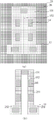
如图1所示,本申请实施例提供一种半导体器件,该半导体器件1包括薄膜晶体管10,所述薄膜晶体管10包括:As shown in FIG. 1, an embodiment of the present application provides a semiconductor device. The
衬底11;
缓冲层13,设置于所述衬底11一侧;a
有源层15,设置于所述缓冲层13远离所述衬底11的一侧;The
其中,所述半导体器件1还包括金属层14,所述金属层14设置于所述有源层15朝向所述缓冲层13的一侧,所述金属层14包括至少一个金属块,且所述金属块与所述有源层15的至少部分直接接触。The
本申请实施例提供一种半导体器件,该半导体器件通过在有源层朝向缓冲层的一侧设置金属层,金属层包括至少一个金属块,使金属块与有源层的至少部分直接接触,则在将有源层由非晶硅转化为多晶硅时,由于金属块的催化作用,使得多晶硅中的晶粒的尺寸交大,减少了多晶硅中的晶界,提高了半导体器件的迁移率。An embodiment of the present application provides a semiconductor device. In the semiconductor device, a metal layer is provided on the side of the active layer facing the buffer layer, and the metal layer includes at least one metal block, so that the metal block is in direct contact with at least part of the active layer, then When the active layer is converted from amorphous silicon to polycrystalline silicon, due to the catalytic effect of the metal block, the size of the crystal grains in the polycrystalline silicon becomes larger, which reduces the grain boundary in the polycrystalline silicon and improves the mobility of the semiconductor device.
需要说明的是,在本申请中的附图中,由于晶界能在微观上看到,因此,本申请中的附图以实线示出晶界的位置以及示意的形状。It should be noted that, in the drawings of the present application, since the grain boundaries can be seen microscopically, the drawings of the present application show the positions and schematic shapes of the grain boundaries with solid lines.
在一种实施例中,所述金属块设置于所述缓冲层与所述有源层之间。通过将金属块设置在缓冲层与有源层之间,使得在形成多晶硅时,金属块能够对非晶硅的反应过程进行催化,金属块作为晶核,使得形成的晶粒的宽度变大,从而减少晶界的数量,提高半导体器件的迁移率。In one embodiment, the metal block is disposed between the buffer layer and the active layer. By arranging the metal block between the buffer layer and the active layer, when forming polysilicon, the metal block can catalyze the reaction process of amorphous silicon, and the metal block acts as a crystal nucleus, so that the width of the formed crystal grain becomes larger, Thereby, the number of grain boundaries is reduced and the mobility of the semiconductor device is improved.
针对金属块设置于缓冲层与有源层之间会导致有源层的厚度变小,影响有源层的电性的问题。在一种实施例中,所述缓冲层在与所述有源层接触的区域设置凹槽,所述金属块设置于所述凹槽内。通过在缓冲层上设置凹槽,使金属块设置在凹槽内,则有源层与缓冲层和金属块接触的表面保持平整,使有源层的电性较好,且金属块作为催化剂使得有源层的晶粒的宽度变大,减小晶界的数量,提高半导体器件的迁移率。Aiming at the problem that the arrangement of the metal block between the buffer layer and the active layer will reduce the thickness of the active layer and affect the electrical properties of the active layer. In one embodiment, a groove is provided in a region of the buffer layer in contact with the active layer, and the metal block is disposed in the groove. By setting grooves on the buffer layer and setting the metal block in the groove, the surface of the active layer in contact with the buffer layer and the metal block remains flat, so that the electrical properties of the active layer are better, and the metal block acts as a catalyst to make The width of the grains of the active layer becomes larger, the number of grain boundaries is reduced, and the mobility of the semiconductor device is improved.
具体的,缓冲层的材料包括氮化硅、氧化硅或者氮化硅和氧化硅的叠层。Specifically, the material of the buffer layer includes silicon nitride, silicon oxide, or a stack of silicon nitride and silicon oxide.
具体的,缓冲层的厚度范围为0.3微米至1微米。Specifically, the thickness of the buffer layer ranges from 0.3 μm to 1 μm.
具体的,凹槽的深度范围为0.05微米至0.5微米,凹槽的宽度范围为0.5微米至2微米,相邻凹槽的相邻边缘的间距为0.5微米至3微米,相邻凹槽的中点的间距为1微米至5微米。通过使凹槽的深度范围为0.05至0.5微米,避免凹槽的深度过大导致缓冲层形成有凹槽的部分厚度较小,使缓冲层阻隔水氧的能力较好;而凹槽的宽度范围为0.5微米至2微米,使得金属块能够设置在凹槽内,对有源层进行催化,减少晶界;使相邻凹槽的相邻边缘的间距为0.5微米至3微米,相邻凹槽的中点的间距为1微米至5微米,则可以使得金属块具有一定的周期,晶粒能够较大,减少晶界。Specifically, the depth of the grooves ranges from 0.05 microns to 0.5 microns, the widths of the grooves range from 0.5 microns to 2 microns, and the spacing between adjacent edges of adjacent grooves is 0.5 microns to 3 microns. The pitch of the dots is 1 micron to 5 microns. By making the depth of the grooves in the range of 0.05 to 0.5 microns, it is avoided that the depth of the grooves is too large and the thickness of the buffer layer where the grooves are formed is smaller, so that the buffer layer has a better ability to block water and oxygen; and the width of the grooves ranges. It is 0.5 microns to 2 microns, so that the metal blocks can be arranged in the grooves, catalyze the active layer, and reduce the grain boundaries; the spacing between the adjacent edges of adjacent grooves is 0.5 microns to 3 microns, and the adjacent grooves The spacing between the midpoints is 1 micron to 5 microns, which can make the metal block have a certain period, the grain can be larger, and the grain boundary can be reduced.
在一种实施例中,所述金属层的材料的熔点小于1410摄氏度。通过采用熔点小于1410摄氏度的材料作为金属层的材料,使得金属层的熔点低于硅的熔点,金属层容易与硅形成固溶体,从而在非晶硅转换为多晶硅的过程中,通过金属层对反应过程进行催化,提高多晶硅的晶粒的尺寸,减少晶界。In one embodiment, the melting point of the material of the metal layer is less than 1410 degrees Celsius. By using a material with a melting point of less than 1410 degrees Celsius as the material of the metal layer, the melting point of the metal layer is lower than the melting point of silicon, and the metal layer is easy to form a solid solution with silicon, so that in the process of converting amorphous silicon to polysilicon, the metal layer reacts The process is catalyzed, increasing the grain size of polysilicon and reducing grain boundaries.
在一种实施例中,金属层的材料包括铝、镍、镓、铟中的一种。通过采用铝、镍、镓、铟作为金属层的材料,使金属层容易与硅形成固溶体,从而在非晶硅转换为多晶硅的过程中,通过金属层对反应过程进行催化,提高多晶硅的晶粒的尺寸,减少晶界。In one embodiment, the material of the metal layer includes one of aluminum, nickel, gallium, and indium. By using aluminum, nickel, gallium, and indium as the material of the metal layer, the metal layer can easily form a solid solution with silicon, so that in the process of converting amorphous silicon to polysilicon, the metal layer catalyzes the reaction process and improves the crystal grain of polysilicon. size, reducing grain boundaries.
针对多晶硅的晶界较多会导致半导体器件的迁移率较低的问题。在一种实施例中,所述半导体器件包括多个薄膜晶体管,至少一个所述薄膜晶体管的有源层无晶界。通过使薄膜晶体管的有源层无晶界,则在粒子的迁移过程中不会受到晶界的阻挡,提高了半导体器件的迁移率。For polysilicon, there are many grain boundaries, which leads to the problem that the mobility of the semiconductor device is low. In one embodiment, the semiconductor device includes a plurality of thin film transistors, and the active layer of at least one of the thin film transistors has no grain boundary. By making the active layer of the thin film transistor free of grain boundaries, the particles will not be blocked by the grain boundaries during the migration process, and the mobility of the semiconductor device is improved.
具体的,如图2所示,所述金属层14包括一个金属块,所述有源层15包括单晶硅,所述单晶硅的直径小于5微米。在有源层的宽度小于5微米时,可以通过在有源层下方设置一个金属块,使得在这个金属块的催化下,非晶硅转化为单晶硅,则仅存在一个晶粒,使得有源层内无晶界,提高半导体器件的迁移率。Specifically, as shown in FIG. 2 , the
在一种实施例中,如图1、图3所示,所述薄膜晶体管10的有源层15包括第一晶粒151,所述第一晶粒151与所述金属块141对应设置,所述第一晶粒151的数量与所述金属块141的数量相等。通过使第一晶粒与金属块对应设置,第一晶粒的数量与金属块的数量相等,则第一晶粒是在金属块的催化下形成,第一晶粒的直径较大,减少晶界的数量,提高半导体器件的迁移率。In an embodiment, as shown in FIG. 1 and FIG. 3 , the
具体的,在通过激光退火的工艺将非晶硅转换为多晶硅时,通过金属块的催化形成第一晶粒,即使由于工艺限制导致第一晶粒之间仍然存有小于第一晶粒的直径的晶粒,但由于第一晶粒的直径较大,仍然可以减少有源层的晶界的数量,提高半导体器件的迁移率。Specifically, when the amorphous silicon is converted into polysilicon through the laser annealing process, the first crystal grains are formed through the catalysis of the metal block, even if there is still a diameter smaller than the first crystal grains between the first crystal grains due to process limitations However, due to the larger diameter of the first crystal grains, the number of grain boundaries of the active layer can still be reduced, and the mobility of the semiconductor device can be improved.
在一种实施例中,所述第一晶粒为圆形或者类圆形,所述第一晶粒的直径为1微米至5微米。通过使第一晶粒的直径为1微米至5微米,使得第一晶粒较大,晶界的数量较少,提高半导体器件的迁移率。In one embodiment, the first crystal grains are circular or quasi-circular, and the diameter of the first crystal grains is 1 to 5 microns. By setting the diameter of the first crystal grains to be 1 micrometer to 5 micrometers, the first crystal grains are made larger and the number of grain boundaries is less, thereby improving the mobility of the semiconductor device.
具体的,如图1、图3所示,所述金属层14包括阵列设置的金属块141,所述有源层15包括多个第一晶粒151,所述金属块141的数量与所述第一晶粒151的数量相等,所述第一晶粒的晶界152位于相邻两个金属块141之间。通过使金属块的数量与第一晶粒的数量相等,使得每个第一晶粒都是通过金属块的催化形成,各个第一晶粒的宽度较大,从而可以减少晶界的数量,提高半导体器件的迁移率,且第一晶粒会沿金属块所处位置向四周生长,从而使第一晶粒的晶界位于相邻两个金属块之间,通过金属块的间距的调整,可以对第一晶粒的宽度进行调整,使晶界数量减少,提高半导体器件的迁移率。Specifically, as shown in FIGS. 1 and 3 , the
具体的,金属层的厚度范围为0.05微米至0.5微米,通过使金属层的厚度为0.05微米至0.5微米,避免金属层的厚度过大导致缓冲层的厚度较小,出现水氧从缓冲层厚度较小的位置入侵。Specifically, the thickness of the metal layer is in the range of 0.05 μm to 0.5 μm. By setting the thickness of the metal layer to be 0.05 μm to 0.5 μm, it is avoided that the thickness of the buffer layer is too large and the thickness of the buffer layer is too small. Smaller location invasion.
具体的,金属块之间的间距为1微米至5微米,通过使金属块的阵列周期为1微米至5微米,使得晶粒的宽度为1微米至5微米,增加晶粒的宽度,减少晶界的数量,提高半导体器件的迁移率。Specifically, the spacing between the metal blocks is 1 μm to 5 μm. By setting the array period of the metal blocks to be 1 μm to 5 μm, the width of the crystal grains is 1 μm to 5 μm. The number of bounds increases the mobility of semiconductor devices.
具体的,金属块的宽度范围为0.5微米至2微米,在设置金属块时,金属块的宽度过小会导致晶粒的宽度较小,从而导致晶界的数量较多,半导体器件的迁移率较低,而使得金属块的宽度过大时,会导致显示面板的开口率较低,影响显示面板的透过率,且金属块的宽度较大时,金属块上可能会存在多个形核位点,导致一个金属块会形成多个晶粒,使得晶粒的宽度较小,晶界较多,因此,设置金属块的宽度为0.5微米至2微米,并控制相邻金属阵列的周期为1微米至5微米,制备晶粒宽度为1微米至5微米的晶粒,使得形成的晶粒的宽度较大,晶界数量较少,提高半导体器件的迁移率。Specifically, the width of the metal block is in the range of 0.5 μm to 2 μm. When setting the metal block, if the width of the metal block is too small, the width of the crystal grain will be smaller, which will lead to a large number of grain boundaries and the mobility of the semiconductor device. If the width of the metal block is too large, the aperture ratio of the display panel will be low, which will affect the transmittance of the display panel. When the width of the metal block is large, there may be multiple nuclei on the metal block. site, resulting in the formation of multiple grains in one metal block, so that the width of the grains is smaller and the grain boundaries are more. Therefore, the width of the metal block is set to be 0.5 μm to 2 μm, and the period of adjacent metal arrays is controlled to be 1 to 5 microns, and to prepare crystal grains with a crystal grain width of 1 to 5 microns, so that the width of the formed crystal grains is larger, the number of grain boundaries is less, and the mobility of the semiconductor device is improved.
在一种实施例中,如图3所示,所述有源层15包括沟道部251和位于所述沟道部251两侧的第一掺杂部252和第二掺杂部253,所述第一掺杂部252及所述第二掺杂部253沿着所述沟道部251之间的连线的形状与所述薄膜晶体管的第一掺杂部252和第二掺杂部253对应的金属块141沿所述沟道部的连线的形状相同。通过使第一掺杂部及第二掺杂部沿着沟道部之间的连线的形状与薄膜晶体管的第一掺杂部和第二掺杂部对应的金属块沿着沟道部的连线的形状相同,使得对于不同设置方式的有源层,可以通过金属阵列的设置方式的改变,使得位于沟道部、第一掺杂部和第二掺杂部的有源层的晶粒的宽度较大,从而可以减少晶界的数量,提高半导体器件的迁移率。In an embodiment, as shown in FIG. 3 , the
具体的,相较于采用非晶硅作为催化剂来增加晶粒尺寸,由于本申请中可以使金属块阵列排布,根据需求的有源层的形状来设置金属块的间距、宽度,从而可以使得有源层的晶粒的宽度较大,晶界数量较少,在有源层的宽度较小时,还可以形成单晶硅,提高半导体器件的迁移率。Specifically, compared to using amorphous silicon as a catalyst to increase the grain size, since the metal blocks can be arranged in an array in the present application, the spacing and width of the metal blocks can be set according to the shape of the active layer required, so that the The width of the crystal grains of the active layer is large, and the number of grain boundaries is small. When the width of the active layer is small, single crystal silicon can also be formed to improve the mobility of the semiconductor device.
在一种实施例中,如图3所示,所述第一掺杂部252和所述第二掺杂部253沿着所述沟道部251之间的连线的形状为直线,所述金属块141沿着所述直线阵列设置。通过使金属块沿直线阵列设置,则位于金属块所处区域的晶粒能够沿着金属块的方向生长,使得晶粒的宽度较大,晶界的数量较少,提高半导体器件的迁移率。In an embodiment, as shown in FIG. 3 , the shape of the
具体的,如图3中的(a)所示,在形成有源层时,对非晶硅层进行处理得到多晶硅层25,具体可以采用激光退火的方式对非晶硅层进行处理,由于有源层15的区域设置有金属块141,使得有源层15的晶粒在金属块141的催化下生长较快,晶粒的宽度较大,而位于有源层15外的区域由于无金属块,使得无效部分26的晶粒的宽度较小,晶界的数量较多;然后对多晶硅层进行刻蚀,如图3中的(b)所示,去除无效部分26并形成有源层的图案,得到有源层15,此时有第一掺杂部及第二掺杂部沿着沟道部之间的连线的形状与第一掺杂部和第二掺杂部对应的金属块沿着沟道部的连线的形状相同,沟道部、第一掺杂部和第二掺杂部沿着金属块的设置方向设置,得到“一字型沟道”的有源层,且该有源层的晶粒的宽度较大,晶界的数量较少,半导体器件的迁移率较高。Specifically, as shown in (a) in FIG. 3, when forming the active layer, the amorphous silicon layer is processed to obtain the
在一种实施例中,如图4所示,所述第一掺杂部252与所述第二掺杂部253位于同一水平线上,所述第一掺杂部252及所述第二掺杂部253沿着所述沟道部251之间的连线的形状为折线,所述金属块141沿着所述折线阵列设置。通过使金属块包括沿着折线阵列设置,使得形成的沟道部、第一掺杂部和第二掺杂部能够形成金属块所形成的形状,且由于金属块的催化作用,沟道部、第一掺杂部和第二掺杂部的晶粒的宽度较大,晶界数量较少,从而提高了半导体器件的迁移率。In one embodiment, as shown in FIG. 4 , the first doped
在一种实施例中,如图4所示,所述沟道部251包括设置于所述第一掺杂部252的垂线方向的第一部分、设置于所述第二掺杂部253的垂线方向的第二部分和与所述第一部分和所述第二部分垂直连接的第三部分,所述第一掺杂部252及所述第二掺杂部253沿着所述沟道部251之间的连线沿着所述第一部分、所述第三部分和所述第二部分设置,所述金属块141沿着所述第一部分、所述第三部分和所述第二部分阵列设置。通过使金属块包括沿着水平线的方向设置的部分、与水平设置的部分垂直的部分以及连接的部分,使得形成的沟道部、第一掺杂部和第二掺杂部能够形成金属块所形成的形状,且由于金属块的催化作用,沟道部、第一掺杂部和第二掺杂部的晶粒的宽度较大,晶界数量较少,从而提高了半导体器件的迁移率。In an embodiment, as shown in FIG. 4 , the
具体的,如图4中的(a)所示,在形成有源层时,对非晶硅层进行处理得到多晶硅层25,具体可以采用激光退火的方式对非晶硅层进行处理,由于有源层15的区域设置有金属块141,使得有源层15的晶粒在金属块141的催化下生长较快,晶粒的宽度较大,而位于有源层15外的区域由于无金属块,使得无效部分26的晶粒的宽度较小,晶界的数量较多;然后对多晶硅层进行刻蚀,如图4中的(b)所示,去除无效部分26并形成有源层的图案,得到有源层15,此时有源层的沟道部、第一掺杂部和第二掺杂部的沿着金属块的设置方向设置,得到“几字型沟道”的有源层,且该有源层的晶粒的宽度较大,晶界的数量较少,半导体器件的迁移率较高。Specifically, as shown in (a) of FIG. 4, when the active layer is formed, the amorphous silicon layer is processed to obtain the
在一种实施例中,如图5所示,所述沟道部251包括连接所述第一掺杂部252和所述第二掺杂部253的第四部分和第五部分,所述第四部分和所述第五部分垂直设置,所述金属块141沿所述第四部分和所述第五部分的方向阵列设置。通过使金属块包括相互垂直的部分,使得在形成有源层时,有源层能够沿着金属块形成,且由于金属块的催化作用,沟道部、第一掺杂部和第二掺杂部的晶粒的宽度较大,晶界数量较少,从而提高了半导体器件的迁移率。In one embodiment, as shown in FIG. 5 , the
具体的,如图5中的(a)所示,在形成有源层时,对非晶硅层进行处理得到多晶硅层25,具体可以采用激光退火的方式对非晶硅层进行处理,由于有源层15的区域设置有金属块141,使得有源层15的晶粒在金属块141的催化下生长较快,晶粒的宽度较大,而位于有源层15外的区域由于无金属块,使得无效部分26的晶粒的宽度较小,晶界的数量较多;然后对多晶硅层进行刻蚀,如图5中的(b)所示,去除无效部分26并形成有源层的图案,得到有源层15,此时有源层的沟道部、第一掺杂部和第二掺杂部的沿着金属块的设置方向设置,得到“L字型沟道”的有源层,且该有源层的晶粒的宽度较大,晶界的数量较少,半导体器件的迁移率较高。Specifically, as shown in (a) of FIG. 5, when the active layer is formed, the amorphous silicon layer is processed to obtain the
需要说明的是,在图3、图4和图5中使位于有源层外的多晶硅下不设置金属块,有源层外的多晶硅的晶粒的宽度较小且晶界的数量较多,但本申请实施例不限于此,例如可以使有源层外的多晶硅下也设置有金属块。It should be noted that in FIG. 3 , FIG. 4 and FIG. 5 , no metal block is provided under the polysilicon outside the active layer, and the grain width of the polysilicon outside the active layer is relatively small and the number of grain boundaries is large. However, the embodiment of the present application is not limited thereto, for example, a metal block may also be disposed under the polysilicon outside the active layer.
在一种实施例中,如图1所示,所述第一晶粒的直径L1与相邻所述金属块的中心点之间的间距L2相等。通过使金属块的中心点之间的间距与第一晶粒的直径相等,从而可以通过金属块的间距和宽度对有源层中的晶粒的宽度进行调整,使有源层中的晶界的数量较少,提高半导体器件的迁移率。In an embodiment, as shown in FIG. 1 , the diameter L1 of the first crystal grain is equal to the distance L2 between the center points of the adjacent metal blocks. By making the spacing between the center points of the metal blocks equal to the diameter of the first crystal grains, the width of the crystal grains in the active layer can be adjusted by the spacing and width of the metal blocks, so that the grain boundaries in the active layer can be adjusted. The number is small, improving the mobility of semiconductor devices.
具体的,金属块等间距设置,在第一晶粒的截面为梯形时,第一晶粒的直径是指梯形的中线处的宽度。Specifically, the metal blocks are arranged at equal intervals, and when the cross section of the first crystal grain is a trapezoid, the diameter of the first crystal grain refers to the width at the center line of the trapezoid.
具体的,上述实施例以金属块等间距设置为例进行了详细描述,但本申请实施例不限于此,例如在沟道部和掺杂部需要的晶粒宽度不同时,可以使金属块的间距不等,且金属块的尺寸不等,则可以使得沟道部和掺杂部的晶粒宽度不同。Specifically, the above-mentioned embodiments have been described in detail by taking metal blocks at equal intervals as an example, but the embodiments of the present application are not limited thereto. If the pitches are not equal and the sizes of the metal blocks are not equal, the crystal grain widths of the channel part and the doping part may be different.
具体的,相较于当前半导体器件中通过在缓冲层内设置非晶硅,然后沉积非晶硅以提高晶粒宽度的方式,当前半导体器件中在缓冲层内设置非晶硅会导致非晶硅的厚度增加,且在激光退火时位于缓冲层内的非晶硅会增加形核位点,容易导致晶粒数量增加,晶粒尺寸增加效果不明显;而本申请实施例采用金属块作为催化剂,由于金属块与非晶硅的材料不同,不会与非晶硅结合导致非晶硅的厚度增大性能改变,且金属块与非晶硅材料不同,不会增加形核位点,能够增大晶粒的宽度,减少晶界的数量,提高半导体器件的迁移率。且相较于采用非晶硅提高晶粒宽度,本申请中采用金属块可以阵列设置,根据有源层的形状设定金属块的间距、宽度,减少有源层内的晶界数量,在有源层的宽度较小时,还可以得到单晶硅,提高半导体器件的迁移率。Specifically, compared with the current semiconductor device in which amorphous silicon is disposed in the buffer layer and then deposited amorphous silicon to increase the grain width, disposing amorphous silicon in the buffer layer in the current semiconductor device will result in amorphous silicon The thickness of the crystal increases, and the amorphous silicon located in the buffer layer will increase the nucleation sites during laser annealing, which will easily lead to an increase in the number of crystal grains, and the effect of increasing the crystal grain size is not obvious. Since the material of the metal block is different from that of amorphous silicon, it will not combine with amorphous silicon to increase the thickness of amorphous silicon, and the performance will change. The width of the grains reduces the number of grain boundaries and improves the mobility of semiconductor devices. And compared with using amorphous silicon to increase the grain width, the metal blocks can be arranged in an array in this application, and the spacing and width of the metal blocks are set according to the shape of the active layer, so as to reduce the number of grain boundaries in the active layer. When the width of the source layer is small, single crystal silicon can also be obtained, and the mobility of the semiconductor device can be improved.
在一种实施例中,如图1所示,半导体器件1还包括遮光层12,遮光层12对应有源层15设置。In an embodiment, as shown in FIG. 1 , the
在一种实施例中,如图1所示,所述半导体器件1还包括栅极绝缘层16、栅极层17、层间绝缘层18、源漏极层19、平坦化层20、第一电极层21、钝化层22和第二电极层23,栅极绝缘层16设置于有源层15远离缓冲层13的一侧,栅极层17设置于栅极绝缘层16远离有源层15的一侧,层间绝缘层18设置于栅极层17远离栅极绝缘层16的一侧,源漏极层19设置于层间绝缘层18远离栅极层17的一侧,平坦化层20设置于源漏极层19远离层间绝缘层18的一侧,第一电极层21设置于平坦化层20远离源漏极层19的一侧,钝化层22设置于第一电极层21远离平坦化层20的一侧,第二电极层23设置于钝化层22远离第一电极层21的一侧。In an embodiment, as shown in FIG. 1 , the
同时,本申请实施例提供一种半导体器件的制备方法,该半导体器件的制备方法包括:Meanwhile, an embodiment of the present application provides a method for preparing a semiconductor device, and the method for preparing a semiconductor device includes:
提供衬底,并在衬底上形成遮光层,在遮光层上沉积缓冲层,并通过曝光显影刻蚀工艺形成凹槽;该步骤对应的半导体器件的结构如图6中的(a)所示;Provide a substrate, and form a light-shielding layer on the substrate, deposit a buffer layer on the light-shielding layer, and form a groove through an exposure, development and etching process; the structure of the semiconductor device corresponding to this step is shown in (a) in Figure 6 ;
然后在缓冲层上沉积金属层;该步骤对应的半导体器件的结构如图6中的(b)所示;Then a metal layer is deposited on the buffer layer; the structure of the semiconductor device corresponding to this step is shown in (b) in FIG. 6 ;
具体的,如图6中的(b)所示,在缓冲层上沉积金属薄膜24时,由于缓冲层上设有凹槽,金属24会在形成有凹槽的位置形成金属块。Specifically, as shown in (b) of FIG. 6 , when the metal
然后在金属层上形成光阻;该步骤对应的半导体器件的结构如图6中的(c)所示;Then a photoresist is formed on the metal layer; the structure of the semiconductor device corresponding to this step is shown in (c) in FIG. 6 ;
具体的,如图6中的(c)所示,通过设置光阻35,使半导体器件能够流平,便于后续制程。Specifically, as shown in (c) of FIG. 6 , by arranging the
然后通过干蚀刻将光阻和位于缓冲层上的金属薄膜进行整面刻蚀,并控制刻蚀过程使凹槽外的金属刻蚀完毕后结束刻蚀,保留凹槽内的金属;该步骤对应的半导体器件的结构如图6中的(d)所示;Then, the photoresist and the metal film on the buffer layer are etched on the entire surface by dry etching, and the etching process is controlled so that the etching is completed after the metal outside the groove is etched, and the metal in the groove is retained; this step corresponds to The structure of the semiconductor device is shown in (d) in Figure 6;
然后在缓冲层上沉积非晶硅层;该步骤对应的半导体器件的结构如图7中的(a)所示;Then, an amorphous silicon layer is deposited on the buffer layer; the structure of the semiconductor device corresponding to this step is shown in (a) in FIG. 7 ;
具体的,如图7中的(a)所示,通过在缓冲层上形成非晶硅层41,使得可以通过非晶硅层形成多晶硅。Specifically, as shown in (a) of FIG. 7 , by forming the
然后对非晶硅层进行激光退火处理,使得非晶硅层转变为多晶硅层;该步骤对应的半导体器件的结构如图7中的(b)所示;Then, laser annealing is performed on the amorphous silicon layer, so that the amorphous silicon layer is transformed into a polysilicon layer; the structure of the semiconductor device corresponding to this step is shown in (b) in FIG. 7 ;
具体的,如图7中的(b)所示,在由非晶硅层转变为多晶硅层25时,对于存在金属块的区域和不存在金属块的区域,多晶硅的晶粒的宽度不同,多晶硅的晶界的数量不同,且存在金属块的区域的多晶硅的晶粒的宽度较大,晶界数量较少,使得形成有源层时,有源层的晶粒的宽度较大,晶界数量较少,提高半导体器件的迁移率。Specifically, as shown in (b) of FIG. 7 , when the amorphous silicon layer is transformed into the
具体的,该步骤以非晶硅层转变为多晶硅层为例进行说明,但本申请实施例不限于此,例如可以由非晶硅层转变为单晶硅。Specifically, this step is described by taking the transformation of the amorphous silicon layer into the polycrystalline silicon layer as an example, but the embodiment of the present application is not limited to this, for example, the amorphous silicon layer can be transformed into single crystal silicon.
然后对多晶硅层进行曝光显影和刻蚀,形成有源层;该步骤对应的半导体器件的结构如图7中的(c)所示;Then, the polysilicon layer is exposed, developed and etched to form an active layer; the structure of the semiconductor device corresponding to this step is shown in (c) in FIG. 7 ;
然后在有源层上形成栅极绝缘层、栅极层、层间绝缘层、源漏极层、平坦化层、第一电极层、钝化层和第二电极层,得到半导体器件。Then, a gate insulating layer, a gate electrode layer, an interlayer insulating layer, a source and drain layer, a planarization layer, a first electrode layer, a passivation layer and a second electrode layer are formed on the active layer to obtain a semiconductor device.
同时,本申请实施例提供一种电子装置,该电子装置包括如上述实施例任一所述的半导体器件。Meanwhile, an embodiment of the present application provides an electronic device, and the electronic device includes the semiconductor device described in any one of the above embodiments.
具体的,电子装置可以为液晶显示面板、也可以为有机发光二极管显示面板。Specifically, the electronic device may be a liquid crystal display panel or an organic light emitting diode display panel.
根据上述实施例可知:According to above-mentioned embodiment can know:
本申请实施例提供一种半导体器件和电子装置;该半导体器件包括薄膜晶体管,薄膜晶体管包括衬底、缓冲层和有源层,缓冲层设置于衬底一侧,有源层设置于缓冲层远离衬底的一侧,其中,半导体器件还包括金属层,金属层设置于有源层朝向缓冲层的一侧,金属层包括至少一个金属块,且金属块与有源层的至少部分直接接触。本申请通过在有源层朝向缓冲层的一侧设置金属层,金属层包括至少一个金属块,使金属块与有源层的至少部分直接接触,则在将有源层由非晶硅转化为多晶硅时,由于金属块的催化作用,使得多晶硅中的晶粒的尺寸交大,减少了多晶硅中的晶界,提高了半导体器件的迁移率。Embodiments of the present application provide a semiconductor device and an electronic device; the semiconductor device includes a thin film transistor, and the thin film transistor includes a substrate, a buffer layer and an active layer, the buffer layer is disposed on one side of the substrate, and the active layer is disposed far from the buffer layer. One side of the substrate, wherein the semiconductor device further includes a metal layer, the metal layer is disposed on the side of the active layer facing the buffer layer, the metal layer includes at least one metal block, and the metal block is in direct contact with at least part of the active layer. In the present application, by disposing a metal layer on the side of the active layer facing the buffer layer, the metal layer includes at least one metal block, so that the metal block is in direct contact with at least part of the active layer, the active layer is converted from amorphous silicon to In the case of polysilicon, due to the catalytic effect of the metal block, the size of the crystal grains in the polysilicon becomes larger, which reduces the grain boundaries in the polysilicon and improves the mobility of the semiconductor device.
在上述实施例中,对各个实施例的描述都各有侧重,某个实施例中没有详述的部分,可以参见其他实施例的相关描述。In the above-mentioned embodiments, the description of each embodiment has its own emphasis. For parts that are not described in detail in a certain embodiment, reference may be made to the relevant descriptions of other embodiments.
以上对本申请实施例所提供的一种半导体器件和电子装置进行了详细介绍,本文中应用了具体个例对本申请的原理及实施方式进行了阐述,以上实施例的说明只是用于帮助理解本申请的技术方案及其核心思想;本领域的普通技术人员应当理解:其依然可以对前述各实施例所记载的技术方案进行修改,或者对其中部分技术特征进行等同替换;而这些修改或者替换,并不使相应技术方案的本质脱离本申请各实施例的技术方案的范围。The semiconductor device and electronic device provided by the embodiments of the present application have been described in detail above. The principles and implementations of the present application are described in this article by using specific examples. The descriptions of the above embodiments are only used to help understand the present application. Those of ordinary skill in the art should understand that: they can still modify the technical solutions recorded in the foregoing embodiments, or perform equivalent replacements to some of the technical features; and these modifications or replacements, and The essence of the corresponding technical solutions is not deviated from the scope of the technical solutions of the embodiments of the present application.
Claims (15)
Priority Applications (3)
| Application Number | Priority Date | Filing Date | Title |
|---|---|---|---|
| CN202210804923.7A CN115241278B (en) | 2022-07-08 | 2022-07-08 | Semiconductor devices and electronic devices |
| US17/759,866 US12148839B2 (en) | 2022-07-08 | 2022-07-28 | Semiconductor device and electronic device |
| PCT/CN2022/108652 WO2024007385A1 (en) | 2022-07-08 | 2022-07-28 | Semiconductor device and electronic apparatus |
Applications Claiming Priority (1)
| Application Number | Priority Date | Filing Date | Title |
|---|---|---|---|
| CN202210804923.7A CN115241278B (en) | 2022-07-08 | 2022-07-08 | Semiconductor devices and electronic devices |
Publications (2)
| Publication Number | Publication Date |
|---|---|
| CN115241278A true CN115241278A (en) | 2022-10-25 |
| CN115241278B CN115241278B (en) | 2025-10-21 |
Family
ID=83671415
Family Applications (1)
| Application Number | Title | Priority Date | Filing Date |
|---|---|---|---|
| CN202210804923.7A Active CN115241278B (en) | 2022-07-08 | 2022-07-08 | Semiconductor devices and electronic devices |
Country Status (3)
| Country | Link |
|---|---|
| US (1) | US12148839B2 (en) |
| CN (1) | CN115241278B (en) |
| WO (1) | WO2024007385A1 (en) |
Citations (7)
| Publication number | Priority date | Publication date | Assignee | Title |
|---|---|---|---|---|
| KR20020035909A (en) * | 2000-11-07 | 2002-05-16 | 한민구 | Manufacturing Process of Polycrystalline Silicon Thin Film Transistor |
| US20060163733A1 (en) * | 2005-01-25 | 2006-07-27 | Au Optronics Corp. | Semiconductor structure having multilayer of polysilicon and display panel applied with the same |
| US20080102550A1 (en) * | 2003-11-27 | 2008-05-01 | Samsung Sdi Co., Ltd. | Thin film transistor using a metal induced crystallization process and method for fabricating the same and active matrix flat panel display using the thin film transistor |
| US20130273724A1 (en) * | 2012-04-12 | 2013-10-17 | Seung Ki Joo | Method for crystallizing amorphous silicon thin film and method for fabricating poly crystalline thin film transistor using the same |
| US20150155390A1 (en) * | 2013-03-11 | 2015-06-04 | Ordos Yuansheng Optoelectronics Co., Ltd. | Manufacturing method of polysilicon layer, and polysilicon thin film transistor and manufacturing method thereof |
| CN109817644A (en) * | 2019-01-30 | 2019-05-28 | 武汉华星光电半导体显示技术有限公司 | A kind of tft array substrate and preparation method thereof |
| CN109841668A (en) * | 2017-12-22 | 2019-06-04 | 恩智浦美国有限公司 | Semiconductor device and its manufacturing method with doped region |
Family Cites Families (9)
| Publication number | Priority date | Publication date | Assignee | Title |
|---|---|---|---|---|
| TW317643B (en) * | 1996-02-23 | 1997-10-11 | Handotai Energy Kenkyusho Kk | |
| US7745822B2 (en) * | 2003-06-27 | 2010-06-29 | Nec Corporation | Thin film transistor and thin film transistor substrate including a polycrystalline semiconductor thin film having a large heat capacity part and a small heat capacity part |
| US8222116B2 (en) * | 2006-03-03 | 2012-07-17 | Semiconductor Energy Laboratory Co., Ltd. | Method for manufacturing semiconductor device |
| WO2009000136A1 (en) * | 2007-06-22 | 2008-12-31 | The Hong Kong University Of Science And Technology | Polycrystalline silicon thin film transistors with bridged-grain structures |
| TWI653755B (en) * | 2013-09-12 | 2019-03-11 | 日商新力股份有限公司 | Display device, manufacturing method thereof, and electronic device |
| CN104576753B (en) | 2014-12-29 | 2018-06-26 | 昆山国显光电有限公司 | A kind of low-temperature polysilicon film transistor and its manufacturing method |
| CN106206622B (en) | 2016-09-23 | 2019-05-10 | 京东方科技集团股份有限公司 | Array substrate and preparation method thereof, and display device |
| CN106601823A (en) | 2016-12-29 | 2017-04-26 | 京东方科技集团股份有限公司 | Thin film transistor and manufacturing method thereof |
| CN112071868B (en) * | 2020-09-18 | 2024-09-13 | 京东方科技集团股份有限公司 | LTPS TFT array substrate and display device |
-
2022
- 2022-07-08 CN CN202210804923.7A patent/CN115241278B/en active Active
- 2022-07-28 US US17/759,866 patent/US12148839B2/en active Active
- 2022-07-28 WO PCT/CN2022/108652 patent/WO2024007385A1/en not_active Ceased
Patent Citations (7)
| Publication number | Priority date | Publication date | Assignee | Title |
|---|---|---|---|---|
| KR20020035909A (en) * | 2000-11-07 | 2002-05-16 | 한민구 | Manufacturing Process of Polycrystalline Silicon Thin Film Transistor |
| US20080102550A1 (en) * | 2003-11-27 | 2008-05-01 | Samsung Sdi Co., Ltd. | Thin film transistor using a metal induced crystallization process and method for fabricating the same and active matrix flat panel display using the thin film transistor |
| US20060163733A1 (en) * | 2005-01-25 | 2006-07-27 | Au Optronics Corp. | Semiconductor structure having multilayer of polysilicon and display panel applied with the same |
| US20130273724A1 (en) * | 2012-04-12 | 2013-10-17 | Seung Ki Joo | Method for crystallizing amorphous silicon thin film and method for fabricating poly crystalline thin film transistor using the same |
| US20150155390A1 (en) * | 2013-03-11 | 2015-06-04 | Ordos Yuansheng Optoelectronics Co., Ltd. | Manufacturing method of polysilicon layer, and polysilicon thin film transistor and manufacturing method thereof |
| CN109841668A (en) * | 2017-12-22 | 2019-06-04 | 恩智浦美国有限公司 | Semiconductor device and its manufacturing method with doped region |
| CN109817644A (en) * | 2019-01-30 | 2019-05-28 | 武汉华星光电半导体显示技术有限公司 | A kind of tft array substrate and preparation method thereof |
Also Published As
| Publication number | Publication date |
|---|---|
| US12148839B2 (en) | 2024-11-19 |
| WO2024007385A1 (en) | 2024-01-11 |
| US20240186420A1 (en) | 2024-06-06 |
| CN115241278B (en) | 2025-10-21 |
Similar Documents
| Publication | Publication Date | Title |
|---|---|---|
| CN100544030C (en) | Channel-etch thin film transistor | |
| CN1309034C (en) | Method of fabricating bottom-gated polycrystalline silicon thin film transistor | |
| CN102842601B (en) | Array substrate and manufacture method thereof | |
| TW202324540A (en) | Semiconductor device and manufacturing method thereof | |
| CN115188829B (en) | Semiconductor devices and electronic devices | |
| CN105914134B (en) | Electronic device, thin film transistor (TFT) and array base palte and preparation method thereof | |
| CN112928125B (en) | Array substrate and display panel | |
| CN106298646B (en) | The production method of TFT substrate | |
| CN111710725A (en) | Double gate electrode metal oxide thin film transistor and preparation method thereof | |
| WO2024036762A1 (en) | Thin film transistor of vertical structure and electronic device | |
| US12148768B2 (en) | Array substrate and display panel | |
| CN1901158A (en) | Method of manufacturing thin film transistor substrate | |
| US7678619B2 (en) | Method of manufacturing a thin film transistor matrix substrate | |
| CN115241278A (en) | Semiconductor device and electronic apparatus | |
| CN101261962B (en) | Active element array substrate and manufacturing method thereof | |
| WO2022205509A1 (en) | Array substrate | |
| CN107910338B (en) | Array substrate and display device | |
| JPH08330593A (en) | Method for manufacturing thin film transistor | |
| CN114545695A (en) | Display panel, preparation method thereof and display terminal | |
| CN105140238A (en) | Array substrate and fabrication method thereof | |
| CN217983347U (en) | Array substrate and display panel | |
| CN115000087A (en) | Array substrate and preparation method thereof | |
| CN1815321A (en) | Method for manufacturing lower substrate for liquid crystal display device | |
| CN114373771A (en) | Array substrate, manufacturing method and display device | |
| WO2019085011A1 (en) | Method for fabricating low-temperature polycrystalline silicon thin film and transistor |
Legal Events
| Date | Code | Title | Description |
|---|---|---|---|
| PB01 | Publication | ||
| PB01 | Publication | ||
| SE01 | Entry into force of request for substantive examination | ||
| SE01 | Entry into force of request for substantive examination | ||
| GR01 | Patent grant | ||
| GR01 | Patent grant |