Disclosure of Invention
Technical problem to be solved
Based on the above problems, the present disclosure provides a room temperature isostatic pressing metal bonding method for a wafer, so as to alleviate the technical problems of high cost, low efficiency, device damage caused by uneven high temperature or pressure in wafer bonding in the prior art.
(II) technical scheme
In the present disclosure, a room temperature isostatic pressing metal bonding method of a wafer is provided, including:
step S1: cleaning a wafer to be bonded, and removing impurities on the surface of the wafer;
step S2: depositing a metal intermediate layer on the surface of the cleaned wafer;
step S3: aligning and attaching the front surfaces of two wafers respectively subjected to metal intermediate layer deposition, fixing the two wafers, then placing the wafers into a mold, and vacuumizing and sealing the mold by using a vacuum pump;
step S4: placing the well-sealed die in a high-pressure cylinder of an isostatic pressing bonding machine, locking the high-pressure cylinder, and filling a liquid pressure medium into the high-pressure cylinder to ensure that the die is completely immersed in the liquid pressure medium and is directly contacted with the liquid pressure medium;
step S5: and setting bonding pressure and bonding time, bonding the wafer to be bonded, releasing pressure after bonding is finished, and taking out the bonded wafer to complete room-temperature isostatic pressing metal bonding of the wafer.
In an embodiment of the present disclosure, the preparation material of the wafer includes: si, GaAs, InP, GaN, SiC, AlN, or Ga2O3Any one of the base structure materials.
In the embodiment of the present disclosure, in step S1, a chemical cleaning method is adopted.
In an embodiment of the present disclosure, in step S2, the deposition method of the metal intermediate layer includes: at least one of sputtering, chemical vapor deposition, evaporation, electroplating, or laser metal deposition.
In an embodiment of the present disclosure, in step S2, the metal intermediate layer includes:
the adhesion layer metal is prepared from the following materials: at least one of Ti, Ni or Cr; and
bonding the intermediate layer, preparing a material comprising: at least one of Au, Cu, Ag, In, Ti, Sn, Pt, Cr, Ge or Ni.
In the embodiment of the disclosure, the thickness of the adhesion layer metal is 5-100 nm.
In the embodiment of the disclosure, the thickness of the bonding intermediate layer is 100-500 nm.
In the embodiment of the present disclosure, in step S5, the bonding process of the wafer is performed under room temperature conditions.
In the embodiment of the disclosure, in step S5, the bonding pressure is 30-200MPa, and the bonding time is 30-120 min.
In an embodiment of the present disclosure, the effective bonding area fraction of the wafer is greater than 95%.
(III) advantageous effects
According to the technical scheme, the room-temperature isostatic pressing metal bonding method for the wafer has at least one or part of the following beneficial effects:
(1) the thickness of the metal intermediate layer is reduced by one magnitude, which is beneficial to reducing the interface thermal resistance;
(2) the wafer bonding of the ultrathin metal intermediate layer can be realized at room temperature, and the influence of high temperature on the performance of materials and devices is avoided;
(3) the requirement on the surface state of the wafer is not high, the surface of the material does not need to be subjected to additional polishing and modification treatment, the process is simplified, the cost is greatly reduced, and the bonding efficiency is improved;
(4) the sample is uniformly stressed, physical damage to the wafer is avoided, and the performance of the material and the device is not influenced;
(5) the method is not limited by the size and shape of a sample, and can meet the requirement of multi-size wafer bonding.
Detailed Description
The invention provides a room temperature isostatic pressing metal bonding method of a wafer, which still belongs to the category of metal bonding and can be used in the fields of integrated circuit manufacturing, Micro Electro Mechanical System (MEMS) packaging, multifunctional chip integration and the like, but the method is essentially different from metal eutectic bonding, so that the thickness of a metal intermediate layer is reduced by one magnitude, the wafer bonding of an ultrathin metal intermediate layer can be realized at room temperature, and the influence of high temperature on the performance of materials and devices is avoided; the requirement on the surface state of the wafer is not high, and the surface does not need to be subjected to additional polishing and activation treatment; in the bonding process, the high-pressure cylinder applies higher pressure to the wafer from all directions equally through the liquid pressure medium, so that the physical damage to the wafer is avoided, and the performance of materials and devices is not affected.
For the purpose of promoting a better understanding of the objects, aspects and advantages of the present disclosure, reference is made to the following detailed description taken in conjunction with the accompanying drawings.
In an embodiment of the present disclosure, a room temperature isostatic pressing metal bonding method for a wafer is provided, which is shown in fig. 1 to 4, and includes:
step S1: cleaning a wafer to be bonded, and removing impurities on the surface of the wafer;
step S2: depositing a metal intermediate layer on the surface of the cleaned wafer;
step S3: aligning and attaching the front surfaces of two wafers respectively subjected to metal intermediate layer deposition, fixing the two wafers, then placing the wafers into a mold, and vacuumizing and sealing the mold by using a vacuum pump;
step S4: placing the well-sealed die in a high-pressure cylinder of an isostatic pressing bonding machine, locking the high-pressure cylinder, and filling a liquid pressure medium into the high-pressure cylinder to ensure that the die is completely immersed in the liquid pressure medium and is directly contacted with the liquid pressure medium;
step S5: and setting bonding pressure and bonding time, bonding the wafer to be bonded, releasing pressure after bonding is finished, and taking out the bonded wafer to complete room-temperature isostatic pressing metal bonding of the wafer.
In the step S1, the wafer to be bonded is cleaned by first ultrasonically cleaning the wafer to be bonded with acetone, ethanol and deionized water for 10-60min, then rinsing with deionized water, and then adding HCl: H2Ultrasonically cleaning a wafer to be bonded by a solution with the ratio of O to O being 1: 1-10 for 5-30min, washing by deionized water, and finally drying by a nitrogen gun;
in the step S2, depositing a metal intermediate layer on the cleaned wafer surface, where the metal intermediate layer is a Ti/Au double metal layer, the metal Ti is used as an adhesion layer, the thickness of the metal Ti is 5-50nm, the sputtering power is 100-; the metal of the adhesion layer is one of Ti, Ni or Cr, the bonding intermediate layer is one of Au, Cu or Al, and the preparation method is one of magnetron sputtering, electron beam evaporation or electroplating; preferentially, performing direct current sputtering and radio frequency sputtering of Ti and Au metal targets on the wafer respectively by adopting a magnetron sputtering device;
in the step S3, aligning and bonding the front surfaces of the two wafers on which the metal intermediate layer is deposited, fixing the two wafers, then placing the wafers into a mold, vacuumizing the mold by using a vacuum pump, and sealing the mold after exhausting air in the mold;
in the step S4, as shown in fig. 2, the high pressure cylinder 7 is fixed on the supporting frame 12 by the screw 8, and is provided with the lifting system 6; placing a well-sealed die in a high-pressure cylinder of an isostatic pressing bonding machine, closing an upper cover 1, a lower cover 9, locking a high-pressure cylinder 7, arranging a sealing ring 2 in the high-pressure cylinder, filling a liquid pressure medium 3 through a pressure medium pipeline 10, placing the die in a sample basket 4, completely immersing the die in the liquid pressure medium 3, directly contacting the liquid pressure medium, applying a certain pressure to the pressure medium in the cylinder by using high-pressure equipment, and uniformly applying the pressure to a wafer to be bonded through the pressure medium in an all-directional way manner; when the isostatic pressing bonding machine works, a sample 5 sealed in a die is placed into a high-pressure cylinder, a high-pressure oil pump is used for flushing a liquid pressure medium into the high-pressure cylinder along a pressure medium pipeline 10 and is in direct contact with the die, so that isotropic pressure can be applied to the sample, and a pressure gauge 11 is used for monitoring a real-time pressure state;
and in the step S5, entering an isostatic pressing bonding machine control system, setting bonding pressure and bonding time, bonding the wafer to be bonded, releasing pressure and taking out the bonded wafer after bonding is finished, wherein the bonding pressure is 30-200MPa, and the bonding time is 30-120 min.
As shown in fig. 3, the bonded ultrasonic scanning microscope shows that the effective bonding area of the wafer can reach 96.37%, and the unbonded rate is 3.63%.
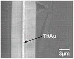
Fig. 4 is a cross-sectional sem image of a bonded wafer according to the present disclosure, showing a clear bonding interface and a uniform thickness of the metal intermediate layer.
So far, the embodiments of the present disclosure have been described in detail with reference to the accompanying drawings. It is to be noted that, in the attached drawings or in the description, the implementation modes not shown or described are all the modes known by the ordinary skilled person in the field of technology, and are not described in detail. Further, the above definitions of the various elements and methods are not limited to the various specific structures, shapes or arrangements of parts mentioned in the examples, which may be easily modified or substituted by those of ordinary skill in the art.
From the above description, those skilled in the art should clearly understand the room temperature isostatic metal bonding method for the wafer of the present disclosure.
In conclusion, the present disclosure provides a room temperature isostatic pressing metal bonding method for a wafer, which adopts an isostatic pressing technique to ensure that a sample is uniformly stressed, so as to avoid physical damage, reduce the thickness of a metal intermediate layer to the maximum extent, and contribute to reducing interface thermal resistance; the requirements on the surface state of the wafer are lowered, additional polishing and modification treatment on the surface of the material are not needed, the cost is greatly reduced, and the bonding efficiency is improved; the method is not limited by the size and shape of a sample, and can meet the requirement of multi-size wafer bonding.
It should also be noted that directional terms, such as "upper", "lower", "front", "rear", "left", "right", and the like, used in the embodiments are only directions referring to the drawings, and are not intended to limit the scope of the present disclosure. Throughout the drawings, like elements are represented by like or similar reference numerals. Conventional structures or constructions will be omitted when they may obscure the understanding of the present disclosure.
And the shapes and sizes of the respective components in the drawings do not reflect actual sizes and proportions, but merely illustrate the contents of the embodiments of the present disclosure. Furthermore, in the claims, any reference signs placed between parentheses shall not be construed as limiting the claim.
Unless otherwise indicated, the numerical parameters set forth in the specification and attached claims are approximations that can vary depending upon the desired properties sought to be obtained by the present disclosure. In particular, all numbers expressing quantities of ingredients, reaction conditions, and so forth used in the specification and claims are to be understood as being modified in all instances by the term "about". Generally, the expression is meant to encompass variations of ± 10% in some embodiments, 5% in some embodiments, 1% in some embodiments, 0.5% in some embodiments by the specified amount.
Furthermore, the word "comprising" does not exclude the presence of elements or steps not listed in a claim. The word "a" or "an" preceding an element does not exclude the presence of a plurality of such elements.
The use of ordinal numbers such as "first," "second," "third," etc., in the specification and claims to modify a corresponding element does not by itself connote any ordinal number of the element or any ordering of one element from another or the order of manufacture, and the use of the ordinal numbers is only used to distinguish one element having a certain name from another element having a same name.
In addition, unless steps are specifically described or must occur in sequence, the order of the steps is not limited to that listed above and may be changed or rearranged as desired by the desired design. The embodiments described above may be mixed and matched with each other or with other embodiments based on design and reliability considerations, i.e., technical features in different embodiments may be freely combined to form further embodiments.
Those skilled in the art will appreciate that the modules in the device in an embodiment may be adaptively changed and disposed in one or more devices different from the embodiment. The modules or units or components of the embodiments may be combined into one module or unit or component, and furthermore they may be divided into a plurality of sub-modules or sub-units or sub-components. All of the features disclosed in this specification (including any accompanying claims, abstract and drawings), and all of the processes or elements of any method or apparatus so disclosed, may be combined in any combination, except combinations where at least some of such features and/or processes or elements are mutually exclusive. Each feature disclosed in this specification (including any accompanying claims, abstract and drawings) may be replaced by alternative features serving the same, equivalent or similar purpose, unless expressly stated otherwise. Also in the unit claims enumerating several means, several of these means may be embodied by one and the same item of hardware.
Similarly, it should be appreciated that in the foregoing description of exemplary embodiments of the disclosure, various features of the disclosure are sometimes grouped together in a single embodiment, figure, or description thereof for the purpose of streamlining the disclosure and aiding in the understanding of one or more of the various disclosed aspects. However, the disclosed method should not be interpreted as reflecting an intention that: that is, the claimed disclosure requires more features than are expressly recited in each claim. Rather, as the following claims reflect, disclosed aspects lie in less than all features of a single foregoing disclosed embodiment. Thus, the claims following the detailed description are hereby expressly incorporated into this detailed description, with each claim standing on its own as a separate embodiment of this disclosure.
The above-mentioned embodiments are intended to illustrate the objects, aspects and advantages of the present disclosure in further detail, and it should be understood that the above-mentioned embodiments are only illustrative of the present disclosure and are not intended to limit the present disclosure, and any modifications, equivalents, improvements and the like made within the spirit and principle of the present disclosure should be included in the scope of the present disclosure.