CN110731003A - Molybdenum-containing low resistivity films - Google Patents
Molybdenum-containing low resistivity films Download PDFInfo
- Publication number
- CN110731003A CN110731003A CN201880038116.0A CN201880038116A CN110731003A CN 110731003 A CN110731003 A CN 110731003A CN 201880038116 A CN201880038116 A CN 201880038116A CN 110731003 A CN110731003 A CN 110731003A
- Authority
- CN
- China
- Prior art keywords
- layer
- molybdenum
- reducing agent
- substrate
- tungsten
- Prior art date
- Legal status (The legal status is an assumption and is not a legal conclusion. Google has not performed a legal analysis and makes no representation as to the accuracy of the status listed.)
- Granted
Links
Images


Classifications
-
- H10P14/43—
-
- H10W20/0526—
-
- C—CHEMISTRY; METALLURGY
- C23—COATING METALLIC MATERIAL; COATING MATERIAL WITH METALLIC MATERIAL; CHEMICAL SURFACE TREATMENT; DIFFUSION TREATMENT OF METALLIC MATERIAL; COATING BY VACUUM EVAPORATION, BY SPUTTERING, BY ION IMPLANTATION OR BY CHEMICAL VAPOUR DEPOSITION, IN GENERAL; INHIBITING CORROSION OF METALLIC MATERIAL OR INCRUSTATION IN GENERAL
- C23C—COATING METALLIC MATERIAL; COATING MATERIAL WITH METALLIC MATERIAL; SURFACE TREATMENT OF METALLIC MATERIAL BY DIFFUSION INTO THE SURFACE, BY CHEMICAL CONVERSION OR SUBSTITUTION; COATING BY VACUUM EVAPORATION, BY SPUTTERING, BY ION IMPLANTATION OR BY CHEMICAL VAPOUR DEPOSITION, IN GENERAL
- C23C16/00—Chemical coating by decomposition of gaseous compounds, without leaving reaction products of surface material in the coating, i.e. chemical vapour deposition [CVD] processes
- C23C16/06—Chemical coating by decomposition of gaseous compounds, without leaving reaction products of surface material in the coating, i.e. chemical vapour deposition [CVD] processes characterised by the deposition of metallic material
-
- C—CHEMISTRY; METALLURGY
- C23—COATING METALLIC MATERIAL; COATING MATERIAL WITH METALLIC MATERIAL; CHEMICAL SURFACE TREATMENT; DIFFUSION TREATMENT OF METALLIC MATERIAL; COATING BY VACUUM EVAPORATION, BY SPUTTERING, BY ION IMPLANTATION OR BY CHEMICAL VAPOUR DEPOSITION, IN GENERAL; INHIBITING CORROSION OF METALLIC MATERIAL OR INCRUSTATION IN GENERAL
- C23C—COATING METALLIC MATERIAL; COATING MATERIAL WITH METALLIC MATERIAL; SURFACE TREATMENT OF METALLIC MATERIAL BY DIFFUSION INTO THE SURFACE, BY CHEMICAL CONVERSION OR SUBSTITUTION; COATING BY VACUUM EVAPORATION, BY SPUTTERING, BY ION IMPLANTATION OR BY CHEMICAL VAPOUR DEPOSITION, IN GENERAL
- C23C18/00—Chemical coating by decomposition of either liquid compounds or solutions of the coating forming compounds, without leaving reaction products of surface material in the coating; Contact plating
- C23C18/02—Chemical coating by decomposition of either liquid compounds or solutions of the coating forming compounds, without leaving reaction products of surface material in the coating; Contact plating by thermal decomposition
- C23C18/08—Chemical coating by decomposition of either liquid compounds or solutions of the coating forming compounds, without leaving reaction products of surface material in the coating; Contact plating by thermal decomposition characterised by the deposition of metallic material
-
- H—ELECTRICITY
- H10—SEMICONDUCTOR DEVICES; ELECTRIC SOLID-STATE DEVICES NOT OTHERWISE PROVIDED FOR
- H10B—ELECTRONIC MEMORY DEVICES
- H10B12/00—Dynamic random access memory [DRAM] devices
- H10B12/01—Manufacture or treatment
- H10B12/02—Manufacture or treatment for one transistor one-capacitor [1T-1C] memory cells
-
- H—ELECTRICITY
- H10—SEMICONDUCTOR DEVICES; ELECTRIC SOLID-STATE DEVICES NOT OTHERWISE PROVIDED FOR
- H10B—ELECTRONIC MEMORY DEVICES
- H10B12/00—Dynamic random access memory [DRAM] devices
- H10B12/30—DRAM devices comprising one-transistor - one-capacitor [1T-1C] memory cells
- H10B12/48—Data lines or contacts therefor
- H10B12/488—Word lines
-
- H10P14/418—
-
- H10P14/432—
-
- H10P95/00—
-
- H10P95/90—
-
- H10W20/033—
-
- H10W20/045—
-
- H10W20/056—
-
- H10W20/057—
-
- H10W20/42—
-
- H—ELECTRICITY
- H10—SEMICONDUCTOR DEVICES; ELECTRIC SOLID-STATE DEVICES NOT OTHERWISE PROVIDED FOR
- H10B—ELECTRONIC MEMORY DEVICES
- H10B41/00—Electrically erasable-and-programmable ROM [EEPROM] devices comprising floating gates
- H10B41/20—Electrically erasable-and-programmable ROM [EEPROM] devices comprising floating gates characterised by three-dimensional arrangements, e.g. with cells on different height levels
- H10B41/23—Electrically erasable-and-programmable ROM [EEPROM] devices comprising floating gates characterised by three-dimensional arrangements, e.g. with cells on different height levels with source and drain on different levels, e.g. with sloping channels
- H10B41/27—Electrically erasable-and-programmable ROM [EEPROM] devices comprising floating gates characterised by three-dimensional arrangements, e.g. with cells on different height levels with source and drain on different levels, e.g. with sloping channels the channels comprising vertical portions, e.g. U-shaped channels
-
- H—ELECTRICITY
- H10—SEMICONDUCTOR DEVICES; ELECTRIC SOLID-STATE DEVICES NOT OTHERWISE PROVIDED FOR
- H10B—ELECTRONIC MEMORY DEVICES
- H10B43/00—EEPROM devices comprising charge-trapping gate insulators
- H10B43/20—EEPROM devices comprising charge-trapping gate insulators characterised by three-dimensional arrangements, e.g. with cells on different height levels
- H10B43/23—EEPROM devices comprising charge-trapping gate insulators characterised by three-dimensional arrangements, e.g. with cells on different height levels with source and drain on different levels, e.g. with sloping channels
- H10B43/27—EEPROM devices comprising charge-trapping gate insulators characterised by three-dimensional arrangements, e.g. with cells on different height levels with source and drain on different levels, e.g. with sloping channels the channels comprising vertical portions, e.g. U-shaped channels
-
- H10W20/425—
Landscapes
- Chemical & Material Sciences (AREA)
- Engineering & Computer Science (AREA)
- Physics & Mathematics (AREA)
- Manufacturing & Machinery (AREA)
- Condensed Matter Physics & Semiconductors (AREA)
- Power Engineering (AREA)
- Microelectronics & Electronic Packaging (AREA)
- Computer Hardware Design (AREA)
- General Physics & Mathematics (AREA)
- General Chemical & Material Sciences (AREA)
- Chemical Kinetics & Catalysis (AREA)
- Organic Chemistry (AREA)
- Metallurgy (AREA)
- Mechanical Engineering (AREA)
- Materials Engineering (AREA)
- Thermal Sciences (AREA)
- Chemical Vapour Deposition (AREA)
- Electrodes Of Semiconductors (AREA)
- Crystallography & Structural Chemistry (AREA)
- Internal Circuitry In Semiconductor Integrated Circuit Devices (AREA)
- Semiconductor Memories (AREA)
Abstract
本文提供了用于逻辑和存储器应用的低电阻金属化堆叠结构以及相关的制造方法。在一些实现方案中,所述方法涉及:在衬底上提供含钨(W)层;并且在所述含W层上沉积含钼(Mo)层。在一些实现方式中,该方法涉及直接在介电或氮化钛(TiN)衬底上沉积含Mo层,而没有中间的含W层。
Low-resistance metallization stacks for logic and memory applications and related fabrication methods are provided herein. In some implementations, the methods involve: providing a tungsten (W)-containing layer on a substrate; and depositing a molybdenum (Mo)-containing layer on the W-containing layer. In some implementations, the methods involve depositing the Mo-containing layer directly on a dielectric or titanium nitride (TiN) substrate without an intervening W-containing layer.
Description
相关申请的交叉引用CROSS-REFERENCE TO RELATED APPLICATIONS
本申请根据35U.S.C.§119要求于2017年4月10日提交的美国临时专利申请No.62/483,857的利益,其内容以引用方式并入本文。This application claims the benefit of US Provisional Patent Application No. 62/483,857, filed April 10, 2017, under 35 U.S.C. § 119, the contents of which are incorporated herein by reference.
背景技术Background technique
这里提供的背景描述是为了一般地呈现本公开的背景的目的。在该背景技术部分以及在提交时不会以其他方式认为是现有技术的描述的方面中描述的程度上,目前署名的发明人的工作既不明确地也不隐含地被承认为针对本公开的现有技术。The background description provided herein is for the purpose of generally presenting the context of the disclosure. To the extent described in this Background section and aspects that would not otherwise be considered prior art at the time of filing, the work of the presently named inventors is neither expressly nor implicitly acknowledged as a Published prior art.
使用化学气相沉积(CVD)技术的钨(W)膜沉积是半导体制造工艺的不可或缺的部分。例如,钨膜可用作水平互连形式中的低电阻电连接件,相邻金属层之间的通孔,以及第一金属层和硅衬底上的设备之间的触点。钨膜也可用在多种存储器应用中,包括用于动态随机存取存储器(DRAM)的掩埋字线(bWL)架构的形成中,以及逻辑应用中。在bWL沉积的示例中,钨层可被沉积在氮化钛(TiN)阻隔层上以使用WF6通过CVD过程形成TiN/W双层。然而,特征尺寸和膜厚度的持续减小给TiN/W膜堆叠件带来了各种挑战。这些挑战包括较薄的膜的较高的电阻率和破坏TiN势垒性能。Tungsten (W) film deposition using chemical vapor deposition (CVD) techniques is an integral part of the semiconductor manufacturing process. For example, tungsten films can be used as low resistance electrical connections in the form of horizontal interconnects, vias between adjacent metal layers, and contacts between a first metal layer and a device on a silicon substrate. Tungsten films are also used in a variety of memory applications, including the formation of buried word line (bWL) architectures for dynamic random access memory (DRAM), and in logic applications. In the example of bWL deposition, a tungsten layer may be deposited on a titanium nitride (TiN) barrier layer to form a TiN/W bilayer by a CVD process using WF 6 . However, the continued reduction in feature size and film thickness presents various challenges for TiN/W film stacks. These challenges include higher resistivity of thinner films and disrupted TiN barrier properties.
发明内容SUMMARY OF THE INVENTION
本公开的一个方面涉及包括以下步骤的方法:在衬底上提供含钨(W)层;并且在所述含W层上沉积含钼(Mo)层。在一些实施方案中,所述含W层是WCN层。在一些实施方案中,所述含W层是W成核层。在一些实施方案中,所述含W层是由一种或多种氯化钨前体沉积的。在一些实施方案中,所述含Mo层是杂质小于1(原子)%的Mo层。在一些实施方案中,所述方法还包括对所述含Mo层进行热退火。在一些实施方案中,通过将所述含W层暴露于还原剂和含Mo前体来沉积所述含Mo层,并且所述含Mo前体选自:六氟化钼(MoF6)、五氯化钼(MoCl5)、二氯二氧化钼(MoO2Cl2)、四氯氧化钼(MoOCl4)和六羰基钼(Mo(CO)6)。在一些实施方案中,在暴露于所述含Mo前体期间的衬底温度小于550℃。在一些实施方案中,所述衬底在第一衬底温度下暴露于所述还原剂,并且在第二衬底温度下暴露于所述含Mo前体,其中所述第一衬底温度小于所述第二衬底温度。在一些实施方案中,所述还原剂是含硼还原剂和含硅还原剂的混合物。One aspect of the present disclosure relates to a method comprising the steps of: providing a tungsten (W)-containing layer on a substrate; and depositing a molybdenum (Mo)-containing layer on the W-containing layer. In some embodiments, the W-containing layer is a WCN layer. In some embodiments, the W-containing layer is a W nucleation layer. In some embodiments, the W-containing layer is deposited from one or more tungsten chloride precursors. In some embodiments, the Mo-containing layer is a Mo layer with an impurity of less than 1 atomic %. In some embodiments, the method further includes thermally annealing the Mo-containing layer. In some embodiments, the Mo-containing layer is deposited by exposing the W-containing layer to a reducing agent and a Mo-containing precursor selected from the group consisting of: molybdenum hexafluoride (MoF 6 ), five Molybdenum chloride (MoCl 5 ), molybdenum dioxide dichloride (MoO 2 Cl 2 ), molybdenum oxytetrachloride (MoOCl 4 ) and molybdenum hexacarbonyl (Mo(CO) 6 ). In some embodiments, the substrate temperature during exposure to the Mo-containing precursor is less than 550°C. In some implementations, the substrate is exposed to the reducing agent at a first substrate temperature and to the Mo-containing precursor at a second substrate temperature, wherein the first substrate temperature is less than the second substrate temperature. In some embodiments, the reducing agent is a mixture of a boron-containing reducing agent and a silicon-containing reducing agent.
本公开的另一个方面涉及包括以下步骤的方法:在第一衬底温度下使还原剂气体流入容纳衬底的处理室,以在所述衬底上形成保形还原剂层;以及在第二衬底温度下将所述保形还原剂层暴露于含钼(Mo)前体以将所述还原剂层转化为钼。在一些实施方案中,所述第一衬底温度小于所述第二衬底温度。在一些实施方案中,所述还原剂是含硼还原剂和含硅还原剂的混合物。在一些实施方案中,所述第一衬底温度不超过400℃,并且所述第二衬底温度至少为500℃。在一些实施方案中,所述方法进一步包括使所述钼退火。Another aspect of the present disclosure relates to a method comprising the steps of: flowing a reductant gas into a processing chamber containing a substrate at a first substrate temperature to form a conformal reductant layer on the substrate; and at a second substrate temperature The conformal reductant layer is exposed to a molybdenum (Mo)-containing precursor at a substrate temperature to convert the reductant layer to molybdenum. In some implementations, the first substrate temperature is less than the second substrate temperature. In some embodiments, the reducing agent is a mixture of a boron-containing reducing agent and a silicon-containing reducing agent. In some embodiments, the first substrate temperature does not exceed 400°C, and the second substrate temperature is at least 500°C. In some embodiments, the method further comprises annealing the molybdenum.
本公开的另一个方面涉及包括以下步骤的方法:脉冲式发送(pulsing)还原剂,其中所述还原剂是含硼(B)的、含硅(Si)的或含钼(Mo)的;并且脉冲式发送含Mo前体,其中所述含Mo前体通过所述还原剂或其产物还原以在所述衬底上形成含有B、Si和Ge中的一种或更多种的多组分含钨膜。在一些实施方案中,所述多组分含钨膜包含介于5%和60%(原子)之间的B、Si或Ge。在一些实施方案中,所述介于5%和60%(原子)之间的B、Si或Ge由所述还原剂提供。Another aspect of the present disclosure relates to a method comprising the steps of: pulsing a reducing agent, wherein the reducing agent is boron (B)-containing, silicon (Si)-containing, or molybdenum (Mo)-containing; and pulsing a Mo-containing precursor, wherein the Mo-containing precursor is reduced by the reducing agent or product thereof to form a multicomponent containing one or more of B, Si, and Ge on the substrate Tungsten containing film. In some embodiments, the multi-component tungsten-containing film comprises between 5 and 60 atomic % of B, Si, or Ge. In some embodiments, the between 5 and 60 atomic % of the B, Si or Ge is provided by the reducing agent.
本公开的另一方面是用于执行本文公开的方法的装置。关于附图进一步讨论了这些和其他特征。Another aspect of the present disclosure is an apparatus for performing the methods disclosed herein. These and other features are discussed further with respect to the figures.
附图说明Description of drawings
图1A和1B是根据各种实施方案的包括钼(Mo)的材料堆叠件的示意性示例。1A and 1B are schematic examples of stacks of materials including molybdenum (Mo) according to various embodiments.
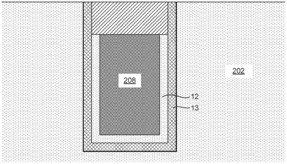
图2描绘了包括Mo埋字线(bWL)的DRAM架构的示意性示例。FIG. 2 depicts a schematic example of a DRAM architecture including Mo buried word lines (bWLs).
图3A描绘了3D NAND结构中的Mo字线的示意性示例。Figure 3A depicts a schematic example of a Mo word line in a 3D NAND structure.
图3B描绘了在包括Mo字线和保形阻挡层的Mo填充之后部分制造的3D NAND结构的3D特征的2D渲染。3B depicts a 2D rendering of a 3D feature of a partially fabricated 3D NAND structure after Mo filling including Mo wordlines and conformal barrier layers.
图4A和4B提供了根据所公开的实施方案执行的方法的工艺流程图。4A and 4B provide process flow diagrams of methods performed in accordance with the disclosed embodiments.
图5和6是对于用于在钨(W)成核层上CVD沉积Mo的不同的衬底温度和室压强下,分别显示Mo厚度(埃)与CVD持续时间(秒)的函数关系和Mo电阻率(μΩ-cm)与Mo厚度(埃)的函数关系的图。Figures 5 and 6 are graphs showing Mo thickness (Angstroms) as a function of CVD duration (sec) and Mo resistance, respectively, for different substrate temperatures and chamber pressures used for CVD deposition of Mo on tungsten (W) nucleation layers Plot of rate (μΩ-cm) as a function of Mo thickness (Angstrom).
图7和8是对于在不同的衬底温度和室压强下在WCN上CVD沉积Mo,分别显示Mo生长速率和电阻率与Mo膜厚度的函数关系的图。Figures 7 and 8 are graphs showing Mo growth rate and resistivity as a function of Mo film thickness, respectively, for CVD deposition of Mo on WCN at different substrate temperatures and chamber pressures.
图9是示出CVD沉积的Mo层的厚度和电阻率与WCN下伏层厚度的函数关系的图。Figure 9 is a graph showing the thickness and resistivity of a CVD deposited Mo layer as a function of WCN underlying layer thickness.
图10是显示在800℃退火后,沉积在2nm WCN上的各种不同的厚度的Mo堆叠件的堆叠件电阻率降低的曲线图。Figure 10 is a graph showing the decrease in stack resistivity for various thicknesses of Mo stacks deposited on 2 nm WCN after annealing at 800°C.
图11是适用于根据本发明描述的实施方案进行沉积工艺的处理系统的框图。11 is a block diagram of a processing system suitable for use in a deposition process according to embodiments described herein.
具体实施方式Detailed ways
在以下的描述中,阐述了许多具体细节以提供对所呈现的实施方案的充分理解。所公开的实施方案可以在没有这些具体细节中的一些或全部的情况下实施。在其他实例中,未详细描述公知的处理操作,以避免不必要地使所公开的实施方案模糊不清。虽然将结合具体实施方案描述所公开的实施方案,但应当理解的是其并不旨在限制所公开的实施方案。In the following description, numerous specific details are set forth in order to provide a thorough understanding of the presented embodiments. The disclosed embodiments may be practiced without some or all of these specific details. In other instances, well-known processing operations have not been described in detail to avoid unnecessarily obscuring the disclosed embodiments. While the disclosed embodiments will be described in conjunction with specific embodiments, it will be understood that they are not intended to limit the disclosed embodiments.
本文提供了用于逻辑和存储器应用的低电阻金属化堆叠结构。图1A和1B是根据各种实施方案的包含钼(Mo)的材料堆叠件的示意性示例。图1A和1B示出了特定堆叠件中的材料的顺序,并且可以与任何适当的架构和应用一起使用,如下面关于图2和3进一步描述的。在图1A的示例中,衬底102在其上沉积有Mo层108。衬底102可以是硅或其他半导体晶片,例如200mm晶片、300mm晶片或450mm晶片,其包括具有沉积在其上的一或多个材料(例如介电材料、导电材料或半导体材料)层的晶片。所述方法还可以应用于在诸如玻璃、塑料等的其他衬底上形成金属化堆叠结构。This article provides low resistance metallization stack structures for logic and memory applications. 1A and 1B are schematic examples of material stacks comprising molybdenum (Mo) according to various embodiments. FIGS. 1A and 1B illustrate the sequence of materials in a particular stack, and may be used with any suitable architecture and application, as described further below with respect to FIGS. 2 and 3 . In the example of FIG. 1A,
在图1A中,介电层104在衬底102上。介电层104可以直接沉积在衬底102的半导体(例如,Si)表面上,或者可以存在任何数量的中间层。介电层的示例包括经掺杂和未经掺杂的氧化硅、氮化硅和氧化铝层,具体示例包括经掺杂或未经掺杂的SiO2层和Al2O3层。另外,在图1A中,扩散阻挡层106设置在Mo层108和介电层104之间。扩散阻挡层的示例包括氮化钛(TiN)、钛/氮化钛(Ti/TiN)、氮化钨(WN)和氮碳化钨(WCN)。扩散阻挡层的其他示例是如下所述的多组分含钼膜。Mo层108是该结构的主要导体。如下面进一步讨论的,Mo层108可以包括Mo成核层和主体Mo层。此外,在一些实施方案中,Mo层108可以沉积在钨(W)或含W的生长初始化层上。In FIG. 1A ,
图1B示出了材料堆叠件的另一示例。在该示例中,堆叠件包括衬底102、介电层104,其中Mo层108沉积在电介质层104上,而没有中间扩散阻挡层。如同在图1A的示例中,Mo层108可以包括Mo成核层和主体Mo层,并且在一些实施方案中,Mo层108可以沉积在钨(W)或含W的生长初始化层上。通过使用比W具有较低的电子平均自由程的Mo作为主要导体,可以得到较低的电阻率的薄膜。Figure IB shows another example of a material stack. In this example, the stack includes a
尽管图1A和1B示出了金属化堆叠件的示例,但是方法和所得堆叠件不受限于此。例如,在一些实施方案中,可以将Mo直接沉积在具有或不具有W初始化层的Si或其他半导体衬底上。Although FIGS. 1A and 1B illustrate examples of metallized stacks, the methods and resulting stacks are not so limited. For example, in some embodiments, Mo can be deposited directly on Si or other semiconductor substrates with or without a W initialization layer.
上面且进一步在下面描述的材料堆叠件可以用于各种实施方案中。图2、3A和3B提供了其中可以使用含Mo的堆叠件的结构的示例。图2描述了包括硅衬底202中的Mo掩埋字线(bWL)208的DRAM架构的示意性示例。所述Mo bWL是在硅衬底202中蚀刻的沟槽中形成的。沟槽的衬里是共形阻挡层206和绝缘层204,绝缘层204被设置在所述共形阻挡层206和硅衬底202之间。在图2的示例中,绝缘层204可以是栅极氧化物层,其由高k介电材料(例如氧化硅或氮化硅材料)形成。在本文所公开的一些实施方案中,所述共形阻挡层是TiN或含钨层。在一些实施方案中,如果TiN用作阻挡层,则在保形阻挡层206和Mo bWL 208之间可以存在保形的含钨生长初始化层。替代地,可以将Mo bWL 208直接沉积在TiN或其他扩散阻挡层上。The material stacks described above and further below may be used in various embodiments. 2, 3A and 3B provide examples of structures in which Mo-containing stacks may be used. FIG. 2 depicts a schematic example of a DRAM architecture including Mo buried word lines (bWL) 208 in a silicon substrate 202 . The Mo bWL is formed in trenches etched in the silicon substrate 202 . The trenches are lined by a conformal barrier layer 206 and an insulating layer 204 disposed between the conformal barrier layer 206 and the silicon substrate 202 . In the example of FIG. 2, insulating layer 204 may be a gate oxide layer formed of a high-k dielectric material such as a silicon oxide or silicon nitride material. In some embodiments disclosed herein, the conformal barrier layer is a TiN or tungsten-containing layer. In some embodiments, a conformal tungsten-containing growth initiation layer may be present between the conformal barrier layer 206 and the Mo bWL 208 if TiN is used as the barrier layer. Alternatively, Mo bWL 208 can be deposited directly on TiN or other diffusion barriers.
图3A描述了3D NAND结构323中的Mo字线308的示意性示例。在图3B中,示出了填充Mo之后部分制造的3D NAND结构的3D特征的2D渲染图,其包括字线308和共形阻挡层306。图3B是具有示于图中的柱收缩部324的填充区域的横截面描绘图,柱收缩部324代表将在顶视图而不是横截面视图中可见的收缩部。所述共形阻挡层306可以是与图2中的共形阻挡层206相关的上文所述的含TiN或钨层。在一些实施方案中,含钨膜可用作阻挡层和用于后续的CVD Mo沉积的成核层,如下文所述。如果将TiN用作阻挡层,则在阻挡层和字线之间可以存在共形的含钨的生长初始化层。替代地,可以将Mo字线308直接沉积在TiN或其他扩散阻挡层上。FIG. 3A depicts a schematic example of a
形成含Mo堆叠件的方法包括气相沉积技术,例如CVD和脉冲成核层(PNL)沉积。在PNL技术中,共反应物、任选的清扫气体和含Mo前体的脉冲被顺序地注入反应室并从反应室清除。该过程以循环方式重复,直到达到所需的厚度。PNL广泛地体现了连续添加用于在半导体衬底上反应的反应物的任何循环过程,其包括原子层沉积(ALD)技术。在本文所述的方法中,PNL可用于沉积Mo成核层和/或基于W的生长起始化层。成核层通常是薄的共形层,其有利于随后在其上沉积主体材料。根据各种实现方式,可以在特征的任何填充之前和/或在填充特征期间的随后的时点沉积成核层。Methods of forming Mo-containing stacks include vapor deposition techniques such as CVD and pulsed nucleation layer (PNL) deposition. In the PNL technique, pulses of co-reactants, optional purge gas, and Mo-containing precursor are sequentially injected into and purged from the reaction chamber. This process is repeated in a circular fashion until the desired thickness is achieved. PNL broadly embodies any cyclic process that continuously adds reactants for reaction on a semiconductor substrate, including atomic layer deposition (ALD) techniques. In the methods described herein, PNL can be used to deposit Mo nucleation layers and/or W-based growth initiation layers. Nucleation layers are typically thin conformal layers that facilitate subsequent deposition of host material thereon. According to various implementations, the nucleation layer may be deposited before any filling of the feature and/or at a later point during filling of the feature.
用于沉积钨成核层的PNL技术在美国专利No.6,635,965;No.7,005,372;No.7,141,494;No.7,589,017,No.7,772,114,No.7,955,972和No.8,058,170中有记载。成核层厚度可取决于成核层沉积方法以及所希望的主体沉积质量。通常,成核层厚度足以支撑高质量、均匀的主体沉积。示例的范围可以从10埃到100埃。PNL techniques for depositing tungsten nucleation layers are described in US Patent Nos. 6,635,965; 7,005,372; 7,141,494; 7,589,017, 7,772,114, 7,955,972 and 8,058,170. The nucleation layer thickness may depend on the nucleation layer deposition method and the desired quality of the bulk deposition. Typically, the nucleation layer is thick enough to support high quality, uniform bulk deposition. Examples may range from 10 angstroms to 100 angstroms.
在许多实现方式中,Mo主体层的沉积可以通过CVD工艺进行,其中还原剂和含Mo前体流入沉积室以在该特征中沉积主体层。可以使用惰性载气来输送一种或多种反应物流,其可以预先混合或者可以不预先混合。与PNL或ALD工艺不同,该操作通常涉及使反应物连续地流动直到期望的量被沉积。在某些实现方式中,CVD操作可以以多个阶段进行,反应物的多个连续和同时流动的多个时段被转向的一个或多个反应物流的时段分开。In many implementations, the deposition of the Mo host layer can be performed by a CVD process in which a reducing agent and a Mo-containing precursor are flowed into a deposition chamber to deposit the host layer in the feature. One or more reactant streams may be delivered using an inert carrier gas, which may or may not be premixed. Unlike PNL or ALD processes, this operation typically involves flowing the reactants continuously until the desired amount is deposited. In certain implementations, a CVD operation may be performed in multiple stages, with multiple periods of continuous and simultaneous flow of reactants separated by periods of diverted one or more reactant streams.
含钼的前体包括六氟化钼(MoF6)、五氯化钼(MoCl5)、二氯二氧化钼(MoO2Cl2)、四氯氧化钼(MoOCl4)和六羰基钼(Mo(CO)6)。可以使用有机金属前体,例如甲硅烷基环戊二烯基钼和甲硅烷基烯丙基钼配合物。含Mo前体可以是卤化物前体,其包括MoF6和MoCl5,以及具有可以形成稳定分子的两个或更多个卤素的混合卤化物前体。混合卤化物前体的一个示例是MoClxBry,其中x和y是大于0的可以形成稳定的分子的任何数字。Molybdenum-containing precursors include molybdenum hexafluoride (MoF 6 ), molybdenum pentachloride (MoCl 5 ), molybdenum dichloride (MoO 2 Cl 2 ), molybdenum oxytetrachloride (MoOCl 4 ), and molybdenum hexacarbonyl (Mo (CO) 6 ). Organometallic precursors such as silylcyclopentadienyl molybdenum and silyl allyl molybdenum complexes can be used. Mo-containing precursors can be halide precursors including MoF6 and MoCl5 , as well as mixed halide precursors with two or more halogens that can form stable molecules. An example of a mixed halide precursor is MoClxBry, where x and y are any numbers greater than 0 that can form stable molecules.
W基生长初始化层上的含Mo层Mo-containing layer on W-based growth initialization layer
在某些实施方案中,提供了包括在钨(W)基生长初始化层上的含钼(Mo)层的结构。还提供了形成含Mo膜的方法。In certain embodiments, structures are provided that include a molybdenum (Mo)-containing layer on a tungsten (W) based growth initiation layer. Methods of forming Mo-containing films are also provided.
W基生长初始化层可以是任何含W的层。在一些实施方案中,它是成核层,即薄的保形层,其用于促进随后在其上形成主体材料。在一些实施方案中,W基生长初始化层是本体含W层,其本身可以沉积在成核层上。当用于特征填充时,可以沉积成核层以保形地涂覆特征的侧壁和底部。符合下伏特征的底部和侧壁对于支持高质量沉积至关重要。根据各种实施方案,可以通过PNL和CVD中的一者或两者来沉积W基生长初始化层。例如,CVD层可以沉积在PNL层上。The W-based growth initialization layer can be any W-containing layer. In some embodiments, it is a nucleation layer, ie, a thin conformal layer that serves to facilitate subsequent formation of the host material thereon. In some embodiments, the W-based growth initiation layer is a bulk W-containing layer, which may itself be deposited on the nucleation layer. When used for feature filling, a nucleation layer can be deposited to conformally coat the sidewalls and bottom of the feature. Bottom and sidewalls that conform to the underlying features are critical to support high-quality deposition. According to various embodiments, the W-based growth initiation layer may be deposited by one or both of PNL and CVD. For example, a CVD layer can be deposited on the PNL layer.
在一些实施方案中,含W层是元素W层。可以通过包括PNL或CVD方法的任何适当方法来沉积这样的层。元素W与二元膜(如WC或WN)和三元膜(如WCN)有所区别,但是它可能包含一些杂质。它可以被称为W层或W膜。In some embodiments, the W-containing layer is an elemental W layer. Such layers may be deposited by any suitable method including PNL or CVD methods. Elemental W is distinguished from binary films (such as WC or WN) and ternary films (such as WCN), but it may contain some impurities. It can be called as W layer or W film.
在一些实施方案中,W基生长层是低电阻率W(LRW)膜。根据某些实施方案的低电阻率钨的沉积在美国专利No.7,772,114中描述。特别是,No.7,772,114专利描述了在将W CVD沉积在PNL W层上之前,先将PNL W成核层暴露于还原剂中。LRW膜具有较大的晶粒尺寸,可为较大的Mo晶粒生长提供良好的模板。In some embodiments, the W-based growth layer is a low resistivity W (LRW) film. Deposition of low resistivity tungsten according to certain embodiments is described in US Patent No. 7,772,114. In particular, Patent No. 7,772,114 describes exposing the PNL W nucleation layer to a reducing agent prior to W CVD deposition on the PNL W layer. The LRW film has a larger grain size, which provides a good template for the growth of larger Mo grains.
在一些实施方案中,W基生长层是使用含硼还原剂(例如,B2H6)或含硅还原剂(例如,SiH4)中的一种或多种作为共反应物沉积的PNL W成核层。例如,可以采用一个或多个S/W循环(其中S/W是指先提供硅烷脉冲,然后提供六氟化钨(WF6)或其他含钨前体脉冲)以沉积PNL W成核层,在PNL W成核层上沉积钼层。在另一示例中,可以采用一个或多个B/W循环(其中B/W是指先提供乙硼烷脉冲,随后提供WF6或其他含钨前体脉冲)以沉积PNL W成核层,在该层上沉积Mo层。B/W和S/W循环均可用于沉积PNL W成核层。使用含硼还原剂和含硅还原剂中的一种或两种的PNL工艺的示例描述于美国专利No.7,262,125;No.7,589,017;No.7,772,114;No.7,955,972;No.8,058,170;No.9,236,297和No.9,583,385。In some embodiments, the W-based growth layer is PNL W deposited using one or more of a boron-containing reducing agent (eg, B 2 H 6 ) or a silicon-containing reducing agent (eg, SiH 4 ) as co-reactants nucleation layer. For example, one or more S/W cycles (where S/W refers to a pulse of silane followed by a pulse of tungsten hexafluoride (WF 6 ) or other tungsten-containing precursor) can be used to deposit a PNL W nucleation layer, where A molybdenum layer is deposited on the PNL W nucleation layer. In another example, one or more cycles of B/W (where B/W refers to a pulse of diborane followed by a pulse of WF or other tungsten - containing precursor) can be employed to deposit a PNL W nucleation layer, at Mo layer is deposited on this layer. Both B/W and S/W cycles can be used to deposit PNL W nucleation layers. Examples of PNL processes using one or both of boron- and silicon-containing reducing agents are described in US Patent Nos. 7,262,125; 7,589,017; 7,772,114; 7,955,972; 8,058,170; No. 9,583,385.
在一些实施方案中,W基生长层是使用氯化钨(WClx)前体(例如六氯化钨(WCl6)或五氯化钨(WCl5))沉积的W层或其他含W层。在美国专利No.9,595,470、美国专利公开No.20150348840和美国专利申请No.15/398,462中描述了使用氯化钨沉积含W层。In some embodiments, the W-based growth layer is a W layer or other W-containing layer deposited using a tungsten chloride (WCl x ) precursor such as tungsten hexachloride (WCl 6 ) or tungsten pentachloride (WCl 5 ) . The use of tungsten chloride to deposit W-containing layers is described in US Patent No. 9,595,470, US Patent Publication No. 20150348840, and US Patent Application No. 15/398,462.
在一些实施方案中,W基生长层是低氟W层。美国专利No.9,613,818描述了沉积低氟W层的顺序CVD方法。美国专利公开No.2016/0351444中描述了沉积低氟W层的PNL方法。In some embodiments, the W-based growth layer is a low-fluorine W layer. US Patent No. 9,613,818 describes a sequential CVD method for depositing a low fluorine W layer. A PNL method for depositing a low-fluorine W layer is described in US Patent Publication No. 2016/0351444.
在一些实施方案中,W基生长层是WN、WC或WCN膜。在美国专利No.7,005,372、No.8,053,365、No.8,278,216和美国专利申请No.15/474,383中的每一种中都描述了沉积WN、WC或WCN中的一种或多种的方法。In some embodiments, the W-based growth layer is a WN, WC, or WCN film. Methods of depositing one or more of WN, WC, or WCN are described in each of US Patent Nos. 7,005,372, 8,053,365, 8,278,216, and US Patent Application No. 15/474,383.
W基生长层不限于以上给出的示例,而可以是通过包括ALD、PNL、CVD或物理气相沉积(PVD)方法的任何适当方法沉积的任何W膜或其他含W膜。ALD、PNL和CVD沉积涉及暴露于含W前体。除WF6和WClx前体外,含W前体的示例还包括六羰基钨(W(CO)6)和有机金属前体,例如MDNOW(甲基环戊二烯基-二羰基亚硝酰基-钨)和EDNOW(乙基环戊二烯基-二羰基亚硝酰基-钨)。在许多ALD、PNL和CVD沉积工艺中,还原剂用于还原含W前体。示例包括氢气(H2)、硅烷(SiH4)、乙硅烷(Si2H6)肼(N2H4)、乙硼烷(B2H6)和锗烷(GeH4)。The W-based growth layer is not limited to the examples given above, but may be any W film or other W-containing film deposited by any suitable method including ALD, PNL, CVD or physical vapor deposition (PVD) methods. ALD, PNL and CVD depositions involve exposure to W-containing precursors. In addition to WF6 and WClx precursors, examples of W-containing precursors include tungsten hexacarbonyl (W(CO) 6 ) and organometallic precursors such as MDNOW (methylcyclopentadienyl-dicarbonylnitrosyl- tungsten) and EDNOW (ethylcyclopentadienyl-dicarbonylnitrosyl-tungsten). In many ALD, PNL and CVD deposition processes, reducing agents are used to reduce W-containing precursors. Examples include hydrogen (H 2 ), silane (SiH 4 ), disilane (Si 2 H 6 ), hydrazine (N 2 H 4 ), diborane (B 2 H 6 ), and germane (GeH 4 ).
也如上所述,本文所述的含W膜可以包括一定量的其他化合物、掺杂剂和/或杂质,例如氮、碳、氧、硼、磷、硫、硅、锗等,具体取决于所使用的特定的前体和工艺。该膜中的钨含量范围可以从20%到100%(原子)的钨。在许多实现方式中,所述膜是富含钨的,具有至少50%(原子)钨,或甚至至少约60%、75%、90%或99%(原子)的钨。在一些实现方式中,膜可以是元素钨(W)和其他含钨化合物(如WC、WN等)的混合物。As also described above, the W-containing films described herein may include certain amounts of other compounds, dopants, and/or impurities, such as nitrogen, carbon, oxygen, boron, phosphorous, sulfur, silicon, germanium, etc., depending on the The specific precursors and processes used. The tungsten content in the film can range from 20% to 100% (atomic) tungsten. In many implementations, the film is tungsten rich, having at least 50 atomic percent tungsten, or even at least about 60, 75, 90, or 99 atomic percent tungsten. In some implementations, the film may be a mixture of elemental tungsten (W) and other tungsten-containing compounds (eg, WC, WN, etc.).
可以通过包括ALD或CVD的任何适当方法将含Mo膜沉积在W基生长初始化层上。在一些实施方案中,可以使用顺序CVD工艺。顺序CVD工艺在美国专利No.9,613,818中有描述,该专利通过引用并入本文。The Mo-containing film can be deposited on the W-based growth initiation layer by any suitable method including ALD or CVD. In some embodiments, a sequential CVD process may be used. A sequential CVD process is described in US Patent No. 9,613,818, which is incorporated herein by reference.
含Mo膜的沉积可涉及同时或顺序地将W基生长初始化层暴露于含Mo前体和还原剂或其他共反应剂。含Mo前体的示例包括MoF6、MoCl5、MoOCl4和Mo(CO)6。可以使用有机金属前体,例如甲硅烷基环戊二烯基钼和甲硅烷基烯丙基钼配合物。可以通过改变前体和共反应物的分压来调节Mo膜的纯度(例如,通过O含量计量)。Deposition of Mo-containing films may involve simultaneous or sequential exposure of the W-based growth initiation layer to Mo-containing precursors and reducing agents or other co-reactants. Examples of Mo-containing precursors include MoF 6 , MoCl 5 , MoOCl 4 , and Mo(CO) 6 . Organometallic precursors such as silylcyclopentadienyl molybdenum and silyl allyl molybdenum complexes can be used. The purity of the Mo film can be adjusted (eg, by O content metering) by varying the partial pressures of the precursors and co-reactants.
Mo沉积过程中的衬底温度可以在300℃至750℃之间,并且在特定实施方案中,可以在450℃至550℃之间。衬底温度将取决于热预算和沉积化学过程。热预算取决于应用,同时高沉积温度对于存储器应用而言可能不是问题,但它可能超过逻辑应用程序的热预算。The substrate temperature during Mo deposition can be between 300°C and 750°C, and in certain embodiments, between 450°C and 550°C. The substrate temperature will depend on the thermal budget and deposition chemistry. The thermal budget is application dependent, while high deposition temperatures may not be an issue for memory applications, but it may exceed the thermal budget for logic applications.
含W生长初始化层的存在使得能在较低的温度下进行沉积。例如,由于Mo-Cl键的强度,不能在低于550℃的温度下沉积来自MoCl5或MoOCl4的Mo。但是,对于含W生长初始化层,可以在低于550℃的温度下进行沉积。在Mo沉积期间的室压强可以为例如5托至60托。The presence of the W-containing growth initiation layer enables deposition at lower temperatures. For example, Mo from MoCl5 or MoOCl4 cannot be deposited at temperatures below 550 °C due to the strength of the Mo - Cl bond. However, for W-containing growth initiation layers, deposition can be performed at temperatures below 550°C. The chamber pressure during Mo deposition can be, for example, 5 to 60 Torr.
在一些实施方案中,H2用作还原剂,而不是用更强的还原剂,例如SiH4或B2H6。当使用含氧的含Mo的前体时,这些更强的还原剂会导致不良的富氧界面。含Mo膜可以是元素Mo膜,但是此类膜可以包括某数量的其他化合物、掺杂剂和/或杂质,具体取决于所使用的特定前体和工艺。In some embodiments, H 2 is used as a reducing agent rather than a stronger reducing agent such as SiH 4 or B 2 H 6 . These stronger reducing agents lead to poor oxygen-rich interfaces when oxygen-containing Mo-containing precursors are used. Mo-containing films may be elemental Mo films, but such films may include certain amounts of other compounds, dopants, and/or impurities, depending on the specific precursors and process used.
PNL沉积的Mo成核层上的含Mo层Mo-containing layer on PNL-deposited Mo nucleation layer
在某些实施方案中,可以在不使用W基生长初始化层的情况下沉积含Mo层。例如,可以在TiN或介电层上沉积元素Mo层。对于某些前体,沉积温度可能会相对较高(高于550℃)以实现沉积。可以在大于550℃的温度下在TiN和介电表面上执行使用含氯前体(例如MoOCl5、MoOCl4和MoO2Cl2)进行的CVD沉积。在较低温度下,可以使用如上所述的W基生长初始化层在任何表面上进行CVD沉积。此外,在一些实施方案中,可以使用通过PNL工艺沉积的含Mo成核层在任何表面上执行CVD沉积。In certain embodiments, the Mo-containing layer can be deposited without using a W-based growth initialization layer. For example, a layer of elemental Mo can be deposited on a TiN or dielectric layer. For some precursors, the deposition temperature may be relatively high (above 550°C) to achieve deposition. CVD deposition using chlorine-containing precursors such as MoOCl 5 , MoOCl 4 and MoO 2 Cl 2 can be performed on TiN and dielectric surfaces at temperatures greater than 550°C. At lower temperatures, CVD deposition can be performed on any surface using a W-based growth initiation layer as described above. Furthermore, in some embodiments, CVD deposition can be performed on any surface using a Mo-containing nucleation layer deposited by a PNL process.
如上所述,在PNL工艺中,将共反应物、任选的清扫气体和含Mo前体的脉冲依次注入到反应室中并从反应室中清除。在一些实施方案中,Mo成核层使用含硼还原剂(例如,B2H6)或含硅还原剂(例如,SiH4)中的一种或多种作为共反应剂沉积。例如,可以采用一个或多个S/Mo循环(其中S/Mo是指先提供硅烷脉冲,然后提供含Mo前体脉冲)以沉积PNL Mo成核层,在该PNL Mo成核层上沉积CVD Mo层。在另一示例中,可以采用一个或多个B/Mo循环(其中B/Mo是指先提供乙硼烷脉冲,然后提供含Mo前体脉冲)以沉积PNL Mo成核层,在该PNL Mo成核层上沉积CVD Mo层。B/Mo和S/Mo循环均可用于沉积PNL Mo成核层,例如x(B/Mo)+y(S/Mo),其中x和y为整数。对于PNL沉积Mo成核层,在一些实施方案中,含Mo前体可以是不含氧前体,例如,MoF6或MoCl5。含氧前体中的氧可与含硅或硼的还原剂反应以形成MoSixOy或MoBxOy,它们是不纯的高电阻率膜。含氧前体可以在氧掺入最小的情况下使用。在一些实施方案中,可以使用H2作为还原气体来替代含硼或含硅的还原气体。用于沉积Mo成核层的示例性厚度为5埃
使用还原剂层进行Mo沉积Mo deposition using a reducing agent layer
较低温度(低于550℃)下的沉积也可以通过如图4A所示的工艺直接在非W表面(例如介电和TiN表面)上进行。它也可以用于含W表面上。图4A提供了根据所公开的实施方案执行的方法的工艺流程图。可以执行图4A的操作402-408以直接至少在介电表面或其他表面上形成保形的Mo层。Deposition at lower temperatures (below 550°C) can also be performed directly on non-W surfaces (eg dielectric and TiN surfaces) by the process shown in Figure 4A. It can also be used on W-containing surfaces. 4A provides a process flow diagram of a method performed in accordance with the disclosed embodiments. Operations 402-408 of FIG. 4A may be performed to form a conformal Mo layer directly on at least a dielectric surface or other surface.
在操作402中,将衬底暴露于还原剂气体以形成还原剂层。在一些实施方案中,还原剂气体可以是硅烷、硼烷或硅烷和乙硼烷的混合物。硅烷的示例包括SiH4和Si2H6,并且硼烷的示例包括乙硼烷(B2H6)以及BnHn+4、BnHn+6、BnHn+8、BnHm,其中n是1到10的整数,m是与n不同的整数。也可以使用其他含硼化合物,例如,烷基硼烷,烷基硼,氨基硼烷(CH3)2NB(CH2)2,碳硼烷,如C2BnHn+2。在一些实施方案中,还原剂层可包括能够还原钨前体的硅或含硅材料、磷或含磷材料、锗或含锗材料、硼或含硼材料及其组合。可用于形成这种层的其他示例性还原剂气体包括PH3、SiH2Cl2和GeH4。根据多种实施方案,氢可以在背景(background)中运行或可以不在背景中运行。(尽管氢可以还原钨前体,但在混合了足够数量的更强还原剂(例如硅烷和乙硼烷)的气体混合物中,氢不能用作还原剂。)In operation 402, the substrate is exposed to a reductant gas to form a reductant layer. In some embodiments, the reducing agent gas may be silane, borane, or a mixture of silane and diborane. Examples of silanes include SiH 4 and Si 2 H 6 , and examples of boranes include diborane (B 2 H 6 ) and B n H n+4 , B n H n+6 , B n H n+8 , B n H m , where n is an integer from 1 to 10 and m is an integer different from n. Other boron-containing compounds can also be used, eg, alkylboranes, alkylboranes, aminoboranes ( CH3 ) 2NB(CH2)2 , carboranes , such as C2BnHn +2 . In some embodiments, the reducing agent layer may include silicon or silicon-containing materials, phosphorus or phosphorus-containing materials, germanium or germanium-containing materials, boron or boron-containing materials, and combinations thereof, capable of reducing tungsten precursors. Other exemplary reductant gases that can be used to form such a layer include PH3 , SiH2Cl2 , and GeH4 . According to various embodiments, the hydrogen may or may not operate in the background. (Although hydrogen can reduce tungsten precursors, it cannot be used as a reducing agent in gas mixtures mixed with sufficient quantities of stronger reducing agents such as silane and diborane.)
在一些实施方案中,还原剂气体是包含少量含硼气体例如乙硼烷与另一种还原剂的混合物。添加少量的含硼气体会极大地影响其他还原剂的分解和粘着系数。应该注意的是,可以执行将衬底顺序地暴露于两种还原剂,例如硅烷和乙硼烷。然而,使气体混合物流动可以促进添加非常少量的少数气体,例如,硅烷与乙硼烷的比例至少为100:1。在一些实施方案中,可以使载气流动。在一些实施方案中,诸如氮气(N2)、氩气(Ar)、氦气(He)或其他惰性气体之类的载气可在操作402期间流动。In some embodiments, the reducing agent gas is a mixture comprising a small amount of a boron-containing gas such as diborane and another reducing agent. Adding a small amount of boron-containing gas greatly affects the decomposition and adhesion coefficients of other reducing agents. It should be noted that sequential exposure of the substrate to two reducing agents, such as silane and diborane, can be performed. However, flowing the gas mixture can facilitate the addition of very small amounts of the minority gas, eg, a silane to diborane ratio of at least 100:1. In some embodiments, the carrier gas can be flowed. In some embodiments, a carrier gas such as nitrogen (N 2 ), argon (Ar), helium (He), or other inert gas may flow during operation 402 .
在一些实施方案中,还原剂层可包括元素硅(Si)、元素硼(B)、元素锗(Ge)或其混合物。例如,如下所述,还原剂层可以包括Si和B。可以调整B的量以实现还原剂层的高沉积速率,但是具有低电阻率。在一些实施方案中,还原剂层可具有例如介于5%和80%之间的B,或介于5%和50%之间的B,或介于5%和30%之间的B,或介于5%和20%之间的B,余量基本上由Si组成,并且在某些情况下基本上由H组成。氢原子存在于例如SiHx、BHy、GeHz或它们的混合物,其中x、y和z可以独立地在0到小于相应还原剂化合物的化学计量当量的数之间。In some embodiments, the reducing agent layer may include elemental silicon (Si), elemental boron (B), elemental germanium (Ge), or mixtures thereof. For example, the reducing agent layer may include Si and B, as described below. The amount of B can be adjusted to achieve high deposition rates for the reductant layer, but with low resistivity. In some embodiments, the reductant layer may have, for example, between 5% and 80% B, or between 5% and 50% B, or between 5% and 30% B, or B between 5% and 20%, the remainder consisting essentially of Si, and in some cases essentially H. Hydrogen atoms are present, for example, in SiHx, BHy, GeHz , or mixtures thereof, where x , y , and z can independently be between 0 and a number less than the stoichiometric equivalent of the corresponding reducing agent compound.
在一些实施方案中,组成可以通过还原剂层的厚度改变。例如,还原剂层可以在还原剂层的底部为20%B,在层的顶部为0%B。还原剂层的总厚度可以介于和
在操作402期间,衬底温度可以保持在温度T1以使膜保形。如果温度太高,则膜可能与下伏结构的形貌不相符。在一些实施方案中,实现了大于90%或95%的台阶覆盖率。对于硅烷、乙硼烷和硅烷/乙硼烷混合物,保形性在300℃时极好,并且在400℃或更高的温度下可能会劣化。因此,在一些实施方案中,在操作202期间的温度最高为350℃,或者甚至最高为325℃,最高为315℃,或者最高为300℃。在一些实施方案中,使用小于300℃的温度。例如,温度可能低至200℃。During operation 402, the substrate temperature may be maintained at temperature T1 to conform the film. If the temperature is too high, the film may not conform to the topography of the underlying structure. In some embodiments, step coverage of greater than 90% or 95% is achieved. For silane, diborane, and silane/diborane mixtures, conformality is excellent at 300°C and may deteriorate at 400°C or higher. Thus, in some embodiments, the temperature during operation 202 is up to 350°C, or even up to 325°C, up to 315°C, or up to 300°C. In some embodiments, temperatures of less than 300°C are used. For example, the temperature may be as low as 200°C.
可以在任何合适的持续时间内执行操作402。在一些示例中,示例性的持续时间包括介于约0.25秒与约30秒之间,介于约0.25秒与约20秒之间,介于约0.25秒与约5秒之间,或者介于约0.5秒与约3秒之间。Operation 402 may be performed for any suitable duration. In some examples, exemplary durations include between about 0.25 seconds and about 30 seconds, between about 0.25 seconds and about 20 seconds, between about 0.25 seconds and about 5 seconds, or between Between about 0.5 seconds and about 3 seconds.
在操作404中,可选地清扫室以去除没有吸附到衬底表面的过量还原剂。可以通过使惰性气体在固定压强下流动来进行清扫,从而降低室的压强并在开始另一次气体暴露之前对室重新加压。惰性气体的示例包括氮气(N2)、氩气(Ar)、氦气(He)及其混合物。清扫可进行介于约0.25秒和约30秒之间,介于约0.25秒和约20秒之间,介于约0.25秒和约5秒之间或介于约0.5秒和约3秒之间的持续时间。In operation 404, the chamber is optionally purged to remove excess reducing agent that is not adsorbed to the substrate surface. Purge can be performed by flowing an inert gas at a fixed pressure, thereby reducing the pressure of the chamber and repressurizing the chamber before initiating another gas exposure. Examples of inert gases include nitrogen (N 2 ), argon (Ar), helium (He), and mixtures thereof. Sweeping may be performed for a duration of between about 0.25 seconds and about 30 seconds, between about 0.25 seconds and about 20 seconds, between about 0.25 seconds and about 5 seconds, or between about 0.5 seconds and about 3 seconds.
在操作406中,在衬底温度T2下将衬底暴露于含Mo前体。含Mo化合物的示例在上文给出,并且包括氯化物和氯氧化物。使用含氧前体会导致杂质掺入和更高的电阻率。然而,如果掺入氧气,则可以使用非常薄的、可能不连续的还原剂层以获得可接受的电阻率。在一些实施方案中,可以在操作406期间使诸如氮气(N2)、氩气(Ar)、氦气(He)或其他惰性气体之类的载气流动。温度的示例是500℃至700℃。In operation 406, the substrate is exposed to the Mo-containing precursor at substrate temperature T2. Examples of Mo-containing compounds are given above and include chlorides and oxychlorides. The use of oxygen-containing precursors results in impurity incorporation and higher resistivity. However, if oxygen is incorporated, a very thin, possibly discontinuous, reductant layer can be used to achieve acceptable resistivity. In some embodiments, a carrier gas such as nitrogen (N 2 ), argon (Ar), helium (He), or other inert gas may be flowed during operation 406 . An example of temperature is 500°C to 700°C.
可以在任何合适的持续时间内执行操作406。在一些实施方案中,它可能涉及含钼前体的浸泡,并且在一些实施方案中,涉及一系列含钼前体脉冲。根据多种实施方案,在存在H2的情况下可以执行或可以不执行操作406。如果使用H2,则在一些实施方案中,H2和含Mo前体可以以ALD型模式施加。例如:Operation 406 may be performed for any suitable duration. In some embodiments, it may involve soaking of the molybdenum-containing precursor, and in some embodiments, a series of pulses of the molybdenum-containing precursor. According to various embodiments, operation 406 may or may not be performed in the presence of H 2 . If H2 is used, in some embodiments, the H2 and Mo-containing precursor can be applied in an ALD-type mode. E.g:
H2脉冲H 2 pulse
氩气清扫Argon purge
背景中有或没有H2的含Mo前体的脉冲Pulses of Mo - containing precursors with or without H in the background
氩气清扫Argon purge
重复repeat
衬底温度T2足够高,以至于含Mo前体与还原剂层反应以形成元素Mo。整个还原剂层都转化为Mo。在一些实施方案中,温度至少为450℃,并且可能至少550℃,以获得100%或接近100%的转化率。现在,所形成的特征衬有Mo保形膜。其可以介于


多组分钼膜Multicomponent Molybdenum Film
在一些实施方案中,提供了多组分含钼膜。在一些这样的实施方案中,多组分含钼膜可以包含硼(B)、硅(Si)或锗(Ge)中的一种或多种。图4B提供了根据所公开的实施方案执行的方法的工艺流程图。In some embodiments, multi-component molybdenum-containing films are provided. In some such embodiments, the multi-component molybdenum-containing film may include one or more of boron (B), silicon (Si), or germanium (Ge). 4B provides a process flow diagram of a method performed in accordance with the disclosed embodiments.
首先,使衬底暴露于还原剂脉冲(452)。在一些实施方案中,暴露于还原剂脉冲的上面形成膜的表面是电介质。根据多个实施方案,所述膜可以在其他类型的包括导体和半导体表面在内的表面上形成。First, the substrate is exposed to a pulse of reducing agent (452). In some embodiments, the surface on which the film is formed that is exposed to the reducing agent pulse is a dielectric. According to various embodiments, the films may be formed on other types of surfaces including conductor and semiconductor surfaces.
框452中使用的还原剂将还原在随后的操作中使用的含Mo前体以及提供待引入到所得膜中的化合物。这样的还原剂的示例包括含硼的还原剂、含硅的还原剂和含锗的还原剂。含硼的还原剂的示例包括硼烷,例如BnHn+4、BnHn+6、BnHn+8、BnHm,其中n是1至10的整数,并且m是不同于n的整数。在具体的示例中,可以使用乙硼烷。也可以使用其他含硼化合物,例如烷基硼烷、烷基硼、氨基硼烷(CH3)2NB(CH2)2和碳硼烷例如C2BnHn+2。含硅化合物的示例包括硅烷,例如SiH4和Si2H6。含锗化合物的示例包括锗烷,例如GenHn+4、GenHn+6、GenHn+8和GenHm,其中n是1至10的整数,并且n是不同于m的整数。其他含锗化合物也可以使用,例如,烷基锗烷、烷基锗、氨基锗烷和羰基锗烷(carbogermanes)。The reducing agent used in block 452 will reduce the Mo-containing precursor used in subsequent operations and provide the compound to be incorporated into the resulting film. Examples of such reducing agents include boron-containing reducing agents, silicon-containing reducing agents, and germanium-containing reducing agents. Examples of boron-containing reducing agents include boranes, such as BnHn+4 , BnHn +6 , BnHn +8 , BnHm , where n is an integer from 1 to 10, and m is an integer other than n. In a specific example, diborane can be used. Other boron containing compounds such as alkylboranes, alkylboranes, aminoboranes (CH3)2NB(CH2)2 and carboranes such as C2BnHn+ 2 can also be used . Examples of silicon-containing compounds include silanes such as SiH 4 and Si 2 H 6 . Examples of germanium-containing compounds include germanes such as GenHn +4 , GenHn + 6 , GenHn + 8 , and GenHm , where n is an integer from 1 to 10, and n is different from integer of m. Other germanium-containing compounds can also be used, for example, alkylgermanes, alkylgermanes, aminogermanes, and carbogermanes.
根据多个实施方案,框452可涉及热分解的元素硼、硅或锗的薄层吸附到衬底的表面上。在一些实施方案中,框452可涉及前体分子吸附到衬底表面上。According to various embodiments, block 452 may involve the adsorption of a thin layer of thermally decomposed elemental boron, silicon or germanium onto the surface of the substrate. In some implementations, block 452 may involve adsorption of precursor molecules onto the substrate surface.
接着,可任选地清扫(454)内部安置衬底的室。可采用清扫脉冲或抽排以除去任何副产物(如果存在)以及未吸附的前体。这之后是含Mo前体的脉冲(456)。在一些实施方案中,含Mo前体是含Cl前体,例如氯MoOCl4、MoO2Cl2和MoCl5。任选的清扫(457)也可在框456之后进行。通过所述还原剂(或其分解或反应产物)还原所述含Mo前体以形成多组分膜。Next, the chamber inside which the substrate is placed may optionally be purged (454). Sweeping pulses or pumping can be employed to remove any by-products (if present) as well as unadsorbed precursors. This is followed by a pulse of Mo-containing precursor (456). In some embodiments, the Mo-containing precursor is a Cl-containing precursor, such as chlorine MoOCl 4 , MoO 2 Cl 2 , and MoCl 5 . An optional sweep ( 457 ) may also be performed after block 456 . The Mo-containing precursor is reduced by the reducing agent (or its decomposition or reaction product) to form a multicomponent film.
沉积循环将通常沉积含Mo层的一部分。在框457之后,沉积循环可在一些实现方式中完成,其中所沉积的膜是含钨二元膜,例如MoBx,MoSix和MoGex,其中x大于零。在这样的实施方案中,所述工艺可进行至框462,其中重复框452-457的循环,直到沉积所需的厚度。示例性生长速率可以是每个循环为约100埃。The deposition cycle will typically deposit a portion of the Mo-containing layer. After block 457, a deposition cycle may be completed in some implementations in which the deposited film is a tungsten-containing binary film, such as MoBx , MoSix, and MoGex , where x is greater than zero. In such embodiments, the process may proceed to block 462, where the cycle of blocks 452-457 is repeated until the desired thickness is deposited. An exemplary growth rate may be about 100 Angstroms per cycle.
在一些实施方案中,所述过程将继续进行,任选地引入第三反应物(458)。所述第三反应物将通常含有待引入到膜中的元素,例如碳或氮。含氮反应物的示例包括N2、NH3和N2H4。含碳反应物的示例包括CH4和C2H2。可随后进行任选的清扫(459)。然后,所述过程可进行至框462,重复所述沉积循环。In some embodiments, the process will continue, optionally introducing a third reactant (458). The third reactant will typically contain the element to be introduced into the film, such as carbon or nitrogen. Examples of nitrogen-containing reactants include N2 , NH3 , and N2H4 . Examples of carbon - containing reactants include CH4 and C2H2 . An optional sweep (459) can then be performed. The process may then proceed to block 462, where the deposition cycle is repeated.
上文给出了包括氮或碳的三元膜的示例。在一些实施方案中,膜可包括氮和碳(例如,MoSiCN)。Examples of ternary films including nitrogen or carbon are given above. In some embodiments, the film may include nitrogen and carbon (eg, MoSiCN).
根据多个实施方案,所述多组分钨膜可具有下述原子百分比:Mo为约5%至90%,B/Ge/Si为约5%至60%,C/N为约5%至80%。在一些实施方案中,所述多组分膜具有下述原子百分比:Mo为约15%至约80%;B/Ge/Si为约15%至约50%;和C/N为约20%至约50%。根据多个实施方案,所述多组分Mo膜为至少50%的Mo。According to various embodiments, the multi-component tungsten film may have the following atomic percentages: Mo is about 5% to 90%, B/Ge/Si is about 5% to 60%, and C/N is about 5% to 60%. 80%. In some embodiments, the multicomponent film has the following atomic percentages: Mo is about 15% to about 80%; B/Ge/Si is about 15% to about 50%; and C/N is about 20% to about 50%. According to various embodiments, the multicomponent Mo film is at least 50% Mo.
根据多个实施方案,所述沉积是相对高温的,例如介于500℃和700℃之间,包括介于550℃和650℃之间,并且在一些实施方案中高于约500℃。这便于含Mo前体还原并且还允许B、Si或Ge并入到二元膜中。该范围的高端可受限于热预算考虑。在一些实施方案中,框452、456和458中的任何一个或更多个可在不同于任何其他框的温度下进行。在某些实施方案中,从框452至框456以及从框456至框458的过渡涉及在多站式室中将衬底从一个沉积站移动到另一个站。更进一步地,框452、框456和框458中的每个可在相同的多站式室的不同站进行。在一些实施方案中,框452、框456和框458的顺序可以改变。According to various embodiments, the deposition is relatively high temperature, eg, between 500°C and 700°C, including between 550°C and 650°C, and in some embodiments above about 500°C. This facilitates reduction of the Mo-containing precursor and also allows B, Si or Ge to be incorporated into the binary film. The high end of the range may be limited by thermal budget considerations. In some embodiments, any one or more of
在一些实施方案中,电气特性(如二元或三元膜的功函数)可通过引入氮或碳来调节。同样,(通过调节剂量和/或脉冲时间)可以调节还原剂的量以调整将引入膜中的B、Si或Ge的量。更进一步地,框452、456和458中的任何一个或两个可以每个循环进行不止一次以调节钨和二元或三元膜的其他组分的相对量,并且因此调节它们的物理、电气和化学特性。所述多组分层可以包含Mo,B、Si和Ge中的一者或多者,以及任选地,C和N中的一者或多个。示例包括MoBx、MoSix、MoGex、MoBxNy、MoSixNy、MoGexNy、MoSixCy、MoBxCy、MoGexCy,其中x和y大于零。In some embodiments, electrical properties, such as the work function of binary or ternary films, can be tuned by introducing nitrogen or carbon. Likewise, the amount of reducing agent can be adjusted (by adjusting the dosage and/or pulse time) to adjust the amount of B, Si or Ge that will be introduced into the film. Still further, any one or both of
应当注意,在参照图4B描述的工艺中,将还原剂中的元素(B、Si或Ge)故意掺入含Mo膜中。这与上述某些PNL和CVD沉积工艺以及图4B中所述沉积工艺的某些实施方案相反,在其中,可以使用含B、含Si或含Ge的还原剂形成没有或只有痕量的这些元素的元素Mo膜。B、Ge或Si的掺入可以通过脉冲持续时间和剂量来控制。此外,在一些实施方案中,可以采用更高的温度来增加掺入。如果温度太高,则可能导致反应物气体不受控制地分解。在一些实施方案中,如以上关于图4A所描述的,衬底温度对于还原剂气体可以是较低的温度,对于Mo前体可以是较高的温度。It should be noted that in the process described with reference to FIG. 4B, the elements (B, Si, or Ge) in the reducing agent are intentionally doped into the Mo-containing film. This is in contrast to certain PNL and CVD deposition processes described above and certain embodiments of the deposition process described in Figure 4B, in which B-, Si-, or Ge-containing reducing agents can be used to form no or only trace amounts of these elements Elemental Mo film. The incorporation of B, Ge or Si can be controlled by pulse duration and dose. Additionally, in some embodiments, higher temperatures may be employed to increase incorporation. If the temperature is too high, uncontrolled decomposition of the reactant gases may result. In some embodiments, as described above with respect to Figure 4A, the substrate temperature may be a lower temperature for the reductant gas and a higher temperature for the Mo precursor.
在一些实施方案中,可以修改图4B中的工艺,使得不将B、Si或Ge结合到膜中,但是执行框458以结合C和/或N,例如以形成MoC、MoN或MoCN电影。在这样的实施方案中可以使用含C和/或N的反应物。In some embodiments, the process in FIG. 4B may be modified such that B, Si, or Ge are not incorporated into the film, but block 458 is performed to incorporate C and/or N, eg, to form a MoC, MoN, or MoCN film. C and/or N containing reactants may be used in such embodiments.
在一些实施方案中,多组分含Mo膜是例如用于字线的扩散阻挡层。在一些实施方案中,多组分含钨膜是用于金属栅极的功函数层。在一些实施方案中,主体Mo层可以沉积在多组分层上。在一些实施方案中,主体层可以直接沉积在多组分含Mo膜上,而无需中间层。在一些实施方案中,它可以通过CVD沉积。In some embodiments, the multi-component Mo-containing film is, for example, a diffusion barrier for word lines. In some embodiments, the multi-component tungsten-containing film is the work function layer for the metal gate. In some embodiments, a bulk Mo layer can be deposited on the multi-component layer. In some embodiments, the bulk layer can be deposited directly on the multi-component Mo-containing film without the need for an intermediate layer. In some embodiments, it can be deposited by CVD.
实验experiment
分别使用硅烷和乙硼烷在由PNL沉积的钨成核层上生长CVD Mo膜,以减少WF6。将硅烷沉积的钨成核层称为SW成核层,并将乙硼烷沉积的钨成核层称为BW成核层。从MoOCl4和H2沉积Mo膜。CVD Mo films were grown on tungsten nucleation layers deposited from PNL using silane and diborane, respectively, to reduce WF6 . The silane-deposited tungsten nucleation layer is referred to as the SW nucleation layer, and the diborane-deposited tungsten nucleation layer is referred to as the BW nucleation layer. Mo films were deposited from MoOCl and H.
比较每次沉积的30托(Torr)和45托工艺压强。在30托时未观察到Mo沉积,并且观察到一些W损耗,与SW成核相比,BW成核的W损耗更大。二次离子质谱(SIMS)数据显示O含量小于1原子%。The 30 Torr and 45 Torr process pressures per deposition were compared. No Mo deposition was observed at 30 Torr, and some W loss was observed, with a larger W loss for BW nucleation compared to SW nucleation. Secondary ion mass spectrometry (SIMS) data showed an O content of less than 1 atomic %.
在不同温度(500℃和520℃)、压强(45托和60托)下,通过CVD将Mo沉积在SW成核层和BW成核层上。用于沉积成核层的BW或SW循环的次数也有所变化(1、2、3或4)。图5和图6分别示出了Mo厚度(埃)与CVD持续时间(秒)的函数关系和Mo电阻率(μΩ-cm)与Mo厚度(埃)的函数关系。Mo was deposited on the SW and BW nucleation layers by CVD at different temperatures (500°C and 520°C) and pressures (45 Torr and 60 Torr). The number of BW or SW cycles used to deposit the nucleation layer was also varied (1, 2, 3 or 4). Figures 5 and 6 show Mo thickness (Angstroms) as a function of CVD duration (sec) and Mo resistivity (μΩ-cm) as a function of Mo thickness (Angstroms), respectively.
相比于在45托下,在60托的工艺压强下观察到的电阻率较低。在60托下,观察到500℃和520℃之间没有显著差异。对于类似的BW成核层和SW成核层的厚度,在SW成核层上观察到较低的电阻率。在更薄(更少的循环)的SW成核层上观察到更高的电阻率。The resistivity observed was lower at the process pressure of 60 Torr than at 45 Torr. At 60 Torr, no significant difference was observed between 500°C and 520°C. For similar thicknesses of the BW nucleation layer and the SW nucleation layer, lower resistivity was observed on the SW nucleation layer. Higher resistivity was observed on thinner (less cycled) SW nucleation layers.
在不同温度(500℃和520℃)和压强(45托和60托)下,通过CVD在WCN上沉积Mo。图7显示了Mo的生长速率与Mo膜厚度的函数关系,并且图8显示了电阻率与Mo膜厚度的函数关系。图9显示了厚度和电阻率与WCN下伏层厚度的函数关系。在45托下观察到WCN蚀刻,而在60托下观察到均匀的Mo沉积。在60托时,观察到在520℃时有较高的生长速率,而温度不会影响电阻率。Mo在WCN上生长得很薄,只有10埃,而越薄的WCN导致越低的电阻率。SIMS数据表明,WCN上的CVD Mo是光滑的,主体中总杂质(例如,O、B、C)小于0.5(原子)%。Mo was deposited on WCN by CVD at different temperatures (500°C and 520°C) and pressures (45 Torr and 60 Torr). Figure 7 shows the growth rate of Mo as a function of Mo film thickness, and Figure 8 shows resistivity as a function of Mo film thickness. Figure 9 shows thickness and resistivity as a function of WCN underlying layer thickness. WCN etching was observed at 45 Torr, while uniform Mo deposition was observed at 60 Torr. At 60 Torr, a higher growth rate was observed at 520°C, while temperature did not affect resistivity. Mo grows very thin on WCN, only 10 Angstroms, and thinner WCN results in lower resistivity. SIMS data show that CVD Mo on WCN is smooth with less than 0.5 atomic % total impurities (eg, O, B, C) in the host.
在一些实施方案中,相对于介电下伏层,Mo可以选择性地沉积在金属或纯的(无天然氧化物)的Si表面上。例如,对于金属触点或线中(MOL)逻辑应用,可以在金属上选择性生长Mo,从而实现自底向上,无空隙的间隙填充。在这样的应用中,可以将Mo直接沉积在与暴露的二氧化硅或其他暴露的电介质表面相邻的金属或Si表面上。电介质上的成核延迟使得Mo优先沉积在金属表面上。例如,具有金属底部和二氧化硅侧壁的特征可以暴露于含Mo前体和共反应物。Mo将从底部向上生长,而不是从侧壁生长。In some embodiments, Mo can be selectively deposited on a metallic or pure (no native oxide) Si surface relative to a dielectric underlying layer. For example, for metal contacts or in-line (MOL) logic applications, Mo can be selectively grown on the metal, enabling bottom-up, void-free gap filling. In such applications, Mo can be deposited directly on the metal or Si surface adjacent to the exposed silicon dioxide or other exposed dielectric surface. The nucleation delay on the dielectric allows Mo to preferentially deposit on the metal surface. For example, features with metal bottoms and silica sidewalls can be exposed to Mo-containing precursors and co-reactants. Mo will grow from the bottom up, not from the sidewalls.
退火annealing
在一些实施方案中,在Mo沉积之后执行热退火。这可以使得Mo晶粒能生长并降低电阻率。由于Mo的熔点低于W的熔点,因此,对于Mo膜,在较低的温度下,会发生晶粒生长和随之而来的电阻率下降。退火温度的示例范围是700℃至1100℃。退火可以在炉中或通过快速热退火进行。根据多种实施方案,它可以在任何合适的环境中执行,包括在氢(H2)环境、氮(N2)环境或真空中执行。In some embodiments, thermal annealing is performed after Mo deposition. This can enable Mo grains to grow and reduce resistivity. Since the melting point of Mo is lower than that of W, for Mo films, at lower temperatures, grain growth and consequent drop in resistivity occurs. An example range of annealing temperatures is 700°C to 1100°C. Annealing can be performed in a furnace or by rapid thermal annealing. According to various embodiments, it can be performed in any suitable environment, including a hydrogen ( H2 ) environment, a nitrogen ( N2 ) environment, or a vacuum.
根据多种实施方案,在沉积和退火之间,Mo膜可以暴露于空气或可以不暴露于空气。如果将其暴露在空气或其他氧化环境中,则可以在退火过程中或退火之前采用还原性环境,以去除由于暴露而形成的二氧化钼(MoO2)或三氧化钼(MoO3)。特别是,MoO3的熔点795℃,如果不去除,则可能会在退火过程中熔化。According to various embodiments, the Mo film may or may not be exposed to air between deposition and annealing. If it is exposed to air or other oxidizing environment, a reducing environment may be employed during or prior to annealing to remove molybdenum dioxide (MoO2) or molybdenum trioxide (MoO3 ) formed as a result of the exposure. In particular, MoO3 has a melting point of 795°C, and if it is not removed, it may melt during the annealing process.
下表1比较了两个W膜(A和B)和两个Mo膜(C和D)Table 1 below compares two W films (A and B) and two Mo films (C and D)

膜A是使用WF6沉积的低氟钨(LFW)膜。膜B是使用WCl5和WCl6沉积的钨膜。膜C是使用MoCl5沉积的钼膜,而膜D是使用MoOCl4沉积的钼膜。膜D经历沉积后退火。值得注意的是,薄膜C和D的电阻率低于薄膜A和B。电阻率随厚度而降低,其中25μΩ-cm(膜C)和17μΩ-cm(膜D)可直接与40μΩ-cm(膜A)比较。用含O前体沉积的膜D显示出低的O。膜C和D的应力与膜A和B的应力相当。Film A is a low fluorine tungsten (LFW) film deposited using WF6 . Film B is a tungsten film deposited using WCl 5 and WCl 6 . Film C is a molybdenum film deposited using MoCl5, while film D is a molybdenum film deposited using MoOCl4 . Film D underwent post-deposition annealing. It is worth noting that the resistivity of films C and D is lower than that of films A and B. The resistivity decreases with thickness, with 25 μΩ-cm (film C) and 17 μΩ-cm (film D) directly comparable to 40 μΩ-cm (film A). Film D deposited with O-containing precursor showed low O. The stresses of Films C and D are comparable to those of Films A and B.
图10是示出在800℃下退火之后,沉积在WCN上的不同厚度的Mo膜的电阻率降低的图。还显示了WCN上W膜的电阻率以进行比较。观察到电阻率显著降低。电阻率的降低是由于晶粒的生长导致的。下表2显示了刚沉积的CVD Mo膜和退火后的CVD Mo膜中的Mo晶粒的相和平均晶粒尺寸。Figure 10 is a graph showing the decrease in resistivity of Mo films of different thicknesses deposited on WCN after annealing at 800°C. The resistivity of the W film on WCN is also shown for comparison. A significant reduction in resistivity was observed. The decrease in resistivity is due to the growth of grains. Table 2 below shows the phases and average grain size of Mo grains in the as-deposited CVD Mo film and the CVD Mo film after annealing.
在H2环境中于800℃进行1小时和5分钟的炉退火显示出可比较的结果。Furnace annealing at 800 °C for 1 h and 5 min in H2 environment showed comparable results.
装置device
任何合适的室均可用于实施所公开的实施方案。示例性沉积装置包括多种系统,例如

在一些实施方案中,钨成核工艺是在第一站进行的,第一站是位于单个沉积室中的两个、五个或甚至更多个沉积站中的一个。在一些实施方案中,成核工艺的多个步骤是在沉积室的两个不同站进行的。例如,可使用在衬底表面产生局部大气压的单独的气体供应系统,在第一站中使所述衬底暴露于乙硼烷(B2H6),并且然后所述衬底可转移到第二站以暴露于前体例如六氯化钨(WCl6),从而沉积成核层。在一些实施方案中,所述衬底然后可转回到用于乙硼烷的第二暴露的第一站或用于第三反应物暴露的第三站。然后可以将所述衬底转移到用于暴露于WCl6(或其他氯化钨)的第二站以完成钨成核并在相同或不同的站进行主体钼沉积。然后一个或更多个站可用于进行Mo化学气相沉积(CVD),如上所述。In some embodiments, the tungsten nucleation process is performed at a first station, which is one of two, five, or even more deposition stations located in a single deposition chamber. In some embodiments, multiple steps of the nucleation process are performed at two different stations in the deposition chamber. For example, the substrate can be exposed to diborane (B 2 H 6 ) in a first station using a separate gas supply system that generates local atmospheric pressure at the surface of the substrate, and then the substrate can be transferred to a second station The second station is exposed to a precursor such as tungsten hexachloride (WCl 6 ) to deposit a nucleation layer. In some implementations, the substrate can then be transferred back to the first station for the second exposure of diborane or the third station for the third reactant exposure. The substrate can then be transferred to a second station for exposure to WCl6 (or other tungsten chloride) to complete tungsten nucleation and bulk molybdenum deposition at the same or a different station. One or more stations can then be used to perform Mo chemical vapor deposition (CVD), as described above.
图11是适用于根据本发明描述的实施方案进行沉积工艺的处理系统的框图。所述系统1100包括转送模块1103。当正被处理的衬底在不同的反应器模块之间移动时,转送模块1103提供干净的加压环境以尽可能减少所述衬底的污染风险。安装在转送模块1103上的是多站式反应器1109,其能进行成核层沉积,根据本发明描述的实施方案该成核层沉积可被称为脉冲成核层(PNL)沉积以及CVD沉积。室1109可包括可依次进行这些操作的多个站1111、1113、1115和1117。例如,室1109可被配置成使得站1111和1113进行PNL沉积,并且站1113和1115进行CVD。每个沉积站可包括加热的晶片基座和喷头、分散板或其他气体入口。11 is a block diagram of a processing system suitable for use in a deposition process according to embodiments described herein. The
也可以安装在所述转送模块1103上的一个或更多个单个或多站式模块1107能进行等离子体或化学(非等离子体)预清洗。该模块也可用于多种其他处理,例如,还原剂浸泡。所述系统1100还包括一个或更多个(在此情况下为两个)晶片源模块1101,在处理之前和之后晶片被存储在晶片源模块1101。大气转移腔室1119中的大气机械手(未示出)首先将晶片从源模块1101移动到装载锁1121。转送模块1103中的晶片转移装置(通常为机械手臂单元)将晶片从装载锁1121移动到安装在转印模块1103上的模块上以及将晶片在这些模块之间移动。One or more single or
在某些实施方案中,采用系统控制器1129控制沉积过程中的工艺条件。所述控制器将通常包括一个或更多个存储器器件和一个或更多个处理器。所述处理器可包括CPU或计算机、模拟和/或数字输入/输出连接、步进电机控制器板等。In certain embodiments,
所述控制器可控制所有沉积装置的活动。所述系统控制器运行系统控制软件,所述系统控制软件包括用于控制定时、气体混合物、室压强、室温度、晶片温度、射频(RF)功率水平(如果使用)、晶片卡盘或基座位置和特定工艺的其他参数的指令集。在一些实施方案中,可以使用存储在与控制器相关的存储器器件上的其他计算机程序。The controller can control the activities of all deposition devices. The system controller runs system control software including controls for timing, gas mixture, chamber pressure, chamber temperature, wafer temperature, radio frequency (RF) power level (if used), wafer chuck or susceptor Instruction set for position and other parameters for a specific process. In some embodiments, other computer programs stored on a memory device associated with the controller may be used.
通常,将有与控制器相关联的用户界面。用户界面可包括显示屏、所述装置和/或工艺条件的图形软件显示器和用户输入装置,例如定点装置、键盘、触摸屏、麦克风等。Typically, there will be a user interface associated with the controller. The user interface may include a display screen, a graphical software display of the device and/or process conditions, and user input devices such as a pointing device, keyboard, touch screen, microphone, and the like.
系统控制逻辑可以任何合适的方式进行配置。一般情况下,所述逻辑可被设计或配置在硬件和/或软件中。用于控制驱动电路的指令可被硬编码或作为软件提供。所述指令可通过“编程”提供。这样的编程被理解为包括任何形式的逻辑,该逻辑包括数字信号处理器、应用型专用集成电路以及具有作为硬件实施的具体算法的其他装置中的硬编码逻辑。编程也被理解为包括可在通用处理器上执行的软件或固件指令。系统控制软件可以以任何合适的计算机可读编程语言编码。或者,所述控制逻辑可在控制器中硬编码。专用集成电路、可编程逻辑装置(例如,现场可编程门阵列或FPGA)等可用于这些目的。在下面的讨论中,不论使用“软件”或“代码”,功能上相当的硬编码逻辑可用在其位置中。The system control logic may be configured in any suitable manner. In general, the logic may be designed or configured in hardware and/or software. Instructions for controlling the driver circuit can be hard-coded or provided as software. The instructions may be provided by "programming". Such programming is understood to include any form of logic including hard-coded logic in digital signal processors, application specific integrated circuits, and other devices having specific algorithms implemented as hardware. Programming is also understood to include software or firmware instructions executable on a general-purpose processor. The system control software may be coded in any suitable computer readable programming language. Alternatively, the control logic may be hard-coded in the controller. Application specific integrated circuits, programmable logic devices (eg, field programmable gate arrays or FPGAs), etc. can be used for these purposes. In the following discussion, whether "software" or "code" is used, functionally equivalent hardcoded logic may be used in its place.
用于控制工艺序列中的沉积和其他工艺的计算机程序代码可以任何常规的计算机可读编程语言写入:例如,汇编语言、C、C++、Pascal、Fortran或其它。由处理器执行编译后的目标代码或脚本以进行程序中识别的任务。Computer program code for controlling deposition and other processes in a process sequence can be written in any conventional computer-readable programming language: eg, assembly language, C, C++, Pascal, Fortran, or others. The compiled object code or script is executed by the processor to perform the tasks identified in the program.
控制器参数涉及工艺条件,例如工艺气体组成和流速、温度、压力、等离子体条件例如RF功率电平和低频RF频率、冷却气体压力和室壁温度。这些参数以配方的形式提供给用户,并且可利用用户界面输入。Controller parameters relate to process conditions such as process gas composition and flow rate, temperature, pressure, plasma conditions such as RF power level and low frequency RF frequency, cooling gas pressure and chamber wall temperature. These parameters are provided to the user in the form of recipes and can be entered using the user interface.
用于监控工艺的信号可以通过系统控制器的模拟和/或数字输入连接来提供。用于控制工艺的信号在沉积装置的模拟和数字输出连接件上输出。Signals for monitoring the process can be provided through the analog and/or digital input connections of the system controller. Signals for controlling the process are output on analog and digital output connections of the deposition apparatus.
所述系统软件可以许多不同的方式进行设计或配置。例如,可以写入多个室组件子程序或控制目标以控制进行本发明的沉积工艺所需要的室组件的操作。用于此目的的程序或程序的部分的示例包括衬底定位代码、工艺气体控制代码、压力控制代码、加热器控制代码和等离子体控制代码。The system software can be designed or configured in many different ways. For example, a number of chamber assembly subroutines or control objects may be written to control the operation of the chamber assemblies required to carry out the deposition process of the present invention. Examples of programs or portions of programs for this purpose include substrate positioning code, process gas control code, pressure control code, heater control code, and plasma control code.
在一些实施方案中,控制器1129是系统的组成部分,该系统可以是上述实施例的组成部分。这种系统可包括半导体处理设备,半导体处理设备包括一或多个处理工具、一或多个室、用于处理的一或多个平台、和/或具体处理部件(晶片基架、气体流系统等)。这些系统可与用于在半导体晶片或衬底的处理之前、之中以及之后控制它们的操作的电子器件集成。电子器件可指“控制器”,控制器可控制一或多个系统的各种部件或子部。根据处理要求和/或系统类型,控制器1129可被编程以控制此处所公开的任何工艺,包括在一些系统中的工艺气体的输送、温度设置(例如,加热和/或冷却)、压强设置、真空设置、功率设置、射频(RF)发生器设置、RF匹配电路设置、频率设置、流率设置、流体输送设置、定位和操作设置、进出工具和其他传送工具和/或连接到或与具体系统交接的装载锁的晶片传送。In some embodiments, the
广义地说,控制器可被定义为接收指令、发布指令、控制操作、实现清洁操作、实现端点测量等的具有各种集成电路、逻辑、存储器和/或软件的电子器件。集成电路可包括存储程序指令的固件形式的芯片、数字信号处理器(DSP)、限定为专用集成电路(ASIC)的芯片、和/或一或多个微处理器、或执行程序指令(例如,软件)的微控制器。程序指令可以是以种种个体设置(或程序文件)的形式与控制器通信、定义用于在半导体晶片上或为半导体晶片或者对系统执行特定工艺的操作参数的指令。在一些实施方案中,操作参数可以是配方的组成部分,配方由工艺工程师定义以在晶片的一或多个层、材料、金属、氧化物、硅、二氧化硅、表面、电路和/或裸片的制造过程中完成一或多个处理步骤。Broadly speaking, a controller may be defined as an electronic device having various integrated circuits, logic, memory, and/or software that receives instructions, issues instructions, controls operations, performs cleaning operations, performs endpoint measurements, and the like. An integrated circuit may include a chip in the form of firmware that stores program instructions, a digital signal processor (DSP), a chip defined as an application specific integrated circuit (ASIC), and/or one or more microprocessors, or execute program instructions (eg, software) microcontroller. Program instructions may be in the form of various individual settings (or program files) that communicate with the controller, instructions that define operating parameters for performing a particular process on or for a semiconductor wafer, or for the system. In some embodiments, the operating parameters may be part of a recipe defined by a process engineer to perform a function in one or more layers, materials, metals, oxides, silicon, silicon dioxide, surfaces, circuits, and/or bare surfaces of a wafer. One or more processing steps are performed during the manufacture of the sheet.
在一些实现方式中,控制器1129可以是计算机的组成部分或耦合到计算机,计算机与该系统集成或耦合到该系统、否则网络连接到该系统、或者它们的组合。例如,控制器1129可在“云”中或者是晶片厂(fab)主机计算机系统的整体或组成部分,可允许晶片处理的远程访问。计算机可实现对该系统的远程访问以监控制造操作的当前进程、检查过去的制造操作的历史、检查来自多个制造操作的趋势或性能指标,以改变当前工艺的参数,以设置处理步骤从而跟随当前工艺,或者以开始新的工艺。在一些实施例中,远程计算机(例如,服务器)可通过网络提供工艺配方给系统,网络可包括局域网或互联网。远程计算机可包括实现参数和/或设置的输入或编程的用户界面,参数和/或设置接着从远程计算机被传送给该系统。在一些实施例中,控制器接收数据形式的指令,所述数据指明要在一或多个操作期间执行的处理步骤中的每一个步骤的参数。应当理解,所述参数针对待执行的工艺的类型和工具的类型可以是特定的,控制器被配置为与所述工具交接或控制所述工具。因此,如前所述,控制器可以是分布式的,比如通过包括被网络连接在一起且为共同目的(比如本文所述的工艺和控制)工作的一或多个分立控制器。为这种目的的分布式控制器的示例可以是在与位于远程的(比如在平台层面或者作为远程计算机的组成部分)一或多个集成电路通信的室上的一或多个集成电路,其结合来控制该室上的工艺。In some implementations, the
示例系统可包括但不限于等离子体蚀刻室或模块、沉积室或模块、旋转漂洗室或模块、金属电镀室或模块、清洁室或模块、倒角蚀刻室或模块、物理气相沉积(PVD)室或模块、CVD室或模块、ALD室或模块、原子层蚀刻(ALE)室或模块、离子注入室或模块、跟踪室或模块、以及可与半导体晶片的制造和/或生产相关联或者在半导体晶片的制造和/或生产中使用的任何其他半导体处理系统。Example systems may include, but are not limited to, plasma etch chambers or modules, deposition chambers or modules, spin rinse chambers or modules, metal plating chambers or modules, clean chambers or modules, bevel etch chambers or modules, physical vapor deposition (PVD) chambers or modules, CVD chambers or modules, ALD chambers or modules, atomic layer etching (ALE) chambers or modules, ion implantation chambers or modules, tracking chambers or modules, and which may be associated with the fabrication and/or production of semiconductor wafers or in semiconductor Any other semiconductor processing system used in the fabrication and/or production of wafers.
如前所述,根据待由工具执行的一或多个工艺步骤,控制器可与其他工具电路或模块、其他工具部件、簇工具、其他工具接口、相邻工具、邻近工具、纵贯工厂、主机、另一控制器分布的工具、或者在带着晶片容器往来于半导体制造工厂中的工具位置和/或装载端口的材料运输中使用的工具中的一或多个通信。As previously mentioned, depending on one or more process steps to be performed by the tool, the controller may interface with other tool circuits or modules, other tool components, cluster tools, other tools, adjacent tools, adjacent tools, through-plant, One or more communications in a host computer, a tool distributed by another controller, or a tool used in material transport with wafer containers to and from tool locations and/or load ports in a semiconductor fabrication facility.
控制器1129可包括多种程序。衬底定位程序可包括用于控制室组件的程序代码,所述室组件用于将衬底加载到基座或卡盘上并控制衬底和室的其他部件例如气体入口和/或靶之间的间隔。工艺气体控制程序可包括用于控制气体组成和流速以及任选地用于在沉积之前使气体流入室以稳定室中的压力的代码。压力控制程序可包括用于通过调节例如室中的排气系统中的节流阀而控制室中的压力的代码。加热器控制程序可包括用于控制用于加热衬底的加热单元的电流的代码。或者,所述加热器控制程序可控制传热气体例如氦气向晶片卡盘的输送。
可在沉积过程中被监控的室传感器的示例包括质量流量控制器、压力传感器例如压力计和位于基座或卡盘中的热电偶。经适当编程的反馈和控制算法可与来自这些传感器的数据一起用于维持所需的工艺条件。Examples of chamber sensors that can be monitored during deposition include mass flow controllers, pressure sensors such as pressure gauges, and thermocouples located in the pedestal or chuck. Appropriately programmed feedback and control algorithms can be used in conjunction with data from these sensors to maintain desired process conditions.
上述内容描述了在单室或多室半导体加工工具中实施的本发明的实施方案。The foregoing describes embodiments of the invention implemented in a single- or multi-chamber semiconductor processing tool.
上述内容描述了在单室或多室半导体加工工具中实施的本发明的实施方案。本文描述的装置和工艺可以与光刻图案化工具或工艺结合使用,例如,用于制备或制造半导体器件、显示器、LED、光伏电池板等。通常,虽然不是必要地,这些工具/过程将在共同的制造设施中一起使用或操作。膜的光刻图案化通常包括以下步骤中的一些或所有,每个步骤启用多个可行的工具:(1)使用旋涂或喷涂工具在工件(即,衬底)上涂覆光致抗蚀剂;(2)使用热板或加热炉或紫外线固化工具固化光致抗蚀剂;(3)使用例如晶片步进曝光机之类的工具使光致抗蚀剂暴露于可见光或紫外线或X射线;(4)使抗蚀剂显影以便选择性地去除抗蚀剂并且从而使用例如湿式清洗台之类的工具将其图案化;(5)通过使用干式或等离子体辅助蚀刻工具将抗蚀剂图案转印到下方的膜或工件上;并且(6)使用例如射频或微波等离子体抗蚀剂剥离器之类的工具去除抗蚀剂。The foregoing describes embodiments of the invention implemented in a single- or multi-chamber semiconductor processing tool. The apparatus and processes described herein can be used in conjunction with lithographic patterning tools or processes, eg, for the preparation or manufacture of semiconductor devices, displays, LEDs, photovoltaic panels, and the like. Typically, although not necessarily, these tools/processes will be used or operated together in a common manufacturing facility. Lithographic patterning of films typically involves some or all of the following steps, each enabling multiple possible tools: (1) Coating photoresist on the workpiece (ie, substrate) using a spin-coating or spray-coating tool (2) curing the photoresist using a hot plate or oven or UV curing tool; (3) exposing the photoresist to visible or UV or X-rays using tools such as a wafer stepper (4) developing the resist for selective removal of the resist and thereby patterning it using tools such as a wet clean station; (5) removing the resist by using dry or plasma assisted etching tools The pattern is transferred to the underlying film or workpiece; and (6) the resist is removed using a tool such as a radio frequency or microwave plasma resist stripper.
结论in conclusion
虽然上述实施方案已经在一些细节为了清楚理解的目的进行了描述,但将显而易见的是,某些变化和修改可在所附权利要求的范围内实施。应当注意,有许多实现本发明的实施方案的工艺、系统、和装置的许多替代方式。因此,本发明的实施方案应被认为是说明性的而不是限制性的,并且这些实施方案并不被限定于这里给出的细节。Although the above-described embodiments have been described in some detail for purposes of clarity of understanding, it will be apparent that certain changes and modifications may be practiced within the scope of the appended claims. It should be noted that there are many alternative ways of implementing the processes, systems, and apparatuses of the embodiments of the present invention. Accordingly, the embodiments of the present invention are to be regarded as illustrative rather than restrictive, and these embodiments are not to be limited to the details given herein.
Claims (17)
Priority Applications (2)
| Application Number | Priority Date | Filing Date | Title |
|---|---|---|---|
| CN202410253185.0A CN118366852A (en) | 2017-04-10 | 2018-04-09 | Low resistivity film containing molybdenum |
| CN202410253150.7A CN118366851A (en) | 2017-04-10 | 2018-04-09 | Low resistivity film containing molybdenum |
Applications Claiming Priority (3)
| Application Number | Priority Date | Filing Date | Title |
|---|---|---|---|
| US201762483857P | 2017-04-10 | 2017-04-10 | |
| US62/483,857 | 2017-04-10 | ||
| PCT/US2018/026746 WO2018191183A1 (en) | 2017-04-10 | 2018-04-09 | Low resistivity films containing molybdenum |
Related Child Applications (2)
| Application Number | Title | Priority Date | Filing Date |
|---|---|---|---|
| CN202410253150.7A Division CN118366851A (en) | 2017-04-10 | 2018-04-09 | Low resistivity film containing molybdenum |
| CN202410253185.0A Division CN118366852A (en) | 2017-04-10 | 2018-04-09 | Low resistivity film containing molybdenum |
Publications (2)
| Publication Number | Publication Date |
|---|---|
| CN110731003A true CN110731003A (en) | 2020-01-24 |
| CN110731003B CN110731003B (en) | 2024-03-26 |
Family
ID=63711237
Family Applications (3)
| Application Number | Title | Priority Date | Filing Date |
|---|---|---|---|
| CN202410253185.0A Pending CN118366852A (en) | 2017-04-10 | 2018-04-09 | Low resistivity film containing molybdenum |
| CN202410253150.7A Pending CN118366851A (en) | 2017-04-10 | 2018-04-09 | Low resistivity film containing molybdenum |
| CN201880038116.0A Active CN110731003B (en) | 2017-04-10 | 2018-04-09 | Low resistivity film containing molybdenum |
Family Applications Before (2)
| Application Number | Title | Priority Date | Filing Date |
|---|---|---|---|
| CN202410253185.0A Pending CN118366852A (en) | 2017-04-10 | 2018-04-09 | Low resistivity film containing molybdenum |
| CN202410253150.7A Pending CN118366851A (en) | 2017-04-10 | 2018-04-09 | Low resistivity film containing molybdenum |
Country Status (6)
| Country | Link |
|---|---|
| US (5) | US10510590B2 (en) |
| JP (4) | JP7224335B2 (en) |
| KR (4) | KR102737337B1 (en) |
| CN (3) | CN118366852A (en) |
| TW (3) | TWI889319B (en) |
| WO (1) | WO2018191183A1 (en) |
Cited By (5)
| Publication number | Priority date | Publication date | Assignee | Title |
|---|---|---|---|---|
| CN113206000A (en) * | 2020-01-30 | 2021-08-03 | 株式会社国际电气 | Method for manufacturing semiconductor device, recording medium, and substrate processing apparatus |
| CN113957418A (en) * | 2020-07-20 | 2022-01-21 | Asm Ip私人控股有限公司 | Method and system for forming a structure including a transition metal layer |
| CN113957410A (en) * | 2020-07-20 | 2022-01-21 | Asm Ip私人控股有限公司 | Method and system for depositing a molybdenum layer |
| CN115667575A (en) * | 2020-05-26 | 2023-01-31 | 默克专利有限公司 | Method of forming molybdenum-containing film deposited on elemental metal film |
| CN117120660A (en) * | 2020-03-05 | 2023-11-24 | 乔治洛德方法研究和开发液化空气有限公司 | Reagents for removing oxygen from metal oxyhalide precursors in thin film deposition processes |
Families Citing this family (375)
| Publication number | Priority date | Publication date | Assignee | Title |
|---|---|---|---|---|
| US9394608B2 (en) | 2009-04-06 | 2016-07-19 | Asm America, Inc. | Semiconductor processing reactor and components thereof |
| US8802201B2 (en) | 2009-08-14 | 2014-08-12 | Asm America, Inc. | Systems and methods for thin-film deposition of metal oxides using excited nitrogen-oxygen species |
| US9312155B2 (en) | 2011-06-06 | 2016-04-12 | Asm Japan K.K. | High-throughput semiconductor-processing apparatus equipped with multiple dual-chamber modules |
| US10854498B2 (en) | 2011-07-15 | 2020-12-01 | Asm Ip Holding B.V. | Wafer-supporting device and method for producing same |
| US20130023129A1 (en) | 2011-07-20 | 2013-01-24 | Asm America, Inc. | Pressure transmitter for a semiconductor processing environment |
| US9017481B1 (en) | 2011-10-28 | 2015-04-28 | Asm America, Inc. | Process feed management for semiconductor substrate processing |
| US11437269B2 (en) | 2012-03-27 | 2022-09-06 | Novellus Systems, Inc. | Tungsten feature fill with nucleation inhibition |
| US10714315B2 (en) | 2012-10-12 | 2020-07-14 | Asm Ip Holdings B.V. | Semiconductor reaction chamber showerhead |
| US20160376700A1 (en) | 2013-02-01 | 2016-12-29 | Asm Ip Holding B.V. | System for treatment of deposition reactor |
| US10683571B2 (en) | 2014-02-25 | 2020-06-16 | Asm Ip Holding B.V. | Gas supply manifold and method of supplying gases to chamber using same |
| US10167557B2 (en) | 2014-03-18 | 2019-01-01 | Asm Ip Holding B.V. | Gas distribution system, reactor including the system, and methods of using the same |
| US11015245B2 (en) | 2014-03-19 | 2021-05-25 | Asm Ip Holding B.V. | Gas-phase reactor and system having exhaust plenum and components thereof |
| US10858737B2 (en) | 2014-07-28 | 2020-12-08 | Asm Ip Holding B.V. | Showerhead assembly and components thereof |
| US9890456B2 (en) | 2014-08-21 | 2018-02-13 | Asm Ip Holding B.V. | Method and system for in situ formation of gas-phase compounds |
| US9657845B2 (en) | 2014-10-07 | 2017-05-23 | Asm Ip Holding B.V. | Variable conductance gas distribution apparatus and method |
| US10941490B2 (en) | 2014-10-07 | 2021-03-09 | Asm Ip Holding B.V. | Multiple temperature range susceptor, assembly, reactor and system including the susceptor, and methods of using the same |
| US10276355B2 (en) | 2015-03-12 | 2019-04-30 | Asm Ip Holding B.V. | Multi-zone reactor, system including the reactor, and method of using the same |
| US10458018B2 (en) | 2015-06-26 | 2019-10-29 | Asm Ip Holding B.V. | Structures including metal carbide material, devices including the structures, and methods of forming same |
| US10600673B2 (en) | 2015-07-07 | 2020-03-24 | Asm Ip Holding B.V. | Magnetic susceptor to baseplate seal |
| US10211308B2 (en) | 2015-10-21 | 2019-02-19 | Asm Ip Holding B.V. | NbMC layers |
| US11139308B2 (en) | 2015-12-29 | 2021-10-05 | Asm Ip Holding B.V. | Atomic layer deposition of III-V compounds to form V-NAND devices |
| US10529554B2 (en) | 2016-02-19 | 2020-01-07 | Asm Ip Holding B.V. | Method for forming silicon nitride film selectively on sidewalls or flat surfaces of trenches |
| US10343920B2 (en) | 2016-03-18 | 2019-07-09 | Asm Ip Holding B.V. | Aligned carbon nanotubes |
| US10865475B2 (en) | 2016-04-21 | 2020-12-15 | Asm Ip Holding B.V. | Deposition of metal borides and silicides |
| US10190213B2 (en) | 2016-04-21 | 2019-01-29 | Asm Ip Holding B.V. | Deposition of metal borides |
| US10367080B2 (en) | 2016-05-02 | 2019-07-30 | Asm Ip Holding B.V. | Method of forming a germanium oxynitride film |
| US10032628B2 (en) | 2016-05-02 | 2018-07-24 | Asm Ip Holding B.V. | Source/drain performance through conformal solid state doping |
| US11453943B2 (en) | 2016-05-25 | 2022-09-27 | Asm Ip Holding B.V. | Method for forming carbon-containing silicon/metal oxide or nitride film by ALD using silicon precursor and hydrocarbon precursor |
| US10612137B2 (en) | 2016-07-08 | 2020-04-07 | Asm Ip Holdings B.V. | Organic reactants for atomic layer deposition |
| US9859151B1 (en) | 2016-07-08 | 2018-01-02 | Asm Ip Holding B.V. | Selective film deposition method to form air gaps |
| US10714385B2 (en) | 2016-07-19 | 2020-07-14 | Asm Ip Holding B.V. | Selective deposition of tungsten |
| US9812320B1 (en) | 2016-07-28 | 2017-11-07 | Asm Ip Holding B.V. | Method and apparatus for filling a gap |
| KR102532607B1 (en) | 2016-07-28 | 2023-05-15 | 에이에스엠 아이피 홀딩 비.브이. | Substrate processing apparatus and method of operating the same |
| US9887082B1 (en) | 2016-07-28 | 2018-02-06 | Asm Ip Holding B.V. | Method and apparatus for filling a gap |
| US10573522B2 (en) | 2016-08-16 | 2020-02-25 | Lam Research Corporation | Method for preventing line bending during metal fill process |
| US10643826B2 (en) | 2016-10-26 | 2020-05-05 | Asm Ip Holdings B.V. | Methods for thermally calibrating reaction chambers |
| US11532757B2 (en) | 2016-10-27 | 2022-12-20 | Asm Ip Holding B.V. | Deposition of charge trapping layers |
| US10714350B2 (en) | 2016-11-01 | 2020-07-14 | ASM IP Holdings, B.V. | Methods for forming a transition metal niobium nitride film on a substrate by atomic layer deposition and related semiconductor device structures |
| US10643904B2 (en) | 2016-11-01 | 2020-05-05 | Asm Ip Holdings B.V. | Methods for forming a semiconductor device and related semiconductor device structures |
| US10229833B2 (en) | 2016-11-01 | 2019-03-12 | Asm Ip Holding B.V. | Methods for forming a transition metal nitride film on a substrate by atomic layer deposition and related semiconductor device structures |
| US10134757B2 (en) | 2016-11-07 | 2018-11-20 | Asm Ip Holding B.V. | Method of processing a substrate and a device manufactured by using the method |
| KR102546317B1 (en) | 2016-11-15 | 2023-06-21 | 에이에스엠 아이피 홀딩 비.브이. | Gas supply unit and substrate processing apparatus including the same |
| KR102762543B1 (en) | 2016-12-14 | 2025-02-05 | 에이에스엠 아이피 홀딩 비.브이. | Substrate processing apparatus |
| US11581186B2 (en) | 2016-12-15 | 2023-02-14 | Asm Ip Holding B.V. | Sequential infiltration synthesis apparatus |
| US11447861B2 (en) | 2016-12-15 | 2022-09-20 | Asm Ip Holding B.V. | Sequential infiltration synthesis apparatus and a method of forming a patterned structure |
| KR102700194B1 (en) | 2016-12-19 | 2024-08-28 | 에이에스엠 아이피 홀딩 비.브이. | Substrate processing apparatus |
| US10269558B2 (en) | 2016-12-22 | 2019-04-23 | Asm Ip Holding B.V. | Method of forming a structure on a substrate |
| US10867788B2 (en) | 2016-12-28 | 2020-12-15 | Asm Ip Holding B.V. | Method of forming a structure on a substrate |
| US11390950B2 (en) | 2017-01-10 | 2022-07-19 | Asm Ip Holding B.V. | Reactor system and method to reduce residue buildup during a film deposition process |
| US10655221B2 (en) | 2017-02-09 | 2020-05-19 | Asm Ip Holding B.V. | Method for depositing oxide film by thermal ALD and PEALD |
| US10468261B2 (en) | 2017-02-15 | 2019-11-05 | Asm Ip Holding B.V. | Methods for forming a metallic film on a substrate by cyclical deposition and related semiconductor device structures |
| US10529563B2 (en) | 2017-03-29 | 2020-01-07 | Asm Ip Holdings B.V. | Method for forming doped metal oxide films on a substrate by cyclical deposition and related semiconductor device structures |
| USD876504S1 (en) | 2017-04-03 | 2020-02-25 | Asm Ip Holding B.V. | Exhaust flow control ring for semiconductor deposition apparatus |
| US10510590B2 (en) | 2017-04-10 | 2019-12-17 | Lam Research Corporation | Low resistivity films containing molybdenum |
| KR102457289B1 (en) | 2017-04-25 | 2022-10-21 | 에이에스엠 아이피 홀딩 비.브이. | Method for depositing a thin film and manufacturing a semiconductor device |
| US10770286B2 (en) | 2017-05-08 | 2020-09-08 | Asm Ip Holdings B.V. | Methods for selectively forming a silicon nitride film on a substrate and related semiconductor device structures |
| US10892156B2 (en) | 2017-05-08 | 2021-01-12 | Asm Ip Holding B.V. | Methods for forming a silicon nitride film on a substrate and related semiconductor device structures |
| US12040200B2 (en) | 2017-06-20 | 2024-07-16 | Asm Ip Holding B.V. | Semiconductor processing apparatus and methods for calibrating a semiconductor processing apparatus |
| US11306395B2 (en) | 2017-06-28 | 2022-04-19 | Asm Ip Holding B.V. | Methods for depositing a transition metal nitride film on a substrate by atomic layer deposition and related deposition apparatus |
| US10685834B2 (en) | 2017-07-05 | 2020-06-16 | Asm Ip Holdings B.V. | Methods for forming a silicon germanium tin layer and related semiconductor device structures |
| KR20190009245A (en) | 2017-07-18 | 2019-01-28 | 에이에스엠 아이피 홀딩 비.브이. | Methods for forming a semiconductor device structure and related semiconductor device structures |
| US11374112B2 (en) | 2017-07-19 | 2022-06-28 | Asm Ip Holding B.V. | Method for depositing a group IV semiconductor and related semiconductor device structures |
| US10541333B2 (en) | 2017-07-19 | 2020-01-21 | Asm Ip Holding B.V. | Method for depositing a group IV semiconductor and related semiconductor device structures |
| US11018002B2 (en) | 2017-07-19 | 2021-05-25 | Asm Ip Holding B.V. | Method for selectively depositing a Group IV semiconductor and related semiconductor device structures |
| US10590535B2 (en) | 2017-07-26 | 2020-03-17 | Asm Ip Holdings B.V. | Chemical treatment, deposition and/or infiltration apparatus and method for using the same |
| TWI815813B (en) | 2017-08-04 | 2023-09-21 | 荷蘭商Asm智慧財產控股公司 | Showerhead assembly for distributing a gas within a reaction chamber |
| US10692741B2 (en) | 2017-08-08 | 2020-06-23 | Asm Ip Holdings B.V. | Radiation shield |
| US10770336B2 (en) | 2017-08-08 | 2020-09-08 | Asm Ip Holding B.V. | Substrate lift mechanism and reactor including same |
| US11769682B2 (en) | 2017-08-09 | 2023-09-26 | Asm Ip Holding B.V. | Storage apparatus for storing cassettes for substrates and processing apparatus equipped therewith |
| US11139191B2 (en) | 2017-08-09 | 2021-10-05 | Asm Ip Holding B.V. | Storage apparatus for storing cassettes for substrates and processing apparatus equipped therewith |
| US10249524B2 (en) | 2017-08-09 | 2019-04-02 | Asm Ip Holding B.V. | Cassette holder assembly for a substrate cassette and holding member for use in such assembly |
| USD900036S1 (en) | 2017-08-24 | 2020-10-27 | Asm Ip Holding B.V. | Heater electrical connector and adapter |
| US11830730B2 (en) | 2017-08-29 | 2023-11-28 | Asm Ip Holding B.V. | Layer forming method and apparatus |
| US20190067095A1 (en) * | 2017-08-30 | 2019-02-28 | Asm Ip Holding B.V. | Layer forming method |
| US11295980B2 (en) | 2017-08-30 | 2022-04-05 | Asm Ip Holding B.V. | Methods for depositing a molybdenum metal film over a dielectric surface of a substrate by a cyclical deposition process and related semiconductor device structures |
| KR102491945B1 (en) | 2017-08-30 | 2023-01-26 | 에이에스엠 아이피 홀딩 비.브이. | Substrate processing apparatus |
| US11056344B2 (en) * | 2017-08-30 | 2021-07-06 | Asm Ip Holding B.V. | Layer forming method |
| KR102401446B1 (en) | 2017-08-31 | 2022-05-24 | 에이에스엠 아이피 홀딩 비.브이. | Substrate processing apparatus |
| KR102630301B1 (en) | 2017-09-21 | 2024-01-29 | 에이에스엠 아이피 홀딩 비.브이. | Method of sequential infiltration synthesis treatment of infiltrateable material and structures and devices formed using same |
| US10844484B2 (en) | 2017-09-22 | 2020-11-24 | Asm Ip Holding B.V. | Apparatus for dispensing a vapor phase reactant to a reaction chamber and related methods |
| US10658205B2 (en) | 2017-09-28 | 2020-05-19 | Asm Ip Holdings B.V. | Chemical dispensing apparatus and methods for dispensing a chemical to a reaction chamber |
| US10403504B2 (en) | 2017-10-05 | 2019-09-03 | Asm Ip Holding B.V. | Method for selectively depositing a metallic film on a substrate |
| US10319588B2 (en) | 2017-10-10 | 2019-06-11 | Asm Ip Holding B.V. | Method for depositing a metal chalcogenide on a substrate by cyclical deposition |
| US10923344B2 (en) | 2017-10-30 | 2021-02-16 | Asm Ip Holding B.V. | Methods for forming a semiconductor structure and related semiconductor structures |
| US10910262B2 (en) | 2017-11-16 | 2021-02-02 | Asm Ip Holding B.V. | Method of selectively depositing a capping layer structure on a semiconductor device structure |
| KR102443047B1 (en) | 2017-11-16 | 2022-09-14 | 에이에스엠 아이피 홀딩 비.브이. | Substrate processing apparatus method and apparatus manufactured thereby |
| US11022879B2 (en) | 2017-11-24 | 2021-06-01 | Asm Ip Holding B.V. | Method of forming an enhanced unexposed photoresist layer |
| KR102597978B1 (en) | 2017-11-27 | 2023-11-06 | 에이에스엠 아이피 홀딩 비.브이. | Storage device for storing wafer cassettes for use with batch furnaces |
| CN111344522B (en) | 2017-11-27 | 2022-04-12 | 阿斯莫Ip控股公司 | Units including clean mini environments |
| US10872771B2 (en) | 2018-01-16 | 2020-12-22 | Asm Ip Holding B. V. | Method for depositing a material film on a substrate within a reaction chamber by a cyclical deposition process and related device structures |
| TWI799494B (en) * | 2018-01-19 | 2023-04-21 | 荷蘭商Asm 智慧財產控股公司 | Deposition method |
| WO2019142055A2 (en) | 2018-01-19 | 2019-07-25 | Asm Ip Holding B.V. | Method for depositing a gap-fill layer by plasma-assisted deposition |
| USD903477S1 (en) | 2018-01-24 | 2020-12-01 | Asm Ip Holdings B.V. | Metal clamp |
| US11018047B2 (en) | 2018-01-25 | 2021-05-25 | Asm Ip Holding B.V. | Hybrid lift pin |
| USD880437S1 (en) | 2018-02-01 | 2020-04-07 | Asm Ip Holding B.V. | Gas supply plate for semiconductor manufacturing apparatus |
| US11081345B2 (en) | 2018-02-06 | 2021-08-03 | Asm Ip Holding B.V. | Method of post-deposition treatment for silicon oxide film |
| US11685991B2 (en) | 2018-02-14 | 2023-06-27 | Asm Ip Holding B.V. | Method for depositing a ruthenium-containing film on a substrate by a cyclical deposition process |
| US10896820B2 (en) | 2018-02-14 | 2021-01-19 | Asm Ip Holding B.V. | Method for depositing a ruthenium-containing film on a substrate by a cyclical deposition process |
| US10731249B2 (en) | 2018-02-15 | 2020-08-04 | Asm Ip Holding B.V. | Method of forming a transition metal containing film on a substrate by a cyclical deposition process, a method for supplying a transition metal halide compound to a reaction chamber, and related vapor deposition apparatus |
| US10658181B2 (en) | 2018-02-20 | 2020-05-19 | Asm Ip Holding B.V. | Method of spacer-defined direct patterning in semiconductor fabrication |
| KR102636427B1 (en) | 2018-02-20 | 2024-02-13 | 에이에스엠 아이피 홀딩 비.브이. | Substrate processing method and apparatus |
| US10975470B2 (en) | 2018-02-23 | 2021-04-13 | Asm Ip Holding B.V. | Apparatus for detecting or monitoring for a chemical precursor in a high temperature environment |
| US11473195B2 (en) | 2018-03-01 | 2022-10-18 | Asm Ip Holding B.V. | Semiconductor processing apparatus and a method for processing a substrate |
| US11629406B2 (en) | 2018-03-09 | 2023-04-18 | Asm Ip Holding B.V. | Semiconductor processing apparatus comprising one or more pyrometers for measuring a temperature of a substrate during transfer of the substrate |
| US11114283B2 (en) | 2018-03-16 | 2021-09-07 | Asm Ip Holding B.V. | Reactor, system including the reactor, and methods of manufacturing and using same |
| KR102646467B1 (en) | 2018-03-27 | 2024-03-11 | 에이에스엠 아이피 홀딩 비.브이. | Method of forming an electrode on a substrate and a semiconductor device structure including an electrode |
| US11088002B2 (en) | 2018-03-29 | 2021-08-10 | Asm Ip Holding B.V. | Substrate rack and a substrate processing system and method |
| US11230766B2 (en) | 2018-03-29 | 2022-01-25 | Asm Ip Holding B.V. | Substrate processing apparatus and method |
| KR102501472B1 (en) | 2018-03-30 | 2023-02-20 | 에이에스엠 아이피 홀딩 비.브이. | Substrate processing method |
| KR102600229B1 (en) | 2018-04-09 | 2023-11-10 | 에이에스엠 아이피 홀딩 비.브이. | Substrate supporting device, substrate processing apparatus including the same and substrate processing method |
| KR102806630B1 (en) | 2018-05-03 | 2025-05-12 | 램 리써치 코포레이션 | Method for depositing tungsten and other metals on 3D NAND structures |
| TWI811348B (en) | 2018-05-08 | 2023-08-11 | 荷蘭商Asm 智慧財產控股公司 | Methods for depositing an oxide film on a substrate by a cyclical deposition process and related device structures |
| US12025484B2 (en) | 2018-05-08 | 2024-07-02 | Asm Ip Holding B.V. | Thin film forming method |
| US12272527B2 (en) | 2018-05-09 | 2025-04-08 | Asm Ip Holding B.V. | Apparatus for use with hydrogen radicals and method of using same |
| TWI816783B (en) | 2018-05-11 | 2023-10-01 | 荷蘭商Asm 智慧財產控股公司 | Methods for forming a doped metal carbide film on a substrate and related semiconductor device structures |
| KR102596988B1 (en) | 2018-05-28 | 2023-10-31 | 에이에스엠 아이피 홀딩 비.브이. | Method of processing a substrate and a device manufactured by the same |
| US11718913B2 (en) | 2018-06-04 | 2023-08-08 | Asm Ip Holding B.V. | Gas distribution system and reactor system including same |
| TWI840362B (en) | 2018-06-04 | 2024-05-01 | 荷蘭商Asm Ip私人控股有限公司 | Wafer handling chamber with moisture reduction |
| US11286562B2 (en) | 2018-06-08 | 2022-03-29 | Asm Ip Holding B.V. | Gas-phase chemical reactor and method of using same |
| US10797133B2 (en) | 2018-06-21 | 2020-10-06 | Asm Ip Holding B.V. | Method for depositing a phosphorus doped silicon arsenide film and related semiconductor device structures |
| KR102568797B1 (en) | 2018-06-21 | 2023-08-21 | 에이에스엠 아이피 홀딩 비.브이. | Substrate processing system |
| KR102854019B1 (en) | 2018-06-27 | 2025-09-02 | 에이에스엠 아이피 홀딩 비.브이. | Periodic deposition method for forming a metal-containing material and films and structures comprising the metal-containing material |
| TWI815915B (en) | 2018-06-27 | 2023-09-21 | 荷蘭商Asm Ip私人控股有限公司 | Cyclic deposition methods for forming metal-containing material and films and structures including the metal-containing material |
| KR102686758B1 (en) | 2018-06-29 | 2024-07-18 | 에이에스엠 아이피 홀딩 비.브이. | Method for depositing a thin film and manufacturing a semiconductor device |
| US10612136B2 (en) | 2018-06-29 | 2020-04-07 | ASM IP Holding, B.V. | Temperature-controlled flange and reactor system including same |
| US10755922B2 (en) | 2018-07-03 | 2020-08-25 | Asm Ip Holding B.V. | Method for depositing silicon-free carbon-containing film as gap-fill layer by pulse plasma-assisted deposition |
| US10388513B1 (en) | 2018-07-03 | 2019-08-20 | Asm Ip Holding B.V. | Method for depositing silicon-free carbon-containing film as gap-fill layer by pulse plasma-assisted deposition |
| US10767789B2 (en) | 2018-07-16 | 2020-09-08 | Asm Ip Holding B.V. | Diaphragm valves, valve components, and methods for forming valve components |
| CN112514052B (en) | 2018-07-31 | 2025-07-08 | 朗姆研究公司 | Multilayer feature filling |
| US11053591B2 (en) | 2018-08-06 | 2021-07-06 | Asm Ip Holding B.V. | Multi-port gas injection system and reactor system including same |
| US10883175B2 (en) | 2018-08-09 | 2021-01-05 | Asm Ip Holding B.V. | Vertical furnace for processing substrates and a liner for use therein |
| US10829852B2 (en) | 2018-08-16 | 2020-11-10 | Asm Ip Holding B.V. | Gas distribution device for a wafer processing apparatus |
| US11430674B2 (en) | 2018-08-22 | 2022-08-30 | Asm Ip Holding B.V. | Sensor array, apparatus for dispensing a vapor phase reactant to a reaction chamber and related methods |
| KR102707956B1 (en) | 2018-09-11 | 2024-09-19 | 에이에스엠 아이피 홀딩 비.브이. | Method for deposition of a thin film |
| US11024523B2 (en) | 2018-09-11 | 2021-06-01 | Asm Ip Holding B.V. | Substrate processing apparatus and method |
| US11049751B2 (en) | 2018-09-14 | 2021-06-29 | Asm Ip Holding B.V. | Cassette supply system to store and handle cassettes and processing apparatus equipped therewith |
| CN110970344B (en) | 2018-10-01 | 2024-10-25 | Asmip控股有限公司 | Substrate holding device, system including the same and method of using the same |
| US11232963B2 (en) | 2018-10-03 | 2022-01-25 | Asm Ip Holding B.V. | Substrate processing apparatus and method |
| KR102592699B1 (en) | 2018-10-08 | 2023-10-23 | 에이에스엠 아이피 홀딩 비.브이. | Substrate support unit and apparatuses for depositing thin film and processing the substrate including the same |
| US10847365B2 (en) | 2018-10-11 | 2020-11-24 | Asm Ip Holding B.V. | Method of forming conformal silicon carbide film by cyclic CVD |
| US10811256B2 (en) | 2018-10-16 | 2020-10-20 | Asm Ip Holding B.V. | Method for etching a carbon-containing feature |
| KR102546322B1 (en) | 2018-10-19 | 2023-06-21 | 에이에스엠 아이피 홀딩 비.브이. | Substrate processing apparatus and substrate processing method |
| KR102605121B1 (en) | 2018-10-19 | 2023-11-23 | 에이에스엠 아이피 홀딩 비.브이. | Substrate processing apparatus and substrate processing method |
| USD948463S1 (en) | 2018-10-24 | 2022-04-12 | Asm Ip Holding B.V. | Susceptor for semiconductor substrate supporting apparatus |
| US20200131628A1 (en) * | 2018-10-24 | 2020-04-30 | Entegris, Inc. | Method for forming molybdenum films on a substrate |
| US12378665B2 (en) | 2018-10-26 | 2025-08-05 | Asm Ip Holding B.V. | High temperature coatings for a preclean and etch apparatus and related methods |
| US11087997B2 (en) | 2018-10-31 | 2021-08-10 | Asm Ip Holding B.V. | Substrate processing apparatus for processing substrates |
| KR102748291B1 (en) | 2018-11-02 | 2024-12-31 | 에이에스엠 아이피 홀딩 비.브이. | Substrate support unit and substrate processing apparatus including the same |
| US11572620B2 (en) | 2018-11-06 | 2023-02-07 | Asm Ip Holding B.V. | Methods for selectively depositing an amorphous silicon film on a substrate |
| US11031242B2 (en) | 2018-11-07 | 2021-06-08 | Asm Ip Holding B.V. | Methods for depositing a boron doped silicon germanium film |
| KR102355507B1 (en) * | 2018-11-14 | 2022-01-27 | (주)디엔에프 | Method of manufacturing a molybdenum-containing thin film and molybdenum-containing thin film manufactured thereby |
| US10847366B2 (en) | 2018-11-16 | 2020-11-24 | Asm Ip Holding B.V. | Methods for depositing a transition metal chalcogenide film on a substrate by a cyclical deposition process |
| US10818758B2 (en) | 2018-11-16 | 2020-10-27 | Asm Ip Holding B.V. | Methods for forming a metal silicate film on a substrate in a reaction chamber and related semiconductor device structures |
| KR20250116174A (en) * | 2018-11-19 | 2025-07-31 | 램 리써치 코포레이션 | Molybdenum templates for tungsten |
| US10559458B1 (en) | 2018-11-26 | 2020-02-11 | Asm Ip Holding B.V. | Method of forming oxynitride film |
| US12040199B2 (en) | 2018-11-28 | 2024-07-16 | Asm Ip Holding B.V. | Substrate processing apparatus for processing substrates |
| US11217444B2 (en) | 2018-11-30 | 2022-01-04 | Asm Ip Holding B.V. | Method for forming an ultraviolet radiation responsive metal oxide-containing film |
| KR102636428B1 (en) | 2018-12-04 | 2024-02-13 | 에이에스엠 아이피 홀딩 비.브이. | A method for cleaning a substrate processing apparatus |
| US11158513B2 (en) | 2018-12-13 | 2021-10-26 | Asm Ip Holding B.V. | Methods for forming a rhenium-containing film on a substrate by a cyclical deposition process and related semiconductor device structures |
| JP7504584B2 (en) | 2018-12-14 | 2024-06-24 | エーエスエム・アイピー・ホールディング・ベー・フェー | Method and system for forming device structures using selective deposition of gallium nitride - Patents.com |
| TWI819180B (en) | 2019-01-17 | 2023-10-21 | 荷蘭商Asm 智慧財產控股公司 | Methods of forming a transition metal containing film on a substrate by a cyclical deposition process |
| KR102727227B1 (en) | 2019-01-22 | 2024-11-07 | 에이에스엠 아이피 홀딩 비.브이. | Semiconductor processing device |
| SG11202108217UA (en) * | 2019-01-28 | 2021-08-30 | Lam Res Corp | Deposition of metal films |
| CN111524788B (en) | 2019-02-01 | 2023-11-24 | Asm Ip私人控股有限公司 | Method for forming topologically selective films of silicon oxide |
| JP7603377B2 (en) | 2019-02-20 | 2024-12-20 | エーエスエム・アイピー・ホールディング・ベー・フェー | Method and apparatus for filling recesses formed in a substrate surface - Patents.com |
| US11482533B2 (en) | 2019-02-20 | 2022-10-25 | Asm Ip Holding B.V. | Apparatus and methods for plug fill deposition in 3-D NAND applications |
| TWI845607B (en) | 2019-02-20 | 2024-06-21 | 荷蘭商Asm Ip私人控股有限公司 | Cyclical deposition method and apparatus for filling a recess formed within a substrate surface |
| KR102626263B1 (en) | 2019-02-20 | 2024-01-16 | 에이에스엠 아이피 홀딩 비.브이. | Cyclical deposition method including treatment step and apparatus for same |
| TWI842826B (en) | 2019-02-22 | 2024-05-21 | 荷蘭商Asm Ip私人控股有限公司 | Substrate processing apparatus and method for processing substrate |
| KR102858005B1 (en) | 2019-03-08 | 2025-09-09 | 에이에스엠 아이피 홀딩 비.브이. | Method for Selective Deposition of Silicon Nitride Layer and Structure Including Selectively-Deposited Silicon Nitride Layer |
| KR102762833B1 (en) | 2019-03-08 | 2025-02-04 | 에이에스엠 아이피 홀딩 비.브이. | STRUCTURE INCLUDING SiOCN LAYER AND METHOD OF FORMING SAME |
| KR102782593B1 (en) | 2019-03-08 | 2025-03-14 | 에이에스엠 아이피 홀딩 비.브이. | Structure Including SiOC Layer and Method of Forming Same |
| CN113557320B (en) * | 2019-03-11 | 2024-08-27 | 朗姆研究公司 | Precursors for depositing molybdenum-containing films |
| JP2020167398A (en) | 2019-03-28 | 2020-10-08 | エーエスエム・アイピー・ホールディング・ベー・フェー | Door openers and substrate processing equipment provided with door openers |
| KR102809999B1 (en) | 2019-04-01 | 2025-05-19 | 에이에스엠 아이피 홀딩 비.브이. | Method of manufacturing semiconductor device |
| KR102897355B1 (en) * | 2019-04-19 | 2025-12-08 | 에이에스엠 아이피 홀딩 비.브이. | Layer forming method and apparatus |
| KR20200125453A (en) | 2019-04-24 | 2020-11-04 | 에이에스엠 아이피 홀딩 비.브이. | Gas-phase reactor system and method of using same |
| KR102869364B1 (en) | 2019-05-07 | 2025-10-10 | 에이에스엠 아이피 홀딩 비.브이. | Method for Reforming Amorphous Carbon Polymer Film |
| KR20200130121A (en) | 2019-05-07 | 2020-11-18 | 에이에스엠 아이피 홀딩 비.브이. | Chemical source vessel with dip tube |
| KR20200130652A (en) | 2019-05-10 | 2020-11-19 | 에이에스엠 아이피 홀딩 비.브이. | Method of depositing material onto a surface and structure formed according to the method |
| JP7612342B2 (en) | 2019-05-16 | 2025-01-14 | エーエスエム・アイピー・ホールディング・ベー・フェー | Wafer boat handling apparatus, vertical batch furnace and method |
| JP7598201B2 (en) | 2019-05-16 | 2024-12-11 | エーエスエム・アイピー・ホールディング・ベー・フェー | Wafer boat handling apparatus, vertical batch furnace and method |
| USD947913S1 (en) | 2019-05-17 | 2022-04-05 | Asm Ip Holding B.V. | Susceptor shaft |
| USD975665S1 (en) | 2019-05-17 | 2023-01-17 | Asm Ip Holding B.V. | Susceptor shaft |
| USD935572S1 (en) | 2019-05-24 | 2021-11-09 | Asm Ip Holding B.V. | Gas channel plate |
| USD922229S1 (en) | 2019-06-05 | 2021-06-15 | Asm Ip Holding B.V. | Device for controlling a temperature of a gas supply unit |
| KR20200141002A (en) | 2019-06-06 | 2020-12-17 | 에이에스엠 아이피 홀딩 비.브이. | Method of using a gas-phase reactor system including analyzing exhausted gas |
| US12252785B2 (en) | 2019-06-10 | 2025-03-18 | Asm Ip Holding B.V. | Method for cleaning quartz epitaxial chambers |
| KR20200143254A (en) | 2019-06-11 | 2020-12-23 | 에이에스엠 아이피 홀딩 비.브이. | Method of forming an electronic structure using an reforming gas, system for performing the method, and structure formed using the method |
| USD944946S1 (en) | 2019-06-14 | 2022-03-01 | Asm Ip Holding B.V. | Shower plate |
| USD931978S1 (en) | 2019-06-27 | 2021-09-28 | Asm Ip Holding B.V. | Showerhead vacuum transport |
| KR102911421B1 (en) | 2019-07-03 | 2026-01-12 | 에이에스엠 아이피 홀딩 비.브이. | Temperature control assembly for substrate processing apparatus and method of using same |
| JP7499079B2 (en) | 2019-07-09 | 2024-06-13 | エーエスエム・アイピー・ホールディング・ベー・フェー | Plasma device using coaxial waveguide and substrate processing method |
| KR20210008310A (en) | 2019-07-10 | 2021-01-21 | 에이에스엠 아이피 홀딩 비.브이. | Substrate supporting assembly and substrate processing apparatus comprising the same |
| KR102895115B1 (en) | 2019-07-16 | 2025-12-03 | 에이에스엠 아이피 홀딩 비.브이. | Substrate processing apparatus |
| KR102860110B1 (en) | 2019-07-17 | 2025-09-16 | 에이에스엠 아이피 홀딩 비.브이. | Methods of forming silicon germanium structures |
| KR20210010816A (en) | 2019-07-17 | 2021-01-28 | 에이에스엠 아이피 홀딩 비.브이. | Radical assist ignition plasma system and method |
| US11643724B2 (en) | 2019-07-18 | 2023-05-09 | Asm Ip Holding B.V. | Method of forming structures using a neutral beam |
| TWI839544B (en) | 2019-07-19 | 2024-04-21 | 荷蘭商Asm Ip私人控股有限公司 | Method of forming topology-controlled amorphous carbon polymer film |
| KR102903090B1 (en) | 2019-07-19 | 2025-12-19 | 에이에스엠 아이피 홀딩 비.브이. | Method of Forming Topology-Controlled Amorphous Carbon Polymer Film |
| TWI851767B (en) | 2019-07-29 | 2024-08-11 | 荷蘭商Asm Ip私人控股有限公司 | Methods for selective deposition utilizing n-type dopants and/or alternative dopants to achieve high dopant incorporation |
| CN112309900B (en) | 2019-07-30 | 2025-11-04 | Asmip私人控股有限公司 | Substrate processing equipment |
| CN112309899B (en) | 2019-07-30 | 2025-11-14 | Asmip私人控股有限公司 | Substrate processing equipment |
| KR20210015655A (en) | 2019-07-30 | 2021-02-10 | 에이에스엠 아이피 홀딩 비.브이. | Substrate processing apparatus and method |
| US11227782B2 (en) | 2019-07-31 | 2022-01-18 | Asm Ip Holding B.V. | Vertical batch furnace assembly |
| US11587814B2 (en) | 2019-07-31 | 2023-02-21 | Asm Ip Holding B.V. | Vertical batch furnace assembly |
| US11587815B2 (en) | 2019-07-31 | 2023-02-21 | Asm Ip Holding B.V. | Vertical batch furnace assembly |
| KR20210018759A (en) | 2019-08-05 | 2021-02-18 | 에이에스엠 아이피 홀딩 비.브이. | Liquid level sensor for a chemical source vessel |
| CN112342526A (en) | 2019-08-09 | 2021-02-09 | Asm Ip私人控股有限公司 | Heater assembly including cooling device and method of using same |
| WO2021030327A1 (en) * | 2019-08-12 | 2021-02-18 | Applied Materials, Inc. | Molybdenum thin films by oxidation-reduction |
| USD965044S1 (en) | 2019-08-19 | 2022-09-27 | Asm Ip Holding B.V. | Susceptor shaft |
| USD965524S1 (en) | 2019-08-19 | 2022-10-04 | Asm Ip Holding B.V. | Susceptor support |
| US11639548B2 (en) | 2019-08-21 | 2023-05-02 | Asm Ip Holding B.V. | Film-forming material mixed-gas forming device and film forming device |
| USD940837S1 (en) | 2019-08-22 | 2022-01-11 | Asm Ip Holding B.V. | Electrode |
| USD949319S1 (en) | 2019-08-22 | 2022-04-19 | Asm Ip Holding B.V. | Exhaust duct |
| USD979506S1 (en) | 2019-08-22 | 2023-02-28 | Asm Ip Holding B.V. | Insulator |
| KR20210024423A (en) | 2019-08-22 | 2021-03-05 | 에이에스엠 아이피 홀딩 비.브이. | Method for forming a structure with a hole |
| USD930782S1 (en) | 2019-08-22 | 2021-09-14 | Asm Ip Holding B.V. | Gas distributor |
| KR102861378B1 (en) * | 2019-08-23 | 2025-09-17 | 에이에스엠 아이피 홀딩 비.브이. | Methods for forming a polycrystalline molybdenum film over a surface of a substrate and related structures including a polycrystalline molybdenum film |
| US11286558B2 (en) * | 2019-08-23 | 2022-03-29 | Asm Ip Holding B.V. | Methods for depositing a molybdenum nitride film on a surface of a substrate by a cyclical deposition process and related semiconductor device structures including a molybdenum nitride film |
| TWI838570B (en) | 2019-08-23 | 2024-04-11 | 荷蘭商Asm Ip私人控股有限公司 | Method for depositing silicon oxide film having improved quality by peald using bis(diethylamino)silane |
| JP2021034591A (en) | 2019-08-26 | 2021-03-01 | キオクシア株式会社 | Semiconductor devices and their manufacturing methods |
| JP2022546404A (en) | 2019-08-28 | 2022-11-04 | ラム リサーチ コーポレーション | deposition of metal |
| US12334351B2 (en) | 2019-09-03 | 2025-06-17 | Lam Research Corporation | Molybdenum deposition |
| CN110512208A (en) * | 2019-09-03 | 2019-11-29 | 北京工业大学 | A method of strong adhesive force molybdenum layer is prepared in titanium alloy surface |
| KR102868968B1 (en) | 2019-09-03 | 2025-10-10 | 에이에스엠 아이피 홀딩 비.브이. | Methods and apparatus for depositing a chalcogenide film and structures including the film |
| KR102806450B1 (en) | 2019-09-04 | 2025-05-12 | 에이에스엠 아이피 홀딩 비.브이. | Methods for selective deposition using a sacrificial capping layer |
| KR102733104B1 (en) | 2019-09-05 | 2024-11-22 | 에이에스엠 아이피 홀딩 비.브이. | Substrate processing apparatus |
| US12469693B2 (en) | 2019-09-17 | 2025-11-11 | Asm Ip Holding B.V. | Method of forming a carbon-containing layer and structure including the layer |
| US11562901B2 (en) | 2019-09-25 | 2023-01-24 | Asm Ip Holding B.V. | Substrate processing method |
| CN112593212B (en) | 2019-10-02 | 2023-12-22 | Asm Ip私人控股有限公司 | Method for forming topologically selective silicon oxide film through cyclic plasma enhanced deposition process |
| TW202128273A (en) | 2019-10-08 | 2021-08-01 | 荷蘭商Asm Ip私人控股有限公司 | Gas injection system, reactor system, and method of depositing material on surface of substratewithin reaction chamber |
| KR20210042810A (en) | 2019-10-08 | 2021-04-20 | 에이에스엠 아이피 홀딩 비.브이. | Reactor system including a gas distribution assembly for use with activated species and method of using same |
| TWI846953B (en) | 2019-10-08 | 2024-07-01 | 荷蘭商Asm Ip私人控股有限公司 | Substrate processing device |
| TWI846966B (en) | 2019-10-10 | 2024-07-01 | 荷蘭商Asm Ip私人控股有限公司 | Method of forming a photoresist underlayer and structure including same |
| US12009241B2 (en) | 2019-10-14 | 2024-06-11 | Asm Ip Holding B.V. | Vertical batch furnace assembly with detector to detect cassette |
| KR20220082023A (en) * | 2019-10-15 | 2022-06-16 | 램 리써치 코포레이션 | Molybdenum filling |
| TWI834919B (en) | 2019-10-16 | 2024-03-11 | 荷蘭商Asm Ip私人控股有限公司 | Method of topology-selective film formation of silicon oxide |
| US11637014B2 (en) | 2019-10-17 | 2023-04-25 | Asm Ip Holding B.V. | Methods for selective deposition of doped semiconductor material |
| KR102845724B1 (en) | 2019-10-21 | 2025-08-13 | 에이에스엠 아이피 홀딩 비.브이. | Apparatus and methods for selectively etching films |
| KR20210050453A (en) | 2019-10-25 | 2021-05-07 | 에이에스엠 아이피 홀딩 비.브이. | Methods for filling a gap feature on a substrate surface and related semiconductor structures |
| US11646205B2 (en) | 2019-10-29 | 2023-05-09 | Asm Ip Holding B.V. | Methods of selectively forming n-type doped material on a surface, systems for selectively forming n-type doped material, and structures formed using same |
| KR102890638B1 (en) | 2019-11-05 | 2025-11-25 | 에이에스엠 아이피 홀딩 비.브이. | Structures with doped semiconductor layers and methods and systems for forming same |
| US11501968B2 (en) | 2019-11-15 | 2022-11-15 | Asm Ip Holding B.V. | Method for providing a semiconductor device with silicon filled gaps |
| KR102861314B1 (en) | 2019-11-20 | 2025-09-17 | 에이에스엠 아이피 홀딩 비.브이. | Method of depositing carbon-containing material on a surface of a substrate, structure formed using the method, and system for forming the structure |
| CN112951697B (en) | 2019-11-26 | 2025-07-29 | Asmip私人控股有限公司 | Substrate processing apparatus |
| KR20210065848A (en) | 2019-11-26 | 2021-06-04 | 에이에스엠 아이피 홀딩 비.브이. | Methods for selectivley forming a target film on a substrate comprising a first dielectric surface and a second metallic surface |
| CN112885692B (en) | 2019-11-29 | 2025-08-15 | Asmip私人控股有限公司 | Substrate processing apparatus |
| CN120432376A (en) | 2019-11-29 | 2025-08-05 | Asm Ip私人控股有限公司 | Substrate processing equipment |
| JP7527928B2 (en) | 2019-12-02 | 2024-08-05 | エーエスエム・アイピー・ホールディング・ベー・フェー | Substrate processing apparatus and substrate processing method |
| KR20210070898A (en) | 2019-12-04 | 2021-06-15 | 에이에스엠 아이피 홀딩 비.브이. | Substrate processing apparatus |
| US11885013B2 (en) | 2019-12-17 | 2024-01-30 | Asm Ip Holding B.V. | Method of forming vanadium nitride layer and structure including the vanadium nitride layer |
| US11527403B2 (en) | 2019-12-19 | 2022-12-13 | Asm Ip Holding B.V. | Methods for filling a gap feature on a substrate surface and related semiconductor structures |
| JP7730637B2 (en) | 2020-01-06 | 2025-08-28 | エーエスエム・アイピー・ホールディング・ベー・フェー | Gas delivery assembly, components thereof, and reactor system including same |
| KR20210089079A (en) | 2020-01-06 | 2021-07-15 | 에이에스엠 아이피 홀딩 비.브이. | Channeled lift pin |
| US11993847B2 (en) | 2020-01-08 | 2024-05-28 | Asm Ip Holding B.V. | Injector |
| KR102882467B1 (en) | 2020-01-16 | 2025-11-05 | 에이에스엠 아이피 홀딩 비.브이. | Method of forming high aspect ratio features |
| KR102675856B1 (en) | 2020-01-20 | 2024-06-17 | 에이에스엠 아이피 홀딩 비.브이. | Method of forming thin film and method of modifying surface of thin film |
| TWI889744B (en) | 2020-01-29 | 2025-07-11 | 荷蘭商Asm Ip私人控股有限公司 | Contaminant trap system, and baffle plate stack |
| TW202513845A (en) | 2020-02-03 | 2025-04-01 | 荷蘭商Asm Ip私人控股有限公司 | Semiconductor structures and methods for forming the same |
| KR20210100010A (en) | 2020-02-04 | 2021-08-13 | 에이에스엠 아이피 홀딩 비.브이. | Method and apparatus for transmittance measurements of large articles |
| US11776846B2 (en) | 2020-02-07 | 2023-10-03 | Asm Ip Holding B.V. | Methods for depositing gap filling fluids and related systems and devices |
| TW202146691A (en) | 2020-02-13 | 2021-12-16 | 荷蘭商Asm Ip私人控股有限公司 | Gas distribution assembly, shower plate assembly, and method of adjusting conductance of gas to reaction chamber |
| CN113257655A (en) | 2020-02-13 | 2021-08-13 | Asm Ip私人控股有限公司 | Substrate processing apparatus including light receiving device and calibration method of light receiving device |
| US11781243B2 (en) | 2020-02-17 | 2023-10-10 | Asm Ip Holding B.V. | Method for depositing low temperature phosphorous-doped silicon |
| TWI895326B (en) | 2020-02-28 | 2025-09-01 | 荷蘭商Asm Ip私人控股有限公司 | System dedicated for parts cleaning |
| KR102821437B1 (en) * | 2020-03-02 | 2025-06-19 | 주식회사 원익아이피에스 | Method for treating substrate and the semiconductor device manufactured by using the same |
| KR20210113043A (en) | 2020-03-04 | 2021-09-15 | 에이에스엠 아이피 홀딩 비.브이. | Alignment fixture for a reactor system |
| KR20210116249A (en) | 2020-03-11 | 2021-09-27 | 에이에스엠 아이피 홀딩 비.브이. | lockout tagout assembly and system and method of using same |
| KR20210116240A (en) | 2020-03-11 | 2021-09-27 | 에이에스엠 아이피 홀딩 비.브이. | Substrate handling device with adjustable joints |
| CN113394086A (en) | 2020-03-12 | 2021-09-14 | Asm Ip私人控股有限公司 | Method for producing a layer structure having a target topological profile |
| US12173404B2 (en) | 2020-03-17 | 2024-12-24 | Asm Ip Holding B.V. | Method of depositing epitaxial material, structure formed using the method, and system for performing the method |
| KR102755229B1 (en) | 2020-04-02 | 2025-01-14 | 에이에스엠 아이피 홀딩 비.브이. | Thin film forming method |
| TWI887376B (en) | 2020-04-03 | 2025-06-21 | 荷蘭商Asm Ip私人控股有限公司 | Method for manufacturing semiconductor device |
| TWI888525B (en) | 2020-04-08 | 2025-07-01 | 荷蘭商Asm Ip私人控股有限公司 | Apparatus and methods for selectively etching silcon oxide films |
| KR20210128343A (en) | 2020-04-15 | 2021-10-26 | 에이에스엠 아이피 홀딩 비.브이. | Method of forming chromium nitride layer and structure including the chromium nitride layer |
| US11821078B2 (en) | 2020-04-15 | 2023-11-21 | Asm Ip Holding B.V. | Method for forming precoat film and method for forming silicon-containing film |
| US11996289B2 (en) | 2020-04-16 | 2024-05-28 | Asm Ip Holding B.V. | Methods of forming structures including silicon germanium and silicon layers, devices formed using the methods, and systems for performing the methods |
| TW202143328A (en) | 2020-04-21 | 2021-11-16 | 荷蘭商Asm Ip私人控股有限公司 | Method for adjusting a film stress |
| TW202208671A (en) | 2020-04-24 | 2022-03-01 | 荷蘭商Asm Ip私人控股有限公司 | Methods of forming structures including vanadium boride and vanadium phosphide layers |
| US11898243B2 (en) | 2020-04-24 | 2024-02-13 | Asm Ip Holding B.V. | Method of forming vanadium nitride-containing layer |
| TWI887400B (en) | 2020-04-24 | 2025-06-21 | 荷蘭商Asm Ip私人控股有限公司 | Methods and apparatus for stabilizing vanadium compounds |
| KR102866804B1 (en) | 2020-04-24 | 2025-09-30 | 에이에스엠 아이피 홀딩 비.브이. | Vertical batch furnace assembly comprising a cooling gas supply |
| KR20210132600A (en) | 2020-04-24 | 2021-11-04 | 에이에스엠 아이피 홀딩 비.브이. | Methods and systems for depositing a layer comprising vanadium, nitrogen, and a further element |
| KR102783898B1 (en) | 2020-04-29 | 2025-03-18 | 에이에스엠 아이피 홀딩 비.브이. | Solid source precursor vessel |
| KR20210134869A (en) | 2020-05-01 | 2021-11-11 | 에이에스엠 아이피 홀딩 비.브이. | Fast FOUP swapping with a FOUP handler |
| JP7726664B2 (en) | 2020-05-04 | 2025-08-20 | エーエスエム・アイピー・ホールディング・ベー・フェー | Substrate processing system for processing a substrate |
| JP7736446B2 (en) | 2020-05-07 | 2025-09-09 | エーエスエム・アイピー・ホールディング・ベー・フェー | Reactor system with tuned circuit |
| KR102788543B1 (en) | 2020-05-13 | 2025-03-27 | 에이에스엠 아이피 홀딩 비.브이. | Laser alignment fixture for a reactor system |
| TW202146699A (en) | 2020-05-15 | 2021-12-16 | 荷蘭商Asm Ip私人控股有限公司 | Method of forming a silicon germanium layer, semiconductor structure, semiconductor device, method of forming a deposition layer, and deposition system |
| KR102905441B1 (en) | 2020-05-19 | 2025-12-30 | 에이에스엠 아이피 홀딩 비.브이. | Substrate processing apparatus |
| KR20210145079A (en) | 2020-05-21 | 2021-12-01 | 에이에스엠 아이피 홀딩 비.브이. | Flange and apparatus for processing substrates |
| KR102795476B1 (en) | 2020-05-21 | 2025-04-11 | 에이에스엠 아이피 홀딩 비.브이. | Structures including multiple carbon layers and methods of forming and using same |
| KR20230027036A (en) * | 2020-05-22 | 2023-02-27 | 램 리써치 코포레이션 | Low resistivity contacts and interconnects |
| KR102702526B1 (en) | 2020-05-22 | 2024-09-03 | 에이에스엠 아이피 홀딩 비.브이. | Apparatus for depositing thin films using hydrogen peroxide |
| TW202212650A (en) | 2020-05-26 | 2022-04-01 | 荷蘭商Asm Ip私人控股有限公司 | Method for depositing boron and gallium containing silicon germanium layers |
| TWI876048B (en) | 2020-05-29 | 2025-03-11 | 荷蘭商Asm Ip私人控股有限公司 | Substrate processing device |
| TW202212620A (en) | 2020-06-02 | 2022-04-01 | 荷蘭商Asm Ip私人控股有限公司 | Apparatus for processing substrate, method of forming film, and method of controlling apparatus for processing substrate |
| KR20210156219A (en) | 2020-06-16 | 2021-12-24 | 에이에스엠 아이피 홀딩 비.브이. | Method for depositing boron containing silicon germanium layers |
| JP7703376B2 (en) | 2020-06-24 | 2025-07-07 | エーエスエム・アイピー・ホールディング・ベー・フェー | Method for forming a layer comprising silicon - Patent application |
| TWI873359B (en) | 2020-06-30 | 2025-02-21 | 荷蘭商Asm Ip私人控股有限公司 | Substrate processing method |
| US12431354B2 (en) | 2020-07-01 | 2025-09-30 | Asm Ip Holding B.V. | Silicon nitride and silicon oxide deposition methods using fluorine inhibitor |
| KR102707957B1 (en) | 2020-07-08 | 2024-09-19 | 에이에스엠 아이피 홀딩 비.브이. | Method for processing a substrate |
| US11560397B2 (en) | 2020-07-09 | 2023-01-24 | Entegris, Inc. | Group VI precursor compounds |
| KR20220009838A (en) * | 2020-07-16 | 2022-01-25 | 솔브레인 주식회사 | Thin film precursor material, method for forming thin film and semiconductor substrate prepared therefrom |
| TWI864307B (en) | 2020-07-17 | 2024-12-01 | 荷蘭商Asm Ip私人控股有限公司 | Structures, methods and systems for use in photolithography |
| TW202219303A (en) | 2020-07-27 | 2022-05-16 | 荷蘭商Asm Ip私人控股有限公司 | Thin film deposition process |
| TWI900627B (en) | 2020-08-11 | 2025-10-11 | 荷蘭商Asm Ip私人控股有限公司 | Methods for depositing a titanium aluminum carbide film structure on a substrate, gate electrode, and semiconductor deposition apparatus |
| TWI893183B (en) | 2020-08-14 | 2025-08-11 | 荷蘭商Asm Ip私人控股有限公司 | Substrate processing method |
| US12040177B2 (en) | 2020-08-18 | 2024-07-16 | Asm Ip Holding B.V. | Methods for forming a laminate film by cyclical plasma-enhanced deposition processes |
| KR20220026500A (en) | 2020-08-25 | 2022-03-04 | 에이에스엠 아이피 홀딩 비.브이. | Method of cleaning a surface |
| KR102855073B1 (en) | 2020-08-26 | 2025-09-03 | 에이에스엠 아이피 홀딩 비.브이. | Method and system for forming metal silicon oxide and metal silicon oxynitride |
| KR20220027772A (en) | 2020-08-27 | 2022-03-08 | 에이에스엠 아이피 홀딩 비.브이. | Method and system for forming patterned structures using multiple patterning process |
| TWI904232B (en) | 2020-09-10 | 2025-11-11 | 荷蘭商Asm Ip私人控股有限公司 | Methods for depositing gap filing fluids and related systems and devices |
| USD990534S1 (en) | 2020-09-11 | 2023-06-27 | Asm Ip Holding B.V. | Weighted lift pin |
| KR20220036866A (en) | 2020-09-16 | 2022-03-23 | 에이에스엠 아이피 홀딩 비.브이. | Silicon oxide deposition method |
| JP7558287B2 (en) * | 2020-09-18 | 2024-09-30 | 株式会社Kokusai Electric | SUBSTRATE PROCESSING METHOD, PROGRAM, SUBSTRATE PROCESSING APPARATUS, AND SEMICONDUCTOR DEVICE MANUFACTURING METHOD |
| USD1012873S1 (en) | 2020-09-24 | 2024-01-30 | Asm Ip Holding B.V. | Electrode for semiconductor processing apparatus |
| TWI889903B (en) | 2020-09-25 | 2025-07-11 | 荷蘭商Asm Ip私人控股有限公司 | Semiconductor processing method |
| US12009224B2 (en) | 2020-09-29 | 2024-06-11 | Asm Ip Holding B.V. | Apparatus and method for etching metal nitrides |
| JP7702484B2 (en) * | 2020-10-02 | 2025-07-03 | アプライド マテリアルズ インコーポレイテッド | Method and apparatus for seam reduction or elimination |
| KR20220045900A (en) | 2020-10-06 | 2022-04-13 | 에이에스엠 아이피 홀딩 비.브이. | Deposition method and an apparatus for depositing a silicon-containing material |
| CN114293174A (en) | 2020-10-07 | 2022-04-08 | Asm Ip私人控股有限公司 | Gas supply unit and substrate processing apparatus including the same |
| TW202229613A (en) | 2020-10-14 | 2022-08-01 | 荷蘭商Asm Ip私人控股有限公司 | Method of depositing material on stepped structure |
| KR102873665B1 (en) | 2020-10-15 | 2025-10-17 | 에이에스엠 아이피 홀딩 비.브이. | Method of manufacturing semiconductor device, and substrate treatment apparatus using ether-cat |
| TW202217037A (en) | 2020-10-22 | 2022-05-01 | 荷蘭商Asm Ip私人控股有限公司 | Method of depositing vanadium metal, structure, device and a deposition assembly |
| TW202223136A (en) | 2020-10-28 | 2022-06-16 | 荷蘭商Asm Ip私人控股有限公司 | Method for forming layer on substrate, and semiconductor processing system |
| TW202229620A (en) | 2020-11-12 | 2022-08-01 | 特文特大學 | Deposition system, method for controlling reaction condition, method for depositing |
| WO2022108762A1 (en) * | 2020-11-19 | 2022-05-27 | Lam Research Corporation | Low resistivity contacts and interconnects |
| TW202229795A (en) | 2020-11-23 | 2022-08-01 | 荷蘭商Asm Ip私人控股有限公司 | A substrate processing apparatus with an injector |
| TW202235649A (en) | 2020-11-24 | 2022-09-16 | 荷蘭商Asm Ip私人控股有限公司 | Methods for filling a gap and related systems and devices |
| TW202235675A (en) | 2020-11-30 | 2022-09-16 | 荷蘭商Asm Ip私人控股有限公司 | Injector, and substrate processing apparatus |
| US12255053B2 (en) | 2020-12-10 | 2025-03-18 | Asm Ip Holding B.V. | Methods and systems for depositing a layer |
| TW202233884A (en) | 2020-12-14 | 2022-09-01 | 荷蘭商Asm Ip私人控股有限公司 | Method of forming structures for threshold voltage control |
| US11946137B2 (en) | 2020-12-16 | 2024-04-02 | Asm Ip Holding B.V. | Runout and wobble measurement fixtures |
| TW202232639A (en) | 2020-12-18 | 2022-08-16 | 荷蘭商Asm Ip私人控股有限公司 | Wafer processing apparatus with a rotatable table |
| TW202226899A (en) | 2020-12-22 | 2022-07-01 | 荷蘭商Asm Ip私人控股有限公司 | Plasma treatment device having matching box |
| TW202231903A (en) | 2020-12-22 | 2022-08-16 | 荷蘭商Asm Ip私人控股有限公司 | Transition metal deposition method, transition metal layer, and deposition assembly for depositing transition metal on substrate |
| TW202242184A (en) | 2020-12-22 | 2022-11-01 | 荷蘭商Asm Ip私人控股有限公司 | Precursor capsule, precursor vessel, vapor deposition assembly, and method of loading solid precursor into precursor vessel |
| KR20220099382A (en) | 2021-01-06 | 2022-07-13 | 에스케이하이닉스 주식회사 | Semiconductor device and manufacturing method of semiconductor device |
| US11390638B1 (en) | 2021-01-12 | 2022-07-19 | Applied Materials, Inc. | Molybdenum(VI) precursors for deposition of molybdenum films |
| US11434254B2 (en) | 2021-01-12 | 2022-09-06 | Applied Materials, Inc. | Dinuclear molybdenum precursors for deposition of molybdenum-containing films |
| US11459347B2 (en) | 2021-01-12 | 2022-10-04 | Applied Materials, Inc. | Molybdenum(IV) and molybdenum(III) precursors for deposition of molybdenum films |
| US20240234152A9 (en) * | 2021-02-23 | 2024-07-11 | Lam Research Corporation | Non-metal incorporation in molybdenum on dielectric surfaces |
| US11854813B2 (en) | 2021-02-24 | 2023-12-26 | Applied Materials, Inc. | Low temperature deposition of pure molybenum films |
| US12453086B2 (en) * | 2021-02-26 | 2025-10-21 | Applied Materials, Inc. | Low resistivity metal contact stack |
| KR20230169827A (en) * | 2021-04-14 | 2023-12-18 | 램 리써치 코포레이션 | Deposition of molybdenum |
| US11760768B2 (en) | 2021-04-21 | 2023-09-19 | Applied Materials, Inc. | Molybdenum(0) precursors for deposition of molybdenum films |
| USD981973S1 (en) | 2021-05-11 | 2023-03-28 | Asm Ip Holding B.V. | Reactor wall for substrate processing apparatus |
| USD1023959S1 (en) | 2021-05-11 | 2024-04-23 | Asm Ip Holding B.V. | Electrode for substrate processing apparatus |
| USD980814S1 (en) | 2021-05-11 | 2023-03-14 | Asm Ip Holding B.V. | Gas distributor for substrate processing apparatus |
| USD980813S1 (en) | 2021-05-11 | 2023-03-14 | Asm Ip Holding B.V. | Gas flow control plate for substrate processing apparatus |
| US20220367560A1 (en) * | 2021-05-17 | 2022-11-17 | Applied Materials, Inc. | Poly-silicon based word line for 3d memory |
| JP2022186307A (en) * | 2021-06-04 | 2022-12-15 | 東京エレクトロン株式会社 | Film deposition method and film deposition apparatus |
| CN113463063A (en) * | 2021-06-11 | 2021-10-01 | 厦门中材航特科技有限公司 | Preparation method of refractory metal material |
| KR20230018867A (en) | 2021-07-30 | 2023-02-07 | 에스케이하이닉스 주식회사 | Memory device and manufacturing method thereof |
| USD990441S1 (en) | 2021-09-07 | 2023-06-27 | Asm Ip Holding B.V. | Gas flow control plate |
| JP2023046164A (en) | 2021-09-22 | 2023-04-03 | キオクシア株式会社 | semiconductor equipment |
| US12014956B2 (en) | 2021-09-28 | 2024-06-18 | Applied Materials, Inc. | Tungsten gapfill using molybdenum co-flow |
| JP2024544133A (en) * | 2021-11-10 | 2024-11-28 | インテグリス・インコーポレーテッド | Molybdenum Precursor Compounds |
| USD1099184S1 (en) | 2021-11-29 | 2025-10-21 | Asm Ip Holding B.V. | Weighted lift pin |
| US20230178375A1 (en) * | 2021-12-03 | 2023-06-08 | Applied Materials, Inc. | Methods for forming work function modulating layers |
| USD1060598S1 (en) | 2021-12-03 | 2025-02-04 | Asm Ip Holding B.V. | Split showerhead cover |
| US20250038003A1 (en) * | 2021-12-15 | 2025-01-30 | Lam Research Corporation | Low temperature molybdenum deposition assisted by silicon-containing reactants |
| US20230326744A1 (en) * | 2022-04-06 | 2023-10-12 | Applied Materials, Inc. | Field suppressed metal gapfill |
| JP2023183052A (en) | 2022-06-15 | 2023-12-27 | キオクシア株式会社 | Semiconductor storage device and method for manufacturing semiconductor storage device |
| TW202419657A (en) | 2022-07-20 | 2024-05-16 | 美商應用材料股份有限公司 | Conformal molybdenum deposition |
| US20240038541A1 (en) * | 2022-07-27 | 2024-02-01 | Applied Materials, Inc. | Methods for removing molybdenum oxides from substrates |
| JP2024018601A (en) * | 2022-07-29 | 2024-02-08 | 株式会社Screenホールディングス | Substrate processing method and substrate processing apparatus |
| JP7651533B2 (en) * | 2022-09-26 | 2025-03-26 | 株式会社Kokusai Electric | SUBSTRATE PROCESSING METHOD, SEMICONDUCTOR DEVICE MANUFACTURING METHOD, SUBSTRATE PROCESSING APPARATUS AND PROGRAM |
| WO2025024731A1 (en) * | 2023-07-26 | 2025-01-30 | Lam Research Corporation | Molybdenum metallization and fill techniques for logic and memory |
| WO2025028278A1 (en) * | 2023-08-01 | 2025-02-06 | セントラル硝子株式会社 | Substrate having metal molybdenum film, method for producing substrate, molybdenum precursor, and method for producing molybdenum precursor |
| US20250105013A1 (en) * | 2023-09-21 | 2025-03-27 | Applied Materials, Inc. | Low resistivity metal stacks and methods of depositing the same |
| US12543523B2 (en) | 2023-10-20 | 2026-02-03 | Applied Materials, Inc. | Chlorine-free removal of molybdenum oxides from substrates |
| WO2025175100A1 (en) * | 2024-02-15 | 2025-08-21 | Applied Materials, Inc. | Integrated methods of manufacturing logic devices and memory devices |
Citations (4)
| Publication number | Priority date | Publication date | Assignee | Title |
|---|---|---|---|---|
| US20020024140A1 (en) * | 2000-03-31 | 2002-02-28 | Takashi Nakajima | Semiconductor device |
| US6958174B1 (en) * | 1999-03-15 | 2005-10-25 | Regents Of The University Of Colorado | Solid material comprising a thin metal film on its surface and methods for producing the same |
| US20100213541A1 (en) * | 2009-02-24 | 2010-08-26 | Samsung Electronics Co., Ltd. | Semiconductor device having recess channel structure |
| CN109661481A (en) * | 2016-07-14 | 2019-04-19 | 恩特格里斯公司 | CVD Mo deposition using MoOC14 |
Family Cites Families (75)
| Publication number | Priority date | Publication date | Assignee | Title |
|---|---|---|---|---|
| US162106A (en) * | 1875-04-13 | Improvement in corn-planters | ||
| JPS5629648A (en) | 1979-08-16 | 1981-03-25 | Toshiba Tungaloy Co Ltd | High hardness sintered body |
| JP2536377B2 (en) * | 1992-11-27 | 1996-09-18 | 日本電気株式会社 | Semiconductor device and manufacturing method thereof |
| TW314654B (en) | 1996-09-07 | 1997-09-01 | United Microelectronics Corp | Manufacturing method of conductive plug |
| US5916634A (en) | 1996-10-01 | 1999-06-29 | Sandia Corporation | Chemical vapor deposition of W-Si-N and W-B-N |
| CN1115723C (en) | 1996-11-15 | 2003-07-23 | 三星电子株式会社 | Tungsten nitride (WNx) layer manufacturing method and metal wiring manufacturing method using the same |
| US6162715A (en) | 1997-06-30 | 2000-12-19 | Applied Materials, Inc. | Method of forming gate electrode connection structure by in situ chemical vapor deposition of tungsten and tungsten nitride |
| US6287965B1 (en) | 1997-07-28 | 2001-09-11 | Samsung Electronics Co, Ltd. | Method of forming metal layer using atomic layer deposition and semiconductor device having the metal layer as barrier metal layer or upper or lower electrode of capacitor |
| FR2795745B1 (en) | 1999-06-30 | 2001-08-03 | Saint Gobain Vitrage | PROCESS FOR DEPOSITING A TUNGSTENE AND / OR MOLYBDENE LAYER ON A GLASS, CERAMIC OR VITROCERAMIC SUBSTRATE, AND SUBSTRATE THUS COATED |
| US6358788B1 (en) | 1999-08-30 | 2002-03-19 | Micron Technology, Inc. | Method of fabricating a wordline in a memory array of a semiconductor device |
| KR100330163B1 (en) | 2000-01-06 | 2002-03-28 | 윤종용 | A Method of Forming Tungsten Contact Plug in A Semiconductor Devices |
| US7964505B2 (en) | 2005-01-19 | 2011-06-21 | Applied Materials, Inc. | Atomic layer deposition of tungsten materials |
| US7405158B2 (en) | 2000-06-28 | 2008-07-29 | Applied Materials, Inc. | Methods for depositing tungsten layers employing atomic layer deposition techniques |
| US6491978B1 (en) | 2000-07-10 | 2002-12-10 | Applied Materials, Inc. | Deposition of CVD layers for copper metallization using novel metal organic chemical vapor deposition (MOCVD) precursors |
| US7955972B2 (en) | 2001-05-22 | 2011-06-07 | Novellus Systems, Inc. | Methods for growing low-resistivity tungsten for high aspect ratio and small features |
| US7589017B2 (en) | 2001-05-22 | 2009-09-15 | Novellus Systems, Inc. | Methods for growing low-resistivity tungsten film |
| US9076843B2 (en) | 2001-05-22 | 2015-07-07 | Novellus Systems, Inc. | Method for producing ultra-thin tungsten layers with improved step coverage |
| US7005372B2 (en) | 2003-01-21 | 2006-02-28 | Novellus Systems, Inc. | Deposition of tungsten nitride |
| US6635965B1 (en) | 2001-05-22 | 2003-10-21 | Novellus Systems, Inc. | Method for producing ultra-thin tungsten layers with improved step coverage |
| US7262125B2 (en) | 2001-05-22 | 2007-08-28 | Novellus Systems, Inc. | Method of forming low-resistivity tungsten interconnects |
| US7141494B2 (en) | 2001-05-22 | 2006-11-28 | Novellus Systems, Inc. | Method for reducing tungsten film roughness and improving step coverage |
| US7211144B2 (en) | 2001-07-13 | 2007-05-01 | Applied Materials, Inc. | Pulsed nucleation deposition of tungsten layers |
| TW581822B (en) | 2001-07-16 | 2004-04-01 | Applied Materials Inc | Formation of composite tungsten films |
| US20030194825A1 (en) * | 2002-04-10 | 2003-10-16 | Kam Law | Deposition of gate metallization for active matrix liquid crystal display (AMLCD) applications |
| US7279432B2 (en) | 2002-04-16 | 2007-10-09 | Applied Materials, Inc. | System and method for forming an integrated barrier layer |
| JP2005026380A (en) | 2003-06-30 | 2005-01-27 | Toshiba Corp | Semiconductor device including nonvolatile memory and manufacturing method thereof |
| JP2005150416A (en) | 2003-11-17 | 2005-06-09 | Hitachi Ltd | Semiconductor integrated circuit device and manufacturing method thereof |
| KR100615093B1 (en) * | 2004-08-24 | 2006-08-22 | 삼성전자주식회사 | Method of manufacturing nonvolatile memory device having nanocrystal |
| US8278216B1 (en) | 2006-08-18 | 2012-10-02 | Novellus Systems, Inc. | Selective capping of copper |
| KR100881391B1 (en) | 2006-09-29 | 2009-02-05 | 주식회사 하이닉스반도체 | Gate Forming Method of Semiconductor Device |
| TWI493058B (en) | 2007-05-15 | 2015-07-21 | 應用材料股份有限公司 | Atomic layer deposition method of tungsten material |
| KR100890047B1 (en) | 2007-06-28 | 2009-03-25 | 주식회사 하이닉스반도체 | Wiring Formation Method of Semiconductor Device |
| US8080324B2 (en) | 2007-12-03 | 2011-12-20 | Kobe Steel, Ltd. | Hard coating excellent in sliding property and method for forming same |
| US7772114B2 (en) | 2007-12-05 | 2010-08-10 | Novellus Systems, Inc. | Method for improving uniformity and adhesion of low resistivity tungsten film |
| US8053365B2 (en) | 2007-12-21 | 2011-11-08 | Novellus Systems, Inc. | Methods for forming all tungsten contacts and lines |
| US8058170B2 (en) | 2008-06-12 | 2011-11-15 | Novellus Systems, Inc. | Method for depositing thin tungsten film with low resistivity and robust micro-adhesion characteristics |
| US8385644B2 (en) | 2008-07-08 | 2013-02-26 | Zeitera, Llc | Digital video fingerprinting based on resultant weighted gradient orientation computation |
| US20100062149A1 (en) | 2008-09-08 | 2010-03-11 | Applied Materials, Inc. | Method for tuning a deposition rate during an atomic layer deposition process |
| JP2010093116A (en) | 2008-10-09 | 2010-04-22 | Panasonic Corp | Semiconductor device and method for manufacturing the same |
| US20100120245A1 (en) | 2008-11-07 | 2010-05-13 | Agus Sofian Tjandra | Plasma and thermal anneal treatment to improve oxidation resistance of metal-containing films |
| US20100267230A1 (en) | 2009-04-16 | 2010-10-21 | Anand Chandrashekar | Method for forming tungsten contacts and interconnects with small critical dimensions |
| US9034768B2 (en) | 2010-07-09 | 2015-05-19 | Novellus Systems, Inc. | Depositing tungsten into high aspect ratio features |
| US20120225191A1 (en) | 2011-03-01 | 2012-09-06 | Applied Materials, Inc. | Apparatus and Process for Atomic Layer Deposition |
| US9123530B2 (en) | 2011-03-23 | 2015-09-01 | Hitachi Kokusai Electric Inc. | Method of manufacturing semiconductor device, substrate processing method and substrate processing apparatus |
| JP5730670B2 (en) * | 2011-05-27 | 2015-06-10 | 株式会社Adeka | Method for producing thin film containing molybdenum oxide, and raw material for forming thin film containing molybdenum oxide |
| WO2013063260A1 (en) * | 2011-10-28 | 2013-05-02 | Applied Materials, Inc. | High temperature tungsten metallization process |
| US9112003B2 (en) | 2011-12-09 | 2015-08-18 | Asm International N.V. | Selective formation of metallic films on metallic surfaces |
| WO2013148444A1 (en) | 2012-03-27 | 2013-10-03 | Novellus Systems, Inc. | Tungsten feature fill with nucleation inhibition |
| JP6273257B2 (en) | 2012-03-27 | 2018-01-31 | ノベラス・システムズ・インコーポレーテッドNovellus Systems Incorporated | Feature filling with tungsten |
| US9969622B2 (en) | 2012-07-26 | 2018-05-15 | Lam Research Corporation | Ternary tungsten boride nitride films and methods for forming same |
| US8853080B2 (en) | 2012-09-09 | 2014-10-07 | Novellus Systems, Inc. | Method for depositing tungsten film with low roughness and low resistivity |
| US9230815B2 (en) | 2012-10-26 | 2016-01-05 | Appled Materials, Inc. | Methods for depositing fluorine/carbon-free conformal tungsten |
| WO2014140672A1 (en) * | 2013-03-15 | 2014-09-18 | L'air Liquide, Societe Anonyme Pour I'etude Et I'exploitation Des Procedes Georges Claude | Bis(alkylimido)-bis(alkylamido)molybdenum molecules for deposition of molybdenum-containing films |
| US9082826B2 (en) | 2013-05-24 | 2015-07-14 | Lam Research Corporation | Methods and apparatuses for void-free tungsten fill in three-dimensional semiconductor features |
| US9589808B2 (en) | 2013-12-19 | 2017-03-07 | Lam Research Corporation | Method for depositing extremely low resistivity tungsten |
| TWI672737B (en) * | 2013-12-27 | 2019-09-21 | Lam Research Corporation | Tungsten nucleation process to enable low resistivity tungsten feature fill |
| US9595470B2 (en) | 2014-05-09 | 2017-03-14 | Lam Research Corporation | Methods of preparing tungsten and tungsten nitride thin films using tungsten chloride precursor |
| US20150348840A1 (en) | 2014-05-31 | 2015-12-03 | Lam Research Corporation | Methods of filling high aspect ratio features with fluorine free tungsten |
| US9551074B2 (en) * | 2014-06-05 | 2017-01-24 | Lam Research Corporation | Electroless plating solution with at least two borane containing reducing agents |
| US20160064409A1 (en) * | 2014-08-29 | 2016-03-03 | Kabushiki Kaisha Toshiba | Non-volatile semiconductor storage device |
| JP2016098406A (en) | 2014-11-21 | 2016-05-30 | 東京エレクトロン株式会社 | Film deposition method of molybdenum film |
| US9953984B2 (en) | 2015-02-11 | 2018-04-24 | Lam Research Corporation | Tungsten for wordline applications |
| CN113571588B (en) * | 2015-04-13 | 2026-01-27 | 株式会社半导体能源研究所 | Semiconductor device and method for manufacturing the same |
| JP6929790B2 (en) * | 2015-05-27 | 2021-09-01 | エーエスエム アイピー ホールディング ビー.ブイ. | How to synthesize and use precursors for ALD of molybdenum or tungsten-containing thin films |
| US9613818B2 (en) | 2015-05-27 | 2017-04-04 | Lam Research Corporation | Deposition of low fluorine tungsten by sequential CVD process |
| US9978605B2 (en) | 2015-05-27 | 2018-05-22 | Lam Research Corporation | Method of forming low resistivity fluorine free tungsten film without nucleation |
| US9754824B2 (en) | 2015-05-27 | 2017-09-05 | Lam Research Corporation | Tungsten films having low fluorine content |
| US10121671B2 (en) * | 2015-08-28 | 2018-11-06 | Applied Materials, Inc. | Methods of depositing metal films using metal oxyhalide precursors |
| US10573522B2 (en) | 2016-08-16 | 2020-02-25 | Lam Research Corporation | Method for preventing line bending during metal fill process |
| US10453744B2 (en) | 2016-11-23 | 2019-10-22 | Entegris, Inc. | Low temperature molybdenum film deposition utilizing boron nucleation layers |
| US20180142345A1 (en) * | 2016-11-23 | 2018-05-24 | Entegris, Inc. | Low temperature molybdenum film deposition utilizing boron nucleation layers |
| US10283404B2 (en) | 2017-03-30 | 2019-05-07 | Lam Research Corporation | Selective deposition of WCN barrier/adhesion layer for interconnect |
| US10510590B2 (en) | 2017-04-10 | 2019-12-17 | Lam Research Corporation | Low resistivity films containing molybdenum |
| US10607895B2 (en) * | 2017-09-18 | 2020-03-31 | Asm Ip Holdings B.V. | Method for forming a semiconductor device structure comprising a gate fill metal |
| CN112514052B (en) | 2018-07-31 | 2025-07-08 | 朗姆研究公司 | Multilayer feature filling |
-
2018
- 2018-04-09 US US15/948,143 patent/US10510590B2/en active Active
- 2018-04-09 JP JP2020504286A patent/JP7224335B2/en active Active
- 2018-04-09 CN CN202410253185.0A patent/CN118366852A/en active Pending
- 2018-04-09 KR KR1020237028915A patent/KR102737337B1/en active Active
- 2018-04-09 KR KR1020247039621A patent/KR20240170599A/en active Pending
- 2018-04-09 WO PCT/US2018/026746 patent/WO2018191183A1/en not_active Ceased
- 2018-04-09 KR KR1020227026373A patent/KR102572271B1/en active Active
- 2018-04-09 KR KR1020197033130A patent/KR102466639B1/en active Active
- 2018-04-09 CN CN202410253150.7A patent/CN118366851A/en active Pending
- 2018-04-09 CN CN201880038116.0A patent/CN110731003B/en active Active
- 2018-04-10 TW TW113116290A patent/TWI889319B/en active
- 2018-04-10 TW TW107112210A patent/TWI855991B/en active
- 2018-04-10 TW TW113130606A patent/TW202447730A/en unknown
-
2019
- 2019-11-06 US US16/676,169 patent/US10777453B2/en active Active
-
2020
- 2020-07-27 US US16/947,286 patent/US20200365456A1/en not_active Abandoned
-
2022
- 2022-01-31 US US17/589,416 patent/US20220223471A1/en not_active Abandoned
- 2022-09-14 JP JP2022145721A patent/JP7485736B2/en active Active
-
2024
- 2024-05-02 JP JP2024074582A patent/JP7642907B2/en active Active
- 2024-05-13 US US18/663,014 patent/US20240297075A1/en active Pending
-
2025
- 2025-02-26 JP JP2025028742A patent/JP2025084838A/en active Pending
Patent Citations (4)
| Publication number | Priority date | Publication date | Assignee | Title |
|---|---|---|---|---|
| US6958174B1 (en) * | 1999-03-15 | 2005-10-25 | Regents Of The University Of Colorado | Solid material comprising a thin metal film on its surface and methods for producing the same |
| US20020024140A1 (en) * | 2000-03-31 | 2002-02-28 | Takashi Nakajima | Semiconductor device |
| US20100213541A1 (en) * | 2009-02-24 | 2010-08-26 | Samsung Electronics Co., Ltd. | Semiconductor device having recess channel structure |
| CN109661481A (en) * | 2016-07-14 | 2019-04-19 | 恩特格里斯公司 | CVD Mo deposition using MoOC14 |
Cited By (8)
| Publication number | Priority date | Publication date | Assignee | Title |
|---|---|---|---|---|
| CN113206000A (en) * | 2020-01-30 | 2021-08-03 | 株式会社国际电气 | Method for manufacturing semiconductor device, recording medium, and substrate processing apparatus |
| CN117120660A (en) * | 2020-03-05 | 2023-11-24 | 乔治洛德方法研究和开发液化空气有限公司 | Reagents for removing oxygen from metal oxyhalide precursors in thin film deposition processes |
| CN115667575A (en) * | 2020-05-26 | 2023-01-31 | 默克专利有限公司 | Method of forming molybdenum-containing film deposited on elemental metal film |
| CN115667575B (en) * | 2020-05-26 | 2025-07-15 | 默克专利有限公司 | Method for forming a molybdenum-containing film deposited on an elemental metal film |
| US12448681B2 (en) | 2020-05-26 | 2025-10-21 | Merck Patent Gmbh | Methods of forming molybdenum-containing films deposited on elemental metal films |
| CN113957418A (en) * | 2020-07-20 | 2022-01-21 | Asm Ip私人控股有限公司 | Method and system for forming a structure including a transition metal layer |
| CN113957410A (en) * | 2020-07-20 | 2022-01-21 | Asm Ip私人控股有限公司 | Method and system for depositing a molybdenum layer |
| CN113957410B (en) * | 2020-07-20 | 2024-07-19 | Asmip私人控股有限公司 | Method and system for depositing molybdenum layers |
Also Published As
| Publication number | Publication date |
|---|---|
| KR20240170599A (en) | 2024-12-03 |
| US20240297075A1 (en) | 2024-09-05 |
| JP7485736B2 (en) | 2024-05-16 |
| CN118366852A (en) | 2024-07-19 |
| JP2020513065A (en) | 2020-04-30 |
| TWI889319B (en) | 2025-07-01 |
| US20220223471A1 (en) | 2022-07-14 |
| KR102572271B1 (en) | 2023-08-28 |
| KR102737337B1 (en) | 2024-12-02 |
| JP2025084838A (en) | 2025-06-03 |
| US20180294187A1 (en) | 2018-10-11 |
| KR102466639B1 (en) | 2022-11-11 |
| CN118366851A (en) | 2024-07-19 |
| KR20220110343A (en) | 2022-08-05 |
| US20200365456A1 (en) | 2020-11-19 |
| US10510590B2 (en) | 2019-12-17 |
| US20200075403A1 (en) | 2020-03-05 |
| TW201903847A (en) | 2019-01-16 |
| JP7642907B2 (en) | 2025-03-10 |
| KR20190130046A (en) | 2019-11-20 |
| US10777453B2 (en) | 2020-09-15 |
| JP2024099809A (en) | 2024-07-25 |
| TWI855991B (en) | 2024-09-21 |
| WO2018191183A1 (en) | 2018-10-18 |
| KR20230127377A (en) | 2023-08-31 |
| JP2022184943A (en) | 2022-12-13 |
| TW202447730A (en) | 2024-12-01 |
| TW202433561A (en) | 2024-08-16 |
| JP7224335B2 (en) | 2023-02-17 |
| CN110731003B (en) | 2024-03-26 |
Similar Documents
| Publication | Publication Date | Title |
|---|---|---|
| JP7485736B2 (en) | Deposition of Molybdenum-Containing Low-Resistivity Films on Dielectric Materials for 3D NAND Devices | |
| JP7574360B2 (en) | Molybdenum Filling for 3D NAND and Other Applications | |
| US12074029B2 (en) | Molybdenum deposition | |
| TWI831756B (en) | Method and apparatus for forming metal film | |
| KR102678471B1 (en) | Tungsten films having low fluorine content | |
| JP2015221940A (en) | Method for preparing tungsten and tungsten nitride thin film by using tungsten chloride precursor | |
| US20240006180A1 (en) | Low resistance pulsed cvd tungsten | |
| CN115362531A (en) | Feature filling with nucleation suppression | |
| JP2023550331A (en) | Low resistivity contacts and interconnects | |
| WO2021035254A1 (en) | Reducing line bending during metal fill process | |
| US20250038050A1 (en) | Feature fill with nucleation inhibition |
Legal Events
| Date | Code | Title | Description |
|---|---|---|---|
| PB01 | Publication | ||
| PB01 | Publication | ||
| SE01 | Entry into force of request for substantive examination | ||
| SE01 | Entry into force of request for substantive examination | ||
| GR01 | Patent grant | ||
| GR01 | Patent grant |