JP2024544133A - Molybdenum Precursor Compounds - Google Patents
Molybdenum Precursor Compounds Download PDFInfo
- Publication number
- JP2024544133A JP2024544133A JP2024527439A JP2024527439A JP2024544133A JP 2024544133 A JP2024544133 A JP 2024544133A JP 2024527439 A JP2024527439 A JP 2024527439A JP 2024527439 A JP2024527439 A JP 2024527439A JP 2024544133 A JP2024544133 A JP 2024544133A
- Authority
- JP
- Japan
- Prior art keywords
- molybdenum
- substrate
- oxide
- reaction zone
- microelectronic device
- Prior art date
- Legal status (The legal status is an assumption and is not a legal conclusion. Google has not performed a legal analysis and makes no representation as to the accuracy of the status listed.)
- Pending
Links
Images


Classifications
-
- C—CHEMISTRY; METALLURGY
- C23—COATING METALLIC MATERIAL; COATING MATERIAL WITH METALLIC MATERIAL; CHEMICAL SURFACE TREATMENT; DIFFUSION TREATMENT OF METALLIC MATERIAL; COATING BY VACUUM EVAPORATION, BY SPUTTERING, BY ION IMPLANTATION OR BY CHEMICAL VAPOUR DEPOSITION, IN GENERAL; INHIBITING CORROSION OF METALLIC MATERIAL OR INCRUSTATION IN GENERAL
- C23C—COATING METALLIC MATERIAL; COATING MATERIAL WITH METALLIC MATERIAL; SURFACE TREATMENT OF METALLIC MATERIAL BY DIFFUSION INTO THE SURFACE, BY CHEMICAL CONVERSION OR SUBSTITUTION; COATING BY VACUUM EVAPORATION, BY SPUTTERING, BY ION IMPLANTATION OR BY CHEMICAL VAPOUR DEPOSITION, IN GENERAL
- C23C16/00—Chemical coating by decomposition of gaseous compounds, without leaving reaction products of surface material in the coating, i.e. chemical vapour deposition [CVD] processes
- C23C16/06—Chemical coating by decomposition of gaseous compounds, without leaving reaction products of surface material in the coating, i.e. chemical vapour deposition [CVD] processes characterised by the deposition of metallic material
- C23C16/18—Chemical coating by decomposition of gaseous compounds, without leaving reaction products of surface material in the coating, i.e. chemical vapour deposition [CVD] processes characterised by the deposition of metallic material from metallo-organic compounds
-
- C—CHEMISTRY; METALLURGY
- C23—COATING METALLIC MATERIAL; COATING MATERIAL WITH METALLIC MATERIAL; CHEMICAL SURFACE TREATMENT; DIFFUSION TREATMENT OF METALLIC MATERIAL; COATING BY VACUUM EVAPORATION, BY SPUTTERING, BY ION IMPLANTATION OR BY CHEMICAL VAPOUR DEPOSITION, IN GENERAL; INHIBITING CORROSION OF METALLIC MATERIAL OR INCRUSTATION IN GENERAL
- C23C—COATING METALLIC MATERIAL; COATING MATERIAL WITH METALLIC MATERIAL; SURFACE TREATMENT OF METALLIC MATERIAL BY DIFFUSION INTO THE SURFACE, BY CHEMICAL CONVERSION OR SUBSTITUTION; COATING BY VACUUM EVAPORATION, BY SPUTTERING, BY ION IMPLANTATION OR BY CHEMICAL VAPOUR DEPOSITION, IN GENERAL
- C23C16/00—Chemical coating by decomposition of gaseous compounds, without leaving reaction products of surface material in the coating, i.e. chemical vapour deposition [CVD] processes
- C23C16/06—Chemical coating by decomposition of gaseous compounds, without leaving reaction products of surface material in the coating, i.e. chemical vapour deposition [CVD] processes characterised by the deposition of metallic material
- C23C16/16—Chemical coating by decomposition of gaseous compounds, without leaving reaction products of surface material in the coating, i.e. chemical vapour deposition [CVD] processes characterised by the deposition of metallic material from metal carbonyl compounds
-
- C—CHEMISTRY; METALLURGY
- C23—COATING METALLIC MATERIAL; COATING MATERIAL WITH METALLIC MATERIAL; CHEMICAL SURFACE TREATMENT; DIFFUSION TREATMENT OF METALLIC MATERIAL; COATING BY VACUUM EVAPORATION, BY SPUTTERING, BY ION IMPLANTATION OR BY CHEMICAL VAPOUR DEPOSITION, IN GENERAL; INHIBITING CORROSION OF METALLIC MATERIAL OR INCRUSTATION IN GENERAL
- C23C—COATING METALLIC MATERIAL; COATING MATERIAL WITH METALLIC MATERIAL; SURFACE TREATMENT OF METALLIC MATERIAL BY DIFFUSION INTO THE SURFACE, BY CHEMICAL CONVERSION OR SUBSTITUTION; COATING BY VACUUM EVAPORATION, BY SPUTTERING, BY ION IMPLANTATION OR BY CHEMICAL VAPOUR DEPOSITION, IN GENERAL
- C23C16/00—Chemical coating by decomposition of gaseous compounds, without leaving reaction products of surface material in the coating, i.e. chemical vapour deposition [CVD] processes
- C23C16/22—Chemical coating by decomposition of gaseous compounds, without leaving reaction products of surface material in the coating, i.e. chemical vapour deposition [CVD] processes characterised by the deposition of inorganic material, other than metallic material
- C23C16/30—Deposition of compounds, mixtures or solid solutions, e.g. borides, carbides, nitrides
- C23C16/40—Oxides
- C23C16/405—Oxides of refractory metals or yttrium
-
- C—CHEMISTRY; METALLURGY
- C23—COATING METALLIC MATERIAL; COATING MATERIAL WITH METALLIC MATERIAL; CHEMICAL SURFACE TREATMENT; DIFFUSION TREATMENT OF METALLIC MATERIAL; COATING BY VACUUM EVAPORATION, BY SPUTTERING, BY ION IMPLANTATION OR BY CHEMICAL VAPOUR DEPOSITION, IN GENERAL; INHIBITING CORROSION OF METALLIC MATERIAL OR INCRUSTATION IN GENERAL
- C23C—COATING METALLIC MATERIAL; COATING MATERIAL WITH METALLIC MATERIAL; SURFACE TREATMENT OF METALLIC MATERIAL BY DIFFUSION INTO THE SURFACE, BY CHEMICAL CONVERSION OR SUBSTITUTION; COATING BY VACUUM EVAPORATION, BY SPUTTERING, BY ION IMPLANTATION OR BY CHEMICAL VAPOUR DEPOSITION, IN GENERAL
- C23C16/00—Chemical coating by decomposition of gaseous compounds, without leaving reaction products of surface material in the coating, i.e. chemical vapour deposition [CVD] processes
- C23C16/44—Chemical coating by decomposition of gaseous compounds, without leaving reaction products of surface material in the coating, i.e. chemical vapour deposition [CVD] processes characterised by the method of coating
- C23C16/455—Chemical coating by decomposition of gaseous compounds, without leaving reaction products of surface material in the coating, i.e. chemical vapour deposition [CVD] processes characterised by the method of coating characterised by the method used for introducing gases into reaction chamber or for modifying gas flows in reaction chamber
- C23C16/45523—Pulsed gas flow or change of composition over time
- C23C16/45525—Atomic layer deposition [ALD]
- C23C16/45553—Atomic layer deposition [ALD] characterized by the use of precursors specially adapted for ALD
Landscapes
- Chemical & Material Sciences (AREA)
- General Chemical & Material Sciences (AREA)
- Chemical Kinetics & Catalysis (AREA)
- Engineering & Computer Science (AREA)
- Materials Engineering (AREA)
- Mechanical Engineering (AREA)
- Metallurgy (AREA)
- Organic Chemistry (AREA)
- Inorganic Chemistry (AREA)
- Chemical Vapour Deposition (AREA)
- Electrodes Of Semiconductors (AREA)
Abstract
本発明は、様々なマイクロエレクトロニクスデバイス基板の表面へのモリブデン含有膜の蒸着に有用であると考えられる、ある特定のモリブデン含有化合物を提供する。一態様では、本発明は、マイクロエレクトロニクスデバイス基板上にモリブデン含有膜を堆積させるための方法であって、反応ゾーンにおいて、蒸着条件下で、本明細書に記載の式(I)の化合物に基板を曝露することを含む方法を提供する。
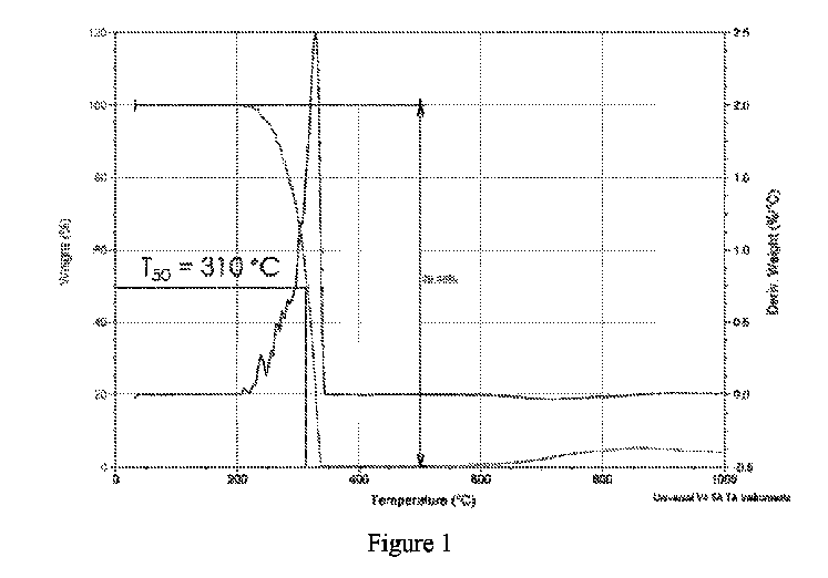
【選択図】図1
The present invention provides certain molybdenum-containing compounds believed to be useful for the deposition of molybdenum-containing films on the surfaces of various microelectronic device substrates. In one aspect, the present invention provides a method for depositing a molybdenum-containing film on a microelectronic device substrate, the method comprising exposing the substrate to a compound of formula (I) as described herein in a reaction zone under deposition conditions.
[Selected Figure] Figure 1
Description
優先権の主張
本発明は、2021年11月10日出願の米国仮特許出願第63/277,829号の優先権を主張する。本優先権文書は、参照により本明細書に組み込まれる。
CLAIM OF PRIORITY This invention claims priority to U.S. Provisional Patent Application No. 63/277,829, filed November 10, 2021. This priority document is incorporated herein by reference.
本発明は、マイクロ電子デバイス基板上へのモリブデン含有膜の蒸着における前駆体として有用なある特定のモリブデン化合物に関する。 The present invention relates to certain molybdenum compounds that are useful as precursors in the deposition of molybdenum-containing films on microelectronic device substrates.
モリブデン、クロム、およびタングステンなどの第6族の金属は、融点が極めて高く、熱膨張係数が小さく、抵抗率が低く、熱伝導率が高いという特徴から、拡散バリア、電極、フォトマスク、パワーエレクトロニクス基板、低抵抗ゲート、フラットパネルディスプレイ、および相互接続の使用を含む、半導体デバイスの製造にますます利用されている。 Group 6 metals such as molybdenum, chromium, and tungsten are increasingly being used in the fabrication of semiconductor devices, including for use as diffusion barriers, electrodes, photomasks, power electronics substrates, low resistance gates, flat panel displays, and interconnects, due to their extremely high melting points, low coefficients of thermal expansion, low resistivity, and high thermal conductivity.
このような有用性は、効率的な大量製造の操作に対応するために、堆積させた膜の高い適合性および高い堆積速度を特徴とする、このような用途のためのモリブデン、クロムおよびタングステン膜の堆積を達成する取組みの動機付けとなっている。このため、蒸着操作に有用な改良されたモリブデンおよびタングステンの供給試薬、およびこのような試薬を利用した改良された工程パラメータの開発が取り組まれている。 Such utility has motivated efforts to achieve deposition of molybdenum, chromium and tungsten films for such applications that are characterized by high compatibility of the deposited films and high deposition rates to accommodate efficient high volume manufacturing operations. This has led to the development of improved molybdenum and tungsten delivery reagents useful in deposition operations, and improved process parameters utilizing such reagents.
原子層堆積(ALD)法では、反応物質と前駆体分子とが交互のパルスで反応ゾーンに導入され、所望の化学組成の層が形成される。これらの前駆体は気体の形態でウエハに供給される。標準的な温度と圧力において気体である前駆体については、この方法が十分に確立されている。前駆体気体は成膜チャンバーに直接流入する。新しいインターコネクト材料へのトレンドは、より広範な前駆体のポートフォリオを必要とし、その多くは室温で液体または固体である。これらのALD前駆体は、十分な揮発性、熱安定性、および基板と堆積される膜との反応性を有していなければならない。液体であれ固体であれ、前駆体の蒸気圧がプロセス条件を決定する。 In atomic layer deposition (ALD) reactants and precursor molecules are introduced in alternating pulses into a reaction zone to form layers of the desired chemical composition. These precursors are delivered to the wafer in gaseous form. For precursors that are gaseous at standard temperatures and pressures, the method is well established. The precursor gas flows directly into the deposition chamber. The trend towards new interconnect materials requires a broader portfolio of precursors, many of which are liquids or solids at room temperature. These ALD precursors must have sufficient volatility, thermal stability, and reactivity with the substrate and the film being deposited. The vapor pressure of the precursor, whether liquid or solid, determines the process conditions.
ほとんどの液体前駆体は室温で供給され、圧力を下げることで気化する。一般に、液体は固体前駆体よりも精製、取り扱い、供給が容易である。したがって、多くの垂直統合型デバイスメーカー(IDM)は、液体供給装置を好む。 Most liquid precursors are delivered at room temperature and vaporized by reducing the pressure. Liquids are generally easier to purify, handle, and deliver than solid precursors. Therefore, many integrated device manufacturers (IDMs) prefer liquid delivery systems.
固体は、材料とそれを供給するガスラインを加熱する必要があるため、より困難である。理想的には、前駆体は不燃性、非腐食性、非毒性であり、製造が簡単で安価であるべきである。 Solids are more difficult because the material and the gas lines that supply it must be heated. Ideally, the precursor should be non-flammable, non-corrosive, non-toxic, and easy and cheap to produce.
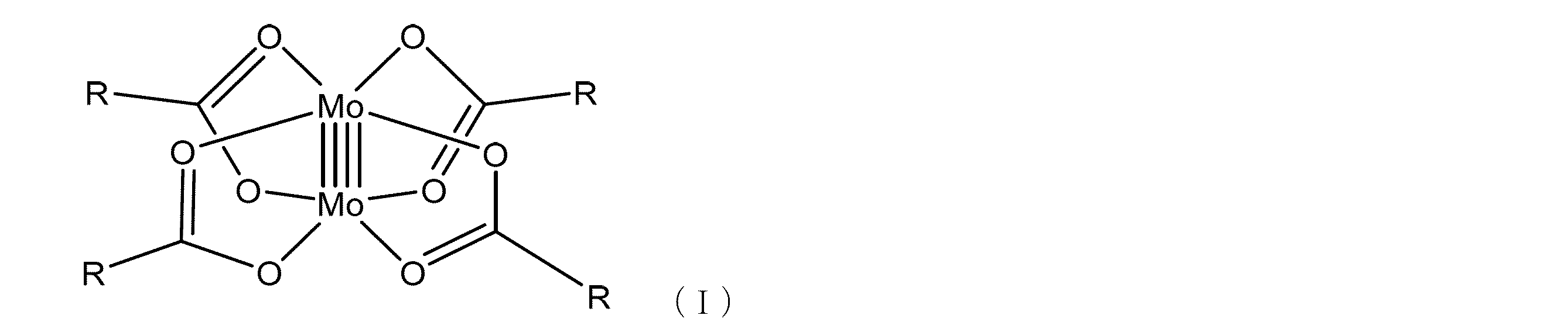
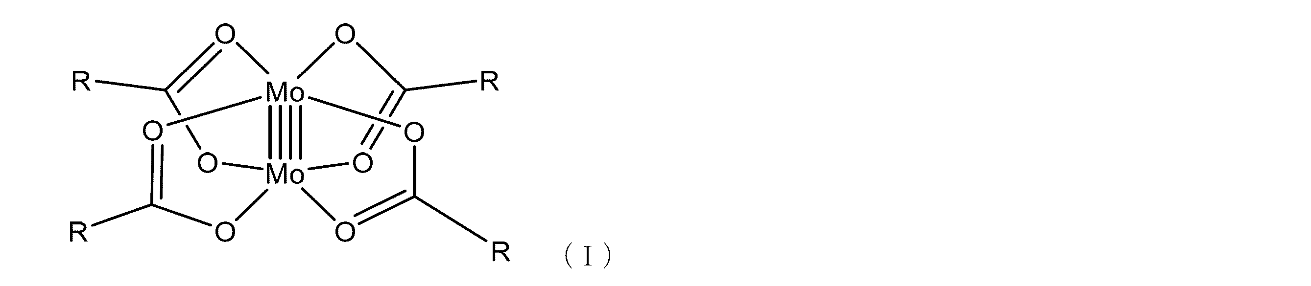
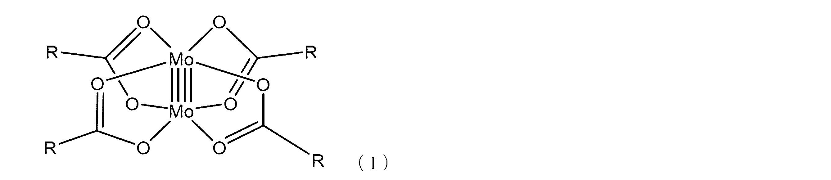
要約すると、本発明は、様々なマイクロエレクトロニクスデバイス基板の表面へのモリブデン含有膜の蒸着に有用であると考えられる、ある特定のモリブデン含有化合物を提供する。一態様では、本発明は、マイクロエレクトロニクスデバイス基板上にモリブデン含有膜を堆積させるための方法であって、反応ゾーンにおいて、蒸着条件下で、基板を式(I)の化合物:
に曝露することを含み、それによって基板上にモリブデン含有膜を形成する法を提供する。
In summary, the present invention provides certain molybdenum-containing compounds believed to be useful for the deposition of molybdenum-containing films on the surfaces of various microelectronic device substrates. In one aspect, the present invention provides a method for depositing a molybdenum-containing film on a microelectronic device substrate, comprising reacting the substrate with a compound of formula (I) in a reaction zone under deposition conditions:
to form a molybdenum-containing film on the substrate.
本明細書および添付の特許請求の範囲で使用される場合、単数形「1つの(a)」、「1つの(an)」および「その(the)」は、内容が明確に指示しない限り、複数の指示対象を含む。本明細書および添付の特許請求の範囲で使用される場合、用語「または」は、内容が明確に指示しない限り、一般に「および/または」を含む意味で使用される。 As used in this specification and the appended claims, the singular forms "a," "an," and "the" include plural referents unless the content clearly dictates otherwise. As used in this specification and the appended claims, the term "or" is generally used in its sense including "and/or" unless the content clearly dictates otherwise.
用語「約」は、一般に、言及された値と同等とみなされる(例えば、同じ機能または結果を有する)数値の範囲を指す。多くの場合、用語「約」は、最も近い有効数字に丸められる数値を含むことがある。 The term "about" generally refers to a range of numbers that are considered equivalent to the stated value (e.g., having the same function or result). In many cases, the term "about" may include numbers that are rounded to the nearest significant figure.
終点を使用して表現される数値範囲は、その範囲に包含されるすべての数値を含む(例えば、1~5は、1、1.5、2、2.75、3、3.80、4、5を含む)。 Numerical ranges expressed using endpoints include all numbers subsumed within that range (e.g., 1 to 5 includes 1, 1.5, 2, 2.75, 3, 3.80, 4, and 5).
第1の態様では、本発明は、マイクロエレクトロニクスデバイス基板上にモリブデン含有膜を堆積させる方法であって、反応ゾーンにおいて、基板を式(I)の化合物に曝露することを含む方法を提供する
蒸着条件下により、基板上にモリブデン含有膜が形成する]。
In a first aspect, the present invention provides a method for depositing a molybdenum-containing film on a microelectronic device substrate, the method comprising exposing the substrate in a reaction zone to a compound of formula (I):
Under deposition conditions, a molybdenum-containing film forms on the substrate.
一実施形態では、各Rは、メチル、tert-ブチル、およびトリフルオロメチルから選択される。 In one embodiment, each R is selected from methyl, tert-butyl, and trifluoromethyl.
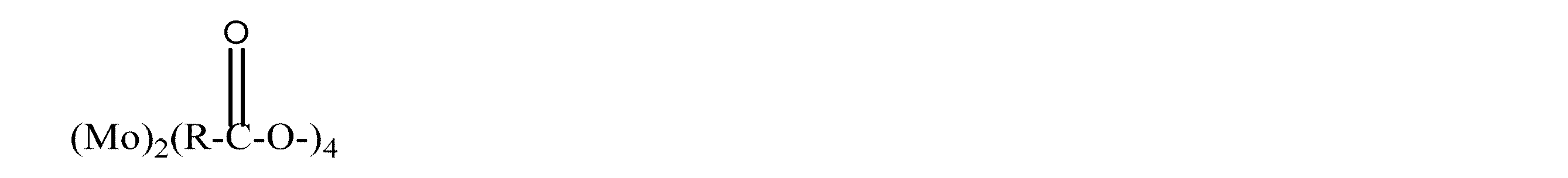
上に示した式(I)の化合物は、モリブデン含有アルカノエートのダイマーとして存在する。言い換えれば、式(I)の化合物は、経験式
を有する。
The compounds of formula (I) shown above exist as dimers of molybdenum-containing alkanoates. In other words, the compounds of formula (I) have the empirical formula
has.
式(I)の化合物の多くは公知であり、モリブデンヘキサカルボニル(Mo(CO)6)を酢酸で処理することによって調製することができる(すなわち、Rがメチルである場合)。同様に、式(I)の対応するR基には、他のカルボン酸を利用することができる。(例えば、Rhenium and Molybdenum Compounds Containing Quadruple Bonds、Alicia B.Brignole、F.A.Cotton、Z.Dori、Z.Dori、Z.Dori、G.Wilkinson;書籍編集者:F.A.Cotton;初版:1972年1月1日;https://doi.org/10.1002/9780470132449.ch15.を参照のこと。さらに、Rがメチルである場合、酢酸モリブデン(II)ダイマー化合物は、Sigma Aldrich(CAS番号14221-06-8)から商業的に入手できる。) Many of the compounds of formula (I) are known and can be prepared by treating molybdenum hexacarbonyl (Mo(CO) 6 ) with acetic acid (i.e., where R is methyl). Similarly, other carboxylic acids can be utilized for the corresponding R group of formula (I). (See, for example, Rhenium and Molybdenum Compounds Containing Quadruple Bonds, Alicia B. Brignole, F. A. Cotton, Z. Dori, Z. Dori, Z. Dori, G. Wilkinson; Book Editor: F. A. Cotton; First Edition: January 1, 1972; https://doi.org/10.1002/9780470132449.ch15. Additionally, when R is methyl, the molybdenum (II) acetate dimer compound is commercially available from Sigma Aldrich (CAS No. 14221-06-8).)
式(I)の化合物は、モリブデン含有膜の化学蒸着に有用であると考えられる。これに関して、用語「モリブデン含有」膜は、モリブデン金属、酸化モリブデン、炭化モリブデン、および窒化モリブデンのうちの1種または複数から構成される膜である。 The compounds of formula (I) are believed to be useful for the chemical vapor deposition of molybdenum-containing films. In this regard, the term "molybdenum-containing" films are films comprised of one or more of molybdenum metal, molybdenum oxide, molybdenum carbide, and molybdenum nitride.
化学的な蒸着法としては、化学的気相成長(CVD)法、および原子層堆積(ALD)法と称される方法が挙げられ、これらは、特に、UVレーザー光解離CVD、プラズマアシストCVD、パルスCVD、およびプラズマアシストALDなどのこれらのいくつかの派生バージョンも含む。二次元または三次元のマイクロエレクトロニクスデバイス基板上への高純度の金属の蒸着において、これらの種類の蒸着法は、蒸着された金属の純度が高く、多くの場合、非常に非平面的なマイクロエレクトロニクスデバイス形状に良好なコンフォーマルな段差被覆性を与えることができるため、望ましいことがある。 Chemical vapor deposition techniques include those referred to as chemical vapor deposition (CVD) and atomic layer deposition (ALD), including several derivative versions thereof, such as UV laser photodissociation CVD, plasma-assisted CVD, pulsed CVD, and plasma-assisted ALD, among others. In the deposition of high purity metals onto two-dimensional or three-dimensional microelectronic device substrates, these types of deposition techniques can be desirable due to the high purity of the deposited metal and the ability to provide good conformal step coverage on the often highly non-planar microelectronic device geometries.
一実施形態では、基板表面上に堆積されるモリブデン含有膜または層は、例えば、化学気相成長、パルス化学気相成長(CVD)または原子層堆積(ALD)によって、したがって式(I)の化合物から誘導される蒸気を直接用いて形成することができる。 In one embodiment, the molybdenum-containing film or layer deposited on the substrate surface can be formed, for example, by chemical vapor deposition, pulsed chemical vapor deposition (CVD) or atomic layer deposition (ALD), thus directly using vapor derived from the compound of formula (I).
一実施形態では、式(I)の化合物を、還元性ガスと共に、マイクロエレクトロニクスデバイス基板を含有する反応ゾーンに導入する。反応ゾーンの条件は、式(I)の前駆体中に含有するモリブデンがモリブデン金属としてマイクロエレクトロニクスデバイス基板上に堆積するように選択する。一実施形態では、前駆体および還元性ガスを反応ゾーンに連続的に導入する。別の実施形態では、堆積金属層の組成を改善するために、酸素、オゾン、または水と水素とを組み合わせたものなどの酸化性ガスを反応ゾーンに導入することができる。したがって、酸化性ガスは、完成したモリブデン層中に堆積する炭素の量を減少させる量および方式で導入する。一実施形態では、この酸化性ガスは、パルス状で断続的に導入する。この技法のさらなる詳細については、参照により本明細書に組み込まれる米国特許公開第2020/0115798号で見出すことができる。 In one embodiment, the compound of formula (I) is introduced together with a reducing gas into a reaction zone containing a microelectronic device substrate. The conditions in the reaction zone are selected such that the molybdenum contained in the precursor of formula (I) is deposited on the microelectronic device substrate as molybdenum metal. In one embodiment, the precursor and the reducing gas are introduced continuously into the reaction zone. In another embodiment, an oxidizing gas, such as oxygen, ozone, or a combination of water and hydrogen, can be introduced into the reaction zone to improve the composition of the deposited metal layer. Thus, the oxidizing gas is introduced in an amount and manner that reduces the amount of carbon that is deposited in the completed molybdenum layer. In one embodiment, the oxidizing gas is introduced intermittently in a pulsed manner. Further details of this technique can be found in U.S. Patent Publication No. 2020/0115798, which is incorporated herein by reference.
したがって、一実施形態では、本発明は、マイクロエレクトロニクスデバイス基板上にモリブデン含有膜を堆積させるための方法であって、式(I)の前駆体をマイクロエレクトロニクスデバイス基板を含有する反応ゾーンに導入し、同時に反応ゾーンに還元性ガスを導入することを含む方法を提供する。別の実施形態では、本方法は、反応ゾーンに酸化性ガスのパルスを断続的に導入する工程をさらに含む。 Thus, in one embodiment, the present invention provides a method for depositing a molybdenum-containing film on a microelectronic device substrate, comprising introducing a precursor of formula (I) into a reaction zone containing the microelectronic device substrate and simultaneously introducing a reducing gas into the reaction zone. In another embodiment, the method further comprises intermittently introducing pulses of an oxidizing gas into the reaction zone.
別の実施形態では、式(I)のモリブデン前駆体を、マイクロエレクトロニクスデバイス基板を含有する反応ゾーンに導入し、続いて酸化性ガス(例えば、H2O蒸気)をパルス導入し、続いて還元性ガス(例えば、H2)をパルス導入することができる。このようにして、モリブデン金属膜をマイクロエレクトロニクスデバイス基板の表面に堆積させることができる。したがって、さらなる実施形態では、本発明は、マイクロエレクトロニクスデバイス基板上にモリブデン含有膜を堆積させるための方法であって、(i)式(I)の前駆体を、マイクロエレクトロニクスデバイス基板を含有する反応ゾーンに導入し、その間、断続的に(ii)基板を酸化性ガスに曝露し;断続的に(iii)基板を還元性ガスに曝露することを含む方法を提供する。ある特定の実施形態では、前駆体、酸化性ガス、および還元性ガスは、原子層堆積領域にパルスで導入される。 In another embodiment, a molybdenum precursor of formula (I) can be introduced into a reaction zone containing a microelectronic device substrate, followed by a pulse of an oxidizing gas (e.g., H2O vapor), followed by a pulse of a reducing gas (e.g., H2 ). In this manner, a molybdenum metal film can be deposited on the surface of a microelectronic device substrate. Thus, in a further embodiment, the present invention provides a method for depositing a molybdenum-containing film on a microelectronic device substrate, comprising: (i) introducing a precursor of formula (I) into a reaction zone containing a microelectronic device substrate, while intermittently (ii) exposing the substrate to an oxidizing gas; and intermittently (iii) exposing the substrate to a reducing gas. In certain embodiments, the precursor, the oxidizing gas, and the reducing gas are pulsed into the atomic layer deposition region.
本発明のある特定の実施形態では、酸化性ガスは、H2O蒸気、H2O2、O3、およびN2Oから選択されるガスで構成される。本発明のある特定の実施形態では、還元性ガスは、H2、ヒドラジン(N2H4)、メチルヒドラジン、t-ブチルヒドラジン、1,1-ジメチルヒドラジン、1,2-ジメチルヒドラジン、およびNH3から選択されるガスで構成される。H2O2およびO3の酸化電位を考慮すると、このようなガスは、ヒドラジン(N2H4)、メチルヒドラジン、t-ブチルヒドラジン、1,1-ジメチルヒドラジン、もしくは1,2-ジメチルヒドラジンと共に利用すべきではないこと、または順次利用する場合は、基質を他の反応物質に曝露する前に、このような工程から残存するこのようなあらゆるガスを反応器からパージすべきであることが理解されよう。これらの技法に関するさらなる詳細については、参照により本明細書に組み込まれる米国特許公開第2021/062331号で見出すことができる。 In certain embodiments of the invention, the oxidizing gas is comprised of a gas selected from H 2 O vapor, H 2 O 2 , O 3 , and N 2 O. In certain embodiments of the invention, the reducing gas is comprised of a gas selected from H 2 , hydrazine (N 2 H 4 ), methylhydrazine, t-butylhydrazine, 1,1-dimethylhydrazine, 1,2-dimethylhydrazine, and NH 3. Given the oxidation potentials of H 2 O 2 and O 3 , it will be understood that such gases should not be utilized with hydrazine (N 2 H 4 ), methylhydrazine, t-butylhydrazine, 1,1-dimethylhydrazine, or 1,2-dimethylhydrazine, or if utilized sequentially, any such gas remaining from such steps should be purged from the reactor prior to exposing the substrate to the other reactant. Further details regarding these techniques can be found in U.S. Patent Publication No. 2021/062331, which is incorporated herein by reference.
ある特定の場合では、アンモニア(NH3)、ヒドラジン(N2H4);メチルヒドラジン、t-ブチルヒドラジン、1,1-ジメチルヒドラジン、および1,2-ジメチルヒドラジンなどのC1~C4アルキルヒドラジンなどの窒素含有還元性ガスは有用であり得るが、一部の条件下では純粋な金属膜ではなくモリブデン含有窒化物膜がもたらされる。同様に、ある特定の実施形態では、一酸化炭素、アルカン、アルケン、およびアルキンなどの炭素含有還元性ガスは有用であり得るが、一部の条件下では、純粋な金属膜ではなく炭化モリブデン膜がもたらされる。一実施形態では、還元性ガスは水素である。 In certain cases, nitrogen-containing reducing gases such as ammonia (NH 3 ), hydrazine (N 2 H 4 ); C 1 -C 4 alkyl hydrazines such as methylhydrazine, t-butylhydrazine, 1,1-dimethylhydrazine, and 1,2-dimethylhydrazine may be useful, but under some conditions will result in molybdenum-containing nitride films rather than pure metal films. Similarly, in certain embodiments, carbon-containing reducing gases such as carbon monoxide, alkanes, alkenes, and alkynes may be useful, but under some conditions will result in molybdenum carbide films rather than pure metal films. In one embodiment, the reducing gas is hydrogen.
本明細書に開示される方法は、金属前駆体と還元性ガスおよび/または酸化性ガス、ならびにキャリアガスの導入の間の任意選択の工程として、1種または複数のパージガスを含むことができる。未消費の反応物質および/もしくは反応副生成物をパージ除去するか、または金属前駆体および還元性ガスもしくは酸化性ガスの希釈剤およびキャリアとして機能するかのいずれかのために使用されるパージガスまたはキャリアガスは、前駆体と反応しない不活性ガスである。例示的なガスとしては、アルゴン、窒素、ヘリウム、ネオン、およびそれらの混合物が挙げられるが、これらに限定されない。ある特定の実施形態では、Arなどのパージガスは、約10~約10000sccmの範囲の流量で、約0.1~1000秒間、反応器内に供給され、それによって未反応物質および反応器内に残存し得るあらゆる副生成物をパージする。その他、このような不活性ガスは、本明細書で使用されるように、反応ゾーンに注入されるモリブデン前駆体ならびに/または酸化性ガスおよび/もしくは還元性ガスの濃度を変化させるためのキャリアガスとして利用することができる。キャリアガスの利用およびその流量は、最終的には、堆積ツールの構成、その操作規模、および利用される特定の前駆体に依存する。 The methods disclosed herein may include one or more purge gases as an optional step between the introduction of the metal precursor and the reducing and/or oxidizing gases, and the carrier gas. The purge or carrier gas, used either to purge out unconsumed reactants and/or reaction by-products, or to act as a diluent and carrier for the metal precursor and the reducing or oxidizing gas, is an inert gas that does not react with the precursor. Exemplary gases include, but are not limited to, argon, nitrogen, helium, neon, and mixtures thereof. In certain embodiments, a purge gas, such as Ar, is fed into the reactor at a flow rate ranging from about 10 to about 10,000 sccm for about 0.1 to 1000 seconds, thereby purging unreacted materials and any by-products that may remain in the reactor. Other such inert gases, as used herein, may be utilized as carrier gases to vary the concentration of the molybdenum precursor and/or the oxidizing and/or reducing gas injected into the reaction zone. The use of carrier gas and its flow rate will ultimately depend on the configuration of the deposition tool, its scale of operation, and the particular precursors being utilized.
一実施形態では、元素モリブデン含有膜の形成をもたらすために、式(I)の前駆体と共に還元性ガスを利用することができる。あるいは、MoO2などの金属酸化物薄膜を堆積させる手段として本明細書に記載の前駆体を使用する場合、酸素などの酸化性ガス(すなわち、共反応物質)を本方法に加えることができる。 In one embodiment, a reducing gas can be utilized with the precursor of formula (I) to effect the formation of an elemental molybdenum-containing film. Alternatively, when using the precursors described herein as a means to deposit metal oxide thin films such as MoO2 , an oxidizing gas such as oxygen (i.e., a co-reactant) can be added to the method.
多様な実施形態では、蒸着条件は、任意選択のそのような還元性ガスおよび/または酸化性ガスの存在を除けば、不活性雰囲気を含む。ある特定の実施形態では、前駆体蒸気は、他の金属蒸気の実質的な非存在下で堆積することができる。 In various embodiments, deposition conditions include an inert atmosphere, except for the optional presence of such reducing and/or oxidizing gases. In certain embodiments, the precursor vapor can be deposited in the substantial absence of other metal vapors.
ある特定の実施形態では、基板表面上に堆積されるモリブデン含有層は、例えば、核形成層を事前に形成することなく、化学気相成長(CVD)法、パルス化学気相成長法、原子層堆積(ALD)法、または他の(熱的)気相成長法によって形成することができる。それぞれの前駆体蒸気接触工程は、モリブデン含有膜の所望の厚さを形成させるために所望のサイクル数だけ交互に繰り返し実施することができる。多様な実施形態では、基板(例えば、窒化チタン)層と式(I)の化合物蒸気との接触は、このような蒸着に対して200℃~750℃の範囲の温度で、約0.5~約500Torrの圧力で行われる。式(I)の化合物、還元性ガス、および酸化性ガスのパルス導入は、ある特定の実施形態において、約0.2秒~約60秒の持続時間の範囲であることができる。 In certain embodiments, the molybdenum-containing layer deposited on the substrate surface can be formed, for example, by chemical vapor deposition (CVD), pulsed chemical vapor deposition, atomic layer deposition (ALD), or other (thermal) vapor deposition methods without the prior formation of a nucleation layer. Each precursor vapor contact step can be alternately repeated for a desired number of cycles to form a desired thickness of the molybdenum-containing film. In various embodiments, the contact of the substrate (e.g., titanium nitride) layer with the vapor of the compound of formula (I) is performed at a temperature ranging from 200° C. to 750° C. for such deposition, and at a pressure of about 0.5 to about 500 Torr. The pulse introduction of the compound of formula (I), the reducing gas, and the oxidizing gas can range in duration from about 0.2 seconds to about 60 seconds in certain embodiments.
モリブデン金属含有材料は、上述のように、モリブデン金属、酸化物、炭化物、または窒化物のバルク堆積物を形成させるために、基板上に直接堆積することができる。元素モリブデン膜の堆積が望まれ、かつH2が還元性ガスとして利用される場合、金属形成には、4モル当量を超えるH2、または過剰のH2が必要であるため、H2の濃度は、モリブデン金属対酸化物の形成に対して重要である。4モル当量未満のH2では、様々な量のモリブデン金属の酸化物が形成され、したがって、こうして形成された酸化モリブデンを還元するために、H2にさらに曝露する必要がある。 Molybdenum metal-containing materials can be directly deposited on a substrate to form bulk deposits of molybdenum metal, oxide, carbide, or nitride, as described above. When deposition of elemental molybdenum films is desired and H2 is utilized as the reducing gas, the concentration of H2 is important to the formation of molybdenum metal vs. oxide, since metal formation requires more than 4 molar equivalents of H2 , or excess H2 . Below 4 molar equivalents of H2 , various amounts of molybdenum metal oxides are formed, and therefore further exposure to H2 is required to reduce the molybdenum oxide thus formed.
本開示に従ってこのようなモリブデン含有材料を堆積させるためのプロセス化学は、反応Mo2(O2CCH3)4+2H2→2Mo+4HOCCH3によって元素モリブデン、Mo(0)の堆積を含むことができる。中間的な反応は、存在してもよく、当該技術分野では周知である。 Process chemistries for depositing such molybdenum-containing materials in accordance with the present disclosure can include the deposition of elemental molybdenum, Mo(0), via the reaction Mo2 ( O2CCH3 ) 4 + 2H2 → 2Mo + 4HOCCH3. Intermediate reactions may exist and are well known in the art.
本発明の方法に従って堆積されたモリブデン含有材料は、モリブデン含有材料の堆積速度、堆積されたモリブデン含有材料の膜抵抗率、堆積されたモリブデン含有材料の膜形態、堆積されたモリブデン含有材料の膜応力、材料の段差被覆性、膜組成および純度、ならびに適切なプロセス条件のプロセスウィンドウまたはプロセスエンベロープ(process envelope)などの任意の適切な評価指標およびパラメータによって特徴付けることができる。任意の適切な評価指標およびパラメータを採用して、堆積材料を特徴付けて、これを特定のプロセス条件に関連付けることにより、対応する半導体製品およびフラットパネルディスプレイの大量生産を可能にすることができる。有利なことに、本発明の方法は、マイクロエレクトロニクスデバイス基板上に高純度のモリブデン金属の膜を堆積させることができると考えられる。 The molybdenum-containing material deposited according to the method of the present invention can be characterized by any suitable metrics and parameters, such as the deposition rate of the molybdenum-containing material, the film resistivity of the deposited molybdenum-containing material, the film morphology of the deposited molybdenum-containing material, the film stress of the deposited molybdenum-containing material, the step coverage of the material, the film composition and purity, and the process window or process envelope of suitable process conditions. Any suitable metrics and parameters can be employed to characterize the deposited material and relate it to specific process conditions to enable mass production of corresponding semiconductor products and flat panel displays. Advantageously, it is believed that the method of the present invention can deposit a film of high purity molybdenum metal on a microelectronic device substrate.
本発明の堆積方法で利用される基板は、任意の好適な種類のものであることができ、例えば、マイクロエレクトロニクスデバイス基板、例えば、シリコン基板、二酸化シリコン基板、または他のシリコンベースの基板を含むことができる。多様な実施形態では、基板は、1種または複数の金属基板または誘電体基板、例えば、Co、Cu、Al、W、WN、WC、TiN、Mo、MoC、SiO2、W、SiN、WCN、Al2O3、AlN、ZrO2、HfO2、SiO2、酸化ランタン(La2O3)、窒化タンタル(TaN)、窒化ニオブ、酸化ルテニウム(RuO2)、酸化イリジウム(IrO2)、酸化ニオブ(Nb2O3)、酸化イットリウム(Y2O3)を含むことができる。 The substrate utilized in the deposition method of the present invention can be of any suitable type and can include, for example, a microelectronic device substrate, such as a silicon substrate, a silicon dioxide substrate, or other silicon-based substrate. In various embodiments, the substrate can include one or more metal or dielectric substrates, such as Co, Cu, Al, W, WN, WC, TiN, Mo, MoC, SiO2 , W, SiN, WCN , Al2O3 , AlN, ZrO2 , HfO2, SiO2 , lanthanum oxide ( La2O3 ), tantalum nitride (TaN), niobium nitride, ruthenium oxide ( RuO2 ), iridium oxide ( IrO2 ), niobium oxide (Nb2O3), yttrium oxide ( Y2O3 ).
ある特定の実施形態では、例えば、二酸化ケイ素などの酸化物基板の場合、またはその代わりにシリコン基板もしくはポリシリコン基板の場合、基板は、その後に堆積される材料のために、その上に窒化チタンなどのバリア層を含むように加工または製造することができる。 In certain embodiments, for example in the case of an oxide substrate such as silicon dioxide, or alternatively in the case of a silicon or polysilicon substrate, the substrate can be processed or manufactured to include a barrier layer thereon, such as titanium nitride, for the subsequently deposited material.
本発明の方法は、多数の代替的な方法で、多種多様なプロセス条件下で実施できることが理解されよう。マイクロエレクトロニクスまたは半導体デバイスは、任意の好適な種類のものであることができ、例えば、DRAMデバイス、3-D NANDデバイス、または他のデバイス、すなわちデバイス集積構造を含むことができる。多様な実施形態では、基板は、モリブデン含有材料が堆積されるビアを含むことができる。デバイスは、例えば、10:1~40:1の範囲にある深さ対横寸法のアスペクト比を有することができる。他の実施形態では、本方法は、モバイルデバイス、ロジックデバイス、フラットパネルディスプレイ、またはICパッケージング部品などのマイクロエレクトロニクスデバイス製品の製造において実施することができる。 It will be appreciated that the method of the present invention can be practiced in many alternative ways and under a wide variety of process conditions. The microelectronic or semiconductor device can be of any suitable type and can include, for example, DRAM devices, 3-D NAND devices, or other devices, i.e., device integration structures. In various embodiments, the substrate can include vias into which the molybdenum-containing material is deposited. The device can have an aspect ratio of depth to lateral dimension, for example, in the range of 10:1 to 40:1. In other embodiments, the method can be practiced in the manufacture of microelectronic device products, such as mobile devices, logic devices, flat panel displays, or IC packaging components.
本発明の方法では、前駆体化合物は、任意の好適な方法で、例えば、単一ウエハチャンバー、マルチウエハチャンバー内、または複数のウエハを含有する炉内で、所望のマイクロエレクトロニクスデバイス表面または基板と反応することができる。 In the methods of the present invention, the precursor compounds can be reacted with the desired microelectronic device surface or substrate in any suitable manner, for example, in a single wafer chamber, a multi-wafer chamber, or in a furnace containing multiple wafers.
本明細書で使用される場合、用語「マイクロエレクトロニクスデバイス」は、マイクロエレクトロニクス、集積回路、またはコンピュータチップの用途で使用するために製造される、3D NAND構造、ロジックデバイス、DRAM、パワーデバイス、フラットパネルディスプレイ、および微小電気機械システム(MEMS)を含む半導体基板に対応する。用語「マイクロエレクトロニクスデバイス」は、いかなる意味においても限定的なものではなく、n型チャネル金属酸化物半導体(nMOS)および/またはp型チャネル金属酸化物半導体(pMOS)トランジスタを含み、最終的にマイクロエレクトロニクスデバイスまたはマイクロエレクトロニクスアセンブリとなるあらゆる基板を含むことを理解されたい。さらに、下地基板はシリコンである必要はなく、ガラスもしくはサファイアなどの絶縁体、SiCもしくはGaNなどの高いバンドギャップ半導体、または電気回路の製造に有用な他の材料であることができる。このようなマイクロエレクトロニクスデバイスは、少なくとも1つの基板を含有し、この基板は、例えば、シリコン、SiO2、Si3N4、OSG、FSG、炭化ケイ素、水素化炭化ケイ素、窒化ケイ素、水素化窒化ケイ素、炭窒化ケイ素、水素化炭窒化ケイ素、窒化ホウ素、反射防止コーティング、フォトレジスト、ゲルマニウム、ゲルマニウム含有、ホウ素含有、Ga/As、フレキシブル基板、多孔質無機材料、銅およびアルミニウムなどの金属、ならびにTiN、Ti(C)N、TaN、Ta(C)N、Ta、W、WNなどの拡散バリア層が挙げられるが、これらに限定されないものから選択することができる。膜は、例えば、化学機械平坦化(chemical mechanical planarization)(CMP)および異方性エッチングプロセスなどの様々な後続処理工程に適合する。 As used herein, the term "microelectronic device" corresponds to a semiconductor substrate, including 3D NAND structures, logic devices, DRAM, power devices, flat panel displays, and microelectromechanical systems (MEMS), that is manufactured for use in microelectronic, integrated circuit, or computer chip applications. It is to be understood that the term "microelectronic device" is not limiting in any way and includes any substrate that contains n-channel metal oxide semiconductor (nMOS) and/or p-channel metal oxide semiconductor (pMOS) transistors and that will ultimately become a microelectronic device or microelectronic assembly. Furthermore, the underlying substrate need not be silicon, but can be an insulator such as glass or sapphire, a high bandgap semiconductor such as SiC or GaN, or other materials useful in the manufacture of electrical circuits. Such microelectronic devices contain at least one substrate, which may be selected from, for example, but not limited to, silicon, SiO 2 , Si 3 N 4 , OSG, FSG, silicon carbide, hydrogenated silicon carbide, silicon nitride, hydrogenated silicon nitride, silicon carbonitride, hydrogenated silicon carbonitride, boron nitride, anti-reflective coatings, photoresist, germanium, germanium-containing, boron-containing, Ga/As, flexible substrates, porous inorganic materials, metals such as copper and aluminum, and diffusion barrier layers such as TiN, Ti(C)N, TaN, Ta(C)N, Ta, W, WN, etc. The films are compatible with various subsequent processing steps, such as, for example, chemical mechanical planarization (CMP) and anisotropic etching processes.
態様
第1の態様では、本発明は、マイクロエレクトロニクスデバイス基板上にモリブデン含有膜を堆積させるための方法であって、反応ゾーンにおいて、基板を式(I)の化合物に曝露することを含む方法を提供する

蒸着条件下により、基板上にモリブデン含有膜が形成する]。
In a first aspect, the present invention provides a method for depositing a molybdenum-containing film on a microelectronic device substrate, the method comprising exposing the substrate in a reaction zone to a compound of formula (I):
Under deposition conditions, a molybdenum-containing film forms on the substrate.
第2の態様では、本発明は、各RがC1~C4アルキルである、第1の態様の方法を提供する。 In a second aspect, the present invention provides the method of the first aspect, wherein each R is C 1 -C 4 alkyl.
第3の態様では、本発明は、各Rがメチルである、第1の態様の方法を提供する。 In a third aspect, the present invention provides the method of the first aspect, wherein each R is methyl.
第4の態様では、本発明は、各Rがtert-ブチルである、第1または第2の態様の方法を提供する。 In a fourth aspect, the present invention provides the method of the first or second aspect, wherein each R is tert-butyl.
第5の態様では、本発明は、各Rがトリフルオロメチルである、第1の態様の方法を提供する。 In a fifth aspect, the present invention provides the method of the first aspect, wherein each R is trifluoromethyl.
第6の態様では、本発明は、蒸着条件が、約200℃~約750℃の温度および約0.5~約500Torrの圧力を含む、第1から第5の態様のいずれか1つの方法を提供する。 In a sixth aspect, the present invention provides a method of any one of the first to fifth aspects, wherein the deposition conditions include a temperature of about 200° C. to about 750° C. and a pressure of about 0.5 to about 500 Torr.
第7の態様では、本発明は、蒸着条件が、マイクロエレクトロニクスデバイス基板を含有する反応ゾーンに式(I)の化合物を導入し、同時に還元性ガスを反応ゾーンに導入することを含む、第1から第6の態様のいずれか1つの方法を提供する。 In a seventh aspect, the invention provides a method of any one of the first to sixth aspects, wherein the deposition conditions include introducing a compound of formula (I) into a reaction zone containing a microelectronic device substrate and simultaneously introducing a reducing gas into the reaction zone.
第8の態様では、本発明は、蒸着条件が、反応ゾーンに酸化性ガスのパルスを断続的に導入する工程をさらに含む、第7の態様の方法を提供する。 In an eighth aspect, the present invention provides the method of the seventh aspect, wherein the deposition conditions further comprise intermittently introducing pulses of an oxidizing gas into the reaction zone.
第9の態様では、本発明は、蒸着条件が、(i)マイクロエレクトロニクスデバイス基板を含有する反応ゾーンに式(I)の前駆体を導入し、その間断続的に(ii)基板を酸化性ガスに曝露し;断続的に(iii)基板を還元性ガスに曝露することを含む、第1から第6の態様のいずれか1つの方法を提供する。 In a ninth aspect, the invention provides the method of any one of the first to sixth aspects, wherein the deposition conditions include (i) introducing a precursor of formula (I) into a reaction zone containing a microelectronic device substrate while intermittently (ii) exposing the substrate to an oxidizing gas; and intermittently (iii) exposing the substrate to a reducing gas.
第10の態様では、本発明は、還元性ガスが、H2、ヒドラジン、メチルヒドラジン、t-ブチルヒドラジン、1,2-ジメチルヒドラジン、1,2-ジメチルヒドラジン、およびNH3から選択されるガスから構成される、第7または第9の態様の方法を提供する。 In a tenth aspect, the present invention provides a method of the seventh or ninth aspects, wherein the reducing gas consists of a gas selected from H2 , hydrazine, methylhydrazine, t-butylhydrazine, 1,2-dimethylhydrazine, 1,2-dimethylhydrazine, and NH3 .
第11の態様では、本発明は、酸化性ガスが、H2O(H20)蒸気、H2O2、O3、およびN2Oから選択される、第8または第9の態様の方法を提供する。 In an eleventh aspect, the present invention provides a method of the eighth or ninth aspect, wherein the oxidizing gas is selected from H2O ( H2O ) vapor , H2O2 , O3 , and N2O .
第12の態様では、本発明は、基板が、窒化チタン、窒化タンタル、窒化アルミニウム、酸化アルミニウム、酸化ジルコニウム、酸化ハフニウム、二酸化ケイ素、窒化ケイ素、酸化ランタン、酸化ルテニウム、酸化イリジウム、酸化ニオブ、および酸化イットリウムから選択される、第1から第11の態様のいずれか1つの方法を提供する。 In a twelfth aspect, the present invention provides the method of any one of the first to eleventh aspects, wherein the substrate is selected from titanium nitride, tantalum nitride, aluminum nitride, aluminum oxide, zirconium oxide, hafnium oxide, silicon dioxide, silicon nitride, lanthanum oxide, ruthenium oxide, iridium oxide, niobium oxide, and yttrium oxide.
第13の態様では、本発明は、モリブデン含有膜がモリブデン金属である、第1から第12の態様のいずれか1つの方法を提供する。 In a thirteenth aspect, the present invention provides the method of any one of the first to twelfth aspects, wherein the molybdenum-containing film is molybdenum metal.
したがって、本開示のいくつかの例示的な実施形態について説明してきたが、当業者であれば、本明細書に添付した特許請求の範囲内で、さらに他の実施形態を作製し、使用することができることを容易に理解するであろう。本文書が対象とする本開示の多数の利点が、前述の説明において記載された。しかし、本開示は、多くの点で、例示に過ぎないことが理解されよう。もちろん、本開示の範囲は、添付の特許請求の範囲が表現する言語において表現される。 Thus, while several illustrative embodiments of the present disclosure have been described, those skilled in the art will readily appreciate that still other embodiments can be made and used within the scope of the claims appended hereto. Many advantages of the disclosure to which this document is directed have been set forth in the foregoing description. It will be understood, however, that the disclosure is, in many respects, only illustrative. The scope of the present disclosure will, of course, be expressed in the language of the appended claims.
Claims (13)
に曝露することを含み、それによって基板上にモリブデン含有膜を形成する方法。 1. A method for depositing a molybdenum-containing film on a microelectronic device substrate, comprising: reacting a compound of formula (I):
thereby forming a molybdenum-containing film on the substrate.
Applications Claiming Priority (3)
| Application Number | Priority Date | Filing Date | Title |
|---|---|---|---|
| US202163277829P | 2021-11-10 | 2021-11-10 | |
| US63/277,829 | 2021-11-10 | ||
| PCT/US2022/049145 WO2023086298A1 (en) | 2021-11-10 | 2022-11-07 | Molybdenum precursor compounds |
Publications (1)
| Publication Number | Publication Date |
|---|---|
| JP2024544133A true JP2024544133A (en) | 2024-11-28 |
Family
ID=86229652
Family Applications (1)
| Application Number | Title | Priority Date | Filing Date |
|---|---|---|---|
| JP2024527439A Pending JP2024544133A (en) | 2021-11-10 | 2022-11-07 | Molybdenum Precursor Compounds |
Country Status (7)
| Country | Link |
|---|---|
| US (1) | US12297531B2 (en) |
| EP (1) | EP4430226A4 (en) |
| JP (1) | JP2024544133A (en) |
| KR (1) | KR20240096719A (en) |
| CN (1) | CN118318063A (en) |
| TW (1) | TWI847351B (en) |
| WO (1) | WO2023086298A1 (en) |
Citations (3)
| Publication number | Priority date | Publication date | Assignee | Title |
|---|---|---|---|---|
| JPS62142779A (en) * | 1985-12-18 | 1987-06-26 | Canon Inc | Formation of deposited film |
| JP2019220254A (en) * | 2018-06-15 | 2019-12-26 | 宇部興産株式会社 | Lithium titanate powder for electrode of power storage device, material of active substance, electrode sheet arranged by use thereof, and power storage device |
| WO2020185618A1 (en) * | 2019-03-11 | 2020-09-17 | Lam Research Corporation | Precursors for deposition of molybdenum-containing films |
Family Cites Families (17)
| Publication number | Priority date | Publication date | Assignee | Title |
|---|---|---|---|---|
| GB2204065A (en) * | 1987-02-10 | 1988-11-02 | Plessey Co Plc | Vapour deposited metal films for integrated circuit manufacture |
| DE69025252T2 (en) * | 1989-09-26 | 1996-07-04 | Canon Kk | Method of manufacturing a deposited layer and method of manufacturing a semiconductor device |
| KR101525375B1 (en) * | 2008-04-28 | 2015-06-09 | 다이니폰 인사츠 가부시키가이샤 | Material for forming hole injection/transport layer and method for manufacturing the same |
| WO2010114386A1 (en) * | 2009-03-30 | 2010-10-07 | Universitetet I Oslo | Thin films containing molybdenum oxide |
| US8555402B2 (en) * | 2012-01-26 | 2013-10-08 | Microsoft Corporation | Dynamic selection of authorization processes |
| US9175023B2 (en) * | 2012-01-26 | 2015-11-03 | Sigma-Aldrich Co. Llc | Molybdenum allyl complexes and use thereof in thin film deposition |
| DE102012209520A1 (en) * | 2012-06-06 | 2013-12-12 | Osram Opto Semiconductors Gmbh | Metal complexes as p-dopants for organic electronic matrix materials |
| KR102149490B1 (en) * | 2012-11-19 | 2020-08-28 | 가부시키가이샤 아데카 | Method for producing thin film containing molybdenum, thin film-forming starting material, and molybdenum imide compound |
| WO2014140672A1 (en) * | 2013-03-15 | 2014-09-18 | L'air Liquide, Societe Anonyme Pour I'etude Et I'exploitation Des Procedes Georges Claude | Bis(alkylimido)-bis(alkylamido)molybdenum molecules for deposition of molybdenum-containing films |
| FR3016889B1 (en) * | 2014-01-24 | 2016-01-22 | Commissariat Energie Atomique | PROCESS FOR REASLISTING BY ALD A THIN LAYER OF MYX FORMULA |
| EP3417087A1 (en) * | 2016-02-19 | 2018-12-26 | Merck Patent GmbH | Deposition of molybdenum thin films using a molybdenum carbonyl precursor |
| US10510590B2 (en) * | 2017-04-10 | 2019-12-17 | Lam Research Corporation | Low resistivity films containing molybdenum |
| US11761081B2 (en) | 2018-10-10 | 2023-09-19 | Entegris, Inc. | Methods for depositing tungsten or molybdenum films |
| US20200131628A1 (en) | 2018-10-24 | 2020-04-30 | Entegris, Inc. | Method for forming molybdenum films on a substrate |
| KR102355507B1 (en) * | 2018-11-14 | 2022-01-27 | (주)디엔에프 | Method of manufacturing a molybdenum-containing thin film and molybdenum-containing thin film manufactured thereby |
| JP2022513903A (en) | 2018-12-19 | 2022-02-09 | インテグリス・インコーポレーテッド | A method of depositing a tungsten or molybdenum layer in the presence of a reducing co-reactant |
| WO2021041442A1 (en) | 2019-08-26 | 2021-03-04 | Entegris, Inc. | Group vi metal deposition process |
-
2022
- 2022-11-07 JP JP2024527439A patent/JP2024544133A/en active Pending
- 2022-11-07 CN CN202280079048.9A patent/CN118318063A/en active Pending
- 2022-11-07 EP EP22893503.7A patent/EP4430226A4/en active Pending
- 2022-11-07 US US17/982,220 patent/US12297531B2/en active Active
- 2022-11-07 WO PCT/US2022/049145 patent/WO2023086298A1/en not_active Ceased
- 2022-11-07 KR KR1020247018755A patent/KR20240096719A/en active Pending
- 2022-11-10 TW TW111142903A patent/TWI847351B/en active
Patent Citations (4)
| Publication number | Priority date | Publication date | Assignee | Title |
|---|---|---|---|---|
| JPS62142779A (en) * | 1985-12-18 | 1987-06-26 | Canon Inc | Formation of deposited film |
| JP2019220254A (en) * | 2018-06-15 | 2019-12-26 | 宇部興産株式会社 | Lithium titanate powder for electrode of power storage device, material of active substance, electrode sheet arranged by use thereof, and power storage device |
| WO2020185618A1 (en) * | 2019-03-11 | 2020-09-17 | Lam Research Corporation | Precursors for deposition of molybdenum-containing films |
| JP2022524041A (en) * | 2019-03-11 | 2022-04-27 | ラム リサーチ コーポレーション | Precursor for deposition of molybdenum-containing coatings |
Non-Patent Citations (1)
| Title |
|---|
| K.A.OLSON, LASER PHOTODEPOSITION OF MOLYBDENUM OXIDE THIN FILMS ORGANOMETALLIC PRECURSORS, JPN7025003543, 1 January 1990 (1990-01-01), US, ISSN: 0005738752 * |
Also Published As
| Publication number | Publication date |
|---|---|
| EP4430226A1 (en) | 2024-09-18 |
| TW202328159A (en) | 2023-07-16 |
| KR20240096719A (en) | 2024-06-26 |
| CN118318063A (en) | 2024-07-09 |
| US12297531B2 (en) | 2025-05-13 |
| WO2023086298A1 (en) | 2023-05-19 |
| TWI847351B (en) | 2024-07-01 |
| EP4430226A4 (en) | 2025-11-05 |
| US20230142966A1 (en) | 2023-05-11 |
Similar Documents
| Publication | Publication Date | Title |
|---|---|---|
| TWI519667B (en) | Metal film deposition using an alkane-based precursor | |
| TWI708858B (en) | Selective deposition of aluminum and nitrogen containing material | |
| JP4674061B2 (en) | Thin film formation method | |
| JP4681000B2 (en) | Precursors for film formation and methods for forming ruthenium-containing films | |
| TWI655308B (en) | Process for depositing titanium aluminum film | |
| US11894233B2 (en) | Electronic device having an oxygen free platinum group metal film | |
| KR20210043745A (en) | Selective aluminum oxide film deposition | |
| KR102802153B1 (en) | Methods for growing low resistivity metal-containing films | |
| JP2007131616A (en) | Ti, ta, hf, zr and related metal silicon amides for ald/cvd of metal-silicon nitride, silicon oxide or silicon oxynitride | |
| KR20050028015A (en) | Vapor deposition of tungsten nitride | |
| TWI798582B (en) | Group vi metal deposition process | |
| TWI889746B (en) | Deposition of tellurium-containing thin films | |
| JP2006257551A (en) | Enhanced deposition of noble metal by ald | |
| US9236467B2 (en) | Atomic layer deposition of hafnium or zirconium alloy films | |
| US12297531B2 (en) | Methods of preparing molybdenum-containing films | |
| JP7551788B2 (en) | Method for nucleation of conductive nitride films. | |
| TW202240004A (en) | High throughput deposition process | |
| TW202540136A (en) | Silicon precursor compounds and method for forming silicon-containing films | |
| JP7785095B2 (en) | Low-Temperature Deposition Process | |
| KR20250103680A (en) | High purity alkynyl amines for selective deposition | |
| EP4334490A1 (en) | Deposition process for molybdenum or tungsten materials | |
| JP2023502418A (en) | Compounds and methods for selectively forming metal-containing films |
Legal Events
| Date | Code | Title | Description |
|---|---|---|---|
| A521 | Request for written amendment filed |
Free format text: JAPANESE INTERMEDIATE CODE: A523 Effective date: 20240708 |
|
| A621 | Written request for application examination |
Free format text: JAPANESE INTERMEDIATE CODE: A621 Effective date: 20240708 |
|
| A977 | Report on retrieval |
Free format text: JAPANESE INTERMEDIATE CODE: A971007 Effective date: 20250709 |
|
| A131 | Notification of reasons for refusal |
Free format text: JAPANESE INTERMEDIATE CODE: A131 Effective date: 20250812 |
|
| A521 | Request for written amendment filed |
Free format text: JAPANESE INTERMEDIATE CODE: A523 Effective date: 20250905 |
|
| A131 | Notification of reasons for refusal |
Free format text: JAPANESE INTERMEDIATE CODE: A131 Effective date: 20251125 |