CN110663109B - Semiconductor device with a semiconductor device having a plurality of semiconductor chips - Google Patents
Semiconductor device with a semiconductor device having a plurality of semiconductor chips Download PDFInfo
- Publication number
- CN110663109B CN110663109B CN201780091077.6A CN201780091077A CN110663109B CN 110663109 B CN110663109 B CN 110663109B CN 201780091077 A CN201780091077 A CN 201780091077A CN 110663109 B CN110663109 B CN 110663109B
- Authority
- CN
- China
- Prior art keywords
- heat sink
- dielectric
- lead terminal
- lead
- semiconductor device
- Prior art date
- Legal status (The legal status is an assumption and is not a legal conclusion. Google has not performed a legal analysis and makes no representation as to the accuracy of the status listed.)
- Active
Links
Images


Classifications
-
- H10W40/778—
-
- H10W40/226—
-
- H10W42/20—
-
- H10W42/276—
-
- H10W44/20—
-
- H10W70/421—
-
- H10W70/475—
-
- H10W70/479—
-
- H10W70/481—
-
- H10W74/114—
-
- H10W90/811—
-
- H10W44/206—
-
- H10W44/234—
-
- H10W72/536—
-
- H10W72/5363—
-
- H10W72/5445—
-
- H10W72/5449—
-
- H10W72/884—
-
- H10W74/00—
-
- H10W74/111—
-
- H10W90/753—
Landscapes
- Engineering & Computer Science (AREA)
- Cooling Or The Like Of Semiconductors Or Solid State Devices (AREA)
- Microelectronics & Electronic Packaging (AREA)
- Lead Frames For Integrated Circuits (AREA)
- Physics & Mathematics (AREA)
- Condensed Matter Physics & Semiconductors (AREA)
- General Physics & Mathematics (AREA)
- Computer Hardware Design (AREA)
- Power Engineering (AREA)
- Structures Or Materials For Encapsulating Or Coating Semiconductor Devices Or Solid State Devices (AREA)
- Chemical & Material Sciences (AREA)
- Materials Engineering (AREA)
Abstract
在散热器(1)之上安装有半导体芯片(2、3)。多个引线端子(5、6)与半导体芯片(2、3)连接。多个引线端子(5、6)具有使高频信号通过的第1引线端子。彼此分离的多个电介质(10、11)分别单独地设置在多个引线端子(5、6)与散热器(1)之间。封装树脂(12)将半导体芯片(2、3)、多个引线端子(5、6)以及多个电介质(10、11)进行封装。
Semiconductor chips (2, 3) are mounted on the radiator (1). A plurality of lead terminals (5, 6) are connected to semiconductor chips (2, 3). The plurality of lead terminals (5, 6) have a first lead terminal through which a high-frequency signal passes. A plurality of dielectrics (10, 11) separated from each other are individually arranged between the plurality of lead terminals (5, 6) and the radiator (1). The encapsulation resin (12) encapsulates the semiconductor chip (2, 3), a plurality of lead terminals (5, 6) and a plurality of dielectrics (10, 11).
Description
技术领域technical field
本发明涉及半导体装置。The present invention relates to semiconductor devices.
背景技术Background technique
在以移动电话用基站为代表的无线通信的器件市场中,谋求高输出化。在该领域中,由于由通信容量的增大带来的宽带化和小型化的要求,GaN器件正成为主流。另一方面,器件的低成本化的要求严格,就GaN器件而言,也在进行更低成本的模塑封装件构造的研究。就模塑封装件而言,如SOP或QFN等所代表的那样,经常使用在通常厚度为0.1~0.3mmt左右的1片金属尺即引线框安装了器件并进行了树脂封装的构造。In the wireless communication device market represented by base stations for mobile phones, higher output is sought. In this field, GaN devices are becoming mainstream due to demands for wideband and miniaturization brought about by increase in communication capacity. On the other hand, there is a strict demand for cost reduction of devices, and for GaN devices, studies on lower-cost molded package structures are also being conducted. Molded packages, such as those represented by SOP and QFN, usually have a structure in which a lead frame, which is a metal ruler with a thickness of about 0.1 to 0.3 mmt, is mounted and resin-encapsulated.
但是,在如GaN器件那样要求高输出的模塑封装件中,就这样薄的引线框而言热容量不足。因此,正在研究附带散热器的引线框,该引线框构成为,在安装GaN器件等的区域使用1.0mmt左右的厚的铜等的散热器,将该散热器通过铆接加工方法等固定于例如0.2mmt左右的以往的厚度的引线框。However, in a molded package requiring high output such as a GaN device, the heat capacity is insufficient for such a thin lead frame. Therefore, a lead frame with a heat sink is being studied. The lead frame is configured to use a heat sink such as copper with a thickness of about 1.0 mmt in a region where a GaN device or the like is mounted, and to fix the heat sink to, for example, a 0.2 A lead frame with a conventional thickness of about mmt.
就附带散热器的引线框而言,引线端子配置于散热器的上表面,两者之间被封装树脂填充。因此,特别地,就使高频信号通过的引线端子而言,由引线端子、封装树脂以及成为GND的散热器构成微带线。就该微带线而言,为了将高频特性的损耗抑制为最小限度,需要设定为将GaN器件的特性和高频电路考虑在内的最佳的特性阻抗值。在该设计中,调整散热器之上的引线端子的宽度、引线端子与散热器之间的距离、以及夹在引线端子与散热器之间的电介质的介电常数。In the lead frame with heat sink, the lead terminals are arranged on the upper surface of the heat sink, and the space between them is filled with encapsulating resin. Therefore, in particular, the microstrip line is constituted by the lead terminal, the encapsulating resin, and the heat sink serving as GND for the lead terminal through which the high-frequency signal passes. In this microstrip line, in order to minimize the loss of high-frequency characteristics, it is necessary to set an optimum characteristic impedance value taking into account the characteristics of the GaN device and the high-frequency circuit. In this design, the width of the lead terminal above the heat sink, the distance between the lead terminal and the heat sink, and the dielectric constant of the dielectric sandwiched between the lead terminal and the heat sink are adjusted.
引线端子的宽度能够自由改变。但是,在附带散热器的引线框的情况下,通过封装树脂而填充封装件整体。封装树脂通常是环氧树脂。因此,引线端子与散热器之间以环氧树脂的介电常数3~4左右固定下来,没有选择介电常数的自由度。另外,由于使引线框的一部分弯曲而固定散热器,因此通过该弯曲量而决定了引线端子与散热器之间的距离。但是,由于弯曲加工的极限、加工精度的极限,无法将该距离设定得极窄或极宽。由于这些封装件构造的制约,不能设定为以引线端子的特性阻抗为目标的值,成为高频特性的损耗大的封装件构造。The width of the lead terminal can be changed freely. However, in the case of a lead frame with a heat sink, the entire package is filled with the sealing resin. The encapsulating resin is usually epoxy. Therefore, the epoxy resin has a dielectric constant of about 3 to 4 and is fixed between the lead terminal and the heat sink, and there is no degree of freedom to select the dielectric constant. In addition, since the heat sink is fixed by bending a part of the lead frame, the distance between the lead terminal and the heat sink is determined by the amount of bending. However, this distance cannot be set extremely narrow or wide due to limitations of bending processing and limitations of processing accuracy. Due to these restrictions on the package structure, it cannot be set to a value aimed at the characteristic impedance of the lead terminal, and the package structure has a large loss in high-frequency characteristics.
此外,从GaN器件经由导线到引线端子和2次安装的外部电路为止的特性阻抗变化越小,高频特性的损耗越小。但是,由于GaN器件与引线端子之间的导线长,因此高频特性的损耗变大。因此,为了缩短导线长度,存在使引线端子以靠近GaN器件的方式而靠向散热器的内侧的方法。但是,由于引线端子只是中空地固定在散热器之上,因而如果使引线端子靠向内侧,则无法稳定地传递超声波或负载,发生导线键合的未接合。另外,由于不能将散热器配置到封装件外侧,因此在封装件的外周部,在引线端子之下不存在散热器。因此,特性阻抗的变化大,因此产生高频的传输损耗。In addition, the smaller the change in characteristic impedance from the GaN device to the lead terminal and the secondary mounted external circuit via the wire, the smaller the loss of high-frequency characteristics. However, since the wire between the GaN device and the lead terminal is long, the loss of high-frequency characteristics becomes large. Therefore, in order to shorten the wire length, there is a method of bringing the lead terminal closer to the inner side of the heat sink so as to be close to the GaN device. However, since the lead terminal is only hollowly fixed on the heat sink, if the lead terminal is brought closer to the inner side, ultrasonic waves or load cannot be stably transmitted, resulting in non-bonding of the wire bonding. In addition, since the heat sink cannot be disposed outside the package, there is no heat sink below the lead terminals on the outer peripheral portion of the package. Therefore, the change in the characteristic impedance is large, and thus high-frequency transmission loss occurs.
另外,为了固定散热器和引线框,采用了通过将在散热器形成的凸形状的榫插入至在引线框形成的孔,将凸形状压扁,从而进行固定的铆接加工方法。因此,制作引线框所需的模具变得复杂,还需要准备用于进行铆接的模具。并且,无法缩小引线端子与散热器的距离。另外,由于两者的间隙被环氧树脂填埋,因此介电常数被固定为3~5。因此,在从GaN器件的特性出发而希望降低引线部的特性阻抗的情况下,由于可以调整的参数少,制约也多,因此无法使特性阻抗为最佳值。In addition, in order to fix the heat sink and the lead frame, a riveting method is used in which a convex tenon formed on the heat sink is inserted into a hole formed on the lead frame, and the convex shape is crushed and fixed. Therefore, the mold required for producing the lead frame becomes complicated, and it is also necessary to prepare a mold for riveting. Also, the distance between the lead terminal and the heat sink cannot be reduced. In addition, since the gap between the two is filled with epoxy resin, the dielectric constant is fixed at 3-5. Therefore, when it is desired to reduce the characteristic impedance of the lead part from the characteristics of the GaN device, there are few parameters that can be adjusted and there are many constraints, so that the characteristic impedance cannot be adjusted to an optimum value.
与此相对,提出了通过在成为GND的芯片焊盘之上粘贴绝缘性粘接用树脂,在其上粘接引线端子,从而降低特性阻抗、减少噪声的方案(例如,参照专利文献1)。由此,不需要铆接加工方法,能够降低模具费用及加工费。另外,由于在芯片焊盘与引线端子之间夹着绝缘性粘接用树脂而使引线端子被充分固定,因此能够稳定地向引线端子进行导线键合。On the other hand, it has been proposed to reduce characteristic impedance and reduce noise by affixing an insulating adhesive resin to a die pad serving as GND, and bonding lead terminals thereto (for example, refer to Patent Document 1). This eliminates the need for a caulking process, and can reduce mold costs and processing costs. In addition, since the lead terminals are sufficiently fixed by interposing the insulating adhesive resin between the die pad and the lead terminals, it is possible to perform wire bonding to the lead terminals in a stable manner.
专利文献1:日本实开昭63-124759号公报Patent Document 1: Japanese Publication No. 63-124759
发明内容Contents of the invention
在现有技术中,对多个引线端子共通地使用1片绝缘性粘接用树脂,多个引线端子与芯片焊盘粘接。因此,无法将使高频信号通过的引线端子的特性阻抗设定为相对于GaN器件特性来说的最佳值。由此,无法抑制高频特性的损耗。Conventionally, one sheet of insulating adhesive resin is commonly used for a plurality of lead terminals, and the plurality of lead terminals are bonded to the die pad. Therefore, the characteristic impedance of the lead terminal through which a high-frequency signal passes cannot be set to an optimum value for the characteristics of the GaN device. Therefore, loss of high-frequency characteristics cannot be suppressed.
本发明就是为了解决上述这样的课题而提出的,其目的在于,得到能够抑制高频特性的损耗的半导体装置。The present invention was made to solve the above-mentioned problems, and an object of the present invention is to obtain a semiconductor device capable of suppressing loss of high-frequency characteristics.
本发明涉及的半导体装置的特征在于,具有:散热器;半导体芯片,其安装于所述散热器之上;多个引线端子,它们与所述半导体芯片连接,具有使高频信号通过的第1引线端子;多个电介质,它们分别单独地设置在所述多个引线端子与所述散热器之间,彼此分离;以及封装树脂,其将所述半导体芯片、所述多个引线端子以及所述多个电介质进行封装。The semiconductor device according to the present invention is characterized in that it has: a heat sink; a semiconductor chip mounted on the heat sink; a plurality of lead terminals connected to the semiconductor chip and having a first channel through which a high-frequency signal passes. lead terminals; a plurality of dielectrics that are individually provided between the plurality of lead terminals and the heat sink, separated from each other; and an encapsulation resin that encapsulates the semiconductor chip, the plurality of lead terminals, and the Multiple dielectrics are packaged.
发明的效果The effect of the invention
在本发明中,多个电介质分别单独地设置在多个引线端子与散热器之间,彼此分离。因此,能够单独地调整使高频信号通过的引线端子与散热器的重叠面积、引线端子与散热器之间的电介质的介电常数以及厚度。因此,能够将使高频信号通过的引线端子的特性阻抗设定为相对于GaN器件的特性来说的最佳值。由此,能够抑制高频特性的损耗。In the present invention, the plurality of dielectrics are individually provided between the plurality of lead terminals and the heat sink, and are separated from each other. Therefore, it is possible to individually adjust the overlapping area of the lead terminal and the heat sink through which a high-frequency signal passes, and the dielectric constant and thickness of the dielectric between the lead terminal and the heat sink. Therefore, the characteristic impedance of the lead terminal through which a high-frequency signal passes can be set to an optimum value for the characteristics of the GaN device. Thereby, loss of high-frequency characteristics can be suppressed.
附图说明Description of drawings
图1是表示本发明的实施方式1涉及的半导体装置的剖面图。FIG. 1 is a cross-sectional view showing a semiconductor device according to
图2是表示本发明的实施方式1涉及的半导体装置的内部的俯视图。2 is a plan view showing the inside of the semiconductor device according to
图3是表示本发明的实施方式2涉及的半导体装置的内部的俯视图。3 is a plan view showing the inside of a semiconductor device according to
图4是表示本发明的实施方式3涉及的半导体装置的内部的俯视图。4 is a plan view showing the inside of a semiconductor device according to
图5是表示本发明的实施方式4涉及的半导体装置的剖面图。5 is a cross-sectional view showing a semiconductor device according to
图6是沿图5的I-II的剖面图。Fig. 6 is a sectional view taken along line I-II of Fig. 5 .
图7是表示本发明的实施方式5涉及的半导体装置的剖面图。7 is a cross-sectional view showing a semiconductor device according to
图8是将本发明的实施方式5涉及的引线端子放大后的俯视图。8 is an enlarged plan view of a lead terminal according to
图9是将本发明的实施方式5涉及的引线端子放大后的仰视图。9 is an enlarged bottom view of a lead terminal according to
具体实施方式Detailed ways
参照附图,对本发明的实施方式涉及的半导体装置进行说明。对相同或相应的结构要素标注相同的标号,有时省略重复说明。A semiconductor device according to an embodiment of the present invention will be described with reference to the drawings. The same reference numerals are assigned to the same or corresponding structural elements, and repeated explanations may be omitted.
实施方式1.
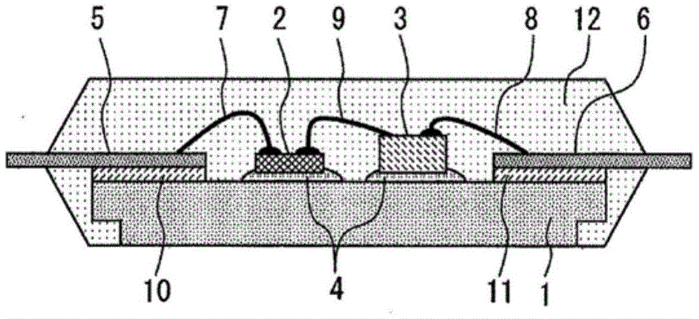
图1是表示本发明的实施方式1涉及的半导体装置的剖面图。图2是表示本发明的实施方式1涉及的半导体装置的内部的俯视图。该半导体装置输出频率大于或等于1GHz、大于或等于1W的电力。FIG. 1 is a cross-sectional view showing a semiconductor device according to
散热器1具有大于或等于200W/cm的导热率,成为GND。在散热器1之上,通过芯片键合材料4而安装有GaN器件或GaAs器件等半导体芯片2、3。使高频信号通过的金属的引线端子5、6分别通过导线7、8而与半导体芯片2、3连接。半导体芯片2、3彼此通过导线9而连接。The
在引线端子5、6的背面分别粘贴具有粘接功能的电介质10、11,经由该电介质10、11而将引线端子5、6粘接于散热器1。电介质10、11彼此分离,分别单独地设置在引线端子5、6与散热器1之间。此外,可以是电介质10、11自身具有粘接功能,也可以在电介质10、11的上下两面设置粘接剂。为了保护半导体芯片2、3不受异物或外力等损害,由环氧树脂构成的封装树脂12将半导体芯片2、3、引线端子5、6以及电介质10、11模塑封装。在封装之后,切去引线端子5、6的一部分,封装件被分离成单独的部件。
这里,在没有电介质10、11的现有技术中,引线端子与散热器之间的材料的介电常数被固定为环氧树脂的大约4.0。另外,如果考虑到框架的加工精度或之后的组装性、导线键合性,则引线端子与散热器之间的距离仅能近至0.25左右。在使高频信号通过的引线端子的宽度为0.5mm的情况下,在现有技术中特性阻抗为约46.5Ω左右。另一方面,在本实施方式中,作为电介质10、11,如果采用例如厚度0.1mmt、介电常数约为3.2的聚酰亚胺材料,则特性阻抗约为29.5Ω左右,能够大幅度变更特性阻抗。Here, in the prior art without the dielectric 10, 11, the dielectric constant of the material between the lead terminal and the heat sink is fixed to about 4.0 of the epoxy resin. In addition, the distance between the lead terminal and the heat sink can only be as short as about 0.25 mm if the processing accuracy of the frame, the subsequent assembly property, and the wire bonding property are taken into consideration. When the width of the lead terminal through which a high-frequency signal passes is 0.5 mm, the characteristic impedance is about 46.5Ω in the prior art. On the other hand, in this embodiment, if a polyimide material with a thickness of 0.1 mmt and a dielectric constant of about 3.2 is used as the
如以上所说明的那样,在本实施方式中,电介质10、11分别单独地设置在引线端子5、6与散热器1之间,彼此分离。因此,能够单独地调整使高频信号通过的引线端子5、6与散热器1的在二维平面上重叠的面积、引线端子5、6与散热器1之间的电介质10、11的介电常数以及厚度。因此,能够将使高频信号通过的引线端子5、6的特性阻抗设定为相对于GaN器件特性来说的最佳值。由此,能够抑制高频特性的损耗。As described above, in the present embodiment, the
实施方式2.
图3是表示本发明的实施方式2涉及的半导体装置的内部的俯视图。在本实施方式中,在使DC偏置通过的引线端子13与散热器1之间单独地设置有电介质14。将具有粘接功能的电介质14粘接至引线端子13的背面,经由该电介质14而将引线端子13粘接至散热器1。引线端子13通过电介质14而被固定至散热器1,通过导线15而与半导体芯片2连接。由此,对于除了使高频信号通过的引线端子5、6以外的端子,也能够改善导线键合性,更牢固地固定引线框和散热器1。其它结构和效果与实施方式1相同。3 is a plan view showing the inside of a semiconductor device according to
实施方式3.
图4是表示本发明的实施方式3涉及的半导体装置的内部的俯视图。电极部16、17分别从使高频信号通过的引线端子5、6的侧面凸出。电极部16、17的形状没有特别限制。由电极部16与散热器1之间的电介质10、电极部16以及散热器1构成电容器。对于电极部17,也同样如此。4 is a plan view showing the inside of a semiconductor device according to
相对于散热器1与电极部16的在二维上重叠的面积S、电介质10的介电常数εr及厚度t,电容器的电容值C由C=εr×S/t求出。通过调整这些参数,从而能够设定电容器的电容值,以使得相对于GaN器件的特性来说是最佳的。The capacitance value C of the capacitor is obtained from the two-dimensionally overlapping area S of the
另外,在高频信号线路上需要开路短截线等电容器的情况下,能够通过本构造而对引线端子附加该功能。其结果,能够最大限度地发挥GaN器件的特性。另外,由于将引线框的一部分作为电容器,因此不需要追加的部件成本,实现器件的成本降低。In addition, when a capacitor such as an open stub is required on a high-frequency signal line, this structure can add this function to the lead terminal. As a result, the characteristics of the GaN device can be brought into full play. In addition, since a part of the lead frame is used as a capacitor, additional component cost is not required, and the cost of the device can be reduced.
实施方式4.
图5是表示本发明的实施方式4涉及的半导体装置的剖面图。图6是沿着图5的I-II的剖面图。封装树脂12的上表面成型为凹型形状。此外,也可以将封装树脂12的上表面成型为凸型形状。在包含该凹部的封装树脂12的表面整面形成有金属膜18。金属膜18与引线端子或成为GND的散热器1连接。由此,使高频信号通过的引线端子5、6成为上下由GND屏蔽包围的带状线的构造。因此,从引线端子5、6泄漏的电磁波变少,并且变得不易受到来自外部的电磁波的影响,因此能够使GaN器件的特性稳定化。另外,通过调整配置在引线端子5、6之上的封装树脂12的厚度而使引线端子5、6与金属膜18之间的距离最佳化,从而能够增加特性阻抗的设计自由度。5 is a cross-sectional view showing a semiconductor device according to
实施方式5.
图7是表示本发明的实施方式5涉及的半导体装置的剖面图。图8是将本发明的实施方式5涉及的引线端子放大后的俯视图。图9是将本发明的实施方式5涉及的引线端子放大后的仰视图。引线端子19、20不是一块金属体,而是上表面金属21、电介质22以及下表面金属23、24的3层构造。7 is a cross-sectional view showing a semiconductor device according to
上表面金属21形成在电介质22的上表面。下表面金属23在封装树脂12的内部形成于电介质22的下表面,通过导电性粘接剂等而直接粘接于散热器1。下表面金属24在封装树脂12的外部形成于电介质22的下表面。通路孔25在封装树脂12的外部的引线端子19、20的端部附近,贯穿电介质22而将上表面金属21和下表面金属24连接。下表面金属23和下表面金属24在封装树脂12的内部与外部的边界处以彼此电绝缘的方式分开。The
在本实施方式中,能够通过引线端子19、20的结构设计而使特性阻抗最佳化。但是,如果高频信号在引线端子19、20的上表面传送,则即使将封装件安装于2次安装基板,也无法容易地连接信号。因此,通过通路孔25而将上表面金属21与下表面金属24连接,将信号传送到引线端子19、20的下表面。下表面金属24是与2次安装的基板接合的电极焊盘。In the present embodiment, the characteristic impedance can be optimized by structural design of the
另外,在实施方式1~4中,散热器1与引线端子19、20重叠的部分能够设定为最佳的阻抗。但是,在从散热器1的端部到2次安装基板端部之间,在引线端子19、20之下不存在散热器1,因此,尽管距离短,但特性阻抗产生偏差。与此相对,在本实施方式中,下表面金属23延伸到与散热器1的端部相比更外侧。因此,在从散热器1的端部到2次安装基板的端部之间,在引线端子19、20的下表面也存在成为GND的下表面金属23,因此,没有特性品阻抗的偏差,能够抑制高频特性的损耗。In addition, in
标号的说明Explanation of labels
1散热器,2、3半导体芯片,5、6、13、19、20引线端子,10、11、14电介质,12封装树脂,16、17电极部,18金属膜,21上表面金属,23、24下表面金属,25通路孔。1 radiator, 2, 3 semiconductor chip, 5, 6, 13, 19, 20 lead terminal, 10, 11, 14 dielectric, 12 packaging resin, 16, 17 electrode part, 18 metal film, 21 upper surface metal, 23, 24 lower surface metal, 25 via holes.
Claims (6)
Applications Claiming Priority (1)
| Application Number | Priority Date | Filing Date | Title |
|---|---|---|---|
| PCT/JP2017/019793 WO2018216219A1 (en) | 2017-05-26 | 2017-05-26 | Semiconductor device |
Publications (2)
| Publication Number | Publication Date |
|---|---|
| CN110663109A CN110663109A (en) | 2020-01-07 |
| CN110663109B true CN110663109B (en) | 2023-06-13 |
Family
ID=62106159
Family Applications (1)
| Application Number | Title | Priority Date | Filing Date |
|---|---|---|---|
| CN201780091077.6A Active CN110663109B (en) | 2017-05-26 | 2017-05-26 | Semiconductor device with a semiconductor device having a plurality of semiconductor chips |
Country Status (4)
| Country | Link |
|---|---|
| US (1) | US10923444B1 (en) |
| JP (1) | JP6319525B1 (en) |
| CN (1) | CN110663109B (en) |
| WO (1) | WO2018216219A1 (en) |
Families Citing this family (4)
| Publication number | Priority date | Publication date | Assignee | Title |
|---|---|---|---|---|
| JP2020188082A (en) * | 2019-05-13 | 2020-11-19 | 合同会社オフィス西村 | Semiconductor package |
| JP7193008B2 (en) * | 2019-10-15 | 2022-12-20 | 三菱電機株式会社 | semiconductor equipment |
| CN111933595A (en) * | 2020-07-16 | 2020-11-13 | 杰群电子科技(东莞)有限公司 | Semiconductor packaging structure and manufacturing method thereof |
| DE102022213479A1 (en) | 2022-12-12 | 2024-06-13 | Robert Bosch Gesellschaft mit beschränkter Haftung | Power module with a molded body and molded lip |
Family Cites Families (17)
| Publication number | Priority date | Publication date | Assignee | Title |
|---|---|---|---|---|
| JPS629652A (en) * | 1985-07-05 | 1987-01-17 | Mitsubishi Electric Corp | Semiconductor device |
| JPS63124759U (en) * | 1987-02-09 | 1988-08-15 | ||
| JPH0199247A (en) * | 1987-10-13 | 1989-04-18 | Mitsubishi Electric Corp | Lead frame |
| JPH0195756U (en) * | 1987-12-16 | 1989-06-26 | ||
| JP2742610B2 (en) | 1989-11-27 | 1998-04-22 | 京セラ株式会社 | Package for storing semiconductor elements |
| JP2797557B2 (en) * | 1989-11-28 | 1998-09-17 | 日本電気株式会社 | Integrated circuit device having shield function and manufacturing method |
| JPH04278570A (en) * | 1991-03-07 | 1992-10-05 | Nec Corp | IC lead frame |
| JPH0661363A (en) * | 1992-02-12 | 1994-03-04 | Fujitsu Ltd | Semiconductor device, manufacturing method thereof, semiconductor manufacturing device, carrier and test jig |
| JPH0631157U (en) * | 1992-09-28 | 1994-04-22 | 日本電気株式会社 | LSI lead frame |
| JPH06244337A (en) * | 1993-02-18 | 1994-09-02 | Dainippon Printing Co Ltd | Lead frame for mounting electronic circuit element and electronic circuit using the same |
| JPH0778930A (en) * | 1993-07-15 | 1995-03-20 | Nec Corp | Semiconductor device and its external leads |
| JP2596399B2 (en) * | 1995-03-30 | 1997-04-02 | 日本電気株式会社 | Semiconductor device |
| TW526600B (en) * | 2002-02-08 | 2003-04-01 | United Test Ct Inc | Semiconductor device including a heat spreader |
| JP3803596B2 (en) * | 2002-03-14 | 2006-08-02 | 日本電気株式会社 | Package type semiconductor device |
| JP2004200264A (en) * | 2002-12-17 | 2004-07-15 | Renesas Technology Corp | Semiconductor device and method of manufacturing the same |
| JP4509052B2 (en) * | 2005-03-29 | 2010-07-21 | 三洋電機株式会社 | Circuit equipment |
| US8937374B2 (en) | 2011-12-22 | 2015-01-20 | Panasonic Corporation | Semiconductor package, method and mold for producing same, input and output terminals of semiconductor package |
-
2017
- 2017-05-26 JP JP2017550957A patent/JP6319525B1/en active Active
- 2017-05-26 CN CN201780091077.6A patent/CN110663109B/en active Active
- 2017-05-26 US US16/490,481 patent/US10923444B1/en active Active
- 2017-05-26 WO PCT/JP2017/019793 patent/WO2018216219A1/en not_active Ceased
Also Published As
| Publication number | Publication date |
|---|---|
| JP6319525B1 (en) | 2018-05-09 |
| CN110663109A (en) | 2020-01-07 |
| JPWO2018216219A1 (en) | 2019-06-27 |
| US10923444B1 (en) | 2021-02-16 |
| WO2018216219A1 (en) | 2018-11-29 |
Similar Documents
| Publication | Publication Date | Title |
|---|---|---|
| US12027465B2 (en) | Impedance controlled electrical interconnection employing meta-materials | |
| CN207399201U (en) | transceiver module | |
| US20060276157A1 (en) | Apparatus and methods for packaging antennas with integrated circuit chips for millimeter wave applications | |
| CN103094238B (en) | Lead frame and semiconductor devices | |
| JPS6325710B2 (en) | ||
| CN110663109B (en) | Semiconductor device with a semiconductor device having a plurality of semiconductor chips | |
| CN111937138B (en) | Semiconductor devices | |
| CN103367268A (en) | PCB based RF-power package window frame | |
| WO2013094101A1 (en) | Semiconductor package, method and mold for producing same, input and output terminals of semiconductor package | |
| TWI594380B (en) | Package structure and three-dimensional package structure | |
| JPH0629428A (en) | Semiconductor device | |
| US9041169B2 (en) | Semiconductor packaging container, semiconductor device, electronic device | |
| JP5412372B2 (en) | Semiconductor mounting equipment | |
| JP7666175B2 (en) | Semiconductor device and package | |
| CN113169128B (en) | Semiconductor device and antenna device | |
| EP2500938A1 (en) | Package for a semiconductor device, and a method of manufacturing such package | |
| US20110186979A1 (en) | Semiconductor package and high-frequency semiconductor device | |
| US20250125286A1 (en) | Semiconductor device | |
| US9324649B2 (en) | Semiconductor device including a cap substrate on a side wall that is disposed on a semiconductor substrate | |
| CN101515579A (en) | Semiconductor device and electronic apparatus | |
| Evans et al. | Electrical, Thermal, Reliability and Cost Considerations for Millimeter-Wave Surface Mount Packages |
Legal Events
| Date | Code | Title | Description |
|---|---|---|---|
| PB01 | Publication | ||
| PB01 | Publication | ||
| SE01 | Entry into force of request for substantive examination | ||
| SE01 | Entry into force of request for substantive examination | ||
| GR01 | Patent grant | ||
| GR01 | Patent grant |