Disclosure of Invention
Embodiments of the present invention provide a display panel, a method for manufacturing the same, and a display device, which can disconnect a light emitting functional layer in an isolation region, and prevent water vapor and oxygen from entering a pixel region from an opening of an opening region.
In order to achieve the above purpose, the embodiment of the invention adopts the following technical scheme:
in one aspect, a display panel is provided, which has a display region including a pixel region, an opening region, and an isolation region located between the pixel region and the opening region, wherein the isolation region is disposed around the opening region.
The pixel region is provided with a light emitting function layer on a substrate.
At least one isolation column which is positioned on the same side of the substrate and the light-emitting functional layer is arranged in the isolation region, the isolation column is arranged around the opening region in a circle, and the longitudinal section of the isolation column is I-shaped; and a first groove is arranged around the isolation column at one side of the isolation column close to the lower surface of the substrate.
And the light-emitting functional layer extends to the part of the isolation region and is disconnected at the side surface of the isolation column.
Optionally, the display panel further includes a protection pattern disposed on a side of the isolation pillar away from the substrate; the orthographic projection of the protection pattern on the substrate covers the orthographic projection of the isolation column on the substrate.
Optionally, the thickness of the protective pattern is 10nm to 100 nm.
Optionally, in the thickness direction of the substrate, the isolation pillar includes a first isolation portion, a second isolation portion, and a third isolation portion that are sequentially stacked, and each side surface of the second isolation portion retracts inward relative to the first isolation portion and the third isolation portion.
The materials of the first isolation part and the third isolation part are the same, the material of the second isolation part is different from that of the first isolation part and that of the third isolation part, and the etching rate of the material of the second isolation part is greater than that of the material of the first isolation part and that of the third isolation part.
Optionally, a driving circuit is further disposed in the pixel region between the substrate and the light-emitting functional layer, and the driving circuit includes a thin film transistor, where the thin film transistor includes a gate, a source, and a drain.
At least one of the first, second and third isolation portions is of the same material as the gate or the source and drain.
Optionally, the thin film transistor further includes an active layer and a gate insulating layer; the active layer, the gate insulating layer, the gate electrode, the source electrode and the drain electrode are sequentially arranged along a direction far away from the substrate; the source electrode and the drain electrode are in contact with the active layer through a via hole in the interlayer insulating layer.
The isolation column is arranged on the surface of the interlayer insulating layer, and the first groove is located on the interlayer insulating layer.
The isolation column is made of the same material as the source electrode and the drain electrode.
Optionally, the display device further includes a flat layer pattern, and the flat layer pattern is disposed between the driving circuit and the light emitting functional layer and covers the pixel region.
The flat layer pattern and the protection pattern are made of the same material.
And the thickness of the flat layer pattern is greater than that of the protective pattern.
Optionally, the number of the isolation columns is two, and the two isolation columns are arranged at intervals.
Optionally, a first retaining wall and a second retaining wall are further arranged in the isolation region, and the first retaining wall and the second retaining wall are arranged around the open region for a circle; the first retaining wall is arranged between the isolation column and the second retaining wall.
And the lower surface of the second retaining wall is provided with a raised part.
The first retaining wall, the second retaining wall and the pixel define the same layer and the same material of the structure, wherein the pixel defines the structure and is used for isolating adjacent light-emitting devices, and each light-emitting device comprises the light-emitting functional layer, an anode and a cathode, wherein the light-emitting functional layer is close to one side of the substrate, and the cathode is far away from one side of the substrate.
Optionally, the pad-up portion and the flat layer pattern are made of the same material.
Optionally, a second groove is further disposed on one side of the raised portion close to the lower surface of the substrate, and the periphery of the raised portion close to the opening region.
Optionally, the depth range of the first groove and the second groove is 500nm to 1500 nm.
Optionally, the substrate is a flexible substrate.
In another aspect, a display device is provided, which includes the display panel described above.
In another aspect, a method for manufacturing a display panel having a display region including a pixel region, an open region, and an isolation region located between the pixel region and the open region is provided.
The preparation method of the display panel comprises the following steps:
and forming at least one isolation column transition structure on the substrate and in the isolation region by a dry etching process, wherein the isolation column transition structure surrounds the opening region for a circle.
And forming a protection pattern on the upper surface of the isolation column transition structure far away from the substrate.
And carrying out a wet etching process on the isolation column transition structure to form an isolation column, wherein the longitudinal section of the isolation column is I-shaped.
And forming a light-emitting functional layer positioned in the pixel region and the isolation region on the substrate on which the isolation column is formed, wherein the light-emitting functional layer is positioned in the isolation region and is disconnected on the side surface of the isolation column.
Optionally, before forming the pillar transition structure, the method for manufacturing a display panel further includes:
and forming a first groove around the to-be-formed isolation column transition structure, wherein the first groove is recessed towards one side of the substrate relative to one side of the isolation column transition structure, which is close to the lower surface of the substrate.
Optionally, forming at least one isolation pillar transition structure on the substrate and in the isolation region by a dry etching process, including:
sequentially forming a first isolation film, a second isolation film and a third isolation film on the substrate, wherein the first isolation film, the second isolation film and the third isolation film cover the isolation region and are stacked; the first isolation film and the third isolation film are made of the same material, the second isolation film is made of a different material from the first isolation film and the third isolation film, and the etching rates of the first isolation film and the third isolation film are greater than the etching rate of the second isolation film.
And etching the first isolation film, the second isolation film and the third isolation film by a dry etching process to form at least one isolation column transition structure, wherein the isolation column transition structure comprises a first isolation pattern, a second isolation pattern and a third isolation pattern.
Optionally, the method further includes forming a driving circuit between the substrate and the light-emitting functional layer in the pixel region, where the driving circuit includes a thin film transistor.
The thin film transistor includes a gate electrode, a source electrode, and a drain electrode.
At least one of the first isolation pattern, the second isolation pattern, and the third isolation pattern is formed in synchronization with the gate electrode or the source and drain electrodes.
Optionally, forming the thin film transistor and the isolation pillar transition structure includes:
an active layer, a gate insulating layer and a gate electrode are sequentially formed on a substrate.
And forming an interlayer insulating layer, wherein the interlayer insulating layer comprises a first via hole and a second via hole, and the first via hole and the second via hole are respectively exposed out of the parts of the active layer positioned at two sides of the grid electrode.
And sequentially forming the first isolation film, the second isolation film and the third isolation film on the interlayer insulating layer, wherein the first isolation film, the second isolation film and the third isolation film cover the pixel region and the isolation region.
Performing dry etching on the first isolation film, the second isolation film and the third isolation film, and forming a source electrode and a drain electrode in the pixel region, wherein the source electrode and the drain electrode are both of a three-layer structure and are in contact with the active layer through the first via hole and the second via hole respectively; and simultaneously, forming the isolation column transition structure in the isolation region.
Optionally, after the driving circuit is formed and before the light emitting functional layer is formed, the method for manufacturing a display panel further includes:
and forming a flat layer film covering the pixel region and the isolation region.
And etching the flat layer film by using a half-tone mask to form a flat layer pattern covering the pixel area and simultaneously form the protection pattern.
Wherein a thickness of the planarization layer pattern is greater than a thickness of the protection pattern.
Optionally, the step-up portion located in the isolation region is also formed simultaneously with the formation of the planarization layer pattern.
After the forming the planarization layer pattern, the protection pattern, and the raised portion, and before the forming the light emitting functional layer, the method of manufacturing a display panel further includes:
and forming an anode in the pixel region.
Forming a pixel defining structure on the substrate on which the anode is formed, and synchronously forming a first retaining wall and a second retaining wall on the isolation region, wherein the first retaining wall and the second retaining wall surround the opening region for a circle; the first retaining wall is located between the isolation column and the second retaining wall, and the second retaining wall is formed above the heightening part.
After the forming of the light emitting functional layer, the method of manufacturing a display panel further includes: a cathode is formed.
Wherein the anode, the light emitting function layer, and the cathode positioned at each sub-pixel region in the pixel region constitute a light emitting device.
On the other hand, the invention also provides a display panel, which is obtained by the preparation method of the display panel.
The embodiment of the invention provides a display panel, a preparation method thereof and a display device, wherein a display area of the display panel is provided with a pixel area, an opening area and an isolation area, at least one isolation column is arranged in the isolation area, the isolation column is arranged around the opening area for a circle, and the longitudinal section of the isolation column is I-shaped; a first groove is formed around the isolation column on one side of the lower surface, close to the substrate, of the isolation column. In order to prevent the moisture and the oxygen from spreading from the opening region to the light-emitting functional layer in the pixel region, an isolation region is disposed between the opening region and the pixel region, and the isolation column and the first groove are disposed in the isolation region. On one hand, the longitudinal section of the isolation column is I-shaped, and the film layer is disconnected on the side surface of the isolation column due to the I-shaped structure when the light-emitting functional layer is subjected to vapor deposition. After the light-emitting functional layer is isolated, water vapor and oxygen entering from the open hole region can only spread to the light-emitting functional layer in the isolation region along the light-emitting functional layer extending to the open hole region and cannot continue to extend to the light-emitting functional layer in the pixel region, so that the isolation column plays a role in isolating the water vapor and the oxygen. On the other hand, the height of the isolation column is increased to a certain extent due to the arrangement of the first groove, and the section difference of the disconnection of the light-emitting functional layer is increased when the light-emitting functional layer is evaporated, so that the disconnection of the light-emitting functional layer on the side face of the isolation column is easier.
Detailed Description
The technical solutions in the embodiments of the present invention will be clearly and completely described below with reference to the drawings in the embodiments of the present invention, and it is obvious that the described embodiments are only a part of the embodiments of the present invention, and not all of the embodiments. All other embodiments, which can be derived by a person skilled in the art from the embodiments given herein without making any creative effort, shall fall within the protection scope of the present invention.
The full-screen is a display screen with an ultrahigh screen occupation ratio, and the ideal full-screen display occupation ratio is 100%, namely, the front of the mobile phone is a display interface. The mobile phone screen is limited by the installation requirements of indispensable basic functional components of mobile phones such as a front camera of the mobile phone, a mobile phone receiver, a face recognition sensor and a light sensor, and at present, a certain gap is required to be reserved above the mobile phone screen to install the functional components, so that display screens such as a bang screen and a water drop screen are formed.
Based on this, as shown in fig. 1, fig. 2a, fig. 2b and fig. 2c, the embodiment of the invention provides a display panel 1 having a display region 10, the display region 10 includes a pixel region 101, an opening region 102, and an isolation region 103 located between the pixel region 101 and the opening region 102, and the isolation region 103 is disposed around the opening region 102.
The pixel region 101 is provided with a light-emitting function layer 1014 on the substrate 13.
At least one isolation post 1031 which is positioned on the same side of the substrate 13 as the light-emitting functional layer 1014 is arranged in the isolation region 103, the isolation post 1031 is arranged around the open hole region 102 in a circle, and the longitudinal section of the isolation post 1031 is in an i shape; a first groove 151 is provided around the isolation post 1031 on the side of the isolation post 1031 near the lower surface of the substrate 13.
The light emitting function layer 1014 extends to the isolation region 103, and is disconnected at the side of the isolation post 1031.
In addition, as shown in fig. 1, a peripheral region 11 is further provided at the periphery of the display region 10, and the peripheral region 11 is used for wiring. It should be noted that, in fig. 1, the peripheral area 11 is disposed around the display area 10 by one circle, but the embodiment of the invention is not limited thereto, and the peripheral area 11 may also be disposed not by one circle, for example, disposed on two opposite sides of the display area 10.
The pixel region 101 in the display region 10 is used for displaying a picture, and the pixel region 101 includes a plurality of sub-pixels including at least a first color sub-pixel, a second color sub-pixel, and a third color sub-pixel. Illustratively, the first color sub-pixel, the second color sub-pixel, and the third color sub-pixel are a red sub-pixel, a green sub-pixel, and a blue sub-pixel, respectively. For the first color sub-pixel, the second color sub-pixel and the third color sub-pixel, the distribution thereof may refer to the conventional arrangement in the art.
Each subpixel includes, in addition to the above-described light-emitting functional layer 1014, an anode 1012 provided on the side of the light-emitting functional layer 1014 close to the substrate 13, and a cathode 1013 provided on the side remote from the substrate 13. Here, in each sub-pixel, the anode 1012, the light-emitting function layer 1014, and the cathode 1013 constitute one light-emitting device 1011.
Here, the light-emitting function layer 1014 includes at least a light-emitting layer. As shown in fig. 3, the light-emitting function layer 1014 may further include an Electron Transport Layer (ETL) 1016, an Electron Injection Layer (EIL) 1017, a Hole Transport Layer (HTL) 1018, and a Hole Injection Layer (HIL) 1019, in addition to the light-emitting layer 1015. Of course, the light-emitting function layer 1014 may include portions of ETL1016, EIL1017, HTL1018, and HIL1019 in addition to the light-emitting layer 1015.
The opening region 102 is used for assembling a camera or the like after the opening process, and the shape of the opening region 102 may be, for example, a circular shape as shown in fig. 1, or may be other regular shapes such as a rectangular shape. In the display panel 1 of the present invention, as shown in fig. 2a and 2c, the opening process may not be performed in the opening region 102, and in this case, the opening process may be performed before the camera is assembled. In addition, as shown in fig. 2b, the display panel 1 of the present invention may also have an opening process performed in the opening region 102, in which case the display panel 1 can be directly taken for subsequent assembly.
At least one isolation post 1031 is disposed in the isolation region 103, and the isolation post 1031 is disposed around the opening region 102. For example, in the case that the shape of the opening region 102 is a circle, the top view of the isolation post 1031 may also be a circular ring. In the case where the shape of the opening region 102 is rectangular, the top view of the isolation post 1031 may also be rectangular.
When the number of the isolation pillars 1031 is two or more, a plurality of isolation pillars 1031 are arranged at intervals.
The separator 1031 is i-shaped in longitudinal section. That is, as shown in fig. 4a, the isolation post 1031 includes a first isolation portion 1032, a second isolation portion 1033, and a third isolation portion 1034 that are sequentially stacked, and each side surface of the second isolation portion 1033 is inwardly recessed with respect to the first isolation portion 1032 and the third isolation portion 1034 in the thickness direction of the substrate 13.
Wherein, widths of the first isolation portion 1032 and the third isolation portion 1034 of the isolation pillar 1031 may be equal, for example, and a width of the second isolation portion 1033 is smaller than those of the first isolation portion 1032 and the third isolation portion 1034. Since the width of the second isolation 1033 is smaller than the widths of the first and third isolation 1032 and 1034, the fabricated light emitting function layer 1014 may be disconnected at the side of the isolation post 1031.
On this basis, the first groove 151 is provided around the isolation post 1031, and the first groove 151 may increase the probability that the light emission function layer 1014 is broken at the side of the isolation post 1031.
Wherein the first grooves 151 are arranged around the isolation post 1031 in a circle, the first grooves 151 are not limited to one, and when the number of the first grooves 151 is plural, the plural first grooves 151 are arranged at intervals.
The first recess 151 may be located at a surface of an insulating layer located at one side of the substrate 13, and the isolation post 1031 is located at the surface of the insulating layer.
The embodiment of the invention provides a display panel 1, a display area 10 of the display panel 1 has a pixel area 101, an open area 102 and an isolation area 103, at least one isolation column 1031 is arranged in the isolation area 103, the isolation column 1031 is arranged around the open area 102 for one circle, and a longitudinal section of the isolation column 1031 is in an i shape; a first groove 151 is provided around the isolation post 1031 on the side of the isolation post 1031 near the lower surface of the substrate 13. Since external moisture and oxygen enter the display panel 1 from the opening region 102 and the light-emitting functional layer 1014 in the pixel region 101 also extends into the opening region 102, in order to prevent moisture and oxygen from spreading from the opening region 102 to the light-emitting functional layer 1014 in the pixel region 101, the isolation region 103 is provided between the opening region 102 and the pixel region 101, and the isolation pillar 1031 and the first groove 151 are provided in the isolation region 103. On one hand, the isolation post 1031 has an i-shaped longitudinal section, and when the light emitting functional layer 1014 is subjected to vapor deposition, the film layer is broken at the side surface of the isolation post 1031 due to the i-shaped structure. After the light-emitting functional layer 1014 is isolated, water vapor and oxygen entering from the opening region 102 can only spread to the light-emitting functional layer 1014 located in the isolation region 103 along the light-emitting functional layer 1014 extending to the opening region 102, and cannot continue to extend to the light-emitting functional layer 1014 located in the pixel region 101, so that the isolation column 1031 plays a role in isolating water vapor and oxygen. On the other hand, the first grooves 151 increase the height of the isolation pillars 1031 to some extent, and increase the step difference of the light-emitting function layer 1014 during the evaporation of the light-emitting function layer 1014, so that the light-emitting function layer 1014 is more easily broken at the side surfaces of the isolation pillars 1031.
Optionally, as shown in fig. 2c, fig. 4a and fig. 4b, the display panel 1 further includes a protection pattern 1035 disposed on a side of the isolation post 1031 away from the substrate 13; an orthographic projection of protective pattern 1035 on substrate 13 covers an orthographic projection of isolation post 1031 on substrate 13.
It is understood that the protection pattern 1035 is disposed on a side of the third isolation section 1034 away from the substrate 13, i.e., the protection pattern 1035 does not contact with a side surface of the isolation pillar 1031. As shown in fig. 2c and fig. 4a, the protection pattern 1035 may completely coincide with an orthographic projection of the third isolation portion 1034 on the substrate 13, or, as shown in fig. 4b, the protection pattern 1035 is raised above an edge of the upper surface of the third isolation portion 1034 with respect to the third isolation portion 1034.
The protective pattern 1035 may be provided, in one aspect, by forming the protective pattern 1035 and then etching the film layer thereunder, thereby forming the isolation post 1031. In this case, the protective pattern 1035 may protect the third isolation section 1034 of the isolation pillar 1031, so as to prevent the length of the third isolation section 1034 from being smaller than the preset value due to the excessively fast etching speed of the etching solution; on the other hand, as shown in fig. 4b, even if the length of the third isolating portion 1034 is smaller than the predetermined value due to the influence of the etching solution, since the protective pattern 1035 is not influenced by the etching solution and is formed and cured first, the length of the protective pattern 1035 does not change before and after etching, and thus the isolation posts 1031 and the protective pattern 1035 are still in an i shape as a whole, and the light emitting function layer 1014 is still disconnected.
Optionally, the thickness of the protective pattern 1035 is 10nm to 100 nm.
The thickness of the protective pattern 1035 is set within the above range, so that the overall thickness of the isolation pillar 1031 and the protective pattern 1035 is prevented from being too large, thereby affecting the subsequent process.
Optionally, the materials of the first isolation portion 1032 and the third isolation portion 1034 are the same, the material of the second isolation portion 1033 is different from the materials of the first isolation portion 1032 and the third isolation portion 1034, and the etching rate of the material of the second isolation portion 1033 is greater than the etching rate of the materials of the first isolation portion 1032 and the third isolation portion 1034. It is understood that the etching rate of the material of the second isolation portions 1033 is greater than that of the materials of the first isolation portions 1032 and the third isolation portions 1034, if the same etching solution is used.
By providing the first isolation portion 1032 and the third isolation portion 1034 with the same material, and the second isolation portion 1033 with a material different from that of the first isolation portion 1032 and the third isolation portion 1034, the isolation pillar 1031 may be formed into a structure with an "i" shaped longitudinal section through an etching process.
Illustratively, each side of the second isolation portion 1033 is inwardly recessed by 1 μm to 2 μm with respect to the first isolation portion 1032 and the third isolation portion 1034. Alternatively, the side surfaces of the second partition 1033 are recessed with respect to the first partition 1032 and the third partition 1034 by an amount equal to the thickness of the light emitting function layer 1014.
Since different materials have different etching rates in the same etching solution, by setting the materials of the first isolation portion 1032 and the third isolation portion 1034 to be the same, the material of the second isolation portion 1033 is different from the material of the first isolation portion 1032 and the third isolation portion 1034, and the etching rate of the material of the second isolation portion 1033 is greater than the etching rate of the material of the first isolation portion 1032 and the third isolation portion 1034, so that the required retraction amount can be formed by using the etching solution and controlling the etching time when the isolation pillars 1031 are manufactured.
For example, the material of the first and third isolation portions 1032 and 1034 may be Ti (titanium), and the material of the second isolation portion 1033 may be Al (aluminum).
Optionally, in the pixel region 101, a driving circuit 12 is further disposed between the substrate 13 and the light emitting function layer 1014, and the driving circuit 12 includes a Thin-film transistor (TFT). The thin film transistor 14, as shown by a dotted frame in fig. 2a, 2b and 2c, includes a gate electrode 141, a source electrode 142 and a drain electrode 143. It should be noted that the driving circuit 12 may include a capacitor in addition to the thin film transistor 14, but fig. 2a, 2b, and 2c only illustrate that the driving circuit 12 includes the thin film transistor 14.
At least one of the first, second, and third isolation portions 1032, 1033, 1034 is of the same material as the gate 141 or the source and drain electrodes 142, 143.
The driving circuit 12 is used to drive the light emitting device 1011 to emit light. When the driving circuit 12 is fabricated, the portion of the driving circuit 12 extending into the isolation region 103 can be directly used to form the isolation post 1031, which facilitates fabrication of the isolation post 1031.
In the case where the first isolation portion 1032 is of the same material as the gate 141 or the source and drain electrodes 142 and 143, optionally, the thickness of the first isolation portion 1032 is greater than the thickness of the third isolation portion 1034. Since the thickness of the gate electrode 141 or the source and drain electrodes 142 and 143 has some influence on the circuit in the thin film transistor 14, the thickness needs to be ensured, and thus, the thickness of the first isolation portion 1032 may be larger than that of the third isolation portion 1034.
Alternatively, as shown in fig. 2a, 2b and 2c, the thin film transistor 14 further includes an active layer 144 and a gate insulating layer 145; the active layer 144, the gate insulating layer 145, the gate electrode 141, the source electrode 142, and the drain electrode 143 are sequentially disposed in a direction away from the substrate 13; the source and drain electrodes 142 and 143 contact the active layer 144 through vias 153 on the interlayer insulating layer 15. That is, the thin film transistor 14 is a top gate thin film transistor.
On this basis, the isolation pillar 1031 is disposed on the surface of the interlayer insulating layer 15, and the first groove 151 is located on the interlayer insulating layer 15, that is, the first groove 151 is formed by partially etching the interlayer insulating layer 15. Meanwhile, the isolation pillar 1031 is of the same material as the source and drain electrodes 142 and 143.
For example, in the case where the material of the first and third isolation portions 1032 and 1034 in the isolation pillar 1031 is Ti (titanium) and the second isolation portion 1033 is Al (aluminum), the source and drain electrodes 142 and 143 also include a three-layer structure in which the middle layer is Al and the other two layers are Ti.
The material of the interlayer insulating layer 15 may be any of polybenzobisoxazole, photosensitive polyimide, benzocyclobutene, and inorganic materials, for example.
The first groove 151 is provided on the interlayer insulating layer 15, and the first groove 151 increases a step when the light emitting function layer 1014 rises along the side surface of the isolation post 1031, so that the light emitting function layer 1014 is more easily disconnected at the side surface of the isolation post 1031.
Optionally, as shown in fig. 2a, fig. 2b and fig. 2c, the display panel 1 further includes a flat layer pattern 160, and the flat layer pattern 160 is disposed between the driving circuit 12 and the light emitting functional layer 1014 and covers the pixel region 101. The flat layer pattern 160 and the protective pattern 1035 are of the same material, and the thickness of the flat layer pattern 160 is greater than the thickness of the protective pattern 1035.
The planarization layer pattern 160 serves to planarize the surfaces of the source electrode 142 and the drain electrode 143 in the thin film transistor 14, facilitating the subsequent fabrication of the light emitting function layer 1014. The material of the planarization layer 16 may be, for example, photosensitive polyimide.
On one hand, the flat layer pattern 160 and the protective pattern 1035 are made of the same material in the same layer, that is, the flat layer pattern 160 and the protective pattern 1035 are formed simultaneously, so that the manufacturing process can be simplified; on the other hand, by making the thickness of the protective pattern 1035 smaller than that of the planarization pattern 160, it is possible to facilitate subsequent production of the light-emitting functional layer 1014 and other film layers on the upper side of the light-emitting functional layer 1014.
Optionally, as shown in fig. 5, the number of the isolation pillars 1031 is two, and the two isolation pillars 1031 are arranged at intervals.
The two isolation pillars 1031 may increase the probability that the light emission function layer 1014 is disconnected at the sides of the isolation pillars 1031.
In addition, as shown in fig. 2a, 2b and 2c, the display panel 1 further includes a first inorganic encapsulation layer 19, an organic layer 20 and a second inorganic encapsulation layer 21, which are sequentially stacked.
The first inorganic encapsulating layer 19 and the second inorganic encapsulating layer 21 serve to prevent moisture and oxygen entering from the front surface of the display panel 1 from entering the light emitting functional layer 1014. The material of the first inorganic encapsulating layer 19 and the second inorganic encapsulating layer 21 is an inorganic substance such as silicon nitride and/or silicon oxide. The organic layer 20 is used to prevent the inorganic particles in the first inorganic encapsulation layer 19 from affecting the preparation of the second inorganic encapsulation layer 21, and thus the film of the second inorganic encapsulation layer 21 is broken, so that the organic layer 20 is required to be disposed to planarize the first inorganic encapsulation layer 19, and the material of the organic layer 20 may be acrylic, for example.
Optionally, as shown in fig. 2a, fig. 2b and fig. 2c, a first retaining wall 1036 and a second retaining wall 1037 are further disposed in the isolation region 103, and the first retaining wall 1036 and the second retaining wall 1037 are disposed around the open region 102; the first retaining wall 1036 is disposed between the isolation column 1031 and the second retaining wall 1037; the raised portion 161 is disposed on the lower surface of the second wall 1037 opposite to the first wall 1036. The first retaining wall 1036, the second retaining wall 1037 and the pixel defining structure 18 are made of the same material at the same layer, wherein the pixel defining structure 18 is used to isolate the adjacent light emitting devices 1011, as shown in fig. 6.
Since the material of the organic layer 20 has a certain fluidity, in order to facilitate the preparation of the organic layer 20, the first retaining wall 1036 is provided to intercept the flow of the material of the organic layer 20 toward the side near the open region 102. The second wall 1037 is used to further intercept the material of the organic layer 20, so as to avoid the material of the organic layer 20 from spreading toward the opening region 102 due to insufficient interception capability of the first wall 1036. The longitudinal sectional shapes of the first retaining wall 1036 and the second retaining wall 1037 may be, for example, a trapezoid, a rectangle, or the like. In the case where the longitudinal sectional shapes of the first retaining wall 1036 and the second retaining wall 1037 are trapezoidal, the length of the top side of the trapezoid is smaller than the length of the bottom side thereof.
The pixel defining structure 18 is disposed on a side of the flat layer pattern 160 away from the substrate 13 in the pixel region 101, and the pixel defining structure 18 is used to separate the adjacent light emitting devices 1011 to avoid the occurrence of crosstalk. Wherein the pixel defining structure 18 may cover a portion of the anode 1012, i.e., the anode 1012 is formed first and the pixel defining structure 18 is formed after the anode 1012.
The pixel defining structure 18 can be made of, for example, a photoresist, and the photoresist includes one or more of polyimide, organosilane, and polymethylmethacrylate.
Alternatively, as shown in fig. 2a, 2b and 2c, the raised portion 161 and the planarization layer pattern 160 are made of the same material in the same layer.
The height of the raised portion 161 may be 1.5 μm, for example. The raised portion 161 serves to increase the ability of the second barrier 1037 to intercept the material of the organic layer 20. In addition, the material of the raised portion 161 and the material of the flat layer pattern 160 are the same, and the raised portion 161 and the flat layer pattern 160 are formed simultaneously, so that the manufacturing process can be simplified.
Optionally, as shown in fig. 2a, 2b and 2c, a second groove 152 is further disposed on a side of the raised portion 161 close to the lower surface of the substrate 13, and a periphery of the raised portion 161 close to the opening region 102.
The second recess 152 is disposed in the same manner as the first recess 151, that is, the second recess 152 is also disposed on the interlayer insulating layer 15, and the second recess 152 is located between the second barrier 1037 and the opening region 102.
The second groove 152 is used to prevent a crack generated when the opening region 102 is opened during a process from spreading toward the pixel region 101.
Alternatively, the depth of the first groove 151 and the depth of the second groove 152 are equal. Illustratively, the depth of the first groove 151 and the depth of the second groove 152 range from 500nm to 1500 nm.
Optionally, the substrate 13 is a flexible substrate. As an example, the material of the substrate 13 may be polyimide which is not photosensitive.
The display panel 1 of the flexible substrate can be bent, and the application range is wider.
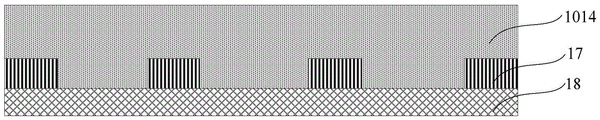
Optionally, as shown in fig. 7, the display panel 1 further includes a column spacer layer 17, and the column spacer layer 17 is disposed between the pixel defining structure 18 and the light-emitting functional layer 1014.
The columnar spacer layer 17 includes a plurality of columnar spacers arranged at intervals, and the columnar spacer layer 17 is used for supporting and protecting a Fine Metal Mask (FMM) used when forming the light emitting function layer 1014, so as to prevent the FMM from directly contacting the pixel defining structure 18, scratching the pixel defining structure 18 and causing electrostatic breakdown. The material of the columnar spacer may be photosensitive polyimide, for example.
As shown in fig. 1, the present invention further provides a manufacturing method of a display panel 1, the display panel 1 has a display area 10, the display area 10 includes a pixel area 101, an opening area 102, and an isolation area 103 located between the pixel area 101 and the opening area 102, and the isolation area 103 surrounds the opening area 102 for one turn.
As shown in fig. 8, the method for manufacturing the display panel 1 includes:
s10, as shown in fig. 9, at least one isolation pillar transition structure 104 is formed on the substrate 13 and located in the isolation region 103 by a dry etching process, wherein the isolation pillar transition structure 104 surrounds the opening region 102 for one turn.
The gas used during the dry etching process may be, for example, one or more of chlorine, helium, oxygen, and boron trichloride.
Fig. 9 is illustrated with the formation of two isolated pillar transition structures 104, each isolated pillar transition structure 104 being disposed around the open region 102.
S11, as shown in fig. 9, a protection pattern 1035 is formed on the upper surface of the pillar transition structure 104 away from the substrate 13.
The protective pattern 1035 may be formed by exposure, etching, or the like.
S12, as shown in fig. 9, performing a wet etching process on the isolation pillar transition structure 104 to form an isolation pillar 1031, wherein the isolation pillar 1031 has an i-shaped longitudinal section.
Nitric acid, for example, may be used as an etching liquid in the wet etching process.
The separator 1031 is i-shaped in longitudinal section. That is, as shown in fig. 4a, the isolation post 1031 includes a first isolation portion 1032, a second isolation portion 1033, and a third isolation portion 1034 that are sequentially stacked, and each side surface of the second isolation portion 1033 is inwardly recessed with respect to the first isolation portion 1032 and the third isolation portion 1034 in the thickness direction of the substrate 13.
Since external moisture and oxygen enter the display panel 1 after the opening region 102 is opened, and the light emitting functional layer 1014 in the pixel region 101 also extends into the isolation region 103, in order to prevent the moisture and oxygen from spreading along the light emitting functional layer 1014 in the isolation region 103 to the light emitting functional layer 1014 in the pixel region 101, the isolation pillar 1031 needs to be prepared in the isolation region 103. The purpose of the isolation posts 1031 is to break the light-emitting function layer 1014 when the light-emitting function layer 1014 is subsequently formed.
S13, as shown in fig. 9, a light emitting function layer 1014 is formed on the pixel region 101 and the isolation region 103 on the substrate 13 on which the isolation post 1031 is formed, and the light emitting function layer 1014 is broken at the side of the isolation post 1031 at the portion of the isolation region 103.
Illustratively, the light emitting function layer 1014 may be formed by evaporation using a fine metal mask.
The embodiment of the invention provides a preparation method of a display panel 1, and a display area 10 of the display panel 1 is provided with a pixel area 101, an opening area 102 and an isolation area 103. Firstly, the isolation pillar transition structure 104 and the protection pattern 1035 are prepared in the isolation region 103, and then the isolation pillar transition structure 104 is etched to form the i-shaped isolation pillar 1031, so that the problem that the disconnection capability of the isolation pillar 1031 to the light emitting function layer 1014 is insufficient when the actual length of the side of the isolation pillar 1031 far away from the substrate 13 is smaller than a preset value due to etching is avoided. In the above process, since the protective pattern 1035 is first formed and the structure of the protective pattern 1035 is not affected in the wet etching process, the probability that the light emitting function layer 1014 is broken at the side surface of the isolation post 1031 can be increased by using the entire protective pattern 1035 and the isolation post 1031. Secondly, the isolation post 1031 has an i-shaped longitudinal section, and when the light emitting functional layer 1014 is subjected to vapor deposition, the film layer is broken at the side surface of the isolation post 1031 due to the i-shaped structure. After the light-emitting functional layer 1014 is isolated, water vapor and oxygen entering from the opening region 102 can only spread to the light-emitting functional layer 1014 located in the isolation region 103 along the light-emitting functional layer 1014 extending to the opening region 102, and cannot continue to extend to the light-emitting functional layer 1014 located in the pixel region 101, so that the isolation column 1031 plays a role in isolating water vapor and oxygen.
Optionally, before forming the pillar transition structure 104, the method for manufacturing the display panel 1 further includes:
as shown in fig. 10, a first groove 151 is formed around the pillar transition structure 104 to be formed, and the first groove 151 is recessed toward the substrate 13 side with respect to the pillar transition structure 104 on the side close to the lower surface of the substrate 13.
The isolation pillar transition structure 104 and the first groove 151 may be located on a surface of the same insulating layer. Illustratively, the insulating layer may be an interlayer insulating layer 15.
The formation of the first groove 151 increases the height of the isolation post 1031 to be prepared later to a certain extent, so that the step difference of the disconnection of the light emitting function layer 1014 is increased when the light emitting function layer 1014 is evaporated, and the disconnection of the light emitting function layer 1014 on the side surface of the isolation post 1031 is easier.
Optionally, in step S10, forming at least one isolation pillar transition structure 104 on the substrate 13 and in the isolation region 103 by using a dry etching process, where the forming includes:
s101, as shown in fig. 11a, a first isolation film 1041, a second isolation film 1042 and a third isolation film 1043 are sequentially formed on a substrate 13 to cover an isolation region 103, and the first isolation film 1041, the second isolation film 1042 and the third isolation film 1043 are stacked; the materials of the first isolation film 1041 and the third isolation film 1043 are the same, the material of the second isolation film 1042 is different from the material of the first isolation film 1041 and the material of the third isolation film 1043, and the etching rates of the first isolation film 1041 and the third isolation film 1043 are greater than the etching rate of the second isolation film 1042.
S102, as shown in fig. 11b, etching the first isolation film 1041, the second isolation film 1042, and the third isolation film 1043 by a dry etching process to form at least one isolation pillar transition structure 104, where the isolation pillar transition structure 104 includes a first isolation pattern, a second isolation pattern, and a third isolation pattern.
For example, the material of the first isolation film 1041 and the third isolation film 1043 may be Ti (titanium), and the material of the second isolation film 1042 may be Al (aluminum), for example.
The etching rates of the first isolation film 1041 and the third isolation film 1043 are greater than the etching rate of the second isolation film 1042, so that the overall rectangular isolation column transition structure 104 can be etched into the isolation column 1031 with the longitudinal section in an i shape in the same etching solution. After the wet etching process is performed on the first, second, and third isolation patterns, a first isolation portion 1032, a second isolation portion 1033, and a third isolation portion 1034 are correspondingly formed.
Optionally, the first isolation film 1041, the second isolation film 1042, the third isolation film 1043, and the insulating layer may be etched by the same patterning process to obtain the isolation pillar transition structure 104 and the first groove 151. The number of times of the composition process is less, and the process is simpler.
Optionally, as shown in fig. 11b, the manufacturing method of the display panel 1 further includes forming a driving circuit 12 in the pixel region 101 and between the substrate 13 and the light-emitting functional layer 1014, where the driving circuit 12 includes the thin film transistor 14. The thin film transistor 14 includes a gate electrode 141, a source electrode 142, and a drain electrode 143; at least one of the first, second, and third isolation patterns is formed in synchronization with the gate electrode 141 or the source and drain electrodes 142 and 143.
The first, second, and third isolation patterns are formed in synchronization with the source and drain electrodes 142 and 143 in fig. 11b, for example, but not limited thereto.
At least one of the first, second, and third isolation patterns is formed in synchronization with the gate electrode 141 or the source and drain electrodes 142 and 143, and a manufacturing process is simple.
Optionally, forming the thin film transistor 14 and the spacer pillar transition structure 104 includes:
s103, as shown in fig. 11a, an active layer 144, a gate insulating layer 145, and a gate electrode 141 are sequentially formed on the substrate 13.
S104, as shown in fig. 11a, forming an interlayer insulating layer 15, where the interlayer insulating layer 15 includes a first via hole and a second via hole, and the first via hole and the second via hole expose portions of the active layer 144 on two sides of the gate 141, respectively.
S105, as shown in fig. 11a, a first isolation film 1041, a second isolation film 1042 and a third isolation film 1043 are sequentially formed on the interlayer insulating layer 15, and the first isolation film 1041, the second isolation film 1042 and the third isolation film 1043 all cover the pixel region 101 and the isolation region 103.
For example, the active layer 144 and the gate electrode 141 may be prepared by magnetron sputtering and patterning processes; the first, second, and third release films 1041, 1042, and 1043 may be prepared by coating; the interlayer insulating layer 15 may be prepared by high temperature vapor deposition and etching.
S106, as shown in fig. 11b, performing dry etching on the first isolation film 1041, the second isolation film 1042, and the third isolation film 1043, and forming a source electrode 142 and a drain electrode 143 in the pixel region 101, where the source electrode 142 and the drain electrode 143 are both of a three-layer structure and are in contact with the active layer 144 through a first via hole and a second via hole respectively; meanwhile, an isolation pillar transition structure 104 is formed in the isolation region 103.
The thin film transistor 14 formed by the preparation method is a top gate type thin film transistor, and the isolation pillar transition structure 104 is synchronously manufactured and formed in the process of preparing the top gate type thin film transistor, so that the process is simple.
Optionally, after forming the driving circuit 12 and before forming the light emitting function layer 1014, the method for manufacturing the display panel 1 further includes:
S14, as shown in fig. 11c, a planarization film 16 is formed to cover the pixel region 101 and the isolation region 103.
S15, as shown in fig. 11d, the planarization film 16 is etched by using the halftone mask to form a planarization pattern 160 covering the pixel region 101 and a protective pattern 1035.
Wherein the thickness of the planarization layer pattern 160 is greater than the thickness of the protective pattern 1035.
Taking polyimide as an example of photosensitive material for forming the planarization film 16, the polyimide is exposed by using a halftone mask and developed to form a polyimide completely-remaining portion, a polyimide semi-remaining portion, and a polyimide completely-removed portion. The polyimide completely remaining portion corresponds to the planarization layer pattern 160, the polyimide half remaining portion corresponds to the protective pattern 1035, and the polyimide completely removed portion corresponds to other portions, such as between the planarization layer pattern 160 and the isolation pillar 1031, between the isolation pillar 1031 and the first retaining wall 1036, and the like.
The halftone mask utilizes partial light transmittance of the grating, can incompletely expose the photoresist material, and can determine the amount of light to transmit according to the height of the required film layer, so that the halftone mask can be used for manufacturing the flat layer pattern 160 and the protective pattern 1035 with different thicknesses.
The thickness of the protective pattern 1035 is smaller than the thickness of the planarization pattern 160, so that the formation of the protective pattern 1035 and the isolation bar 1031 into a sharp end is prevented from being detrimental to the subsequent fabrication of the light-emitting function layer 1014 and other layers on the upper side of the light-emitting function layer 1014.
Alternatively, as shown in fig. 11d, a raised portion 161 located in the isolation region 103 is also formed simultaneously with the formation of the planarization layer pattern 160.
After the formation of the planarization layer pattern 160, the protective pattern 1035, and the raised portion 161, and before the formation of the light emitting function layer 1014, the method of manufacturing the display panel 1 further includes:
as shown in fig. 12a, an anode 1012 is formed in the pixel region 101.
Forming a pixel defining structure 18 on the substrate 13 on which the anode 1012 is formed, and simultaneously forming a first retaining wall 1036 and a second retaining wall 1037 in the isolation region 103, the first retaining wall 1036 and the second retaining wall 1037 surrounding the opening region 102 one turn; the first blocking wall 1036 is positioned between the isolation column 1031 and the second blocking wall 1037, and the second blocking wall 1037 is formed above the raised portion 161.
The raised portion 161 is used to support the second barrier 1037 to be subsequently formed, and the raised portion 161 and the planarization layer pattern 160 are simultaneously formed, so that the process for forming the raised portion 161 is simple.
Optionally, as shown in fig. 10, the method further includes: the second recess 152 is formed around the first retaining wall 1036 and/or the second retaining wall 1037, and the second recess 152 is recessed toward the substrate 13 side with respect to the lower surface side of the first retaining wall 1036 and/or the second retaining wall 1037 close to the substrate 13.
As shown in fig. 11a to 11d, the second groove 152 may be formed simultaneously with the first groove 151.
As shown in fig. 12b, after forming the light emitting function layer 1014, the method of manufacturing the display panel 1 further includes: a cathode 1013 is formed.
Among them, the anode 1012, the light emitting function layer 1014, and the cathode 1013 at each sub-pixel region in the pixel region 101 constitute the light emitting device 1011.
The anode 1012 and the cathode 1013 in the light-emitting device 1011 are used to supply an electric field to the light-emitting functional layer 1014, so that the light-emitting layer 1015 in the light-emitting functional layer 1014 emits light by the electric field.
As shown in fig. 2a, 2b and 2c, after forming the cathode 1013, the method for manufacturing the display panel 1 further includes forming a first inorganic encapsulation layer 19, forming an organic layer 20 on the first inorganic encapsulation layer 19, and forming a second inorganic encapsulation layer 21 on the organic layer 20.
For example, the first inorganic encapsulating layer 19 and the second inorganic encapsulating layer 21 may be formed by low-temperature vapor deposition or the like, and the organic layer 20 may be formed by inkjet printing or the like.
The embodiment of the invention also provides a display panel 1, and the display panel 1 is obtained by using the preparation method of the display panel 1.
The isolation posts 1031 and the protection patterns 1035 are provided on the substrate of the display panel 1, and the display panel 1 has a simple structure and is easy to manufacture.
The present invention also provides a display device including a display panel 1 and a driving circuit for driving the display panel 1. The display panel 1 is various display panels 1 as described above, and the driving circuit includes, for example, a source driver and a timing controller. The display device has the same advantages as the display panel 1, and thus the description is omitted.
The above description is only for the specific embodiments of the present invention, but the scope of the present invention is not limited thereto, and any person skilled in the art can easily conceive of the changes or substitutions within the technical scope of the present invention, and all the changes or substitutions should be covered within the scope of the present invention. Therefore, the protection scope of the present invention shall be subject to the protection scope of the appended claims.