CN109524443B - An OLED substrate and an OLED display device - Google Patents
An OLED substrate and an OLED display device Download PDFInfo
- Publication number
- CN109524443B CN109524443B CN201811543965.XA CN201811543965A CN109524443B CN 109524443 B CN109524443 B CN 109524443B CN 201811543965 A CN201811543965 A CN 201811543965A CN 109524443 B CN109524443 B CN 109524443B
- Authority
- CN
- China
- Prior art keywords
- layer
- sub
- electrode
- pad
- oled substrate
- Prior art date
- Legal status (The legal status is an assumption and is not a legal conclusion. Google has not performed a legal analysis and makes no representation as to the accuracy of the status listed.)
- Active
Links
Images


Classifications
-
- H—ELECTRICITY
- H10—SEMICONDUCTOR DEVICES; ELECTRIC SOLID-STATE DEVICES NOT OTHERWISE PROVIDED FOR
- H10K—ORGANIC ELECTRIC SOLID-STATE DEVICES
- H10K59/00—Integrated devices, or assemblies of multiple devices, comprising at least one organic light-emitting element covered by group H10K50/00
- H10K59/10—OLED displays
- H10K59/12—Active-matrix OLED [AMOLED] displays
- H10K59/122—Pixel-defining structures or layers, e.g. banks
-
- H—ELECTRICITY
- H10—SEMICONDUCTOR DEVICES; ELECTRIC SOLID-STATE DEVICES NOT OTHERWISE PROVIDED FOR
- H10K—ORGANIC ELECTRIC SOLID-STATE DEVICES
- H10K50/00—Organic light-emitting devices
- H10K50/80—Constructional details
- H10K50/805—Electrodes
- H10K50/82—Cathodes
- H10K50/824—Cathodes combined with auxiliary electrodes
-
- H—ELECTRICITY
- H10—SEMICONDUCTOR DEVICES; ELECTRIC SOLID-STATE DEVICES NOT OTHERWISE PROVIDED FOR
- H10K—ORGANIC ELECTRIC SOLID-STATE DEVICES
- H10K50/00—Organic light-emitting devices
- H10K50/80—Constructional details
- H10K50/84—Passivation; Containers; Encapsulations
- H10K50/844—Encapsulations
-
- H—ELECTRICITY
- H10—SEMICONDUCTOR DEVICES; ELECTRIC SOLID-STATE DEVICES NOT OTHERWISE PROVIDED FOR
- H10K—ORGANIC ELECTRIC SOLID-STATE DEVICES
- H10K59/00—Integrated devices, or assemblies of multiple devices, comprising at least one organic light-emitting element covered by group H10K50/00
- H10K59/10—OLED displays
- H10K59/12—Active-matrix OLED [AMOLED] displays
- H10K59/121—Active-matrix OLED [AMOLED] displays characterised by the geometry or disposition of pixel elements
-
- H—ELECTRICITY
- H10—SEMICONDUCTOR DEVICES; ELECTRIC SOLID-STATE DEVICES NOT OTHERWISE PROVIDED FOR
- H10K—ORGANIC ELECTRIC SOLID-STATE DEVICES
- H10K59/00—Integrated devices, or assemblies of multiple devices, comprising at least one organic light-emitting element covered by group H10K50/00
- H10K59/10—OLED displays
- H10K59/12—Active-matrix OLED [AMOLED] displays
- H10K59/124—Insulating layers formed between TFT elements and OLED elements
-
- H—ELECTRICITY
- H10—SEMICONDUCTOR DEVICES; ELECTRIC SOLID-STATE DEVICES NOT OTHERWISE PROVIDED FOR
- H10K—ORGANIC ELECTRIC SOLID-STATE DEVICES
- H10K59/00—Integrated devices, or assemblies of multiple devices, comprising at least one organic light-emitting element covered by group H10K50/00
- H10K59/10—OLED displays
- H10K59/12—Active-matrix OLED [AMOLED] displays
- H10K59/131—Interconnections, e.g. wiring lines or terminals
- H10K59/1315—Interconnections, e.g. wiring lines or terminals comprising structures specially adapted for lowering the resistance
-
- H—ELECTRICITY
- H10—SEMICONDUCTOR DEVICES; ELECTRIC SOLID-STATE DEVICES NOT OTHERWISE PROVIDED FOR
- H10K—ORGANIC ELECTRIC SOLID-STATE DEVICES
- H10K59/00—Integrated devices, or assemblies of multiple devices, comprising at least one organic light-emitting element covered by group H10K50/00
- H10K59/80—Constructional details
- H10K59/805—Electrodes
- H10K59/8052—Cathodes
- H10K59/80522—Cathodes combined with auxiliary electrodes
-
- H—ELECTRICITY
- H10—SEMICONDUCTOR DEVICES; ELECTRIC SOLID-STATE DEVICES NOT OTHERWISE PROVIDED FOR
- H10K—ORGANIC ELECTRIC SOLID-STATE DEVICES
- H10K71/00—Manufacture or treatment specially adapted for the organic devices covered by this subclass
-
- H—ELECTRICITY
- H10—SEMICONDUCTOR DEVICES; ELECTRIC SOLID-STATE DEVICES NOT OTHERWISE PROVIDED FOR
- H10K—ORGANIC ELECTRIC SOLID-STATE DEVICES
- H10K59/00—Integrated devices, or assemblies of multiple devices, comprising at least one organic light-emitting element covered by group H10K50/00
- H10K59/10—OLED displays
- H10K59/12—Active-matrix OLED [AMOLED] displays
- H10K59/1201—Manufacture or treatment
-
- H—ELECTRICITY
- H10—SEMICONDUCTOR DEVICES; ELECTRIC SOLID-STATE DEVICES NOT OTHERWISE PROVIDED FOR
- H10K—ORGANIC ELECTRIC SOLID-STATE DEVICES
- H10K59/00—Integrated devices, or assemblies of multiple devices, comprising at least one organic light-emitting element covered by group H10K50/00
- H10K59/80—Constructional details
- H10K59/87—Passivation; Containers; Encapsulations
- H10K59/873—Encapsulations
Landscapes
- Engineering & Computer Science (AREA)
- Microelectronics & Electronic Packaging (AREA)
- Physics & Mathematics (AREA)
- Optics & Photonics (AREA)
- Geometry (AREA)
- Manufacturing & Machinery (AREA)
- Electroluminescent Light Sources (AREA)
- Devices For Indicating Variable Information By Combining Individual Elements (AREA)
Abstract
本发明实施例提供一种OLED基板及OLED显示装置,涉及显示技术领域,可改善第二电极层电阻过大导致的IR‑drop问题。OLED基板的显示区划分为多个发光区和非发光区,所述非发光区包括第一连接区;所述OLED基板包括:依次设置于衬底上的第一电极层、像素界定层、发光功能层和第二电极层;所述像素界定层位于所述非发光区,所述像素界定层限定出多个所述发光区;所述第一电极层包括多个第一电极,每个所述第一电极位于一个所述发光区中;所述像素界定层在所述第一连接区镂空;所述OLED基板还包括:设置在所述第一连接区的导电结构,所述导电结构位于所述发光功能层远离所述衬底的一侧,且与所述第二电极层接触。
This invention provides an OLED substrate and an OLED display device, relating to the field of display technology, which can improve the IR-drop problem caused by excessive resistance of the second electrode layer. The display area of the OLED substrate is divided into multiple light-emitting and non-light-emitting areas, the non-light-emitting areas including a first connection area; the OLED substrate includes: a first electrode layer, a pixel defining layer, a light-emitting functional layer, and a second electrode layer sequentially disposed on a substrate; the pixel defining layer is located in the non-light-emitting area and defines multiple light-emitting areas; the first electrode layer includes multiple first electrodes, each first electrode located in one of the light-emitting areas; the pixel defining layer is hollowed out in the first connection area; the OLED substrate further includes: a conductive structure disposed in the first connection area, the conductive structure being located on the side of the light-emitting functional layer away from the substrate and in contact with the second electrode layer.
Description
技术领域technical field
本发明涉及显示技术领域,尤其涉及一种OLED基板及OLED显示装置。The present invention relates to the field of display technology, and in particular, to an OLED substrate and an OLED display device.
背景技术Background technique
OLED(Organic Light Emitting Diode,有机电致发光二极管)显示装置由于具有自发光、响应速度快、亮度高、全视角、可柔性显示等一系列优点,因而成为目前极具竞争力和发展前景的下一代显示装置。OLED (Organic Light Emitting Diode, organic electroluminescent diode) display device has a series of advantages such as self-luminous, fast response, high brightness, full viewing angle, flexible display, etc. Generation Display.
OLED显示装置包括底发射型结构和顶发射型结构。随着市场对高分辨率产品需求的增大,底发射型OLED显示装置由于受开口率的限制,难以实现高分辨率的显示需求,而顶发射型OLED显示装置具有开口率大的特性,更有利于实现高分辨率显示,因而目前顶发射型OLED显示装置受到了广泛的关注。The OLED display device includes a bottom emission type structure and a top emission type structure. With the increasing demand for high-resolution products in the market, it is difficult for bottom-emission OLED display devices to achieve high-resolution display due to the limitation of aperture ratio, while top-emission OLED display devices have the characteristics of large aperture ratio, and more It is beneficial to realize high-resolution display, so currently top-emission OLED display devices have received extensive attention.
顶发射型OLED显示装置的阴极通常是通过溅射或蒸镀沉积一层透明或半透明的导电材料形成,阴极的厚度越薄,光的透过率越高,越有利于提高OLED显示装置的亮度。然而,阴极的厚度越薄,阴极的电阻越大,而阴极电阻过大带来的电压降(IR-drop)会严重影响OLED显示装置的显示效果。这是因为OLED显示装置中心距离OLED显示装置边缘设置的信号输入口较远,而阴极电阻过大带来的电压降会导致电流传输至OLED显示装置中心时降低很多,从而导致OLED显示装置边缘和中间的亮度不一致,即OLED显示装置中间暗边缘亮。The cathode of the top emission OLED display device is usually formed by depositing a layer of transparent or semi-transparent conductive material by sputtering or evaporation. brightness. However, the thinner the thickness of the cathode, the greater the resistance of the cathode, and the voltage drop (IR-drop) caused by the excessively large cathode resistance will seriously affect the display effect of the OLED display device. This is because the center of the OLED display device is far away from the signal input port set at the edge of the OLED display device, and the voltage drop caused by the excessive cathode resistance will reduce the current transmission to the center of the OLED display device. The brightness in the middle is inconsistent, that is, the middle dark edge of the OLED display device is bright.
发明内容SUMMARY OF THE INVENTION
本发明的实施例提供一种OLED基板及OLED显示装置,可改善第二电极层电阻过大导致的IR-drop问题。Embodiments of the present invention provide an OLED substrate and an OLED display device, which can improve the IR-drop problem caused by the excessive resistance of the second electrode layer.
为达到上述目的,本发明的实施例采用如下技术方案:To achieve the above object, the embodiments of the present invention adopt the following technical solutions:
本发明的一些实施例提供一种OLED基板,显示区划分为多个发光区和非发光区,所述非发光区包括第一连接区;所述OLED基板包括:依次设置于衬底上的第一电极层、像素界定层、发光功能层和第二电极层;所述像素界定层位于所述非发光区,所述像素界定层限定出多个所述发光区;所述第一电极层包括多个第一电极,每个所述第一电极位于一个所述发光区中;所述像素界定层在所述第一连接区镂空;所述OLED基板还包括:设置在所述第一连接区的导电结构,所述导电结构位于所述发光功能层远离所述衬底的一侧,且与所述第二电极层接触。Some embodiments of the present invention provide an OLED substrate, wherein a display area is divided into a plurality of light-emitting areas and a non-light-emitting area, the non-light-emitting area includes a first connection area; the OLED substrate includes: a first connection area arranged on the substrate in sequence an electrode layer, a pixel definition layer, a light-emitting functional layer and a second electrode layer; the pixel definition layer is located in the non-light-emitting area, and the pixel definition layer defines a plurality of the light-emitting areas; the first electrode layer includes a plurality of first electrodes, each of the first electrodes is located in one of the light-emitting regions; the pixel defining layer is hollowed out in the first connection region; the OLED substrate further comprises: disposed in the first connection region The conductive structure is located on the side of the light-emitting functional layer away from the substrate, and is in contact with the second electrode layer.
在一些实施例中,所述发光功能层在所述第一连接区的边界断开,且所述导电结构远离所述衬底的表面高于所述像素界定层远离所述衬底的表面。In some embodiments, the light-emitting functional layer is disconnected at the boundary of the first connection region, and a surface of the conductive structure away from the substrate is higher than a surface of the pixel defining layer away from the substrate.
在一些实施例中,所述导电结构位于所述发光功能层和所述第二电极层之间;或者,所述导电结构位于所述第二电极层远离所述发光功能层的一侧。In some embodiments, the conductive structure is located between the light-emitting functional layer and the second electrode layer; or, the conductive structure is located on a side of the second electrode layer away from the light-emitting functional layer.
在一些实施例中,所述非发光区还包括第二连接区,所述第二连接区与所述第一连接区相邻;所述OLED基板还包括设置在所述第二连接区的垫高层和第一辅助电极,所述第一辅助电极覆盖所述垫高层的侧面和远离所述衬底的表面;所述导电结构与所述第一辅助电极中位于所述垫高层侧面的部分接触。In some embodiments, the non-light-emitting area further includes a second connection area adjacent to the first connection area; the OLED substrate further includes a pad disposed in the second connection area a high layer and a first auxiliary electrode, the first auxiliary electrode covers the side surface of the pad layer and the surface away from the substrate; the conductive structure is in contact with the part of the first auxiliary electrode located on the side surface of the pad layer .
在一些实施例中,所述像素界定层在所述第二连接区镂空;所述第一辅助电极与所述第一电极同层同材料。In some embodiments, the pixel defining layer is hollowed out in the second connection region; the first auxiliary electrode and the first electrode are of the same layer and the same material.
在一些实施例中,所述OLED基板还包括薄膜晶体管以及设置在所述薄膜晶体管和所述第一电极层之间的平坦层;所述薄膜晶体管包括源极、漏极、有源层、栅极以及栅绝缘层,所述漏极与所述第一电极电连接;所述垫高层包括第一子垫高层、第二子垫高层、第三子垫高层、第四子垫高层和第五子垫高层中的至少一层;所述第一子垫高层、所述第二子垫高层、所述第三子垫高层、所述第四子垫高层和第五子垫高层层叠设置;所述第一子垫高层与所述有源层同层同材料;所述栅绝缘层位于所述第二连接区的部分构成所述垫高层中的所述第二子垫高层;所述第三子垫高层与所述栅极同层同材料;所述第四子垫高层与所述源极、所述漏极同层同材料;所述平坦层位于所述第二连接区的部分构成所述垫高层中的所述第五子垫高层。In some embodiments, the OLED substrate further includes a thin film transistor and a flat layer disposed between the thin film transistor and the first electrode layer; the thin film transistor includes a source electrode, a drain electrode, an active layer, a gate electrode electrode and a gate insulating layer, the drain electrode is electrically connected to the first electrode; the pad layer includes a first sub pad layer, a second sub pad layer, a third sub pad layer, a fourth sub pad layer and a fifth sub pad layer at least one layer in the sub-cushion layer; the first sub-cushion layer, the second sub-cushion layer, the third sub-cushion layer, the fourth sub-cushion layer and the fifth sub-cushion layer are stacked; the the first sub-pad layer and the active layer are of the same layer and the same material; the part of the gate insulating layer located in the second connection region constitutes the second sub-pad layer in the pad layer; the third sub-pad layer The sub-pad layer and the gate are of the same layer and the same material; the fourth sub-pad layer, the source electrode and the drain electrode are of the same layer and the same material; the part of the flat layer located in the second connection region constitutes a the fifth sub-cushion layer in the cushion layer.
在一些实施例中,所述第五子垫高层的侧面和所述第五子垫高层靠近所述第二电极层的表面通过圆弧段连接。In some embodiments, the side surface of the fifth sub-layer layer and the surface of the fifth sub-layer layer close to the second electrode layer are connected by arc segments.
在一些实施例中,所述薄膜晶体管还包括层间介电层;所述层间介电层在所述第一连接区镂空;所述层间介电层位于所述第二连接区的部分构成所述垫高层中的第六子垫高层。In some embodiments, the thin film transistor further includes an interlayer dielectric layer; the interlayer dielectric layer is hollowed out in the first connection region; the interlayer dielectric layer is located in a part of the second connection region A sixth sub-cushion layer in the cushion layer is formed.
在一些实施例中,所述第六子垫高层的侧面为倾斜面,所述第六子垫高层中靠近所述第二电极层表面的面积大于远离所述第二电极层表面的面积。In some embodiments, the side surfaces of the sixth sub-layer are inclined surfaces, and the area of the sixth sub-layer close to the surface of the second electrode layer is larger than the area away from the surface of the second electrode layer.
在一些实施例中,所述OLED基板还包括设置在所述薄膜晶体管和所述平坦层之间的钝化层;所述钝化层位于所述第二连接区的部分构成所述垫高层中的第七子垫高层。In some embodiments, the OLED substrate further includes a passivation layer disposed between the thin film transistor and the flat layer; the passivation layer is located in the second connection region and a part of the pad layer is formed The seventh sub-cushion layer.
在一些实施例中,所述第七子垫高层的侧面为倾斜面,所述第七子垫高层中靠近所述第二电极层表面的面积大于远离所述第二电极层表面的面积。In some embodiments, the side surface of the seventh sub-layer layer is an inclined surface, and the area of the seventh sub-layer layer close to the surface of the second electrode layer is larger than the area away from the surface of the second electrode layer.
在一些实施例中,所述导电结构为多个;所述导电结构设置在所述垫高层的两侧,所述第一辅助电极中位于所述垫高层侧面的部分与设置在所述垫高层两侧的所述导电结构均接触。In some embodiments, there are a plurality of the conductive structures; the conductive structures are arranged on both sides of the pad layer, and the portion of the first auxiliary electrode located on the side surface of the pad layer and the portion of the first auxiliary electrode arranged on the pad layer The conductive structures on both sides are in contact.
在一些实施例中,所述导电结构的形状为沿平行于所述衬底的任一条边延伸的条状。In some embodiments, the conductive structure is in the shape of a strip extending parallel to any side of the substrate.
在一些实施例中,所述导电结构的形状为点状。In some embodiments, the shape of the conductive structure is dot-like.
本发明的实施例还提供一种OLED显示装置,包括OLED基板和用于封装所述OLED基板的封装层;所述OLED基板为上述的OLED基板。Embodiments of the present invention further provide an OLED display device, comprising an OLED substrate and an encapsulation layer for encapsulating the OLED substrate; the OLED substrate is the above-mentioned OLED substrate.
本发明实施例提供一种OLED基板及OLED显示装置,由于OLED基板包括导电结构,且导电结构与第二电极层接触,因而导电结构可以降低第二电极层的电阻,从而改善了第二电极层电阻过大导致的IR-drop问题。Embodiments of the present invention provide an OLED substrate and an OLED display device. Since the OLED substrate includes a conductive structure, and the conductive structure is in contact with the second electrode layer, the conductive structure can reduce the resistance of the second electrode layer, thereby improving the second electrode layer. IR-drop problem caused by excessive resistance.
附图说明Description of drawings
为了更清楚地说明本发明实施例或相关技术中的技术方案,下面将对实施例或相关技术描述中所需要使用的附图作简单地介绍,显而易见地,下面描述中的附图仅仅是本发明的一些实施例,对于本领域普通技术人员来讲,在不付出创造性劳动的前提下,还可以根据这些附图获得其他的附图。In order to more clearly illustrate the technical solutions in the embodiments of the present invention or related technologies, the following briefly introduces the accompanying drawings required for the description of the embodiments or related technologies. Obviously, the accompanying drawings in the following description are only the For some embodiments of the invention, for those of ordinary skill in the art, other drawings can also be obtained according to these drawings without any creative effort.
图1为相关技术提供的一种OLED显示装置的结构示意图;1 is a schematic structural diagram of an OLED display device provided by the related art;
图2为相关技术提供的一种OLED基板的结构示意图;FIG. 2 is a schematic structural diagram of an OLED substrate provided by the related art;
图3为本发明实施例提供一种OLED基板不同区的划分示意图;3 is a schematic diagram of division of different regions of an OLED substrate according to an embodiment of the present invention;
图4a为本发明实施例提供一种OLED基板的结构示意图一;FIG. 4a is a schematic structural diagram 1 of an OLED substrate provided by an embodiment of the present invention;
图4b为本发明实施例提供一种OLED基板的结构示意图二;4b is a second structural schematic diagram of an OLED substrate provided by an embodiment of the present invention;
图5为本发明实施例提供一种OLED基板的结构示意图三;FIG. 5 is a third structural schematic diagram of an OLED substrate provided by an embodiment of the present invention;
图6为本发明实施例提供一种OLED基板的结构示意图四;FIG. 6 is a schematic diagram 4 of the structure of an OLED substrate provided by an embodiment of the present invention;
图7为本发明实施例提供一种OLED基板的结构示意图五;7 is a schematic structural diagram 5 of an OLED substrate provided by an embodiment of the present invention;
图8a为本发明实施例提供一种OLED基板的结构示意图六;FIG. 8a is a sixth structural schematic diagram of an OLED substrate according to an embodiment of the present invention;
图8b为本发明实施例提供一种OLED基板的结构示意图七;FIG. 8b is a seventh structural schematic diagram of an OLED substrate provided by an embodiment of the present invention;
图9为本发明实施例提供一种OLED基板的结构示意图八;FIG. 9 is a schematic structural diagram eight of an OLED substrate provided by an embodiment of the present invention;
图10a为本发明实施例提供一种OLED基板的结构示意图九;10a is a schematic structural diagram 9 of an OLED substrate according to an embodiment of the present invention;
图10b为本发明实施例提供一种OLED基板的结构示意图十;FIG. 10b is a schematic structural diagram ten of an OLED substrate according to an embodiment of the present invention;
图11为本发明实施例提供一种OLED基板的结构示意图十一;FIG. 11 is a schematic structural diagram eleventh of an OLED substrate provided by an embodiment of the present invention;
图12为本发明实施例提供一种OLED显示装置的结构示意图。FIG. 12 is a schematic structural diagram of an OLED display device according to an embodiment of the present invention.
附图标记:Reference number:
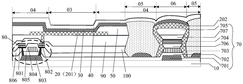
01-显示区;02-非显示区;03-发光区;04-非发光区;05-第一连接区;06-第二连接区;1-封装基板;2-辅助电极;3-阴极;4、10-衬底;5-阳极;6、30-发光功能层;7、50-像素界定层;8-绝缘图案;20-第一电极层;201-第一电极;202-第一辅助电极;40-第二电极层;60-导电结构;70-垫高层;701-第一子垫高层;702-第二子垫高层;703-第三子垫高层;704-第四子垫高层;705-第五子垫高层;706-第六子垫高层;707-第七子垫高层;80-薄膜晶体管;801-源极;802-漏极;803-有源层;804-栅极;805-栅绝缘层;806-层间介电层;90-平坦层;100-钝化层;110-OLED基板;120-封装层。01-display area; 02-non-display area; 03-light-emitting area; 04-non-light-emitting area; 05-first connection area; 06-second connection area; 1-package substrate; 2-auxiliary electrode; 3-cathode; 4, 10 - substrate; 5 - anode; 6, 30 - light-emitting functional layer; 7, 50 - pixel defining layer; 8 - insulating pattern; 20 - first electrode layer; 201 - first electrode; 202 - first auxiliary electrode; 40-second electrode layer; 60-conductive structure; 70-pad layer; 701-first subpad layer; 702-second subpad layer; 703-third subpad layer; 704-fourth subpad layer ; 705 - the fifth sub-pad layer; 706 - the sixth sub-pad layer; 707 - the seventh sub-pad layer; 80 - thin film transistor; 801 - source; 802 - drain; 803 - active layer; 804 - gate 805-gate insulating layer; 806-interlayer dielectric layer; 90-flat layer; 100-passivation layer; 110-OLED substrate; 120-encapsulation layer.
具体实施方式Detailed ways
下面将结合本发明实施例中的附图,对本发明实施例中的技术方案进行清楚、完整地描述,显然,所描述的实施例仅仅是本发明一部分实施例,而不是全部的实施例。基于本发明中的实施例,本领域普通技术人员在没有做出创造性劳动前提下所获得的所有其他实施例,都属于本发明保护的范围。The technical solutions in the embodiments of the present invention will be clearly and completely described below with reference to the accompanying drawings in the embodiments of the present invention. Obviously, the described embodiments are only a part of the embodiments of the present invention, but not all of the embodiments. Based on the embodiments of the present invention, all other embodiments obtained by those of ordinary skill in the art without creative efforts shall fall within the protection scope of the present invention.
为了改善OLED显示装置因阴极电阻过大导致的IR-drop问题,相关技术中,主要采用两种方式。第一种,在透明的阴极上增设辅助电极。示例的,如图1所示,在封装基板1上设置增设导电层或网格状导线作为辅助电极2,辅助电极2与透明的阴极3接触,通过辅助电极2增加阴极3的导电率,从而降低阴极3的电阻。然而,为了实现辅助电极2与阴极3的接触,未使用薄膜封装层对OLED器件(OLED器件包括设置在衬底4上的阳极5、发光功能层6、阴极3以及用于间隔阳极5的像素界定层7)进行封装,从而导致了OLED器件劣化的风险增加。In order to improve the IR-drop problem caused by the excessive cathode resistance of the OLED display device, two methods are mainly adopted in the related art. The first is to add auxiliary electrodes on the transparent cathode. Exemplarily, as shown in FIG. 1 , an additional conductive layer or grid-like wire is provided on the
第二种,在透明的阴极3下增设辅助电极2。示例的,如图2所示,在位于非发光区的像素界定层7上增设绝缘图案8和辅助电极2。然而该方案中阴极3只能与辅助电极2的侧面接触,辅助电极2的大部分表面被发光功能层6覆盖,这样一来降低阴极3电阻的效果不明显,此外,绝缘图案8和辅助电极2的形成需要额外增加两次成膜和光刻工艺,导致了OLED显示装置的制备工艺复杂。The second is to add an
基于此,本发明实施例提供一种OLED基板,如图3所示,OLED基板划分为显示区01和非显示区02,显示区01划分为多个发光区03和非发光区04,非发光区04包括第一连接区05。此处,对于第一连接区05的位置不进行限定,在不影响OLED基板正常使用的前提下,第一连接区05可以在非发光区04任意设置。Based on this, an embodiment of the present invention provides an OLED substrate. As shown in FIG. 3 , the OLED substrate is divided into a
如图4a和图4b所示,OLED基板包括:依次设置于衬底10上的第一电极层20、像素界定层(Pixel Definition Layer,简称PDL)50、发光功能层(Electroluminescent,简称EL)30和第二电极层40;像素界定层50位于非发光区04,像素界定层50限定出多个发光区03,即像素界定层50包括多个开口区域,一个开口区域对应一个发光区03;第一电极层20包括多个第一电极(即像素电极)201,每个第一电极201位于一个发光区03中;像素界定层50在第一连接区05镂空。As shown in FIG. 4 a and FIG. 4 b , the OLED substrate includes: a
OLED基板还包括:设置在第一连接区05的导电结构60,导电结构60位于发光功能层30远离衬底10的一侧,且与第二电极层40接触。The OLED substrate further includes: a
此处,对于衬底10的材质不进行限定,例如可以为玻璃。Here, the material of the
在一些实施例中,第一电极层20为阳极,第二电极层40为阴极。在另一些实施例中,第一电极层20为阴极,第二电极层40为阳极。In some embodiments, the
对于第一电极层20的材料不进行限定,示例的,第一电极层20的材料可以选用Ag(银)、Al(铝)以及ITO(Indium Tin Oxide,氧化铟锡)中的一种或几种。此外,第一电极层20可以是单层结构,也可以是多层叠层结构。对于形成第一电极层20的具体工艺不进行限定,示例的,可以先沉积如利用PVD(Physical Vapor Deposition,物理气相沉积)工艺沉积一层或层叠的多层导电薄膜,再通过光刻和刻蚀工艺制作出图案化的第一电极201。The material of the
对于第二电极层40的材料不进行限定,由于发光功能层30发出的光要从第二电极层40出射,因而第二电极层40的材料为透明材料。第二电极层40的材料例如可以选自ITO或IZO(Indium Zinc Oxide,氧化铟锌)中的至少一种。此处,可以采用蒸镀工艺在发光功能层30上蒸镀一层第二电极层40。The material of the
在一些实施例中,发光功能层30仅包括发光层。在另一些实施例中,发光功能层30除包括发光层外,还包括电子传输层(election transporting layer,简称ETL)、电子注入层(election injection layer,简称EIL)、空穴传输层(hole transporting layer,简称HTL)以及空穴注入层(hole injection layer,简称HIL)中的至少一层。此处,可以采用蒸镀工艺在像素界定层50上蒸镀发光功能层30。In some embodiments, the light-emitting
此处,对于制作像素界定层50的工艺不进行限定,示例的,可以先在第一电极层20上形成(例如采用旋涂、转印或喷墨打印工艺中的一种)一层像素界定层薄膜,再通过光刻工艺对像素界定层薄膜进行图案化,从而形成像素界定层50。Here, the process of fabricating the
其中,对于导电结构60的材料不进行限定,以能导电为准。由于导电结构60设置在第一连接区05,而第一连接区05位于非发光区04,因而导电结构60的材料可以为透明材料,也可以为非透明材料。例如,导电结构60的材料可以为导电聚合物、金属、导电银浆或导电胶中的至少一种。The material of the
在此基础上,对于如何在第一连接区05形成导电结构60不进行限定,例如,可以采用喷墨打印(Ink-Jet Printing,简称IJP)工艺在第一连接区05形成导电结构60。又例如,可以采用丝网印刷工艺在第一连接区05形成导电结构60。On this basis, how to form the
需要说明的是,导电结构60位于发光功能层30远离衬底10的一侧,在一些实施例中,如图4a所示,导电结构60位于第二电极层40远离发光功能层30的一侧。此时,先形成第二电极层40,再形成导电结构60。在另一些实施例中,如图4b所示,导电结构60位于发光功能层30和第二电极层40之间。此时,先形成导电结构60,再形成第二电极层40。It should be noted that the
此外,像素界定层50在第一连接区05镂空,即像素界定层50在第一连接区05具有凹槽(也称凹形落差区),在第一连接区05(即在凹槽中)设置发光功能层30时,在一些实施例中,如图4a和图4b所示,发光功能层30在第一连接区05的边界断开。在另一些实施例中,发光功能层30在第一连接区05的边界未断开。凹槽的深度越大,发光功能层30越容易断开。如图4a所示,当导电结构60位于第二电极层40远离发光功能层30的一侧时,第二电极层40可以在第一连接区05的边界断开,也可以在第一连接区05的边界连续,即不断开。In addition, the
本领域技术人员应该明白,导电结构60与第二电极层40的接触面积越大,越有利于降低第二电极层40的电阻。本发明实施例优选的,第一连接区05为条状,这样便可以将导电结构60设置为条状,从而可以增加导电结构60与第二电极层40的接触面积。Those skilled in the art should understand that the larger the contact area between the
虽然像素界定层50在第一连接区05镂空,但是由于第一连接区05设置有导电结构60,因而无需考虑第二电极层40在第一连接区05连续差的风险,就能够保证第二电极层40与导电结构60电连接。Although the
本发明实施例提供一种OLED基板,由于OLED基板包括导电结构60,且导电结构60与第二电极层40接触,因而导电结构60可以降低第二电极层40的电阻,从而改善了第二电极层40电阻过大导致的IR-drop问题。An embodiment of the present invention provides an OLED substrate. Since the OLED substrate includes a
在此基础上,相对于相关技术中的第一种方式,由于导电结构60(相当于辅助电极2)设置在OLED基板上,因而在能够降低第二电极层40电阻的同时,不会影响OLED基板的封装。相对于相关技术中的第二种方式,由于导电结构60设置在第二电极层40上,或者第二电极层40设置在导电结构60上,因而导电结构60与第二电极层40的接触面积较大,可以有效地降低第二电极层40的电阻。此外,利用IJP工艺或丝网印刷工艺便可以形成导电结构60,无需光刻工艺,因而不会增加制备OLED基板的工艺复杂度。On this basis, compared with the first method in the related art, since the conductive structure 60 (equivalent to the auxiliary electrode 2 ) is disposed on the OLED substrate, the resistance of the
优选的,如图4a和图4b所示,发光功能层30在第一连接区05的边界断开,且导电结构60远离衬底10的表面(即附图中的上表面)高于像素界定层50远离衬底10的表面。Preferably, as shown in FIG. 4a and FIG. 4b, the light-emitting
需要说明的是,在形成发光功能层30时,第一连接区05的凹槽即落差区域的深度足够大,才可以使发光功能层30在第一连接区05的边界断开。It should be noted that, when forming the light emitting
本发明实施例中,由于发光功能层30在第一连接区05的边界断开,因而避免了电子由一个亚像素(即一个发光区03)移动至另一个亚像素造成的横向漏电流,进而避免了相邻子像素串扰的情况,改善了显示画质。此外,导电结构60远离衬底10的表面高于像素界定层50远离衬底10的表面,这样一方面,设置在第一连接区05的导电结构60的厚度较大,更有利于降低第二电极层40的电阻;另一方面,改善了OLED基板表面的平坦度。In the embodiment of the present invention, since the light-emitting
在一些实施例中,如图5所示,非发光区04还包括第二连接区06,第二连接区06与第一连接区05相邻。OLED基板还包括设置在第二连接区06的垫高层70和第一辅助电极202,第一辅助电极202覆盖垫高层70的侧面和远离衬底10的表面;导电结构60与第一辅助电极202中位于垫高层70侧面的部分接触。In some embodiments, as shown in FIG. 5 , the non-light-emitting
第二连接区06与第一连接区05相邻,可以是第一连接区05包围第二连接区06,此时导电结构60围绕第一辅助电极202中位于垫高层70侧面的部分连续设置;也可以是第一连接区05位于第二连接区06的一侧或两侧,此时导电结构60设置在第一辅助电极202中位于垫高层70侧面的一侧或两侧。The
其中,垫高层70可以与OLED基板上的膜层同时制作,也可以额外单独制作。第一辅助电极202可以与OLED基板上的膜层同时制作,也可以额外单独制作。The
在一些实施例中,垫高层70和第一辅助电极202位于发光功能层30靠近衬底10的一侧。在另一些实施例中,垫高层70和第一辅助电极202位于发光功能层30和第二电极层40之间。在另一些实施例中,垫高层70和第一辅助电极202位于第二电极层40远离衬底10的一侧。In some embodiments, the
需要说明的是,导电结构60与第一辅助电极202中位于垫高层70侧面的部分接触,在垫高层70和第一辅助电极202位于发光功能层30靠近衬底10的一侧情况下,在制作发光功能层30时,发光功能层30应在第二连接区06的边界断开,这样才能暴露出第一辅助电极202中位于垫高层70侧面的部分,从而可以确保导电结构60与第一辅助电极202中位于垫高层70侧面的部分接触。It should be noted that the
垫高层70的高度越大,第一辅助电极202中位于垫高层70侧面的部分的面积越大,这样一来导电结构60与第一辅助电极202中位于垫高层70侧面的部分的接触面积越大,越有利于降低第二电极层40的电阻。The higher the height of the
此处,像素界定层50可以在第二连接区06镂空,也可以在第二连接区06不镂空(附图5以像素界定层50在第二连接区06镂空为例进行示意)。Here, the
在一些实施例中,第二电极层40在第二连接区06的边界断开。在另一些实施例中,第二电极层40在第二连接区06的边界不断开。In some embodiments, the
本发明实施例中,由于OLED基板还包括第一辅助电极202,且导电结构60与第一辅助电极202中位于垫高层70侧面的部分接触,而导电结构60与第二电极层40接触,因而相当于给第二电极层40并联了一个电阻即第一辅助电极202,因而可以降低第二电极层40的电阻,改善第二电极层40电阻过大导致的IR-drop问题。In the embodiment of the present invention, since the OLED substrate further includes the first
在一些实施例中,像素界定层50在第二连接区06镂空;第一辅助电极202与第一电极201同层同材料。In some embodiments, the
需要说明的是,由于第一辅助电极202与第一电极201同层同材料,因而垫高层70和第一辅助电极202位于发光功能层30靠近衬底10的一侧。It should be noted that, since the first
本发明实施例中,由于第一辅助电极202与第一电极201同层同材料,因而可以在制作第一电极201的同时,制作覆盖垫高层70的侧面和远离衬底10的表面的第一辅助电极202,相对于单独制作第一辅助电极202,简化了OLED基板的制作工艺。In the embodiment of the present invention, since the first
在一些实施例中,如图6所示,OLED基板还包括薄膜晶体管80以及设置在薄膜晶体管80和第一电极层20之间的平坦层(Planarization,简称PLN)90。In some embodiments, as shown in FIG. 6 , the OLED substrate further includes a
在一些实施例中,平坦层90在第一连接区05镂空。在另一些实施例中,平坦层90在第一连接区05不镂空。In some embodiments, the
薄膜晶体管80包括源极801、漏极802、有源层(Active)803、栅极(Gate)804以及栅绝缘层(Gate Insulator,简称GI)805,漏极802与一个第一电极201电连接,源极801和漏极802分别与有源层803电连接。本领域技术人员应该明白,当源极801、漏极802与有源层803之间还有其它膜层时,源极801、漏极802通过该膜层上的过孔与有源层803电连接。The
垫高层70包括第一子垫高层701、第二子垫高层702、第三子垫高层703、第四子垫高层704和第五子垫高层705中的至少一层。第一子垫高层701、第二子垫高层702、第三子垫高层703、第四子垫高层704和第五子垫高层705层叠设置,即在垫高层70包括两层以上子垫高层的情况下,两层以上子垫高层是层叠设置的。本发明实施例优选的,垫高层70包括第一子垫高层701、第二子垫高层702、第三子垫高层703、第四子垫高层704和第五子垫高层705,这样可以增加垫高层70的高度,从而在垫高层70上形成第一辅助电极202增大了落差,因而可以增加位于垫高层70侧面的第一辅助电极202的面积,这样一来,增加了导电结构60与第一辅助电极202的接触面积,更有利于改善IR-drop问题。The
第一子垫高层701与有源层803同层同材料;栅绝缘层805位于第二连接区06的部分构成垫高层70中的第二子垫高层702;第三子垫高层703与栅极804同层同材料;第四子垫高层704与源极801、漏极802同层同材料;平坦层90位于第二连接区06的部分构成垫高层70中的第五子垫高层705。The first
由于第一子垫高层701与有源层803同层同材料,因而可以在制作有源层803的同时制作第一子垫高层701,从而简化了OLED基板的制作工艺。对于第一子垫高层701和有源层803的制作工艺不进行限定。示例的,先在衬底10上形成如利用PVD工艺形成一层半导体薄膜,通过光刻和刻蚀工艺对半导体薄膜进行构图以同时形成有源层803和第一子垫高层701。此处,半导体薄膜的材料例如可以为IGZO(Indium Gallium Zinc Oxide,铟镓锌氧化物)。Since the first
需要说明的是,在一些实施例中,栅绝缘层805在第一连接区05镂空。在另一些实施例中,栅绝缘层805在第一连接区05不镂空,即在第一连接区05连续。为了避免衬底10中的杂质等扩散到设置在衬底10上的膜层中,影响OLED基板的正常显示,因而本发明实施例优选的,如图6所示,栅绝缘层805在第一连接区05不镂空。It should be noted that, in some embodiments, the
由于栅绝缘层805位于第二连接区06的部分构成垫高层70中的第二子垫高层702,因而无需单独制作第二子垫高层702,简化了OLED基板的制作工艺。此处,可以利用化学气相沉积(Chemical Vapor Deposition,简称CVD)工艺或等离子增强化学气相沉积(PlasmaEnhanced Chemical Vapor Deposition,简称PECVD)工艺沉积形成栅绝缘层805。栅绝缘层805的材料可以选自SiOx(氧化硅)、SiNx(氮化硅)或SiOxNy(氮氧化硅)中的至少一种。栅绝缘层805还可以由SiOx层、SiNx层和SiOxNy层中的至少两层叠层构成。Since the portion of the
由于第三子垫高层703与栅极804同层同材料,因而可以在制作栅极804的同时制作第三子垫高层703,从而简化了OLED基板的制作工艺。示例的,先形成如利用PVD成膜技术形成第一导电薄膜,再利用光罩刻蚀工艺对第一导电薄膜进行构图,以同时形成栅极804和第三子垫高层703。此处,第一导电薄膜的材料可以选自Al、Mo(钼)、Cu(铜)和Ti(钛)中的至少一种。Since the third
在一些实施例中,如图7所示,第三子垫高层703的侧面与第一辅助电极202接触。在另一些实施例中,如图6所示,第三子垫高层703的侧面与第一辅助电极202不接触。在第三子垫高层703的侧面与第一辅助电极202接触的情况下,此时第三子垫高层703相当于第二辅助电极,可以起到降低第二电极层40电阻的作用,有利于进一步改善第二电极层40电阻过大导致的IR-drop问题。In some embodiments, as shown in FIG. 7 , the side surface of the
由于第四子垫高层704与源极801、漏极802同层同材料,因而可以在制作源极801和漏极802的同时制作第四子垫高层704,从而简化了OLED基板的制作工艺。示例的,可以先形成如利用PVD工艺形成一层第二导电薄膜,再通过光刻及刻蚀工艺对第二导电薄膜进行图案化,以形成源极801和漏极802(即S/D电极)。此处,第二导电薄膜的材料可以选自Al、Mo、Cu、和Ti中的至少一种。Since the fourth
在一些实施例中,第四子垫高层704的侧面与第一辅助电极202接触。在另一些实施例中,第四子垫高层704的侧面与第一辅助电极202不接触。在第四子垫高层704的侧面与第一辅助电极202接触的情况下,此时第四子垫高层704相当于第三辅助电极,可以起到降低第二电极层40电阻的作用,有利于进一步改善第二电极层40电阻过大导致的IR-drop问题。In some embodiments, the side surface of the
由于平坦层90位于第二连接区06的部分构成垫高层70中的第五子垫高层705,因而无需单独制作第五子垫高层705,简化了OLED基板的制作工艺。此处,可以先采用旋涂、转印或喷墨打印工艺中的一种制作一层平坦层薄膜,再对平坦层薄膜构图形成平坦层90。Since the portion of the
平坦层90用于起平坦化作用,为制作第一电极层20提供平坦的表面。The
本发明实施例,在制作薄膜晶体管80的同时制作垫高层70中的各子垫高层,由于无需单独制作垫高层70,因而简化了OLED基板的制作工艺。在此基础上,在第三子垫高层703的侧面与第一辅助电极202接触,和/或第四子垫高层704的侧面与第一辅助电极202接触的情况下,第三子垫高层703和第四子垫高层704还可以充当辅助电极,相当于给第二电极层40并联了一个电阻,从而可以进一步降低第二电极层40的电阻,有利于进一步改善第二电极层40电阻过大导致的IR-drop问题。此外,在第一辅助电极202之下,由于与薄膜晶体管80中的各层同层制作的各子垫高层可以增加垫高层70的高度,从而增加了导电结构60与第一辅助电极202的接触面积,更有利于改善IR-drop问题。In the embodiment of the present invention, each sub-pad layer in the
在一些实施例中,在制作薄膜晶体管80的有源层803时,可以同时形成第三电极,在制作薄膜晶体管80的栅极804时,可以同时形成第四电极,第三电极和第四电极相对设置,从而形成存储电容(Cst)。In some embodiments, when the
本发明实施例,由于第五子垫高层705上形成有第一辅助电极202,若第五子垫高层705的侧面和第五子垫高层705靠近第二电极层40的表面形成的是一个尖角,则在形成第一辅助电极202时,第一辅助电极202容易在该尖角处断裂,从而导致第一辅助电极202中位于第五子垫高层705远离衬底10表面的部分没有与导电结构60电连接,因而不利于降低第二电极层40的电阻。In the embodiment of the present invention, since the first
基于上述,在一些实施例中,如图6和图7所示,第五子垫高层705的侧面和第五子垫高层705靠近第二电极层40的表面(即附图中的上表面)通过圆弧段连接。Based on the above, in some embodiments, as shown in FIGS. 6 and 7 , the side surface of the fifth
此处,在制作平坦层90时,可以通过控制沉积平坦层薄膜过程中平坦层薄膜的在不同厚度上的成分变化,光刻过程中的光照角度、不同位置的光照强弱、以及掩膜板与平坦层薄膜的距离等因素,来使得形成的第五子垫高层705的侧面和第五子垫高层705靠近第二电极层40的表面通过圆弧段连接。Here, when the
为了使发光功能层30在第二连接区06的边界断开,因而本发明实施例优选的,第五子垫高层705的侧面为倾斜面,第五子垫高层705中靠近第二电极层40表面的面积大于或等于远离第二电极层40表面的面积。此处,可以采用负性光刻胶(即负性光致抗蚀聚合物)制作平坦层90,利用负性光刻胶随着膜厚增加,吸收光照的量逐渐减少的特点,通过光刻及显影工艺在平坦层90位于第二连接区06的部分制作出第五子垫高层705,以使第五子垫高层705靠近第二电极层40表面的面积大于或等于远离第二电极层40表面的面积。In order to disconnect the light-emitting
在一些实施例中,如图7所示,薄膜晶体管80还包括层间介电层806(Inter-layerDielectric,简称ILD);层间介电层806在第一连接区05镂空。层间介电层806位于第二连接区06的部分构成垫高层70中的第六子垫高层706。In some embodiments, as shown in FIG. 7 , the
此处,可以采用CVD工艺沉积形成层间介电层薄膜,对层间介电层薄膜构图后形成层间介电层806。对于层间介电层806的材料不进行限定,可以选自SiOx、SiNx或SiOxNy中的至少一种。Here, a CVD process can be used to deposit and form an interlayer dielectric film, and the
本发明实施例,由于层间介电层806位于第二连接区06的部分构成垫高层70中的第六子垫高层706,因而无需单独制作第六子垫高层706,简化了OLED基板的制作工艺。此外,利用层间介电层806位于第二连接区06的部分充当第六子垫高层706,增加了垫高层70的高度,从而增加了第一辅助电极202位于垫高层70侧面的部分的面积,进而增加了导电结构60与第一辅助电极202的接触面积。In the embodiment of the present invention, since the part of the
优选的,如图7所示,第六子垫高层706的侧面为倾斜面,第六子垫高层706中靠近第二电极层40表面(即附图中的上表面)的面积大于远离第二电极层40表面的面积(即附图中的下表面)。即在一些实施例中,沿第六子垫高层706厚度的方向截取第六子垫高层706后,可以得到倒梯形的截面。Preferably, as shown in FIG. 7 , the side surface of the sixth
对于如何制作第六子垫高层706不进行限定,以能形成上述第六子垫高层706的形状为准。以下提供两种具体的实施方式详细说明第六子垫高层706的制作过程。There is no limitation on how to fabricate the sixth
第一种:层间介电层806的材料为SiOxNy。在形成层间介电层薄膜的过程中,通过控制薄膜沉积过程中的气流比例、反应气压等工艺条件,让层间介电层薄膜的成分呈梯度变化,即最底层成分为SiOx(例如SiO2),随着薄膜厚度的增加,N含量逐渐增加,O含量逐渐降低,最顶层成分为SiNx(例如SiN2)。这样形成的薄膜从下向上,薄膜的致密性逐渐增加。这样一来,在对层间介电层薄膜构图形成层间介电层806时,在刻蚀过程中,刻蚀速率从下向上逐渐降低,从而可以在第二连接区06形成倒梯形结构。The first type: the material of the
第二种:层间介电层806的材料为SiNx。在形成层间介电层薄膜的过程中,通过控制薄膜沉积过程中的气体流量比来调控薄膜组成,即随着薄膜厚度的增加,Si含量逐渐增加,这样薄膜的致密性逐渐增加。这样一来,在对层间介电层薄膜构图形成层间介电层806时,在刻蚀过程中,刻蚀速率从下向上逐渐降低,从而可以在第二连接区06形成倒梯形结构。The second type: the material of the
此处,可以通过光刻及刻蚀工艺,在层间介电层806上形成如图7所示的源极接触孔和漏极接触孔。Here, source contact holes and drain contact holes as shown in FIG. 7 may be formed on the
本发明实施例中,由于第六子垫高层706的侧面为倾斜面,且第六子垫高层706中靠近第二电极层40表面的面积大于远离第二电极层40表面的面积,因而在形成发光功能层30时,有利于发光功能层30在第二连接区06的边界断开,这样一来,第一辅助电极202中位于垫高层70侧面的部分便可以与导电结构60接触。In the embodiment of the present invention, since the side surface of the sixth
在一些实施例中,如图8a和图8b所示,OLED基板还包括设置在薄膜晶体管80和平坦层90之间的钝化层(Passivation,简称PV)100;钝化层100位于第二连接区06的部分构成垫高层70中的第七子垫高层707。In some embodiments, as shown in FIG. 8a and FIG. 8b, the OLED substrate further includes a passivation layer (Passivation, PV for short) 100 disposed between the
此处,可以采用CVD工艺沉积形成钝化层100。对于钝化层100的材料不进行限定,可以选自SiOx、SiNx或SiOxNy中的至少一种。Here, the
在一些实施例中,钝化层100在第一连接区05镂空。在另一些实施例中,钝化层100在第一连接区05不镂空。In some embodiments, the
本发明实施例,在薄膜晶体管80和平坦层90之间设置钝化层100,可以防止薄膜晶体管80和自发光器件(自发光器件包括第一电极层20、发光功能层30和第二电极层40)相互影响。此外,钝化层100位于第二连接区06的部分构成垫高层70中的第七子垫高层707,因而无需单独制作第七子垫高层707,简化了OLED基板的制作工艺。在此基础上,利用钝化层100位于第二连接区06的部分充当第七子垫高层707,增加了垫高层70的高度,从而增加了第一辅助电极202位于垫高层70侧面的部分的面积,进而增加了导电结构60与第一辅助电极202的接触面积。In the embodiment of the present invention, the
优选的,如图8a和图8b所示,第七子垫高层707的侧面为倾斜面,第七子垫高层707中靠近第二电极层40表面的面积大于远离第二电极层40表面的面积。即在一些实施例中,沿第七子垫高层707厚度的方向截取第七子垫高层707后,可以得到倒梯形的截面。Preferably, as shown in FIGS. 8 a and 8 b , the side surface of the seventh
对于如何制作第七子垫高层707不进行限定,以能形成上述第七子垫高层707的形状为准。第七子垫高层707的制作方法可以与上述第六子垫高层706的制作方法相同,由于上述实施例已经详细地描述了第六子垫高层706的制作过程,因而此处不再赘述。There is no limitation on how to fabricate the seventh
本发明实施例,由于第七子垫高层707的侧面为倾斜面,且第七子垫高层707中靠近第二电极层40表面的面积大于远离第二电极层40表面的面积,因而在形成发光功能层30时,有利于发光功能层30在第二连接区06的边界断开,这样一来,第一辅助电极202中位于垫高层70侧面的部分便可以与导电结构60接触。In the embodiment of the present invention, since the side surface of the seventh
基于上述,考虑到在钝化层100和/或层间介电层806的材料为SiOx、SiNx或SiOxNy中的至少一种的情况下,由于SiOx、SiNx或SiOxNy形成的膜层容易产生缺陷如凸起、微裂纹等,因而在钝化层100和/或层间介电层806位于第二连接区06的部分构成垫高层70中的子垫高层时,子垫高层的表面就会不平整,这样一来,在垫高层70的侧面和远离衬底10的表面形成第一辅助电极202时,第一辅助电极202就会出现不均匀或裂缝的缺陷。基于此,本发明实施例优选的,在第六子垫高层706和第七子垫高层707中的至少一层的侧面形成一层致密均匀的Al2O3膜层。当然还可以在第五子垫高层705的侧面和远离衬底10的表面形成Al2O3膜层。由于Al2O3膜层具有平滑的表面,可以覆盖SiOx、SiNx或SiOxNy形成的膜层产生的缺陷,因而可以为形成第一辅助电极202提供平滑的表面,防止了在形成第一辅助电极202时出现不均匀或裂缝的缺陷,有效改善第二电极层40的IR-drop。Based on the above, it is considered that in the case where the material of the
在一些实施例中,如图9、图10a和图10b所示,导电结构60为多个;导电结构60设置在垫高层70的两侧,第一辅助电极202中位于垫高层70侧面的部分与设置在垫高层70两侧的导电结构60均接触。In some embodiments, as shown in FIG. 9 , FIG. 10 a and FIG. 10 b , there are multiple
此处,对于导电结构60的个数和设置位置不进行限定,可以根据需要任意设置。导电结构60与第二电极层40的接触面积越大,越有利于降低第二电极层40的电阻。Here, the number and arrangement position of the
本发明实施例中,由于垫高层70的两侧都设置有导电结构60,因而第一辅助电极202中位于垫高层70侧面的部分可以更多地与导电结构60接触,进而能够有效地降低第二电极层40的电阻。In the embodiment of the present invention, since the
在一些实施例中,如图10a和图10b所示,导电结构60的形状为沿平行于衬底10的任一条边延伸的条状。In some embodiments, as shown in FIGS. 10 a and 10 b , the
需要说明的是,当导电结构60为沿平行于衬底10的任一条边延伸的条状时,条状的导电结构60可以如图10a所示,是连续的一整条;也可以是如图10b所示,一条导电结构60由多个相互断开的子条状导电结构构成。It should be noted that when the
如图10a所示,若条状的导电结构60沿平行于衬底10的任一条边是连续的一整条,为了避免导电结构60与OLED基板上的栅线或数据线交叉重叠,因而本发明实施例优选的,平坦层90和/或钝化层100在第一连接区05不镂空,这样通过平坦层90和/或钝化层100便可以将导电结构60与OLED基板上的栅线或数据线绝缘开。在此情况下,可以采用丝网印刷工艺形成导电结构60。As shown in FIG. 10a, if the strip-shaped
如图10b所示,若条状的导电结构60沿平行于衬底10的任一条边由多个相互断开的子条状导电结构构成,由于导电结构60可以避开OLED基板上的栅线或数据线,因而平坦层90和钝化层100在第一连接区05可以镂空设置,从而增加了设置在第一连接区05的导电结构60的厚度。在此情况下,可以采用喷墨打印工艺形成导电结构60。As shown in FIG. 10b, if the strip-shaped
在另一些实施例中,如图9所示,导电结构60的形状为点状。在此情况下,可以采用喷墨打印工艺形成导电结构60。In other embodiments, as shown in FIG. 9 , the shape of the
由于导电结构60为点状,因而在设置导电结构60时可以避开OLED基板上的栅线或数据线,这样一来,平坦层90和/或钝化层100在第一连接区05可以镂空设置,从而增加了设置在第一连接区05的导电结构60的厚度。Since the
在此基础上,在垫高层70包括第三子垫高层703的情况下,第三子垫高层703可以设置成与栅线平行的条状,且第三子垫高层703与栅线相互绝缘。如图11所示,在垫高层70包括第四子垫高层704的情况下,第四子垫高层704可以设置成与数据线平行的条状,且第四子垫高层704与数据线相互绝缘。On this basis, when the
本发明的实施例还提供一种OLED显示装置,如图12所示,包括OLED基板110和用于封装OLED基板110的封装层120;OLED基板110为上述的OLED基板。Embodiments of the present invention further provide an OLED display device, as shown in FIG. 12 , comprising an
在一些实施例中,封装层120为封装基板,例如玻璃基板或彩膜基板。在另一些实施例中,封装层120为封装薄膜,即阻隔膜。封装薄膜的材料例如可以为聚合物。In some embodiments, the
其中,OLED显示装置可以是显示不论运动(例如,视频)还是固定(例如,静止图像)的且不论文字还是的图像的任何装置。更明确地说,预期所述实施例可实施在多种电子装置中或与多种电子装置关联,所述多种电子装置例如(但不限于)为移动电话、无线装置、个人数据助理(PDA)、手持式或便携式计算机、GPS接收器/导航器、相机、MP4视频播放器、摄像机、游戏控制台、手表、时钟、计算器、电视监视器、平板显示器、计算机监视器、汽车显示器(例如,里程表显示器等)、导航仪、座舱控制器和/或显示器、相机视图的显示器(例如,车辆中后视相机的显示器)、电子相片、电子广告牌或指示牌、投影仪、建筑结构、包装和美学结构(例如,对于一件珠宝的图像的显示器)等。Among them, the OLED display device may be any device that displays images regardless of motion (eg, video) or fixed (eg, still images) and regardless of text or images. More specifically, it is contemplated that the embodiments may be implemented in or associated with a variety of electronic devices such as, but not limited to, mobile phones, wireless devices, personal data assistants (PDAs) ), handheld or portable computers, GPS receivers/navigators, cameras, MP4 video players, camcorders, game consoles, watches, clocks, calculators, TV monitors, flat panel monitors, computer monitors, automotive monitors (such as , odometer displays, etc.), navigators, cockpit controls and/or displays, displays of camera views (eg, displays of rear-view cameras in vehicles), electronic photographs, electronic billboards or signs, projectors, architectural structures, Packaging and aesthetics (eg, display for an image of a piece of jewelry), etc.
此外,OLED显示装置还可以是OLED显示面板。In addition, the OLED display device may also be an OLED display panel.
本发明实施例提供一种OLED显示装置,OLED显示装置包括上述的OLED基板,OLED显示装置中的OLED基板具有与上述实施例提供的OLED基板相同的结构和有益效果,由于上述实施例已经对OLED基板进行了详细的描述,因而此处不再赘述。The embodiment of the present invention provides an OLED display device, the OLED display device includes the above-mentioned OLED substrate, and the OLED substrate in the OLED display device has the same structure and beneficial effects as the OLED substrate provided by the above-mentioned embodiment. The substrate is described in detail, so it will not be repeated here.
以上所述,仅为本发明的具体实施方式,但本发明的保护范围并不局限于此,任何熟悉本技术领域的技术人员在本发明揭露的技术范围内,可轻易想到的变化或替换,都应涵盖在本发明的保护范围之内。因此,本发明的保护范围应以所述权利要求的保护范围为准。The above are only specific embodiments of the present invention, but the protection scope of the present invention is not limited thereto. Any person skilled in the art who is familiar with the technical scope disclosed by the present invention can easily think of changes or substitutions. All should be covered within the protection scope of the present invention. Therefore, the protection scope of the present invention should be based on the protection scope of the claims.
Claims (15)
Priority Applications (3)
| Application Number | Priority Date | Filing Date | Title |
|---|---|---|---|
| CN201811543965.XA CN109524443B (en) | 2018-12-17 | 2018-12-17 | An OLED substrate and an OLED display device |
| US16/619,083 US11309514B2 (en) | 2018-12-17 | 2019-05-13 | OLED substrate and OLED display apparatus |
| PCT/CN2019/086666 WO2020124940A1 (en) | 2018-12-17 | 2019-05-13 | Oled substrate and oled display apparatus |
Applications Claiming Priority (1)
| Application Number | Priority Date | Filing Date | Title |
|---|---|---|---|
| CN201811543965.XA CN109524443B (en) | 2018-12-17 | 2018-12-17 | An OLED substrate and an OLED display device |
Publications (2)
| Publication Number | Publication Date |
|---|---|
| CN109524443A CN109524443A (en) | 2019-03-26 |
| CN109524443B true CN109524443B (en) | 2020-06-30 |
Family
ID=65796475
Family Applications (1)
| Application Number | Title | Priority Date | Filing Date |
|---|---|---|---|
| CN201811543965.XA Active CN109524443B (en) | 2018-12-17 | 2018-12-17 | An OLED substrate and an OLED display device |
Country Status (3)
| Country | Link |
|---|---|
| US (1) | US11309514B2 (en) |
| CN (1) | CN109524443B (en) |
| WO (1) | WO2020124940A1 (en) |
Families Citing this family (25)
| Publication number | Priority date | Publication date | Assignee | Title |
|---|---|---|---|---|
| CN110164916B (en) * | 2018-12-05 | 2021-02-02 | 京东方科技集团股份有限公司 | Display panel, display device and method of manufacturing display panel |
| CN109524443B (en) * | 2018-12-17 | 2020-06-30 | 合肥鑫晟光电科技有限公司 | An OLED substrate and an OLED display device |
| CN109962177B (en) * | 2019-03-28 | 2020-08-11 | 京东方科技集团股份有限公司 | OLED substrate, preparation method thereof and OLED display device |
| CN110112201B (en) * | 2019-05-22 | 2021-01-19 | 合肥鑫晟光电科技有限公司 | Display substrate, manufacturing method thereof and display device |
| CN110176478A (en) * | 2019-05-28 | 2019-08-27 | 深圳市华星光电半导体显示技术有限公司 | Organic LED display device and preparation method thereof |
| CN110212117B (en) * | 2019-06-20 | 2023-04-18 | 京东方科技集团股份有限公司 | Display substrate, preparation method thereof and display device |
| CN110212118B (en) * | 2019-07-19 | 2021-07-16 | 武汉天马微电子有限公司 | Display panel, method for producing the same, and display device |
| CN110265583B (en) * | 2019-07-26 | 2022-08-12 | 京东方科技集团股份有限公司 | A display panel, method of making the same, and display device |
| CN110635066A (en) * | 2019-09-26 | 2019-12-31 | 京东方科技集团股份有限公司 | A transparent display substrate, its manufacturing method, and a transparent display device |
| CN111276526B (en) * | 2020-02-14 | 2023-01-17 | 京东方科技集团股份有限公司 | Electroluminescent display panel and electroluminescent display device |
| CN111584761B (en) * | 2020-05-28 | 2022-12-02 | 合肥京东方卓印科技有限公司 | Display panel, manufacturing method thereof, and display device |
| CN111627350B (en) | 2020-06-23 | 2022-06-10 | 京东方科技集团股份有限公司 | Array substrate, manufacturing method thereof, display panel and display device |
| CN112331801B (en) * | 2020-10-30 | 2023-11-28 | 合肥鑫晟光电科技有限公司 | A display panel and its preparation method and display device |
| CN112397563B (en) * | 2020-11-13 | 2024-03-12 | 京东方科技集团股份有限公司 | A display panel, a display device and a method for manufacturing a display panel |
| WO2022133903A1 (en) * | 2020-12-24 | 2022-06-30 | 京东方科技集团股份有限公司 | Display panel, manufacturing method therefor, and display apparatus |
| CN113299855B (en) * | 2021-05-21 | 2023-09-22 | 京东方科技集团股份有限公司 | Display device, display panel and manufacturing method thereof |
| CN113488604B (en) * | 2021-07-12 | 2024-02-02 | 昆山梦显电子科技有限公司 | Micro display and manufacturing method thereof |
| CN113659101B (en) * | 2021-08-17 | 2024-05-14 | 京东方科技集团股份有限公司 | Preparation method of display panel, display panel and display device |
| CN115685628B (en) * | 2021-09-27 | 2024-10-25 | Tcl华星光电技术有限公司 | Display panel and display device |
| CN114141827B (en) * | 2021-11-16 | 2023-11-28 | 深圳市华星光电半导体显示技术有限公司 | Display panel and preparation method thereof |
| CN114300639B (en) * | 2021-12-29 | 2024-09-06 | 北京维信诺科技有限公司 | Display substrate, preparation method thereof and display panel |
| CN114361363B (en) * | 2021-12-31 | 2024-05-28 | 昆山工研院新型平板显示技术中心有限公司 | Display module, manufacturing method of display module and electronic equipment |
| KR20230103329A (en) * | 2021-12-31 | 2023-07-07 | 엘지디스플레이 주식회사 | Display device and display panel |
| CN114709349B (en) * | 2022-04-02 | 2025-09-30 | 昆山国显光电有限公司 | A light-emitting substrate and a preparation method thereof |
| CN121128346A (en) * | 2024-03-04 | 2025-12-12 | 京东方科技集团股份有限公司 | Display panel, manufacturing method thereof and display device |
Family Cites Families (19)
| Publication number | Priority date | Publication date | Assignee | Title |
|---|---|---|---|---|
| KR101574211B1 (en) * | 2008-09-05 | 2015-12-07 | 삼성디스플레이 주식회사 | Organic light emitting diode display |
| KR101649225B1 (en) | 2009-03-24 | 2016-08-18 | 엘지디스플레이 주식회사 | Organic Light Emitting Display Device and Method for fabricating the same |
| US8963137B2 (en) * | 2011-09-02 | 2015-02-24 | Lg Display Co., Ltd. | Organic light-emitting display device and method of fabricating the same |
| KR102017118B1 (en) | 2013-01-03 | 2019-09-03 | 삼성디스플레이 주식회사 | Organic light emitting device and method of manufacturing the same |
| KR102079251B1 (en) * | 2013-05-21 | 2020-04-08 | 삼성디스플레이 주식회사 | Organic light emitting display apparatus and method for manufacturing the same |
| KR102080009B1 (en) * | 2013-05-29 | 2020-04-08 | 삼성디스플레이 주식회사 | Organic light emitting display apparatus and the manufacturing method thereof |
| KR102069193B1 (en) * | 2013-07-22 | 2020-01-23 | 삼성디스플레이 주식회사 | Organic light emitting display apparatus and method for manufacturing the same |
| KR102374833B1 (en) | 2014-11-25 | 2022-03-15 | 엘지디스플레이 주식회사 | Organic light emitting display device and method of manufacturing the same |
| CN104393188A (en) | 2014-11-28 | 2015-03-04 | 京东方科技集团股份有限公司 | Organic light-emitting diode display substrate, manufacturing method and display device thereof |
| KR20160087990A (en) * | 2015-01-14 | 2016-07-25 | 삼성디스플레이 주식회사 | Organic light emitting display panel and method of fabricating the same |
| KR102394427B1 (en) | 2015-04-02 | 2022-05-04 | 엘지디스플레이 주식회사 | Organic light emitting display device and fabricating method thereof |
| KR102545253B1 (en) * | 2015-05-28 | 2023-06-19 | 엘지디스플레이 주식회사 | Organic light emitting display device and method of manufacturing the same |
| KR102413365B1 (en) * | 2015-11-03 | 2022-06-27 | 엘지디스플레이 주식회사 | Organic light emitting diode display device and manufacturing method for the same |
| KR101795579B1 (en) * | 2015-11-10 | 2017-11-08 | 엘지디스플레이 주식회사 | Organic light emitting display device and method of manufacturing the same |
| KR101980781B1 (en) * | 2016-10-31 | 2019-05-21 | 엘지디스플레이 주식회사 | Organic light emitting display device and method of manufacturing the same |
| KR102457251B1 (en) * | 2017-03-31 | 2022-10-21 | 삼성디스플레이 주식회사 | Organic light-emitting display apparatus |
| CN107742635B (en) * | 2017-09-27 | 2020-07-03 | 京东方科技集团股份有限公司 | Display panel and preparation method thereof |
| KR102392503B1 (en) * | 2017-11-07 | 2022-04-29 | 엘지디스플레이 주식회사 | Organic light emitting display device |
| CN109524443B (en) * | 2018-12-17 | 2020-06-30 | 合肥鑫晟光电科技有限公司 | An OLED substrate and an OLED display device |
-
2018
- 2018-12-17 CN CN201811543965.XA patent/CN109524443B/en active Active
-
2019
- 2019-05-13 WO PCT/CN2019/086666 patent/WO2020124940A1/en not_active Ceased
- 2019-05-13 US US16/619,083 patent/US11309514B2/en active Active
Also Published As
| Publication number | Publication date |
|---|---|
| WO2020124940A1 (en) | 2020-06-25 |
| CN109524443A (en) | 2019-03-26 |
| US20210336189A1 (en) | 2021-10-28 |
| US11309514B2 (en) | 2022-04-19 |
Similar Documents
| Publication | Publication Date | Title |
|---|---|---|
| CN109524443B (en) | An OLED substrate and an OLED display device | |
| CN107611280B (en) | Organic light emitting diode substrate and method for manufacturing the same | |
| US11296151B2 (en) | Display panel | |
| CN110416269B (en) | Display panel and manufacturing method thereof | |
| CN101752400B (en) | Image display device, image display system and manufacturing method thereof | |
| US8455893B2 (en) | Light-emitting apparatus and production method thereof | |
| CN106449722B (en) | Printed top-emitting electroluminescent display and method for manufacturing the same | |
| KR102015846B1 (en) | Organic electro-luminescent device | |
| CN110085648A (en) | Array substrate and preparation method thereof, display panel, display device | |
| CN110718571A (en) | Display substrate and preparation method thereof, and display device | |
| WO2021093687A1 (en) | Display substrate and preparation method therefor, and display apparatus | |
| CN109962177B (en) | OLED substrate, preparation method thereof and OLED display device | |
| CN211743193U (en) | Array substrate and display device | |
| CN107293554A (en) | The preparation method and its structure of top-emitting OLED panel | |
| CN104867958A (en) | Organic electroluminescence display substrate and manufacturing method thereof, and display apparatus | |
| WO2020253336A1 (en) | Display substrate and manufacturing method therefor, and organic light emitting diode display apparatus | |
| CN103280539A (en) | Structure of organic light emitting diode, method of manufacturing same and display panel | |
| US9287524B2 (en) | Organic light emitting display device and method of manufacturing the same | |
| CN108258153A (en) | OLED device structure and flexible display apparatus | |
| US20230032598A1 (en) | Display panel, display apparatus, and manufacturing method for display panel | |
| CN110660839B (en) | Display panel and preparation method thereof | |
| CN110534660A (en) | A display substrate, its preparation method, and a display device | |
| US20230369539A1 (en) | Display Panel and Manufacturing Method Therefor, and Display Device | |
| US20220102683A1 (en) | Display panel, method for manufacturing the same and display device | |
| US12495681B2 (en) | OLED display panel and manufacturing method thereof |
Legal Events
| Date | Code | Title | Description |
|---|---|---|---|
| PB01 | Publication | ||
| PB01 | Publication | ||
| SE01 | Entry into force of request for substantive examination | ||
| SE01 | Entry into force of request for substantive examination | ||
| GR01 | Patent grant | ||
| GR01 | Patent grant |