CN108122976B - Semiconductor structure, forming method thereof and SRAM - Google Patents
Semiconductor structure, forming method thereof and SRAM Download PDFInfo
- Publication number
- CN108122976B CN108122976B CN201611072328.XA CN201611072328A CN108122976B CN 108122976 B CN108122976 B CN 108122976B CN 201611072328 A CN201611072328 A CN 201611072328A CN 108122976 B CN108122976 B CN 108122976B
- Authority
- CN
- China
- Prior art keywords
- pull
- region
- doped
- forming
- epitaxial layer
- Prior art date
- Legal status (The legal status is an assumption and is not a legal conclusion. Google has not performed a legal analysis and makes no representation as to the accuracy of the status listed.)
- Active
Links
Images


Classifications
-
- H—ELECTRICITY
- H10—SEMICONDUCTOR DEVICES; ELECTRIC SOLID-STATE DEVICES NOT OTHERWISE PROVIDED FOR
- H10B—ELECTRONIC MEMORY DEVICES
- H10B10/00—Static random access memory [SRAM] devices
- H10B10/12—Static random access memory [SRAM] devices comprising a MOSFET load element
-
- H—ELECTRICITY
- H10—SEMICONDUCTOR DEVICES; ELECTRIC SOLID-STATE DEVICES NOT OTHERWISE PROVIDED FOR
- H10D—INORGANIC ELECTRIC SEMICONDUCTOR DEVICES
- H10D30/00—Field-effect transistors [FET]
- H10D30/01—Manufacture or treatment
- H10D30/021—Manufacture or treatment of FETs having insulated gates [IGFET]
- H10D30/024—Manufacture or treatment of FETs having insulated gates [IGFET] of fin field-effect transistors [FinFET]
- H10D30/0241—Manufacture or treatment of FETs having insulated gates [IGFET] of fin field-effect transistors [FinFET] doping of vertical sidewalls, e.g. using tilted or multi-angled implants
-
- H—ELECTRICITY
- H10—SEMICONDUCTOR DEVICES; ELECTRIC SOLID-STATE DEVICES NOT OTHERWISE PROVIDED FOR
- H10D—INORGANIC ELECTRIC SEMICONDUCTOR DEVICES
- H10D30/00—Field-effect transistors [FET]
- H10D30/60—Insulated-gate field-effect transistors [IGFET]
- H10D30/601—Insulated-gate field-effect transistors [IGFET] having lightly-doped drain or source extensions, e.g. LDD IGFETs or DDD IGFETs
- H10D30/603—Insulated-gate field-effect transistors [IGFET] having lightly-doped drain or source extensions, e.g. LDD IGFETs or DDD IGFETs having asymmetry in the channel direction, e.g. lateral high-voltage MISFETs having drain offset region or extended drain IGFETs [EDMOS]
-
- H—ELECTRICITY
- H10—SEMICONDUCTOR DEVICES; ELECTRIC SOLID-STATE DEVICES NOT OTHERWISE PROVIDED FOR
- H10D—INORGANIC ELECTRIC SEMICONDUCTOR DEVICES
- H10D30/00—Field-effect transistors [FET]
- H10D30/60—Insulated-gate field-effect transistors [IGFET]
- H10D30/611—Insulated-gate field-effect transistors [IGFET] having multiple independently-addressable gate electrodes influencing the same channel
-
- H—ELECTRICITY
- H10—SEMICONDUCTOR DEVICES; ELECTRIC SOLID-STATE DEVICES NOT OTHERWISE PROVIDED FOR
- H10D—INORGANIC ELECTRIC SEMICONDUCTOR DEVICES
- H10D30/00—Field-effect transistors [FET]
- H10D30/60—Insulated-gate field-effect transistors [IGFET]
- H10D30/62—Fin field-effect transistors [FinFET]
- H10D30/6211—Fin field-effect transistors [FinFET] having fin-shaped semiconductor bodies integral with the bulk semiconductor substrates
-
- H—ELECTRICITY
- H10—SEMICONDUCTOR DEVICES; ELECTRIC SOLID-STATE DEVICES NOT OTHERWISE PROVIDED FOR
- H10D—INORGANIC ELECTRIC SEMICONDUCTOR DEVICES
- H10D30/00—Field-effect transistors [FET]
- H10D30/60—Insulated-gate field-effect transistors [IGFET]
- H10D30/62—Fin field-effect transistors [FinFET]
- H10D30/6215—Fin field-effect transistors [FinFET] having multiple independently-addressable gate electrodes
-
- H—ELECTRICITY
- H10—SEMICONDUCTOR DEVICES; ELECTRIC SOLID-STATE DEVICES NOT OTHERWISE PROVIDED FOR
- H10D—INORGANIC ELECTRIC SEMICONDUCTOR DEVICES
- H10D30/00—Field-effect transistors [FET]
- H10D30/60—Insulated-gate field-effect transistors [IGFET]
- H10D30/62—Fin field-effect transistors [FinFET]
- H10D30/6219—Fin field-effect transistors [FinFET] characterised by the source or drain electrodes
-
- H—ELECTRICITY
- H10—SEMICONDUCTOR DEVICES; ELECTRIC SOLID-STATE DEVICES NOT OTHERWISE PROVIDED FOR
- H10D—INORGANIC ELECTRIC SEMICONDUCTOR DEVICES
- H10D30/00—Field-effect transistors [FET]
- H10D30/60—Insulated-gate field-effect transistors [IGFET]
- H10D30/791—Arrangements for exerting mechanical stress on the crystal lattice of the channel regions
- H10D30/797—Arrangements for exerting mechanical stress on the crystal lattice of the channel regions being in source or drain regions, e.g. SiGe source or drain
-
- H—ELECTRICITY
- H10—SEMICONDUCTOR DEVICES; ELECTRIC SOLID-STATE DEVICES NOT OTHERWISE PROVIDED FOR
- H10D—INORGANIC ELECTRIC SEMICONDUCTOR DEVICES
- H10D62/00—Semiconductor bodies, or regions thereof, of devices having potential barriers
- H10D62/01—Manufacture or treatment
- H10D62/021—Forming source or drain recesses by etching e.g. recessing by etching and then refilling
-
- H—ELECTRICITY
- H10—SEMICONDUCTOR DEVICES; ELECTRIC SOLID-STATE DEVICES NOT OTHERWISE PROVIDED FOR
- H10D—INORGANIC ELECTRIC SEMICONDUCTOR DEVICES
- H10D62/00—Semiconductor bodies, or regions thereof, of devices having potential barriers
- H10D62/10—Shapes, relative sizes or dispositions of the regions of the semiconductor bodies; Shapes of the semiconductor bodies
- H10D62/124—Shapes, relative sizes or dispositions of the regions of semiconductor bodies or of junctions between the regions
-
- H—ELECTRICITY
- H10—SEMICONDUCTOR DEVICES; ELECTRIC SOLID-STATE DEVICES NOT OTHERWISE PROVIDED FOR
- H10D—INORGANIC ELECTRIC SEMICONDUCTOR DEVICES
- H10D64/00—Electrodes of devices having potential barriers
- H10D64/20—Electrodes characterised by their shapes, relative sizes or dispositions
- H10D64/23—Electrodes carrying the current to be rectified, amplified, oscillated or switched, e.g. sources, drains, anodes or cathodes
- H10D64/251—Source or drain electrodes for field-effect devices
- H10D64/256—Source or drain electrodes for field-effect devices for lateral devices wherein the source or drain electrodes are recessed in semiconductor bodies
-
- H—ELECTRICITY
- H10—SEMICONDUCTOR DEVICES; ELECTRIC SOLID-STATE DEVICES NOT OTHERWISE PROVIDED FOR
- H10D—INORGANIC ELECTRIC SEMICONDUCTOR DEVICES
- H10D84/00—Integrated devices formed in or on semiconductor substrates that comprise only semiconducting layers, e.g. on Si wafers or on GaAs-on-Si wafers
- H10D84/01—Manufacture or treatment
- H10D84/0123—Integrating together multiple components covered by H10D12/00 or H10D30/00, e.g. integrating multiple IGBTs
- H10D84/0126—Integrating together multiple components covered by H10D12/00 or H10D30/00, e.g. integrating multiple IGBTs the components including insulated gates, e.g. IGFETs
- H10D84/013—Manufacturing their source or drain regions, e.g. silicided source or drain regions
-
- H—ELECTRICITY
- H10—SEMICONDUCTOR DEVICES; ELECTRIC SOLID-STATE DEVICES NOT OTHERWISE PROVIDED FOR
- H10D—INORGANIC ELECTRIC SEMICONDUCTOR DEVICES
- H10D84/00—Integrated devices formed in or on semiconductor substrates that comprise only semiconducting layers, e.g. on Si wafers or on GaAs-on-Si wafers
- H10D84/01—Manufacture or treatment
- H10D84/0123—Integrating together multiple components covered by H10D12/00 or H10D30/00, e.g. integrating multiple IGBTs
- H10D84/0126—Integrating together multiple components covered by H10D12/00 or H10D30/00, e.g. integrating multiple IGBTs the components including insulated gates, e.g. IGFETs
- H10D84/0165—Integrating together multiple components covered by H10D12/00 or H10D30/00, e.g. integrating multiple IGBTs the components including insulated gates, e.g. IGFETs the components including complementary IGFETs, e.g. CMOS devices
- H10D84/017—Manufacturing their source or drain regions, e.g. silicided source or drain regions
-
- H—ELECTRICITY
- H10—SEMICONDUCTOR DEVICES; ELECTRIC SOLID-STATE DEVICES NOT OTHERWISE PROVIDED FOR
- H10D—INORGANIC ELECTRIC SEMICONDUCTOR DEVICES
- H10D84/00—Integrated devices formed in or on semiconductor substrates that comprise only semiconducting layers, e.g. on Si wafers or on GaAs-on-Si wafers
- H10D84/01—Manufacture or treatment
- H10D84/0123—Integrating together multiple components covered by H10D12/00 or H10D30/00, e.g. integrating multiple IGBTs
- H10D84/0126—Integrating together multiple components covered by H10D12/00 or H10D30/00, e.g. integrating multiple IGBTs the components including insulated gates, e.g. IGFETs
- H10D84/0165—Integrating together multiple components covered by H10D12/00 or H10D30/00, e.g. integrating multiple IGBTs the components including insulated gates, e.g. IGFETs the components including complementary IGFETs, e.g. CMOS devices
- H10D84/0188—Manufacturing their isolation regions
-
- H—ELECTRICITY
- H10—SEMICONDUCTOR DEVICES; ELECTRIC SOLID-STATE DEVICES NOT OTHERWISE PROVIDED FOR
- H10D—INORGANIC ELECTRIC SEMICONDUCTOR DEVICES
- H10D84/00—Integrated devices formed in or on semiconductor substrates that comprise only semiconducting layers, e.g. on Si wafers or on GaAs-on-Si wafers
- H10D84/01—Manufacture or treatment
- H10D84/0123—Integrating together multiple components covered by H10D12/00 or H10D30/00, e.g. integrating multiple IGBTs
- H10D84/0126—Integrating together multiple components covered by H10D12/00 or H10D30/00, e.g. integrating multiple IGBTs the components including insulated gates, e.g. IGFETs
- H10D84/0165—Integrating together multiple components covered by H10D12/00 or H10D30/00, e.g. integrating multiple IGBTs the components including insulated gates, e.g. IGFETs the components including complementary IGFETs, e.g. CMOS devices
- H10D84/0193—Integrating together multiple components covered by H10D12/00 or H10D30/00, e.g. integrating multiple IGBTs the components including insulated gates, e.g. IGFETs the components including complementary IGFETs, e.g. CMOS devices the components including FinFETs
-
- H—ELECTRICITY
- H10—SEMICONDUCTOR DEVICES; ELECTRIC SOLID-STATE DEVICES NOT OTHERWISE PROVIDED FOR
- H10D—INORGANIC ELECTRIC SEMICONDUCTOR DEVICES
- H10D84/00—Integrated devices formed in or on semiconductor substrates that comprise only semiconducting layers, e.g. on Si wafers or on GaAs-on-Si wafers
- H10D84/01—Manufacture or treatment
- H10D84/02—Manufacture or treatment characterised by using material-based technologies
- H10D84/03—Manufacture or treatment characterised by using material-based technologies using Group IV technology, e.g. silicon technology or silicon-carbide [SiC] technology
- H10D84/038—Manufacture or treatment characterised by using material-based technologies using Group IV technology, e.g. silicon technology or silicon-carbide [SiC] technology using silicon technology, e.g. SiGe
-
- H—ELECTRICITY
- H10—SEMICONDUCTOR DEVICES; ELECTRIC SOLID-STATE DEVICES NOT OTHERWISE PROVIDED FOR
- H10D—INORGANIC ELECTRIC SEMICONDUCTOR DEVICES
- H10D84/00—Integrated devices formed in or on semiconductor substrates that comprise only semiconducting layers, e.g. on Si wafers or on GaAs-on-Si wafers
- H10D84/80—Integrated devices formed in or on semiconductor substrates that comprise only semiconducting layers, e.g. on Si wafers or on GaAs-on-Si wafers characterised by the integration of at least one component covered by groups H10D12/00 or H10D30/00, e.g. integration of IGFETs
- H10D84/82—Integrated devices formed in or on semiconductor substrates that comprise only semiconducting layers, e.g. on Si wafers or on GaAs-on-Si wafers characterised by the integration of at least one component covered by groups H10D12/00 or H10D30/00, e.g. integration of IGFETs of only field-effect components
- H10D84/83—Integrated devices formed in or on semiconductor substrates that comprise only semiconducting layers, e.g. on Si wafers or on GaAs-on-Si wafers characterised by the integration of at least one component covered by groups H10D12/00 or H10D30/00, e.g. integration of IGFETs of only field-effect components of only insulated-gate FETs [IGFET]
- H10D84/834—Integrated devices formed in or on semiconductor substrates that comprise only semiconducting layers, e.g. on Si wafers or on GaAs-on-Si wafers characterised by the integration of at least one component covered by groups H10D12/00 or H10D30/00, e.g. integration of IGFETs of only field-effect components of only insulated-gate FETs [IGFET] comprising FinFETs
-
- H—ELECTRICITY
- H10—SEMICONDUCTOR DEVICES; ELECTRIC SOLID-STATE DEVICES NOT OTHERWISE PROVIDED FOR
- H10D—INORGANIC ELECTRIC SEMICONDUCTOR DEVICES
- H10D84/00—Integrated devices formed in or on semiconductor substrates that comprise only semiconducting layers, e.g. on Si wafers or on GaAs-on-Si wafers
- H10D84/80—Integrated devices formed in or on semiconductor substrates that comprise only semiconducting layers, e.g. on Si wafers or on GaAs-on-Si wafers characterised by the integration of at least one component covered by groups H10D12/00 or H10D30/00, e.g. integration of IGFETs
- H10D84/82—Integrated devices formed in or on semiconductor substrates that comprise only semiconducting layers, e.g. on Si wafers or on GaAs-on-Si wafers characterised by the integration of at least one component covered by groups H10D12/00 or H10D30/00, e.g. integration of IGFETs of only field-effect components
- H10D84/83—Integrated devices formed in or on semiconductor substrates that comprise only semiconducting layers, e.g. on Si wafers or on GaAs-on-Si wafers characterised by the integration of at least one component covered by groups H10D12/00 or H10D30/00, e.g. integration of IGFETs of only field-effect components of only insulated-gate FETs [IGFET]
- H10D84/85—Complementary IGFETs, e.g. CMOS
- H10D84/853—Complementary IGFETs, e.g. CMOS comprising FinFETs
-
- H—ELECTRICITY
- H10—SEMICONDUCTOR DEVICES; ELECTRIC SOLID-STATE DEVICES NOT OTHERWISE PROVIDED FOR
- H10D—INORGANIC ELECTRIC SEMICONDUCTOR DEVICES
- H10D84/00—Integrated devices formed in or on semiconductor substrates that comprise only semiconducting layers, e.g. on Si wafers or on GaAs-on-Si wafers
- H10D84/80—Integrated devices formed in or on semiconductor substrates that comprise only semiconducting layers, e.g. on Si wafers or on GaAs-on-Si wafers characterised by the integration of at least one component covered by groups H10D12/00 or H10D30/00, e.g. integration of IGFETs
- H10D84/82—Integrated devices formed in or on semiconductor substrates that comprise only semiconducting layers, e.g. on Si wafers or on GaAs-on-Si wafers characterised by the integration of at least one component covered by groups H10D12/00 or H10D30/00, e.g. integration of IGFETs of only field-effect components
- H10D84/83—Integrated devices formed in or on semiconductor substrates that comprise only semiconducting layers, e.g. on Si wafers or on GaAs-on-Si wafers characterised by the integration of at least one component covered by groups H10D12/00 or H10D30/00, e.g. integration of IGFETs of only field-effect components of only insulated-gate FETs [IGFET]
- H10D84/85—Complementary IGFETs, e.g. CMOS
- H10D84/856—Complementary IGFETs, e.g. CMOS the complementary IGFETs having different architectures than each other, e.g. high-voltage and low-voltage CMOS
-
- H—ELECTRICITY
- H10—SEMICONDUCTOR DEVICES; ELECTRIC SOLID-STATE DEVICES NOT OTHERWISE PROVIDED FOR
- H10D—INORGANIC ELECTRIC SEMICONDUCTOR DEVICES
- H10D30/00—Field-effect transistors [FET]
- H10D30/01—Manufacture or treatment
- H10D30/021—Manufacture or treatment of FETs having insulated gates [IGFET]
- H10D30/0221—Manufacture or treatment of FETs having insulated gates [IGFET] having asymmetry in the channel direction, e.g. lateral high-voltage MISFETs having drain offset region or extended-drain MOSFETs [EDMOS]
-
- H—ELECTRICITY
- H10—SEMICONDUCTOR DEVICES; ELECTRIC SOLID-STATE DEVICES NOT OTHERWISE PROVIDED FOR
- H10D—INORGANIC ELECTRIC SEMICONDUCTOR DEVICES
- H10D62/00—Semiconductor bodies, or regions thereof, of devices having potential barriers
- H10D62/80—Semiconductor bodies, or regions thereof, of devices having potential barriers characterised by the materials
- H10D62/82—Heterojunctions
- H10D62/822—Heterojunctions comprising only Group IV materials heterojunctions, e.g. Si/Ge heterojunctions
-
- H—ELECTRICITY
- H10—SEMICONDUCTOR DEVICES; ELECTRIC SOLID-STATE DEVICES NOT OTHERWISE PROVIDED FOR
- H10D—INORGANIC ELECTRIC SEMICONDUCTOR DEVICES
- H10D62/00—Semiconductor bodies, or regions thereof, of devices having potential barriers
- H10D62/80—Semiconductor bodies, or regions thereof, of devices having potential barriers characterised by the materials
- H10D62/83—Semiconductor bodies, or regions thereof, of devices having potential barriers characterised by the materials being Group IV materials, e.g. B-doped Si or undoped Ge
- H10D62/832—Semiconductor bodies, or regions thereof, of devices having potential barriers characterised by the materials being Group IV materials, e.g. B-doped Si or undoped Ge being Group IV materials comprising two or more elements, e.g. SiGe
-
- H—ELECTRICITY
- H10—SEMICONDUCTOR DEVICES; ELECTRIC SOLID-STATE DEVICES NOT OTHERWISE PROVIDED FOR
- H10D—INORGANIC ELECTRIC SEMICONDUCTOR DEVICES
- H10D84/00—Integrated devices formed in or on semiconductor substrates that comprise only semiconducting layers, e.g. on Si wafers or on GaAs-on-Si wafers
- H10D84/01—Manufacture or treatment
- H10D84/0123—Integrating together multiple components covered by H10D12/00 or H10D30/00, e.g. integrating multiple IGBTs
- H10D84/0126—Integrating together multiple components covered by H10D12/00 or H10D30/00, e.g. integrating multiple IGBTs the components including insulated gates, e.g. IGFETs
- H10D84/0163—Integrating together multiple components covered by H10D12/00 or H10D30/00, e.g. integrating multiple IGBTs the components including insulated gates, e.g. IGFETs the components including enhancement-mode IGFETs and depletion-mode IGFETs
-
- H—ELECTRICITY
- H10—SEMICONDUCTOR DEVICES; ELECTRIC SOLID-STATE DEVICES NOT OTHERWISE PROVIDED FOR
- H10D—INORGANIC ELECTRIC SEMICONDUCTOR DEVICES
- H10D84/00—Integrated devices formed in or on semiconductor substrates that comprise only semiconducting layers, e.g. on Si wafers or on GaAs-on-Si wafers
- H10D84/80—Integrated devices formed in or on semiconductor substrates that comprise only semiconducting layers, e.g. on Si wafers or on GaAs-on-Si wafers characterised by the integration of at least one component covered by groups H10D12/00 or H10D30/00, e.g. integration of IGFETs
- H10D84/82—Integrated devices formed in or on semiconductor substrates that comprise only semiconducting layers, e.g. on Si wafers or on GaAs-on-Si wafers characterised by the integration of at least one component covered by groups H10D12/00 or H10D30/00, e.g. integration of IGFETs of only field-effect components
- H10D84/83—Integrated devices formed in or on semiconductor substrates that comprise only semiconducting layers, e.g. on Si wafers or on GaAs-on-Si wafers characterised by the integration of at least one component covered by groups H10D12/00 or H10D30/00, e.g. integration of IGFETs of only field-effect components of only insulated-gate FETs [IGFET]
- H10D84/84—Combinations of enhancement-mode IGFETs and depletion-mode IGFETs
-
- H—ELECTRICITY
- H10—SEMICONDUCTOR DEVICES; ELECTRIC SOLID-STATE DEVICES NOT OTHERWISE PROVIDED FOR
- H10D—INORGANIC ELECTRIC SEMICONDUCTOR DEVICES
- H10D84/00—Integrated devices formed in or on semiconductor substrates that comprise only semiconducting layers, e.g. on Si wafers or on GaAs-on-Si wafers
- H10D84/80—Integrated devices formed in or on semiconductor substrates that comprise only semiconducting layers, e.g. on Si wafers or on GaAs-on-Si wafers characterised by the integration of at least one component covered by groups H10D12/00 or H10D30/00, e.g. integration of IGFETs
- H10D84/82—Integrated devices formed in or on semiconductor substrates that comprise only semiconducting layers, e.g. on Si wafers or on GaAs-on-Si wafers characterised by the integration of at least one component covered by groups H10D12/00 or H10D30/00, e.g. integration of IGFETs of only field-effect components
- H10D84/83—Integrated devices formed in or on semiconductor substrates that comprise only semiconducting layers, e.g. on Si wafers or on GaAs-on-Si wafers characterised by the integration of at least one component covered by groups H10D12/00 or H10D30/00, e.g. integration of IGFETs of only field-effect components of only insulated-gate FETs [IGFET]
- H10D84/85—Complementary IGFETs, e.g. CMOS
- H10D84/859—Complementary IGFETs, e.g. CMOS comprising both N-type and P-type wells, e.g. twin-tub
Landscapes
- Insulated Gate Type Field-Effect Transistor (AREA)
- Metal-Oxide And Bipolar Metal-Oxide Semiconductor Integrated Circuits (AREA)
- Thin Film Transistor (AREA)
- Semiconductor Memories (AREA)
Abstract
一种半导体结构及其形成方法、以及SRAM,所述方法包括:提供基底,包括衬底以及位于衬底上分立的鳍部,衬底包括相邻上拉晶体管区和下拉晶体管区;形成横跨鳍部且覆盖部分鳍部顶部和侧壁表面的栅极结构;在上拉晶体管区栅极结构两侧鳍部内形成上拉掺杂外延层;在下拉晶体管区栅极结构一侧鳍部内形成第一下拉掺杂区,用于与相邻上拉掺杂外延层相连;在下拉晶体管区栅极结构另一侧鳍部内形成第二下拉掺杂区,第二下拉掺杂区采用对鳍部进行离子掺杂的非外延层方式形成。相比通过形成下拉外延层以形成第二下拉掺杂区的方案,本发明可以避免因鳍部之间距离过近的原因,而出现第二下拉掺杂区与上拉掺杂外延层发生桥接的问题。
A semiconductor structure and a method of forming the same, and an SRAM, the method comprising: providing a base including a substrate and discrete fins on the substrate, the substrate including an adjacent pull-up transistor region and a pull-down transistor region; forming a spanning A gate structure with a fin and covering part of the top and sidewall surfaces of the fin; a pull-up doped epitaxial layer is formed in the fins on both sides of the gate structure in the pull-up transistor region; A pull-down doped region is used to connect with the adjacent pull-up doped epitaxial layer; a second pull-down doped region is formed in the fin on the other side of the gate structure of the pull-down transistor region, and the second pull-down doped region adopts a pair of fins It is formed by a non-epitaxial layer method with ion doping. Compared with the solution of forming the second pull-down doped region by forming the pull-down epitaxial layer, the present invention can avoid the bridge between the second pull-down doped region and the pull-up doped epitaxial layer due to the reason that the distance between the fins is too close The problem.
Description
技术领域technical field
本发明涉及半导体领域,尤其涉及一种半导体结构及其形成方法、以及SRAM。The present invention relates to the field of semiconductors, and in particular, to a semiconductor structure and a method for forming the same, and an SRAM.
背景技术Background technique
在半导体制造中,随着超大规模集成电路的发展趋势,集成电路特征尺寸持续减小。为了适应特征尺寸的减小,MOSFET的沟道长度也相应不断缩短。然而,随着器件沟道长度的缩短,器件源极与漏极间的距离也随之缩短,因此栅极对沟道的控制能力随之变差,栅极电压夹断(pinch off)沟道的难度也越来越大,使得亚阈值漏电(subthresholdleakage)现象,即所谓的短沟道效应(SCE:short-channel effects)更容易发生。In semiconductor manufacturing, with the development trend of VLSI, integrated circuit feature sizes continue to decrease. In order to accommodate the reduction in feature size, the channel length of MOSFETs has also been shortened accordingly. However, with the shortening of the channel length of the device, the distance between the source and the drain of the device is also shortened, so the control ability of the gate to the channel becomes worse, and the gate voltage pinch off the channel. The difficulty is also increasing, making subthreshold leakage (subthreshold leakage) phenomenon, the so-called short-channel effect (SCE: short-channel effects) more likely to occur.
因此,为了更好的适应特征尺寸的减小,半导体工艺逐渐开始从平面MOSFET向具有更高功效的三维立体式的晶体管过渡,如鳍式场效应管(FinFET)。FinFET中,栅至少可以从两侧对超薄体(鳍部)进行控制,与平面MOSFET相比,栅极对沟道的控制能力更强,能够很好的抑制短沟道效应;且FinFET相对于其他器件,与现有集成电路制造具有更好的兼容性。Therefore, in order to better adapt to the reduction of feature size, the semiconductor process has gradually begun to transition from planar MOSFETs to three-dimensional transistors with higher power efficiency, such as fin field effect transistors (FinFETs). In FinFET, the gate can control the ultra-thin body (fin) from at least two sides. Compared with the planar MOSFET, the gate can control the channel better, which can well suppress the short-channel effect; and the FinFET is relatively For other devices, it has better compatibility with existing integrated circuit manufacturing.
但是,现有技术形成的鳍式场效应管的电学性能有待提高。However, the electrical performance of the FinFET formed in the prior art needs to be improved.
发明内容SUMMARY OF THE INVENTION
本发明解决的问题是提供一种半导体结构及其形成方法、以及SRAM,优化半导体器件的电学性能。The problem to be solved by the present invention is to provide a semiconductor structure, a method for forming the same, and an SRAM to optimize the electrical performance of the semiconductor device.
为解决上述问题,本发明提供一种半导体结构的形成方法,包括:提供基底,所述基底包括衬底以及位于所述衬底上分立的鳍部,所述衬底包括相邻的上拉晶体管区和下拉晶体管区;形成横跨所述鳍部的栅极结构,且所述栅极结构覆盖部分鳍部顶部表面和侧壁表面;在所述上拉晶体管区栅极结构两侧的鳍部内形成上拉掺杂外延层;在所述下拉晶体管区栅极结构一侧的鳍部内形成第一下拉掺杂区,所述第一下拉掺杂区用于与相邻上拉掺杂外延层相连;在所述下拉晶体管区栅极结构另一侧的鳍部内形成第二下拉掺杂区,且所述第二下拉掺杂区采用对所述鳍部进行离子掺杂的非外延层方式形成。In order to solve the above problems, the present invention provides a method for forming a semiconductor structure, comprising: providing a base, the base including a substrate and discrete fins on the substrate, the substrate including adjacent pull-up transistors and a pull-down transistor region; a gate structure is formed across the fin, and the gate structure covers part of the top surface and sidewall surface of the fin; within the fin on both sides of the gate structure in the pull-up transistor region A pull-up doped epitaxial layer is formed; a first pull-down doped region is formed in the fin on one side of the gate structure of the pull-down transistor region, and the first pull-down doped region is used for the adjacent pull-up doped epitaxy A second pull-down doped region is formed in the fin on the other side of the gate structure of the pull-down transistor region, and the second pull-down doped region adopts a non-epitaxial layer method of ion-doping the fin. form.
相应的,本发明还提供半导体结构,包括:基底,包括衬底以及位于所述衬底上分立的鳍部,所述衬底包括相邻的上拉晶体管区和下拉晶体管区;横跨所述鳍部的栅极结构,且所述栅极结构覆盖部分鳍部顶部表面和侧壁表面;上拉掺杂外延层,位于所述上拉晶体管区栅极结构两侧的鳍部内;第一下拉掺杂区,位于所述下拉晶体管区栅极结构一侧的鳍部内,所述第一下拉掺杂区用于与相邻上拉掺杂外延层相连;第二下拉掺杂区,位于所述下拉晶体管区栅极结构另一侧的鳍部内,且所述第二下拉掺杂区为非外延层掺杂区。Correspondingly, the present invention also provides a semiconductor structure, comprising: a base including a substrate and discrete fins on the substrate, the substrate including adjacent pull-up transistor regions and pull-down transistor regions; a gate structure of the fin, and the gate structure covers part of the top surface and sidewall surface of the fin; a pull-up doped epitaxial layer is located in the fin on both sides of the gate structure in the pull-up transistor region; a first lower a pull-down doping region, located in the fin on one side of the gate structure of the pull-down transistor region, the first pull-down doping region is used for connecting with the adjacent pull-up doping epitaxial layer; the second pull-down doping region is located in The pull-down transistor region is in the fin on the other side of the gate structure, and the second pull-down doped region is a non-epitaxial layer doped region.
相应的,本发明还提供一种SRAM,包括前述半导体结构。Correspondingly, the present invention also provides an SRAM including the aforementioned semiconductor structure.
与现有技术相比,本发明的技术方案具有以下优点:Compared with the prior art, the technical solution of the present invention has the following advantages:
本发明在下拉晶体管区栅极结构另一侧的鳍部内形成第二下拉掺杂区,且所述第二下拉掺杂区采用对所述鳍部进行离子掺杂的非外延层方式形成,也就是说,所述下拉晶体管区栅极结构另一侧的鳍部内未形成下拉外延层;由于所述下拉晶体管区与上拉晶体管区相邻,因此相比通过在下拉晶体管区栅极结构另一侧的鳍部内形成下拉外延层以形成第二下拉掺杂区的方案,本发明可以避免因所述下拉晶体管区鳍部和上拉晶体管区鳍部之间距离过近的原因,而出现所述第二下拉掺杂区与所述上拉掺杂外延层发生桥接的问题。In the present invention, a second pull-down doped region is formed in the fin on the other side of the gate structure of the pull-down transistor region, and the second pull-down doped region is formed by using a non-epitaxial layer for ion-doping the fin, and also That is to say, the pull-down epitaxial layer is not formed in the fin on the other side of the gate structure of the pull-down transistor region; since the pull-down transistor region is adjacent to the pull-up transistor region, compared with the other The solution of forming a pull-down epitaxial layer in the side fin to form the second pull-down doped region, the present invention can avoid the occurrence of the problem due to the reason that the distance between the pull-down transistor region fin and the pull-up transistor region fin is too close The problem of bridging between the second pull-down doped region and the pull-up doped epitaxial layer occurs.
本发明提供一种半导体结构,所述半导体结构包括第二下拉掺杂区,所述第二下拉掺杂区位于所述下拉晶体管区栅极结构另一侧鳍部内,且所述第二下拉掺杂区为非外延层掺杂区,也就是说,所述下拉晶体管区栅极结构另一侧鳍部内不具有下拉外延层;由于所述下拉晶体管区与上拉晶体管区相邻,因此相比所述下拉晶体管区栅极结构另一侧鳍部内具有下拉外延层的方案,本发明所述半导体结构可以避免因所述下拉晶体管区鳍部和上拉晶体管区鳍部之间距离过近的原因,而出现所述第二下拉掺杂区与所述上拉掺杂外延层发生桥接的问题。The present invention provides a semiconductor structure, the semiconductor structure includes a second pull-down doped region, the second pull-down doped region is located in the fin portion on the other side of the gate structure of the pull-down transistor region, and the second pull-down doped region The impurity region is a non-epitaxial layer doped region, that is to say, the pull-down transistor region has no pull-down epitaxial layer in the fin on the other side of the gate structure; since the pull-down transistor region is adjacent to the pull-up transistor region, compared with the pull-down transistor region The other side fin of the pull-down transistor region gate structure has a pull-down epitaxial layer, the semiconductor structure of the present invention can avoid the reason that the distance between the pull-down transistor region fin and the pull-up transistor region fin is too close , and the problem of bridging between the second pull-down doped region and the pull-up doped epitaxial layer occurs.
本发明还提供一种SRAM,由于所述SRAM中,位于所述下拉晶体管区栅极结构另一侧鳍部内的第二下拉掺杂区为非外延层掺杂区,也就是说,所述下拉晶体管区栅极结构另一侧鳍部内不具有下拉外延层;由于所述下拉晶体管区与上拉晶体管区相邻,因此相比所述下拉晶体管区栅极结构另一侧鳍部内具有下拉外延层的方案,本发明所述半导体结构可以避免因所述下拉晶体管区鳍部和上拉晶体管区鳍部之间距离过近的原因,而出现所述第二下拉掺杂区与所述上拉掺杂外延层发生桥接的问题。The present invention also provides an SRAM, because in the SRAM, the second pull-down doped region located in the fin portion on the other side of the gate structure of the pull-down transistor region is a non-epitaxial layer doped region, that is, the pull-down doped region The fin on the other side of the gate structure in the transistor region does not have a pull-down epitaxial layer; since the pull-down transistor region is adjacent to the pull-up transistor region, there is a pull-down epitaxial layer in the fin on the other side of the gate structure in the pull-down transistor region. solution, the semiconductor structure of the present invention can avoid the occurrence of the second pull-down doping region and the pull-up doping region due to the reason that the distance between the pull-down transistor region fin and the pull-up transistor region fin is too close The problem of bridging occurs in the hetero-epitaxial layer.
附图说明Description of drawings
图1是一种半导体结构的形成方法对应的俯视图;1 is a top view corresponding to a method for forming a semiconductor structure;
图2是采用图1所述形成方法所形成半导体结构的电镜图;Fig. 2 is the electron microscope image of the semiconductor structure formed by the forming method described in Fig. 1;
图3至图16是本发明半导体结构的形成方法一实施例中各步骤对应结构示意图;3 to 16 are schematic structural diagrams corresponding to each step in an embodiment of the method for forming a semiconductor structure of the present invention;
图17至图19是本发明半导体结构一实施例的结构示意图。17 to 19 are schematic structural diagrams of an embodiment of the semiconductor structure of the present invention.
具体实施方式Detailed ways
由背景技术可知,半导体器件的电学性能仍有待提高。结合一种半导体结构的形成方法分析其原因。It can be known from the background art that the electrical properties of semiconductor devices still need to be improved. The reason is analyzed in combination with a method of forming a semiconductor structure.
参考图1,示出了一种半导体结构的形成方法对应的俯视图(仅示意出衬底和鳍部),所述形成方法包括:提供用于形成SRAM(静态随机随机存储器)的基底,所述基底包括衬底10以及位于所述衬底10上分立的鳍部(未标示),所述衬底10包括相邻的上拉晶体管区(未标示)和下拉晶体管区(未标示),所述下拉晶体管区包括第一下拉晶体管区(未标示)和第二下拉晶体管区(未标示),且所述第一下拉晶体管区与所述上拉晶体管区相邻,其中位于所述上拉晶体管区衬底10上的鳍部为第一鳍部11,位于所述第一下拉晶体管区衬底10上的鳍部为第二鳍部12,位于所述第二下拉晶体管区衬底10上的鳍部为第三鳍部13;形成横跨所述鳍部的栅极结构,且所述栅极结构覆盖部分鳍部顶部表面和侧壁表面;在所述上拉晶体管区栅极结构两侧的第一鳍部11内形成上拉掺杂外延层(图未示);在所述第一下拉晶体管区栅极结构两侧的第二鳍部12内以及第二下拉晶体管区栅极结构两侧的第三鳍部13内形成下拉掺杂外延层(图未示)。Referring to FIG. 1, there is shown a top view corresponding to a method for forming a semiconductor structure (only a substrate and fins are shown), the forming method includes: providing a substrate for forming an SRAM (Static Random Access Memory), the The base includes a
在半导体结构的形成过程中,所述基底除了用于形成SRAM器件之外,所述基底还包括用于形成逻辑器件的逻辑区。为了提高所形成器件的载流子迁移率、减小后续所形成金属硅化物与掺杂外延层的接触电阻,所形成上拉掺杂外延层和下拉掺杂外延层的体积较大,所形成逻辑区的掺杂外延层体积也较大。During the formation of the semiconductor structure, in addition to forming the SRAM device, the substrate also includes a logic region for forming the logic device. In order to improve the carrier mobility of the formed device and reduce the contact resistance between the subsequently formed metal silicide and the doped epitaxial layer, the volume of the formed pull-up doped epitaxial layer and the pull-down doped epitaxial layer is relatively large. The volume of the doped epitaxial layer of the logic region is also larger.
结合参考图2,示出了采用上述形成方法所形成的一种半导体结构的电镜图,然而随着集成电路特征尺寸持续减小,所述第一鳍部11和所述第二鳍部12之间的距离L(如图1所示)也相应减小,从而容易导致所述第一鳍部11内的上拉掺杂外延层21和所述第二鳍部12内的下拉掺杂外延层22出现桥接(bridge)的现象(如图2中区域A所示),且为了避免对逻辑区器件的电学性能产生不良影响,目前难以通过减小掺杂外延层体积的方法来改善所述桥接现象。Referring to FIG. 2 , an electron microscope image of a semiconductor structure formed by the above-mentioned forming method is shown. However, as the feature size of the integrated circuit continues to decrease, the difference between the
为了解决所述技术问题,本发明在下拉晶体管区栅极结构另一侧的鳍部内形成第二下拉掺杂区,,且所述第二下拉掺杂区采用对所述鳍部进行离子掺杂的非外延层方式形成,也就是说,所述下拉晶体管区栅极结构另一侧的鳍部内未形成下拉外延层;由于所述下拉晶体管区与上拉晶体管区相邻,因此相比通过在下拉晶体管区栅极结构另一侧的鳍部内形成下拉外延层以形成第二下拉掺杂区的方案,本发明可以避免因所述下拉晶体管区鳍部和上拉晶体管区鳍部之间距离过近的原因,而出现所述第二下拉掺杂区与所述上拉掺杂外延层发生桥接的问题。In order to solve the technical problem, the present invention forms a second pull-down doped region in the fin on the other side of the gate structure of the pull-down transistor region, and the second pull-down doped region adopts ion doping on the fin. In other words, no pull-down epitaxial layer is formed in the fin on the other side of the gate structure of the pull-down transistor region; since the pull-down transistor region is adjacent to the pull-up transistor region, In the solution of forming a pull-down epitaxial layer in the fin on the other side of the gate structure of the pull-down transistor region to form the second pull-down doped region, the present invention can avoid the problem of excessive distance between the pull-down transistor region fin and the pull-up transistor region fin. Due to the recent reasons, the problem of bridging between the second pull-down doped region and the pull-up doped epitaxial layer occurs.
为使本发明的上述目的、特征和优点能够更为明显易懂,下面结合附图对本发明的具体实施例做详细的说明。In order to make the above objects, features and advantages of the present invention more clearly understood, the specific embodiments of the present invention will be described in detail below with reference to the accompanying drawings.
图3至图16是本发明半导体结构的形成方法一实施例中各步骤对应结构示意图。FIG. 3 to FIG. 16 are schematic diagrams of structures corresponding to each step in an embodiment of the method for forming a semiconductor structure of the present invention.
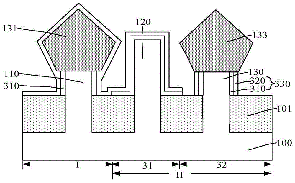
结合参考图3和图4,图3为俯视图(仅示意出衬底和鳍部),图4是图3沿BB1割线的剖面图,提供基底,所述基底包括衬底100以及位于所述衬底100上分立的鳍部(未标示),所述衬底100包括相邻的上拉晶体管区I(如图4所示)和下拉晶体管区II(如图4所示)。3 and 4, FIG. 3 is a top view (only the substrate and the fins are illustrated), and FIG. 4 is a cross-sectional view of FIG. 3 along the secant line BB1, providing a base, the base including the
所述基底为后续形成半导体结构提供工艺平台。本实施例中,所述基底为后续形成SRAM(静态随机随机存储器)提供工艺平台,且所形成SRAM为鳍式场效应管结构,所述上拉晶体管区I为PMOS区域,所述下拉晶体管区II为NMOS区域。The substrate provides a process platform for the subsequent formation of the semiconductor structure. In this embodiment, the substrate provides a process platform for the subsequent formation of SRAM (Static Random Access Memory), and the formed SRAM is a fin field effect transistor structure, the pull-up transistor region I is a PMOS region, and the pull-down transistor region II is the NMOS region.
为了提高SRAM单元区的器件电流,所述下拉晶体管区II包括相邻的第一下拉晶体管区31和第二下拉晶体管区32,且所述第一下拉晶体管区31与所述上拉晶体管区I相邻。In order to improve the device current of the SRAM cell region, the pull-down transistor region II includes the adjacent first pull-
所述下拉晶体管区II用于形成下拉晶体管,所述第一下拉晶体管区31用于形成第一下拉晶体管,所述第二下拉晶体管区32用于形成第二下拉晶体管,且所述第一下拉晶体管和第二下拉晶体管构成并联的下拉晶体管。相应的,所述第一下拉晶体管区31和第二下拉晶体管区32均为NMOS区域。因此,本实施例中,所述第一下拉晶体管区31的衬底100上具有鳍部,所述第二下拉晶体管区32的衬底100上也具有鳍部。The pull-down transistor region II is used to form a pull-down transistor, the first pull-
本实施例中,位于所述上拉晶体管区I衬底100上的鳍部为第一鳍部110,位于所述第一下拉晶体管区31衬底100上的鳍部为第二鳍部120,位于所述第二下拉晶体管区32衬底100上的鳍部为第三鳍部130。In this embodiment, the fins located on the
本实施例中,所述衬底100为硅衬底。在其他实施例中,所述衬底的材料还可以为锗、锗化硅、碳化硅、砷化镓或镓化铟,所述衬底还能够为绝缘体上的硅衬底、绝缘体上的锗衬底、玻璃基底或III-V族化合物衬底(例如氮化镓基底或砷化镓衬底等)。In this embodiment, the
所述鳍部的材料与所述衬底100的材料相同。本实施例中,所述鳍部的材料为硅,即所述第一鳍部110、第二鳍部120和第三鳍部130的材料为硅。在其他实施例中,所述鳍部的材料还可以是锗、锗化硅、碳化硅、砷化镓或镓化铟。The material of the fins is the same as the material of the
具体地,形成所述衬底100和鳍部的工艺步骤包括:提供初始衬底;在所述初始衬底表面形成图形化的第一硬掩膜层(图未示);以所述第一硬掩膜层为掩膜刻蚀所述初始衬底,形成衬底100以及凸出于所述衬底100表面的鳍部。Specifically, the process steps of forming the
本实施例中,形成所述衬底100和鳍部后,保留位于所述鳍部顶部的第一硬掩膜层。所述第一硬掩膜层的材料为氮化硅,后续在进行平坦化处理工艺时,所述第一硬掩膜层顶部表面用于定义平坦化处理工艺的停止位置,并起到保护鳍部顶部的作用。In this embodiment, after the
继续参考图4,需要说明的是,提供所述基底后,所述形成方法还包括:在所述鳍部(未标示)露出的衬底100上形成隔离结构101,所述隔离结构101覆盖所述鳍部的部分侧壁,且所述隔离结构101的顶部低于所述鳍部的顶部。Continuing to refer to FIG. 4 , it should be noted that, after the substrate is provided, the forming method further includes: forming an
所述隔离结构101作为半导体结构的隔离结构,用于对相邻器件起到隔离作用。本实施例中,所述隔离结构101的材料为氧化硅。在其他实施例中,所述隔离结构的材料还可以为氮化硅或氮氧化硅。The
具体地,形成所述隔离结构101的步骤包括:在所述鳍部露出的衬底100上填充隔离材料,所述隔离材料顶部高于所述第一硬掩膜层(图未示)顶部;研磨去除高于所述第一硬掩膜层顶部的隔离材料,形成隔离膜;回刻蚀部分厚度的所述隔离膜,暴露出所述鳍部110顶部以及部分侧壁,形成所述隔离结构101;去除所述第一硬掩膜层。Specifically, the step of forming the
需要说明的是,后续步骤包括形成横跨所述鳍部的栅极结构,在所述下拉晶体管区II栅极结构一侧的鳍部内形成第二下拉掺杂区,且所述第二下拉掺杂区采用对所述鳍部进行离子掺杂的非外延层方式形成,也就是说,形成所述第二下拉掺杂区的步骤中,未形成有外延层,而是直接对所述鳍部进行离子掺杂工艺;因此为了使所形成的下拉晶体管的电学性能不受影响,本实施例中,形成所述隔离膜后,回刻蚀部分厚度的所述隔离膜之前,所述形成方法还包括:对所述第二下拉掺杂区所对应的基底进行下拉阈值调节掺杂(VTImplant)处理,所述下拉阈值调节掺杂处理的掺杂离子为N型离子,N型离子可以为P、As或Sb。It should be noted that the subsequent steps include forming a gate structure across the fin, forming a second pull-down doping region in the fin on one side of the gate structure in the pull-down transistor region II, and the second pull-down doping The impurity region is formed by a non-epitaxial layer method in which the fin is ion-doped, that is, in the step of forming the second pull-down doping region, no epitaxial layer is formed, but the fin is directly doped. The ion doping process is performed; therefore, in order to keep the electrical properties of the formed pull-down transistor unaffected, in this embodiment, after the isolation film is formed, before etching back a partial thickness of the isolation film, the formation method also further Including: performing a pull-down threshold adjustment doping (VTImplant) process on the substrate corresponding to the second pull-down doping region, the doping ions of the pull-down threshold adjustment doping treatment are N-type ions, and the N-type ions may be P, As or Sb.
所述下拉阈值调节掺杂处理的参数可以根据工艺需求而定。本实施例中,所述下拉阈值调节掺杂处理的参数包括:注入的离子能量为1KeV至10KeV,注入的离子剂量为1E13atom/cm2至5E14atom/cm2。The parameters of the pull-down threshold adjustment doping treatment may be determined according to process requirements. In this embodiment, the parameters of the pull-down threshold adjustment doping treatment include: the implanted ion energy is 1KeV to 10KeV, and the implanted ion dose is 1E13atom/cm 2 to 5E14atom/cm 2 .
结合参考图5和图6,图5是立体图(未示出第二硬掩膜层),图6是图5沿E1E2割线的剖面图,形成横跨所述鳍部(未标示)的栅极结构102,且所述栅极结构102覆盖部分鳍部顶部表面和侧壁表面。5 and 6, FIG. 5 is a perspective view (the second hard mask layer is not shown), and FIG. 6 is a cross-sectional view of FIG. 5 along the E1E2 secant line, forming a gate across the fins (not labeled) A
本实施例中,所述上拉晶体管区I和下拉晶体管区II的鳍部上均形成有所述栅极结构102。具体的,位于所述上拉晶体管区I的栅极结构102横跨所述第一鳍部110,且覆盖所述第一鳍部110的部分顶部表面和侧壁表面;位于所述第一下拉晶体管区31的栅极结构102横跨所述第二鳍部120,且覆盖所述第二鳍部120的部分顶部表面和侧壁表面;位于所述第二下拉晶体管区32的栅极结构102横跨所述第三鳍部130,且覆盖所述第三鳍部130的部分顶部表面和侧壁表面。In this embodiment, the
本实施例中,采用后形成高k栅介质层后形成栅电极层(high k last metal gatelast)的工艺,因此所述栅极结构102为伪栅结构(dummy gate),所述栅极结构102为后续所形成半导体结构的实际栅极结构占据空间位置。In this embodiment, a process of forming a high-k gate dielectric layer and then forming a gate electrode layer (high k last metal gate last) is adopted, so the
所述栅极结构102为单层结构或叠层结构。所述栅极结构102包括伪栅层;或者所述栅极结构102包括伪氧化层以及位于所述伪氧化层上的伪栅层。其中,所述伪栅层的材料为多晶硅、氧化硅、氮化硅、氮氧化硅、碳化硅、碳氮化硅、碳氮氧化硅或非晶碳,所述伪氧化层的材料为氧化硅或氮氧化硅。The
具体地,形成所述栅极结构102的步骤包括:在所述隔离结构101上形成伪栅膜,所述伪栅膜横跨所述鳍部,且覆盖鳍部顶部表面和侧壁表面;在所述伪栅膜表面形成第二硬掩膜层200,所述第二硬掩膜层200定义出待形成的栅极结构102的图形;以所述第二硬掩膜层200为掩膜,图形化所述伪栅膜,在所述上拉晶体管区I和下拉晶体管区II的隔离结构101上形成栅极结构102。Specifically, the step of forming the
在其他实施例中,所述栅极结构还能够为后续所形成鳍式场效应管的实际栅极结构,所述栅极结构包括栅介质层以及位于栅介质层表面的栅电极层,其中,所述栅介质层的材料为氧化硅或高k栅介质材料,所述栅电极层的材料为多晶硅或金属材料,所述金属材料包括Ti、Ta、TiN、TaN、TiAl、TiAlN、Cu、Al、W、Ag或Au中的一种或多种。In other embodiments, the gate structure can also be an actual gate structure of a fin field effect transistor formed subsequently, and the gate structure includes a gate dielectric layer and a gate electrode layer located on the surface of the gate dielectric layer, wherein, The material of the gate dielectric layer is silicon oxide or high-k gate dielectric material, the material of the gate electrode layer is polysilicon or metal material, and the metal material includes Ti, Ta, TiN, TaN, TiAl, TiAlN, Cu, Al One or more of , W, Ag or Au.
需要说明的是,本实施例中,形成所述栅极结构102后,保留位于所述栅极结构102顶部上的第二硬掩膜层200。所述第二硬掩膜层200的材料为氮化硅,所述第二硬掩膜层200在后续工艺过程中用于对所述栅极结构102顶部起到保护作用。在其他实施例中,所述第二硬掩膜层的材料还可以为氮氧化硅、碳化硅或氮化硼。It should be noted that, in this embodiment, after the
后续步骤还包括:在所述上拉晶体管区I栅极结构102两侧的第一鳍部110内形成上拉掺杂外延层;在所述第一下拉晶体管区31栅极结构102一侧(如图5中区域C1所示)的第二鳍部120内形成第一下拉掺杂区,且所述第一下拉掺杂区用于与相邻上拉掺杂外延层相连;在所述第一下拉晶体管区31栅极结构102另一侧(如图5中区域C2所示)的第二鳍部120内形成第二下拉掺杂区;在所述第二下拉晶体管区32栅极结构102两侧的第三鳍部130内形成第三下拉掺杂区。Subsequent steps further include: forming a pull-up doped epitaxial layer in the
需要说明的是,随着集成电路特征尺寸持续减小,沿垂直于鳍部延伸方向上,所述第一鳍部110和第二鳍部120之间的距离也相应减小,因此为了避免所述第二下拉掺杂区与相邻所述上拉掺杂外延层发生桥接(bridge)现象,后续形成所述第二下拉掺杂区的步骤中,采用对所述鳍部进行离子掺杂的非外延层方式形成,相比采用选择性外延的工艺,本实施例所述方式可以减小所述第二下拉掺杂区与相邻所述上拉掺杂外延层发生桥接的风险。It should be noted that as the feature size of the integrated circuit continues to decrease, the distance between the
本实施例中,以先形成所述上拉掺杂外延层作为示例进行详细说明。相应的,形成横跨所述鳍部(未标示)的栅极结构(未标示)后,所述方法还包括:In this embodiment, the above-mentioned pull-up doped epitaxial layer is formed first as an example for detailed description. Correspondingly, after forming the gate structure (not shown) across the fins (not shown), the method further includes:
结合参考图7和图8,图7为图6基础上的剖面结构示意图,图8是沿F1F2(如图5所示)割线的剖面结构示意图,在所述上拉晶体管区I的鳍部(未标示)侧壁和顶部上形成P区掩膜层310。7 and FIG. 8, FIG. 7 is a schematic cross-sectional structure diagram based on FIG. 6, and FIG. 8 is a cross-sectional structure schematic diagram along the secant line F1F2 (as shown in FIG. 5), in the fin of the pull-up transistor region I (Not labeled) P-
具体地,在所述第一鳍部110的侧壁和顶部上形成所述P区掩膜层310。Specifically, the P-
本实施例中,所述P区掩膜层310还位于所述第二鳍部120顶部和侧壁上、第三鳍部130顶部和侧壁上,所述P区掩膜层310还位于上拉晶体管区I的栅极结构102顶部和侧壁、下拉晶体管区II的栅极结构102顶部和侧壁上,且还位于所述隔离结构101上。形成所述P区掩膜层310的工艺可以为化学气相沉积工艺、物理气相沉积工艺或原子层沉积工艺。本实施例中,采用原子层沉积工艺形成所述P区掩膜层310。In this embodiment, the P-
所述P区掩膜层310的作用包括:所述P区掩膜层310对所述鳍部侧壁起到保护的作用,避免后续形成上拉掺杂外延层时,在所述第一鳍部110、第二鳍部120和第三鳍部130的侧壁上进行外延生长工艺;此外,位于所述下拉晶体管区II的P区掩膜层310后续还作为下拉晶体管区II的N区掩膜层的一部分。The functions of the P-
所述P区掩膜层310的材料可以为氮化硅、氧化硅、氮化硼或氮氧化硅。所述P区掩膜层310的材料与所述鳍部的材料不同,所述P区掩膜层310的材料与所述隔离结构101的材料也不相同。本实施例中,所述P区掩膜层310的材料为氮化硅。The material of the P-
如无特别说明,后续工艺过程中提供的剖面结构示意图均为在图8基础上的示意图。Unless otherwise specified, the schematic cross-sectional structure diagrams provided in the subsequent process are all schematic diagrams based on FIG. 8 .
参考图9,刻蚀位于所述上拉晶体管区I栅极结构102(如图5所示)两侧鳍部(未标示)顶部上的P区掩膜层310,暴露出所述上拉晶体管区I栅极结构102两侧的鳍部顶部表面,且还刻蚀所述上拉晶体管区I部分厚度的鳍部,在所述上拉晶体管区I的鳍部内形成P区凹槽111。Referring to FIG. 9, the P-
具体地,刻蚀位于所述上拉晶体管区I栅极结构102两侧第一鳍部110顶部上的P区掩膜层310,且还刻蚀部分厚度的第一鳍部110,在所述第一鳍部110内形成所述P区凹槽111。Specifically, the P-
所述P区凹槽111为后续形成上拉掺杂外延层提供空间位置。The P-
需要说明的是,在刻蚀位于所述上拉晶体管区I栅极结构102两侧第一鳍部110顶部上的P区掩膜层310之前,还在所述下拉晶体管区II上形成第一图形层210,所述第一图形层210覆盖所述下拉晶体管区II的P区掩膜层310。所述第一图形层210起到保护所述下拉晶体管区II上P区掩膜层310的作用,所述第一图形层210还可以覆盖所述上拉晶体管区I中不期望被刻蚀的区域。It should be noted that before etching the P-
本实施例中,所述第一图形层210的材料为光刻胶材料。在形成所述P区凹槽111之后,采用湿法去胶或灰化工艺去除所述第一图形层210。In this embodiment, the material of the
具体地,采用干法刻蚀工艺去除位于所述上拉晶体管区I栅极结构102两侧第一鳍部110顶部上的P区掩膜层310;其中,在刻蚀位于所述上拉晶体管区I栅极结构102两侧第一鳍部110顶部上P区掩膜层310的工艺过程中,还刻蚀位于上拉晶体管区I栅极结构102顶部上以及部分隔离结构101上的P区掩膜层310;在所述上拉晶体管区I栅极结构102两侧的第一鳍部110顶部被暴露出来后,继续刻蚀所暴露出的部分厚度的所述第一鳍部110,以形成所述P区凹槽111。Specifically, a dry etching process is used to remove the P
需要说明的是,后续步骤还包括在所述P区凹槽111内形成上拉掺杂外延层;所述上拉掺杂外延层用于向上拉晶体管沟道区提供压应力,以提高上拉晶体管的载流子迁移率,且增大所述上拉掺杂外延层的体积有利于提高载流子迁移率;此外,增大所述上拉掺杂外延层的体积还有利于降低后续所形成金属硅化物与所述上拉掺杂外延层的接触电阻。It should be noted that the subsequent steps further include forming a pull-up doped epitaxial layer in the P-
因此本实施例中,为了增加后续在所述P区凹槽111内所形成上拉掺杂外延层的体积,在刻蚀所述第一鳍部110的同时,还刻蚀位于所述第一鳍部110侧壁上的P区掩膜层310,使得形成P区凹槽111后,位于所述第一鳍部110侧壁上的P区掩膜层310与所述第一鳍部110顶部齐平。Therefore, in this embodiment, in order to increase the volume of the pull-up doped epitaxial layer formed in the P-
还需要说明的是,形成所述P区凹槽111后,所述形成方法还包括:对所述P区凹槽111进行清洗工艺。所述清洗工艺既用于去除所述P区凹槽111表面的杂质,还用于去除位于所述第一鳍部110表面的氧化层(图未示),为后续在所述P区凹槽111内形成上拉掺杂外延层提供良好的界面态。It should also be noted that, after forming the P-
所述清洗工艺采用的清洗溶液可以是氨水、双氧水和水的混合溶液(SC1溶液)以及稀释氢氟酸(DHF)的组合,也可以是臭氧水、SC1溶液和DHF的组合。The cleaning solution used in the cleaning process can be a combination of ammonia water, a mixed solution of hydrogen peroxide and water (SC1 solution) and diluted hydrofluoric acid (DHF), or a combination of ozone water, SC1 solution and DHF.
参考图10,在所述上拉晶体管区I栅极结构102两侧的鳍部(未标示)内形成上拉掺杂外延层131。Referring to FIG. 10 , a pull-up doped
本实施例中,所述上拉晶体管区I为PMOS区域,因此所述上拉掺杂外延层131的掺杂离子为P型离子。In this embodiment, the pull-up transistor region I is a PMOS region, so the doping ions of the pull-up doped
本实施例中,形成所述上拉掺杂外延层131的工艺为原位掺杂的选择性外延工艺。形成所述上拉掺杂外延层131的步骤包括:在所述上拉晶体管区I栅极结构102两侧的第一鳍部110内形成上拉外延层(图未示),且在形成所述上拉外延层的工艺过程中原位自掺杂P型离子,以形成所述上拉掺杂外延层131。In this embodiment, the process of forming the pull-up doped
具体地,在所述P区凹槽111(如图9所示)内形成上拉外延层,且在形成所述上拉外延层的工艺过程中原位自掺杂P型离子,以形成所述上拉掺杂外延层131。Specifically, a pull-up epitaxial layer is formed in the P-region groove 111 (as shown in FIG. 9 ), and P-type ions are self-doped in-situ during the process of forming the pull-up epitaxial layer to form the pull-up epitaxial layer. The doped
所述上拉掺杂外延层131的材料为P型掺杂的Si或SiGe。本实施例中,所述上拉外延层的材料为Si,所述P型离子为Ge离子,因此所述上拉掺杂外延层131为掺杂有Ge离子的Si,即所述上拉掺杂外延层131的材料为SiGe。The material of the pull-up doped
所述上拉掺杂外延层131的Ge离子浓度可以根据工艺需求而定。本实施例中,所述上拉掺杂外延层131的Ge离子浓度为5.02E21atom/cm3至2.5E22atom/cm3。The Ge ion concentration of the pull-up doped
在其他实施例中,还可以在所述P区凹槽内形成上拉外延层后,对所述上拉外延层进行P型离子掺杂形成上拉掺杂外延层。In other embodiments, after the pull-up epitaxial layer is formed in the P region groove, the pull-up epitaxial layer may be doped with P-type ions to form a pull-up doped epitaxial layer.
所述上拉外延层为上拉晶体管区I的沟道区提供压应力作用,从而提高下拉晶体管的载流子迁移率。The pull-up epitaxial layer provides compressive stress to the channel region of the pull-up transistor region I, thereby improving the carrier mobility of the pull-down transistor.
需要说明的是,本实施例中,所述上拉掺杂外延层131的顶部高于所述P区凹槽111的顶部,且由于选择性外延工艺的特性,高于所述P区凹槽111的上拉掺杂外延层131侧壁表面具有向远离所述第一鳍部110方向突出的顶角。在其他实施例中,所述上拉掺杂外延层顶部还可以与所述P区凹槽顶部齐平。It should be noted that, in this embodiment, the top of the pull-up doped
还需要说明的是,所述上拉掺杂外延层131的体积较大,因此所述上拉掺杂外延层131用于提高下拉晶体管载流子迁移率的效果较好;且所述上拉掺杂外延层131的顶部表面面积相应也较大,从而使得后续在所述上拉掺杂外延层131上形成金属硅化物后,所述金属硅化物与所述上拉掺杂外延层131的接触电阻较小。It should also be noted that the volume of the pull-up doped
此外,为了避免后续工艺对所述上拉掺杂外延层131表面造成工艺损伤,形成所述上拉掺杂外延层131后,所述方法还包括:对所述上拉掺杂外延层131表面进行氧化处理,在所述上拉掺杂外延层131表面形成氧化保护层(图未示),所述氧化处理可以为干氧氧化、湿氧氧化或水汽氧化。In addition, in order to avoid process damage to the surface of the pull-up doped
结合参考图11,形成所述上拉掺杂外延层131后,所述形成方法还包括:在所述下拉晶体管区II鳍部(未标示)的顶部和侧壁上形成N区掩膜层330。11 , after forming the pull-up doped
具体的,形成所述N区掩膜层330的步骤包括:在形成所述上拉掺杂外延层131之后,在所述下拉晶体管区II的P区掩膜层310上形成N区掩膜侧墙320,其中,位于所述下拉晶体管区II的P区掩膜层310和所述N区掩膜侧墙320作为所述N区掩膜层330。Specifically, the step of forming the N-
本实施例中,所述N区掩膜层330还位于所述下拉晶体管区II的栅极结构102顶部和侧壁上,且还位于所述下拉晶体管区II的隔离结构101上。In this embodiment, the N-
为了降低工艺难度、节约光罩,本实施例中,所述N区掩膜侧墙320还位于所述上拉掺杂外延层131上以及所述上拉晶体管区I的栅极结构102顶部和侧壁上,且还位于所述上拉晶体管区I的隔离结构101上。In order to reduce the difficulty of the process and save the mask, in this embodiment, the
有关所述N区掩膜侧墙320的材料和形成工艺可参考前述P区掩膜层310的相关描述,在此不再赘述。For the material and formation process of the N-
所述N区掩膜侧墙320的作用包括:由所述N区掩膜侧墙320与所述P区掩膜层310构成叠层结构的N区掩膜层330,后续在所述下拉晶体管区II栅极结构120两侧的鳍部内形成下拉掺杂区时,以所述N区掩膜层330作为掩膜,因此通过所述N区掩膜侧墙320,可以增加后续所形成下拉掺杂区与所述下拉晶体管区II沟道区的距离,有利于改善短沟道效应。The function of the N-
参考图12,刻蚀位于所述下拉晶体管区II栅极结构102一侧(如图5中区域C1所示)鳍部(未标示)顶部上的N区掩膜层330,暴露出所述下拉晶体管区II栅极结构102一侧的鳍部顶部表面,且还刻蚀所述下拉晶体管区II部分厚度的鳍部,在所述下拉晶体管区II栅极结构102一侧的鳍部内形成N区凹槽121。Referring to FIG. 12 , the N-
由于为了避免后续所形成第二下拉掺杂区与相邻所述上拉掺杂外延层131发生桥接现象,后续采用离子掺杂的非外延层方式形成所述第二下拉掺杂区,因此本实施例中,形成所述N区凹槽121的步骤中,仅在所述第一下拉晶体管区31栅极结构102一侧的第二鳍部120内形成所述N区凹槽121。In order to avoid the bridging phenomenon between the subsequently formed second pull-down doped region and the adjacent pull-up doped
本实施例中,所述形成方法还包括:刻蚀位于所述第二下拉晶体管区32栅极结构102两侧第三鳍部130顶部上的N区掩膜层330,暴露出所述第二下拉晶体管区32栅极结构102两侧的第三鳍部130顶部表面,且还刻蚀部分厚度的第三鳍部130,在所述第二下拉晶体管区32栅极结构102两侧的第三鳍部130内形成N区凹槽121。In this embodiment, the forming method further includes: etching the N-
本实施例中,为了简化工艺步骤,节省光罩成本,在同一步骤中,在所述第一下拉晶体管区31栅极结构102一侧的第二鳍部120内、以及所述第二下拉晶体管区32栅极结构102两侧的第三鳍部130内形成所述N区凹槽121。In this embodiment, in order to simplify the process steps and save the cost of the mask, in the same step, in the
所述第二鳍部120内的N区凹槽121为后续在所述第一下拉晶体管区31栅极结构102一侧的第二鳍部120内形成第一下拉掺杂区提供空间位置,所述第三鳍部130内的N区凹槽121为后续在所述第二下拉晶体管区32栅极结构102两侧的第三鳍部130内形成第三下拉掺杂区提供空间位置。The N-
需要说明的是,在刻蚀所述N区掩膜层330之前,在所述上拉晶体管区I和第一下拉晶体管区31栅极结构102另一侧(如图5中区域C2所示)的第二鳍部120上形成第二图形层220,所述第二图形层220还覆盖所述上拉晶体管区I的栅极结构102、下拉晶体管区II的栅极结构102以及隔离结构101。It should be noted that, before the N
具体地,所述第二图形层220形成于所述上拉晶体管区I和第一下拉晶体管区31栅极结构102另一侧的N区掩膜侧墙320上,所述第二图形层220用于保护所述下拉晶体管区II中不期望被刻蚀的区域。Specifically, the
本实施例中,所述第二图形层220的材料为光刻胶材料。在形成所述N区凹槽121之后,采用湿法去胶或灰化工艺去除所述第二图形层220。In this embodiment, the material of the
具体地,采用干法刻蚀工艺,去除位于所述第一下拉晶体管区31栅极结构102一侧第二鳍部120顶部上、以及所述第二下拉晶体管区32栅极结构102两侧第三鳍部130顶部上的N区掩膜层330;其中,在刻蚀所述N区掩膜层330的工艺过程中,还刻蚀位于所述第一下拉晶体管区31栅极结构102顶部上、第二下拉晶体管区32栅极结构102顶部上以及部分隔离结构101上的N区掩膜层330;在所述第一下拉晶体管区31栅极结构102一侧的第二鳍部120顶部、以及第二下拉晶体管区32栅极结构102两侧的第三鳍部130顶部被暴露出来后,继续刻蚀暴露出的所述第二鳍部120和第三鳍部130,以形成所述N区凹槽121。Specifically, a dry etching process is used to remove the top of the
需要说明的是,后续步骤还包括在所述第一下拉掺杂区和第三下拉掺杂区上形成金属硅化物,其中所述金属硅化物与所述第一下拉掺杂区、第三下拉掺杂区的接触电阻与所述第一下拉掺杂区、第三下拉掺杂区的顶部表面面积成反比,增大所述第一下拉掺杂区和第三下拉掺杂区的体积还有利于降低所述接触电阻。It should be noted that the subsequent steps further include forming a metal silicide on the first pull-down doping region and the third pull-down doping region, wherein the metal silicide is connected to the first pull-down doping region and the third pull-down doping region. The contact resistance of the three pull-down doped regions is inversely proportional to the top surface area of the first pull-down doped region and the third pull-down doped region, increasing the first pull-down doped region and the third pull-down doped region The volume is also beneficial to reduce the contact resistance.
因此本实施例中,为了增加后续在所述N区凹槽121内所形成第一下拉掺杂区和第三下拉掺杂区的体积,在刻蚀所述第二鳍部120和第三鳍部130的同时,还刻蚀位于所述第二鳍部120侧壁上的N区掩膜层330以及第三鳍部130侧壁上的N区掩膜层330,使得形成N区凹槽121后,位于所述第二鳍部120侧壁上的N区掩膜层330与所述第二鳍部120顶部齐平,位于所述第三鳍部130侧壁上的N区掩膜层330与所述第三鳍部130顶部齐平。Therefore, in this embodiment, in order to increase the volume of the first pull-down doping region and the third pull-down doping region formed in the
还需要说明的是,形成所述N区凹槽121后,所述形成方法还包括:对所述N区凹槽121进行清洗工艺。所述清洗工艺既用于去除所述N区凹槽121表面的杂质,还用于去除位于所述第二鳍部120和第三鳍部130表面的氧化层(图未示),为后续在所述N区凹槽121内形成第一下拉掺杂区和第三下拉掺杂区提供良好的界面态。It should also be noted that, after forming the N-
所述清洗工艺采用的清洗溶液可以是氨水、双氧水和水的混合溶液(SC1溶液)以及稀释氢氟酸(DHF)的组合,也可以是臭氧水、SC1溶液和DHF的组合。The cleaning solution used in the cleaning process can be a combination of ammonia water, a mixed solution of hydrogen peroxide and water (SC1 solution) and diluted hydrofluoric acid (DHF), or a combination of ozone water, SC1 solution and DHF.
结合参考图13和图14,图13为立体图(未示出P区掩膜层和N区掩膜层),图14是图13沿G1G2割线的剖面图,在所述下拉晶体管区II栅极结构一侧(如图5中区域C1所示)的鳍部内形成第一下拉掺杂区132(如图13所示),所述第一下拉掺杂区132用于与相邻上拉掺杂外延层131相连。13 and 14, FIG. 13 is a perspective view (the P-region mask layer and N-region mask layer are not shown), and FIG. 14 is a cross-sectional view of FIG. 13 along the G1G2 secant line, in the pull-down transistor region II gate A first pull-down doped region 132 (as shown in FIG. 13 ) is formed in the fin on one side of the pole structure (as shown in the region C1 in FIG. 5 ), and the first pull-down doped
具体地,在所述第一下拉晶体管区31的N区凹槽121(如图12所示)内形成所述第一下拉掺杂区132。本实施例中,所述下拉晶体管区II为NMOS区域,因此所述第一下拉掺杂区132的掺杂离子为N型离子。Specifically, the first pull-down doped
需要说明的是,所述N区凹槽121还形成于所述第二下拉晶体管区32栅极结构102两侧的第三鳍部130内,因此形成所述第一下拉掺杂区132的步骤中,还在所述第二下拉晶体管区32的N区凹槽121内形成第三下拉掺杂区133,所述第三下拉掺杂区133的材料与所述第一下拉掺杂区132的材料相同。It should be noted that the N-
形成所述第一下拉掺杂区132和第三下拉掺杂区133的工艺为原位掺杂的选择性外延工艺。具体地,形成所述第一下拉掺杂区132和第三下拉掺杂区133的步骤包括:在所述N区凹槽121内形成下拉外延层(图未示),且在形成所述下拉外延层的工艺过程中原位自掺杂N型离子,以形成所述第一下拉掺杂区132和第三下拉掺杂区133。The process of forming the first pull-down doped
所述第一下拉掺杂区132的材料为N型掺杂的Si或SiC。本实施例中,所述下拉外延层的材料为Si,所述N型离子为P离子,因此所述第一下拉掺杂区132为掺杂有P离子的Si,即所述第一下拉掺杂区132的材料为SiP,相应的,所述第三下拉掺杂区133的材料也为SiP。The material of the first pull-down doped
所述第一下拉掺杂区132的P离子浓度根据实际工艺需求而定。本实施例中,所述第一下拉掺杂区132的P离子浓度为1E20atom/cm3至2E21atom/cm3。相应的,所述第三下拉掺杂区133的P离子浓度为1E20atom/cm3至2E21atom/cm3。The P ion concentration of the first pull-
在其他实施例中,还可以在所述N区凹槽内形成下拉外延层后,对所述下拉外延层进行N型离子掺杂形成所述第一下拉掺杂区和第三下拉掺杂区。In other embodiments, after a pull-down epitaxial layer is formed in the N-region recess, N-type ion doping may be performed on the pull-down epitaxial layer to form the first pull-down doping region and the third pull-down doping region Area.
需要说明的是,本实施例中,所述下拉外延层的顶部高于所述N区凹槽121的顶部,且由于选择性外延工艺的特性,高于所述第一下拉晶体管区31N区凹槽121的下拉外延层侧壁表面具有向远离所述第二鳍部120方向突出的顶角,高于所述第二下拉晶体管区32N区凹槽121的下拉外延层侧壁表面具有向远离所述第三鳍部130方向突出的顶角。在其他实施例中,所述下拉外延层顶部还可以与所述N区凹槽顶部齐平。It should be noted that, in this embodiment, the top of the pull-down epitaxial layer is higher than the top of the N-
还需要说明的是,所述下拉外延层的体积较大,因此所述第一下拉掺杂区132和第三下拉掺杂区133的顶部表面面积相应也较大,从而使得后续在所述第一下拉掺杂区132、第三下拉掺杂区133上形成金属硅化物后,所述金属硅化物与所述第一下拉掺杂区132、第三下拉掺杂区133的接触电阻较小。It should also be noted that the volume of the pull-down epitaxial layer is relatively large, so the top surface areas of the first pull-
结合参考图15和图16,图15是基于图13的立体图(未示出P区掩膜层和N区掩膜层),图16是图15沿I1I2割线的剖面图,在所述下拉晶体管区II栅极结构102另一侧(如图5中区域C2所示)的鳍部(未标示)内形成第二下拉掺杂区(如图15中区域H所示),且所述第二下拉掺杂区采用对所述鳍部进行离子掺杂125的非外延层方式形成。15 and 16, FIG. 15 is a perspective view based on FIG. 13 (the P-region mask layer and N-region mask layer are not shown), and FIG. 16 is a cross-sectional view of FIG. 15 along the I1I2 secant line. A second pull-down doped region (shown as region H in The two pull-down doped regions are formed by means of a non-epitaxial layer in which the fins are ion-doped 125 .
为了避免所述第二下拉掺杂区与相邻所述上拉掺杂外延层131发生桥接现象,本实施例中,所述第二下拉掺杂区采用对所述鳍部进行离子掺杂125的非外延层方式形成,也就是说,所述下拉晶体管区II栅极结构102另一侧的鳍部内未形成有外延层(EPI),而是直接对所述鳍部进行离子掺杂125。In order to avoid the bridging phenomenon between the second pull-down doped region and the adjacent pull-up doped
本实施例中,所述下拉晶体管区II为NMOS区域,因此所述第二下拉掺杂区的掺杂离子为N型离子。具体地,形成所述第二下拉掺杂区的步骤包括:对所述下拉晶体管区I栅极结构102另一侧(如图5中区域C2所示)的鳍部进行N型离子注入工艺。In this embodiment, the pull-down transistor region II is an NMOS region, so the doping ions of the second pull-down doping region are N-type ions. Specifically, the step of forming the second pull-down doped region includes: performing an N-type ion implantation process on the fin on the other side of the
需要说明的是,本实施例中,由于所述第一下拉晶体管区31与所述上拉晶体管区I相邻,因此形成所述第二下拉掺杂区的步骤中,对所述第一下拉晶体管区31栅极结构102另一侧的第二鳍部120进行N型离子注入工艺,在所述第一下拉晶体管区31栅极结构102另一侧的第二鳍部120内形成所述第二下拉掺杂区。It should be noted that, in this embodiment, since the first pull-
具体地,形成覆盖所述上拉晶体管区I和第一下拉掺杂区132的第三图形层230,所述第三图形层230暴露出所述第一下拉晶体管区31栅极结构102另一侧第二鳍部120顶部上的N区掩膜层330;以所述第三图形层为掩膜,对所述N区掩膜层330进行离子掺杂工艺125,在所述第一下拉晶体管区31栅极结构102另一侧的第二鳍部120内形成第二下拉掺杂区。Specifically, a
所述掺杂离子透过所述N区掩膜层330注入至所述第二鳍部120内,从而在所述第一下拉晶体管区31栅极结构102另一侧的第二鳍部120内形成所述第二下拉掺杂区。The dopant ions are implanted into the
由于本实施例中,仅所述第二下拉掺杂区采用离子掺杂的非外延层方式形成,因此所述第三图形层还覆盖所述第二下拉晶体管区32。Since in this embodiment, only the second pull-down doped region is formed by ion-doped non-epitaxial layer, the third pattern layer also covers the second pull-
所述N型离子注入工艺所注入的离子为P离子或As离子。所述N型离子注入工艺的参数根据实际工艺需求而定。本实施例中,所述N型离子注入工艺的步骤包括:注入的离子为P离子,注入的离子能量为1KeV至4KeV,注入的离子剂量为1E15atom/cm2至2E15atom/cm2;或者,注入的离子为As离子,注入的离子能量为1KeV至4KeV,注入的离子剂量为1E15atom/cm2至4E15atom/cm2。The ions implanted in the N-type ion implantation process are P ions or As ions. The parameters of the N-type ion implantation process are determined according to actual process requirements. In this embodiment, the steps of the N-type ion implantation process include: the implanted ions are P ions, the implanted ion energy is 1KeV to 4KeV, and the implanted ion dose is 1E15atom/cm 2 to 2E15atom/cm 2 ; or, implanted The ions are As ions, the implanted ion energy is 1KeV to 4KeV, and the implanted ion dose is 1E15atom/cm 2 to 4E15atom/cm 2 .
本实施例中,在下拉晶体管区栅极结构另一侧的鳍部内形成第二下拉掺杂区,且所述第二下拉掺杂区采用对所述鳍部进行离子掺杂的非外延层方式形成,也就是说,所述下拉晶体管区栅极结构另一侧的鳍部内未形成下拉外延层;由于所述下拉晶体管区与上拉晶体管区相邻,因此相比通过在下拉晶体管区栅极结构另一侧的鳍部内形成下拉外延层以形成第二下拉掺杂区的方案,本发明可以避免因所述下拉晶体管区鳍部和上拉晶体管区鳍部之间距离过近的原因,而出现所述第二下拉掺杂区与所述上拉掺杂外延层发生桥接的问题。In this embodiment, a second pull-down doped region is formed in the fin on the other side of the gate structure of the pull-down transistor region, and the second pull-down doped region adopts a non-epitaxial layer method in which the fin is ion-doped That is to say, the pull-down epitaxial layer is not formed in the fin on the other side of the gate structure of the pull-down transistor region; since the pull-down transistor region is adjacent to the pull-up transistor region, compared with the pull-down transistor region gate In the solution of forming a pull-down epitaxial layer in the fin on the other side of the structure to form the second pull-down doping region, the present invention can avoid the reason that the distance between the pull-down transistor region fin and the pull-up transistor region fin is too close, and The problem of bridging between the second pull-down doped region and the pull-up doped epitaxial layer occurs.
相应的,本发明还提供一种半导体结构。结合参考图17至图19,示出了本发明半导体结构一实施例的结构示意图,其中图17是俯视图(仅示意出衬底和鳍部),图18是图17中区域K的立体图,图19是图18沿L1L2割线的剖面图,所述半导体结构包括:Correspondingly, the present invention also provides a semiconductor structure. Referring to FIGS. 17 to 19 , a schematic structural diagram of an embodiment of the semiconductor structure of the present invention is shown, wherein FIG. 17 is a top view (only the substrate and fins are shown), and FIG. 18 is a perspective view of the region K in FIG. 17 . 19 is a cross-sectional view of FIG. 18 along the L1L2 secant line, the semiconductor structure includes:
基底,包括衬底400以及位于所述衬底400上分立的鳍部(未标示),所述衬底400包括相邻的上拉晶体管区I和下拉晶体管区II;a base, including a
横跨所述鳍部的栅极结构402(如图18所示),且所述栅极结构402覆盖部分鳍部顶部表面和侧壁表面;a
上拉掺杂外延层431,位于所述上拉晶体管区I栅极结构402两侧的鳍部内;The pull-up doped
第一下拉掺杂区432,位于所述下拉晶体管区II栅极结构402一侧的鳍部内,所述第一下拉掺杂区432用于与相邻上拉掺杂外延层431相连;The first pull-down doped
第二下拉掺杂区(如图18中区域J所示),位于所述下拉晶体管区II栅极结构402另一侧的鳍部内,且所述第二下拉掺杂区为非外延层掺杂区。The second pull-down doped region (shown as region J in FIG. 18 ) is located in the fin on the other side of the
本实施例中,所述基底上的半导体结构为SRAM(静态随机随机存储器),且所述SRAM器件为鳍式场效应管,所述上拉晶体管区I为PMOS区域,所述下拉晶体管区II为NMOS区域。In this embodiment, the semiconductor structure on the substrate is an SRAM (Static Random Access Memory), and the SRAM device is a fin field effect transistor, the pull-up transistor region I is a PMOS region, and the pull-down transistor region II for the NMOS region.
为了提高SRAM单元区的器件电流,所述下拉晶体管区II包括相邻的第一下拉晶体管区31和第二下拉晶体管区32,且所述第一下拉晶体管区31与所述上拉晶体管区I相邻。In order to improve the device current of the SRAM cell region, the pull-down transistor region II includes the adjacent first pull-
位于所述第一下拉晶体管区31上的晶体管为第一下拉晶体管,位于所述第二下拉晶体管区32上的晶体管为第二下拉晶体管,所述第一下拉晶体管和第二下拉晶体管构成并联的下拉晶体管。相应的,所述第一下拉晶体管区31和第二下拉晶体管区32均为NMOS区域。因此,所述第一下拉晶体管区31的衬底400上具有鳍部,所述第二下拉晶体管区32的衬底400上也具有鳍部。The transistor on the first pull-
本实施例中,位于所述上拉晶体管区I衬底400上的鳍部为第一鳍部410,位于所述第一下拉晶体管区31衬底400上的鳍部为第二鳍部420,位于所述第二下拉晶体管区32衬底400上的鳍部为第三鳍部430。In this embodiment, the fins located on the
本实施例中,所述衬底400为硅衬底。在其他实施例中,所述衬底的材料还可以为锗、锗化硅、碳化硅、砷化镓或镓化铟,所述衬底还能够为绝缘体上的硅衬底、绝缘体上的锗衬底、玻璃基底或III-V族化合物衬底(例如氮化镓基底或砷化镓衬底等)。In this embodiment, the
所述鳍部的材料与所述衬底400的材料相同。本实施例中,所述鳍部的材料为硅,即所述第一鳍部410、第二鳍部420和第三鳍部430的材料为硅。在其他实施例中,所述鳍部的材料还可以是锗、锗化硅、碳化硅、砷化镓或镓化铟。The material of the fins is the same as the material of the
需要说明的是,所述半导体结构还包括:位于相邻所述鳍部之间衬底400上的隔离结构401,所述隔离结构401覆盖所述鳍部的部分侧壁,且所述隔离结构401的顶部低于所述鳍部的顶部。It should be noted that the semiconductor structure further includes: an
所述隔离结构401作为半导体结构的隔离结构,用于对相邻器件起到隔离作用。本实施例中,所述隔离结构401的材料为氧化硅。在其他实施例中,所述隔离结构的材料还可以为氮化硅或氮氧化硅。The
本实施例中,所述上拉晶体管区I和下拉晶体管区II的鳍部上均具有所述栅极结构402。具体的,位于所述上拉晶体管区I的栅极结构402横跨所述第一鳍部410,且覆盖所述第一鳍部410的部分顶部表面和侧壁表面;位于所述第一下拉晶体管区31的栅极结构402横跨所述第二鳍部420,且覆盖所述第二鳍部420的部分顶部表面和侧壁表面;位于所述第二下拉晶体管区32的栅极结构402横跨所述第三鳍部430,且覆盖所述第三鳍部430的部分顶部表面和侧壁表面。In this embodiment, the
所述栅极结构402包括栅介质层以及位于栅介质层表面的栅电极层,其中,所述栅介质层的材料为氧化硅或高k栅介质材料,所述栅电极层的材料为多晶硅或金属材料,所述金属材料包括Ti、Ta、TiN、TaN、TiAl、TiAlN、Cu、Al、W、Ag或Au中的一种或多种。The
本实施例中,所述上拉晶体管区I为PMOS区域,因此所述上拉掺杂外延层431内具有P型离子。In this embodiment, the pull-up transistor region I is a PMOS region, so the pull-up doped
所述上拉掺杂外延层431的材料为P型掺杂的Si或SiGe。本实施例中,所述上拉掺杂外延层431内的P型离子为Ge离子,所述上拉掺杂外延层431的材料为SiGe。The material of the pull-up doped
所述上拉掺杂外延层431的Ge离子浓度根据实际工艺需求而定。本实施例中,所述上拉掺杂外延层431的Ge离子浓度为5.02E21atom/cm3至2.5E22atom/cm3。The Ge ion concentration of the pull-up doped
需要说明的是,所述上拉掺杂外延层431的体积较大,因此所述上拉掺杂外延层431用于提高下拉晶体管的载流子迁移率的效果较好;且所述上拉掺杂外延层431的顶部表面面积相应也较大,从而使位于所述上拉掺杂外延层431上的金属硅化物与所述上拉掺杂外延层431的接触电阻较小。It should be noted that the volume of the pull-up doped
本实施例中,所述下拉晶体管区II包括相邻的第一下拉晶体管区31和第二下拉晶体管区32,且所述第一下拉晶体管区31与所述上拉晶体管区I相邻,因此所述第一下拉掺杂区432位于所述第一下拉晶体管区31栅极结构402一侧的第二鳍部120内,所述第二下拉掺杂区(如图18中区域J所示)位于所述第一下拉晶体管区31栅极结构402另一侧的第二鳍部120内。In this embodiment, the pull-down transistor region II includes an adjacent first pull-
本实施例中,所述下拉晶体管区II为NMOS区域,因此所述第一下拉掺杂区432和第二下拉掺杂区内均具有N型离子。In this embodiment, the pull-down transistor region II is an NMOS region, so both the first pull-
需要说明的是,所述第一下拉掺杂区432用于与相邻所述上拉掺杂外延层431相连,因此本实施例中,仅所述第二下拉掺杂区为非外延层掺杂区,也就是说,仅所述第二下拉掺杂区所对应的第二鳍部420内不具有下拉外延层,从而可以避免因相邻鳍部之间距离过近或外延层体积过大的原因,而出现所述第二下拉掺杂区与相邻所述上拉掺杂外延层431发生桥接(bridge)的现象。It should be noted that the first pull-down doped
所述第二下拉掺杂区的掺杂离子为P离子或As离子。所述第二下拉掺杂区的离子浓度根据实际工艺需求而定。本实施例中,所述第二下拉掺杂区的掺杂离子为P离子,所述第二下拉掺杂区的P离子浓度为1E19atom/cm3至1E21atom/cm3;或者,所述第二下拉掺杂区的掺杂离子为As离子,所述第二下拉掺杂区的P离子浓度为1E21atom/cm3至1E22atom/cm3。The doping ions of the second pull-down doping region are P ions or As ions. The ion concentration of the second pull-down doping region is determined according to actual process requirements. In this embodiment, the doping ions of the second pull-down doping region are P ions, and the P ion concentration of the second pull-down doping region is 1E19 atom/cm 3 to 1E21 atom/cm 3 ; or, the second The doping ions of the pull-down doping region are As ions, and the P ion concentration of the second pull-down doping region is 1E21 atom/cm 3 to 1E22 atom/cm 3 .
还需要说明的是,为了使位于所述第一下拉掺杂区432上的金属硅化物与所述第一下拉掺杂区432的接触电阻较小,本实施例中,所述第一下拉掺杂区432所对应的鳍部内具有下拉外延层(图未示),所述第一下拉掺杂区432位于所述下拉外延层内,所述下拉外延层的材料为Si或SiC。It should also be noted that, in order to make the contact resistance between the metal silicide located on the first pull-
相应的,所述第一下拉掺杂区432的材料为N型掺杂的Si或SiC。本实施例中,所述第一下拉掺杂区432的材料为SiP。Correspondingly, the material of the first pull-down doped
所述第一下拉掺杂区432的离子浓度根据实际工艺需求而定。本实施例中,所述第一下拉掺杂区432的P离子浓度为1E20atom/cm3至2E21atom/cm3。The ion concentration of the first pull-down doped
所述第一下拉掺杂区432的体积较大,因此所述第一下拉掺杂区432的顶部表面面积相应也较大,从而使位于所述第一下拉掺杂区432上的金属硅化物与所述第一下拉掺杂区432的接触电阻较小。The volume of the first pull-down doped
本实施例中,所述下拉晶体管区II还包括第二下拉晶体管区32,因此,所述半导体结构还包括:第三下拉掺杂区433,位于所述第二下拉晶体管区32栅极结构402两侧的第三鳍部130内,所述第三下拉掺杂区433的材料与所述第一下拉掺杂区432的材料相同。相应的,所述第三下拉掺杂区433的材料为SiP,所述第三下拉掺杂区433的P离子浓度为1E20atom/cm3至2E21atom/cm3。In this embodiment, the pull-down transistor region II further includes a second pull-
本实施例中,所述半导体结构包括第二下拉掺杂区,所述第二下拉掺杂区位于所述下拉晶体管区栅极结构另一侧鳍部内,且所述第二下拉掺杂区为非外延层掺杂区,也就是说,所述下拉晶体管区栅极结构另一侧的鳍部内不具有下拉外延层;由于所述下拉晶体管区与上拉晶体管区相邻,因此相比所述下拉晶体管区栅极结构另一侧鳍部内具有下拉外延层的方案,本发明所述半导体结构可以避免因所述下拉晶体管区鳍部和上拉晶体管区鳍部之间距离过近的原因,而出现所述第二下拉掺杂区与所述上拉掺杂外延层发生桥接的问题。In this embodiment, the semiconductor structure includes a second pull-down doped region, the second pull-down doped region is located in the fin on the other side of the gate structure of the pull-down transistor region, and the second pull-down doped region is Non-epitaxial layer doped region, that is, the fin on the other side of the gate structure of the pull-down transistor region does not have a pull-down epitaxial layer; since the pull-down transistor region is adjacent to the pull-up transistor region, compared with the pull-down transistor region In the solution of having a pull-down epitaxial layer in the fin on the other side of the gate structure of the pull-down transistor region, the semiconductor structure of the present invention can avoid the reason that the distance between the fin of the pull-down transistor region and the fin of the pull-up transistor region is too close, and The problem of bridging between the second pull-down doped region and the pull-up doped epitaxial layer occurs.
继续参考图17至图19,相应的,本发明还提供一种SRAM(静态随机随机存储器),所述SRAM包括前述实施例所述的半导体结构。Continuing to refer to FIGS. 17 to 19 , correspondingly, the present invention further provides an SRAM (Static Random Access Memory), where the SRAM includes the semiconductor structure described in the foregoing embodiments.
对所述半导体结构的具体描述请参考前述实施例中半导体结构的相应描述,在此不再赘述。For the specific description of the semiconductor structure, please refer to the corresponding description of the semiconductor structure in the foregoing embodiments, which will not be repeated here.
由于所述SRAM中,位于所述下拉晶体管区栅极结构另一侧鳍部内的第二下拉掺杂区为非外延层掺杂区,也就是说,所述下拉晶体管区栅极结构另一侧鳍部内不具有下拉外延层;由于所述下拉晶体管区与上拉晶体管区相邻,因此相比所述下拉晶体管区栅极结构另一侧鳍部内具有下拉外延层的方案,本发明所述半导体结构可以避免因所述下拉晶体管区鳍部和上拉晶体管区鳍部之间距离过近的原因,而出现所述第二下拉掺杂区与所述上拉掺杂外延层发生桥接的问题。Because in the SRAM, the second pull-down doped region located in the fin on the other side of the pull-down transistor region gate structure is a non-epitaxial layer doped region, that is, the other side of the pull-down transistor region gate structure The fin does not have a pull-down epitaxial layer; since the pull-down transistor region is adjacent to the pull-up transistor region, compared with the solution in which the pull-down transistor region has a pull-down epitaxial layer on the other side of the gate structure of the pull-down transistor region, the semiconductor of the present invention The structure can avoid the problem of bridging between the second pull-down doped region and the pull-up doped epitaxial layer because the distance between the pull-down transistor region fin and the pull-up transistor region fin is too close.
虽然本发明披露如上,但本发明并非限定于此。任何本领域技术人员,在不脱离本发明的精神和范围内,均可作各种更动与修改,因此本发明的保护范围应当以权利要求所限定的范围为准。Although the present invention is disclosed above, the present invention is not limited thereto. Any person skilled in the art can make various changes and modifications without departing from the spirit and scope of the present invention. Therefore, the protection scope of the present invention should be based on the scope defined by the claims.
Claims (12)
Priority Applications (4)
| Application Number | Priority Date | Filing Date | Title |
|---|---|---|---|
| CN201611072328.XA CN108122976B (en) | 2016-11-29 | 2016-11-29 | Semiconductor structure, forming method thereof and SRAM |
| EP17203763.2A EP3327788B1 (en) | 2016-11-29 | 2017-11-27 | Semiconductor structure, static random access memory, and fabrication method thereof |
| US15/824,830 US10256243B2 (en) | 2016-11-29 | 2017-11-28 | Semiconductor structure, static random access memory, and fabrication method thereof |
| US16/277,254 US20190181146A1 (en) | 2016-11-29 | 2019-02-15 | Semiconductor structure and static random access memory |
Applications Claiming Priority (1)
| Application Number | Priority Date | Filing Date | Title |
|---|---|---|---|
| CN201611072328.XA CN108122976B (en) | 2016-11-29 | 2016-11-29 | Semiconductor structure, forming method thereof and SRAM |
Publications (2)
| Publication Number | Publication Date |
|---|---|
| CN108122976A CN108122976A (en) | 2018-06-05 |
| CN108122976B true CN108122976B (en) | 2020-11-03 |
Family
ID=60480213
Family Applications (1)
| Application Number | Title | Priority Date | Filing Date |
|---|---|---|---|
| CN201611072328.XA Active CN108122976B (en) | 2016-11-29 | 2016-11-29 | Semiconductor structure, forming method thereof and SRAM |
Country Status (3)
| Country | Link |
|---|---|
| US (2) | US10256243B2 (en) |
| EP (1) | EP3327788B1 (en) |
| CN (1) | CN108122976B (en) |
Families Citing this family (10)
| Publication number | Priority date | Publication date | Assignee | Title |
|---|---|---|---|---|
| CN108122976B (en) * | 2016-11-29 | 2020-11-03 | 中芯国际集成电路制造(上海)有限公司 | Semiconductor structure, forming method thereof and SRAM |
| US10483267B2 (en) | 2017-06-30 | 2019-11-19 | Taiwan Semiconductor Manufacturing Co., Ltd. | Eight-transistor static random-access memory, layout thereof, and method for manufacturing the same |
| US10510894B2 (en) * | 2017-11-30 | 2019-12-17 | Taiwan Semiconductor Manufacturing Co., Ltd. | Isolation structure having different distances to adjacent FinFET devices |
| CN110581133B (en) * | 2018-06-08 | 2022-09-13 | 中芯国际集成电路制造(上海)有限公司 | Semiconductor structure, forming method thereof and SRAM |
| KR102655419B1 (en) | 2019-05-14 | 2024-04-05 | 삼성전자주식회사 | Semiconductor devices |
| CN112151452B (en) * | 2019-06-28 | 2024-03-26 | 中芯国际集成电路制造(上海)有限公司 | Semiconductor structures and methods of forming them |
| CN110289243B (en) * | 2019-07-17 | 2021-08-10 | 上海华力集成电路制造有限公司 | Method for manufacturing semiconductor device |
| US12237414B2 (en) * | 2021-05-07 | 2025-02-25 | Taiwan Semicondcutor Manufacturing Co., Ltd. | Source/drain features with improved strain properties |
| CN113611743B (en) | 2021-06-11 | 2022-06-07 | 联芯集成电路制造(厦门)有限公司 | Semiconductor transistor structure and manufacturing method thereof |
| KR20230033029A (en) | 2021-08-25 | 2023-03-08 | 삼성전자주식회사 | Semiconductor device and method for manufacturing the same |
Family Cites Families (48)
| Publication number | Priority date | Publication date | Assignee | Title |
|---|---|---|---|---|
| US7449373B2 (en) * | 2006-03-31 | 2008-11-11 | Intel Corporation | Method of ion implanting for tri-gate devices |
| US8624295B2 (en) * | 2008-03-20 | 2014-01-07 | Taiwan Semiconductor Manufacturing Company, Ltd. | SRAM devices utilizing strained-channel transistors and methods of manufacture |
| US8283231B2 (en) * | 2008-06-11 | 2012-10-09 | Taiwan Semiconductor Manufacturing Company, Ltd. | finFET drive strength modification |
| US9245805B2 (en) * | 2009-09-24 | 2016-01-26 | Taiwan Semiconductor Manufacturing Company, Ltd. | Germanium FinFETs with metal gates and stressors |
| US8557692B2 (en) * | 2010-01-12 | 2013-10-15 | Taiwan Semiconductor Manufacturing Company, Ltd. | FinFET LDD and source drain implant technique |
| US8399931B2 (en) * | 2010-06-30 | 2013-03-19 | Taiwan Semiconductor Manufacturing Company, Ltd. | Layout for multiple-fin SRAM cell |
| KR101776926B1 (en) * | 2010-09-07 | 2017-09-08 | 삼성전자주식회사 | Semiconductor device and method for manufacturing the same |
| US8431455B2 (en) * | 2011-06-27 | 2013-04-30 | Globalfoundries Inc. | Method of improving memory cell device by ion implantation |
| US9048261B2 (en) * | 2011-08-04 | 2015-06-02 | International Business Machines Corporation | Fabrication of field-effect transistors with atomic layer doping |
| US8772874B2 (en) * | 2011-08-24 | 2014-07-08 | International Business Machines Corporation | MOSFET including asymmetric source and drain regions |
| US9040399B2 (en) * | 2011-10-27 | 2015-05-26 | International Business Machines Corporation | Threshold voltage adjustment for thin body MOSFETs |
| US8987831B2 (en) * | 2012-01-12 | 2015-03-24 | Taiwan Semiconductor Manufacturing Company, Ltd. | SRAM cells and arrays |
| US8637371B2 (en) * | 2012-02-16 | 2014-01-28 | International Business Machines Corporation | Non-planar MOSFET structures with asymmetric recessed source drains and methods for making the same |
| US9036404B2 (en) * | 2012-03-30 | 2015-05-19 | Taiwan Semiconductor Manufacturing Company, Ltd. | Methods and apparatus for SRAM cell structure |
| KR102049774B1 (en) * | 2013-01-24 | 2019-11-28 | 삼성전자 주식회사 | Semiconductor device and fabricated method thereof |
| KR102018101B1 (en) * | 2013-02-04 | 2019-11-14 | 삼성전자 주식회사 | Semiconductor device and method for fabricating the same |
| KR102068980B1 (en) * | 2013-08-01 | 2020-01-22 | 삼성전자 주식회사 | Semiconductor device and method for fabricating the same |
| US9006805B2 (en) * | 2013-08-07 | 2015-04-14 | United Microelectronics Corp. | Semiconductor device |
| US9761594B2 (en) * | 2013-10-02 | 2017-09-12 | Globalfoundries Inc. | Hardmask for a halo/extension implant of a static random access memory (SRAM) layout |
| KR102158962B1 (en) * | 2014-05-08 | 2020-09-24 | 삼성전자 주식회사 | Semiconductor device and method for fabricating the same |
| KR102158961B1 (en) * | 2014-05-13 | 2020-09-24 | 삼성전자 주식회사 | Semiconductor device and method for fabricating the same |
| KR102160100B1 (en) * | 2014-05-27 | 2020-09-25 | 삼성전자 주식회사 | Method for fabricating semiconductor device |
| US9893183B2 (en) * | 2014-07-10 | 2018-02-13 | Taiwan Semiconductor Manufacturing Company Ltd. | Semiconductor structure and manufacturing method thereof |
| US9418728B2 (en) * | 2014-07-24 | 2016-08-16 | Taiwan Semiconductor Manufacturing Company, Ltd. | Dual-port static random-access memory cell |
| KR102227128B1 (en) * | 2014-09-03 | 2021-03-12 | 삼성전자주식회사 | Semiconductor device and method for fabricating the same |
| US9793356B2 (en) * | 2014-09-12 | 2017-10-17 | Samsung Electronics Co., Ltd. | Semiconductor device and method for fabricating the same |
| CN105514160B (en) * | 2014-09-26 | 2019-05-07 | 中芯国际集成电路制造(上海)有限公司 | LDMOS device and method of making the same |
| US9324623B1 (en) * | 2014-11-26 | 2016-04-26 | Samsung Electronics Co., Ltd. | Method of manufacturing semiconductor device having active fins |
| CN106206692B (en) * | 2015-04-30 | 2019-09-27 | 中芯国际集成电路制造(上海)有限公司 | Forming method of N-type fin field effect transistor |
| KR102374108B1 (en) * | 2015-06-02 | 2022-03-14 | 삼성전자주식회사 | Semiconductor device having stressor and method of fabricating the same |
| KR102427326B1 (en) * | 2015-10-26 | 2022-08-01 | 삼성전자주식회사 | Semiconductor device and method for manufacturing the same |
| US9768178B2 (en) * | 2015-11-11 | 2017-09-19 | Taiwan Semiconductor Manufacturing Co., Ltd. | Semiconductor device, static random access memory cell and manufacturing method of semiconductor device |
| CN106920776B (en) * | 2015-12-25 | 2019-12-03 | 中芯国际集成电路制造(上海)有限公司 | Method of forming a fin transistor |
| US9935199B2 (en) * | 2016-01-15 | 2018-04-03 | Taiwan Semiconductor Manufacturing Company, Ltd. | FinFET with source/drain structure |
| US10050043B2 (en) * | 2016-01-29 | 2018-08-14 | Taiwan Semiconductor Manufacturing Co., Ltd. | Static random access memory (SRAM) using FinFETs with varying widths of fin structures |
| US9601497B1 (en) * | 2016-04-28 | 2017-03-21 | Taiwan Semiconductor Manufacturing Co., Ltd. | Static random access memory and method of manufacturing the same |
| CN107346762A (en) * | 2016-05-05 | 2017-11-14 | 中芯国际集成电路制造(上海)有限公司 | The forming method of fin field effect pipe |
| KR102486477B1 (en) * | 2016-05-31 | 2023-01-06 | 삼성전자주식회사 | Semiconductor device and method for fabricating the same |
| CN107452627B (en) * | 2016-06-01 | 2020-12-18 | 中芯国际集成电路制造(上海)有限公司 | Manufacturing method of semiconductor device |
| KR102592326B1 (en) * | 2016-06-20 | 2023-10-20 | 삼성전자주식회사 | Integrated circuit device and method of manufacturing the same |
| US9640540B1 (en) * | 2016-07-19 | 2017-05-02 | Taiwan Semiconductor Manufacturing Co., Ltd. | Structure and method for an SRAM circuit |
| CN107919327B (en) * | 2016-10-10 | 2020-09-08 | 中芯国际集成电路制造(上海)有限公司 | Semiconductor structure and method of forming the same |
| CN107958873B (en) * | 2016-10-18 | 2020-11-27 | 中芯国际集成电路制造(上海)有限公司 | Fin-type field effect transistor and method of forming the same |
| US10727234B2 (en) * | 2016-11-27 | 2020-07-28 | United Microelectronics Corp. | Layout of semiconductor transistor device |
| CN108122973B (en) * | 2016-11-28 | 2020-06-09 | 中芯国际集成电路制造(上海)有限公司 | Semiconductor structure and method of forming the same, and SRAM |
| CN108122976B (en) * | 2016-11-29 | 2020-11-03 | 中芯国际集成电路制造(上海)有限公司 | Semiconductor structure, forming method thereof and SRAM |
| US10886268B2 (en) * | 2016-11-29 | 2021-01-05 | Taiwan Semiconductor Manufacturing Co., Ltd. | Method of manufacturing a semiconductor device with separated merged source/drain structure |
| US9991165B1 (en) * | 2016-11-29 | 2018-06-05 | Taiwan Semiconductor Manufacturing Company, Ltd. | Asymmetric source/drain epitaxy |
-
2016
- 2016-11-29 CN CN201611072328.XA patent/CN108122976B/en active Active
-
2017
- 2017-11-27 EP EP17203763.2A patent/EP3327788B1/en active Active
- 2017-11-28 US US15/824,830 patent/US10256243B2/en active Active
-
2019
- 2019-02-15 US US16/277,254 patent/US20190181146A1/en not_active Abandoned
Also Published As
| Publication number | Publication date |
|---|---|
| US20190181146A1 (en) | 2019-06-13 |
| EP3327788B1 (en) | 2021-08-04 |
| US20180151574A1 (en) | 2018-05-31 |
| CN108122976A (en) | 2018-06-05 |
| US10256243B2 (en) | 2019-04-09 |
| EP3327788A1 (en) | 2018-05-30 |
Similar Documents
| Publication | Publication Date | Title |
|---|---|---|
| CN108122976B (en) | Semiconductor structure, forming method thereof and SRAM | |
| US10741453B2 (en) | FinFET device | |
| US10541238B2 (en) | FinFET and fabrication method thereof | |
| CN110265301B (en) | Semiconductor structure and forming method thereof | |
| CN104517901B (en) | The forming method of CMOS transistor | |
| US20180047829A1 (en) | Semiconductor structure and fabrication method thereof | |
| CN106952810B (en) | Manufacturing method of semiconductor structure | |
| CN106952806A (en) | Improve the method for fin field effect pipe performance | |
| CN108122973B (en) | Semiconductor structure and method of forming the same, and SRAM | |
| CN111613581B (en) | Semiconductor structure and forming method thereof | |
| CN108010846B (en) | Method and semiconductor structure for improving short channel effect | |
| CN109003899B (en) | Semiconductor structure and method for forming the same, and method for forming a fin field effect transistor | |
| CN111463275A (en) | Semiconductor structure and method of forming the same | |
| CN110707010B (en) | Semiconductor structures and methods of forming them | |
| CN109087892B (en) | Semiconductor structure, forming method thereof and forming method of fin field effect transistor | |
| CN112151452A (en) | Semiconductor structure and method of forming the same | |
| CN111435645B (en) | Semiconductor structures and methods of forming them | |
| CN112652578B (en) | Method of forming semiconductor structure, transistor | |
| CN109427679B (en) | Semiconductor structure and method of forming the same | |
| CN104143530B (en) | Transistor and preparation method thereof | |
| CN111697052B (en) | Semiconductor structure and forming method thereof | |
| CN110875185B (en) | Semiconductor structures and methods of forming them | |
| CN107437533A (en) | Semiconductor structure and its manufacture method | |
| CN107492496B (en) | Semiconductor structure and manufacturing method thereof | |
| CN106486370A (en) | The forming method of semiconductor devices |
Legal Events
| Date | Code | Title | Description |
|---|---|---|---|
| PB01 | Publication | ||
| PB01 | Publication | ||
| SE01 | Entry into force of request for substantive examination | ||
| SE01 | Entry into force of request for substantive examination | ||
| GR01 | Patent grant | ||
| GR01 | Patent grant |