CN113611743B - Semiconductor transistor structure and manufacturing method thereof - Google Patents
Semiconductor transistor structure and manufacturing method thereof Download PDFInfo
- Publication number
- CN113611743B CN113611743B CN202110651874.3A CN202110651874A CN113611743B CN 113611743 B CN113611743 B CN 113611743B CN 202110651874 A CN202110651874 A CN 202110651874A CN 113611743 B CN113611743 B CN 113611743B
- Authority
- CN
- China
- Prior art keywords
- layer
- epitaxial layer
- conductivity type
- epitaxial
- fin structure
- Prior art date
- Legal status (The legal status is an assumption and is not a legal conclusion. Google has not performed a legal analysis and makes no representation as to the accuracy of the status listed.)
- Active
Links
- 239000004065 semiconductor Substances 0.000 title claims abstract description 31
- 238000004519 manufacturing process Methods 0.000 title abstract description 5
- 239000000758 substrate Substances 0.000 claims abstract description 27
- 229910000577 Silicon-germanium Inorganic materials 0.000 claims description 32
- 229910052732 germanium Inorganic materials 0.000 claims description 16
- GNPVGFCGXDBREM-UHFFFAOYSA-N germanium atom Chemical compound [Ge] GNPVGFCGXDBREM-UHFFFAOYSA-N 0.000 claims description 16
- 238000000034 method Methods 0.000 claims description 16
- OAICVXFJPJFONN-UHFFFAOYSA-N Phosphorus Chemical compound [P] OAICVXFJPJFONN-UHFFFAOYSA-N 0.000 claims description 10
- 229910052785 arsenic Inorganic materials 0.000 claims description 10
- RQNWIZPPADIBDY-UHFFFAOYSA-N arsenic atom Chemical compound [As] RQNWIZPPADIBDY-UHFFFAOYSA-N 0.000 claims description 10
- 229910052698 phosphorus Inorganic materials 0.000 claims description 10
- 239000011574 phosphorus Substances 0.000 claims description 10
- XUIMIQQOPSSXEZ-UHFFFAOYSA-N Silicon Chemical group [Si] XUIMIQQOPSSXEZ-UHFFFAOYSA-N 0.000 claims description 9
- 229910052710 silicon Inorganic materials 0.000 claims description 9
- 239000010703 silicon Substances 0.000 claims description 9
- BHEPBYXIRTUNPN-UHFFFAOYSA-N hydridophosphorus(.) (triplet) Chemical compound [PH] BHEPBYXIRTUNPN-UHFFFAOYSA-N 0.000 claims 2
- VYPSYNLAJGMNEJ-UHFFFAOYSA-N Silicium dioxide Chemical compound O=[Si]=O VYPSYNLAJGMNEJ-UHFFFAOYSA-N 0.000 description 5
- 229910052814 silicon oxide Inorganic materials 0.000 description 5
- ZOXJGFHDIHLPTG-UHFFFAOYSA-N Boron Chemical compound [B] ZOXJGFHDIHLPTG-UHFFFAOYSA-N 0.000 description 4
- 229910052796 boron Inorganic materials 0.000 description 4
- 238000010586 diagram Methods 0.000 description 4
- 229910052581 Si3N4 Inorganic materials 0.000 description 3
- 229910021420 polycrystalline silicon Inorganic materials 0.000 description 3
- 229920005591 polysilicon Polymers 0.000 description 3
- HQVNEWCFYHHQES-UHFFFAOYSA-N silicon nitride Chemical compound N12[Si]34N5[Si]62N3[Si]51N64 HQVNEWCFYHHQES-UHFFFAOYSA-N 0.000 description 3
- 238000005530 etching Methods 0.000 description 2
- 230000005669 field effect Effects 0.000 description 2
- 238000009413 insulation Methods 0.000 description 2
- 125000006850 spacer group Chemical group 0.000 description 2
- 230000007812 deficiency Effects 0.000 description 1
- 238000005516 engineering process Methods 0.000 description 1
- 238000012986 modification Methods 0.000 description 1
- 230000004048 modification Effects 0.000 description 1
- 238000007517 polishing process Methods 0.000 description 1
- 239000000126 substance Substances 0.000 description 1
Images


Classifications
-
- H—ELECTRICITY
- H10—SEMICONDUCTOR DEVICES; ELECTRIC SOLID-STATE DEVICES NOT OTHERWISE PROVIDED FOR
- H10D—INORGANIC ELECTRIC SEMICONDUCTOR DEVICES
- H10D30/00—Field-effect transistors [FET]
- H10D30/60—Insulated-gate field-effect transistors [IGFET]
- H10D30/62—Fin field-effect transistors [FinFET]
- H10D30/6215—Fin field-effect transistors [FinFET] having multiple independently-addressable gate electrodes
-
- H—ELECTRICITY
- H10—SEMICONDUCTOR DEVICES; ELECTRIC SOLID-STATE DEVICES NOT OTHERWISE PROVIDED FOR
- H10D—INORGANIC ELECTRIC SEMICONDUCTOR DEVICES
- H10D30/00—Field-effect transistors [FET]
- H10D30/60—Insulated-gate field-effect transistors [IGFET]
- H10D30/751—Insulated-gate field-effect transistors [IGFET] having composition variations in the channel regions
-
- H—ELECTRICITY
- H10—SEMICONDUCTOR DEVICES; ELECTRIC SOLID-STATE DEVICES NOT OTHERWISE PROVIDED FOR
- H10D—INORGANIC ELECTRIC SEMICONDUCTOR DEVICES
- H10D30/00—Field-effect transistors [FET]
- H10D30/01—Manufacture or treatment
- H10D30/021—Manufacture or treatment of FETs having insulated gates [IGFET]
- H10D30/024—Manufacture or treatment of FETs having insulated gates [IGFET] of fin field-effect transistors [FinFET]
-
- H—ELECTRICITY
- H10—SEMICONDUCTOR DEVICES; ELECTRIC SOLID-STATE DEVICES NOT OTHERWISE PROVIDED FOR
- H10D—INORGANIC ELECTRIC SEMICONDUCTOR DEVICES
- H10D30/00—Field-effect transistors [FET]
- H10D30/60—Insulated-gate field-effect transistors [IGFET]
- H10D30/62—Fin field-effect transistors [FinFET]
- H10D30/6211—Fin field-effect transistors [FinFET] having fin-shaped semiconductor bodies integral with the bulk semiconductor substrates
-
- H—ELECTRICITY
- H10—SEMICONDUCTOR DEVICES; ELECTRIC SOLID-STATE DEVICES NOT OTHERWISE PROVIDED FOR
- H10D—INORGANIC ELECTRIC SEMICONDUCTOR DEVICES
- H10D30/00—Field-effect transistors [FET]
- H10D30/60—Insulated-gate field-effect transistors [IGFET]
- H10D30/791—Arrangements for exerting mechanical stress on the crystal lattice of the channel regions
- H10D30/797—Arrangements for exerting mechanical stress on the crystal lattice of the channel regions being in source or drain regions, e.g. SiGe source or drain
-
- H—ELECTRICITY
- H10—SEMICONDUCTOR DEVICES; ELECTRIC SOLID-STATE DEVICES NOT OTHERWISE PROVIDED FOR
- H10D—INORGANIC ELECTRIC SEMICONDUCTOR DEVICES
- H10D62/00—Semiconductor bodies, or regions thereof, of devices having potential barriers
- H10D62/10—Shapes, relative sizes or dispositions of the regions of the semiconductor bodies; Shapes of the semiconductor bodies
- H10D62/124—Shapes, relative sizes or dispositions of the regions of semiconductor bodies or of junctions between the regions
-
- H—ELECTRICITY
- H10—SEMICONDUCTOR DEVICES; ELECTRIC SOLID-STATE DEVICES NOT OTHERWISE PROVIDED FOR
- H10D—INORGANIC ELECTRIC SEMICONDUCTOR DEVICES
- H10D62/00—Semiconductor bodies, or regions thereof, of devices having potential barriers
- H10D62/10—Shapes, relative sizes or dispositions of the regions of the semiconductor bodies; Shapes of the semiconductor bodies
- H10D62/17—Semiconductor regions connected to electrodes not carrying current to be rectified, amplified or switched, e.g. channel regions
- H10D62/213—Channel regions of field-effect devices
- H10D62/221—Channel regions of field-effect devices of FETs
- H10D62/235—Channel regions of field-effect devices of FETs of IGFETs
- H10D62/314—Channel regions of field-effect devices of FETs of IGFETs having vertical doping variations
-
- H—ELECTRICITY
- H10—SEMICONDUCTOR DEVICES; ELECTRIC SOLID-STATE DEVICES NOT OTHERWISE PROVIDED FOR
- H10D—INORGANIC ELECTRIC SEMICONDUCTOR DEVICES
- H10D84/00—Integrated devices formed in or on semiconductor substrates that comprise only semiconducting layers, e.g. on Si wafers or on GaAs-on-Si wafers
- H10D84/01—Manufacture or treatment
- H10D84/0123—Integrating together multiple components covered by H10D12/00 or H10D30/00, e.g. integrating multiple IGBTs
- H10D84/0126—Integrating together multiple components covered by H10D12/00 or H10D30/00, e.g. integrating multiple IGBTs the components including insulated gates, e.g. IGFETs
- H10D84/0158—Integrating together multiple components covered by H10D12/00 or H10D30/00, e.g. integrating multiple IGBTs the components including insulated gates, e.g. IGFETs the components including FinFETs
-
- H—ELECTRICITY
- H10—SEMICONDUCTOR DEVICES; ELECTRIC SOLID-STATE DEVICES NOT OTHERWISE PROVIDED FOR
- H10D—INORGANIC ELECTRIC SEMICONDUCTOR DEVICES
- H10D84/00—Integrated devices formed in or on semiconductor substrates that comprise only semiconducting layers, e.g. on Si wafers or on GaAs-on-Si wafers
- H10D84/01—Manufacture or treatment
- H10D84/02—Manufacture or treatment characterised by using material-based technologies
- H10D84/03—Manufacture or treatment characterised by using material-based technologies using Group IV technology, e.g. silicon technology or silicon-carbide [SiC] technology
- H10D84/038—Manufacture or treatment characterised by using material-based technologies using Group IV technology, e.g. silicon technology or silicon-carbide [SiC] technology using silicon technology, e.g. SiGe
-
- H—ELECTRICITY
- H10—SEMICONDUCTOR DEVICES; ELECTRIC SOLID-STATE DEVICES NOT OTHERWISE PROVIDED FOR
- H10D—INORGANIC ELECTRIC SEMICONDUCTOR DEVICES
- H10D62/00—Semiconductor bodies, or regions thereof, of devices having potential barriers
- H10D62/80—Semiconductor bodies, or regions thereof, of devices having potential barriers characterised by the materials
- H10D62/82—Heterojunctions
- H10D62/822—Heterojunctions comprising only Group IV materials heterojunctions, e.g. Si/Ge heterojunctions
Landscapes
- Insulated Gate Type Field-Effect Transistor (AREA)
Abstract
本发明公开一种半导体晶体管结构及其制作方法,其中该半导体晶体管结构,包含一基底,具有一第一导电型;一鳍结构,成长在所述基底上,所述鳍结构包含具有与所述第一导电型相反的第二导电型的一第一外延层、在所述第一外延层上的一第二外延层,以及在所述第二外延层上具有所述第二导电型的一第三外延层;以及一栅极,位于所述鳍结构上。
The present invention discloses a semiconductor transistor structure and a manufacturing method thereof, wherein the semiconductor transistor structure includes a substrate having a first conductivity type; a fin structure grown on the substrate, the fin structure including a first epitaxial layer of a second conductivity type opposite to the first conductivity type, a second epitaxial layer on the first epitaxial layer, and a second epitaxial layer having the second conductivity type on the second epitaxial layer a third epitaxial layer; and a gate on the fin structure.
Description
技术领域technical field
本发明涉及半导体技术领域,特别是涉及一种改良的半导体晶体管结构。The present invention relates to the field of semiconductor technology, in particular to an improved semiconductor transistor structure.
背景技术Background technique
鳍式场效应晶体管(finfet)被制造在从基底向上延伸的薄“鳍”(或鳍结构)上。鳍式场效应晶体管的通道形成在鳍结构中。栅极设置在鳍结构上,通过栅极控制鳍结构中的通道。Fin field effect transistors (finfets) are fabricated on thin "fins" (or fin structures) that extend upward from the substrate. The channel of the fin field effect transistor is formed in the fin structure. The gate is disposed on the fin structure, and the channel in the fin structure is controlled by the gate.
随着集成电路尺寸的微缩,由于晶体管需具有更高的驱动电流,所以不能很好地控制漏电流。As the size of integrated circuits shrinks, the leakage current cannot be well controlled because the transistors need to have higher drive currents.
发明内容SUMMARY OF THE INVENTION
本发明的主要目的在于提供一种改良的半导体晶体管结构,以解决上述现有技术的不足与缺点。The main purpose of the present invention is to provide an improved semiconductor transistor structure to solve the above-mentioned deficiencies and disadvantages of the prior art.
本发明一方面提供一种半导体晶体管结构,包含:一基底,具有一第一导电型;一鳍结构,成长在所述基底上,所述鳍结构包含具有与所述第一导电型相反的第二导电型的一第一外延层、在所述第一外延层上的一第二外延层,以及在所述第二外延层上具有所述第二导电型的一第三外延层;以及一栅极,位于所述鳍结构上。One aspect of the present invention provides a semiconductor transistor structure, comprising: a substrate having a first conductivity type; a fin structure grown on the substrate, the fin structure including a second conductivity type opposite to the first conductivity type A first epitaxial layer of two conductivity types, a second epitaxial layer on the first epitaxial layer, and a third epitaxial layer having the second conductivity type on the second epitaxial layer; and a a gate on the fin structure.
根据本发明实施例,所述第一导电型为P型,所述第二导电型为N型。According to an embodiment of the present invention, the first conductivity type is P-type, and the second conductivity type is N-type.
根据本发明实施例,具有所述第二导电型的所述第一外延层和所述第三外延层包含掺杂磷或砷的SiGe层。According to an embodiment of the present invention, the first epitaxial layer and the third epitaxial layer having the second conductivity type comprise SiGe layers doped with phosphorus or arsenic.
根据本发明实施例,所述磷或砷的浓度在
根据本发明实施例,所述SiGe层的厚度在
根据本发明实施例,所述第二外延层是本征SiGe层。According to an embodiment of the present invention, the second epitaxial layer is an intrinsic SiGe layer.
根据本发明实施例,所述第二外延层是P型掺杂SiGe层。According to an embodiment of the present invention, the second epitaxial layer is a P-type doped SiGe layer.
根据本发明实施例,所述鳍结构具有3nm至100nm的宽度。According to an embodiment of the present invention, the fin structure has a width of 3 nm to 100 nm.
根据本发明实施例,所述半导体晶体管结构另包含一栅极介电层,介于所述栅极和所述鳍结构之间。According to an embodiment of the present invention, the semiconductor transistor structure further includes a gate dielectric layer between the gate and the fin structure.
根据本发明实施例,所述半导体晶体管结构另包含:一缓冲层,设置在所述鳍结构的底部;以及一应变松弛层,设于所述缓冲层上。According to an embodiment of the present invention, the semiconductor transistor structure further includes: a buffer layer disposed on the bottom of the fin structure; and a strain relaxation layer disposed on the buffer layer.
本发明另一方面提供一种形成半导体晶体管结构的方法,包含:提供具有第一导电型的一基底;在所述基底上成长一鳍结构,所述鳍结构包含具有与所述第一导电型相反的第二导电型的一第一外延层、在所述第一外延层上的一第二外延层,以及在所述第二外延层上的具有所述第二导电型的一第三外延层;以及在所述鳍结构上形成一栅极。Another aspect of the present invention provides a method of forming a semiconductor transistor structure, comprising: providing a substrate with a first conductivity type; growing a fin structure on the substrate, the fin structure including a substrate having a conductivity type similar to that of the first conductivity type A first epitaxial layer of the opposite second conductivity type, a second epitaxial layer on the first epitaxial layer, and a third epitaxial layer having the second conductivity type on the second epitaxial layer layer; and forming a gate on the fin structure.
根据本发明实施例,所述第一导电型为P型,所述第二导电型为N型。According to an embodiment of the present invention, the first conductivity type is P-type, and the second conductivity type is N-type.
根据本发明实施例,具有所述第二导电型的所述第一外延层和所述第三外延层包含掺杂磷或砷的SiGe层。According to an embodiment of the present invention, the first epitaxial layer and the third epitaxial layer having the second conductivity type comprise SiGe layers doped with phosphorus or arsenic.
根据本发明实施例,所述磷或砷的浓度在
根据本发明实施例,所述SiGe层的厚度在
根据本发明实施例,所述第二外延层是本征SiGe层。According to an embodiment of the present invention, the second epitaxial layer is an intrinsic SiGe layer.
根据本发明实施例,所述第二外延层是P型掺杂SiGe层。According to an embodiment of the present invention, the second epitaxial layer is a P-type doped SiGe layer.
根据本发明实施例,所述鳍结构具有3nm至100nm的宽度。According to an embodiment of the present invention, the fin structure has a width of 3 nm to 100 nm.
根据本发明实施例,所述方法另包含:在所述栅极和所述鳍结构之间形成一栅极介电层。According to an embodiment of the present invention, the method further includes: forming a gate dielectric layer between the gate and the fin structure.
根据本发明实施例,所述方法另包含:在所述鳍结构的底部形成一缓冲层;以及在所述缓冲层上形成一应变松弛层。According to an embodiment of the present invention, the method further includes: forming a buffer layer on the bottom of the fin structure; and forming a strain relaxation layer on the buffer layer.
附图说明Description of drawings
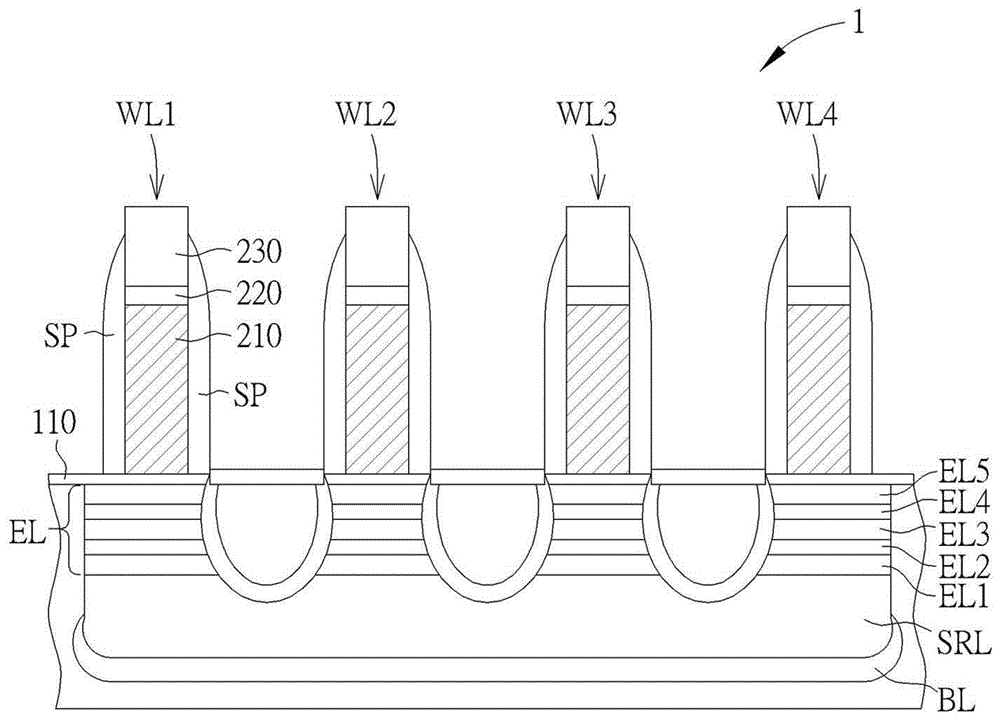
图1为半导体晶体管结构的上视示意图;1 is a schematic top view of a semiconductor transistor structure;
图2为沿着图1中的I-I’切线所示的剖面示意图;Fig. 2 is a cross-sectional schematic diagram shown along the tangent line I-I' in Fig. 1;
图3为沿着图1中的II-II’切线所示的剖面示意图;Fig. 3 is the cross-sectional schematic diagram shown along the II-II' tangent in Fig. 1;
图4至图7为本发明实施例所绘示的半导体晶体管结构的制作方法示意图。4 to 7 are schematic diagrams of a method for fabricating a semiconductor transistor structure according to an embodiment of the present invention.
主要元件符号说明Description of main component symbols
1 半导体晶体管结构1 Semiconductor transistor structure
100 基底100 base
102 沟槽绝缘结构102 Trench Insulation Structure
102s 顶表面102s top surface
110 栅极介电层110 Gate Dielectric Layer
120 绝缘层120 Insulation
210 多晶硅层210 polysilicon layer
220 氮化硅盖层220 Silicon Nitride Cap
230 氧化硅硬掩模层230 Silicon oxide hard mask layer
BL 缓冲层BL buffer
EL 外延层EL epitaxial layer
EL1 第一外延层EL1 first epitaxial layer
EL2 第二外延层EL2 second epitaxial layer
EL3 第三外延层EL3 third epitaxial layer
EL4 第四外延层EL4 fourth epitaxial layer
EL5 第五外延层EL5 fifth epitaxial layer
F1~F3 鳍结构F1~F3 Fin structure
FI1~FI3 鳍结构FI1~FI3 Fin structure
FT1~FT3 鳍沟槽结构FT1~FT3 Fin Trench Structure
R、R1~R3 口袋状凹陷区域R, R1~R3 pocket-shaped recessed area
S1~S3 顶面S1~S3 top surface
SP 间隙壁SP spacers
SRL 应变松弛层SRL strain relaxation layer
T1~T3 沟槽T1~T3 groove
w 宽度w width
WL1~WL4 栅极WL1~WL4 gate
具体实施方式Detailed ways
在下文中,将参照附图说明细节,该些附图中的内容也构成说明书细节描述的一部分,并且以可实行该实施例的特例描述方式来绘示。下文实施例已描述足够的细节使该领域的一般技术人士得以具以实施。In the following, details will be explained with reference to the accompanying drawings, the contents of which also form a part of the detailed description of the specification, and are shown in a description of a specific example in which this embodiment can be carried out. The following examples are described in sufficient detail to enable those of ordinary skill in the art to practice.
当然,也可采行其他的实施例,或是在不悖离文中所述实施例的前提下作出任何结构性、逻辑性、及电性上的改变。因此,下文的细节描述不应被视为是限制,反之,其中所包含的实施例将由随附的权利要求来加以界定。Of course, other embodiments can also be adopted, or any structural, logical, and electrical changes can be made without departing from the embodiments described herein. Therefore, the following detailed description is not to be regarded as limiting, but rather the embodiments contained therein are to be defined by the appended claims.
请参阅图1至图3,其中图1例示半导体晶体管结构的上视示意图,图2为沿着图1中的I-I’切线所示的剖面示意图,图3为沿着图1中的II-II’切线所示的剖面示意图。如图1至图3所示,本发明一种半导体晶体管结构1,例如,PMOS晶体管,包含一基底100,具有一第一导电型,例如,第一导电型可以是P型,基底100可以是P型硅基底。在基底100上例示有三个沿着参考x轴方向延伸的鳍结构F1~F3,以外延方式,成长在基底100上。Please refer to FIGS. 1 to 3 , wherein FIG. 1 is a schematic top view of a semiconductor transistor structure, FIG. 2 is a schematic cross-sectional view taken along the line II' in FIG. 1 , and FIG. 3 is a schematic view taken along the line II in FIG. 1 . - Schematic cross-section shown by the tangent line II'. As shown in FIGS. 1 to 3 , a
根据本发明实施例,基底100另设置有一沟槽绝缘结构102。鳍结构F1~F3则是突出于沟槽绝缘结构102的顶表面102s。根据本发明实施例,各个鳍结构F1~F3的宽度w约为3nm至100nm,但不限于此。According to the embodiment of the present invention, the
根据本发明实施例,各个鳍结构F1~F3包含有交错叠设的外延层EL。根据本发明实施例,外延层EL可以至少包含具有与第一导电型相反的第二导电型的一第一外延层EL1、在第一外延层EL1上的一第二外延层EL2,以及在第二外延层EL2上具有第二导电型的一第三外延层EL3。根据本发明实施例,例如,第一导电型为P型,第二导电型为N型。According to the embodiment of the present invention, each of the fin structures F1 ˜ F3 includes the epitaxial layers EL that are alternately stacked. According to an embodiment of the present invention, the epitaxial layer EL may at least include a first epitaxial layer EL1 having a second conductivity type opposite to the first conductivity type, a second epitaxial layer EL2 on the first epitaxial layer EL1, and a second epitaxial layer EL2 on the first epitaxial layer EL1. There is a third epitaxial layer EL3 of the second conductivity type on the two epitaxial layers EL2. According to an embodiment of the present invention, for example, the first conductivity type is P-type, and the second conductivity type is N-type.
当然,外延层EL的层数不限于三层,也可以是五层或七层。例如,在图2和图3中,还可以在第三外延层EL3上设置第四外延层EL4,并在第四外延层EL4上设置具有第二导电型的第五外延层EL5。Of course, the number of epitaxial layers EL is not limited to three layers, and may be five layers or seven layers. For example, in FIG. 2 and FIG. 3 , the fourth epitaxial layer EL4 may also be provided on the third epitaxial layer EL3, and the fifth epitaxial layer EL5 having the second conductivity type may be provided on the fourth epitaxial layer EL4.
根据本发明实施例,第二外延层EL2和第四外延层EL4可以是本征SiGe(intrinsicSiGe)层(或未掺杂SiGe层),其中,锗浓度可以介于20%至100%之间,可以用来作为让电洞流动的通道层。根据本发明实施例,具有第二导电型的第一外延层EL1、第三外延层EL3和第五外延层EL5包含掺杂磷或砷的SiGe层,如此使得交错叠设的外延层EL具有n-i-n-i-n组态,其可以在MOS晶体管元件的尺寸小于10nm时,还能提高晶体管的操作效能,通过在外延层EL中提供多通道,可以更有效的控制漏电流,并提供较高的驱动电流。According to the embodiment of the present invention, the second epitaxial layer EL2 and the fourth epitaxial layer EL4 may be intrinsic SiGe (intrinsicSiGe) layers (or undoped SiGe layers), wherein the germanium concentration may be between 20% and 100%, Can be used as a channel layer for holes to flow. According to the embodiment of the present invention, the first epitaxial layer EL1, the third epitaxial layer EL3 and the fifth epitaxial layer EL5 having the second conductivity type comprise SiGe layers doped with phosphorus or arsenic, so that the alternately stacked epitaxial layers EL have n-i-n-i-n The configuration can improve the operating efficiency of the transistor when the size of the MOS transistor element is less than 10 nm. By providing multiple channels in the epitaxial layer EL, the leakage current can be more effectively controlled and a higher driving current can be provided.
根据本发明实施例,例如,第一外延层EL1、第三外延层EL3和第五外延层EL5中的磷或砷的浓度可以在


根据本发明另一实施例,第二外延层EL2和第四外延层EL4可以是P型掺杂SiGe层,如此使得交错叠设的外延层EL具有n-p-n-p-n组态。According to another embodiment of the present invention, the second epitaxial layer EL2 and the fourth epitaxial layer EL4 may be P-type doped SiGe layers, so that the alternately stacked epitaxial layers EL have an n-p-n-p-n configuration.
在本发明其他实施例中,半导体晶体管结构1可以是NMOS晶体管,其中,第一外延层EL1、第三外延层EL3和第五外延层EL5可以是掺杂硼的SiC层或Si层(硼的浓度可以在
或者,第一外延层EL1、第三外延层EL3和第五外延层EL5可以是掺杂硼的SiC层或Si层(硼的浓度可以在
根据本发明实施例,半导体晶体管结构1可以另包含一缓冲层BL,设置在各个鳍结构F1~F3的底部。根据本发明实施例,缓冲层BL形成在口袋状凹陷区域R,其中,口袋状凹陷区域R的深度约在30nm至100nm之间,缓冲层BL的厚度约在5nm至35nm之间。According to an embodiment of the present invention, the
根据本发明实施例,口袋状凹陷区域R加上缓冲层BL可以降低后续外延成长外延层EL造成的差排(dislocation)现象,并且使所成长的外延层EL在后续的热制作工艺中具有较高稳定性。根据本发明实施例,缓冲层BL可以是掺杂锗的硅层,且具有渐层或梯度变化的锗浓度,例如,锗浓度可以从0到25%(原子百分比),但不限于此。According to the embodiment of the present invention, the addition of the buffer layer BL to the pocket-shaped recessed region R can reduce the dislocation phenomenon caused by the subsequent epitaxial growth of the epitaxial layer EL, and make the grown epitaxial layer EL have a higher quality in the subsequent thermal fabrication process. High stability. According to an embodiment of the present invention, the buffer layer BL may be a silicon layer doped with germanium, and has a gradient or gradient of germanium concentration, for example, the germanium concentration may be from 0 to 25% (atomic percent), but not limited thereto.
根据本发明实施例,半导体晶体管结构1另包含一应变松弛层SRL,设于缓冲层BL上。根据本发明实施例,应变松弛层SRL介于具有第二导电型的第一外延层EL1和缓冲层BL之间。根据本发明实施例,应变松弛层SRL可以是掺杂锗的硅层,且具有渐层或梯度变化的锗浓度,其中,应变松弛层SRL的锗浓度可以超过25%(原子百分比)。According to an embodiment of the present invention, the
根据本发明实施例,如图1所示,半导体晶体管结构1可以另包含栅极WL1~WL4,位于鳍结构F1~F3上。根据本发明实施例,如图2和图3所示,各个栅极WL1~WL4可以包含多晶硅层210、氮化硅盖层220和氧化硅硬掩模层230,但不限于此。According to an embodiment of the present invention, as shown in FIG. 1 , the
根据本发明实施例,半导体晶体管结构1另包含一栅极介电层110,介于各个栅极WL1~WL4和各个鳍结构F1~F3之间。根据本发明实施例,如图2所示,半导体晶体管结构1可以另包含一间隙壁SP,设置在各个栅极WL1~WL4的侧壁上。According to an embodiment of the present invention, the
请参阅图4至图7,其为根据本发明实施例所绘示的半导体晶体管结构的制作方法示意图。如图4所示,首先提供具有第一导电型的基底100。例如,第一导电型可以是P型,基底100可以是P型硅基底。在基底100上形成有多个鳍结构FI1~FI3。鳍结构FI1~FI3突出于沟槽绝缘结构102,且被绝缘层120包围。根据本发明实施例,例如,绝缘层120可以是氧化硅层。Please refer to FIG. 4 to FIG. 7 , which are schematic diagrams of a method for fabricating a semiconductor transistor structure according to an embodiment of the present invention. As shown in FIG. 4, a
根据本发明实施例,鳍结构FI1~FI3是由基底100的一部分蚀刻出来的,例如,鳍结构FI1~FI3可以只包含硅。经由化学机械研磨制作工艺,可以将绝缘层120的平坦化,使得鳍结构FI1~FI3的顶面S1~S3分别被显露出来。According to an embodiment of the present invention, the fin structures FI1 - FI3 are etched from a part of the
如图5所示,接着进行一蚀刻制作工艺,将鳍结构FI1~FI3去除,在绝缘层120中形成沟槽T1~T3,并且继续蚀刻基底100,在基底100中形成口袋状凹陷区域R1~R3。沟槽T1~T3和口袋状凹陷区域R1~R3分别构成鳍沟槽结构FT1~FT3。As shown in FIG. 5 , an etching process is then performed to remove the fin structures FI1 to FI3 , to form trenches T1 to T3 in the insulating
如图6所示,接着进行外延制作工艺。根据本发明实施例,可以先在鳍沟槽结构FT1~FT3的底部形成缓冲层BL。根据本发明实施例,缓冲层BL形成在口袋状凹陷区域R,其中,口袋状凹陷区域R的深度约在30nm至100nm之间,缓冲层BL的厚度约在5nm至35nm之间。As shown in FIG. 6 , an epitaxial fabrication process is then performed. According to the embodiment of the present invention, the buffer layer BL may be formed at the bottom of the fin trench structures FT1 - FT3 first. According to an embodiment of the present invention, the buffer layer BL is formed in the pocket-shaped recessed region R, wherein the depth of the pocket-shaped recessed region R is about 30 nm to 100 nm, and the thickness of the buffer layer BL is about 5 nm to 35 nm.
根据本发明实施例,口袋状凹陷区域R加上缓冲层BL可以降低后续外延成长外延层EL造成的差排现象,并且使所成长的外延层EL在后续的热制作工艺中具有较高稳定性。根据本发明实施例,缓冲层BL可以是掺杂锗的硅层,且具有渐层或梯度变化的锗浓度,例如,锗浓度可以从0到25%(原子百分比),但不限于此。According to the embodiment of the present invention, adding the buffer layer BL to the pocket-shaped recessed region R can reduce the dislocation phenomenon caused by the subsequent epitaxial growth of the epitaxial layer EL, and make the grown epitaxial layer EL have high stability in the subsequent thermal fabrication process. . According to an embodiment of the present invention, the buffer layer BL may be a silicon layer doped with germanium, and has a gradient or gradient of germanium concentration, for example, the germanium concentration may be from 0 to 25% (atomic percent), but not limited thereto.
根据本发明实施例,接着可以于缓冲层BL上继续形成应变松弛层SRL。根据本发明实施例,应变松弛层SRL可以是掺杂锗的硅层,且具有渐层或梯度变化的锗浓度,其中,应变松弛层SRL的锗浓度可以超过25%(原子百分比)。According to the embodiment of the present invention, the strain relaxation layer SRL may be further formed on the buffer layer BL. According to an embodiment of the present invention, the strain relaxation layer SRL may be a germanium-doped silicon layer with a graded or graded germanium concentration, wherein the germanium concentration of the strain relaxation layer SRL may exceed 25 atomic percent.
根据本发明实施例,接着经由鳍沟槽结构FT1~FT3在应变松弛层SRL上成长出鳍结构F1~F3。根据本发明实施例,各个鳍结构F1~F3包含有交错叠设的外延层EL。根据本发明实施例,外延层EL可以至少包含具有与第一导电型相反的第二导电型的一第一外延层EL1、在第一外延层EL1上的一第二外延层EL2,以及在第二外延层EL2上具有第二导电型的一第三外延层EL3。根据本发明实施例,例如,第一导电型为P型,第二导电型为N型。According to the embodiment of the present invention, the fin structures F1 ˜ F3 are then grown on the strain relaxation layer SRL through the fin trench structures FT1 ˜ FT3 . According to the embodiment of the present invention, each of the fin structures F1 ˜ F3 includes the epitaxial layers EL that are alternately stacked. According to an embodiment of the present invention, the epitaxial layer EL may at least include a first epitaxial layer EL1 having a second conductivity type opposite to the first conductivity type, a second epitaxial layer EL2 on the first epitaxial layer EL1, and a second epitaxial layer EL2 on the first epitaxial layer EL1. There is a third epitaxial layer EL3 of the second conductivity type on the two epitaxial layers EL2. According to an embodiment of the present invention, for example, the first conductivity type is P-type, and the second conductivity type is N-type.
当然,外延层EL的层数不限于三层,也可以是五层或七层。例如,在图2和图3中,还可以在第三外延层EL3上设置第四外延层EL4,并在第四外延层EL4上设置具有第二导电型的第五外延层EL5。Of course, the number of epitaxial layers EL is not limited to three layers, and may be five layers or seven layers. For example, in FIG. 2 and FIG. 3 , the fourth epitaxial layer EL4 may also be provided on the third epitaxial layer EL3, and the fifth epitaxial layer EL5 having the second conductivity type may be provided on the fourth epitaxial layer EL4.
根据本发明实施例,第二外延层EL2和第四外延层EL4可以是本征SiGe层(或未掺杂SiGe层),其中,锗浓度可以介于20%至100%之间,可以用来作为让电洞流动的通道层。根据本发明实施例,具有第二导电型的第一外延层EL1、第三外延层EL3和第五外延层EL5包含掺杂磷或砷的SiGe层,如此使得交错叠设的外延层EL具有n-i-n-i-n组态,其可以在MOS晶体管元件的尺寸小于10nm时,还能提高晶体管的操作效能,通过在外延层EL中提供多通道,可以更有效的控制漏电流,并提供较高的驱动电流。According to an embodiment of the present invention, the second epitaxial layer EL2 and the fourth epitaxial layer EL4 may be intrinsic SiGe layers (or undoped SiGe layers), wherein the germanium concentration may be between 20% and 100%, which may be used for as a channel layer for holes to flow. According to the embodiment of the present invention, the first epitaxial layer EL1, the third epitaxial layer EL3 and the fifth epitaxial layer EL5 having the second conductivity type comprise SiGe layers doped with phosphorus or arsenic, so that the alternately stacked epitaxial layers EL have n-i-n-i-n The configuration can improve the operating efficiency of the transistor when the size of the MOS transistor element is less than 10 nm. By providing multiple channels in the epitaxial layer EL, the leakage current can be more effectively controlled and a higher driving current can be provided.
根据本发明实施例,例如,第一外延层EL1、第三外延层EL3和第五外延层EL5中的磷或砷的浓度可以在

根据本发明另一实施例,第二外延层EL2和第四外延层EL4可以是P型掺杂SiGe层,如此使得交错叠设的外延层EL具有n-p-n-p-n组态。According to another embodiment of the present invention, the second epitaxial layer EL2 and the fourth epitaxial layer EL4 may be P-type doped SiGe layers, so that the alternately stacked epitaxial layers EL have an n-p-n-p-n configuration.
在本发明其他实施例中,半导体晶体管结构1可以是NMOS晶体管,其中,第一外延层EL1、第三外延层EL3和第五外延层EL5可以是掺杂硼的SiC层或Si层(硼的浓度可以在
或者,第一外延层EL1、第三外延层EL3和第五外延层EL5可以是掺杂硼的SiC层或Si层(硼的浓度可以在
如图7所示,接着可以去除绝缘层120,显露出鳍结构F1~F3。然后于鳍结构F1~F3上形成栅极WL3。根据本发明实施例,栅极WL1~WL3可以包含多晶硅层210、氮化硅盖层220和氧化硅硬掩模层230,但不限于此。根据本发明实施例,在栅极WL3和鳍结构F1~F3之间可以形成栅极介电层110,例如,氧化硅层。As shown in FIG. 7 , the insulating
以上所述仅为本发明的优选实施例,凡依本发明权利要求所做的均等变化与修饰,都应属本发明的涵盖范围。The above descriptions are only preferred embodiments of the present invention, and all equivalent changes and modifications made according to the claims of the present invention shall fall within the scope of the present invention.
Claims (13)
Priority Applications (3)
| Application Number | Priority Date | Filing Date | Title |
|---|---|---|---|
| CN202110651874.3A CN113611743B (en) | 2021-06-11 | 2021-06-11 | Semiconductor transistor structure and manufacturing method thereof |
| US17/377,319 US11955536B2 (en) | 2021-06-11 | 2021-07-15 | Semiconductor transistor structure and fabrication method thereof |
| US18/594,006 US20240258406A1 (en) | 2021-06-11 | 2024-03-04 | Semiconductor transistor structure |
Applications Claiming Priority (1)
| Application Number | Priority Date | Filing Date | Title |
|---|---|---|---|
| CN202110651874.3A CN113611743B (en) | 2021-06-11 | 2021-06-11 | Semiconductor transistor structure and manufacturing method thereof |
Publications (2)
| Publication Number | Publication Date |
|---|---|
| CN113611743A CN113611743A (en) | 2021-11-05 |
| CN113611743B true CN113611743B (en) | 2022-06-07 |
Family
ID=78303486
Family Applications (1)
| Application Number | Title | Priority Date | Filing Date |
|---|---|---|---|
| CN202110651874.3A Active CN113611743B (en) | 2021-06-11 | 2021-06-11 | Semiconductor transistor structure and manufacturing method thereof |
Country Status (2)
| Country | Link |
|---|---|
| US (2) | US11955536B2 (en) |
| CN (1) | CN113611743B (en) |
Families Citing this family (1)
| Publication number | Priority date | Publication date | Assignee | Title |
|---|---|---|---|---|
| US11257908B2 (en) * | 2018-10-26 | 2022-02-22 | Taiwan Semiconductor Manufacturing Company, Ltd. | Transistors with stacked semiconductor layers as channels |
Citations (12)
| Publication number | Priority date | Publication date | Assignee | Title |
|---|---|---|---|---|
| JP2006093717A (en) * | 2004-09-25 | 2006-04-06 | Samsung Electronics Co Ltd | Field effect transistor having a deformed channel layer and method for manufacturing the same |
| US9461110B1 (en) * | 2015-04-30 | 2016-10-04 | Taiwan Semiconductor Manufacturing Company, Ltd. | FETs and methods of forming FETs |
| CN106571340A (en) * | 2015-10-07 | 2017-04-19 | 台湾积体电路制造股份有限公司 | Strained nanowire CMOS device and method of forming |
| CN106611787A (en) * | 2015-10-26 | 2017-05-03 | 联华电子股份有限公司 | Semiconductor structure and manufacturing method thereof |
| CN106960846A (en) * | 2016-01-12 | 2017-07-18 | 联华电子股份有限公司 | Semiconductor element and manufacturing method thereof |
| CN107623033A (en) * | 2016-07-13 | 2018-01-23 | 中芯国际集成电路制造(上海)有限公司 | More raceway groove all-around-gate pole devices and its manufacture method |
| US10141430B1 (en) * | 2017-07-27 | 2018-11-27 | Taiwan Semiconductor Manufacturing Co., Ltd. | Fin structures with uniform threshold voltage distribution and method of making the same |
| CN109103108A (en) * | 2018-08-29 | 2018-12-28 | 中国科学院微电子研究所 | A method of forming a semiconductor device |
| CN109427588A (en) * | 2017-08-31 | 2019-03-05 | 台湾积体电路制造股份有限公司 | The method and semiconductor devices of manufacturing semiconductor devices |
| CN110783192A (en) * | 2018-07-31 | 2020-02-11 | 台湾积体电路制造股份有限公司 | Method of manufacturing semiconductor device and semiconductor device |
| CN111162044A (en) * | 2018-11-08 | 2020-05-15 | 中芯国际集成电路制造(上海)有限公司 | Method for manufacturing a semiconductor device, semiconductor device and electronic device |
| CN112242434A (en) * | 2019-07-18 | 2021-01-19 | 台湾积体电路制造股份有限公司 | Method of manufacturing semiconductor device and semiconductor device |
Family Cites Families (23)
| Publication number | Priority date | Publication date | Assignee | Title |
|---|---|---|---|---|
| US6399970B2 (en) * | 1996-09-17 | 2002-06-04 | Matsushita Electric Industrial Co., Ltd. | FET having a Si/SiGeC heterojunction channel |
| US20020100942A1 (en) * | 2000-12-04 | 2002-08-01 | Fitzgerald Eugene A. | CMOS inverter and integrated circuits utilizing strained silicon surface channel MOSFETs |
| KR100487566B1 (en) * | 2003-07-23 | 2005-05-03 | 삼성전자주식회사 | Fin field effect transistors and methods of formiing the same |
| KR100674914B1 (en) * | 2004-09-25 | 2007-01-26 | 삼성전자주식회사 | Morse transistor having a modified channel layer and method of manufacturing same |
| US7713803B2 (en) * | 2007-03-29 | 2010-05-11 | Intel Corporation | Mechanism for forming a remote delta doping layer of a quantum well structure |
| CN102217074B (en) * | 2008-09-16 | 2015-08-12 | 台湾积体电路制造股份有限公司 | Fin Field Effect Transistor (FINFET) |
| US8373208B2 (en) * | 2009-11-30 | 2013-02-12 | Alpha And Omega Semiconductor Incorporated | Lateral super junction device with high substrate-gate breakdown and built-in avalanche clamp diode |
| US8435845B2 (en) * | 2011-04-06 | 2013-05-07 | International Business Machines Corporation | Junction field effect transistor with an epitaxially grown gate structure |
| US9385233B2 (en) * | 2013-06-26 | 2016-07-05 | Globalfoundries Inc. | Bulk finFET with partial dielectric isolation featuring a punch-through stopping layer under the oxide |
| CN106104805B (en) * | 2013-11-22 | 2020-06-16 | 阿托梅拉公司 | Vertical semiconductor device including a superlattice punch-through stop layer stack and related methods |
| US9530777B2 (en) * | 2014-03-04 | 2016-12-27 | Stmicroelectronics, Inc. | FinFETs of different compositions formed on a same substrate |
| US9735153B2 (en) * | 2014-07-14 | 2017-08-15 | Samsung Electronics Co., Ltd. | Semiconductor device having fin-type field effect transistor and method of manufacturing the same |
| US9553172B2 (en) * | 2015-02-11 | 2017-01-24 | Taiwan Semiconductor Manufacturing Company, Ltd. | Method and structure for FinFET devices |
| US9773786B2 (en) * | 2015-04-30 | 2017-09-26 | Taiwan Semiconductor Manufacturing Company, Ltd. | FETs and methods of forming FETs |
| CN106531793B (en) * | 2015-09-11 | 2021-06-15 | 联华电子股份有限公司 | Semiconductor structures with epitaxial layers |
| US9899387B2 (en) * | 2015-11-16 | 2018-02-20 | Taiwan Semiconductor Manufacturing Company, Ltd. | Multi-gate device and method of fabrication thereof |
| US20180108732A1 (en) * | 2016-10-13 | 2018-04-19 | Globalfoundries Inc. | Notched fin structures and methods of manufacture |
| CN108122976B (en) * | 2016-11-29 | 2020-11-03 | 中芯国际集成电路制造(上海)有限公司 | Semiconductor structure, forming method thereof and SRAM |
| US10629679B2 (en) * | 2017-08-31 | 2020-04-21 | Taiwan Semiconductor Manufacturing Co., Ltd. | Method of manufacturing a semiconductor device and a semiconductor device |
| US10879394B2 (en) * | 2018-07-31 | 2020-12-29 | Taiwan Semiconductor Manufacturing Co., Ltd. | Semiconductor device and method of forming the same |
| US10804162B2 (en) * | 2018-09-27 | 2020-10-13 | Taiwan Semiconductor Manufacturing Co., Ltd. | Dual channel gate all around transistor device and fabrication methods thereof |
| US11282748B2 (en) * | 2019-09-26 | 2022-03-22 | Taiwan Semiconductor Manufacturing Co., Ltd. | Semiconductor device and method of forming the same |
| US11145765B2 (en) * | 2019-09-26 | 2021-10-12 | Taiwan Semiconductor Manufacturing Co., Ltd. | Gate-all-around structure with self substrate isolation and methods of forming the same |
-
2021
- 2021-06-11 CN CN202110651874.3A patent/CN113611743B/en active Active
- 2021-07-15 US US17/377,319 patent/US11955536B2/en active Active
-
2024
- 2024-03-04 US US18/594,006 patent/US20240258406A1/en active Pending
Patent Citations (13)
| Publication number | Priority date | Publication date | Assignee | Title |
|---|---|---|---|---|
| JP2006093717A (en) * | 2004-09-25 | 2006-04-06 | Samsung Electronics Co Ltd | Field effect transistor having a deformed channel layer and method for manufacturing the same |
| US9461110B1 (en) * | 2015-04-30 | 2016-10-04 | Taiwan Semiconductor Manufacturing Company, Ltd. | FETs and methods of forming FETs |
| CN106571340A (en) * | 2015-10-07 | 2017-04-19 | 台湾积体电路制造股份有限公司 | Strained nanowire CMOS device and method of forming |
| CN106611787A (en) * | 2015-10-26 | 2017-05-03 | 联华电子股份有限公司 | Semiconductor structure and manufacturing method thereof |
| CN106960846A (en) * | 2016-01-12 | 2017-07-18 | 联华电子股份有限公司 | Semiconductor element and manufacturing method thereof |
| CN107623033A (en) * | 2016-07-13 | 2018-01-23 | 中芯国际集成电路制造(上海)有限公司 | More raceway groove all-around-gate pole devices and its manufacture method |
| US10141430B1 (en) * | 2017-07-27 | 2018-11-27 | Taiwan Semiconductor Manufacturing Co., Ltd. | Fin structures with uniform threshold voltage distribution and method of making the same |
| CN109427588A (en) * | 2017-08-31 | 2019-03-05 | 台湾积体电路制造股份有限公司 | The method and semiconductor devices of manufacturing semiconductor devices |
| CN110783192A (en) * | 2018-07-31 | 2020-02-11 | 台湾积体电路制造股份有限公司 | Method of manufacturing semiconductor device and semiconductor device |
| CN109103108A (en) * | 2018-08-29 | 2018-12-28 | 中国科学院微电子研究所 | A method of forming a semiconductor device |
| CN111162044A (en) * | 2018-11-08 | 2020-05-15 | 中芯国际集成电路制造(上海)有限公司 | Method for manufacturing a semiconductor device, semiconductor device and electronic device |
| CN112242434A (en) * | 2019-07-18 | 2021-01-19 | 台湾积体电路制造股份有限公司 | Method of manufacturing semiconductor device and semiconductor device |
| KR20210010801A (en) * | 2019-07-18 | 2021-01-28 | 타이완 세미콘덕터 매뉴팩쳐링 컴퍼니 리미티드 | Method of manufacturing a semiconductor device and a semiconductor device |
Also Published As
| Publication number | Publication date |
|---|---|
| CN113611743A (en) | 2021-11-05 |
| US11955536B2 (en) | 2024-04-09 |
| US20220399459A1 (en) | 2022-12-15 |
| US20240258406A1 (en) | 2024-08-01 |
Similar Documents
| Publication | Publication Date | Title |
|---|---|---|
| TWI429079B (en) | Integrated circuit structure | |
| CN107039503B (en) | Bottom isolation of horizontal gate surrounding nanowire transistors | |
| CN103715236B (en) | Protection ring on fin structure | |
| KR101278427B1 (en) | FINE Type CCTV | |
| CN103199012B (en) | IO ESD device and forming method thereof | |
| CN101133482B (en) | Device with stepped source/drain region profile | |
| TWI427768B (en) | Integrated circuit structure and forming method thereof | |
| US7081395B2 (en) | Silicon strain engineering accomplished via use of specific shallow trench isolation fill materials | |
| CN203774333U (en) | Semiconductor device | |
| CN109216460B (en) | Semiconductor device with fin structure | |
| US11581226B2 (en) | Semiconductor device with tunable epitaxy structures and method of forming the same | |
| CN104576739B (en) | Semiconductor structure and its manufacture method | |
| CN105206605B (en) | Electrostatic Discharge Protection Devices | |
| CN101312190B (en) | Semiconductor device and its manufacture method | |
| JPWO2005106949A1 (en) | Semiconductor manufacturing method and semiconductor device | |
| US8598026B2 (en) | Semiconductor device and method of manufacturing the same | |
| US20250040236A1 (en) | Semiconductor integrated circuit device and method of manufacturing semiconductor integrated circuit device | |
| TW201911375A (en) | Rear gate crucible channel condensation and manufacturing method thereof | |
| CN103578996B (en) | Transistor fabrication process | |
| CN113611743B (en) | Semiconductor transistor structure and manufacturing method thereof | |
| TW201826529A (en) | Semiconductor device and method of manufacturing the same | |
| CN109979989A (en) | Vertical bipolar transistor | |
| US20240413018A1 (en) | Semiconductor device with tunable epitaxy structures and method of forming the same | |
| CN119487991A (en) | Multi-gate hybrid channel field effect transistor | |
| CN1226085A (en) | CMOS device and method for fabricating the same |
Legal Events
| Date | Code | Title | Description |
|---|---|---|---|
| PB01 | Publication | ||
| PB01 | Publication | ||
| SE01 | Entry into force of request for substantive examination | ||
| SE01 | Entry into force of request for substantive examination | ||
| GR01 | Patent grant | ||
| GR01 | Patent grant |