CN107968097B - Display device, display substrate and manufacturing method thereof - Google Patents
Display device, display substrate and manufacturing method thereof Download PDFInfo
- Publication number
- CN107968097B CN107968097B CN201711200195.4A CN201711200195A CN107968097B CN 107968097 B CN107968097 B CN 107968097B CN 201711200195 A CN201711200195 A CN 201711200195A CN 107968097 B CN107968097 B CN 107968097B
- Authority
- CN
- China
- Prior art keywords
- layer
- oxide layer
- semiconductor oxide
- semiconductor
- display substrate
- Prior art date
- Legal status (The legal status is an assumption and is not a legal conclusion. Google has not performed a legal analysis and makes no representation as to the accuracy of the status listed.)
- Active
Links
- 239000000758 substrate Substances 0.000 title claims abstract description 60
- 238000004519 manufacturing process Methods 0.000 title claims abstract description 18
- 239000004065 semiconductor Substances 0.000 claims abstract description 176
- 239000002184 metal Substances 0.000 claims abstract description 33
- 229910052751 metal Inorganic materials 0.000 claims abstract description 29
- 238000000034 method Methods 0.000 claims abstract description 21
- 239000010410 layer Substances 0.000 claims description 294
- 238000005530 etching Methods 0.000 claims description 64
- 230000004888 barrier function Effects 0.000 claims description 31
- QVGXLLKOCUKJST-UHFFFAOYSA-N atomic oxygen Chemical compound [O] QVGXLLKOCUKJST-UHFFFAOYSA-N 0.000 claims description 27
- 239000001301 oxygen Substances 0.000 claims description 27
- 229910052760 oxygen Inorganic materials 0.000 claims description 27
- 229910044991 metal oxide Inorganic materials 0.000 claims description 20
- 150000004706 metal oxides Chemical class 0.000 claims description 20
- 239000011241 protective layer Substances 0.000 claims description 10
- 239000000463 material Substances 0.000 claims description 9
- 239000010936 titanium Substances 0.000 claims description 7
- 229910052719 titanium Inorganic materials 0.000 claims description 5
- 229910001069 Ti alloy Inorganic materials 0.000 claims description 4
- RTAQQCXQSZGOHL-UHFFFAOYSA-N Titanium Chemical group [Ti] RTAQQCXQSZGOHL-UHFFFAOYSA-N 0.000 claims description 4
- NRTOMJZYCJJWKI-UHFFFAOYSA-N Titanium nitride Chemical group [Ti]#N NRTOMJZYCJJWKI-UHFFFAOYSA-N 0.000 claims description 4
- 229910001092 metal group alloy Inorganic materials 0.000 claims description 4
- 230000008569 process Effects 0.000 abstract description 12
- 238000000206 photolithography Methods 0.000 abstract description 8
- 239000010408 film Substances 0.000 description 15
- 238000002161 passivation Methods 0.000 description 14
- XLOMVQKBTHCTTD-UHFFFAOYSA-N Zinc monoxide Chemical compound [Zn]=O XLOMVQKBTHCTTD-UHFFFAOYSA-N 0.000 description 10
- 238000010586 diagram Methods 0.000 description 10
- 239000010409 thin film Substances 0.000 description 8
- 235000014692 zinc oxide Nutrition 0.000 description 6
- 239000011787 zinc oxide Substances 0.000 description 5
- 238000000151 deposition Methods 0.000 description 4
- 238000011161 development Methods 0.000 description 4
- 229910052738 indium Inorganic materials 0.000 description 4
- 238000004544 sputter deposition Methods 0.000 description 4
- 239000010949 copper Substances 0.000 description 3
- 238000002207 thermal evaporation Methods 0.000 description 3
- GYHNNYVSQQEPJS-UHFFFAOYSA-N Gallium Chemical compound [Ga] GYHNNYVSQQEPJS-UHFFFAOYSA-N 0.000 description 2
- 229910010421 TiNx Inorganic materials 0.000 description 2
- OLBVUFHMDRJKTK-UHFFFAOYSA-N [N].[O] Chemical class [N].[O] OLBVUFHMDRJKTK-UHFFFAOYSA-N 0.000 description 2
- 229910052802 copper Inorganic materials 0.000 description 2
- 230000008021 deposition Effects 0.000 description 2
- 229910052733 gallium Inorganic materials 0.000 description 2
- 239000007789 gas Substances 0.000 description 2
- APFVFJFRJDLVQX-UHFFFAOYSA-N indium atom Chemical compound [In] APFVFJFRJDLVQX-UHFFFAOYSA-N 0.000 description 2
- AMGQUBHHOARCQH-UHFFFAOYSA-N indium;oxotin Chemical class [In].[Sn]=O AMGQUBHHOARCQH-UHFFFAOYSA-N 0.000 description 2
- 239000004973 liquid crystal related substance Substances 0.000 description 2
- 150000002739 metals Chemical class 0.000 description 2
- 150000004767 nitrides Chemical class 0.000 description 2
- VYPSYNLAJGMNEJ-UHFFFAOYSA-N silicon dioxide Inorganic materials O=[Si]=O VYPSYNLAJGMNEJ-UHFFFAOYSA-N 0.000 description 2
- RYGMFSIKBFXOCR-UHFFFAOYSA-N Copper Chemical compound [Cu] RYGMFSIKBFXOCR-UHFFFAOYSA-N 0.000 description 1
- 229910020923 Sn-O Inorganic materials 0.000 description 1
- 229910010413 TiO 2 Inorganic materials 0.000 description 1
- 229910045601 alloy Inorganic materials 0.000 description 1
- 239000000956 alloy Substances 0.000 description 1
- 229910052782 aluminium Inorganic materials 0.000 description 1
- -1 and the like Substances 0.000 description 1
- 238000004380 ashing Methods 0.000 description 1
- 230000009286 beneficial effect Effects 0.000 description 1
- 230000015572 biosynthetic process Effects 0.000 description 1
- 229910052804 chromium Inorganic materials 0.000 description 1
- 239000004020 conductor Substances 0.000 description 1
- 230000000694 effects Effects 0.000 description 1
- 238000005516 engineering process Methods 0.000 description 1
- 239000011521 glass Substances 0.000 description 1
- 230000006872 improvement Effects 0.000 description 1
- 230000007774 longterm Effects 0.000 description 1
- 229910052750 molybdenum Inorganic materials 0.000 description 1
- 229910052758 niobium Inorganic materials 0.000 description 1
- 230000001590 oxidative effect Effects 0.000 description 1
- 229920002120 photoresistant polymer Polymers 0.000 description 1
- 238000000623 plasma-assisted chemical vapour deposition Methods 0.000 description 1
- 239000010453 quartz Substances 0.000 description 1
- 230000005855 radiation Effects 0.000 description 1
- 230000008439 repair process Effects 0.000 description 1
- 238000012827 research and development Methods 0.000 description 1
- 239000002356 single layer Substances 0.000 description 1
- 230000007480 spreading Effects 0.000 description 1
- 238000003892 spreading Methods 0.000 description 1
- 229910052715 tantalum Inorganic materials 0.000 description 1
- 229910052718 tin Inorganic materials 0.000 description 1
- 230000009466 transformation Effects 0.000 description 1
- 229910052721 tungsten Inorganic materials 0.000 description 1
- RNWHGQJWIACOKP-UHFFFAOYSA-N zinc;oxygen(2-) Chemical class [O-2].[Zn+2] RNWHGQJWIACOKP-UHFFFAOYSA-N 0.000 description 1
Images


Classifications
-
- H—ELECTRICITY
- H10—SEMICONDUCTOR DEVICES; ELECTRIC SOLID-STATE DEVICES NOT OTHERWISE PROVIDED FOR
- H10D—INORGANIC ELECTRIC SEMICONDUCTOR DEVICES
- H10D86/00—Integrated devices formed in or on insulating or conducting substrates, e.g. formed in silicon-on-insulator [SOI] substrates or on stainless steel or glass substrates
- H10D86/01—Manufacture or treatment
- H10D86/021—Manufacture or treatment of multiple TFTs
- H10D86/0221—Manufacture or treatment of multiple TFTs comprising manufacture, treatment or patterning of TFT semiconductor bodies
-
- H—ELECTRICITY
- H10—SEMICONDUCTOR DEVICES; ELECTRIC SOLID-STATE DEVICES NOT OTHERWISE PROVIDED FOR
- H10D—INORGANIC ELECTRIC SEMICONDUCTOR DEVICES
- H10D30/00—Field-effect transistors [FET]
- H10D30/01—Manufacture or treatment
- H10D30/021—Manufacture or treatment of FETs having insulated gates [IGFET]
- H10D30/031—Manufacture or treatment of FETs having insulated gates [IGFET] of thin-film transistors [TFT]
-
- H—ELECTRICITY
- H10—SEMICONDUCTOR DEVICES; ELECTRIC SOLID-STATE DEVICES NOT OTHERWISE PROVIDED FOR
- H10D—INORGANIC ELECTRIC SEMICONDUCTOR DEVICES
- H10D30/00—Field-effect transistors [FET]
- H10D30/60—Insulated-gate field-effect transistors [IGFET]
- H10D30/67—Thin-film transistors [TFT]
- H10D30/674—Thin-film transistors [TFT] characterised by the active materials
- H10D30/6755—Oxide semiconductors, e.g. zinc oxide, copper aluminium oxide or cadmium stannate
- H10D30/6756—Amorphous oxide semiconductors
-
- H—ELECTRICITY
- H10—SEMICONDUCTOR DEVICES; ELECTRIC SOLID-STATE DEVICES NOT OTHERWISE PROVIDED FOR
- H10D—INORGANIC ELECTRIC SEMICONDUCTOR DEVICES
- H10D86/00—Integrated devices formed in or on insulating or conducting substrates, e.g. formed in silicon-on-insulator [SOI] substrates or on stainless steel or glass substrates
- H10D86/40—Integrated devices formed in or on insulating or conducting substrates, e.g. formed in silicon-on-insulator [SOI] substrates or on stainless steel or glass substrates characterised by multiple TFTs
- H10D86/421—Integrated devices formed in or on insulating or conducting substrates, e.g. formed in silicon-on-insulator [SOI] substrates or on stainless steel or glass substrates characterised by multiple TFTs having a particular composition, shape or crystalline structure of the active layer
- H10D86/423—Integrated devices formed in or on insulating or conducting substrates, e.g. formed in silicon-on-insulator [SOI] substrates or on stainless steel or glass substrates characterised by multiple TFTs having a particular composition, shape or crystalline structure of the active layer comprising semiconductor materials not belonging to the Group IV, e.g. InGaZnO
-
- H—ELECTRICITY
- H10—SEMICONDUCTOR DEVICES; ELECTRIC SOLID-STATE DEVICES NOT OTHERWISE PROVIDED FOR
- H10D—INORGANIC ELECTRIC SEMICONDUCTOR DEVICES
- H10D86/00—Integrated devices formed in or on insulating or conducting substrates, e.g. formed in silicon-on-insulator [SOI] substrates or on stainless steel or glass substrates
- H10D86/40—Integrated devices formed in or on insulating or conducting substrates, e.g. formed in silicon-on-insulator [SOI] substrates or on stainless steel or glass substrates characterised by multiple TFTs
- H10D86/60—Integrated devices formed in or on insulating or conducting substrates, e.g. formed in silicon-on-insulator [SOI] substrates or on stainless steel or glass substrates characterised by multiple TFTs wherein the TFTs are in active matrices
Landscapes
- Thin Film Transistor (AREA)
Abstract
本发明公开了一种显示设备、显示基板及其制作方法,该显示基板包括半导体有源层,该半导体有源层包括第一半导体氧化层与第二半导体氧化层,且第一半导体氧化层位于第二半导体氧化层与衬底基板之间,第一半导体氧化层的导电率低于第二半导体氧化层的导电率,第二半导体氧化层可在蚀刻源漏极金属层时,保护第一半导体氧化层以使其不受损伤。本发明可减少一次光刻工艺,也使得在蚀刻源漏极金属层时,半导体有源层不会受到损伤。
The invention discloses a display device, a display substrate and a manufacturing method thereof. The display substrate includes a semiconductor active layer, the semiconductor active layer includes a first semiconductor oxide layer and a second semiconductor oxide layer, and the first semiconductor oxide layer is located in the Between the second semiconductor oxide layer and the base substrate, the conductivity of the first semiconductor oxide layer is lower than that of the second semiconductor oxide layer, and the second semiconductor oxide layer can protect the first semiconductor when the source and drain metal layers are etched oxide layer so that it is not damaged. The present invention can reduce one photolithography process, and also prevent the semiconductor active layer from being damaged when the source and drain metal layers are etched.
Description
技术领域technical field
本发明涉及液晶显示器领域,特别是涉及一种显示设备、显示基板及其制作方法。The present invention relates to the field of liquid crystal displays, in particular to a display device, a display substrate and a manufacturing method thereof.
背景技术Background technique
薄膜晶体管液晶显示器(Thin Film Transistor Liquid Crystal Display,简称TFT-LCD)具有体积小、功耗低、无辐射等特点,在当前的平板显示器市场中占据了主导地位。近年来TFT-LCD获得了飞速的发展,尤其是液晶电视发展的更为迅速,其尺寸、和分辨率不断地提高,大尺寸、高分辨率的液晶电视成为TFT-LCD发展的一个主流。目前世界上最大的液晶电视已经超过100英寸。随着TFTL-LCD尺寸的不断增大、分辨率的不断提高,为了提高显示质量,采用了更高频率的驱动电路,图像信号的延迟变的更为严重,信号延迟成为制约大尺寸、高分辨率TFT-LCD显示效果的关键因素之一。Thin Film Transistor Liquid Crystal Display (TFT-LCD for short) has the characteristics of small size, low power consumption and no radiation, and occupies a dominant position in the current flat panel display market. In recent years, TFT-LCD has achieved rapid development, especially LCD TVs have developed more rapidly, and their size and resolution have been continuously improved. Large-size, high-resolution LCD TVs have become a mainstream of TFT-LCD development. At present, the world's largest LCD TV has exceeded 100 inches. With the continuous increase of the size of TFTL-LCD and the continuous improvement of resolution, in order to improve the display quality, a higher frequency drive circuit is used, the delay of the image signal becomes more serious, and the signal delay becomes a constraint for large size and high resolution. It is one of the key factors for the display effect of high-speed TFT-LCD.
本申请的发明人在长期研发中发现,在制作阵列基板的过程中,需要在栅极绝缘层上制作半导体有源层,然后在半导体有源层上形成源漏极。然而,在制作源漏极的时候很容易会损伤半导体有源层,为了避免半导体有源层受到损伤,现有技术的做法是先在半导体有源层上先制作一层蚀刻阻挡层(即保护层),然后再沉积制作源漏极的金属层,这样一来就增加了一次光刻工艺,大大地影响了生产效率。The inventors of the present application have found during long-term research and development that, in the process of fabricating the array substrate, it is necessary to fabricate a semiconductor active layer on the gate insulating layer, and then form the source and drain electrodes on the semiconductor active layer. However, the semiconductor active layer is easily damaged when the source and drain are fabricated. In order to avoid damage to the semiconductor active layer, the prior art method is to first fabricate an etching barrier layer (ie, a protection layer) on the semiconductor active layer. layer), and then deposit the metal layer for making the source and drain, thus adding a photolithography process, which greatly affects the production efficiency.
发明内容SUMMARY OF THE INVENTION
本发明主要提供一种显示设备、显示基板及其制作方法,以解决现有技术中需要先在半导体有源层上制作一层金属蚀刻阻挡层(即保护层)再沉积制作源漏极的金属层,进而影响生产效率的问题。The present invention mainly provides a display device, a display substrate and a manufacturing method thereof, so as to solve the need to form a metal etching barrier layer (ie a protective layer) on a semiconductor active layer in the prior art, and then deposit a metal for making the source and drain electrodes layer, which in turn affects the production efficiency.
为解决上述技术问题,本发明采用的一技术方案如下:In order to solve the above-mentioned technical problems, a technical scheme adopted in the present invention is as follows:
一种显示基板的制作方法,其包括:A method for manufacturing a display substrate, comprising:
在衬底基板的一侧设置第一半导体氧化层;在所述第一半导体氧化层的远离所述衬底基板的一面上设置第二半导体氧化层;在所述第二半导体氧化层上形成源漏极金属层;其中,所述第一半导体氧化层的导电率低于所述第二半导体氧化层的导电率,所述第二半导体氧化层可在蚀刻源漏极金属层时,作为保护层保护第一半导体氧化层以使其不受损伤。A first semiconductor oxide layer is arranged on one side of the base substrate; a second semiconductor oxide layer is arranged on the side of the first semiconductor oxide layer away from the base substrate; a source is formed on the second semiconductor oxide layer A drain metal layer; wherein the conductivity of the first semiconductor oxide layer is lower than that of the second semiconductor oxide layer, and the second semiconductor oxide layer can be used as a protective layer when etching the source and drain metal layers The first semiconductor oxide layer is protected from damage.
为解决上述技术问题,本发明采用的另一技术方案如下:In order to solve the above-mentioned technical problems, another technical scheme adopted by the present invention is as follows:
一种显示基板,其特征在于,包括:设于衬底基板一侧上的半导体有源层,所述半导体有源层包括相互层叠的第一半导体氧化层与第二半导体氧化层,且所述第一半导体氧化层位于所述第二半导体氧化层与所述衬底基板之间;其中,所述第一半导体氧化层的导电率低于所述第二半导体氧化层的导电率,所述第二半导体氧化层可在蚀刻源漏极金属层时,作为保护层保护所述第一半导体氧化层以使其不受损伤。A display substrate, characterized in that, comprising: a semiconductor active layer arranged on one side of a base substrate, the semiconductor active layer comprising a first semiconductor oxide layer and a second semiconductor oxide layer stacked on each other, and the The first semiconductor oxide layer is located between the second semiconductor oxide layer and the base substrate; wherein the conductivity of the first semiconductor oxide layer is lower than that of the second semiconductor oxide layer, and the first semiconductor oxide layer has a lower conductivity than the second semiconductor oxide layer. The second semiconductor oxide layer can be used as a protective layer to protect the first semiconductor oxide layer from being damaged when the source and drain metal layers are etched.
为解决上述技术问题,本发明采用的又一技术方案如下:In order to solve the above-mentioned technical problems, another technical scheme adopted by the present invention is as follows:
一种显示设备,其包括上述的显示基板。A display device includes the above-mentioned display substrate.
本发明的有益效果是:区别于现有技术的情况,本发明通过在衬底基板一侧上依次设置相互层叠的第一半导体氧化层与第二半导体氧化层所组成的半导体有源层,且所述第一半导体氧化层的导电率低于所述第二半导体氧化层的导电率,使得所述第二半导体氧化层可在蚀刻源漏极金属层时,作为保护层保护所述第一半导体氧化层以使其不受损伤,比现有技术的方案减少了一次光刻工艺,并且不会影响生产效率。The beneficial effects of the present invention are: different from the situation in the prior art, the present invention sequentially arranges a semiconductor active layer composed of a first semiconductor oxide layer and a second semiconductor oxide layer stacked on each other on one side of the base substrate, and The conductivity of the first semiconductor oxide layer is lower than that of the second semiconductor oxide layer, so that the second semiconductor oxide layer can act as a protective layer to protect the first semiconductor when the source and drain metal layers are etched Oxidizing the layer so that it is not damaged reduces one photolithography process compared to the prior art solution, and does not affect the production efficiency.
附图说明Description of drawings
图1是本发明的显示基板一实施方式的部分剖面结构示意图,或显示基板的制作方法一实施方式的形成钝化层与像素电极层后的部分剖面结构示意图;1 is a schematic partial cross-sectional structure diagram of an embodiment of a display substrate of the present invention, or a partial cross-sectional structural schematic diagram of an embodiment of a display substrate manufacturing method after forming a passivation layer and a pixel electrode layer;
图2是本发明的显示基板一实施方式的俯视图;FIG. 2 is a top view of an embodiment of the display substrate of the present invention;
图3是本发明的显示设备一实施方式的部分剖面结构示意图;3 is a partial cross-sectional structural schematic diagram of an embodiment of the display device of the present invention;
图4是本发明的显示基板的制作方法一实施方式的部分实施步骤流程图。FIG. 4 is a flow chart of part of the implementation steps of an embodiment of the method for manufacturing a display substrate of the present invention.
图5是本发明的显示基板的制作方法一实施方式的形成第一蚀刻阻挡层与第二蚀刻阻挡层后的部分剖面结构示意图;5 is a partial cross-sectional structural schematic diagram of a first etch barrier layer and a second etch barrier layer after forming the first etch barrier layer and the second etch barrier layer according to an embodiment of the method for fabricating the display substrate of the present invention;
图6是本发明的显示基板的制作方法一实施方式的形成第一半导体氧化层与第二半导体氧化层后的部分剖面结构示意图;6 is a partial cross-sectional structural schematic diagram of the first semiconductor oxide layer and the second semiconductor oxide layer after forming the first semiconductor oxide layer and the second semiconductor oxide layer according to an embodiment of the method for fabricating the display substrate of the present invention;
图7是本发明的显示基板的制作方法一实施方式的形成栅极绝缘层后的部分剖面结构示意图。FIG. 7 is a partial cross-sectional view of a structure after forming a gate insulating layer according to an embodiment of the method for fabricating a display substrate of the present invention.
具体实施方式Detailed ways
实施例一Example 1
请参阅图1和图2,图1是本实施例的显示基板100的部分剖面结构示意图,图2是本实施例的显示基板100一实施方式的俯视图,其中图1为图2中的从A-B切线处切开后的正视图,图2中的栅极线30和栅极11相连接,数据线40和源极17相连接,像素电极20和漏极18相连接,源极17和漏极18中间由钝化层19隔开。Please refer to FIGS. 1 and 2 . FIG. 1 is a partial cross-sectional structural diagram of the
本发明实施方式所提供的一种显示基板100包括:A
设于衬底基板10一侧上的栅极11和栅极绝缘层12,设于栅极绝缘层12上的半导体有源层(未标识),所述半导体有源层包括相互层叠的第一半导体氧化层13与第二半导体氧化层14,且所述第一半导体氧化层13位于所述第二半导体氧化层14与所述衬底基板10之间。The
其中,相对地,所述第一半导体氧化层13为低导电率氧化层,所述第二半导体氧化层14为高导电率氧化层,即所述第一半导体氧化层13的导电率低于所述第二半导体氧化层14的导电率,所述第二半导体氧化层14可在蚀刻源极17和漏极18金属层时,作为保护层保护所述第一半导体氧化层13以使其不受损伤。Wherein, relatively, the first
在本实施例中,可选所述第一半导体氧化层13与所述第二半导体氧化层14均为金属氧化层薄膜,且所述第一半导体氧化层13的氧元素含量低于所述第二半导体氧化层14的氧元素含量。In this embodiment, the first
在本实施例中,所述第一半导体氧化层13与所述第二半导体氧化层14的厚度范围均为


在本实施例中,所述第二半导体氧化层14的远离所述衬底基板10的一侧上设有蚀刻阻挡层(未标识),所述蚀刻阻挡层包括相互层叠的第一蚀刻阻挡层15与第二蚀刻阻挡层16,且所述第一蚀刻阻挡层15位于所述第二蚀刻阻挡层16和所述第二半导体氧化层14之间。In this embodiment, an etching barrier layer (not marked) is provided on the side of the second
其中,所述第一蚀刻阻挡层15可防止所述半导体有源层的氧元素扩散至其外部,避免所述半导体有源层失氧。Wherein, the first
在本实施例中,所述第一蚀刻阻挡层15的材料为氮化钛,所述第二蚀刻阻挡层16的材料为钛金属或钛合金。In this embodiment, the material of the first
在本实施例中,所述第一蚀刻阻挡层15的厚度范围为


在本实施例中,在第二蚀刻阻挡层16上还设置有源极17、漏极18、钝化层19和像素电极20,其中源极17和漏极18设置在第二蚀刻阻挡层16远离衬底基板10的一面上,并且处于同一层。其中钝化层19覆盖源极17和漏极18,并且穿过源极17、漏极18、第二蚀刻阻挡层16、第一蚀刻阻挡层15和第二半导体氧化层14,与第一半导体氧化层13接触。In this embodiment, a
本发明通过在衬底基板10一侧上依次设置相互层叠的第一半导体氧化层13与第二半导体氧化层14所组成的半导体有源层,且所述第一半导体氧化层13的导电率低于所述第二半导体氧化层14的导电率,使得所述第二半导体氧化层14可在蚀刻源极17和漏极18金属层时,作为保护层保护所述第一半导体氧化层13以使其不受损伤,比现有技术的方案减少了一次光刻工艺,并且不会影响生产效率。In the present invention, a semiconductor active layer composed of a first
另外,本发明通过在第二半导体氧化层14上设置相互层叠的第一蚀刻阻挡层15与第二蚀刻阻挡层16,且所述第一蚀刻阻挡层15位于所述第二蚀刻阻挡层16和所述第二半导体氧化层14之间,其中所述第一蚀刻阻挡层15可防止所述半导体有源层的氧元素扩散至其外部,避免所述半导体有源层失氧,可以很好地保护所述半导体有源层的氧元素的平衡。In addition, in the present invention, the first
最后,由于第一蚀刻阻挡层15和第二蚀刻阻挡层16都是金属层,而第二半导体氧化层14是高导电率氧化层,这样的设计可以减少蚀刻阻挡层和第二半导体氧化层14之间的接触电阻,低导电率的第一半导体氧化层13直接与栅极绝缘层12形成薄膜晶体管的沟道,低氧含量的第一半导体氧化层13形成的薄膜晶体管性能更稳定,同时利用高导电率的第二半导体氧化层14保护第一半导体氧化层13的沟道,可以提升薄膜晶体管的性能。Finally, since the first
实施例二Embodiment 2
请参阅图3和图1,图3是本发明的显示设备一实施方式的部分剖面结构示意图,图1是本发明的显示基板100一实施方式的部分剖面结构示意图。从图3可以看到,本实施例的显示设备包括实施例一所述的显示基板100,在所述显示基板100上设置了相应的驱动电路200。由于该显示基板100已经在实施例一中进行了详细的说明,在此不再重复论述。Please refer to FIG. 3 and FIG. 1 , FIG. 3 is a partial cross-sectional structural schematic diagram of an embodiment of the display device of the present invention, and FIG. 1 is a partial cross-sectional structural schematic diagram of an embodiment of the
本发明的显示基板100通过在衬底基板10一侧上依次设置相互层叠的第一半导体氧化层13与第二半导体氧化层14所组成的半导体有源层,且所述第一半导体氧化层13的导电率低于所述第二半导体氧化层14的导电率,使得所述第二半导体氧化层14可在蚀刻源极17和漏极18金属层时,作为保护层保护所述第一半导体氧化层13以使其不受损伤,比现有技术的方案减少了一次光刻工艺,并且不会影响生产效率。In the
另外,本发明的显示基板100通过在第二半导体氧化层14上设置相互层叠的第一蚀刻阻挡层15与第二蚀刻阻挡层16,且所述第一蚀刻阻挡层15位于所述第二蚀刻阻挡层16和所述第二半导体氧化层14之间,其中所述第一蚀刻阻挡层15可防止所述半导体有源层的氧元素扩散至其外部,避免所述半导体有源层失氧,可以很好地保护所述半导体有源层的氧元素的平衡。In addition, in the
最后,由于第一蚀刻阻挡层15和第二蚀刻阻挡层16都是金属层,而第二半导体氧化层14是高导电率氧化层,这样的设计可以减少蚀刻阻挡层和第二半导体氧化层14之间的接触电阻,低导电率的第一半导体氧化13层直接与栅极绝缘层12形成薄膜晶体管的沟道,低氧含量的第一半导体氧化层13形成的薄膜晶体管性能更稳定,同时利用高导电率的第二半导体氧化层14保护第一半导体氧化层13的沟道,可以提升薄膜晶体管的性能。Finally, since the first
实施例三Embodiment 3
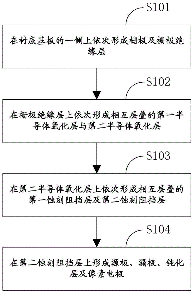
请参阅图1、图4、图5、图6和图7,图1是本实施例的显示基板100的制作方法一实施方式的形成钝化层19与像素电极20层后的部分剖面结构示意图,图4是本实施例的显示基板100的制作方法一实施方式的部分实施步骤流程图,图5是本实施例的显示基板100的制作方法一实施方式的形成第一蚀刻阻挡层15与第二蚀刻阻挡层16后的部分剖面结构示意图,图6是本实施例的显示基板100的制作方法一实施方式的形成第一半导体氧化层13与第二半导体氧化层14后的部分剖面结构示意图,图7是本实施例的显示基板100的制作方法一实施方式的形成栅极绝缘层12后的部分剖面结构示意图。Please refer to FIG. 1 , FIG. 4 , FIG. 5 , FIG. 6 and FIG. 7 . FIG. 1 is a schematic diagram of a partial cross-sectional structure of the
本发明的显示基板100的制作方法,包括以下几个步骤:The manufacturing method of the
步骤S101:在衬底基板10的一侧上依次形成栅极11及栅极绝缘层12,其中栅极11形成于衬底基板10的一表面上,栅极绝缘层12形成于栅极11上,并覆盖栅极11和衬底基板10。本步骤形成的结构如图7所示。Step S101 : forming a
本步骤的具体做法如下:The specific steps of this step are as follows:
第一,在透明玻璃基板或者石英上,即在衬底基板10上采用溅射或热蒸发的方法依次沉积上厚度约为


第二,在完成以上步骤的衬底基板10上通过化学气相沉积(PECVD)方法连续沉积厚度为


步骤S102:在栅极绝缘层12上依次形成相互层叠的第一半导体氧化层13与第二半导体氧化层14,其中在所述第一半导体氧化层13的远离所述衬底基板10的一面上设置第二半导体氧化层14。本步骤形成的结构如图6所示。Step S102 : sequentially forming a first
在本步骤中,所述第一半导体氧化层13的导电率低于所述第二半导体氧化层14的导电率,所述第二半导体氧化层14可在蚀刻源极17和漏极18金属层时,作为保护层保护第一半导体氧化层13以使其不受损伤。In this step, the conductivity of the first
本步骤的具体做法如下:The specific steps of this step are as follows:
通过溅射方法在栅极绝缘层12上,连续沉积厚度为


金属氧化物薄膜的材料可选为非晶IGZO(indium gallium zinc oxide),即铟镓锌氧化物,或采用非晶IGZO、HIZO、IZO、a-InZnO、a-InZnO、ZnO:F、In2O3:Sn、In2O3:Mo、Cd2SnO4、ZnO:Al、TiO2:Nb、Cd-Sn-O或其他金属氧化物。The material of the metal oxide film can be selected from amorphous IGZO (indium gallium zinc oxide), that is, indium gallium zinc oxide, or amorphous IGZO, HIZO, IZO, a-InZnO, a-InZnO, ZnO:F, In 2 O 3 :Sn, In 2 O 3 :Mo, Cd 2 SnO 4 , ZnO:Al, TiO 2 :Nb, Cd-Sn-O or other metal oxides.
步骤S103:在第二半导体氧化层14上依次形成相互层叠的第一蚀刻阻挡层15和第二蚀刻阻挡层16,且所述第一蚀刻阻挡层15位于所述第二蚀刻阻挡层16和所述第二半导体氧化层14之间。本步骤形成的结构如图5所示。Step S103 : sequentially forming a first
在本步骤中,所述第一蚀刻阻挡层15可防止所述半导体有源层的氧元素扩散至其外部,避免所述半导体有源层失氧。In this step, the first
本步骤的具体做法如下:The specific steps of this step are as follows:
首先,通过溅射或热蒸发在第二半导体氧化层14上连续沉积厚度约为


步骤S104:在第二蚀刻阻挡层16上形成源极17、漏极18、钝化层19及像素电极20,其中源极17和漏极18形成于第二蚀刻阻挡层16上,钝化层19形成于源极17和漏极18上并覆盖源极17和漏极18,像素电极20形成于部分钝化层19上,并穿过钝化层19和漏极18接触导通。本步骤形成的结构如图1所示。Step S104 : forming a
本步骤的具体做法如下:The specific steps of this step are as follows:
沉积厚度约为


第一,在完成上述步骤的第二蚀刻阻挡层16上通过PECVD方法连续沉积厚度为


第二,在完成上述步骤的钝化层19过孔及其附近的钝化层19上通过溅射或热蒸发的方法连续沉积厚度约为


以上所述仅为本发明的实施方式,并非因此限制本发明的专利范围,凡是利用本发明说明书及附图内容所作的等效结构或等效流程变换,或直接或间接运用在其他相关的技术领域,均同理包括在本发明的专利保护范围内。The above description is only an embodiment of the present invention, and is not intended to limit the scope of the present invention. Any equivalent structure or equivalent process transformation made by using the contents of the description and drawings of the present invention, or directly or indirectly applied to other related technologies Fields are similarly included in the scope of patent protection of the present invention.
Claims (6)


Priority Applications (1)
| Application Number | Priority Date | Filing Date | Title |
|---|---|---|---|
| CN201711200195.4A CN107968097B (en) | 2017-11-24 | 2017-11-24 | Display device, display substrate and manufacturing method thereof |
Applications Claiming Priority (1)
| Application Number | Priority Date | Filing Date | Title |
|---|---|---|---|
| CN201711200195.4A CN107968097B (en) | 2017-11-24 | 2017-11-24 | Display device, display substrate and manufacturing method thereof |
Publications (2)
| Publication Number | Publication Date |
|---|---|
| CN107968097A CN107968097A (en) | 2018-04-27 |
| CN107968097B true CN107968097B (en) | 2020-11-06 |
Family
ID=61998991
Family Applications (1)
| Application Number | Title | Priority Date | Filing Date |
|---|---|---|---|
| CN201711200195.4A Active CN107968097B (en) | 2017-11-24 | 2017-11-24 | Display device, display substrate and manufacturing method thereof |
Country Status (1)
| Country | Link |
|---|---|
| CN (1) | CN107968097B (en) |
Families Citing this family (7)
| Publication number | Priority date | Publication date | Assignee | Title |
|---|---|---|---|---|
| CN109148476A (en) * | 2018-07-09 | 2019-01-04 | 深圳市华星光电半导体显示技术有限公司 | Tft array substrate and preparation method thereof |
| CN110310985A (en) * | 2019-07-05 | 2019-10-08 | 山东大学 | A kind of indium aluminum zinc oxide thin film transistor based on double active layer and its preparation method |
| CN110718561A (en) * | 2019-10-23 | 2020-01-21 | 成都中电熊猫显示科技有限公司 | Manufacturing method of array substrate and array substrate |
| CN110648965B (en) * | 2019-10-23 | 2024-11-12 | 成都京东方显示科技有限公司 | Method for manufacturing array substrate and array substrate |
| CN110707105A (en) * | 2019-10-23 | 2020-01-17 | 成都中电熊猫显示科技有限公司 | Manufacturing method of array substrate and array substrate |
| CN110729238A (en) * | 2019-10-23 | 2020-01-24 | 成都中电熊猫显示科技有限公司 | Fabrication method of array substrate and array substrate |
| CN111403336A (en) * | 2020-03-31 | 2020-07-10 | 成都中电熊猫显示科技有限公司 | Array substrate, display panel and manufacturing method of array substrate |
Family Cites Families (7)
| Publication number | Priority date | Publication date | Assignee | Title |
|---|---|---|---|---|
| TWI399580B (en) * | 2003-07-14 | 2013-06-21 | 半導體能源研究所股份有限公司 | Semiconductor device and display device |
| EP1998373A3 (en) * | 2005-09-29 | 2012-10-31 | Semiconductor Energy Laboratory Co, Ltd. | Semiconductor device having oxide semiconductor layer and manufacturing method thereof |
| KR101895421B1 (en) * | 2011-02-24 | 2018-09-07 | 삼성디스플레이 주식회사 | Wiring, thin film transistor, thin film transistor panel and methods for manufacturing the same |
| CN102769039A (en) * | 2012-01-13 | 2012-11-07 | 京东方科技集团股份有限公司 | A kind of thin film transistor and its manufacturing method, array substrate and display device |
| KR20140021118A (en) * | 2012-08-07 | 2014-02-20 | 삼성디스플레이 주식회사 | Display device and method of manufacturing the same |
| CN103985713B (en) * | 2013-03-20 | 2017-02-08 | 上海天马微电子有限公司 | TFT array substrate and manufacturing method thereof |
| TWI566405B (en) * | 2013-11-08 | 2017-01-11 | 元太科技工業股份有限公司 | Organic-inorganic hybrid transistor |
-
2017
- 2017-11-24 CN CN201711200195.4A patent/CN107968097B/en active Active
Also Published As
| Publication number | Publication date |
|---|---|
| CN107968097A (en) | 2018-04-27 |
Similar Documents
| Publication | Publication Date | Title |
|---|---|---|
| CN107968097B (en) | Display device, display substrate and manufacturing method thereof | |
| KR101325053B1 (en) | Thin film transistor substrate and manufacturing method thereof | |
| US9484363B2 (en) | Liquid crystal display and method of manufacturing the same | |
| KR101447843B1 (en) | Thin film transistor array substrate, method for manufacturing the same, display panel and display device | |
| KR101522481B1 (en) | Method for fabricating array substrate, array substrate and display device | |
| CN103219389B (en) | A kind of thin-film transistor and preparation method thereof, array base palte and display unit | |
| CN103000628B (en) | Display device, array substrate and manufacture method of array substrate | |
| JP5766467B2 (en) | THIN FILM TRANSISTOR, MANUFACTURING METHOD THEREOF, AND DISPLAY DEVICE | |
| US8349630B1 (en) | Methods for manufacturing thin film transistor array substrate and display panel | |
| CN207265054U (en) | A kind of array base palte, display panel and display device | |
| WO2017166341A1 (en) | Method for manufacturing tft substrate and manufactured tft substrate | |
| KR20130140581A (en) | Display device and manufacturing method thereof | |
| KR20110124530A (en) | Oxide semiconductor, thin film transistor and thin film transistor array panel comprising same | |
| JP5215543B2 (en) | Thin film transistor substrate | |
| WO2015043220A1 (en) | Thin film transistor, preparation method therefor, array substrate, and display apparatus | |
| WO2021077674A1 (en) | Method for manufacturing array substrate, and array substrate | |
| CN111403337A (en) | Array substrate, display panel and manufacturing method of array substrate | |
| WO2021077673A1 (en) | Array substrate manufacturing method, and array substrate | |
| CN105070684A (en) | Array substrate preparation method, array substrate and display device | |
| US8558230B2 (en) | Thin film transistor substrate and method of fabricating the same | |
| JP2007053363A5 (en) | ||
| KR20160128518A (en) | Display device and manufacturing method thereof | |
| CN102569293A (en) | Thin film transistor array and circuit structure thereof | |
| CN211554588U (en) | Array substrate and liquid crystal display panel | |
| CN103489900B (en) | A kind of barrier layer and preparation method thereof, thin film transistor (TFT), array base palte |
Legal Events
| Date | Code | Title | Description |
|---|---|---|---|
| PB01 | Publication | ||
| PB01 | Publication | ||
| SE01 | Entry into force of request for substantive examination | ||
| SE01 | Entry into force of request for substantive examination | ||
| GR01 | Patent grant | ||
| GR01 | Patent grant |