CN103562988A - Systems and methods for extracting threshold and mobility parameters in AMOLED displays - Google Patents
Systems and methods for extracting threshold and mobility parameters in AMOLED displays Download PDFInfo
- Publication number
- CN103562988A CN103562988A CN201280022957.5A CN201280022957A CN103562988A CN 103562988 A CN103562988 A CN 103562988A CN 201280022957 A CN201280022957 A CN 201280022957A CN 103562988 A CN103562988 A CN 103562988A
- Authority
- CN
- China
- Prior art keywords
- voltage
- transistor
- oled
- input
- charge pump
- Prior art date
- Legal status (The legal status is an assumption and is not a legal conclusion. Google has not performed a legal analysis and makes no representation as to the accuracy of the status listed.)
- Granted
Links
Images


Classifications
-
- G—PHYSICS
- G09—EDUCATION; CRYPTOGRAPHY; DISPLAY; ADVERTISING; SEALS
- G09G—ARRANGEMENTS OR CIRCUITS FOR CONTROL OF INDICATING DEVICES USING STATIC MEANS TO PRESENT VARIABLE INFORMATION
- G09G3/00—Control arrangements or circuits, of interest only in connection with visual indicators other than cathode-ray tubes
- G09G3/006—Electronic inspection or testing of displays and display drivers, e.g. of LED or LCD displays
-
- G—PHYSICS
- G01—MEASURING; TESTING
- G01R—MEASURING ELECTRIC VARIABLES; MEASURING MAGNETIC VARIABLES
- G01R19/00—Arrangements for measuring currents or voltages or for indicating presence or sign thereof
- G01R19/0092—Arrangements for measuring currents or voltages or for indicating presence or sign thereof measuring current only
-
- G—PHYSICS
- G09—EDUCATION; CRYPTOGRAPHY; DISPLAY; ADVERTISING; SEALS
- G09G—ARRANGEMENTS OR CIRCUITS FOR CONTROL OF INDICATING DEVICES USING STATIC MEANS TO PRESENT VARIABLE INFORMATION
- G09G3/00—Control arrangements or circuits, of interest only in connection with visual indicators other than cathode-ray tubes
- G09G3/20—Control arrangements or circuits, of interest only in connection with visual indicators other than cathode-ray tubes for presentation of an assembly of a number of characters, e.g. a page, by composing the assembly by combination of individual elements arranged in a matrix no fixed position being assigned to or needed to be assigned to the individual characters or partial characters
- G09G3/22—Control arrangements or circuits, of interest only in connection with visual indicators other than cathode-ray tubes for presentation of an assembly of a number of characters, e.g. a page, by composing the assembly by combination of individual elements arranged in a matrix no fixed position being assigned to or needed to be assigned to the individual characters or partial characters using controlled light sources
- G09G3/30—Control arrangements or circuits, of interest only in connection with visual indicators other than cathode-ray tubes for presentation of an assembly of a number of characters, e.g. a page, by composing the assembly by combination of individual elements arranged in a matrix no fixed position being assigned to or needed to be assigned to the individual characters or partial characters using controlled light sources using electroluminescent panels
- G09G3/32—Control arrangements or circuits, of interest only in connection with visual indicators other than cathode-ray tubes for presentation of an assembly of a number of characters, e.g. a page, by composing the assembly by combination of individual elements arranged in a matrix no fixed position being assigned to or needed to be assigned to the individual characters or partial characters using controlled light sources using electroluminescent panels semiconductive, e.g. using light-emitting diodes [LED]
- G09G3/3208—Control arrangements or circuits, of interest only in connection with visual indicators other than cathode-ray tubes for presentation of an assembly of a number of characters, e.g. a page, by composing the assembly by combination of individual elements arranged in a matrix no fixed position being assigned to or needed to be assigned to the individual characters or partial characters using controlled light sources using electroluminescent panels semiconductive, e.g. using light-emitting diodes [LED] organic, e.g. using organic light-emitting diodes [OLED]
- G09G3/3225—Control arrangements or circuits, of interest only in connection with visual indicators other than cathode-ray tubes for presentation of an assembly of a number of characters, e.g. a page, by composing the assembly by combination of individual elements arranged in a matrix no fixed position being assigned to or needed to be assigned to the individual characters or partial characters using controlled light sources using electroluminescent panels semiconductive, e.g. using light-emitting diodes [LED] organic, e.g. using organic light-emitting diodes [OLED] using an active matrix
- G09G3/3233—Control arrangements or circuits, of interest only in connection with visual indicators other than cathode-ray tubes for presentation of an assembly of a number of characters, e.g. a page, by composing the assembly by combination of individual elements arranged in a matrix no fixed position being assigned to or needed to be assigned to the individual characters or partial characters using controlled light sources using electroluminescent panels semiconductive, e.g. using light-emitting diodes [LED] organic, e.g. using organic light-emitting diodes [OLED] using an active matrix with pixel circuitry controlling the current through the light-emitting element
-
- G—PHYSICS
- G09—EDUCATION; CRYPTOGRAPHY; DISPLAY; ADVERTISING; SEALS
- G09G—ARRANGEMENTS OR CIRCUITS FOR CONTROL OF INDICATING DEVICES USING STATIC MEANS TO PRESENT VARIABLE INFORMATION
- G09G3/00—Control arrangements or circuits, of interest only in connection with visual indicators other than cathode-ray tubes
- G09G3/20—Control arrangements or circuits, of interest only in connection with visual indicators other than cathode-ray tubes for presentation of an assembly of a number of characters, e.g. a page, by composing the assembly by combination of individual elements arranged in a matrix no fixed position being assigned to or needed to be assigned to the individual characters or partial characters
- G09G3/22—Control arrangements or circuits, of interest only in connection with visual indicators other than cathode-ray tubes for presentation of an assembly of a number of characters, e.g. a page, by composing the assembly by combination of individual elements arranged in a matrix no fixed position being assigned to or needed to be assigned to the individual characters or partial characters using controlled light sources
- G09G3/30—Control arrangements or circuits, of interest only in connection with visual indicators other than cathode-ray tubes for presentation of an assembly of a number of characters, e.g. a page, by composing the assembly by combination of individual elements arranged in a matrix no fixed position being assigned to or needed to be assigned to the individual characters or partial characters using controlled light sources using electroluminescent panels
- G09G3/32—Control arrangements or circuits, of interest only in connection with visual indicators other than cathode-ray tubes for presentation of an assembly of a number of characters, e.g. a page, by composing the assembly by combination of individual elements arranged in a matrix no fixed position being assigned to or needed to be assigned to the individual characters or partial characters using controlled light sources using electroluminescent panels semiconductive, e.g. using light-emitting diodes [LED]
- G09G3/3208—Control arrangements or circuits, of interest only in connection with visual indicators other than cathode-ray tubes for presentation of an assembly of a number of characters, e.g. a page, by composing the assembly by combination of individual elements arranged in a matrix no fixed position being assigned to or needed to be assigned to the individual characters or partial characters using controlled light sources using electroluminescent panels semiconductive, e.g. using light-emitting diodes [LED] organic, e.g. using organic light-emitting diodes [OLED]
- G09G3/3225—Control arrangements or circuits, of interest only in connection with visual indicators other than cathode-ray tubes for presentation of an assembly of a number of characters, e.g. a page, by composing the assembly by combination of individual elements arranged in a matrix no fixed position being assigned to or needed to be assigned to the individual characters or partial characters using controlled light sources using electroluminescent panels semiconductive, e.g. using light-emitting diodes [LED] organic, e.g. using organic light-emitting diodes [OLED] using an active matrix
- G09G3/3258—Control arrangements or circuits, of interest only in connection with visual indicators other than cathode-ray tubes for presentation of an assembly of a number of characters, e.g. a page, by composing the assembly by combination of individual elements arranged in a matrix no fixed position being assigned to or needed to be assigned to the individual characters or partial characters using controlled light sources using electroluminescent panels semiconductive, e.g. using light-emitting diodes [LED] organic, e.g. using organic light-emitting diodes [OLED] using an active matrix with pixel circuitry controlling the voltage across the light-emitting element
-
- G—PHYSICS
- G09—EDUCATION; CRYPTOGRAPHY; DISPLAY; ADVERTISING; SEALS
- G09G—ARRANGEMENTS OR CIRCUITS FOR CONTROL OF INDICATING DEVICES USING STATIC MEANS TO PRESENT VARIABLE INFORMATION
- G09G3/00—Control arrangements or circuits, of interest only in connection with visual indicators other than cathode-ray tubes
- G09G3/20—Control arrangements or circuits, of interest only in connection with visual indicators other than cathode-ray tubes for presentation of an assembly of a number of characters, e.g. a page, by composing the assembly by combination of individual elements arranged in a matrix no fixed position being assigned to or needed to be assigned to the individual characters or partial characters
- G09G3/22—Control arrangements or circuits, of interest only in connection with visual indicators other than cathode-ray tubes for presentation of an assembly of a number of characters, e.g. a page, by composing the assembly by combination of individual elements arranged in a matrix no fixed position being assigned to or needed to be assigned to the individual characters or partial characters using controlled light sources
- G09G3/30—Control arrangements or circuits, of interest only in connection with visual indicators other than cathode-ray tubes for presentation of an assembly of a number of characters, e.g. a page, by composing the assembly by combination of individual elements arranged in a matrix no fixed position being assigned to or needed to be assigned to the individual characters or partial characters using controlled light sources using electroluminescent panels
- G09G3/32—Control arrangements or circuits, of interest only in connection with visual indicators other than cathode-ray tubes for presentation of an assembly of a number of characters, e.g. a page, by composing the assembly by combination of individual elements arranged in a matrix no fixed position being assigned to or needed to be assigned to the individual characters or partial characters using controlled light sources using electroluminescent panels semiconductive, e.g. using light-emitting diodes [LED]
- G09G3/3208—Control arrangements or circuits, of interest only in connection with visual indicators other than cathode-ray tubes for presentation of an assembly of a number of characters, e.g. a page, by composing the assembly by combination of individual elements arranged in a matrix no fixed position being assigned to or needed to be assigned to the individual characters or partial characters using controlled light sources using electroluminescent panels semiconductive, e.g. using light-emitting diodes [LED] organic, e.g. using organic light-emitting diodes [OLED]
- G09G3/3266—Details of drivers for scan electrodes
-
- G—PHYSICS
- G09—EDUCATION; CRYPTOGRAPHY; DISPLAY; ADVERTISING; SEALS
- G09G—ARRANGEMENTS OR CIRCUITS FOR CONTROL OF INDICATING DEVICES USING STATIC MEANS TO PRESENT VARIABLE INFORMATION
- G09G3/00—Control arrangements or circuits, of interest only in connection with visual indicators other than cathode-ray tubes
- G09G3/20—Control arrangements or circuits, of interest only in connection with visual indicators other than cathode-ray tubes for presentation of an assembly of a number of characters, e.g. a page, by composing the assembly by combination of individual elements arranged in a matrix no fixed position being assigned to or needed to be assigned to the individual characters or partial characters
- G09G3/22—Control arrangements or circuits, of interest only in connection with visual indicators other than cathode-ray tubes for presentation of an assembly of a number of characters, e.g. a page, by composing the assembly by combination of individual elements arranged in a matrix no fixed position being assigned to or needed to be assigned to the individual characters or partial characters using controlled light sources
- G09G3/30—Control arrangements or circuits, of interest only in connection with visual indicators other than cathode-ray tubes for presentation of an assembly of a number of characters, e.g. a page, by composing the assembly by combination of individual elements arranged in a matrix no fixed position being assigned to or needed to be assigned to the individual characters or partial characters using controlled light sources using electroluminescent panels
- G09G3/32—Control arrangements or circuits, of interest only in connection with visual indicators other than cathode-ray tubes for presentation of an assembly of a number of characters, e.g. a page, by composing the assembly by combination of individual elements arranged in a matrix no fixed position being assigned to or needed to be assigned to the individual characters or partial characters using controlled light sources using electroluminescent panels semiconductive, e.g. using light-emitting diodes [LED]
- G09G3/3208—Control arrangements or circuits, of interest only in connection with visual indicators other than cathode-ray tubes for presentation of an assembly of a number of characters, e.g. a page, by composing the assembly by combination of individual elements arranged in a matrix no fixed position being assigned to or needed to be assigned to the individual characters or partial characters using controlled light sources using electroluminescent panels semiconductive, e.g. using light-emitting diodes [LED] organic, e.g. using organic light-emitting diodes [OLED]
- G09G3/3275—Details of drivers for data electrodes
- G09G3/3291—Details of drivers for data electrodes in which the data driver supplies a variable data voltage for setting the current through, or the voltage across, the light-emitting elements
-
- H—ELECTRICITY
- H03—ELECTRONIC CIRCUITRY
- H03F—AMPLIFIERS
- H03F3/00—Amplifiers with only discharge tubes or only semiconductor devices as amplifying elements
- H03F3/20—Power amplifiers, e.g. Class B amplifiers, Class C amplifiers
- H03F3/21—Power amplifiers, e.g. Class B amplifiers, Class C amplifiers with semiconductor devices only
- H03F3/217—Class D power amplifiers; Switching amplifiers
- H03F3/2171—Class D power amplifiers; Switching amplifiers with field-effect devices
-
- G—PHYSICS
- G09—EDUCATION; CRYPTOGRAPHY; DISPLAY; ADVERTISING; SEALS
- G09G—ARRANGEMENTS OR CIRCUITS FOR CONTROL OF INDICATING DEVICES USING STATIC MEANS TO PRESENT VARIABLE INFORMATION
- G09G2300/00—Aspects of the constitution of display devices
- G09G2300/04—Structural and physical details of display devices
- G09G2300/0421—Structural details of the set of electrodes
- G09G2300/043—Compensation electrodes or other additional electrodes in matrix displays related to distortions or compensation signals, e.g. for modifying TFT threshold voltage in column driver
-
- G—PHYSICS
- G09—EDUCATION; CRYPTOGRAPHY; DISPLAY; ADVERTISING; SEALS
- G09G—ARRANGEMENTS OR CIRCUITS FOR CONTROL OF INDICATING DEVICES USING STATIC MEANS TO PRESENT VARIABLE INFORMATION
- G09G2300/00—Aspects of the constitution of display devices
- G09G2300/04—Structural and physical details of display devices
- G09G2300/0439—Pixel structures
- G09G2300/0465—Improved aperture ratio, e.g. by size reduction of the pixel circuit, e.g. for improving the pixel density or the maximum displayable luminance or brightness
-
- G—PHYSICS
- G09—EDUCATION; CRYPTOGRAPHY; DISPLAY; ADVERTISING; SEALS
- G09G—ARRANGEMENTS OR CIRCUITS FOR CONTROL OF INDICATING DEVICES USING STATIC MEANS TO PRESENT VARIABLE INFORMATION
- G09G2300/00—Aspects of the constitution of display devices
- G09G2300/08—Active matrix structure, i.e. with use of active elements, inclusive of non-linear two terminal elements, in the pixels together with light emitting or modulating elements
- G09G2300/0809—Several active elements per pixel in active matrix panels
- G09G2300/0819—Several active elements per pixel in active matrix panels used for counteracting undesired variations, e.g. feedback or autozeroing
-
- G—PHYSICS
- G09—EDUCATION; CRYPTOGRAPHY; DISPLAY; ADVERTISING; SEALS
- G09G—ARRANGEMENTS OR CIRCUITS FOR CONTROL OF INDICATING DEVICES USING STATIC MEANS TO PRESENT VARIABLE INFORMATION
- G09G2300/00—Aspects of the constitution of display devices
- G09G2300/08—Active matrix structure, i.e. with use of active elements, inclusive of non-linear two terminal elements, in the pixels together with light emitting or modulating elements
- G09G2300/0809—Several active elements per pixel in active matrix panels
- G09G2300/0842—Several active elements per pixel in active matrix panels forming a memory circuit, e.g. a dynamic memory with one capacitor
- G09G2300/0861—Several active elements per pixel in active matrix panels forming a memory circuit, e.g. a dynamic memory with one capacitor with additional control of the display period without amending the charge stored in a pixel memory, e.g. by means of additional select electrodes
- G09G2300/0866—Several active elements per pixel in active matrix panels forming a memory circuit, e.g. a dynamic memory with one capacitor with additional control of the display period without amending the charge stored in a pixel memory, e.g. by means of additional select electrodes by means of changes in the pixel supply voltage
-
- G—PHYSICS
- G09—EDUCATION; CRYPTOGRAPHY; DISPLAY; ADVERTISING; SEALS
- G09G—ARRANGEMENTS OR CIRCUITS FOR CONTROL OF INDICATING DEVICES USING STATIC MEANS TO PRESENT VARIABLE INFORMATION
- G09G2310/00—Command of the display device
- G09G2310/02—Addressing, scanning or driving the display screen or processing steps related thereto
- G09G2310/0243—Details of the generation of driving signals
- G09G2310/0251—Precharge or discharge of pixel before applying new pixel voltage
-
- G—PHYSICS
- G09—EDUCATION; CRYPTOGRAPHY; DISPLAY; ADVERTISING; SEALS
- G09G—ARRANGEMENTS OR CIRCUITS FOR CONTROL OF INDICATING DEVICES USING STATIC MEANS TO PRESENT VARIABLE INFORMATION
- G09G2310/00—Command of the display device
- G09G2310/02—Addressing, scanning or driving the display screen or processing steps related thereto
- G09G2310/0264—Details of driving circuits
- G09G2310/0291—Details of output amplifiers or buffers arranged for use in a driving circuit
-
- G—PHYSICS
- G09—EDUCATION; CRYPTOGRAPHY; DISPLAY; ADVERTISING; SEALS
- G09G—ARRANGEMENTS OR CIRCUITS FOR CONTROL OF INDICATING DEVICES USING STATIC MEANS TO PRESENT VARIABLE INFORMATION
- G09G2310/00—Command of the display device
- G09G2310/08—Details of timing specific for flat panels, other than clock recovery
-
- G—PHYSICS
- G09—EDUCATION; CRYPTOGRAPHY; DISPLAY; ADVERTISING; SEALS
- G09G—ARRANGEMENTS OR CIRCUITS FOR CONTROL OF INDICATING DEVICES USING STATIC MEANS TO PRESENT VARIABLE INFORMATION
- G09G2320/00—Control of display operating conditions
- G09G2320/02—Improving the quality of display appearance
- G09G2320/0233—Improving the luminance or brightness uniformity across the screen
-
- G—PHYSICS
- G09—EDUCATION; CRYPTOGRAPHY; DISPLAY; ADVERTISING; SEALS
- G09G—ARRANGEMENTS OR CIRCUITS FOR CONTROL OF INDICATING DEVICES USING STATIC MEANS TO PRESENT VARIABLE INFORMATION
- G09G2320/00—Control of display operating conditions
- G09G2320/02—Improving the quality of display appearance
- G09G2320/029—Improving the quality of display appearance by monitoring one or more pixels in the display panel, e.g. by monitoring a fixed reference pixel
- G09G2320/0295—Improving the quality of display appearance by monitoring one or more pixels in the display panel, e.g. by monitoring a fixed reference pixel by monitoring each display pixel
-
- G—PHYSICS
- G09—EDUCATION; CRYPTOGRAPHY; DISPLAY; ADVERTISING; SEALS
- G09G—ARRANGEMENTS OR CIRCUITS FOR CONTROL OF INDICATING DEVICES USING STATIC MEANS TO PRESENT VARIABLE INFORMATION
- G09G2320/00—Control of display operating conditions
- G09G2320/04—Maintaining the quality of display appearance
- G09G2320/043—Preventing or counteracting the effects of ageing
- G09G2320/045—Compensation of drifts in the characteristics of light emitting or modulating elements
-
- G—PHYSICS
- G09—EDUCATION; CRYPTOGRAPHY; DISPLAY; ADVERTISING; SEALS
- G09G—ARRANGEMENTS OR CIRCUITS FOR CONTROL OF INDICATING DEVICES USING STATIC MEANS TO PRESENT VARIABLE INFORMATION
- G09G2330/00—Aspects of power supply; Aspects of display protection and defect management
- G09G2330/02—Details of power systems and of start or stop of display operation
- G09G2330/028—Generation of voltages supplied to electrode drivers in a matrix display other than LCD
Landscapes
- Engineering & Computer Science (AREA)
- Physics & Mathematics (AREA)
- General Physics & Mathematics (AREA)
- Computer Hardware Design (AREA)
- Theoretical Computer Science (AREA)
- Power Engineering (AREA)
- Control Of Indicators Other Than Cathode Ray Tubes (AREA)
- Control Of El Displays (AREA)
- Electroluminescent Light Sources (AREA)
Abstract
Description
版权copyright
本专利文件的部分公开内容包含受版权保护的材料。版权所有人不反对任何人按照本专利公开在美国专利和商标局的专利文档或记录中所呈现的形式对本专利公开进行复制,但是无论如何都保留所有版权。Portions of the disclosure of this patent document contain material that is protected by copyright. The copyright owner has no objection to the reproduction by anyone of the patent disclosure as it appears in the patent file or records of the United States Patent and Trademark Office, but all copyrights are reserved regardless.
技术领域technical field
本发明一般地涉及一种有源矩阵有机发光器件(AMOLED)显示器,具体地涉及从用于这种显示器的像素驱动器提取阈值和迁移因数。The present invention relates generally to an active matrix organic light emitting device (AMOLED) display, and in particular to extracting threshold and transfer factors from a pixel driver for such a display.
背景技术Background technique
目前,正引入一种有源矩阵有机发光器件(“AMOLED”)显示器。这种显示器和传统液晶显示器相比的优点包括低功耗、制造灵活以及刷新速率更快。与传统液晶显示器相比,AMOLED显示器无背光,因此各个像素由独立发光的不同颜色的OLED组成。OLED基于通过驱动晶体管提供的电流而发光,该驱动晶体管由编程电压控制。各个像素的功耗与该像素中产生的光的大小有关。Currently, an active matrix organic light emitting device ("AMOLED") display is being introduced. Advantages of such displays over conventional LCDs include low power consumption, manufacturing flexibility, and faster refresh rates. Compared with traditional LCD displays, AMOLED displays have no backlight, so each pixel is composed of OLEDs of different colors that emit light independently. OLEDs emit light based on current supplied through a drive transistor controlled by a programming voltage. The power consumption of each pixel is related to the amount of light generated in that pixel.
基于OLED的像素中的输出质量受到驱动晶体管以及OLED本身的性能的影响,驱动晶体管通常由包括但不限于非晶硅、多晶硅或金属氧化物等的材料制成。尤其,随着像素的老化,驱动晶体管的阈值电压和迁移率均会改变。为了保持图像质量,这些参数发生的变化必须通过调整编程电压来进行补偿。为了实施该过程,这些参数必须从驱动电路中提取出来。为提取简单驱动电路中的这些参数而增加的元件要求在显示器基板上为该驱动电路要有更多的空间,因此也就减少了从OLED进行发光的孔径或面积的大小。The output quality in an OLED-based pixel is affected by the performance of the drive transistor, which is typically made of materials including but not limited to amorphous silicon, polysilicon, or metal oxides, as well as the OLED itself. In particular, as the pixel ages, both the threshold voltage and the mobility of the drive transistor change. To maintain image quality, changes in these parameters must be compensated by adjusting the programming voltage. In order to implement the process, these parameters must be extracted from the drive circuit. The added components to extract these parameters in a simple driver circuit requires more space on the display substrate for the driver circuit, thus reducing the size of the aperture or area for emitting light from the OLED.
当偏置在饱和时,薄膜驱动晶体管的I-V特性取决于迁移率和阈值电压,该迁移率和阈值电压是用于制造晶体管的材料的函数。因此,受老化和迁移率和阈值电压的工艺偏差的影响,在整个显示器面板上设置的不同薄膜晶体管器件可能会呈现出不一致的行为。于是,对于恒定的电压,各个器件可具有不同的漏极电流。在极端的示例中,一个器件可具有低阈值电压和低迁移率,而相比之下,第二个器件可具有高阈值电压和高迁移率。When biased at saturation, the I-V characteristics of a thin film drive transistor depend on the mobility and threshold voltage, which are a function of the material used to fabricate the transistor. Therefore, different TFT devices disposed across a display panel may exhibit inconsistent behavior due to aging and process variations in mobility and threshold voltage. Thus, for a constant voltage, individual devices may have different drain currents. In an extreme example, one device may have a low threshold voltage and low mobility, while in contrast a second device may have a high threshold voltage and high mobility.
因此,当仅有很少的电子元件可用于保持所需的孔径时,提取驱动TFT和OLED的非一致性参数(即,阈值电压Vth和迁移率μ)变得具有挑战性。本发明期望以尽可能少的元件提取OLED像素的驱动电路中的这类参数以使像素孔径最大化。Therefore, it becomes challenging to extract non-uniform parameters driving TFTs and OLEDs (i.e., threshold voltage V and mobility μ) when only few electronic components are available to maintain the desired aperture. The present invention contemplates extracting such parameters in the driver circuit of an OLED pixel with as few components as possible to maximize the pixel aperture.
发明内容Contents of the invention
本发明的一个示例中公开了一种用于基于有机发光器件(OLED)的显示器的数据提取系统。所述系统包括:像素电路,其包括有机发光器件、用于向所述发光器件提供可编程驱动电流的驱动装置、用于提供编程信号的编程输入和用于储存所述编程信号的储存装置。电荷泵放大器具有电流输入和电压输出。所述电荷泵放大器包括呈负反馈结构的运算放大器。所述反馈由连接在所述运算放大器的输出与反相输入之间的电容器提供。共模电压源驱动所述运算放大器的非反相输入。在所述电容器上跨接有电子开关以重置所述电容器。开关模块包括与所述像素电路的输出连接的输入以及与所述电荷泵放大器的输入连接的输出。所述开关模块包括多个电子开关,以用于将电流导入和导出所述像素电路、在所述像素电路与所述电荷泵放大器之间提供放电路径、并使所述电荷泵放大器与所述像素电路隔开。控制器与所述像素电路、所述电荷泵放大器和所述开关模块连接。所述控制器以预定顺序控制施加至所述像素电路、所述电荷泵放大器和所述开关模块的输入信号以产生输出电压值,所述输出电压值是所述像素电路的参数的函数。所述顺序包括向所述编程输入提供编程电压,从而:将所述像素电路的内部电容预充电至一定电荷量,并经由所述开关模块将所述电荷传输至所述电荷泵放大器以生成所述输出电压值;或者通过将来自所述像素电路的电流经由所述开关模块提供至所述电荷泵放大器,以通过在特定时间段内进行积分而生成所述输出电压值。In one example of the present invention, a data extraction system for an organic light emitting device (OLED) based display is disclosed. The system includes a pixel circuit including an organic light emitting device, drive means for providing a programmable drive current to the light emitting device, a programming input for providing a programming signal, and storage means for storing the programming signal. A charge pump amplifier has a current input and a voltage output. The charge pump amplifier includes an operational amplifier in a negative feedback structure. The feedback is provided by a capacitor connected between the output and inverting input of the operational amplifier. A common-mode voltage source drives the non-inverting input of the operational amplifier. An electronic switch is connected across the capacitor to reset the capacitor. A switch module includes an input connected to the output of the pixel circuit and an output connected to the input of the charge pump amplifier. The switch module includes a plurality of electronic switches for directing current into and out of the pixel circuit, providing a discharge path between the pixel circuit and the charge pump amplifier, and connecting the charge pump amplifier with the The pixel circuits are separated. The controller is connected with the pixel circuit, the charge pump amplifier and the switch module. The controller controls input signals applied to the pixel circuit, the charge pump amplifier, and the switch module in a predetermined sequence to generate an output voltage value that is a function of parameters of the pixel circuit. The sequence includes providing a programming voltage to the programming input to: precharge an internal capacitance of the pixel circuit to an amount of charge and transfer the charge to the charge pump amplifier via the switch module to generate the the output voltage value; or by supplying the current from the pixel circuit to the charge pump amplifier via the switch module to generate the output voltage value by integrating for a certain period of time.
另一个示例是一种用于从包括有机发光器件的像素电路提取电路参数的方法,所述像素电路包括有机发光器件、用于向所述发光器件提供可编程驱动电流的驱动装置、编程输入和用于储存编程信号的储存装置。向所述编程电压输入提供预定编程电压。将所述像素电路的电容充电至一定电荷量或所述像素电路的电流。使所述像素电路与电荷泵放大器连接。使所述电荷泵放大器与所述像素电路隔开,从而提供一个与所述电荷量成比例的电压输出或者对来自所述像素电路的电流进行积分。读取所述电荷泵放大器的电压输出。从所述电荷泵放大器的电压输出确定至少一个像素电路参数。Another example is a method for extracting circuit parameters from a pixel circuit comprising an organic light emitting device, drive means for providing a programmable drive current to the light emitting device, a programming input and A storage device for storing programming signals. A predetermined programming voltage is provided to the programming voltage input. Charge the capacitance of the pixel circuit to a certain amount of charge or the current of the pixel circuit. The pixel circuit is connected to a charge pump amplifier. The charge pump amplifier is isolated from the pixel circuit to provide a voltage output proportional to the amount of charge or to integrate the current from the pixel circuit. Read the voltage output of the charge pump amplifier. At least one pixel circuit parameter is determined from the voltage output of the charge pump amplifier.
另一个示例是一种用于基于有机发光器件(OLED)的显示器的数据提取系统。所述系统包括像素电路,所述像素电路具有驱动晶体管、有机发光器件和与所述驱动晶体管的栅极连接的编程输入。所述驱动晶体管具有连接至所述OLED的源极或漏极。电荷泵放大器具有输入和积分电压输出。开关模块包括与所述像素电路的输出连接的输入和与所述电荷泵放大器的输入连接的输出。所述开关模块包括用于将电流导入和导出所述像素电路、在所述像素电路与所述电荷泵放大器之间提供放电路径、并将所述电荷泵放大器与所述像素电路隔开的开关。控制器与所述像素电路、所述电荷泵放大器和所述开关模块连接。所述控制器以预定顺序控制施加至所述像素电路、所述电荷泵放大器和所述开关模块的电压输入以生成输出电压值,所述输出电压值是所述像素电路的参数的函数。所述顺序包括向所述编程输入提供编程电压,从而:将所述像素电路的电容预充电至一定电荷量,并经由所述开关模块将所述电荷传输至所述电荷泵放大器以生成所述输出电压值,或者,通过将来自所述像素电路的电流经由所述开关模块提供至所述电荷泵放大器,以通过积分而生成所述输出电压值。Another example is a data extraction system for an organic light emitting device (OLED) based display. The system includes a pixel circuit having a drive transistor, an organic light emitting device, and a programming input connected to a gate of the drive transistor. The driving transistor has a source or a drain connected to the OLED. A charge pump amplifier has an input and an integrating voltage output. A switch module includes an input connected to the output of the pixel circuit and an output connected to the input of the charge pump amplifier. The switch module includes a switch for directing current into and out of the pixel circuit, providing a discharge path between the pixel circuit and the charge pump amplifier, and isolating the charge pump amplifier from the pixel circuit . The controller is connected with the pixel circuit, the charge pump amplifier and the switch module. The controller controls voltage inputs applied to the pixel circuit, the charge pump amplifier, and the switch module in a predetermined sequence to generate an output voltage value that is a function of a parameter of the pixel circuit. The sequence includes providing a programming voltage to the programming input to: precharge the capacitance of the pixel circuit to an amount of charge and transfer the charge to the charge pump amplifier via the switch module to generate the output voltage value, or by providing current from the pixel circuit to the charge pump amplifier via the switch module to generate the output voltage value by integration.
对本领域的普通技术人员而言,参照附图对各种实施例和/或方面进行的详细说明,本发明的上述及其它方面和实施例将是显而易见的。下面将对附图进行简要说明。The above and other aspects and embodiments of the present invention will become apparent to those of ordinary skill in the art from the detailed description of various embodiments and/or aspects with reference to the accompanying drawings. The accompanying drawings will be briefly described below.
附图说明Description of drawings
通过阅读下面的详细说明并参照附图,本发明的上述和其它优点将会变得显而易见。These and other advantages of the present invention will become apparent upon reading the following detailed description and referring to the accompanying drawings.
图1是具有补偿控制的AMOLED显示器的方块图。Figure 1 is a block diagram of an AMOLED display with compensation control.
图2是用于图1所示AMOLED显示器中的二晶体管像素的数据提取电路的电路图;2 is a circuit diagram of a data extraction circuit for a two-transistor pixel in the AMOLED display shown in FIG. 1;
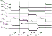
图3A是施加至数据提取电路以提取图2所示n型驱动晶体管的阈值电压和迁移率的信号的信号时序图;3A is a signal timing diagram of signals applied to the data extraction circuit to extract the threshold voltage and mobility of the n-type drive transistor shown in FIG. 2;
图3B是施加至数据提取电路以提取图2所示的具有n型驱动晶体管的OLED的特征电压的信号的信号时序图;3B is a signal timing diagram of signals applied to the data extraction circuit to extract the characteristic voltage of the OLED with n-type drive transistor shown in FIG. 2;
图3C是施加至可直接读取的数据提取电路以提取图2所示n型驱动晶体管的阈值电压的信号的信号时序图;3C is a signal timing diagram of a signal applied to a directly readable data extraction circuit to extract the threshold voltage of the n-type drive transistor shown in FIG. 2;
图4A是施加至数据提取电路以提取图2所示p型驱动晶体管的阈值电压和迁移率的信号的信号时序图;4A is a signal timing diagram of signals applied to the data extraction circuit to extract the threshold voltage and mobility of the p-type drive transistor shown in FIG. 2;
图4B是施加至数据提取电路以提取图2所示的具有p型驱动晶体管的OLED的特征电压的信号的信号时序图;4B is a signal timing diagram of signals applied to the data extraction circuit to extract the characteristic voltage of the OLED with the p-type drive transistor shown in FIG. 2;
图4C是施加至可直接读取的数据提取电路以提取图2所示p型驱动晶体管的阈值电压的信号的信号时序图;4C is a signal timing diagram of a signal applied to a directly readable data extraction circuit to extract the threshold voltage of the p-type drive transistor shown in FIG. 2;
图4D是施加至数据提取电路以通过使用图2所示n型或p型驱动晶体管而直接读取OLED的导通电压的信号的信号时序图;4D is a signal timing diagram of signals applied to the data extraction circuit to directly read the conduction voltage of the OLED by using the n-type or p-type drive transistor shown in FIG. 2;
图5是用于图1所示AMOLED显示器中的一个像素的三晶体管驱动电路的数据提取电路从而提取参数的电路图;Fig. 5 is a circuit diagram for extracting parameters from a data extraction circuit of a three-transistor drive circuit of a pixel in the AMOLED display shown in Fig. 1;
图6A是施加至数据提取电路以提取图5所示驱动晶体管的阈值电压和迁移率的信号的信号时序图;6A is a signal timing diagram of signals applied to the data extraction circuit to extract the threshold voltage and mobility of the driving transistor shown in FIG. 5;
图6B是施加至数据提取电路以提取图5所示OLED的特征电压的信号的信号时序图;6B is a signal timing diagram of signals applied to the data extraction circuit to extract the characteristic voltage of the OLED shown in FIG. 5;
图6C是施加至可直接读取的数据提取电路以提取图5所示驱动晶体管的阈值电压的信号的信号时序图;6C is a signal timing diagram of a signal applied to a directly readable data extraction circuit to extract the threshold voltage of the driving transistor shown in FIG. 5;
图6D是施加至可直接读取的数据提取电路以提取图5所示OLED的特征电压的信号的信号时序图;6D is a signal timing diagram of a signal applied to a directly readable data extraction circuit to extract the characteristic voltage of the OLED shown in FIG. 5;
图7是读取AMOLED显示器中像素电路的驱动晶体管和OLED的特征的提取周期的流程图;7 is a flow chart of an extraction cycle for reading features of a drive transistor and an OLED of a pixel circuit in an AMOLED display;
图8是不同参数提取周期和最终应用的流程图;Figure 8 is a flowchart of different parameter extraction cycles and final applications;
图9是数据提取系统的部件的方块图和图表。Figure 9 is a block diagram and diagram of components of the data extraction system.
尽管本发明可有多种变换和替代形式,但是已通过示例的形式在图中示出了一些具体实施例,并将在本文对这些具体实施例进行详细说明。然而,应理解,本发明并不限于所公开的特定形式。相反,本发明旨在涵盖所有落入所附权利要求限定的本发明精神和范围内的所有变换、等同物和替代物。While the invention is capable of many modifications and alternative forms, specific embodiments have been shown in the drawings by way of example and will be described in detail herein. However, it should be understood that the invention is not intended to be limited to the particular forms disclosed. On the contrary, the invention is intended to cover all modifications, equivalents and alternatives falling within the spirit and scope of the invention as defined by the appended claims.
具体实施方式Detailed ways
图1是电子显示系统100,该系统100具有像素阵列102的有源矩阵区域,其中,像素104的n×m阵列按行和列的形式布置。为了便于说明,仅示出了两行与两列。像素阵列102的有源矩阵区域之外为外围区域106,用于驱动和控制像素阵列102的外围电路设置在外围区域106中。外围电路包括地址或栅极驱动电路108、数据或源极驱动电路110、控制器112以及可选的供给电压(例如Vdd)驱动器114。控制器112控制栅极、源极和供给电压驱动器108、110和114。栅极驱动器108在控制器112的控制下对地址或选择线SEL[i]、SEL[i+1]等进行操作,该地址或选择线与像素阵列102中各行像素104一一对应。在下面说明的像素共享配置中,栅极或地址驱动电路108也可选择性地对全局选择线GSEL[j]和/[GSEL[j]进行操作,所述全局选择线对像素阵列102的多行像素104(比如每两行像素104)进行操作。源极驱动电路110在控制器112的控制下对电压数据线Vdata[k]和Vdata[k+1]等进行操作,该电压数据线与像素阵列102中各列像素104一一对应。电压数据线将指示像素104中各个发光器件的亮度的电压编程信息传送至各个像素104。各个像素104中的储存元件(比如电容器)储存该电压编程信息,一直到发光或驱动周期导通发光器件为止。可选的供给电压驱动器114在控制器112的控制下控制供给电压(EL_Vdd)线,该供给电压线与像素阵列102中各行或各列像素104一一对应。Figure 1 is an
显示系统100还包括电流供给和读出电路120,其读出来自数据输出线VD[k]和VD[k+1]等上的输出数据,该数据输出线线与像素阵列102中的各列像素104一一对应。The
众所周知,显示系统100中的各个像素104都需要用指示像素104中发光器件的亮度的信息进行编程。帧对时间段进行限定,该时间段包括:(i)编程周期或阶段,在此期间,显示系统100中的每一个像素用指示亮度的编程电压进行编程,以及(ii)驱动或发光周期或阶段,在此期间,各个像素中的各个发光器件导通以发光,光的亮度与储存在储存元件中的编程电压相称。因此,帧是许多静止图像之一,这些静止图像组成一个在显示系统100上显示的完整运动画面。用于编程或驱动像素的方案至少有:逐行或逐帧。在逐行编程中,首先对一行像素进行编程再驱动,然后再对下一行像素进行编程和驱动。在逐帧编程中,首先对显示系统100中所有行的像素进行编程,然后再立即驱动所有行的像素。两种方案都可在各个帧开始或结束时采用短暂的垂直消隐时间,在此期间,像素既没被编程也没被驱动。As is well known, each
位于像素阵列102外面的部件可设置在像素阵列102周围的外围区域106中并与像素阵列102设置在同一物理基板上。这些部件包括栅极驱动器108、源极驱动器110、可选的供给电压驱动器114以及电流供给和读出电路120。或者,外围区域106中的一些部件可与像素阵列102设置在同一基板上,而另一些部件则设置在不同的基板上,或者外围区域中的所有部件都可设置在与设置像素阵列102的基板不同的基板上。栅极驱动器108、源极驱动器110和供给电压驱动器114一起构成显示驱动电路。在一些配置中,显示驱动电路可包括栅极驱动器108和源极驱动器110,但不包括供给电压控制114。Components located outside of
当偏置在饱和时,金属氧化物半导体(MOS)晶体管(本示例中为薄膜晶体管)的第一阶I-V特征建模为:When biased at saturation, the first-order I-V characteristics of a metal-oxide-semiconductor (MOS) transistor (thin-film transistor in this example) are modeled as:
其中,ID为漏极电流,VGS为施加在晶体管的栅极和源极端子之间的电压差。由于老化和工艺偏差,在整个显示系统100上设置的薄膜晶体管装置在迁移率(μ)和阈值电压(Vth)方面呈现出不一致的行为。因此,对于施加在栅极和源极之间的恒定电压差VGS,像素阵列102上的各个晶体管基于不确定的迁移率和阈值电压可具有不同的漏极电流:where ID is the drain current and VGS is the voltage difference applied between the gate and source terminals of the transistor. Thin film transistor devices disposed throughout the
ID(i,j)=f(μi,j,Vthi,j)I D(i, j) = f(μ i, j , V thi, j )
其中,i和j为n×m像素阵列中的像素的坐标(行和列),n×m像素阵列例如为图1中的像素阵列102。Wherein, i and j are coordinates (rows and columns) of pixels in the n×m pixel array, and the n×m pixel array is, for example, the
图2图示了数据提取系统200,该系统包括二晶体管(2T)驱动电路202和读出电路204。在具有2T像素电路104的显示系统中,供给电压控制114是可选的。如图1所示,读出电路204是电流供给和读出电路120的一部分并从像素104的列中收集数据。读出电路204包括电荷泵电路206和开关盒电路208。电压源210通过该开关盒电路208向驱动电路202提供电源电压。电荷泵电路206和开关盒电路208设置在阵列102的顶侧或底侧,比如设置在图1所示的电压驱动器114中以及电流供给和读出电路120中。这是通过在与像素阵列102相同的基板上进行直接制造或通过将微芯片结合在该基板上或电线(flex)上作为混合解决方案而实现的。FIG. 2 illustrates a
驱动电路202包括驱动晶体管220、有机发光器件222、漏极储存电容器224、源极储存电容器226和选择晶体管228。供给线212提供源极电压以及通往驱动电路(比如驱动电路202)的列的监测路径(用于读出电路204)。选择线输入230连接至选择晶体管228的栅极。编程数据输入232通过选择晶体管228连接至驱动晶体管220的栅极。驱动晶体管220的漏极连接至供给电压线212,驱动晶体管220的源极连接至OLED222。选择晶体管228控制编程输入230与驱动晶体管220的栅极的连接。源极储存电容器226连接在驱动晶体管220的栅极和源极之间。漏极储存电容器224连接在驱动晶体管220的栅极和漏极之间。OLED222具有被建模为电容器240的寄生电容。供给电压线212也具有被建模为电容器242的寄生电容。本示例中的驱动晶体管220是由非晶硅制成的薄膜晶体管。当然,也可使用其它比如多晶硅或金属氧化物等材料。节点244为电路节点,在该电路节点处,驱动晶体管220的源极和OLED222的阳极连接在一起。在本示例中,驱动晶体管220为n型晶体管。系统200也可用p型驱动晶体管来代替n型驱动晶体管220,这将在下面进行说明。The driving
读出电路204包括电荷泵电路206和开关盒电路208。电荷泵电路206包括具有正输入和负输入的放大器250。放大器250的负输入连接至与开关254并联的电容器252(Cint),该开关254在负反馈回路中连接至放大器250的输出。开关254(S4)用于使电容器252Cint在预充电阶段放电。放大器250的正输入连接至共模电压输入258(VCM)。放大器250的输出256指示驱动晶体管220和OLED222的多个提取出的参数,这将在下面进行解释。
开关盒电路208包括几个开关260、262和264(S1、S2和S3),所述几个开关用于将电流导入和导出像素驱动电路202。开关260(S1)用于在重置阶段提供通往地面的放电路径。开关262(S2)用于在像素104的正常操作期间并且在读出的积分阶段期间提供电源连接。开关264(S3)用于使电荷泵电路206和供给电压线212(VD)隔开。The
如图2所示,用于每一个像素104的二晶体管像素驱动电路202的总体读出想法来自于以下事实:储存在由跨过OLED222的电容器240所表示的寄生电容中的电荷具有驱动晶体管220的阈值电压和迁移率以及OLED222的导通电压的有用信息。提取这些参数可用于多种应用。例如,这些参数可用于修改像素104的编程数据以补偿像素偏差和保持图像质量。这些参数也可用于使像素阵列102预老化。这些参数还可用于评估制造像素阵列102的加工成品率。As shown in FIG. 2 , the general readout idea of the two-transistor
假设电容器240(COLED)起初就放了电,那么电容器240(COLED)就需要花费一定时间来充电至能使驱动晶体管220关断的电压电平。该电压电平是驱动晶体管220的阈值电压的函数。施加到编程数据输入232(VData)的电压必须足够低,以使得OLED222(VOLED)的稳定电压(settled voltage)小于OLED222本身的导通阈值电压。在这种条件下,VData-VOLED为驱动晶体管220的阈值电压(Vth)的线性函数。为了提取如驱动晶体管220等薄膜晶体管装置的迁移率,就要考虑到该器件的瞬时稳定性,该瞬时稳定性为阈值电压和迁移率的函数。假设如驱动晶体管220等TFT器件之间的阈值电压偏差得到了补偿,那么在积分开始后以恒定时间间隔采样的节点244的电压仅为如驱动晶体管220等TFT器件的迁移率的函数。Assuming that the capacitor 240 (C OLED ) is initially discharged, it takes some time for the capacitor 240 (C OLED ) to charge to a voltage level that enables the driving
图3A-3C为控制信号的信号时序图,这些控制信号施加至图2所示部件中以从驱动电路200中的驱动晶体管220中提取如电压阈值和迁移率等参数并提取OLED222的导通电压,这里假设驱动晶体管220为n型晶体管。这些控制信号可由控制器112施加至图1中的源极驱动器110、栅极驱动器108以及电流供给和读出电路120。图3A示出了施加至提取电路200以从驱动晶体管220提取阈值电压和迁移率的信号的时序图。图3A包括用于图2中的选择输入230的信号302、施加至开关260的信号304(φ1)、用于开关262的信号306(φ2)、用于开关264的信号308(φ3)、用于开关254的信号310(φ4)、用于图2中编程数据输入232的编程电压信号312、图2中节点244的电压314以及用于图2中放大器250的输出256的输出电压信号316。3A-3C are signal timing diagrams of control signals applied to the components shown in FIG. 2 to extract parameters such as voltage threshold and mobility from the
图3A示出了读出过程的四个阶段:重置阶段320、积分阶段322、预充电阶段324和读取阶段326。该过程通过将高选择信号302作用至选择输入230而开始。选择信号302在如图3A所示的整个读出过程中都将保持为高。FIG. 3A shows four phases of the readout process: reset
在重置阶段320期间,施加至开关260的输入信号304(φ1)保持高以提供放电路径至地面。在该阶段中,施加至开关262、264和250的信号306、308和310(φ2、φ3、φ4)都保持为低。施加足够高的电平(VRST_TFT)至编程电压输入232(VData)以使流过驱动晶体管220的电流最大化。因此,在图2中的节点244处的电压就放电至地面而为下一周期做准备。During the
在积分阶段322期间,施加至开关262的信号304(φ2)保持为高,其提供从电压源210通过开关262的充电路径。在该阶段中,施加至开关260、264和250的信号304、308和310(φ1、φ3、φ4)都保持为低。编程电压输入232(VData)设定为电平(VINT_TFT),使得一旦电容器240(Coled)充满电,节点244处的电压就小于OLED222的导通电压。这个条件在读取驱动晶体管220期间会使来自OLED222的干扰最小化。在积分时间马上就要结束之前,施加至编程电压输入232(VData)的信号312降低至VOFF,以使电容器240(Coled)上的电荷与其它电路隔离。During the
当积分时间足够长时,储存在电容器240(Coled)中的电荷将是驱动晶体管220的阈值电压的函数。对于缩短的积分时间,节点244处的电压将经历不完全的稳定,并且电容器240(Coled)中储存的电荷将是驱动晶体管220的阈值电压和迁移率的函数。因此,便可通过具有长短积分阶段的两个独立读取过程来提取这两个参数。When the integration time is long enough, the charge stored in capacitor 240 (C oled ) will be a function of the threshold voltage of
在预充电阶段324期间,施加至开关260和262的信号304和306(φ1、φ2)设定为低。一旦施加至开关254的输入信号310(φ4)设定为高,那么放大器250便设定为单位反馈(unity feedback)。为了保护放大器250的输出级不受来自电压源210的短路电流的影响,当施加至开关262的信号306(φ2)设定为低时,施加至开关264的信号308(φ3)变为高。当开关264闭合时,供给线的寄生电容242就预充电至共模电压VCM。共模电压VCM为必须低于OLED222的导通电压的电平。在预充电阶段马上就要结束时,施加至开关254的信号310(φ4)设定为低,以使电荷泵放大器250为读取周期做准备。During the
在读取阶段336期间,施加至开关260、262和254的信号304、306和310(φ1、φ2、φ4)设定为低。施加至开关264的信号308(φ3)保持为高,以提供从驱动电路202至电荷泵放大器250的电荷传输路径。将足够高的电压312(VRD_TFT)施加至编程电压输入232(VData)以使驱动晶体管220的沟道电阻最小化。如果积分周期足够长,那么在电容器252(Cint)上的积累电荷就不是积分时间的函数。因此,本示例中的电荷泵放大器250的输出电压等于:During the read phase 336 , the
对于缩短的积分时间,在电容器252(Cint)上积累的电荷由以下公式得出:For shortened integration times, the charge accumulated on capacitor 252 (C int ) is given by:
因此,电荷泵放大器250的输出电压256在读取周期结束时等于:Therefore, the
因此,驱动晶体管220的阈值电压和迁移率可通过在读取阶段326的中间和结束时读取放大器250的输出电压256来提取。Thus, the threshold voltage and mobility of the
图3B为图2中OLED222的阈值导通电压参数的读取过程的时序图。OLED222的读取过程也包括四个阶段:重置阶段340、积分阶段342、预充电阶段344和读取阶段346。与图3A中驱动晶体管220的读取过程一样,OLED的读取过程通过用高选择信号302作用于选择输入230来开始。施加至开关260、262、264和254的信号304、306、308和310(φ1、φ2、φ3、φ4)与图3A中驱动晶体管220的读取过程一样。编程输入232的编程信号332、节点244的信号334和放大器250的输出的输出信号336与图3A中的信号有所不同。FIG. 3B is a timing diagram of the reading process of the threshold turn-on voltage parameter of the
在重置阶段340期间,施加足够高的电平332(VRST_OLED)至编程数据输入232(VData)以使流过驱动晶体管220的电流最大化。最后,在图2中的节点244处的电压就通过开关260放电至地面以为下一周期做准备。During the reset phase 340 , a sufficiently high level 332 (V RST — OLED ) is applied to the programming data input 232 (V Data ) to maximize the current flow through the
在积分阶段342期间,施加至开关262的信号306(φ2)保持为高,其从电压源210通过开关262提供充电路径。编程电压输入232(VData)设定为电平332(VINT_OLED),使得一旦电容器240(Coled)完全充电,节点244处的电压就比OLED222的导通电压大。在这种情况下,到积分阶段342结束时,驱动晶体管220正在驱动恒定电流通过OLED222。During integration phase 342 , signal 306 (φ 2 ) applied to switch 262 remains high, which provides a charging path from
在预充电阶段344期间,驱动晶体管220被施加至编程输入232的信号332关断。电容器240(Coled)可允许放电,直到其在预充电阶段344结束时达到OLED222的导通电压为止。During the precharge phase 344 , the
在读取阶段346期间,施加足够高的电压332(VRD_OLED)至编程电压输入232(VData)以使驱动晶体管220的沟道电阻最小化。如果预充电阶段足够长,那么电容器252(Cint)上的稳定电压将不会是预充电时间的函数。因此,电荷泵放大器250的输出电压256在读取阶段结束时由下式确定:During the read phase 346 , a sufficiently high voltage 332 (V RD — OLED ) is applied to the programming voltage input 232 (V Data ) to minimize the channel resistance of the
施加至开关264的信号308(φ3)保持为高,以从驱动电路202至电荷泵放大器250提供电荷传输路径。因此,输出电压信号336可用于确定OLED220的导通电压。Signal 308 (φ 3 ) applied to switch 264 remains high to provide a charge transfer path from
图3C是使用图2中的提取电路200直接读取驱动晶体管220的时序图。直接读取过程具有重置阶段350、预充电阶段352和积分/读取阶段354。读出过程通过使图2中的选择输入230有效来启动。施加至选择输入230的选择信号302在图3C所示的整个读出过程中都保持为高。用于开关260和262的信号364和366(φ1、φ2)在该读出过程中是无效的。FIG. 3C is a timing diagram for directly reading the
在重置阶段350期间,用于开关264和254的信号368和370(φ3、φ4)设定为高以提供放电路径至虚拟地。施加足够高的电压372(VRST_TFT)至编程输入232(VData)以使流过驱动晶体管220的电流最大化。结果,节点244放电至共模电压374(VCMRST)以为下一周期做准备。During
在预充电阶段354期间,通过向图2中的编程输入232施加关断电压372(VOFF)而使得驱动晶体管220关断。施加至放大器250的正输入的共模电压输入258升高至VCMRD以对线路电容进行预充电。在预充电阶段354结束时,施加至开关254的信号370(φ4)关断以使电荷泵放大器250为下一周期做准备。During the
在读取/积分阶段356开始时,编程电压输入232(VData)升高至VINT_TFT372以导通驱动晶体管220。电容器240(COLED)开始积累电荷,一直到VData减去节点244处的电压等于驱动晶体管220的阈值电压为止。同时,成比例的电荷也积累在电容器252(CINT)中。因此,在读取周期356结束时,在放大器250的输出256处的输出电压376是阈值电压的函数,这由下式得出:At the beginning of the read/integrate phase 356 , the program voltage input 232 (V Data ) is raised to
如上式所示,在直接读取的情况下,输出电压具有正极性。因此,驱动晶体管220的阈值电压可由放大器250的输出电压确定。As shown in the above formula, in the case of direct reading, the output voltage has positive polarity. Therefore, the threshold voltage of the driving
如上所述,图2中的驱动晶体管220可为D型晶体管。图4A-4C是当驱动晶体管220为D型晶体管时信号的信号时序图,这些信号施加至图2中的部件,以从驱动晶体管220和OLED222提取电压阈值和迁移率。在驱动晶体管220为p型晶体管的示例中,驱动晶体管220的源极连接至供给线212(VD),驱动晶体管220的漏极连接至OLED222。图4A是表示当驱动晶体管220为D型晶体管时施加至提取电路200的信号的时序图,该提取电路200用于从驱动晶体管220提取阈值电压和迁移率。图4A示出了图2中的选择输入232、开关260、262、264和254、编程数据输入230、节点244处的电压以及输出电压256的电压信号402-416。数据提取分三个阶段:重置阶段420、积分/预充电阶段422和读取阶段424。As mentioned above, the driving
如图4A所示,选择信号402为低电平有效,且在整个读出阶段420、422和424中都保持为低。在读出过程中,施加至开关260和262的信号404和406(φ1、φ2)保持为低(无效)。在重置阶段期间,在开关264和254处的信号408和410(φ3、φ4)设定为高,以将节点244充电至重置共模电平VCMrst。电荷泵输入258(VCMrst)上的共模电压输入258应足够低以将OLED222保持关断。编程数据输入232VData设定为足够低的值412(VRST_TFT),以提供最大充电电流通过驱动晶体管220。As shown in FIG. 4A ,
在积分/预充电阶段422期间,共模电压输入258上的共模电压减小至VCMint,且编程输入232(VData)增加至电平412(VINT_TFT),以使得驱动晶体管220在反向上导通。如果分配给该阶段的时间足够长,节点244处的电压将降低,直到驱动晶体管220的栅源电压达到驱动晶体管220的阈值电压为止。在该阶段结束之前,施加至开关254的信号410(φ4)变低,以使电荷泵放大器250为读取阶段424作准备。During the integration/
通过将编程输入232(VData)处的信号412减小至VRD_TFT而导通驱动晶体管220,从而启动读取阶段424。储存在电容器240(COLED)上的电荷现在传输至电容器254(CINT)。在读取阶段424结束时,施加至开关264的信号408(φ3)设定为低,以使电荷泵放大器250与驱动电路202隔开。来自放大器输出256的输出电压信号416Vout现在是驱动晶体管220的阈值电压的函数,其由下式得出:The
图4B是假设驱动晶体管220为p型晶体管在像素内提取图2中OLED22的阈值电压的时序图。该提取过程与用于图3A中n型驱动晶体管的提取电路200的信号时序非常相似。图4B图示了图2中的选择输入230、开关260、262、264和254、编程数据输入232、节点244处的电压以及放大器输出256的电压信号432-446。提取过程包括重置阶段450、积分阶段452、预充电阶段454和读取阶段456。该读出周期与图4A中的读出周期相比较的主要差别在于施加至编程数据输入232(VData)的信号442的电平,这些电平在各个读出阶段都施加至驱动晶体管210。对于可用于驱动晶体管220的p型薄膜晶体管,施加至选择输入232的选择信号430为低电平有效。选择输入232在整个如图4B所示的读出过程中都保持为低。FIG. 4B is a timing diagram for extracting the threshold voltage of the OLED 22 in FIG. 2 in a pixel assuming that the driving
读出过程首先在重置阶段450中重置电容器240(COLED)。施加至开关260的信号434(φ1)设定为高以提供放电路径至地面。施加至编程输入232(VData)的信号442降低至VRST_OLED以导通驱动晶体管220。The readout process first resets capacitor 240 (C OLED ) in reset phase 450 . Signal 434 (φ 1 ) applied to switch 260 is set high to provide a discharge path to ground. Signal 442 applied to programming input 232 (V Data ) is lowered to V RST_OLED to turn on
在积分阶段452中,施加至开关260和262的信号434和436(φ1、φ2)分别设定为关断和接通状态,以向OLED222提供充电路径。电容器240(COLED)可允许充电,一直到节点244处的电压444超过使OLED222导通的阈值电压为止。在积分阶段452结束前,施加至编程输入232(VData)的电压信号442升高至VOFF以关断驱动晶体管220。During integration phase 452 , signals 434 and 436 (φ 1 , φ 2 ) applied to
在预充电阶段454期间,电容器240(COLED)上积累的电荷被放电至OLED222中,直到节点244处的电压444达到OLED的阈值电压为止。而且,在预充电阶段454中,施加至开关260和262的信号434和436(φ1、φ2)关断,而施加至开关264和254的信号438和440(φ3、φ4)接通。这就提供了使放大器250将供给线212(VD)预充电至设置在放大器250正输入处的共模电压输入258(VCM)的条件。在预充电阶段结束时,施加至开关254的信号430(φ4)关断以使电荷泵放大器250为读取阶段456做准备。During the pre-charge phase 454, the charge accumulated on the capacitor 240 (C OLED ) is discharged into the
当施加至编程输入232(VData)的电压442降低至VRD_OLED,读取阶段456就通过导通驱动晶体管229而启动。储存在电容器240(COLFD)上的电荷现在传输至电容器254(CINT),电容器254(CINT)在放大器250的输出256处建立输出电压446,该输出是OLED220的阈值电压的函数。When the voltage 442 applied to the programming input 232 (V Data ) drops to V RD — OLED , the read phase 456 is initiated by turning on the drive transistor 229 . The charge stored on capacitor 240 (C OLFD ) is now transferred to capacitor 254 (C INT ), which establishes an output voltage 446 at
图4C是当驱动晶体管220为p型晶体管时在图2所示提取系统200中直接提取驱动晶体管220的阈值电压的信号时序图。图4C示出了图2中的选择输入230、开关260、262、264和254、编程数据输入232、节点244处的电压以及输出电压256的电压信号462-476。提取过程包括预充电阶段480和积分阶段482。然而,在图4C的时序图中,示出了专门的最终读取阶段484,如果电荷泵放大器250的输出在积分阶段482结束时被采样,那么可去除该专门的读取阶段484。FIG. 4C is a signal timing diagram of directly extracting the threshold voltage of the driving
提取过程通过同时对图2中的漏极储存电容器224、源极储存电容器226、电容器240(COLED)和电容器242预充电而启动。为此,如图4C所示,施加至选择线输入230和开关264和254的信号462、468和470变为有效。在整个读出过程中,施加至开关260和262的信号404和406(φ1、φ2)都保持为低。共模电压输入258(VCM)的电平确定供给线212上的电压和节点244处的电压。共模电压(VCM)应足够低以使OLED222不会导通。施加至编程输入232(VData)的电压472设定为足够低的电平(VRST_TFT)以导通晶体管220。The extraction process is initiated by simultaneously precharging
在积分阶段482开始时,施加至开关254的信号470(φ4)关断以允许电荷泵放大器250对通过驱动晶体管220的电流进行积分。电荷泵放大器250的输出电压256将以恒定速率倾斜变化,该速率是驱动晶体管220的阈值电压及其栅源电压的函数。在积分阶段482结束之前,施加至开关264的信号468(φ3)关断以使电荷泵放大器250与驱动电路220隔开。因此,放大器250的输出电压256由下式得出:At the beginning of the
其中,ITFT为驱动晶体管220的漏极电流,该电流为迁移率和(VCM-VData-|Vth|)的函数。Tint是积分时长。在可选的读取阶段484中,施加至开关264的信号468(φ3)保持为低,以使电荷泵放大器250与驱动晶体管202隔开。输出电压256是驱动晶体管220的迁移率和阈值电压的函数,输出电压256在读取阶段484中任何时间都可被采样。Wherein, I TFT is the drain current of the driving
图4D是直接读取图2中OLED222的时序图。当使用足够高的栅源电压导通驱动晶体管220时,驱动晶体管220可用作模拟开关以接通OLED222的阳极端。在这种情况下,节点244处的电压基本上等于供给线212(VD)上的电压。因此,通过驱动晶体管220的驱动电流仅是OLED222的导通电压和设定在供给线212上的电压的函数。驱动电流可由电荷泵放大器250提供。当积分超过特定时长后,积分电路206的输出电压256就是OLED222老化程度的量度。FIG. 4D is a timing diagram for directly reading the
图4D是示出了施加至提取电路200以通过直接读取而提取OLED222的导通电压的信号的时序图。图4D示出了读出过程的三个阶段:预充电阶段486、积分阶段487和读取阶段488。图4D包括:用于图2中选择输入230的信号489n或489p、施加至开关260的信号490(φ1)、用于开关262的信号491(φ2)、用于开关264的信号492(φ3)、用于开关254的信号493(φ4)、用于图2中编程数据输入232的编程电压信号494n或494p、图2中节点244的电压495以及图2中放大器250的输出256的输出电压信号496。FIG. 4D is a timing chart showing signals applied to the
该过程通过使得与阵列102中所需的像素行相对应的选择信号有效而开始。如图4D所示,对于n型选择晶体管,选择信号489n为高电平有效,而对于p型选择晶体管,其为低电平有效。在n型驱动晶体管中,将高电平选择信号489n施加至选择输入230。在驱动晶体管220为p型驱动晶体管时,将低电平信号489p施加至选择输入230。The process begins by asserting a select signal corresponding to a desired row of pixels in
在预充电周期486和积分周期487期间,选择信号489n或489p将保持有效。在该读出方法中,φ1和φ2输入490和491无效。在预充电周期中,开关信号492φ3和493φ4设定为高电平以提供信号路径,以使得供给线(Cp)的寄生电容242和节点244处的电压被预充电至在放大器250的非反相端处所提供的共模电压(VCMOLED)。足够高的驱动电压信号494n或494p(VON_nTFT或VON_pTFT)施加至数据输入232(VData),以使驱动晶体管220作为模拟开关而操作。因此,供给电压212VD和节点244被预充电至共模电压(VCMOLED)以为下一周期做准备。在积分阶段487开始时,开关输入493φ4关断,以允许电荷泵模块206对OLED222的电流进行积分。电荷泵模块206的输出电压496将以恒定速率倾斜变化,该速率是OLED222的导通电压和设定在节点244处的电压495(即VCMOLE)的函数。在积分阶段487结束之前,开关信号492φ3关断以使电荷泵模块206与像素电路202隔开。此刻之后,输出电压保持恒定直到电荷泵放大器206为了另一次读取而重置。当经过一段时间的积分后,积分器的输出电压就由下式得出:During the
其是OLED的老化程度的度量。该等式中的Tint为开关信号493(φ4)的下降缘与开关信号492(φ3)的下降缘之间的时间间隔。It is a measure of the aging degree of the OLED. T int in this equation is the time interval between the falling edge of the switching signal 493 (φ 4 ) and the falling edge of the switching signal 492 (φ 3 ).
如图2中的二晶体管型驱动电路的相似提取过程可用于提取非一致性和老化的参数,例如提取作为图5所示数据提取系统500一部分的三晶体管型驱动电路的阈值电压和迁移率。数据提取系统500包括驱动电路502和读出电路504。读出电路504作为电流供给和读出电路120的一部分并从图1所示像素104的列中收集数据,读出电路504包括电荷泵电路506和开关盒电路508。电压源510向驱动电路502提供供电电压(VDD)。如同图1中的电压驱动器114和电流供给和读出电路120,电荷泵电路506和开关盒电路508设置在阵列102的顶侧或底侧。这是通过在与阵列102的基板相同的基板上进行直接制造或通过将微芯片结合在基板上或电线上作为混合解决方案而实现的。A similar extraction process to the two-transistor drive circuit as in FIG. 2 can be used to extract non-uniformity and aging parameters, such as extracting threshold voltage and mobility for a three-transistor drive circuit as part of the
驱动电路502包括驱动晶体管520、有机发光器件522、漏极储存电容器524、源极储存电容器526和选择晶体管528。选择线输入530连接至选择晶体管528的栅极。编程输入532通过选择晶体管528连接至驱动晶体管220的栅极。选择线输入530还连接至输出晶体管534的栅极。输出晶体管534连接至驱动晶体管520的源极和电压监测输出线536。驱动晶体管520的漏极连接至供给电压源510,驱动晶体管520的源极连接至OLED522。源极储存电容器526连接在驱动晶体管520的栅极和源极之间。漏极储存电容器524连接在驱动晶体管520的栅极和漏极之间。OLED522具有可建模为电容器540的寄生电容。监测输出电压线536也具有可以建模为电容器542的寄生电容。本示例中的驱动晶体管520为由非晶硅制造的薄膜晶体管。电压节点544为驱动晶体管520的源极端与OLED522之间的点。在本示例中,驱动晶体管520为n型晶体管。系统500可用p型驱动晶体管代替驱动晶体管520而实施。The driving
读出电路504包括电荷泵电路506和开关盒电路508。电荷泵电路506包括放大器550,该放大器550在负反馈回路中具有电容器552(Cint)。开关554(S4)用于在预充电阶段使电容器552Cint放电。放大器550具有与电容器552和开关554连接的负输入端和与共模电压输入558(VCM)连接的正输入端。放大器550的输出556可以指示驱动晶体管520和OLED222的多个提取出的因数,这将在下面进行解释。
开关盒电路508包括几个开关560、562和564,这几个开关用于将电流导入和导出驱动电路502。开关560用于在重置阶段提供放电路径至地面。开关562用于在像素104的正常操作期间和在读出过程的积分阶段期间提供电源连接。开关564用于使电荷泵电路506和供给线电压源510隔开。The
在三晶体管驱动电路502中,读出通常通过监测线536进行。读出也可通过来自供给电压源510的电压供给线进行,这与图3A-3CA中的时序信号过程相似。施加至开关560、562、564和554的输入信号(φ1-φ4)、选择输入530以及编程电压输入532(VData)的准确时序用于控制读出电路500的操作。在读出过程的各个阶段中,向编程数据输入532(VData)和共模电压输入558(VCM)施加特定电平。In three-
三晶体管驱动电路502可通过编程电压输入532和监测输出536而有区别地进行编程。因此,重置阶段和预充电阶段可合并在一起以形成重置/预充电阶段,之后进行积分阶段和读取阶段。Three-
图6A是提取图5中驱动晶体管520的阈值电压和迁移率所涉及的信号的时序图。该时序图包括图5中的选择输入530、开关560、562、564和554、编程电压输入532、驱动晶体管520的栅极处的电压、节点544处的电压以及输出电压556的电压信号602-618。图6A中的读出过程具有预充电阶段620、积分阶段622和读取阶段624。读出过程通过同时对漏极电容器524、源极电容器526和寄生电容器540和542进行预充电而启动。为此,选择线电压602和施加至开关564和554的信号608和610(φ3、φ4)如图6A所示而变成有效。施加至开关560和562的信号604和606(φ1、φ2)在整个读出周期中保持为低。FIG. 6A is a timing diagram of signals involved in extracting the threshold voltage and mobility of the driving transistor 520 in FIG. 5 . The timing diagram includes
共模输入558(VCM)的电平确定输出监测线536上的电压和节点544处的电压。施加至共模输出558(VCMTFT)的电压应足够低以使OLED222不会导通。在预充电阶段620中,施加至编程电压输入532(VData)的电压信号612足够高(VRST_TFT)以导通驱动晶体管520,并且还足够低以使OLED522总是保持关断。The level of common mode input 558 (VCM) determines the voltage on
在积分阶段622开始时,施加至选择输入530的电压602变成无效,以允许电荷被储存在电容器540(COLED)中。节点544处的电压开始升高,驱动晶体管520的栅极电压跟着升高,驱动晶体管520的栅极电压升高的速率为源极电容器526的电容值与源极电容器526的电容加上漏极电容器524的电容之和的比值[CS1/(CS1+CS2)]。一旦驱动晶体管520的栅极电压和节点544处的电压之间的差值等于驱动晶体管520的阈值电压,便结束充电。在积分阶段622结束之前,施加至开关554的信号610(φ4)关断以使电荷泵放大器550为读取阶段624做准备。At the beginning of the
为了进行读取阶段624,施加至选择输入530的信号602再次变成有效。编程输入532(VRD_TFT)上的电压信号612足够低,以使驱动晶体管520保持关断。储存在电容器240(COLED)上的电荷现在传输至电容器254(CINT)并且创建了输出电压618,该输出电压618与驱动晶体管520的阈值电压成比例:To proceed with the
在读取阶段624结束之前,施加至开关564的信号608(φ3)关断以使电荷泵电路506与驱动电路502隔开。Before the end of the
图6B是用于提取图5中OLED522的导通电压的输入信号的时序图。图6B包括图5中的选择输入530、开关560、562、564和554、编程电压输入532、驱动晶体管520的栅极处的电压、节点544处的电压、共模电压输入558以及输出电压556的电压信号632-650。图6B中的读出过程具有预充电阶段652、积分阶段654和读取阶段656。与图6A中驱动晶体管220的读出相似,读出过程通过在预充电阶段652中同时对漏极电容器524、源极电容器526和寄生电容器540和542进行预充电而启动。为此,施加至选择输入530的信号632和施加至开关564和554的信号638和640(φ3、φ4)如图6B所示变成有效。信号634和636(φ1、φ2)在整个读出周期中都保持为低。施加至共模电压输入258的输入电压648(VCMPre)应足够高以使OLED522导通。施加至编程输入532(VData)的电压642(VPre_OLED)足够低以使驱动晶体管520保持关断。FIG. 6B is a timing diagram of an input signal for extracting the turn-on voltage of the
在积分阶段654开始时,施加至选择输入530的信号632变成无效,以允许电荷储存在电容器540(COLED)中。节点544处的电压开始降低,驱动晶体管520的栅极电压跟着降低,驱动晶体管520的栅极电压降低的速率是源极电容器526的电容值与源极电容器526的电容加上漏极电容器524的电容之和的比值[CS1/(CS1+CS2)]。一旦节点544处的电压达到OLED522的导通电压(VOLED),放电便完成。在积分阶段654结束之前,施加至开关554的信号640(φ4)关断以使电荷泵电路506为读取阶段656做准备。At the beginning of the
为了进行读取阶段656,施加至选择输入530的信号632再次变成有效。编程输入532(VRD_OLED)上的电压642应足够低以使驱动晶体管520保持关断。储存在电容器540(COLED)上的电荷接着传输至电容器552(CINT)以在放大器输出556处创建输出电压650,该输出电压与OLED522的导通电压成比例。To proceed with the
在读取阶段656结束之前,信号638(φ3)关断以使电荷泵电路508与驱动晶体管502隔开。Before the end of the
如图所示,监测输出晶体管534为驱动晶体管520或OLED522的电流的线性积分提供直接路径。读出可在预充电和积分周期进行。然而,图6C图示出了另外的最终读取阶段的输入信号的时序图,如果电荷泵电路508的输出在积分阶段中被采样,那么可去除该另外的最终读取阶段。图6C包括图5中的选择输入530、开关560、562、564和554、编程电压输入532、节点544处的电压以及输出电压556的电压信号660-674。图6C中的读出过程因此而具有预充电阶段676、积分阶段678和可选的读取阶段680。As shown, monitor
如图6C所示,图5中n型晶体管520的直接积分读出过程是通过同时对漏极电容器524、源极电容器526和寄生电容器540和542预充电而启动的。为此,施加至选择输入530的信号660和施加至开关564和554的信号666和668(φ3、φ4)就如图6C所示而变成有效。施加至开关560和562的信号662和664(φ1、φ2)在整个读出周期中保持为低。共模电压输入558(VCM)的电平确定监测输出线536上的电压和节点544处的电压。共模电压输出558的电压信号(VCMTFT)足够低以使OLED522不会导通。施加至编程输入532(VData)的信号670(VON_TFT)足够高以使驱动晶体管520导通。As shown in FIG. 6C , the direct integrating readout process of n-type transistor 520 in FIG. 5 is initiated by simultaneously
在积分阶段678开始时,施加至开关554的信号668(φ4)关断以允许电荷泵放大器550对来自驱动晶体管520的电流进行积分。电荷泵放大器550的输出电压674以恒定速率降低,该速率是驱动晶体管520的阈值电压、迁移率和栅源电压的函数。在积分阶段结束之前,施加至开关564的信号666(φ3)关断以使电荷泵电路508与驱动电路502隔开。因此,输出电压由下式得出:At the beginning of the
其中,ITFT为驱动晶体管520的漏极电流,该电流为迁移率和(VData-VCM-Vth)的函数。Tint是积分时长。输出电压674是驱动晶体管520的迁移率和阈值电压的函数,其可在读取阶段680的任何时候被采样。Wherein, I TFT is the drain current of the driving transistor 520, which is a function of the mobility and (V Data -V CM -V th ). T int is the integral duration. The
图6D示出了用于直接读取图5中OLED522的导通(阈值)电压的输入信号的时序图。图6D包括图5中的选择输入530、开关560、562、564和554、编程电压输入532、节点544处的电压以及输出电压556的电压信号682-696。图6C中的读出过程具有预充电阶段697、积分阶段698和可选的读取阶段699。FIG. 6D shows a timing diagram of an input signal for directly reading the turn-on (threshold) voltage of the
如图6D中的读出过程是通过同时对漏极电容器524、源极电容器526和寄生电容器540和542预充电而启动的。为此,施加至选择输入530的信号682和施加至开关564和554的信号688和690(φ3、φ4)就如图6D所示而变成有效。信号684和686(φ1、φ2)在整个读出周期中都保持为低。共模电压输入558(VCM)的电平确定监测输出线536上的电压和节点544处的电压。共模电压输入558的电压信号(VCMOLED)足够高以使OLED522导通。编程输入532(VData)的信号692(VOFF_TFT)足够低以使驱动晶体管520保持关断。The readout process as in FIG. 6D is initiated by simultaneously
在积分阶段698开始时,施加至开关552的信号690(φ4)关断以允许电荷泵放大器550对来自OLED522的电流进行积分。电荷泵放大器550的输出电压696将以恒定速率倾斜变化,该速率是阈值电压和OLED522上的电压的函数。At the beginning of the
在积分阶段698结束之前,施加至开关564的信号668(φ3)关断以使电荷泵电路508与驱动电路502隔开。因此,输出电压由下式得出:Before the end of the
其中,IOLED为OLED电流,该电流是(VCM-Vth)的函数,Tint为积分时长。输出电压是OLED522的阈值电压的函数,其可在读取阶段699中的任何时候被采样。Wherein, I OLED is the OLED current, which is a function of (V CM -V th ), and T int is the integration time. The output voltage is a function of the threshold voltage of the
计算机、软件和网络领域中的技术人员会理解,图1中的控制器112通常地可采用一个或多个根据本文描述和图示的教导进行编程的通用计算机系统、微处理器、数字信号处理器、微控制器、专用集成电路(ASIC)、可编程逻辑装置(PLD)、现场可编程逻辑装置(FPLD)、现场可编程栅极阵列(FPGA)来实现。Those skilled in the computer, software, and networking arts will appreciate that controller 112 in FIG. 1 may generally employ one or more general purpose computer systems, microprocessors, digital signal processing It can be implemented by devices, microcontrollers, application-specific integrated circuits (ASICs), programmable logic devices (PLDs), field-programmable logic devices (FPLDs), and field-programmable gate arrays (FPGAs).
此外,可用两个或多个计算系统或装置代替本文中描述的任何一个控制器。相应地,如冗余、重复等分布式处理的原理和优点也可根据需要实现,以增加本文所述控制器的鲁棒性和性能。控制器也可在计算机系统或使用任何适合的界面机制和通信技术延伸跨过任何网络环境的系统上实施,这些通信技术例如包括:任何适合形式的电信(例如,语音、调制解调器等)、公用交换电话网(PSTN)、分组数据网络(PDN)、因特网、内联网及其结合等。Additionally, any one controller described herein may be replaced by two or more computing systems or devices. Correspondingly, the principles and advantages of distributed processing such as redundancy, repetition, etc. can also be implemented as needed to increase the robustness and performance of the controller described herein. The controller may also be implemented on a computer system or system that extends across any network environment using any suitable interface mechanism and communication technology, including, for example, any suitable form of telecommunications (e.g., voice, modem, etc.), public switched Telephone Network (PSTN), Packet Data Network (PDN), Internet, Intranet and combinations thereof, etc.
下面将参照图7所示流程图对示例的数据提取过程的操作进行描述。图7中的流程图表示用于确定简单驱动电路的阈值电压和迁移率的示例的机器可读指令,该简单驱动电路可以实现图1中像素104的最大孔径。在本示例中,机器可读指令包括由以下元件执行的算法:(a)处理器、(b)控制器、和/或(c)一个或多个其它适合的处理装置。该算法可包含在储存于如闪存、CD-ROM、软盘、硬盘驱动器、数字视频(通用)磁盘(DVD)或其它存储器等有形介质中的软件中。但是本领域中的普通技术人员将很容易理解整个算法和/或部分算法也可由除处理器之外的装置来执行,和/或通过熟知的方式嵌入固件或专用硬件中(例如,其可通过使用专用集成电路(ASIC)、可编程逻辑装置(PLD)、现场可编程逻辑装置(FPLD)、现场可编程栅极阵列(FPGA)、离散逻辑等来实现)。例如,提取序列中的任何或所有部件都可通过软件、硬件和/或固件来实现。同样,由图7的流程图所代表的机器可读指令中的一些或全部可手动实现。而且,尽管示例性算法是参照图7所示流程图而描述的,但本领域中的普通技术人员将很容易理解也可使用许多其它方法来实施示例的机器可读指令。例如,可改变模块的执行顺序和/或可改变、去除或组合所述的一些模块。The operation of the exemplary data extraction process will be described below with reference to the flowchart shown in FIG. 7 . The flowchart in FIG. 7 represents example machine readable instructions for determining the threshold voltage and mobility of a simple drive circuit that can achieve the maximum aperture of
通过接通相应的选择和编程线对进行研究中的像素104进行选择(700)。一旦选择了像素104,便通过四个阶段执行读出。读出过程一开始是首先在重置阶段(702)对OLED上的寄生电容(Coled)进行放电。接着,将驱动晶体管导通特定时长,这使得一些电荷积累在OLED的电容(Coled)上(704)。在该积分阶段,选择晶体管关断以隔离OLED的电容Coled上的电荷,接着线路寄生电容(CP)被预充电至已知的电平(706)。最后,在读取阶段(708),驱动晶体管再次导通,以允许OLED的电容Coled上的电荷传输至电荷泵放大器输出。放大器的输出代表的数量是迁移率和阈值电压的函数。通过取消选择像素以完成读出过程,从而防止校准其它像素时带来的干扰。The pixel under
图8是如图2中的二晶体管电路和图5中的三晶体管电路等像素电路的不同提取周期和参数应用的流程图。一个流程是与电荷传输相关的像素内积分(800)。与想要的参数有关的电荷累积在像素的内部电容中(802)。该电荷接着传输至外部读出电路(比如电荷泵电路或积分器)以建立成比例的电压(804)。另外一个流程是离像素积分或直接积分(810)。器件电流由外部读出电路(比如电荷泵电路或积分器)直接进行积分(812)。FIG. 8 is a flowchart of different extraction cycles and parameter applications for a pixel circuit such as the two-transistor circuit in FIG. 2 and the three-transistor circuit in FIG. 5 . One procedure is intra-pixel integration (800) related to charge transfer. Charge associated with the desired parameter is accumulated in the internal capacitance of the pixel (802). This charge is then transferred to an external readout circuit, such as a charge pump circuit or an integrator, to establish a proportional voltage (804). Another procedure is off-pixel or direct integration (810). The device current is directly integrated (812) by an external readout circuit such as a charge pump circuit or an integrator.
在两个流程中,生成的电压都经过后处理以求出想要的参数,比如求出驱动晶体管的阈值电压或迁移率和OLED的导通电压(820)。提取出的参数接着可用于多种应用场合(822)。使用参数的示例包括:根据提取出的参数修改编程数据以补偿像素变化(824)。另一示例为对像素面板进行预老化(826)。另一示例为:在制造后估计像素面板的加工成品率。In both flows, the generated voltages are post-processed to find desired parameters, such as the threshold voltage or mobility of the drive transistor and the turn-on voltage of the OLED (820). The extracted parameters can then be used in various applications (822). An example of using parameters includes modifying programming data to compensate for pixel variations according to the extracted parameters (824). Another example is to pre-age the pixel panel (826). Another example is estimating the processing yield of a pixel panel after fabrication.
图9是数据提取系统的部件的方块图和图表,该数据提取系统包括像素电路900、开关盒902和可为电荷泵/积分器的读出电路904。像素电路900的组成部件(910)包括:如OLED等发光器件、如驱动晶体管等驱动装置、如电容器等储存装置以及如选择开关等接入开关。开关盒902的组成部件912包括:一组可由外部控制信号控制的电子开关。读出电路904的组成部件914包括:放大器、电容器和重置开关。Figure 9 is a block diagram and diagram of the components of a data extraction system including a
想要的参数可如方框920表示的那样储存。本示例中想要的参数可包括:驱动晶体管的阈值电压、驱动晶体管的迁移率以及OLED的导通电压。开关盒902的功能由方框922表示。这些功能可包括:将电流导入和导出像素电路900、在像素电路900和读出电路904的电荷泵之间提供放电路径、并且使读出电路904的电荷泵与像素电路900隔开。读出电路904的功能由方框924表示。其中一个功能包括:将电荷从像素电路900的内部电容传输至读出电路904的电容器,以生成与像素内积分情况下的电荷成比例的电压(如图8中的步骤800-804)。另一个功能包括:对像素电路900中的驱动晶体管或OLED的电流进行特定时间的积分,以生成与该电流成比例的电压(如图8中步骤810-814)。Desired parameters may be stored as represented by
尽管已经对本发明的特定实施例和应用进行了图示和描述,但应理解,本发明不限于本文所公开的精确结构和组成,在不背离所附权利要求所定义的本发明的精神和范围的情况下,对上述描述做出多种修改、改变和变化将是显而易见的。While particular embodiments and applications of the present invention have been illustrated and described, it should be understood that the invention is not limited to the precise structures and compositions disclosed herein without departing from the spirit and scope of the invention as defined by the appended claims. Numerous modifications, changes and variations from the foregoing description will become apparent in the circumstances.
Claims (20)
Applications Claiming Priority (3)
| Application Number | Priority Date | Filing Date | Title |
|---|---|---|---|
| US13/112,468 US8576217B2 (en) | 2011-05-20 | 2011-05-20 | System and methods for extraction of threshold and mobility parameters in AMOLED displays |
| US13/112,468 | 2011-05-20 | ||
| PCT/IB2012/052372 WO2012160471A1 (en) | 2011-05-20 | 2012-05-11 | System and methods for extraction of threshold and mobility parameters in amoled displays |
Publications (2)
| Publication Number | Publication Date |
|---|---|
| CN103562988A true CN103562988A (en) | 2014-02-05 |
| CN103562988B CN103562988B (en) | 2017-04-05 |
Family
ID=47174589
Family Applications (1)
| Application Number | Title | Priority Date | Filing Date |
|---|---|---|---|
| CN201280022957.5A Active CN103562988B (en) | 2011-05-20 | 2012-05-11 | Systems and methods for extracting threshold and mobility parameters in AMOLED displays |
Country Status (5)
| Country | Link |
|---|---|
| US (7) | US8576217B2 (en) |
| EP (1) | EP2710579B1 (en) |
| JP (1) | JP2014522503A (en) |
| CN (1) | CN103562988B (en) |
| WO (1) | WO2012160471A1 (en) |
Cited By (14)
| Publication number | Priority date | Publication date | Assignee | Title |
|---|---|---|---|---|
| CN104050918A (en) * | 2014-06-16 | 2014-09-17 | 上海和辉光电有限公司 | Pixel unit drive circuit and display device |
| US9059117B2 (en) | 2009-12-01 | 2015-06-16 | Ignis Innovation Inc. | High resolution pixel architecture |
| US9530349B2 (en) | 2011-05-20 | 2016-12-27 | Ignis Innovations Inc. | Charged-based compensation and parameter extraction in AMOLED displays |
| US9773439B2 (en) | 2011-05-27 | 2017-09-26 | Ignis Innovation Inc. | Systems and methods for aging compensation in AMOLED displays |
| CN108319320A (en) * | 2018-03-29 | 2018-07-24 | 苏州佳智彩光电科技有限公司 | A kind of OLED screen signal generator of powered stable |
| CN108648696A (en) * | 2018-03-22 | 2018-10-12 | 京东方科技集团股份有限公司 | Pixel circuit, array substrate, display device and image element driving method |
| WO2019010707A1 (en) * | 2017-07-14 | 2019-01-17 | 深圳市汇顶科技股份有限公司 | Pixel circuit and image sensing system |
| CN110248811A (en) * | 2017-04-05 | 2019-09-17 | 惠普发展公司,有限责任合伙企业 | It is assessed using actuator on the tube core of the threshold value of precharge |
| CN110503920A (en) * | 2019-08-29 | 2019-11-26 | 云谷(固安)科技有限公司 | A kind of display device and its driving method |
| US10615230B2 (en) | 2017-11-08 | 2020-04-07 | Teradyne, Inc. | Identifying potentially-defective picture elements in an active-matrix display panel |
| TWI694433B (en) * | 2018-06-27 | 2020-05-21 | 友達光電股份有限公司 | Pixel circuit |
| US10706788B2 (en) | 2017-02-23 | 2020-07-07 | Boe Technology Group Co., Ltd. | Compensation method and compensation apparatus for OLED pixel and display apparatus |
| CN113362745A (en) * | 2020-03-03 | 2021-09-07 | 三星显示有限公司 | Interface system and display device including the same |
| CN115985237A (en) * | 2023-03-17 | 2023-04-18 | 合肥集创微电子科技有限公司 | Drive circuit, chip, display device, and electronic device |
Families Citing this family (92)
| Publication number | Priority date | Publication date | Assignee | Title |
|---|---|---|---|---|
| CA2443206A1 (en) | 2003-09-23 | 2005-03-23 | Ignis Innovation Inc. | Amoled display backplanes - pixel driver circuits, array architecture, and external compensation |
| CA2472671A1 (en) | 2004-06-29 | 2005-12-29 | Ignis Innovation Inc. | Voltage-programming scheme for current-driven amoled displays |
| US10012678B2 (en) | 2004-12-15 | 2018-07-03 | Ignis Innovation Inc. | Method and system for programming, calibrating and/or compensating, and driving an LED display |
| US8576217B2 (en) | 2011-05-20 | 2013-11-05 | Ignis Innovation Inc. | System and methods for extraction of threshold and mobility parameters in AMOLED displays |
| US10013907B2 (en) | 2004-12-15 | 2018-07-03 | Ignis Innovation Inc. | Method and system for programming, calibrating and/or compensating, and driving an LED display |
| US9799246B2 (en) | 2011-05-20 | 2017-10-24 | Ignis Innovation Inc. | System and methods for extraction of threshold and mobility parameters in AMOLED displays |
| US9275579B2 (en) | 2004-12-15 | 2016-03-01 | Ignis Innovation Inc. | System and methods for extraction of threshold and mobility parameters in AMOLED displays |
| JP5128287B2 (en) | 2004-12-15 | 2013-01-23 | イグニス・イノベイション・インコーポレーテッド | Method and system for performing real-time calibration for display arrays |
| US9280933B2 (en) | 2004-12-15 | 2016-03-08 | Ignis Innovation Inc. | System and methods for extraction of threshold and mobility parameters in AMOLED displays |
| CN102663977B (en) | 2005-06-08 | 2015-11-18 | 伊格尼斯创新有限公司 | For driving the method and system of light emitting device display |
| CA2518276A1 (en) | 2005-09-13 | 2007-03-13 | Ignis Innovation Inc. | Compensation technique for luminance degradation in electro-luminance devices |
| JP5397219B2 (en) | 2006-04-19 | 2014-01-22 | イグニス・イノベーション・インコーポレイテッド | Stable drive scheme for active matrix display |
| CA2556961A1 (en) | 2006-08-15 | 2008-02-15 | Ignis Innovation Inc. | Oled compensation technique based on oled capacitance |
| CA2669367A1 (en) | 2009-06-16 | 2010-12-16 | Ignis Innovation Inc | Compensation technique for color shift in displays |
| US9384698B2 (en) | 2009-11-30 | 2016-07-05 | Ignis Innovation Inc. | System and methods for aging compensation in AMOLED displays |
| US10319307B2 (en) | 2009-06-16 | 2019-06-11 | Ignis Innovation Inc. | Display system with compensation techniques and/or shared level resources |
| CA2688870A1 (en) | 2009-11-30 | 2011-05-30 | Ignis Innovation Inc. | Methode and techniques for improving display uniformity |
| US9311859B2 (en) | 2009-11-30 | 2016-04-12 | Ignis Innovation Inc. | Resetting cycle for aging compensation in AMOLED displays |
| KR20220038542A (en) | 2009-10-21 | 2022-03-28 | 가부시키가이샤 한도오따이 에네루기 켄큐쇼 | Analog circuit and semiconductor device |
| US10996258B2 (en) | 2009-11-30 | 2021-05-04 | Ignis Innovation Inc. | Defect detection and correction of pixel circuits for AMOLED displays |
| US20140313111A1 (en) | 2010-02-04 | 2014-10-23 | Ignis Innovation Inc. | System and methods for extracting correlation curves for an organic light emitting device |
| US10176736B2 (en) | 2010-02-04 | 2019-01-08 | Ignis Innovation Inc. | System and methods for extracting correlation curves for an organic light emitting device |
| CA2692097A1 (en) | 2010-02-04 | 2011-08-04 | Ignis Innovation Inc. | Extracting correlation curves for light emitting device |
| US9881532B2 (en) | 2010-02-04 | 2018-01-30 | Ignis Innovation Inc. | System and method for extracting correlation curves for an organic light emitting device |
| US10089921B2 (en) | 2010-02-04 | 2018-10-02 | Ignis Innovation Inc. | System and methods for extracting correlation curves for an organic light emitting device |
| US10163401B2 (en) | 2010-02-04 | 2018-12-25 | Ignis Innovation Inc. | System and methods for extracting correlation curves for an organic light emitting device |
| CA2696778A1 (en) | 2010-03-17 | 2011-09-17 | Ignis Innovation Inc. | Lifetime, uniformity, parameter extraction methods |
| US8907991B2 (en) | 2010-12-02 | 2014-12-09 | Ignis Innovation Inc. | System and methods for thermal compensation in AMOLED displays |
| US9351368B2 (en) * | 2013-03-08 | 2016-05-24 | Ignis Innovation Inc. | Pixel circuits for AMOLED displays |
| US9466240B2 (en) | 2011-05-26 | 2016-10-11 | Ignis Innovation Inc. | Adaptive feedback system for compensating for aging pixel areas with enhanced estimation speed |
| KR101536129B1 (en) * | 2011-10-04 | 2015-07-14 | 엘지디스플레이 주식회사 | Organic light-emitting display device |
| US10089924B2 (en) | 2011-11-29 | 2018-10-02 | Ignis Innovation Inc. | Structural and low-frequency non-uniformity compensation |
| US9324268B2 (en) | 2013-03-15 | 2016-04-26 | Ignis Innovation Inc. | Amoled displays with multiple readout circuits |
| KR101882297B1 (en) * | 2012-02-03 | 2018-07-30 | 삼성디스플레이 주식회사 | Pixel and Organic Light Emitting Display Using the same |
| US8937632B2 (en) | 2012-02-03 | 2015-01-20 | Ignis Innovation Inc. | Driving system for active-matrix displays |
| JP6108856B2 (en) * | 2012-03-09 | 2017-04-05 | キヤノン株式会社 | Display device, electronic device using the same, and display device driving method |
| US20150054867A1 (en) * | 2012-04-25 | 2015-02-26 | Hewlett-Packard Development Company, L.P. | Print nozzle amplifier with capacitive feedback |
| US9747834B2 (en) | 2012-05-11 | 2017-08-29 | Ignis Innovation Inc. | Pixel circuits including feedback capacitors and reset capacitors, and display systems therefore |
| US8922544B2 (en) | 2012-05-23 | 2014-12-30 | Ignis Innovation Inc. | Display systems with compensation for line propagation delay |
| US9786223B2 (en) | 2012-12-11 | 2017-10-10 | Ignis Innovation Inc. | Pixel circuits for AMOLED displays |
| US9336717B2 (en) | 2012-12-11 | 2016-05-10 | Ignis Innovation Inc. | Pixel circuits for AMOLED displays |
| EP3043338A1 (en) | 2013-03-14 | 2016-07-13 | Ignis Innovation Inc. | Re-interpolation with edge detection for extracting an aging pattern for amoled displays |
| CN107993614B (en) * | 2013-03-15 | 2020-01-17 | 伊格尼斯创新公司 | Method and system for extracting circuit parameters from pixel circuits |
| CN103310732B (en) * | 2013-06-09 | 2015-06-03 | 京东方科技集团股份有限公司 | Pixel circuit, driving method thereof and display device |
| JP2015025978A (en) * | 2013-07-26 | 2015-02-05 | 株式会社ジャパンディスプレイ | Drive circuit, display device, and drive method |
| US9437137B2 (en) | 2013-08-12 | 2016-09-06 | Ignis Innovation Inc. | Compensation accuracy |
| US9741282B2 (en) | 2013-12-06 | 2017-08-22 | Ignis Innovation Inc. | OLED display system and method |
| US9761170B2 (en) | 2013-12-06 | 2017-09-12 | Ignis Innovation Inc. | Correction for localized phenomena in an image array |
| US9502653B2 (en) | 2013-12-25 | 2016-11-22 | Ignis Innovation Inc. | Electrode contacts |
| US10192479B2 (en) | 2014-04-08 | 2019-01-29 | Ignis Innovation Inc. | Display system using system level resources to calculate compensation parameters for a display module in a portable device |
| KR102182129B1 (en) * | 2014-05-12 | 2020-11-24 | 엘지디스플레이 주식회사 | Organic light emitting diode display and drving method thereof |
| US9236012B2 (en) * | 2014-05-15 | 2016-01-12 | Himax Technologies Limited | Sensing apparatus of display panel |
| KR102168879B1 (en) * | 2014-07-10 | 2020-10-23 | 엘지디스플레이 주식회사 | Organic Light Emitting Display For Sensing Degradation Of Organic Light Emitting Diode |
| KR102192522B1 (en) * | 2014-08-06 | 2020-12-18 | 엘지디스플레이 주식회사 | Organic light emitting display device |
| US10002564B2 (en) * | 2014-10-31 | 2018-06-19 | Semiconductor Energy Laboratory Co., Ltd. | Display device, display module, and electronic device |
| CA2879462A1 (en) | 2015-01-23 | 2016-07-23 | Ignis Innovation Inc. | Compensation for color variation in emissive devices |
| TWI563489B (en) * | 2015-02-24 | 2016-12-21 | Au Optronics Corp | Display and operation method thereof |
| CN104966718B (en) * | 2015-05-04 | 2017-12-29 | 深圳市华星光电技术有限公司 | The preparation method and its structure of AMOLED backboards |
| CA2889870A1 (en) | 2015-05-04 | 2016-11-04 | Ignis Innovation Inc. | Optical feedback system |
| CA2892714A1 (en) | 2015-05-27 | 2016-11-27 | Ignis Innovation Inc | Memory bandwidth reduction in compensation system |
| CA2900170A1 (en) * | 2015-08-07 | 2017-02-07 | Gholamreza Chaji | Calibration of pixel based on improved reference values |
| CN105007677B (en) * | 2015-08-21 | 2017-08-15 | 中国科学院上海高等研究院 | D/A converting circuit and method for AMOLED column drive circuits |
| US10573209B2 (en) * | 2015-10-09 | 2020-02-25 | Apple Inc. | Systems and methods for indirect threshold voltage sensing in an electronic display |
| KR102630078B1 (en) * | 2015-12-30 | 2024-01-26 | 엘지디스플레이 주식회사 | Pixel, display device comprising the sme and driving method thereof |
| KR102648975B1 (en) | 2016-11-30 | 2024-03-19 | 엘지디스플레이 주식회사 | Organic Light Emitting Display and Compensation Method of Driving Characteristic thereof |
| CN108133947B (en) * | 2016-12-01 | 2019-11-08 | 京东方科技集团股份有限公司 | Display panel, display device and compensation method |
| CN106782320B (en) * | 2016-12-29 | 2019-02-19 | 深圳市华星光电技术有限公司 | The threshold voltage method for detecting of OLED driving thin film transistor (TFT) |
| WO2018187092A1 (en) * | 2017-04-07 | 2018-10-11 | Apple Inc. | Device and method for panel conditioning |
| CN109389919B (en) * | 2017-08-08 | 2020-07-28 | 京东方科技集团股份有限公司 | Display panel detection method and device |
| CN108172155B (en) * | 2018-01-05 | 2021-03-09 | 京东方科技集团股份有限公司 | Detection device and detection method |
| CN107945722A (en) * | 2018-01-16 | 2018-04-20 | 京东方科技集团股份有限公司 | Pixel current detection range method of adjustment, detection circuit and display device |
| KR102570760B1 (en) | 2018-12-12 | 2023-08-25 | 삼성전자주식회사 | High voltage sensing circuit, display driver integrated circuit and display apparatus including the same |
| CN111326113B (en) * | 2018-12-17 | 2022-06-03 | 乐金显示有限公司 | Organic Light Emitting Display Device |
| CN109686314B (en) * | 2019-03-01 | 2021-01-29 | 京东方科技集团股份有限公司 | Pixel circuit, display substrate and display device |
| US11004391B2 (en) * | 2019-06-10 | 2021-05-11 | Apple Inc. | Image data compensation based on predicted changes in threshold voltage of pixel transistors |
| CN110189705B (en) * | 2019-06-19 | 2021-02-05 | 京东方科技集团股份有限公司 | Pixel circuit, display panel and display device |
| CN110415632B (en) * | 2019-07-23 | 2023-01-17 | 安徽天域视听器材有限公司 | Video transmission system based on voice control and transmission method thereof |
| KR102721161B1 (en) | 2019-12-13 | 2024-10-25 | 삼성디스플레이 주식회사 | Display device and method of driving the same |
| KR102666209B1 (en) * | 2019-12-24 | 2024-05-14 | 엘지디스플레이 주식회사 | Pixel Sensing Device And Method And Electroluminescence Display Device Including The Same |
| CN111048040B (en) * | 2020-01-02 | 2021-08-03 | 深圳市华星光电半导体显示技术有限公司 | Pixel driving circuit voltage compensation method, voltage compensation circuit and display panel |
| KR102690401B1 (en) | 2020-02-26 | 2024-08-02 | 삼성전자주식회사 | Display driving integrated circuit and display device including the same |
| CN111369930A (en) * | 2020-04-15 | 2020-07-03 | 昆山迈致治具科技有限公司 | A display drive board, display drive system and drive method |
| CN111554220B (en) | 2020-06-04 | 2024-05-31 | 京东方科技集团股份有限公司 | Sensing circuit and correction method thereof, pixel driving module and sensing method thereof |
| KR102796294B1 (en) * | 2020-07-15 | 2025-04-17 | 삼성디스플레이 주식회사 | Data driver, display apparatus having the same and method of sensing threshold voltage of pixel using the same |
| TWI747550B (en) * | 2020-10-12 | 2021-11-21 | 友達光電股份有限公司 | Pixel circuit and display device |
| CN112767882B (en) * | 2021-03-08 | 2022-02-08 | 东南大学 | Active matrix organic light emitting diode pixel compensation circuit and driving method thereof |
| CN115602126A (en) * | 2021-07-08 | 2023-01-13 | 乐金显示有限公司(Kr) | Gate driver and display device using the same |
| CN118072663A (en) * | 2021-07-30 | 2024-05-24 | 京东方科技集团股份有限公司 | Display panel and display device |
| CN113823221B (en) * | 2021-09-13 | 2022-09-02 | 京东方科技集团股份有限公司 | Driving circuit of display panel, compensation method of display panel and display device |
| CN115602108B (en) * | 2022-11-28 | 2023-03-24 | 惠科股份有限公司 | Pixel driving circuit and display panel |
| KR20240172347A (en) * | 2023-05-31 | 2024-12-10 | 삼성디스플레이 주식회사 | Pixel and display device including the same |
| US12431099B1 (en) | 2024-09-26 | 2025-09-30 | Apple Inc. | Charge cancellation to minimize transient ripple |
Citations (6)
| Publication number | Priority date | Publication date | Assignee | Title |
|---|---|---|---|---|
| US20060015272A1 (en) * | 2002-11-06 | 2006-01-19 | Andrea Giraldo | Inspecting method and apparatus for a led matrix display |
| CN1846243A (en) * | 2003-09-02 | 2006-10-11 | 皇家飞利浦电子股份有限公司 | Active Matrix Display Device |
| CN1922470A (en) * | 2004-02-24 | 2007-02-28 | 彩光公司 | Penlight and touch screen data input system and method for flat panel displays |
| KR20080080753A (en) * | 2007-03-02 | 2008-09-05 | 삼성에스디아이 주식회사 | Pixel and organic light emitting display device using same and driving method thereof |
| KR20080091926A (en) * | 2007-04-10 | 2008-10-15 | 삼성에스디아이 주식회사 | Pixel and organic light emitting display device using same and driving method thereof |
| CN101656043B (en) * | 2009-09-01 | 2011-05-04 | 友达光电股份有限公司 | Pixel circuit, active matrix organic light emitting diode display and driving method |
Family Cites Families (581)
| Publication number | Priority date | Publication date | Assignee | Title |
|---|---|---|---|---|
| US3506851A (en) | 1966-12-14 | 1970-04-14 | North American Rockwell | Field effect transistor driver using capacitor feedback |
| US3774055A (en) | 1972-01-24 | 1973-11-20 | Nat Semiconductor Corp | Clocked bootstrap inverter circuit |
| JPS52119160A (en) | 1976-03-31 | 1977-10-06 | Nec Corp | Semiconductor circuit with insulating gate type field dffect transisto r |
| US4160934A (en) | 1977-08-11 | 1979-07-10 | Bell Telephone Laboratories, Incorporated | Current control circuit for light emitting diode |
| US4295091B1 (en) | 1978-10-12 | 1995-08-15 | Vaisala Oy | Circuit for measuring low capacitances |
| US4354162A (en) | 1981-02-09 | 1982-10-12 | National Semiconductor Corporation | Wide dynamic range control amplifier with offset correction |
| JPS60218626A (en) | 1984-04-13 | 1985-11-01 | Sharp Corp | Color llquid crystal display device |
| JPS61161093A (en) | 1985-01-09 | 1986-07-21 | Sony Corp | Device for correcting dynamic uniformity |
| JPH0442619Y2 (en) | 1987-07-10 | 1992-10-08 | ||
| JPH01272298A (en) | 1988-04-25 | 1989-10-31 | Yamaha Corp | Driving device |
| US4943956A (en) | 1988-04-25 | 1990-07-24 | Yamaha Corporation | Driving apparatus |
| US4996523A (en) | 1988-10-20 | 1991-02-26 | Eastman Kodak Company | Electroluminescent storage display with improved intensity driver circuits |
| US5179345A (en) | 1989-12-13 | 1993-01-12 | International Business Machines Corporation | Method and apparatus for analog testing |
| US5198803A (en) | 1990-06-06 | 1993-03-30 | Opto Tech Corporation | Large scale movie display system with multiple gray levels |
| JP3039791B2 (en) | 1990-06-08 | 2000-05-08 | 富士通株式会社 | DA converter |
| DE69012110T2 (en) | 1990-06-11 | 1995-03-30 | Ibm | Display device. |
| JPH04132755A (en) | 1990-09-25 | 1992-05-07 | Sumitomo Chem Co Ltd | Vinyl chloride resin composition for powder molding |
| JPH04158570A (en) | 1990-10-22 | 1992-06-01 | Seiko Epson Corp | Structure of semiconductor device and manufacture thereof |
| US5153420A (en) | 1990-11-28 | 1992-10-06 | Xerox Corporation | Timing independent pixel-scale light sensing apparatus |
| US5204661A (en) | 1990-12-13 | 1993-04-20 | Xerox Corporation | Input/output pixel circuit and array of such circuits |
| US5280280A (en) | 1991-05-24 | 1994-01-18 | Robert Hotto | DC integrating display driver employing pixel status memories |
| US5489918A (en) | 1991-06-14 | 1996-02-06 | Rockwell International Corporation | Method and apparatus for dynamically and adjustably generating active matrix liquid crystal display gray level voltages |
| US5589847A (en) | 1991-09-23 | 1996-12-31 | Xerox Corporation | Switched capacitor analog circuits using polysilicon thin film technology |
| US5266515A (en) | 1992-03-02 | 1993-11-30 | Motorola, Inc. | Fabricating dual gate thin film transistors |
| US5572444A (en) | 1992-08-19 | 1996-11-05 | Mtl Systems, Inc. | Method and apparatus for automatic performance evaluation of electronic display devices |
| SG49735A1 (en) | 1993-04-05 | 1998-06-15 | Cirrus Logic Inc | System for compensating crosstalk in LCDS |
| JPH06314977A (en) | 1993-04-28 | 1994-11-08 | Nec Ic Microcomput Syst Ltd | Current output type d/a converter circuit |
| JPH0799321A (en) | 1993-05-27 | 1995-04-11 | Sony Corp | Method and apparatus for manufacturing thin film semiconductor element |
| JPH07120722A (en) | 1993-06-30 | 1995-05-12 | Sharp Corp | Liquid crystal display device and driving method thereof |
| US5557342A (en) | 1993-07-06 | 1996-09-17 | Hitachi, Ltd. | Video display apparatus for displaying a plurality of video signals having different scanning frequencies and a multi-screen display system using the video display apparatus |
| JP3067949B2 (en) | 1994-06-15 | 2000-07-24 | シャープ株式会社 | Electronic device and liquid crystal display device |
| JPH0830231A (en) | 1994-07-18 | 1996-02-02 | Toshiba Corp | LED dot matrix display and dimming method thereof |
| US5714968A (en) | 1994-08-09 | 1998-02-03 | Nec Corporation | Current-dependent light-emitting element drive circuit for use in active matrix display device |
| US6476798B1 (en) | 1994-08-22 | 2002-11-05 | International Game Technology | Reduced noise touch screen apparatus and method |
| US5684365A (en) | 1994-12-14 | 1997-11-04 | Eastman Kodak Company | TFT-el display panel using organic electroluminescent media |
| US5498880A (en) | 1995-01-12 | 1996-03-12 | E. I. Du Pont De Nemours And Company | Image capture panel using a solid state device |
| US5745660A (en) | 1995-04-26 | 1998-04-28 | Polaroid Corporation | Image rendering system and method for generating stochastic threshold arrays for use therewith |
| US5619033A (en) | 1995-06-07 | 1997-04-08 | Xerox Corporation | Layered solid state photodiode sensor array |
| JPH08340243A (en) | 1995-06-14 | 1996-12-24 | Canon Inc | Bias circuit |
| US5748160A (en) | 1995-08-21 | 1998-05-05 | Mororola, Inc. | Active driven LED matrices |
| JP3272209B2 (en) | 1995-09-07 | 2002-04-08 | アルプス電気株式会社 | LCD drive circuit |
| JPH0990405A (en) | 1995-09-21 | 1997-04-04 | Sharp Corp | Thin film transistor |
| US5945972A (en) | 1995-11-30 | 1999-08-31 | Kabushiki Kaisha Toshiba | Display device |
| JPH09179525A (en) | 1995-12-26 | 1997-07-11 | Pioneer Electron Corp | Method and device for driving capacitive light emitting element |
| US5923794A (en) | 1996-02-06 | 1999-07-13 | Polaroid Corporation | Current-mediated active-pixel image sensing device with current reset |
| US5949398A (en) | 1996-04-12 | 1999-09-07 | Thomson Multimedia S.A. | Select line driver for a display matrix with toggling backplane |
| US6271825B1 (en) | 1996-04-23 | 2001-08-07 | Rainbow Displays, Inc. | Correction methods for brightness in electronic display |
| US5723950A (en) | 1996-06-10 | 1998-03-03 | Motorola | Pre-charge driver for light emitting devices and method |
| JP3266177B2 (en) | 1996-09-04 | 2002-03-18 | 住友電気工業株式会社 | Current mirror circuit, reference voltage generating circuit and light emitting element driving circuit using the same |
| US5952991A (en) | 1996-11-14 | 1999-09-14 | Kabushiki Kaisha Toshiba | Liquid crystal display |
| US6046716A (en) | 1996-12-19 | 2000-04-04 | Colorado Microdisplay, Inc. | Display system having electrode modulation to alter a state of an electro-optic layer |
| US5874803A (en) | 1997-09-09 | 1999-02-23 | The Trustees Of Princeton University | Light emitting device with stack of OLEDS and phosphor downconverter |
| TW441136B (en) | 1997-01-28 | 2001-06-16 | Casio Computer Co Ltd | An electroluminescent display device and a driving method thereof |
| US5917280A (en) | 1997-02-03 | 1999-06-29 | The Trustees Of Princeton University | Stacked organic light emitting devices |
| KR100509241B1 (en) | 1997-02-17 | 2005-08-23 | 세이코 엡슨 가부시키가이샤 | Display device |
| WO1998040871A1 (en) | 1997-03-12 | 1998-09-17 | Seiko Epson Corporation | Pixel circuit, display device and electronic equipment having current-driven light-emitting device |
| JPH10254410A (en) | 1997-03-12 | 1998-09-25 | Pioneer Electron Corp | Organic electroluminescent display device, and driving method therefor |
| US5903248A (en) | 1997-04-11 | 1999-05-11 | Spatialight, Inc. | Active matrix display having pixel driving circuits with integrated charge pumps |
| US5952789A (en) | 1997-04-14 | 1999-09-14 | Sarnoff Corporation | Active matrix organic light emitting diode (amoled) display pixel structure and data load/illuminate circuit therefor |
| US6229506B1 (en) | 1997-04-23 | 2001-05-08 | Sarnoff Corporation | Active matrix light emitting diode pixel structure and concomitant method |
| JP4251377B2 (en) | 1997-04-23 | 2009-04-08 | 宇東科技股▲ふん▼有限公司 | Active matrix light emitting diode pixel structure and method |
| US5815303A (en) | 1997-06-26 | 1998-09-29 | Xerox Corporation | Fault tolerant projective display having redundant light modulators |
| US6023259A (en) | 1997-07-11 | 2000-02-08 | Fed Corporation | OLED active matrix using a single transistor current mode pixel design |
| KR100323441B1 (en) | 1997-08-20 | 2002-06-20 | 윤종용 | Mpeg2 motion picture coding/decoding system |
| US20010043173A1 (en) | 1997-09-04 | 2001-11-22 | Ronald Roy Troutman | Field sequential gray in active matrix led display using complementary transistor pixel circuits |
| JPH1187720A (en) | 1997-09-08 | 1999-03-30 | Sanyo Electric Co Ltd | Semiconductor device and liquid crystal display device |
| JPH1196333A (en) | 1997-09-16 | 1999-04-09 | Olympus Optical Co Ltd | Color image processing equipment |
| US6738035B1 (en) | 1997-09-22 | 2004-05-18 | Nongqiang Fan | Active matrix LCD based on diode switches and methods of improving display uniformity of same |
| JP3767877B2 (en) | 1997-09-29 | 2006-04-19 | 三菱化学株式会社 | Active matrix light emitting diode pixel structure and method thereof |
| US6909419B2 (en) | 1997-10-31 | 2005-06-21 | Kopin Corporation | Portable microdisplay system |
| US6069365A (en) | 1997-11-25 | 2000-05-30 | Alan Y. Chow | Optical processor based imaging system |
| JP3755277B2 (en) | 1998-01-09 | 2006-03-15 | セイコーエプソン株式会社 | Electro-optical device drive circuit, electro-optical device, and electronic apparatus |
| JPH11231805A (en) | 1998-02-10 | 1999-08-27 | Sanyo Electric Co Ltd | Display device |
| US6445369B1 (en) | 1998-02-20 | 2002-09-03 | The University Of Hong Kong | Light emitting diode dot matrix display system with audio output |
| US6259424B1 (en) | 1998-03-04 | 2001-07-10 | Victor Company Of Japan, Ltd. | Display matrix substrate, production method of the same and display matrix circuit |
| FR2775821B1 (en) | 1998-03-05 | 2000-05-26 | Jean Claude Decaux | LIGHT DISPLAY PANEL |
| US6097360A (en) | 1998-03-19 | 2000-08-01 | Holloman; Charles J | Analog driver for LED or similar display element |
| JP3252897B2 (en) | 1998-03-31 | 2002-02-04 | 日本電気株式会社 | Element driving device and method, image display device |
| JP2931975B1 (en) | 1998-05-25 | 1999-08-09 | アジアエレクトロニクス株式会社 | TFT array inspection method and device |
| JP3702096B2 (en) | 1998-06-08 | 2005-10-05 | 三洋電機株式会社 | Thin film transistor and display device |
| GB9812742D0 (en) | 1998-06-12 | 1998-08-12 | Philips Electronics Nv | Active matrix electroluminescent display devices |
| JP2000075854A (en) | 1998-06-18 | 2000-03-14 | Matsushita Electric Ind Co Ltd | Image processing device and display device using the same |
| CA2242720C (en) | 1998-07-09 | 2000-05-16 | Ibm Canada Limited-Ibm Canada Limitee | Programmable led driver |
| JP2953465B1 (en) | 1998-08-14 | 1999-09-27 | 日本電気株式会社 | Constant current drive circuit |
| EP0984492A3 (en) | 1998-08-31 | 2000-05-17 | Sel Semiconductor Energy Laboratory Co., Ltd. | Semiconductor device comprising organic resin and process for producing semiconductor device |
| JP2000081607A (en) | 1998-09-04 | 2000-03-21 | Denso Corp | Matrix type liquid crystal display device |
| US6417825B1 (en) | 1998-09-29 | 2002-07-09 | Sarnoff Corporation | Analog active matrix emissive display |
| US6501098B2 (en) | 1998-11-25 | 2002-12-31 | Semiconductor Energy Laboratory Co, Ltd. | Semiconductor device |
| JP3423232B2 (en) | 1998-11-30 | 2003-07-07 | 三洋電機株式会社 | Active EL display |
| JP3031367B1 (en) | 1998-12-02 | 2000-04-10 | 日本電気株式会社 | Image sensor |
| JP2000174282A (en) | 1998-12-03 | 2000-06-23 | Semiconductor Energy Lab Co Ltd | Semiconductor device |
| AU2361600A (en) | 1998-12-14 | 2000-07-03 | Kopin Corporation | Portable microdisplay system |
| US6639244B1 (en) | 1999-01-11 | 2003-10-28 | Semiconductor Energy Laboratory Co., Ltd. | Semiconductor device and method of fabricating the same |
| JP3686769B2 (en) | 1999-01-29 | 2005-08-24 | 日本電気株式会社 | Organic EL element driving apparatus and driving method |
| JP2000231346A (en) | 1999-02-09 | 2000-08-22 | Sanyo Electric Co Ltd | Electroluminescence display device |
| US7122835B1 (en) | 1999-04-07 | 2006-10-17 | Semiconductor Energy Laboratory Co., Ltd. | Electrooptical device and a method of manufacturing the same |
| US7012600B2 (en) | 1999-04-30 | 2006-03-14 | E Ink Corporation | Methods for driving bistable electro-optic displays, and apparatus for use therein |
| JP4565700B2 (en) | 1999-05-12 | 2010-10-20 | ルネサスエレクトロニクス株式会社 | Semiconductor device |
| US6690344B1 (en) | 1999-05-14 | 2004-02-10 | Ngk Insulators, Ltd. | Method and apparatus for driving device and display |
| KR100296113B1 (en) | 1999-06-03 | 2001-07-12 | 구본준, 론 위라하디락사 | ElectroLuminescent Display |
| JP4092857B2 (en) | 1999-06-17 | 2008-05-28 | ソニー株式会社 | Image display device |
| US6437106B1 (en) | 1999-06-24 | 2002-08-20 | Abbott Laboratories | Process for preparing 6-o-substituted erythromycin derivatives |
| JP2001022323A (en) | 1999-07-02 | 2001-01-26 | Seiko Instruments Inc | Drive circuit for light emitting display unit |
| EP1130565A4 (en) | 1999-07-14 | 2006-10-04 | Sony Corp | ATTACK CIRCUIT AND DISPLAY INCLUDING THE SAME, PIXEL CIRCUIT, AND ATTACK METHOD |
| US7379039B2 (en) | 1999-07-14 | 2008-05-27 | Sony Corporation | Current drive circuit and display device using same pixel circuit, and drive method |
| EP1129446A1 (en) | 1999-09-11 | 2001-09-05 | Koninklijke Philips Electronics N.V. | Active matrix electroluminescent display device |
| GB9923261D0 (en) | 1999-10-02 | 1999-12-08 | Koninkl Philips Electronics Nv | Active matrix electroluminescent display device |
| KR20020025984A (en) | 1999-10-04 | 2002-04-04 | 모리시타 요이찌 | Method of driving display panel, and display panel luminance correction device and display panel driving device |
| WO2001027910A1 (en) | 1999-10-12 | 2001-04-19 | Koninklijke Philips Electronics N.V. | Led display device |
| US6392617B1 (en) | 1999-10-27 | 2002-05-21 | Agilent Technologies, Inc. | Active matrix light emitting diode display |
| TW484117B (en) | 1999-11-08 | 2002-04-21 | Semiconductor Energy Lab | Electronic device |
| JP2001134217A (en) | 1999-11-09 | 2001-05-18 | Tdk Corp | Driving device for organic el element |
| JP2001147659A (en) | 1999-11-18 | 2001-05-29 | Sony Corp | Display device |
| TW587239B (en) | 1999-11-30 | 2004-05-11 | Semiconductor Energy Lab | Electric device |
| GB9929501D0 (en) | 1999-12-14 | 2000-02-09 | Koninkl Philips Electronics Nv | Image sensor |
| TW573165B (en) | 1999-12-24 | 2004-01-21 | Sanyo Electric Co | Display device |
| US6307322B1 (en) | 1999-12-28 | 2001-10-23 | Sarnoff Corporation | Thin-film transistor circuitry with reduced sensitivity to variance in transistor threshold voltage |
| US6377237B1 (en) | 2000-01-07 | 2002-04-23 | Agilent Technologies, Inc. | Method and system for illuminating a layer of electro-optical material with pulses of light |
| JP2001195014A (en) | 2000-01-14 | 2001-07-19 | Tdk Corp | Driving device for organic el element |
| JP4907753B2 (en) | 2000-01-17 | 2012-04-04 | エーユー オプトロニクス コーポレイション | Liquid crystal display |
| US6809710B2 (en) | 2000-01-21 | 2004-10-26 | Emagin Corporation | Gray scale pixel driver for electronic display and method of operation therefor |
| US6639265B2 (en) | 2000-01-26 | 2003-10-28 | Semiconductor Energy Laboratory Co., Ltd. | Semiconductor device and method of manufacturing the semiconductor device |
| US7030921B2 (en) | 2000-02-01 | 2006-04-18 | Minolta Co., Ltd. | Solid-state image-sensing device |
| US6414661B1 (en) | 2000-02-22 | 2002-07-02 | Sarnoff Corporation | Method and apparatus for calibrating display devices and automatically compensating for loss in their efficiency over time |
| TW521226B (en) | 2000-03-27 | 2003-02-21 | Semiconductor Energy Lab | Electro-optical device |
| JP2001284592A (en) | 2000-03-29 | 2001-10-12 | Sony Corp | Thin film semiconductor device and driving method thereof |
| GB0008019D0 (en) | 2000-03-31 | 2000-05-17 | Koninkl Philips Electronics Nv | Display device having current-addressed pixels |
| US6528950B2 (en) | 2000-04-06 | 2003-03-04 | Semiconductor Energy Laboratory Co., Ltd. | Electronic device and driving method |
| US6611108B2 (en) | 2000-04-26 | 2003-08-26 | Semiconductor Energy Laboratory Co., Ltd. | Electronic device and driving method thereof |
| US6583576B2 (en) | 2000-05-08 | 2003-06-24 | Semiconductor Energy Laboratory Co., Ltd. | Light-emitting device, and electric device using the same |
| US6989805B2 (en) | 2000-05-08 | 2006-01-24 | Semiconductor Energy Laboratory Co., Ltd. | Light emitting device |
| TW493153B (en) | 2000-05-22 | 2002-07-01 | Koninkl Philips Electronics Nv | Display device |
| EP1158483A3 (en) | 2000-05-24 | 2003-02-05 | Eastman Kodak Company | Solid-state display with reference pixel |
| JP4703815B2 (en) | 2000-05-26 | 2011-06-15 | 株式会社半導体エネルギー研究所 | MOS type sensor driving method and imaging method |
| TW461002B (en) | 2000-06-05 | 2001-10-21 | Ind Tech Res Inst | Testing apparatus and testing method for organic light emitting diode array |
| JP4831889B2 (en) | 2000-06-22 | 2011-12-07 | 株式会社半導体エネルギー研究所 | Display device |
| US6738034B2 (en) | 2000-06-27 | 2004-05-18 | Hitachi, Ltd. | Picture image display device and method of driving the same |
| JP3877049B2 (en) | 2000-06-27 | 2007-02-07 | 株式会社日立製作所 | Image display apparatus and driving method thereof |
| JP2002032058A (en) | 2000-07-18 | 2002-01-31 | Nec Corp | Display device |
| JP3437152B2 (en) | 2000-07-28 | 2003-08-18 | ウインテスト株式会社 | Apparatus and method for evaluating organic EL display |
| TWI237802B (en) | 2000-07-31 | 2005-08-11 | Semiconductor Energy Lab | Driving method of an electric circuit |
| JP2002049325A (en) | 2000-07-31 | 2002-02-15 | Seiko Instruments Inc | Illuminator for correcting display color temperature and flat panel display |
| US6304039B1 (en) | 2000-08-08 | 2001-10-16 | E-Lite Technologies, Inc. | Power supply for illuminating an electro-luminescent panel |
| US6828950B2 (en) | 2000-08-10 | 2004-12-07 | Semiconductor Energy Laboratory Co., Ltd. | Display device and method of driving the same |
| JP3485175B2 (en) | 2000-08-10 | 2004-01-13 | 日本電気株式会社 | Electroluminescent display |
| TW507192B (en) | 2000-09-18 | 2002-10-21 | Sanyo Electric Co | Display device |
| JP2002162934A (en) | 2000-09-29 | 2002-06-07 | Eastman Kodak Co | Flat-panel display with luminance feedback |
| US7315295B2 (en) | 2000-09-29 | 2008-01-01 | Seiko Epson Corporation | Driving method for electro-optical device, electro-optical device, and electronic apparatus |
| US6781567B2 (en) | 2000-09-29 | 2004-08-24 | Seiko Epson Corporation | Driving method for electro-optical device, electro-optical device, and electronic apparatus |
| JP4925528B2 (en) | 2000-09-29 | 2012-04-25 | 三洋電機株式会社 | Display device |
| JP3838063B2 (en) | 2000-09-29 | 2006-10-25 | セイコーエプソン株式会社 | Driving method of organic electroluminescence device |
| TW550530B (en) | 2000-10-27 | 2003-09-01 | Semiconductor Energy Lab | Display device and method of driving the same |
| JP2002141420A (en) | 2000-10-31 | 2002-05-17 | Mitsubishi Electric Corp | Semiconductor device and manufacturing method thereof |
| US6320325B1 (en) | 2000-11-06 | 2001-11-20 | Eastman Kodak Company | Emissive display with luminance feedback from a representative pixel |
| US7127380B1 (en) | 2000-11-07 | 2006-10-24 | Alliant Techsystems Inc. | System for performing coupled finite analysis |
| JP3858590B2 (en) | 2000-11-30 | 2006-12-13 | 株式会社日立製作所 | Liquid crystal display device and driving method of liquid crystal display device |
| KR100405026B1 (en) | 2000-12-22 | 2003-11-07 | 엘지.필립스 엘시디 주식회사 | Liquid Crystal Display |
| TW561445B (en) | 2001-01-02 | 2003-11-11 | Chi Mei Optoelectronics Corp | OLED active driving system with current feedback |
| US6580657B2 (en) | 2001-01-04 | 2003-06-17 | International Business Machines Corporation | Low-power organic light emitting diode pixel circuit |
| JP3593982B2 (en) | 2001-01-15 | 2004-11-24 | ソニー株式会社 | Active matrix type display device, active matrix type organic electroluminescence display device, and driving method thereof |
| US6323631B1 (en) | 2001-01-18 | 2001-11-27 | Sunplus Technology Co., Ltd. | Constant current driver with auto-clamped pre-charge function |
| JP2002215063A (en) | 2001-01-19 | 2002-07-31 | Sony Corp | Active matrix display |
| TW569016B (en) | 2001-01-29 | 2004-01-01 | Semiconductor Energy Lab | Light emitting device |
| JP4693253B2 (en) | 2001-01-30 | 2011-06-01 | 株式会社半導体エネルギー研究所 | Light emitting device, electronic equipment |
| CN1302313C (en) | 2001-02-05 | 2007-02-28 | 国际商业机器公司 | Liquid crystal display device |
| JP2002229513A (en) | 2001-02-06 | 2002-08-16 | Tohoku Pioneer Corp | Device for driving organic el display panel |
| TWI248319B (en) | 2001-02-08 | 2006-01-21 | Semiconductor Energy Lab | Light emitting device and electronic equipment using the same |
| JP2002244617A (en) | 2001-02-15 | 2002-08-30 | Sanyo Electric Co Ltd | Organic el pixel circuit |
| JP4392165B2 (en) | 2001-02-16 | 2009-12-24 | イグニス・イノベイション・インコーポレーテッド | Organic light emitting diode display with shielding electrode |
| US7569849B2 (en) | 2001-02-16 | 2009-08-04 | Ignis Innovation Inc. | Pixel driver circuit and pixel circuit having the pixel driver circuit |
| WO2002067327A2 (en) | 2001-02-16 | 2002-08-29 | Ignis Innovation Inc. | Pixel current driver for organic light emitting diode displays |
| CA2438577C (en) | 2001-02-16 | 2006-08-22 | Ignis Innovation Inc. | Pixel current driver for organic light emitting diode displays |
| US6753654B2 (en) | 2001-02-21 | 2004-06-22 | Semiconductor Energy Laboratory Co., Ltd. | Light emitting device and electronic appliance |
| US7061451B2 (en) | 2001-02-21 | 2006-06-13 | Semiconductor Energy Laboratory Co., Ltd, | Light emitting device and electronic device |
| JP4212815B2 (en) | 2001-02-21 | 2009-01-21 | 株式会社半導体エネルギー研究所 | Light emitting device |
| US7352786B2 (en) | 2001-03-05 | 2008-04-01 | Fuji Xerox Co., Ltd. | Apparatus for driving light emitting element and system for driving light emitting element |
| JP2002278513A (en) | 2001-03-19 | 2002-09-27 | Sharp Corp | Electro-optical device |
| JPWO2002075709A1 (en) | 2001-03-21 | 2004-07-08 | キヤノン株式会社 | Driver circuit for active matrix light emitting device |
| US7164417B2 (en) | 2001-03-26 | 2007-01-16 | Eastman Kodak Company | Dynamic controller for active-matrix displays |
| JP3819723B2 (en) | 2001-03-30 | 2006-09-13 | 株式会社日立製作所 | Display device and driving method thereof |
| JP4785271B2 (en) | 2001-04-27 | 2011-10-05 | 株式会社半導体エネルギー研究所 | Liquid crystal display device, electronic equipment |
| US7136058B2 (en) | 2001-04-27 | 2006-11-14 | Kabushiki Kaisha Toshiba | Display apparatus, digital-to-analog conversion circuit and digital-to-analog conversion method |
| US6943761B2 (en) | 2001-05-09 | 2005-09-13 | Clare Micronix Integrated Systems, Inc. | System for providing pulse amplitude modulation for OLED display drivers |
| US6594606B2 (en) | 2001-05-09 | 2003-07-15 | Clare Micronix Integrated Systems, Inc. | Matrix element voltage sensing for precharge |
| JP2002351409A (en) | 2001-05-23 | 2002-12-06 | Internatl Business Mach Corp <Ibm> | Liquid crystal display device, liquid crystal display driving circuit, driving method for liquid crystal display, and program |
| US6777249B2 (en) | 2001-06-01 | 2004-08-17 | Semiconductor Energy Laboratory Co., Ltd. | Method of repairing a light-emitting device, and method of manufacturing a light-emitting device |
| US7012588B2 (en) | 2001-06-05 | 2006-03-14 | Eastman Kodak Company | Method for saving power in an organic electroluminescent display using white light emitting elements |
| KR100593276B1 (en) | 2001-06-22 | 2006-06-26 | 탑폴리 옵토일렉트로닉스 코포레이션 | Organic light emitting diode pixel circuit driving method and driver |
| KR100743103B1 (en) | 2001-06-22 | 2007-07-27 | 엘지.필립스 엘시디 주식회사 | Electro luminescence panel |
| KR100533719B1 (en) | 2001-06-29 | 2005-12-06 | 엘지.필립스 엘시디 주식회사 | Organic Electro-Luminescence Device and Fabricating Method Thereof |
| US6956547B2 (en) | 2001-06-30 | 2005-10-18 | Lg.Philips Lcd Co., Ltd. | Driving circuit and method of driving an organic electroluminescence device |
| JP2003043994A (en) | 2001-07-27 | 2003-02-14 | Canon Inc | Active matrix display |
| JP3800050B2 (en) | 2001-08-09 | 2006-07-19 | 日本電気株式会社 | Display device drive circuit |
| KR100642183B1 (en) | 2001-08-22 | 2006-11-06 | 샤프 가부시키가이샤 | Touch sensor, display device with touch sensor, and location data generation method |
| US7209101B2 (en) | 2001-08-29 | 2007-04-24 | Nec Corporation | Current load device and method for driving the same |
| CN101257743B (en) | 2001-08-29 | 2011-05-25 | 株式会社半导体能源研究所 | Light emitting device and driving method of the light emitting device |
| JP2003076331A (en) | 2001-08-31 | 2003-03-14 | Seiko Epson Corp | Display device and electronic equipment |
| US7027015B2 (en) | 2001-08-31 | 2006-04-11 | Intel Corporation | Compensating organic light emitting device displays for color variations |
| KR100714513B1 (en) | 2001-09-07 | 2007-05-07 | 마츠시타 덴끼 산교 가부시키가이샤 | Drive circuit of EL display device, electronic display device and EL display device |
| JP2003195813A (en) | 2001-09-07 | 2003-07-09 | Semiconductor Energy Lab Co Ltd | Light emitting device |
| US7088052B2 (en) | 2001-09-07 | 2006-08-08 | Semiconductor Energy Laboratory Co., Ltd. | Light emitting device and method of driving the same |
| US6525683B1 (en) | 2001-09-19 | 2003-02-25 | Intel Corporation | Nonlinearly converting a signal to compensate for non-uniformities and degradations in a display |
| KR100924739B1 (en) | 2001-09-21 | 2009-11-05 | 가부시키가이샤 한도오따이 에네루기 켄큐쇼 | Display device and driving method |
| CN1559064A (en) | 2001-09-25 | 2004-12-29 | ���µ�����ҵ��ʽ���� | EL display panel and EL display device using the same |
| JP3725458B2 (en) | 2001-09-25 | 2005-12-14 | シャープ株式会社 | Active matrix display panel and image display device having the same |
| SG120889A1 (en) | 2001-09-28 | 2006-04-26 | Semiconductor Energy Lab | A light emitting device and electronic apparatus using the same |
| US20030071821A1 (en) | 2001-10-11 | 2003-04-17 | Sundahl Robert C. | Luminance compensation for emissive displays |
| JP4067803B2 (en) | 2001-10-11 | 2008-03-26 | シャープ株式会社 | Light emitting diode driving circuit and optical transmission device using the same |
| US6541921B1 (en) | 2001-10-17 | 2003-04-01 | Sierra Design Group | Illumination intensity control in electroluminescent display |
| AU2002335856A1 (en) | 2001-10-19 | 2003-04-28 | Clare Micronix Integrated Systems, Inc. | Method and system for charge pump active gate drive |
| WO2003034389A2 (en) | 2001-10-19 | 2003-04-24 | Clare Micronix Integrated Systems, Inc. | System and method for providing pulse amplitude modulation for oled display drivers |
| US20030169241A1 (en) | 2001-10-19 | 2003-09-11 | Lechevalier Robert E. | Method and system for ramp control of precharge voltage |
| US6861810B2 (en) | 2001-10-23 | 2005-03-01 | Fpd Systems | Organic electroluminescent display device driving method and apparatus |
| KR100433216B1 (en) | 2001-11-06 | 2004-05-27 | 엘지.필립스 엘시디 주식회사 | Apparatus and method of driving electro luminescence panel |
| KR100940342B1 (en) | 2001-11-13 | 2010-02-04 | 가부시키가이샤 한도오따이 에네루기 켄큐쇼 | Display device and driving method |
| US7071932B2 (en) | 2001-11-20 | 2006-07-04 | Toppoly Optoelectronics Corporation | Data voltage current drive amoled pixel circuit |
| US20040070565A1 (en) | 2001-12-05 | 2004-04-15 | Nayar Shree K | Method and apparatus for displaying images |
| JP4009097B2 (en) | 2001-12-07 | 2007-11-14 | 日立電線株式会社 | LIGHT EMITTING DEVICE, ITS MANUFACTURING METHOD, AND LEAD FRAME USED FOR MANUFACTURING LIGHT EMITTING DEVICE |
| JP2003177709A (en) | 2001-12-13 | 2003-06-27 | Seiko Epson Corp | Pixel circuit for light emitting element |
| JP3800404B2 (en) | 2001-12-19 | 2006-07-26 | 株式会社日立製作所 | Image display device |
| GB0130411D0 (en) | 2001-12-20 | 2002-02-06 | Koninkl Philips Electronics Nv | Active matrix electroluminescent display device |
| CN1293421C (en) | 2001-12-27 | 2007-01-03 | Lg.菲利浦Lcd株式会社 | Electroluminescent display panel and method for operating it |
| JP4302945B2 (en) | 2002-07-10 | 2009-07-29 | パイオニア株式会社 | Display panel driving apparatus and driving method |
| JP2003255901A (en) | 2001-12-28 | 2003-09-10 | Sanyo Electric Co Ltd | Organic el display luminance control method and luminance control circuit |
| US7274363B2 (en) | 2001-12-28 | 2007-09-25 | Pioneer Corporation | Panel display driving device and driving method |
| US7348946B2 (en) | 2001-12-31 | 2008-03-25 | Intel Corporation | Energy sensing light emitting diode display |
| JP4029840B2 (en) | 2002-01-17 | 2008-01-09 | 日本電気株式会社 | Semiconductor device having matrix type current load driving circuit and driving method thereof |
| JP2003295825A (en) | 2002-02-04 | 2003-10-15 | Sanyo Electric Co Ltd | Display device |
| US7036025B2 (en) | 2002-02-07 | 2006-04-25 | Intel Corporation | Method and apparatus to reduce power consumption of a computer system display screen |
| US6947022B2 (en) | 2002-02-11 | 2005-09-20 | National Semiconductor Corporation | Display line drivers and method for signal propagation delay compensation |
| US6720942B2 (en) | 2002-02-12 | 2004-04-13 | Eastman Kodak Company | Flat-panel light emitting pixel with luminance feedback |
| JP2003308046A (en) | 2002-02-18 | 2003-10-31 | Sanyo Electric Co Ltd | Display device |
| US7876294B2 (en) | 2002-03-05 | 2011-01-25 | Nec Corporation | Image display and its control method |
| JP3613253B2 (en) | 2002-03-14 | 2005-01-26 | 日本電気株式会社 | Current control element drive circuit and image display device |
| WO2003077231A2 (en) | 2002-03-13 | 2003-09-18 | Koninklijke Philips Electronics N.V. | Two sided display device |
| GB2386462A (en) | 2002-03-14 | 2003-09-17 | Cambridge Display Tech Ltd | Display driver circuits |
| JP4274734B2 (en) | 2002-03-15 | 2009-06-10 | 三洋電機株式会社 | Transistor circuit |
| JP3995505B2 (en) | 2002-03-25 | 2007-10-24 | 三洋電機株式会社 | Display method and display device |
| US6806497B2 (en) | 2002-03-29 | 2004-10-19 | Seiko Epson Corporation | Electronic device, method for driving the electronic device, electro-optical device, and electronic equipment |
| JP4266682B2 (en) | 2002-03-29 | 2009-05-20 | セイコーエプソン株式会社 | Electronic device, driving method of electronic device, electro-optical device, and electronic apparatus |
| KR100488835B1 (en) | 2002-04-04 | 2005-05-11 | 산요덴키가부시키가이샤 | Semiconductor device and display device |
| JP4799823B2 (en) | 2002-04-11 | 2011-10-26 | ジェノア・カラー・テクノロジーズ・リミテッド | Color display apparatus and method for improving attributes |
| US6911781B2 (en) | 2002-04-23 | 2005-06-28 | Semiconductor Energy Laboratory Co., Ltd. | Light emitting device and production system of the same |
| JP3637911B2 (en) | 2002-04-24 | 2005-04-13 | セイコーエプソン株式会社 | Electronic device, electronic apparatus, and driving method of electronic device |
| JP2003317944A (en) | 2002-04-26 | 2003-11-07 | Seiko Epson Corp | Electro-optical devices and electronic equipment |
| US7474285B2 (en) | 2002-05-17 | 2009-01-06 | Semiconductor Energy Laboratory Co., Ltd. | Display apparatus and driving method thereof |
| US6909243B2 (en) | 2002-05-17 | 2005-06-21 | Semiconductor Energy Laboratory Co., Ltd. | Light-emitting device and method of driving the same |
| JP3527726B2 (en) | 2002-05-21 | 2004-05-17 | ウインテスト株式会社 | Inspection method and inspection device for active matrix substrate |
| JP3972359B2 (en) | 2002-06-07 | 2007-09-05 | カシオ計算機株式会社 | Display device |
| JP2004070293A (en) | 2002-06-12 | 2004-03-04 | Seiko Epson Corp | Electronic device, method of driving electronic device, and electronic apparatus |
| TW582006B (en) | 2002-06-14 | 2004-04-01 | Chunghwa Picture Tubes Ltd | Brightness correction apparatus and method for plasma display |
| GB2389951A (en) | 2002-06-18 | 2003-12-24 | Cambridge Display Tech Ltd | Display driver circuits for active matrix OLED displays |
| US6668645B1 (en) | 2002-06-18 | 2003-12-30 | Ti Group Automotive Systems, L.L.C. | Optical fuel level sensor |
| US20030230980A1 (en) | 2002-06-18 | 2003-12-18 | Forrest Stephen R | Very low voltage, high efficiency phosphorescent oled in a p-i-n structure |
| GB2389952A (en) | 2002-06-18 | 2003-12-24 | Cambridge Display Tech Ltd | Driver circuits for electroluminescent displays with reduced power consumption |
| JP3970110B2 (en) | 2002-06-27 | 2007-09-05 | カシオ計算機株式会社 | CURRENT DRIVE DEVICE, ITS DRIVE METHOD, AND DISPLAY DEVICE USING CURRENT DRIVE DEVICE |
| JP2004045488A (en) | 2002-07-09 | 2004-02-12 | Casio Comput Co Ltd | Display drive device and drive control method thereof |
| JP4115763B2 (en) | 2002-07-10 | 2008-07-09 | パイオニア株式会社 | Display device and display method |
| TW594628B (en) | 2002-07-12 | 2004-06-21 | Au Optronics Corp | Cell pixel driving circuit of OLED |
| US20040150594A1 (en) | 2002-07-25 | 2004-08-05 | Semiconductor Energy Laboratory Co., Ltd. | Display device and drive method therefor |
| JP3829778B2 (en) | 2002-08-07 | 2006-10-04 | セイコーエプソン株式会社 | Electronic circuit, electro-optical device, and electronic apparatus |
| GB0219771D0 (en) | 2002-08-24 | 2002-10-02 | Koninkl Philips Electronics Nv | Manufacture of electronic devices comprising thin-film circuit elements |
| TW558699B (en) | 2002-08-28 | 2003-10-21 | Au Optronics Corp | Driving circuit and method for light emitting device |
| JP4194451B2 (en) | 2002-09-02 | 2008-12-10 | キヤノン株式会社 | Drive circuit, display device, and information display device |
| US7385572B2 (en) | 2002-09-09 | 2008-06-10 | E.I Du Pont De Nemours And Company | Organic electronic device having improved homogeneity |
| TW564390B (en) | 2002-09-16 | 2003-12-01 | Au Optronics Corp | Driving circuit and method for light emitting device |
| JP2005539252A (en) | 2002-09-16 | 2005-12-22 | コーニンクレッカ フィリップス エレクトロニクス エヌ ヴィ | Display device |
| TW588468B (en) | 2002-09-19 | 2004-05-21 | Ind Tech Res Inst | Pixel structure of active matrix organic light-emitting diode |
| JP4230746B2 (en) | 2002-09-30 | 2009-02-25 | パイオニア株式会社 | Display device and display panel driving method |
| GB0223305D0 (en) | 2002-10-08 | 2002-11-13 | Koninkl Philips Electronics Nv | Electroluminescent display devices |
| GB0223304D0 (en) | 2002-10-08 | 2002-11-13 | Koninkl Philips Electronics Nv | Electroluminescent display devices |
| JP3832415B2 (en) | 2002-10-11 | 2006-10-11 | ソニー株式会社 | Active matrix display device |
| JP4032922B2 (en) | 2002-10-28 | 2008-01-16 | 三菱電機株式会社 | Display device and display panel |
| DE10250827B3 (en) | 2002-10-31 | 2004-07-15 | OCé PRINTING SYSTEMS GMBH | Imaging optimization control device for electrographic process providing temperature compensation for photosensitive layer and exposure light source |
| KR100476368B1 (en) | 2002-11-05 | 2005-03-17 | 엘지.필립스 엘시디 주식회사 | Data driving apparatus and method of organic electro-luminescence display panel |
| US6911964B2 (en) | 2002-11-07 | 2005-06-28 | Duke University | Frame buffer pixel circuit for liquid crystal display |
| JP2004157467A (en) | 2002-11-08 | 2004-06-03 | Tohoku Pioneer Corp | Driving method and driving-gear of active type light emitting display panel |
| US6687266B1 (en) | 2002-11-08 | 2004-02-03 | Universal Display Corporation | Organic light emitting materials and devices |
| US20040095297A1 (en) | 2002-11-20 | 2004-05-20 | International Business Machines Corporation | Nonlinear voltage controlled current source with feedback circuit |
| JP2006507524A (en) | 2002-11-21 | 2006-03-02 | コーニンクレッカ フィリップス エレクトロニクス エヌ ヴィ | Method for improving display output uniformity |
| JP3707484B2 (en) | 2002-11-27 | 2005-10-19 | セイコーエプソン株式会社 | Electro-optical device, driving method of electro-optical device, and electronic apparatus |
| JP2004191627A (en) | 2002-12-11 | 2004-07-08 | Hitachi Ltd | Organic light emitting display |
| JP2004191752A (en) | 2002-12-12 | 2004-07-08 | Seiko Epson Corp | Electro-optical device, electro-optical device driving method, and electronic apparatus |
| US7075242B2 (en) | 2002-12-16 | 2006-07-11 | Eastman Kodak Company | Color OLED display system having improved performance |
| US7397485B2 (en) | 2002-12-16 | 2008-07-08 | Eastman Kodak Company | Color OLED display system having improved performance |
| TWI228941B (en) | 2002-12-27 | 2005-03-01 | Au Optronics Corp | Active matrix organic light emitting diode display and fabricating method thereof |
| JP4865986B2 (en) | 2003-01-10 | 2012-02-01 | グローバル・オーエルイーディー・テクノロジー・リミテッド・ライアビリティ・カンパニー | Organic EL display device |
| US7079091B2 (en) | 2003-01-14 | 2006-07-18 | Eastman Kodak Company | Compensating for aging in OLED devices |
| US7184054B2 (en) | 2003-01-21 | 2007-02-27 | Hewlett-Packard Development Company, L.P. | Correction of a projected image based on a reflected image |
| KR100490622B1 (en) | 2003-01-21 | 2005-05-17 | 삼성에스디아이 주식회사 | Organic electroluminescent display and driving method and pixel circuit thereof |
| KR20050101182A (en) | 2003-01-24 | 2005-10-20 | 코닌클리케 필립스 일렉트로닉스 엔.브이. | Active matrix display devices |
| US7161566B2 (en) | 2003-01-31 | 2007-01-09 | Eastman Kodak Company | OLED display with aging compensation |
| JP4048969B2 (en) | 2003-02-12 | 2008-02-20 | セイコーエプソン株式会社 | Electro-optical device driving method and electronic apparatus |
| WO2004073356A1 (en) | 2003-02-13 | 2004-08-26 | Fujitsu Limited | Display apparatus and manufacturing method thereof |
| JP4378087B2 (en) | 2003-02-19 | 2009-12-02 | 奇美電子股▲ふん▼有限公司 | Image display device |
| JP4734529B2 (en) | 2003-02-24 | 2011-07-27 | 奇美電子股▲ふん▼有限公司 | Display device |
| US7612749B2 (en) | 2003-03-04 | 2009-11-03 | Chi Mei Optoelectronics Corporation | Driving circuits for displays |
| JP3925435B2 (en) | 2003-03-05 | 2007-06-06 | カシオ計算機株式会社 | Light emission drive circuit, display device, and drive control method thereof |
| TWI224300B (en) | 2003-03-07 | 2004-11-21 | Au Optronics Corp | Data driver and related method used in a display device for saving space |
| TWI228696B (en) | 2003-03-21 | 2005-03-01 | Ind Tech Res Inst | Pixel circuit for active matrix OLED and driving method |
| JP4158570B2 (en) | 2003-03-25 | 2008-10-01 | カシオ計算機株式会社 | Display drive device, display device, and drive control method thereof |
| KR100502912B1 (en) | 2003-04-01 | 2005-07-21 | 삼성에스디아이 주식회사 | Light emitting display device and display panel and driving method thereof |
| KR100903099B1 (en) | 2003-04-15 | 2009-06-16 | 삼성모바일디스플레이주식회사 | Method and device for driving an electroluminescent display panel that efficiently performs booting |
| BRPI0409513A (en) | 2003-04-25 | 2006-04-18 | Visioneered Image Systems Inc | led area light source for emitting light of a desired color, color video monitor and methods of determining the degradation of the representative led (s) of each color and of operating and calibrating the monitor |
| KR100955735B1 (en) | 2003-04-30 | 2010-04-30 | 크로스텍 캐피탈, 엘엘씨 | Unit pixel of CMOS image sensor |
| US6771028B1 (en) | 2003-04-30 | 2004-08-03 | Eastman Kodak Company | Drive circuitry for four-color organic light-emitting device |
| KR20060015571A (en) | 2003-05-02 | 2006-02-17 | 코닌클리케 필립스 일렉트로닉스 엔.브이. | Active Matrix OLED Display Device Compensates for Drift in Threshold Voltage |
| KR100832613B1 (en) | 2003-05-07 | 2008-05-27 | 도시바 마쯔시따 디스플레이 테크놀로지 컴퍼니, 리미티드 | EL display |
| JP4012168B2 (en) | 2003-05-14 | 2007-11-21 | キヤノン株式会社 | Signal processing device, signal processing method, correction value generation device, correction value generation method, and display device manufacturing method |
| US20050185200A1 (en) | 2003-05-15 | 2005-08-25 | Zih Corp | Systems, methods, and computer program products for converting between color gamuts associated with different image processing devices |
| JP4484451B2 (en) | 2003-05-16 | 2010-06-16 | 奇美電子股▲ふん▼有限公司 | Image display device |
| JP3772889B2 (en) | 2003-05-19 | 2006-05-10 | セイコーエプソン株式会社 | Electro-optical device and driving device thereof |
| JP4049018B2 (en) | 2003-05-19 | 2008-02-20 | ソニー株式会社 | Pixel circuit, display device, and driving method of pixel circuit |
| JP3760411B2 (en) | 2003-05-21 | 2006-03-29 | インターナショナル・ビジネス・マシーンズ・コーポレーション | Active matrix panel inspection apparatus, inspection method, and active matrix OLED panel manufacturing method |
| DE60320765D1 (en) | 2003-05-23 | 2008-06-19 | Barco Nv | Method for displaying images on a large-screen display made of organic light-emitting diodes and the display used therefor |
| JP4360121B2 (en) | 2003-05-23 | 2009-11-11 | ソニー株式会社 | Pixel circuit, display device, and driving method of pixel circuit |
| JP2004348044A (en) | 2003-05-26 | 2004-12-09 | Seiko Epson Corp | Display device, display method, and method of manufacturing display device |
| JP4036142B2 (en) | 2003-05-28 | 2008-01-23 | セイコーエプソン株式会社 | Electro-optical device, driving method of electro-optical device, and electronic apparatus |
| JP2005003714A (en) | 2003-06-09 | 2005-01-06 | Mitsubishi Electric Corp | Image display device |
| US20040257352A1 (en) | 2003-06-18 | 2004-12-23 | Nuelight Corporation | Method and apparatus for controlling |
| TWI227031B (en) | 2003-06-20 | 2005-01-21 | Au Optronics Corp | A capacitor structure |
| JP2005024690A (en) | 2003-06-30 | 2005-01-27 | Fujitsu Hitachi Plasma Display Ltd | Display unit and driving method of display |
| FR2857146A1 (en) | 2003-07-03 | 2005-01-07 | Thomson Licensing Sa | Organic LED display device for e.g. motor vehicle, has operational amplifiers connected between gate and source electrodes of modulators, where counter reaction of amplifiers compensates threshold trigger voltages of modulators |
| GB2404274B (en) | 2003-07-24 | 2007-07-04 | Pelikon Ltd | Control of electroluminescent displays |
| JP4579528B2 (en) | 2003-07-28 | 2010-11-10 | キヤノン株式会社 | Image forming apparatus |
| TWI223092B (en) | 2003-07-29 | 2004-11-01 | Primtest System Technologies | Testing apparatus and method for thin film transistor display array |
| US7262753B2 (en) | 2003-08-07 | 2007-08-28 | Barco N.V. | Method and system for measuring and controlling an OLED display element for improved lifetime and light output |
| JP2005057217A (en) | 2003-08-07 | 2005-03-03 | Renesas Technology Corp | Semiconductor integrated circuit device |
| GB0320212D0 (en) | 2003-08-29 | 2003-10-01 | Koninkl Philips Electronics Nv | Light emitting display devices |
| JP2005084260A (en) | 2003-09-05 | 2005-03-31 | Agilent Technol Inc | Display panel conversion data determination method and measuring apparatus |
| US20050057484A1 (en) | 2003-09-15 | 2005-03-17 | Diefenbaugh Paul S. | Automatic image luminance control with backlight adjustment |
| US8537081B2 (en) | 2003-09-17 | 2013-09-17 | Hitachi Displays, Ltd. | Display apparatus and display control method |
| EP1676257A4 (en) | 2003-09-23 | 2007-03-14 | Ignis Innovation Inc | Circuit and method for driving an array of light emitting pixels |
| CA2443206A1 (en) | 2003-09-23 | 2005-03-23 | Ignis Innovation Inc. | Amoled display backplanes - pixel driver circuits, array architecture, and external compensation |
| US7038392B2 (en) | 2003-09-26 | 2006-05-02 | International Business Machines Corporation | Active-matrix light emitting display and method for obtaining threshold voltage compensation for same |
| JP4443179B2 (en) | 2003-09-29 | 2010-03-31 | 三洋電機株式会社 | Organic EL panel |
| US7310077B2 (en) | 2003-09-29 | 2007-12-18 | Michael Gillis Kane | Pixel circuit for an active matrix organic light-emitting diode display |
| US7633470B2 (en) | 2003-09-29 | 2009-12-15 | Michael Gillis Kane | Driver circuit, as for an OLED display |
| US7075316B2 (en) | 2003-10-02 | 2006-07-11 | Alps Electric Co., Ltd. | Capacitance detector circuit, capacitance detection method, and fingerprint sensor using the same |
| TWI254898B (en) | 2003-10-02 | 2006-05-11 | Pioneer Corp | Display apparatus with active matrix display panel and method for driving same |
| US7246912B2 (en) | 2003-10-03 | 2007-07-24 | Nokia Corporation | Electroluminescent lighting system |
| JP2005128089A (en) | 2003-10-21 | 2005-05-19 | Tohoku Pioneer Corp | Luminescent display device |
| US8264431B2 (en) | 2003-10-23 | 2012-09-11 | Massachusetts Institute Of Technology | LED array with photodetector |
| US7057359B2 (en) | 2003-10-28 | 2006-06-06 | Au Optronics Corporation | Method and apparatus for controlling driving current of illumination source in a display system |
| JP4589614B2 (en) | 2003-10-28 | 2010-12-01 | 株式会社 日立ディスプレイズ | Image display device |
| US6937215B2 (en) | 2003-11-03 | 2005-08-30 | Wintek Corporation | Pixel driving circuit of an organic light emitting diode display panel |
| JP4809235B2 (en) | 2003-11-04 | 2011-11-09 | コーニンクレッカ フィリップス エレクトロニクス エヌ ヴィ | Smart clipper for mobile display |
| DE10353036B4 (en) | 2003-11-13 | 2021-11-25 | Pictiva Displays International Limited | Full color organic display with color filter technology and matched white emitter material and uses for it |
| TWI286654B (en) | 2003-11-13 | 2007-09-11 | Hannstar Display Corp | Pixel structure in a matrix display and driving method thereof |
| US7379042B2 (en) | 2003-11-21 | 2008-05-27 | Au Optronics Corporation | Method for displaying images on electroluminescence devices with stressed pixels |
| US6995519B2 (en) | 2003-11-25 | 2006-02-07 | Eastman Kodak Company | OLED display with aging compensation |
| US7224332B2 (en) | 2003-11-25 | 2007-05-29 | Eastman Kodak Company | Method of aging compensation in an OLED display |
| JP4036184B2 (en) | 2003-11-28 | 2008-01-23 | セイコーエプソン株式会社 | Display device and driving method of display device |
| KR100580554B1 (en) | 2003-12-30 | 2006-05-16 | 엘지.필립스 엘시디 주식회사 | Electro-luminescence display and its driving method |
| JP4263153B2 (en) | 2004-01-30 | 2009-05-13 | Necエレクトロニクス株式会社 | Display device, drive circuit for display device, and semiconductor device for drive circuit |
| US7502000B2 (en) | 2004-02-12 | 2009-03-10 | Canon Kabushiki Kaisha | Drive circuit and image forming apparatus using the same |
| US7339560B2 (en) | 2004-02-12 | 2008-03-04 | Au Optronics Corporation | OLED pixel |
| US6975332B2 (en) | 2004-03-08 | 2005-12-13 | Adobe Systems Incorporated | Selecting a transfer function for a display device |
| KR100560479B1 (en) | 2004-03-10 | 2006-03-13 | 삼성에스디아이 주식회사 | Light emitting display device, display panel and driving method thereof |
| US20050212787A1 (en) | 2004-03-24 | 2005-09-29 | Sanyo Electric Co., Ltd. | Display apparatus that controls luminance irregularity and gradation irregularity, and method for controlling said display apparatus |
| US7301543B2 (en) | 2004-04-09 | 2007-11-27 | Clairvoyante, Inc. | Systems and methods for selecting a white point for image displays |
| JP4007336B2 (en) | 2004-04-12 | 2007-11-14 | セイコーエプソン株式会社 | Pixel circuit driving method, pixel circuit, electro-optical device, and electronic apparatus |
| EP1587049A1 (en) | 2004-04-15 | 2005-10-19 | Barco N.V. | Method and device for improving conformance of a display panel to a display standard in the whole display area and for different viewing angles |
| EP1591992A1 (en) | 2004-04-27 | 2005-11-02 | Thomson Licensing, S.A. | Method for grayscale rendition in an AM-OLED |
| US20050248515A1 (en) | 2004-04-28 | 2005-11-10 | Naugler W E Jr | Stabilized active matrix emissive display |
| KR101183695B1 (en) | 2004-05-14 | 2012-09-14 | 코닌클리즈케 필립스 일렉트로닉스 엔.브이. | A scanning backlight for a matrix display |
| US7173590B2 (en) | 2004-06-02 | 2007-02-06 | Sony Corporation | Pixel circuit, active matrix apparatus and display apparatus |
| KR20050115346A (en) | 2004-06-02 | 2005-12-07 | 삼성전자주식회사 | Display device and driving method thereof |
| JP2005345992A (en) | 2004-06-07 | 2005-12-15 | Chi Mei Electronics Corp | Display device |
| US6989636B2 (en) | 2004-06-16 | 2006-01-24 | Eastman Kodak Company | Method and apparatus for uniformity and brightness correction in an OLED display |
| US20060044227A1 (en) | 2004-06-18 | 2006-03-02 | Eastman Kodak Company | Selecting adjustment for OLED drive voltage |
| KR100578813B1 (en) | 2004-06-29 | 2006-05-11 | 삼성에스디아이 주식회사 | Light emitting display device and driving method thereof |
| CA2472671A1 (en) | 2004-06-29 | 2005-12-29 | Ignis Innovation Inc. | Voltage-programming scheme for current-driven amoled displays |
| US20060007249A1 (en) | 2004-06-29 | 2006-01-12 | Damoder Reddy | Method for operating and individually controlling the luminance of each pixel in an emissive active-matrix display device |
| CA2567076C (en) | 2004-06-29 | 2008-10-21 | Ignis Innovation Inc. | Voltage-programming scheme for current-driven amoled displays |
| TW200620207A (en) | 2004-07-05 | 2006-06-16 | Sony Corp | Pixel circuit, display device, driving method of pixel circuit, and driving method of display device |
| JP2006030317A (en) | 2004-07-12 | 2006-02-02 | Sanyo Electric Co Ltd | Organic el display device |
| US7317433B2 (en) | 2004-07-16 | 2008-01-08 | E.I. Du Pont De Nemours And Company | Circuit for driving an electronic component and method of operating an electronic device having the circuit |
| JP2006309104A (en) | 2004-07-30 | 2006-11-09 | Sanyo Electric Co Ltd | Active-matrix-driven display device |
| JP2006047510A (en) | 2004-08-02 | 2006-02-16 | Oki Electric Ind Co Ltd | Display panel driving circuit and driving method |
| KR101087417B1 (en) | 2004-08-13 | 2011-11-25 | 엘지디스플레이 주식회사 | Driving circuit of organic light emitting display |
| US7868856B2 (en) | 2004-08-20 | 2011-01-11 | Koninklijke Philips Electronics N.V. | Data signal driver for light emitting display |
| US7053875B2 (en) | 2004-08-21 | 2006-05-30 | Chen-Jean Chou | Light emitting device display circuit and drive method thereof |
| DE102004045871B4 (en) | 2004-09-20 | 2006-11-23 | Novaled Gmbh | Method and circuit arrangement for aging compensation of organic light emitting diodes |
| US20060061248A1 (en) | 2004-09-22 | 2006-03-23 | Eastman Kodak Company | Uniformity and brightness measurement in OLED displays |
| US7589707B2 (en) | 2004-09-24 | 2009-09-15 | Chen-Jean Chou | Active matrix light emitting device display pixel circuit and drive method |
| JP2006091681A (en) | 2004-09-27 | 2006-04-06 | Hitachi Displays Ltd | Display device and display method |
| KR100670137B1 (en) | 2004-10-08 | 2007-01-16 | 삼성에스디아이 주식회사 | Digital / analog converter, display device using same, display panel and driving method thereof |
| US20060077135A1 (en) | 2004-10-08 | 2006-04-13 | Eastman Kodak Company | Method for compensating an OLED device for aging |
| TWI248321B (en) | 2004-10-18 | 2006-01-21 | Chi Mei Optoelectronics Corp | Active organic electroluminescence display panel module and driving module thereof |
| JP4111185B2 (en) | 2004-10-19 | 2008-07-02 | セイコーエプソン株式会社 | Electro-optical device, driving method thereof, and electronic apparatus |
| KR100741967B1 (en) | 2004-11-08 | 2007-07-23 | 삼성에스디아이 주식회사 | Flat Panel Display |
| KR100700004B1 (en) | 2004-11-10 | 2007-03-26 | 삼성에스디아이 주식회사 | Double-sided light emitting organic electroluminescent device and manufacturing method thereof |
| KR20060054603A (en) | 2004-11-15 | 2006-05-23 | 삼성전자주식회사 | Display device and driving method thereof |
| WO2006053424A1 (en) | 2004-11-16 | 2006-05-26 | Ignis Innovation Inc. | System and driving method for active matrix light emitting device display |
| KR100688798B1 (en) | 2004-11-17 | 2007-03-02 | 삼성에스디아이 주식회사 | Light-emitting display device and driving method thereof |
| KR100602352B1 (en) | 2004-11-22 | 2006-07-18 | 삼성에스디아이 주식회사 | Pixel and light emitting display device using same |
| US7116058B2 (en) | 2004-11-30 | 2006-10-03 | Wintek Corporation | Method of improving the stability of active matrix OLED displays driven by amorphous silicon thin-film transistors |
| CA2490861A1 (en) | 2004-12-01 | 2006-06-01 | Ignis Innovation Inc. | Fuzzy control for stable amoled displays |
| CA2490858A1 (en) | 2004-12-07 | 2006-06-07 | Ignis Innovation Inc. | Driving method for compensated voltage-programming of amoled displays |
| US7663615B2 (en) | 2004-12-13 | 2010-02-16 | Casio Computer Co., Ltd. | Light emission drive circuit and its drive control method and display unit and its display drive method |
| US20140111567A1 (en) | 2005-04-12 | 2014-04-24 | Ignis Innovation Inc. | System and method for compensation of non-uniformities in light emitting device displays |
| US8576217B2 (en) | 2011-05-20 | 2013-11-05 | Ignis Innovation Inc. | System and methods for extraction of threshold and mobility parameters in AMOLED displays |
| CA2590366C (en) | 2004-12-15 | 2008-09-09 | Ignis Innovation Inc. | Method and system for programming, calibrating and driving a light emitting device display |
| JP5128287B2 (en) | 2004-12-15 | 2013-01-23 | イグニス・イノベイション・インコーポレーテッド | Method and system for performing real-time calibration for display arrays |
| US20060170623A1 (en) | 2004-12-15 | 2006-08-03 | Naugler W E Jr | Feedback based apparatus, systems and methods for controlling emissive pixels using pulse width modulation and voltage modulation techniques |
| CA2504571A1 (en) | 2005-04-12 | 2006-10-12 | Ignis Innovation Inc. | A fast method for compensation of non-uniformities in oled displays |
| CA2496642A1 (en) | 2005-02-10 | 2006-08-10 | Ignis Innovation Inc. | Fast settling time driving method for organic light-emitting diode (oled) displays based on current programming |
| WO2006098148A1 (en) | 2005-03-15 | 2006-09-21 | Sharp Kabushiki Kaisha | Display, liquid crystal monitor, liquid crystal television receiver and display method |
| US20080158115A1 (en) | 2005-04-04 | 2008-07-03 | Koninklijke Philips Electronics, N.V. | Led Display System |
| US7088051B1 (en) | 2005-04-08 | 2006-08-08 | Eastman Kodak Company | OLED display with control |
| CA2541531C (en) | 2005-04-12 | 2008-02-19 | Ignis Innovation Inc. | Method and system for compensation of non-uniformities in light emitting device displays |
| FR2884639A1 (en) | 2005-04-14 | 2006-10-20 | Thomson Licensing Sa | ACTIVE MATRIX IMAGE DISPLAY PANEL, THE TRANSMITTERS OF WHICH ARE POWERED BY POWER-DRIVEN POWER CURRENT GENERATORS |
| JP4752315B2 (en) | 2005-04-19 | 2011-08-17 | セイコーエプソン株式会社 | Electronic circuit, driving method thereof, electro-optical device, and electronic apparatus |
| US20070008297A1 (en) | 2005-04-20 | 2007-01-11 | Bassetti Chester F | Method and apparatus for image based power control of drive circuitry of a display pixel |
| US7932883B2 (en) | 2005-04-21 | 2011-04-26 | Koninklijke Philips Electronics N.V. | Sub-pixel mapping |
| KR100707640B1 (en) | 2005-04-28 | 2007-04-12 | 삼성에스디아이 주식회사 | Light emitting display device and driving method thereof |
| TWI302281B (en) | 2005-05-23 | 2008-10-21 | Au Optronics Corp | Display unit, display array, display panel and display unit control method |
| JP2006330312A (en) | 2005-05-26 | 2006-12-07 | Hitachi Ltd | Image display device |
| CN102663977B (en) | 2005-06-08 | 2015-11-18 | 伊格尼斯创新有限公司 | For driving the method and system of light emitting device display |
| US20060284895A1 (en) | 2005-06-15 | 2006-12-21 | Marcu Gabriel G | Dynamic gamma correction |
| JP4996065B2 (en) | 2005-06-15 | 2012-08-08 | グローバル・オーエルイーディー・テクノロジー・リミテッド・ライアビリティ・カンパニー | Method for manufacturing organic EL display device and organic EL display device |
| KR101157979B1 (en) | 2005-06-20 | 2012-06-25 | 엘지디스플레이 주식회사 | Driving Circuit for Organic Light Emitting Diode and Organic Light Emitting Diode Display Using The Same |
| US7649513B2 (en) | 2005-06-25 | 2010-01-19 | Lg Display Co., Ltd | Organic light emitting diode display |
| KR100665970B1 (en) | 2005-06-28 | 2007-01-10 | 한국과학기술원 | Automatic voltage output driving method and circuit of active matrix organic light emitting diode and data driving circuit using same |
| GB0513384D0 (en) | 2005-06-30 | 2005-08-03 | Dry Ice Ltd | Cooling receptacle |
| KR101169053B1 (en) | 2005-06-30 | 2012-07-26 | 엘지디스플레이 주식회사 | Organic Light Emitting Diode Display |
| CA2550102C (en) | 2005-07-06 | 2008-04-29 | Ignis Innovation Inc. | Method and system for driving a pixel circuit in an active matrix display |
| CA2510855A1 (en) | 2005-07-06 | 2007-01-06 | Ignis Innovation Inc. | Fast driving method for amoled displays |
| JP5010814B2 (en) | 2005-07-07 | 2012-08-29 | グローバル・オーエルイーディー・テクノロジー・リミテッド・ライアビリティ・カンパニー | Manufacturing method of organic EL display device |
| KR20070006331A (en) | 2005-07-08 | 2007-01-11 | 삼성전자주식회사 | Display device and control method |
| US7453054B2 (en) | 2005-08-23 | 2008-11-18 | Aptina Imaging Corporation | Method and apparatus for calibrating parallel readout paths in imagers |
| JP2007065015A (en) | 2005-08-29 | 2007-03-15 | Seiko Epson Corp | LIGHT EMITTING CONTROL DEVICE, LIGHT EMITTING DEVICE AND ITS CONTROL METHOD |
| GB2430069A (en) | 2005-09-12 | 2007-03-14 | Cambridge Display Tech Ltd | Active matrix display drive control systems |
| KR101298969B1 (en) | 2005-09-15 | 2013-08-23 | 가부시키가이샤 한도오따이 에네루기 켄큐쇼 | Semiconductor device and driving method thereof |
| JP5268643B2 (en) | 2005-09-29 | 2013-08-21 | コーニンクレッカ フィリップス エレクトロニクス エヌ ヴィ | Method for compensating for aging process of lighting device |
| JP4923505B2 (en) | 2005-10-07 | 2012-04-25 | ソニー株式会社 | Pixel circuit and display device |
| EP1784055A3 (en) | 2005-10-17 | 2009-08-05 | Semiconductor Energy Laboratory Co., Ltd. | Lighting system |
| US20070097041A1 (en) | 2005-10-28 | 2007-05-03 | Samsung Electronics Co., Ltd | Display device and driving method thereof |
| US8207914B2 (en) | 2005-11-07 | 2012-06-26 | Global Oled Technology Llc | OLED display with aging compensation |
| US20080055209A1 (en) | 2006-08-30 | 2008-03-06 | Eastman Kodak Company | Method and apparatus for uniformity and brightness correction in an amoled display |
| JP4862369B2 (en) | 2005-11-25 | 2012-01-25 | ソニー株式会社 | Self-luminous display device, peak luminance adjusting device, electronic device, peak luminance adjusting method and program |
| JP5258160B2 (en) | 2005-11-30 | 2013-08-07 | エルジー ディスプレイ カンパニー リミテッド | Image display device |
| CA2570898C (en) | 2006-01-09 | 2008-08-05 | Ignis Innovation Inc. | Method and system for driving an active matrix display circuit |
| US9489891B2 (en) | 2006-01-09 | 2016-11-08 | Ignis Innovation Inc. | Method and system for driving an active matrix display circuit |
| KR101143009B1 (en) | 2006-01-16 | 2012-05-08 | 삼성전자주식회사 | Display device and driving method thereof |
| US7510454B2 (en) | 2006-01-19 | 2009-03-31 | Eastman Kodak Company | OLED device with improved power consumption |
| WO2007090287A1 (en) * | 2006-02-10 | 2007-08-16 | Ignis Innovation Inc. | Method and system for light emitting device displays |
| CA2541347A1 (en) | 2006-02-10 | 2007-08-10 | G. Reza Chaji | A method for driving and calibrating of amoled displays |
| US7690837B2 (en) | 2006-03-07 | 2010-04-06 | The Boeing Company | Method of analysis of effects of cargo fire on primary aircraft structure temperatures |
| TWI323864B (en) | 2006-03-16 | 2010-04-21 | Princeton Technology Corp | Display control system of a display device and control method thereof |
| US20070236440A1 (en) | 2006-04-06 | 2007-10-11 | Emagin Corporation | OLED active matrix cell designed for optimal uniformity |
| TWI275052B (en) | 2006-04-07 | 2007-03-01 | Ind Tech Res Inst | OLED pixel structure and method of manufacturing the same |
| US20080048951A1 (en) | 2006-04-13 | 2008-02-28 | Naugler Walter E Jr | Method and apparatus for managing and uniformly maintaining pixel circuitry in a flat panel display |
| US7652646B2 (en) | 2006-04-14 | 2010-01-26 | Tpo Displays Corp. | Systems for displaying images involving reduced mura |
| JP5397219B2 (en) | 2006-04-19 | 2014-01-22 | イグニス・イノベーション・インコーポレイテッド | Stable drive scheme for active matrix display |
| JP4211800B2 (en) | 2006-04-19 | 2009-01-21 | セイコーエプソン株式会社 | Electro-optical device, driving method of electro-optical device, and electronic apparatus |
| JP5037858B2 (en) | 2006-05-16 | 2012-10-03 | グローバル・オーエルイーディー・テクノロジー・リミテッド・ライアビリティ・カンパニー | Display device |
| US8836615B2 (en) | 2006-05-18 | 2014-09-16 | Thomson Licensing Llc | Driver for controlling a light emitting element, in particular an organic light emitting diode |
| JP2007317384A (en) | 2006-05-23 | 2007-12-06 | Canon Inc | Organic EL display device, manufacturing method thereof, repair method and repair device |
| US20070290958A1 (en) | 2006-06-16 | 2007-12-20 | Eastman Kodak Company | Method and apparatus for averaged luminance and uniformity correction in an amoled display |
| US7696965B2 (en) | 2006-06-16 | 2010-04-13 | Global Oled Technology Llc | Method and apparatus for compensating aging of OLED display |
| KR101245218B1 (en) | 2006-06-22 | 2013-03-19 | 엘지디스플레이 주식회사 | Organic light emitting diode display |
| US20080001525A1 (en) | 2006-06-30 | 2008-01-03 | Au Optronics Corporation | Arrangements of color pixels for full color OLED |
| EP1879169A1 (en) | 2006-07-14 | 2008-01-16 | Barco N.V. | Aging compensation for display boards comprising light emitting elements |
| EP1879172A1 (en) | 2006-07-14 | 2008-01-16 | Barco NV | Aging compensation for display boards comprising light emitting elements |
| JP4281765B2 (en) | 2006-08-09 | 2009-06-17 | セイコーエプソン株式会社 | Active matrix light emitting device, electronic device, and pixel driving method for active matrix light emitting device |
| JP4935979B2 (en) | 2006-08-10 | 2012-05-23 | カシオ計算機株式会社 | Display device and driving method thereof, display driving device and driving method thereof |
| CA2556961A1 (en) | 2006-08-15 | 2008-02-15 | Ignis Innovation Inc. | Oled compensation technique based on oled capacitance |
| JP2008046377A (en) | 2006-08-17 | 2008-02-28 | Sony Corp | Display device |
| GB2441354B (en) | 2006-08-31 | 2009-07-29 | Cambridge Display Tech Ltd | Display drive systems |
| JP4836718B2 (en) | 2006-09-04 | 2011-12-14 | オンセミコンダクター・トレーディング・リミテッド | Defect inspection method and defect inspection apparatus for electroluminescence display device, and method for manufacturing electroluminescence display device using them |
| JP4222426B2 (en) | 2006-09-26 | 2009-02-12 | カシオ計算機株式会社 | Display driving device and driving method thereof, and display device and driving method thereof |
| US8021615B2 (en) | 2006-10-06 | 2011-09-20 | Ric Investments, Llc | Sensor that compensates for deterioration of a luminescable medium |
| JP4984815B2 (en) | 2006-10-19 | 2012-07-25 | セイコーエプソン株式会社 | Manufacturing method of electro-optical device |
| JP2008102404A (en) | 2006-10-20 | 2008-05-01 | Hitachi Displays Ltd | Display device |
| JP4415983B2 (en) | 2006-11-13 | 2010-02-17 | ソニー株式会社 | Display device and driving method thereof |
| TWI364839B (en) | 2006-11-17 | 2012-05-21 | Au Optronics Corp | Pixel structure of active matrix organic light emitting display and fabrication method thereof |
| JP2010511183A (en) | 2006-11-28 | 2010-04-08 | コーニンクレッカ フィリップス エレクトロニクス エヌ ヴィ | Active matrix display device having optical feedback and driving method thereof |
| US20080136770A1 (en) | 2006-12-07 | 2008-06-12 | Microsemi Corp. - Analog Mixed Signal Group Ltd. | Thermal Control for LED Backlight |
| KR100824854B1 (en) | 2006-12-21 | 2008-04-23 | 삼성에스디아이 주식회사 | Organic electroluminescent display |
| US20080158648A1 (en) | 2006-12-29 | 2008-07-03 | Cummings William J | Peripheral switches for MEMS display test |
| US7355574B1 (en) | 2007-01-24 | 2008-04-08 | Eastman Kodak Company | OLED display with aging and efficiency compensation |
| JP2008203478A (en) | 2007-02-20 | 2008-09-04 | Sony Corp | Display device and driving method thereof |
| JP5317419B2 (en) | 2007-03-07 | 2013-10-16 | 株式会社ジャパンディスプレイ | Organic EL display device |
| US8847939B2 (en) | 2007-03-08 | 2014-09-30 | Sharp Kabushiki Kaisha | Method of driving and a driver for a display device including an electric current driving element |
| US7847764B2 (en) | 2007-03-15 | 2010-12-07 | Global Oled Technology Llc | LED device compensation method |
| JP2008262176A (en) | 2007-03-16 | 2008-10-30 | Hitachi Displays Ltd | Organic EL display device |
| US8077123B2 (en) | 2007-03-20 | 2011-12-13 | Leadis Technology, Inc. | Emission control in aged active matrix OLED display using voltage ratio or current ratio with temperature compensation |
| KR100858615B1 (en) | 2007-03-22 | 2008-09-17 | 삼성에스디아이 주식회사 | Organic light emitting display device and driving method thereof |
| JP4306753B2 (en) | 2007-03-22 | 2009-08-05 | ソニー株式会社 | Display device, driving method thereof, and electronic apparatus |
| US20090109142A1 (en) | 2007-03-29 | 2009-04-30 | Toshiba Matsushita Display Technology Co., Ltd. | El display device |
| KR20080090230A (en) | 2007-04-04 | 2008-10-08 | 삼성전자주식회사 | Display device and control method |
| EP2469153B1 (en) | 2007-05-08 | 2018-11-28 | Cree, Inc. | Lighting devices and methods for lighting |
| JP2008299019A (en) | 2007-05-30 | 2008-12-11 | Sony Corp | Cathode potential control device, self-luminous display device, electronic device, and cathode potential control method |
| KR100833775B1 (en) | 2007-08-03 | 2008-05-29 | 삼성에스디아이 주식회사 | Organic electroluminescent display |
| JP5414161B2 (en) | 2007-08-10 | 2014-02-12 | キヤノン株式会社 | Thin film transistor circuit, light emitting display device, and driving method thereof |
| KR101453970B1 (en) | 2007-09-04 | 2014-10-21 | 삼성디스플레이 주식회사 | Organic light emitting display and method for driving thereof |
| US8531202B2 (en) | 2007-10-11 | 2013-09-10 | Veraconnex, Llc | Probe card test apparatus and method |
| CA2610148A1 (en) | 2007-10-29 | 2009-04-29 | Ignis Innovation Inc. | High aperture ratio pixel layout for amoled display |
| KR20090058694A (en) | 2007-12-05 | 2009-06-10 | 삼성전자주식회사 | Driving device and driving method of organic light emitting display device |
| JP5115180B2 (en) | 2007-12-21 | 2013-01-09 | ソニー株式会社 | Self-luminous display device and driving method thereof |
| US8405585B2 (en) | 2008-01-04 | 2013-03-26 | Chimei Innolux Corporation | OLED display, information device, and method for displaying an image in OLED display |
| KR100902245B1 (en) | 2008-01-18 | 2009-06-11 | 삼성모바일디스플레이주식회사 | Organic light emitting display device and driving method thereof |
| US20090195483A1 (en) | 2008-02-06 | 2009-08-06 | Leadis Technology, Inc. | Using standard current curves to correct non-uniformity in active matrix emissive displays |
| JP2009192854A (en) | 2008-02-15 | 2009-08-27 | Casio Comput Co Ltd | Display drive device, display device and drive control method thereof |
| KR100939211B1 (en) | 2008-02-22 | 2010-01-28 | 엘지디스플레이 주식회사 | Organic light emitting diode display and its driving method |
| JP4623114B2 (en) | 2008-03-23 | 2011-02-02 | ソニー株式会社 | EL display panel and electronic device |
| JP5063433B2 (en) | 2008-03-26 | 2012-10-31 | 富士フイルム株式会社 | Display device |
| CN104299566B (en) | 2008-04-18 | 2017-11-10 | 伊格尼斯创新公司 | System and driving method for light emitting device display |
| KR101448004B1 (en) | 2008-04-22 | 2014-10-07 | 삼성디스플레이 주식회사 | Organic light emitting display |
| JP2010008521A (en) | 2008-06-25 | 2010-01-14 | Sony Corp | Display device |
| TWI370310B (en) | 2008-07-16 | 2012-08-11 | Au Optronics Corp | Array substrate and display panel thereof |
| EP2342899A4 (en) | 2008-07-23 | 2013-10-09 | Qualcomm Mems Technologies Inc | CALIBRATION OF PIXEL ELEMENTS |
| GB2462646B (en) * | 2008-08-15 | 2011-05-11 | Cambridge Display Tech Ltd | Active matrix displays |
| JP5107824B2 (en) * | 2008-08-18 | 2012-12-26 | 富士フイルム株式会社 | Display device and drive control method thereof |
| EP2159783A1 (en) | 2008-09-01 | 2010-03-03 | Barco N.V. | Method and system for compensating ageing effects in light emitting diode display devices |
| US8289344B2 (en) | 2008-09-11 | 2012-10-16 | Apple Inc. | Methods and apparatus for color uniformity |
| KR101518324B1 (en) | 2008-09-24 | 2015-05-11 | 삼성디스플레이 주식회사 | Display device and driving method thereof |
| KR101491623B1 (en) | 2008-09-24 | 2015-02-11 | 삼성디스플레이 주식회사 | Display device and driving method thereof |
| JP2010085695A (en) | 2008-09-30 | 2010-04-15 | Toshiba Mobile Display Co Ltd | Active matrix display |
| KR101329458B1 (en) | 2008-10-07 | 2013-11-15 | 엘지디스플레이 주식회사 | Organic Light Emitting Diode Display |
| KR101158875B1 (en) | 2008-10-28 | 2012-06-25 | 엘지디스플레이 주식회사 | Organic Light Emitting Diode Display |
| JP5012775B2 (en) | 2008-11-28 | 2012-08-29 | カシオ計算機株式会社 | Pixel drive device, light emitting device, and parameter acquisition method |
| JP5012776B2 (en) | 2008-11-28 | 2012-08-29 | カシオ計算機株式会社 | Light emitting device and drive control method of light emitting device |
| KR101542398B1 (en) | 2008-12-19 | 2015-08-13 | 삼성디스플레이 주식회사 | Organic emitting device and method of manufacturing thereof |
| KR101289653B1 (en) | 2008-12-26 | 2013-07-25 | 엘지디스플레이 주식회사 | Liquid Crystal Display |
| KR101634286B1 (en) * | 2009-01-23 | 2016-07-11 | 삼성디스플레이 주식회사 | Display device and driving method thereof |
| US9280943B2 (en) | 2009-02-13 | 2016-03-08 | Barco, N.V. | Devices and methods for reducing artefacts in display devices by the use of overdrive |
| US8217928B2 (en) | 2009-03-03 | 2012-07-10 | Global Oled Technology Llc | Electroluminescent subpixel compensated drive signal |
| US9361727B2 (en) | 2009-03-06 | 2016-06-07 | The University Of North Carolina At Chapel Hill | Methods, systems, and computer readable media for generating autostereo three-dimensional views of a scene for a plurality of viewpoints using a pseudo-random hole barrier |
| US8769589B2 (en) | 2009-03-31 | 2014-07-01 | At&T Intellectual Property I, L.P. | System and method to create a media content summary based on viewer annotations |
| US20100277400A1 (en) | 2009-05-01 | 2010-11-04 | Leadis Technology, Inc. | Correction of aging in amoled display |
| KR101575750B1 (en) | 2009-06-03 | 2015-12-09 | 삼성디스플레이 주식회사 | Thin film transistor display panel and manufacturing method thereof |
| US8896505B2 (en) | 2009-06-12 | 2014-11-25 | Global Oled Technology Llc | Display with pixel arrangement |
| CA2688870A1 (en) | 2009-11-30 | 2011-05-30 | Ignis Innovation Inc. | Methode and techniques for improving display uniformity |
| CA2669367A1 (en) | 2009-06-16 | 2010-12-16 | Ignis Innovation Inc | Compensation technique for color shift in displays |
| JPWO2010146707A1 (en) | 2009-06-19 | 2012-11-29 | パイオニア株式会社 | Active matrix organic EL display device and driving method thereof |
| JP2011053554A (en) | 2009-09-03 | 2011-03-17 | Toshiba Mobile Display Co Ltd | Organic el display device |
| TWI416467B (en) | 2009-09-08 | 2013-11-21 | Au Optronics Corp | Active matrix organic light emitting diode (oled) display, pixel circuit and data current writing method thereof |
| EP2299427A1 (en) | 2009-09-09 | 2011-03-23 | Ignis Innovation Inc. | Driving System for Active-Matrix Displays |
| KR101058108B1 (en) | 2009-09-14 | 2011-08-24 | 삼성모바일디스플레이주식회사 | Pixel circuit and organic light emitting display device using the same |
| JP5493634B2 (en) | 2009-09-18 | 2014-05-14 | ソニー株式会社 | Display device |
| US20110069089A1 (en) | 2009-09-23 | 2011-03-24 | Microsoft Corporation | Power management for organic light-emitting diode (oled) displays |
| US8339386B2 (en) | 2009-09-29 | 2012-12-25 | Global Oled Technology Llc | Electroluminescent device aging compensation with reference subpixels |
| JP2011095720A (en) | 2009-09-30 | 2011-05-12 | Casio Computer Co Ltd | Light-emitting apparatus, drive control method thereof, and electronic device |
| JP5493733B2 (en) | 2009-11-09 | 2014-05-14 | ソニー株式会社 | Display device and electronic device |
| US8283967B2 (en) | 2009-11-12 | 2012-10-09 | Ignis Innovation Inc. | Stable current source for system integration to display substrate |
| US8803417B2 (en) | 2009-12-01 | 2014-08-12 | Ignis Innovation Inc. | High resolution pixel architecture |
| CA2686174A1 (en) | 2009-12-01 | 2011-06-01 | Ignis Innovation Inc | High reslution pixel architecture |
| CA2687631A1 (en) | 2009-12-06 | 2011-06-06 | Ignis Innovation Inc | Low power driving scheme for display applications |
| US9049410B2 (en) | 2009-12-23 | 2015-06-02 | Samsung Display Co., Ltd. | Color correction to compensate for displays' luminance and chrominance transfer characteristics |
| KR101750126B1 (en) | 2010-01-20 | 2017-06-22 | 가부시키가이샤 한도오따이 에네루기 켄큐쇼 | Method for driving display device and liquid crystal display device |
| CA2692097A1 (en) | 2010-02-04 | 2011-08-04 | Ignis Innovation Inc. | Extracting correlation curves for light emitting device |
| CA2696778A1 (en) | 2010-03-17 | 2011-09-17 | Ignis Innovation Inc. | Lifetime, uniformity, parameter extraction methods |
| KR101697342B1 (en) | 2010-05-04 | 2017-01-17 | 삼성전자 주식회사 | Method and apparatus for performing calibration in touch sensing system and touch sensing system applying the same |
| KR101084237B1 (en) | 2010-05-25 | 2011-11-16 | 삼성모바일디스플레이주식회사 | Display device and driving method thereof |
| JP5189147B2 (en) | 2010-09-02 | 2013-04-24 | 奇美電子股▲ふん▼有限公司 | Display device and electronic apparatus having the same |
| US8907991B2 (en) | 2010-12-02 | 2014-12-09 | Ignis Innovation Inc. | System and methods for thermal compensation in AMOLED displays |
| TWI480655B (en) | 2011-04-14 | 2015-04-11 | Au Optronics Corp | Display panel and testing method thereof |
| US9530349B2 (en) | 2011-05-20 | 2016-12-27 | Ignis Innovations Inc. | Charged-based compensation and parameter extraction in AMOLED displays |
| US8593491B2 (en) | 2011-05-24 | 2013-11-26 | Apple Inc. | Application of voltage to data lines during Vcom toggling |
| US9466240B2 (en) | 2011-05-26 | 2016-10-11 | Ignis Innovation Inc. | Adaptive feedback system for compensating for aging pixel areas with enhanced estimation speed |
| US9773439B2 (en) | 2011-05-27 | 2017-09-26 | Ignis Innovation Inc. | Systems and methods for aging compensation in AMOLED displays |
| EP2945147B1 (en) | 2011-05-28 | 2018-08-01 | Ignis Innovation Inc. | Method for fast compensation programming of pixels in a display |
| KR20130007003A (en) | 2011-06-28 | 2013-01-18 | 삼성디스플레이 주식회사 | Display device and method of manufacturing a display device |
| KR101272367B1 (en) | 2011-11-25 | 2013-06-07 | 박재열 | Calibration System of Image Display Device Using Transfer Functions And Calibration Method Thereof |
| US9324268B2 (en) | 2013-03-15 | 2016-04-26 | Ignis Innovation Inc. | Amoled displays with multiple readout circuits |
| KR101493226B1 (en) | 2011-12-26 | 2015-02-17 | 엘지디스플레이 주식회사 | Method and apparatus for measuring characteristic parameter of pixel driving circuit of organic light emitting diode display device |
| US8937632B2 (en) | 2012-02-03 | 2015-01-20 | Ignis Innovation Inc. | Driving system for active-matrix displays |
| CA2773699A1 (en) | 2012-04-10 | 2013-10-10 | Ignis Innovation Inc | External calibration system for amoled displays |
| US8922544B2 (en) | 2012-05-23 | 2014-12-30 | Ignis Innovation Inc. | Display systems with compensation for line propagation delay |
| US11089247B2 (en) | 2012-05-31 | 2021-08-10 | Apple Inc. | Systems and method for reducing fixed pattern noise in image data |
| KR101528148B1 (en) | 2012-07-19 | 2015-06-12 | 엘지디스플레이 주식회사 | Organic light emitting diode display device having for sensing pixel current and method of sensing the same |
| US8922599B2 (en) | 2012-08-23 | 2014-12-30 | Blackberry Limited | Organic light emitting diode based display aging monitoring |
| EP3043338A1 (en) | 2013-03-14 | 2016-07-13 | Ignis Innovation Inc. | Re-interpolation with edge detection for extracting an aging pattern for amoled displays |
| US9761170B2 (en) | 2013-12-06 | 2017-09-12 | Ignis Innovation Inc. | Correction for localized phenomena in an image array |
| US9741282B2 (en) | 2013-12-06 | 2017-08-22 | Ignis Innovation Inc. | OLED display system and method |
| US9502653B2 (en) | 2013-12-25 | 2016-11-22 | Ignis Innovation Inc. | Electrode contacts |
| TWM485337U (en) | 2014-05-29 | 2014-09-01 | Jin-Yu Guo | Bellows coupling device |
| CN104240639B (en) | 2014-08-22 | 2016-07-06 | 京东方科技集团股份有限公司 | A kind of image element circuit, organic EL display panel and display device |
-
2011
- 2011-05-20 US US13/112,468 patent/US8576217B2/en not_active Expired - Fee Related
-
2012
- 2012-05-11 WO PCT/IB2012/052372 patent/WO2012160471A1/en not_active Ceased
- 2012-05-11 EP EP12789753.6A patent/EP2710579B1/en not_active Not-in-force
- 2012-05-11 JP JP2014511982A patent/JP2014522503A/en active Pending
- 2012-05-11 CN CN201280022957.5A patent/CN103562988B/en active Active
-
2013
- 2013-07-25 US US13/950,795 patent/US9093029B2/en active Active
-
2015
- 2015-04-07 US US14/680,554 patent/US9355584B2/en active Active
-
2016
- 2016-05-13 US US15/154,445 patent/US9589490B2/en active Active
-
2017
- 2017-01-31 US US15/420,503 patent/US9799248B2/en not_active Expired - Fee Related
- 2017-09-19 US US15/708,361 patent/US10127846B2/en active Active
-
2018
- 2018-10-31 US US16/175,906 patent/US10580337B2/en active Active
Patent Citations (7)
| Publication number | Priority date | Publication date | Assignee | Title |
|---|---|---|---|---|
| US20060015272A1 (en) * | 2002-11-06 | 2006-01-19 | Andrea Giraldo | Inspecting method and apparatus for a led matrix display |
| CN1846243A (en) * | 2003-09-02 | 2006-10-11 | 皇家飞利浦电子股份有限公司 | Active Matrix Display Device |
| CN1922470A (en) * | 2004-02-24 | 2007-02-28 | 彩光公司 | Penlight and touch screen data input system and method for flat panel displays |
| KR20080080753A (en) * | 2007-03-02 | 2008-09-05 | 삼성에스디아이 주식회사 | Pixel and organic light emitting display device using same and driving method thereof |
| KR20080091926A (en) * | 2007-04-10 | 2008-10-15 | 삼성에스디아이 주식회사 | Pixel and organic light emitting display device using same and driving method thereof |
| CN101286298B (en) * | 2007-04-10 | 2010-12-15 | 三星移动显示器株式会社 | Pixel, organic light-emitting display device using same, and driving method thereof |
| CN101656043B (en) * | 2009-09-01 | 2011-05-04 | 友达光电股份有限公司 | Pixel circuit, active matrix organic light emitting diode display and driving method |
Cited By (18)
| Publication number | Priority date | Publication date | Assignee | Title |
|---|---|---|---|---|
| US9059117B2 (en) | 2009-12-01 | 2015-06-16 | Ignis Innovation Inc. | High resolution pixel architecture |
| US9530349B2 (en) | 2011-05-20 | 2016-12-27 | Ignis Innovations Inc. | Charged-based compensation and parameter extraction in AMOLED displays |
| US9773439B2 (en) | 2011-05-27 | 2017-09-26 | Ignis Innovation Inc. | Systems and methods for aging compensation in AMOLED displays |
| CN104050918A (en) * | 2014-06-16 | 2014-09-17 | 上海和辉光电有限公司 | Pixel unit drive circuit and display device |
| US10706788B2 (en) | 2017-02-23 | 2020-07-07 | Boe Technology Group Co., Ltd. | Compensation method and compensation apparatus for OLED pixel and display apparatus |
| CN110248811A (en) * | 2017-04-05 | 2019-09-17 | 惠普发展公司,有限责任合伙企业 | It is assessed using actuator on the tube core of the threshold value of precharge |
| WO2019010707A1 (en) * | 2017-07-14 | 2019-01-17 | 深圳市汇顶科技股份有限公司 | Pixel circuit and image sensing system |
| US10931904B2 (en) | 2017-07-14 | 2021-02-23 | Shenzhen GOODIX Technology Co., Ltd. | Pixel circuit and image sensing system |
| US10645319B2 (en) | 2017-07-14 | 2020-05-05 | Shenzhen GOODIX Technology Co., Ltd. | Pixel circuit and image sensing system |
| US10615230B2 (en) | 2017-11-08 | 2020-04-07 | Teradyne, Inc. | Identifying potentially-defective picture elements in an active-matrix display panel |
| CN108648696B (en) * | 2018-03-22 | 2020-02-18 | 京东方科技集团股份有限公司 | Pixel circuit, array substrate, display device, and pixel driving method |
| CN108648696A (en) * | 2018-03-22 | 2018-10-12 | 京东方科技集团股份有限公司 | Pixel circuit, array substrate, display device and image element driving method |
| CN108319320B (en) * | 2018-03-29 | 2023-12-12 | 苏州佳智彩光电科技有限公司 | An OLED screen signal generator with stable power supply |
| CN108319320A (en) * | 2018-03-29 | 2018-07-24 | 苏州佳智彩光电科技有限公司 | A kind of OLED screen signal generator of powered stable |
| TWI694433B (en) * | 2018-06-27 | 2020-05-21 | 友達光電股份有限公司 | Pixel circuit |
| CN110503920A (en) * | 2019-08-29 | 2019-11-26 | 云谷(固安)科技有限公司 | A kind of display device and its driving method |
| CN113362745A (en) * | 2020-03-03 | 2021-09-07 | 三星显示有限公司 | Interface system and display device including the same |
| CN115985237A (en) * | 2023-03-17 | 2023-04-18 | 合肥集创微电子科技有限公司 | Drive circuit, chip, display device, and electronic device |
Also Published As
| Publication number | Publication date |
|---|---|
| EP2710579A4 (en) | 2014-11-05 |
| US10580337B2 (en) | 2020-03-03 |
| US10127846B2 (en) | 2018-11-13 |
| US20170140687A1 (en) | 2017-05-18 |
| US9093029B2 (en) | 2015-07-28 |
| US20150213744A1 (en) | 2015-07-30 |
| EP2710579A1 (en) | 2014-03-26 |
| US9589490B2 (en) | 2017-03-07 |
| US20120293478A1 (en) | 2012-11-22 |
| WO2012160471A1 (en) | 2012-11-29 |
| US9799248B2 (en) | 2017-10-24 |
| EP2710579B1 (en) | 2022-04-27 |
| US9355584B2 (en) | 2016-05-31 |
| US20180005559A1 (en) | 2018-01-04 |
| US20190066557A1 (en) | 2019-02-28 |
| US20130307834A1 (en) | 2013-11-21 |
| US8576217B2 (en) | 2013-11-05 |
| CN103562988B (en) | 2017-04-05 |
| US20160253937A1 (en) | 2016-09-01 |
| JP2014522503A (en) | 2014-09-04 |
Similar Documents
| Publication | Publication Date | Title |
|---|---|---|
| CN103562988B (en) | Systems and methods for extracting threshold and mobility parameters in AMOLED displays | |
| US11984075B2 (en) | Charge-based compensation and parameter extraction in AMOLED displays | |
| US10325537B2 (en) | System and methods for extraction of threshold and mobility parameters in AMOLED displays | |
| US8599191B2 (en) | System and methods for extraction of threshold and mobility parameters in AMOLED displays | |
| CN105210139B (en) | Systems and methods for extracting parameters in active matrix organic light emitting device displays | |
| US11217161B2 (en) | Display-driving circuit, method, and display apparatus | |
| US9171500B2 (en) | System and methods for extraction of parasitic parameters in AMOLED displays | |
| CN107967897B (en) | Pixel circuit and method for extracting circuit parameters and providing in-pixel compensation | |
| US10713986B2 (en) | System and methods for extraction of threshold and mobility parameters in AMOLED displays | |
| JP2009093104A (en) | Horizontal selector, panel, panel module, and horizontal selector control method |
Legal Events
| Date | Code | Title | Description |
|---|---|---|---|
| C06 | Publication | ||
| PB01 | Publication | ||
| C10 | Entry into substantive examination | ||
| SE01 | Entry into force of request for substantive examination | ||
| GR01 | Patent grant | ||
| GR01 | Patent grant |