CN102768957A - Fin field effect transistor and manufacturing method thereof - Google Patents
Fin field effect transistor and manufacturing method thereof Download PDFInfo
- Publication number
- CN102768957A CN102768957A CN2011101165455A CN201110116545A CN102768957A CN 102768957 A CN102768957 A CN 102768957A CN 2011101165455 A CN2011101165455 A CN 2011101165455A CN 201110116545 A CN201110116545 A CN 201110116545A CN 102768957 A CN102768957 A CN 102768957A
- Authority
- CN
- China
- Prior art keywords
- fin
- source
- dielectric layer
- pseudo
- gate
- Prior art date
- Legal status (The legal status is an assumption and is not a legal conclusion. Google has not performed a legal analysis and makes no representation as to the accuracy of the status listed.)
- Granted
Links
Images


Classifications
-
- H—ELECTRICITY
- H10—SEMICONDUCTOR DEVICES; ELECTRIC SOLID-STATE DEVICES NOT OTHERWISE PROVIDED FOR
- H10D—INORGANIC ELECTRIC SEMICONDUCTOR DEVICES
- H10D86/00—Integrated devices formed in or on insulating or conducting substrates, e.g. formed in silicon-on-insulator [SOI] substrates or on stainless steel or glass substrates
- H10D86/201—Integrated devices formed in or on insulating or conducting substrates, e.g. formed in silicon-on-insulator [SOI] substrates or on stainless steel or glass substrates the substrates comprising an insulating layer on a semiconductor body, e.g. SOI
- H10D86/215—Integrated devices formed in or on insulating or conducting substrates, e.g. formed in silicon-on-insulator [SOI] substrates or on stainless steel or glass substrates the substrates comprising an insulating layer on a semiconductor body, e.g. SOI comprising FinFETs
-
- H—ELECTRICITY
- H10—SEMICONDUCTOR DEVICES; ELECTRIC SOLID-STATE DEVICES NOT OTHERWISE PROVIDED FOR
- H10D—INORGANIC ELECTRIC SEMICONDUCTOR DEVICES
- H10D64/00—Electrodes of devices having potential barriers
- H10D64/01—Manufacture or treatment
- H10D64/017—Manufacture or treatment using dummy gates in processes wherein at least parts of the final gates are self-aligned to the dummy gates, i.e. replacement gate processes
-
- H—ELECTRICITY
- H10—SEMICONDUCTOR DEVICES; ELECTRIC SOLID-STATE DEVICES NOT OTHERWISE PROVIDED FOR
- H10D—INORGANIC ELECTRIC SEMICONDUCTOR DEVICES
- H10D84/00—Integrated devices formed in or on semiconductor substrates that comprise only semiconducting layers, e.g. on Si wafers or on GaAs-on-Si wafers
- H10D84/01—Manufacture or treatment
- H10D84/0123—Integrating together multiple components covered by H10D12/00 or H10D30/00, e.g. integrating multiple IGBTs
- H10D84/0126—Integrating together multiple components covered by H10D12/00 or H10D30/00, e.g. integrating multiple IGBTs the components including insulated gates, e.g. IGFETs
- H10D84/0158—Integrating together multiple components covered by H10D12/00 or H10D30/00, e.g. integrating multiple IGBTs the components including insulated gates, e.g. IGFETs the components including FinFETs
-
- H—ELECTRICITY
- H10—SEMICONDUCTOR DEVICES; ELECTRIC SOLID-STATE DEVICES NOT OTHERWISE PROVIDED FOR
- H10D—INORGANIC ELECTRIC SEMICONDUCTOR DEVICES
- H10D84/00—Integrated devices formed in or on semiconductor substrates that comprise only semiconducting layers, e.g. on Si wafers or on GaAs-on-Si wafers
- H10D84/01—Manufacture or treatment
- H10D84/02—Manufacture or treatment characterised by using material-based technologies
- H10D84/03—Manufacture or treatment characterised by using material-based technologies using Group IV technology, e.g. silicon technology or silicon-carbide [SiC] technology
- H10D84/038—Manufacture or treatment characterised by using material-based technologies using Group IV technology, e.g. silicon technology or silicon-carbide [SiC] technology using silicon technology, e.g. SiGe
-
- H—ELECTRICITY
- H10—SEMICONDUCTOR DEVICES; ELECTRIC SOLID-STATE DEVICES NOT OTHERWISE PROVIDED FOR
- H10D—INORGANIC ELECTRIC SEMICONDUCTOR DEVICES
- H10D84/00—Integrated devices formed in or on semiconductor substrates that comprise only semiconducting layers, e.g. on Si wafers or on GaAs-on-Si wafers
- H10D84/80—Integrated devices formed in or on semiconductor substrates that comprise only semiconducting layers, e.g. on Si wafers or on GaAs-on-Si wafers characterised by the integration of at least one component covered by groups H10D12/00 or H10D30/00, e.g. integration of IGFETs
- H10D84/82—Integrated devices formed in or on semiconductor substrates that comprise only semiconducting layers, e.g. on Si wafers or on GaAs-on-Si wafers characterised by the integration of at least one component covered by groups H10D12/00 or H10D30/00, e.g. integration of IGFETs of only field-effect components
- H10D84/83—Integrated devices formed in or on semiconductor substrates that comprise only semiconducting layers, e.g. on Si wafers or on GaAs-on-Si wafers characterised by the integration of at least one component covered by groups H10D12/00 or H10D30/00, e.g. integration of IGFETs of only field-effect components of only insulated-gate FETs [IGFET]
- H10D84/834—Integrated devices formed in or on semiconductor substrates that comprise only semiconducting layers, e.g. on Si wafers or on GaAs-on-Si wafers characterised by the integration of at least one component covered by groups H10D12/00 or H10D30/00, e.g. integration of IGFETs of only field-effect components of only insulated-gate FETs [IGFET] comprising FinFETs
-
- H—ELECTRICITY
- H10—SEMICONDUCTOR DEVICES; ELECTRIC SOLID-STATE DEVICES NOT OTHERWISE PROVIDED FOR
- H10D—INORGANIC ELECTRIC SEMICONDUCTOR DEVICES
- H10D86/00—Integrated devices formed in or on insulating or conducting substrates, e.g. formed in silicon-on-insulator [SOI] substrates or on stainless steel or glass substrates
- H10D86/01—Manufacture or treatment
- H10D86/011—Manufacture or treatment comprising FinFETs
Landscapes
- Insulated Gate Type Field-Effect Transistor (AREA)
- Electrodes Of Semiconductors (AREA)
- Thin Film Transistor (AREA)
Abstract
本发明实施例公开了一种鳍式晶体管的制造方法,在形成鳍后,通过鳍上形成横跨所述鳍的伪栅条、伪栅条的两侧的侧壁上形成的侧墙以及在伪栅条和侧墙之外的第一介质层和鳍上形成的覆盖层,通过侧墙自对准地在伪栅极两旁形成提升的源漏区,且栅极同所述源漏区的上表面在同一平面上。由于栅极和源漏区上表面在一个平面上,形成接触塞时更容易对准,而且栅极和源漏区由侧墙隔离开,使对准更精确,解决接触塞对准不精确的问题,提高器件的AC性能。
The embodiment of the present invention discloses a method for manufacturing a fin transistor. After the fin is formed, a dummy gate strip spanning the fin is formed on the fin, sidewalls formed on the sidewalls on both sides of the dummy gate strip, and The first dielectric layer other than the dummy gate strip and the spacer and the cover layer formed on the fin form a raised source and drain region on both sides of the dummy gate through self-alignment through the sidewall, and the gate is the same as that of the source and drain region. The upper surface is on the same plane. Since the upper surface of the gate and the source and drain regions are on the same plane, it is easier to align when forming the contact plug, and the gate and the source and drain regions are separated by side walls, which makes the alignment more accurate and solves the problem of inaccurate alignment of the contact plug problem and improve the AC performance of the device.
Description
技术领域 technical field
本发明涉及半导体制造技术,更具体地说,涉及一种鳍式场效应晶体管及其制造方法。The invention relates to semiconductor manufacturing technology, more specifically, to a fin field effect transistor and a manufacturing method thereof.
背景技术 Background technique
随着半导体器件的高度集成,MOSFET沟道长度不断缩短,一系列在MOSFET长沟道模型中可以忽略的效应变得愈发显著,甚至成为影响器件性能的主导因素,这种现象统称为短沟道效应。短沟道效应会恶化器件的电学性能,如造成栅极阈值电压下降、功耗增加以及信噪比下降等问题。With the high integration of semiconductor devices, the channel length of MOSFET continues to shorten, and a series of effects that can be ignored in the long channel model of MOSFET become more and more significant, and even become the dominant factor affecting the performance of the device. This phenomenon is collectively called short channel road effect. The short channel effect will deteriorate the electrical performance of the device, such as causing a decrease in the gate threshold voltage, an increase in power consumption, and a decrease in the signal-to-noise ratio.
为了控制短沟道效应,对传统晶体管器件的某些方面采取了一些改进,例如,一方面,向沟道中掺杂更多的磷、硼等杂质元素,但此举易导致器件沟道中载流子迁移率下降;另一方面,增强沟道的应力,但传统的SiGe PMOS应变硅技术也开始面临瓶颈,很难再为沟道提供更强的应变;再一方面,减薄栅极氧化物介质的厚度,但栅极氧化物介质的厚度方面也将出现发展瓶颈问题,栅极氧化物厚度减薄的速度已经很难再跟上栅极宽度缩小的步伐,栅介质漏电越来越大。随着沟道尺寸的不断缩短,这些改进都不能解决愈发显著的短沟道效应。In order to control the short channel effect, some improvements have been made to some aspects of traditional transistor devices. For example, on the one hand, more impurity elements such as phosphorus and boron are doped into the channel, but this will easily lead to the current carrying in the channel of the device. On the other hand, the stress of the channel is enhanced, but the traditional SiGe PMOS strained silicon technology is also beginning to face a bottleneck, and it is difficult to provide stronger strain for the channel; on the other hand, thinning the gate oxide The thickness of the dielectric, but the thickness of the gate oxide dielectric will also have a development bottleneck problem. The speed of gate oxide thickness reduction has been difficult to keep up with the pace of gate width reduction, and the gate dielectric leakage is getting larger and larger. None of these improvements can solve the increasingly significant short-channel effect as the channel size continues to shrink.
目前,为了解决短沟道效应的问题,提出了鳍式场效应晶体管(Fin-FET)的立体器件结构,Fin-FET是具有鳍型沟道结构的晶体管,它利用薄鳍的几个表面作为沟道,从而可以防止传统晶体管中的短沟道效应,同时可以增大工作电流。At present, in order to solve the problem of short channel effect, a three-dimensional device structure of fin field effect transistor (Fin-FET) is proposed. Fin-FET is a transistor with a fin channel structure, which uses several surfaces of thin fins as Channel, which can prevent the short channel effect in conventional transistors, and can increase the operating current at the same time.
参考图1,图1为当前提出的Fin-FET的结构示意图,包括:鳍100,鳍上及侧面的栅极102,以及鳍两端的源漏区104。通常地,是在形成鳍100和栅极102以后,在鳍的两端形成源漏区104,而后在栅极102和源区104和漏区106上形成接触塞,来形成这种Fin-FET器件。Referring to FIG. 1 , FIG. 1 is a schematic structural diagram of a currently proposed Fin-FET, including: a
然而,上述形成Fin-FET器件方法的问题在于,形成接触塞时,由接触塞向栅极、源区和漏区进行对准,随着集成度的不断提高,栅极之间的尺寸不断减小,接触塞的对准会越来越困难,会容易出现对准不精确的问题,例如,会出现源区、漏区的接触塞部分接触到栅极或者栅极的接触塞部分接触到源区、漏区的情况,这样会直接导致器件短路,或者,即使实现源漏接触塞与栅极隔离,由于两者之间将形成较大的寄生叠加电容,这些都会降低器件的AC性能和器件速度。However, the problem with the above method of forming Fin-FET devices is that when forming the contact plugs, the alignment is performed from the contact plugs to the gate, source region and drain region. Small, the alignment of the contact plug will become more and more difficult, and the problem of inaccurate alignment will easily occur. For example, the contact plug part of the source region and the drain region will contact the gate or the contact plug part of the gate will contact the source. region and drain region, which will directly lead to a short circuit of the device, or, even if the source-drain contact plug is isolated from the gate, a large parasitic superimposed capacitance will be formed between the two, which will reduce the AC performance of the device and the device speed.
发明内容 Contents of the invention
本发明实施例提供了一种鳍式场效应晶体管及其制造方法,解决接触塞对准不精确的问题,提高器件的AC性能。Embodiments of the present invention provide a fin field effect transistor and a manufacturing method thereof, which solve the problem of inaccurate alignment of contact plugs and improve the AC performance of the device.
为实现上述目的,本发明实施例提供了如下技术方案:In order to achieve the above object, the embodiment of the present invention provides the following technical solutions:
一种鳍式场效应晶体管的制造方法,包括:A method of manufacturing a fin field effect transistor, comprising:
提供衬底;provide the substrate;
在所述衬底内形成鳍,以及在所述鳍之外的衬底上形成第一介质层;forming fins in the substrate, and forming a first dielectric layer on the substrate outside the fins;
在所述第一介质层和鳍上形成横跨所述鳍的伪栅条,以及在伪栅条的两侧的侧壁上形成侧墙,以及在伪栅条和侧墙之外的第一介质层和鳍上形成覆盖层,所述覆盖层上表面与所述伪栅条上表面在同一平面;A dummy grid bar straddling the fin is formed on the first dielectric layer and the fin, and sidewalls are formed on sidewalls on both sides of the dummy grid bar, and a first dummy grid bar and the side wall are formed outside the dummy grid bar and the side wall A covering layer is formed on the dielectric layer and the fins, and the upper surface of the covering layer is on the same plane as the upper surface of the dummy gate bars;
去除伪栅条两侧的覆盖层及第一介质层,以形成源漏开口,所述源漏开口暴露伪栅条两侧的鳍;removing the cover layer and the first dielectric layer on both sides of the dummy gate bar to form source and drain openings, the source and drain openings exposing the fins on both sides of the dummy gate bar;
填满所述源漏开口与伪栅条两侧的鳍一同形成源漏区;filling the source and drain openings together with the fins on both sides of the dummy gate strips to form source and drain regions;
去除伪栅条,以及去除伪栅条下的第一介质层,以形成栅区开口,所述栅区开口暴露伪栅条下的鳍;removing the dummy gate strips, and removing the first dielectric layer under the dummy gate strips to form gate area openings, the gate area openings exposing fins under the dummy gate strips;
填满所述栅区开口形成覆盖所述鳍的栅极,以使所述栅极同所述源漏区的上表面在同一平面;filling the opening of the gate region to form a gate covering the fin, so that the gate is on the same plane as the upper surface of the source and drain regions;
在所述栅极及源漏区上形成接触塞。A contact plug is formed on the gate and the source and drain regions.
可选地,在形成栅极之后,形成接触塞之前,还包括步骤:去除部分栅极以及部分源漏区,并填充形成栅隔离区以及源漏隔离区。Optionally, after forming the gate and before forming the contact plug, a step is further included: removing part of the gate and part of the source-drain region, and filling and forming the gate isolation region and the source-drain isolation region.
可选地,在沿鳍的方向上,所述栅极的边沿与所述源漏区的边沿不在一条直线上。Optionally, in a direction along the fin, edges of the gate and edges of the source and drain regions are not on a straight line.
可选地,形成源漏区的步骤为:通过外延生长的方法,填满所述源漏区开口与伪栅条两侧的鳍一同形成源漏区。Optionally, the step of forming the source and drain regions is: by means of epitaxial growth, filling the openings of the source and drain regions and forming the source and drain regions together with the fins on both sides of the dummy gate strips.
可选地,所述覆盖层包括第二介质层和其上的第三介质层。Optionally, the cover layer includes a second dielectric layer and a third dielectric layer thereon.
可选地,所述第三介质层、第二介质层及侧墙采用互不相同的介质材料。Optionally, the third dielectric layer, the second dielectric layer and the sidewalls are made of different dielectric materials.
可选地,在形成鳍时,还包括步骤:在鳍上形成帽层;之后的步骤为:在所述第一介质层和帽层上形成横跨所述鳍的伪栅条,以及在伪栅条的两侧的侧壁上形成侧墙,以及在伪栅条和侧墙之外的第一介质层和帽层上形成覆盖层,所述覆盖层上表面与所述伪栅条上表面在同一平面;去除伪栅条两侧的第一介质层、覆盖层及帽层,以形成源漏开口。Optionally, when forming the fin, it also includes the step of: forming a cap layer on the fin; the following step is: forming a dummy gate bar across the fin on the first dielectric layer and the cap layer, and Sidewalls are formed on the sidewalls on both sides of the grid bar, and a cover layer is formed on the first dielectric layer and the cap layer outside the dummy grid bar and the side wall, and the upper surface of the cover layer is connected to the upper surface of the dummy grid bar. On the same plane; removing the first dielectric layer, the cover layer and the cap layer on both sides of the dummy gate bar to form source and drain openings.
可选地,所述第一介质层的上表面与鳍的上表面齐平。Optionally, the upper surface of the first dielectric layer is flush with the upper surface of the fin.
此外,本发明还提供了根据上述制造方法形成的鳍式场效应晶体管,包括:In addition, the present invention also provides a fin field effect transistor formed according to the above manufacturing method, including:
衬底;Substrate;
衬底上的鳍,所述鳍具有相对的第一端和第二端,以及相对的第三端和第四端;a fin on the substrate having opposed first and second ends, and opposed third and fourth ends;
覆盖所述鳍第一端、第二端表面以及上表面的栅极;a gate covering the first end, the surface of the second end, and the upper surface of the fin;
位于所述鳍第三端和第四端两侧的源漏区,其中源漏区和栅极的上表面在同一平面;The source and drain regions located on both sides of the third end and the fourth end of the fin, wherein the upper surfaces of the source and drain regions and the gate are on the same plane;
在所述鳍上表面之上的栅极同源漏区之间的侧墙;a spacer between the gate and the source and drain regions above the upper surface of the fin;
栅极及源漏区上的接触塞。Contact plugs on the gate and source and drain regions.
可选地,还包括:相邻源漏区之间的源漏隔离区,以及相邻栅极之间的栅隔离区。Optionally, it further includes: a source-drain isolation region between adjacent source-drain regions, and a gate isolation region between adjacent gates.
可选地,沿鳍第三端与第四端连线的方向上,所述栅极的边沿与所述源漏区的边沿不在一条直线上。Optionally, along the direction connecting the third terminal and the fourth terminal of the fin, the edge of the gate and the edge of the source and drain regions are not on a straight line.
与现有技术相比,上述技术方案具有以下优点:Compared with the prior art, the above-mentioned technical solution has the following advantages:
本发明实施例的鳍式场效应晶体管及其制造方法,在形成鳍后,在鳍上形成横跨鳍的伪栅条及伪栅条的侧墙,在伪栅条和侧墙的掩膜及隔离作用下,在侧墙内、外分别形成等高的栅极和源漏区,由于栅极和源漏区上表面在一个平面上,形成接触塞时更容易对准,而且栅极和源漏区由侧墙隔离开,使对准更精确,解决接触塞对准不精确的问题,提高器件的AC性能。In the fin field effect transistor and its manufacturing method according to the embodiment of the present invention, after the fins are formed, the dummy grids and the sidewalls of the dummy grids are formed on the fins, and the mask and the dummy grids and sidewalls are formed on the fins. Under the effect of isolation, equal-height gate and source-drain regions are formed inside and outside the sidewalls. Since the upper surfaces of the gate and source-drain regions are on the same plane, it is easier to align when forming contact plugs, and the gate and source The drain area is isolated by sidewalls, which makes alignment more precise, solves the problem of inaccurate alignment of contact plugs, and improves the AC performance of the device.
附图说明 Description of drawings
通过附图所示,本发明的上述及其它目的、特征和优势将更加清晰。在全部附图中相同的附图标记指示相同的部分。并未刻意按实际尺寸等比例缩放绘制附图,重点在于示出本发明的主旨。The above and other objects, features and advantages of the present invention will be more clearly illustrated by the accompanying drawings. Like reference numerals designate like parts throughout the drawings. The drawings are not intentionally scaled according to the actual size, and the emphasis is on illustrating the gist of the present invention.
图1为现有技术中鳍式场效应晶体管的结构示意图;FIG. 1 is a schematic structural diagram of a fin field effect transistor in the prior art;
图2为本发明实施例的鳍式场效应晶体管制造方法的流程图;2 is a flowchart of a method for manufacturing a fin field effect transistor according to an embodiment of the present invention;
图3-图31为本发明实施例公开的鳍式场效应晶体管制造方法的剖面图,其中包括俯视图以及俯视图的AA’向视图、BB’向视图和CC’向视图。3-31 are cross-sectional views of the fin field effect transistor manufacturing method disclosed in the embodiment of the present invention, including a top view and AA', BB' and CC' views of the top view.
具体实施方式 Detailed ways
为使本发明的上述目的、特征和优点能够更加明显易懂,下面结合附图对本发明的具体实施方式做详细的说明。In order to make the above objects, features and advantages of the present invention more comprehensible, specific implementations of the present invention will be described in detail below in conjunction with the accompanying drawings.
在下面的描述中阐述了很多具体细节以便于充分理解本发明,但是本发明还可以采用其他不同于在此描述的其它方式来实施,本领域技术人员可以在不违背本发明内涵的情况下做类似推广,因此本发明不受下面公开的具体实施例的限制。In the following description, a lot of specific details are set forth in order to fully understand the present invention, but the present invention can also be implemented in other ways different from those described here, and those skilled in the art can do it without departing from the meaning of the present invention. By analogy, the present invention is therefore not limited to the specific examples disclosed below.
其次,本发明结合示意图进行详细描述,在详述本发明实施例时,为便于说明,表示器件结构的剖面图会不依一般比例作局部放大,而且所述示意图只是示例,其在此不应限制本发明保护的范围。此外,在实际制作中应包含长度、宽度及深度的三维空间尺寸。Secondly, the present invention is described in detail in combination with schematic diagrams. When describing the embodiments of the present invention in detail, for the convenience of explanation, the cross-sectional view showing the device structure will not be partially enlarged according to the general scale, and the schematic diagram is only an example, and it should not be limited here. The protection scope of the present invention. In addition, the three-dimensional space dimensions of length, width and depth should be included in actual production.
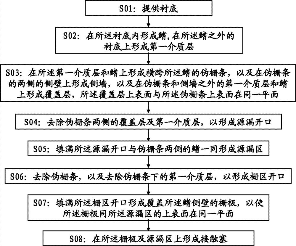
为了解决鳍式场效应晶体管制造中接触塞对准不精确的问题,本发明提供了一种鳍式场效应晶体管的制造方法,参考图2,图2示出了本发明鳍式场效应晶体管制造方法的流程图,以下结合图3-图31对本发明的制造方法进行详细说明,实施例中例举的方法为优选方案,是为了更好的说明和理解本发明,而不是限制本发明。In order to solve the problem of inaccurate alignment of contact plugs in the manufacture of Fin Field Effect Transistors, the present invention provides a method for manufacturing Fin Field Effect Transistors. Referring to FIG. 2, FIG. The flow chart of the method, the manufacturing method of the present invention will be described in detail below with reference to Fig. 3-Fig.
在步骤S01,提供衬底200。In step S01, a
如图3所示,在本实施例中,所述衬底为SOI衬底200,SOI衬底200包括背衬底200a、埋氧层200b和顶层硅200c。在其他实施例中,所述衬底还可以为包括半导体层和绝缘层的衬底结构。As shown in FIG. 3, in this embodiment, the substrate is an
在步骤S02,在所述衬底200内形成鳍202,以及在所述鳍202之外的衬底上形成第一介质层206,参考图4(俯视图)和图5(图4的AA’向视图)。In step S02,
具体地,首先,可以在顶层硅200c上形成帽层204,而后图形化所述帽层204,并以帽层204为硬掩膜,利用刻蚀技术,例如RIE(反应离子刻蚀)的方法,刻蚀顶层硅200c,从而在顶层硅200c内形成鳍202,可选地,可以进一步去除帽层204,或者保留帽层204,以保护鳍在后续工艺中不受其他工艺的影响。而后,淀积介质材料,例如SiO2,并进行平坦化,例如CMP(化学机械研磨),从而在所述鳍202之外的衬底200b上形成第一介质层206,所述第一介质层的上表面与鳍的上表面齐平。Specifically, first, a
在步骤S03,在所述第一介质层206和鳍202上形成横跨所述鳍202的伪栅条208,以及在伪栅条208的两侧的侧壁上形成侧墙210,以及在伪栅条208和侧墙210之外的第一介质层206和鳍202上形成覆盖层212、214,所述覆盖层212、214上表面与所述伪栅条208上表面在同一平面,参考图6(俯视图)、图7(图6的AA’向视图)、图8(图6的BB’向视图)。In step S03, a
具体地,首先,在上述器件上淀积伪栅条,例如多晶硅,并进行图案化,形成横跨所述鳍202的伪栅条208,而后,淀积侧墙,例如Si3N4,通过刻蚀在伪栅条208的侧壁上形成侧墙210。所述伪栅条208和侧墙210可以作为后续工艺中的掩膜图案层,以及便于后续工艺自对准形成源漏区及栅极。Specifically, firstly, dummy gate strips, such as polysilicon, are deposited on the above device and patterned to form dummy gate strips 208 across the
而后,形成覆盖层,所述覆盖层可以为一层或多层结构,在本实施例中,优选覆盖层为包括第二介质层和第三介质层的两层结构,优选地,所述第三介质层、第二介质层及侧墙采用互不相同的介质材料,方便于后续工艺自对准形成源漏区及栅极,简化工艺。在本实施例中,可以通过淀积第二介质层,例如SiO2,以及第三介质层,例如高k介质材料(如HfO2),而后,进行平坦化,例如CMP(化学机械研磨)的方法,以伪栅条208为停止层。Then, a cover layer is formed, and the cover layer may have a one-layer or multi-layer structure. In this embodiment, the cover layer is preferably a two-layer structure including a second dielectric layer and a third dielectric layer. Preferably, the first The three dielectric layers, the second dielectric layer and the side walls are made of different dielectric materials, which facilitates the self-alignment of the source-drain region and the gate in the subsequent process and simplifies the process. In this embodiment, a second dielectric layer, such as SiO 2 , and a third dielectric layer, such as a high-k dielectric material (such as HfO 2 ), can be deposited, and then planarized, such as CMP (Chemical Mechanical Polishing) In this method, the
从而,在去除帽层的实施例中,在伪栅条208和侧墙210之外的第一介质层206和鳍202上形成覆盖层212、214,或者,在未去除帽层的实施例中,在所述第一介质206层和帽层204上形成横跨所述鳍的伪栅条208,以及在伪栅条208的两侧的侧壁上形成侧墙210,以及在伪栅条208和侧墙210之外的第一介质层206和帽层204上形成覆盖层212、214,所述覆盖层212、214上表面与所述伪栅条208上表面在同一平面。Therefore, in an embodiment in which the capping layer is removed, covering
在步骤S04,去除伪栅条208两侧的覆盖层212、214及第一介质层206,以形成源漏开口216,所述源漏开口216暴露伪栅条208两侧的鳍202,参考图9(俯视图)、图10(图9的AA’向视图)、图11(图9的BB’向视图)和图12(图9的CC’向视图)。In step S04, the cover layers 212, 214 and the
可以利用刻蚀技术,例如RIE的方法,去除伪栅条208两侧的覆盖层212、214及第一介质层206,并停止在鳍202上,充分暴露伪栅条208两侧的鳍202,从而形成源漏开口216。The covering layers 212, 214 and the
在未去除帽层204的实施例中,可以进一步的去除伪栅条208两侧的鳍202上的帽层204,以充分暴露伪栅条208两侧的鳍202。In an embodiment where the
在步骤S05,填满所述源漏开口216与伪栅条208两侧的鳍202一同形成源漏区218,参考图13(俯视图)、图14(图13的AA’向视图)、图15(图13的BB’向视图)和图16(图13的CC’向视图)。In step S05, fill the source and drain
本实施例中,可以通过外延生长(epi)的方法,在伪栅条208两侧的鳍202上外延生长外延层来填满所述源漏开口216,例如,对于NFET为SiC,对于PFET为SiGe,并进行CMP,以伪栅条208为停止层,该外延层同伪栅条208两侧的鳍202一同形成源漏区218,在本实施例中,由于外延层会向伪栅条208两侧的鳍202扩散,使伪栅条208两侧的鳍202部分或全部转变为外延层的材料(图示为全部转变为外延层材料)。在其他实施例中,还可以采用其他合适的方法形成该源漏区218。In this embodiment, the epitaxial growth (epi) method can be used to epitaxially grow epitaxial layers on the
在步骤S06,去除伪栅条208,以及去除伪栅条208下的第一介质层206,以形成栅区开口220,所述栅区开口220暴露伪栅条208下的鳍202,参考图17(俯视图)、图18(图17的AA’向视图)、图19(图17的BB’向视图)和图20(图17的CC’向视图)。In step S06, the
通过湿法或干法刻蚀技术,去除伪栅条208,以及进一步去除伪栅条208下的第一介质层206,充分暴露伪栅条208下面的鳍202或帽层204,形成栅区开口220。By wet or dry etching technology, remove the
在步骤S07,填满所述栅区开口220形成覆盖所述鳍202的栅极,以使所述栅极同所述源漏区218的上表面在同一平面,参考图21(俯视图)、图22(图21的AA’向视图)和图23(图21的BB’向视图),其中栅极包括栅介质层222和栅电极224、226。In step S07, the gate region opening 220 is filled to form a gate covering the
具体地,可以首先形成覆盖所述栅区开口220中的鳍202的栅介质层222,所述栅介质层222可以为一层或多层结构,一层结构的一些实施例中,栅介质层222可以为高k介质材料(例如,和氧化硅相比,具有高介电常数的材料)或其他栅介质材料,多层结构的一些实施例中,栅介质层222可以包括界面层和高k介质材料,所述界面层可以为氧化硅、氮化硅、氮氧化硅或其他材料,高k介质材料例如铪基氧化物,HFO2、HfSiO、HfSiON、HfTaO、HfTiO等,此处仅为示例,本发明不限于此。Specifically, the
而后在栅介质层222上形成栅电极,所述栅电极可以为一层或多层结构,栅电极可以包括金属栅电极或多晶硅,例如可以包括:Ti、TiAlx、TiN、TaNx、HfN、TiCx、TaCx、HfCx、Ru、TaNx、TiAlN、WCN、MoAlN、RuOx、多晶硅或其他合适的材料,或他们的组合。在本实施例中,所述栅电极为两层结构,包括金属栅224和多晶硅层226,可以通过淀积金属栅,例如NFET为TiN,PFET为TiCx,而后通过刻蚀,仅在鳍202的侧壁的栅介质层222上形成金属栅224,而后填充多晶硅,并进行CMP,从而在栅区开口220中形成覆盖所述鳍202的栅极,其中栅极包括栅介质层222、金属栅224和多晶硅层226,所述栅极同源漏区218的上表面在同一平面。Then a gate electrode is formed on the
至此,形成了多个栅极、源漏区相连接的鳍式场效应晶体管器件,而后,根据需要,可选地,可以进一步形成隔离区,将其分隔成绝缘的多个器件。如图24(俯视图)、图25(图24的AA’向视图)、图26(图24的BB’向视图)和图27(图24的CC’向视图)所示,首先刻蚀去除鳍202之间的部分栅极以及部分源漏区218,形成栅隔离开口230和源漏隔离开口228,可选地,形成栅隔离开口230时,可以仅去除栅电极224、226,而不去除栅介质层222,以简化工艺,优选地,栅隔离开口230和源漏隔离开口228去除的部分可以不对准,即开口的边缘不在一条直线上,从而,所述栅极226的边沿与所述源漏区218的边沿不在一条直线上,这样在后续形成接触时,更利于栅极、源漏区的接触分别对准到栅极、源漏区。而后,填充栅隔离开口230和源漏隔离开口228形成栅隔离区234以及源漏隔离区232,参考图28(俯视图)、图29(图28的AA’向视图)、图30(图28的BB’向视图)和图31(图28的CC’向视图)。So far, a plurality of fin field effect transistor devices with gates and source-drain regions connected have been formed, and then, optionally, isolation regions can be further formed to separate them into a plurality of isolated devices as required. As shown in Figure 24 (top view), Figure 25 (A-A' view in Figure 24), Figure 26 (BB' view in Figure 24) and Figure 27 (CC' view in Figure 24), first etch to remove the fins Part of the gate between 202 and part of the source-
在步骤S08,在所述栅极及源漏区218上形成接触塞238,参考图28(俯视图)、图29(图28的AA’向视图)、图30(图28的BB’向视图)和图31(图28的CC’向视图)。In step S08, contact plugs 238 are formed on the gate and source/
具体地,在本实施例中,可以通过,首先淀积第四介质层236,优选地,该介质层236可以同上述填充栅隔离开口230和源漏隔离开口228的步骤一起进行,并进行平坦化,同时形成栅隔离区234、源漏隔离区232以及第四介质层236。Specifically, in this embodiment, the
而后,刻蚀所述第四介质层236在栅极和源漏区218上形成接触孔,而后,填充金属材料,例如W等,从而形成接触塞238。而由于栅极和源漏区218在一个平面上,相比较栅极和源漏区不等高鳍式器件,更容易对准,并且栅极和源漏区之间由侧墙210隔开,更易对准。Then, the
以上对本发明的鳍式场效应晶体管的制造方法进行了详细的描述,以上所述,仅是本发明的较佳实施例而已,并非对本发明作任何形式上的限制。The manufacturing method of the fin field effect transistor of the present invention has been described in detail above, and the above description is only a preferred embodiment of the present invention, and does not limit the present invention in any form.
同时,本发明还提出了根据上述方法形成的鳍式场效应晶体管结构,参考图28-31,所述结构包括:At the same time, the present invention also proposes a fin field effect transistor structure formed according to the above method, referring to FIGS. 28-31 , the structure includes:
衬底200a、200b;
衬底上的鳍202,所述鳍202具有相对的第一端202-1和第二端202-2,以及相对的第三端202-3和第四端202-4;a
覆盖所述鳍第一端202-1、第二端202-2表面以及上表面202-5的栅极;A grid covering the surfaces of the first end 202-1, the second end 202-2 and the upper surface 202-5 of the fin;
位于所述鳍第三端202-3和第四端202-4两侧的源漏区218,其中源漏区218和栅极的上表面在同一平面;The source and drain
位于所述鳍上表面202-5之上的栅极同源漏区218之间的侧墙210;The
栅极及源漏区218上的接触塞238。Contact plugs 238 on the gate and source and drain
在本实施例中,所述衬底包括多晶硅层200a和其上的绝缘层200b,所述衬底还可以是其他结构。In this embodiment, the substrate includes a
在本实施例中,所述栅极包括栅介质层222、金属栅224和多晶硅层226,所述栅极还可以是其他结构。In this embodiment, the gate includes a
此外,所述晶体管还可以包括:相邻源漏区218之间的源漏隔离区232,以及相邻栅极之间的栅隔离区234。In addition, the transistor may further include: a source-
此外,优选地,沿鳍第三端202-3与第四端202-4连线的方向上,所述栅极的边沿与所述源漏区218的边沿不在一条直线上。In addition, preferably, along the direction connecting the third terminal 202 - 3 and the fourth terminal 202 - 4 of the fin, the edge of the gate and the edge of the source and drain
虽然本发明已以较佳实施例披露如上,然而并非用以限定本发明。任何熟悉本领域的技术人员,在不脱离本发明技术方案范围情况下,都可利用上述揭示的方法和技术内容对本发明技术方案作出许多可能的变动和修饰,或修改为等同变化的等效实施例。因此,凡是未脱离本发明技术方案的内容,依据本发明的技术实质对以上实施例所做的任何简单修改、等同变化及修饰,均仍属于本发明技术方案保护的范围内。Although the present invention has been disclosed above with preferred embodiments, it is not intended to limit the present invention. Any person familiar with the art, without departing from the scope of the technical solution of the present invention, can use the methods and technical content disclosed above to make many possible changes and modifications to the technical solution of the present invention, or modify it into an equivalent implementation of equivalent changes example. Therefore, any simple modifications, equivalent changes and modifications made to the above embodiments according to the technical essence of the present invention, which do not deviate from the technical solution of the present invention, still fall within the protection scope of the technical solution of the present invention.
Claims (11)
Priority Applications (3)
| Application Number | Priority Date | Filing Date | Title |
|---|---|---|---|
| CN201110116545.5A CN102768957B (en) | 2011-05-06 | 2011-05-06 | Fin field effect transistor and manufacturing method thereof |
| PCT/CN2011/078207 WO2012151797A1 (en) | 2011-05-06 | 2011-08-10 | Fin field effect transistor and manufacture method thereof |
| US13/377,141 US8859378B2 (en) | 2011-05-06 | 2011-08-10 | Fin field-effect transistor and method for manufacturing the same |
Applications Claiming Priority (1)
| Application Number | Priority Date | Filing Date | Title |
|---|---|---|---|
| CN201110116545.5A CN102768957B (en) | 2011-05-06 | 2011-05-06 | Fin field effect transistor and manufacturing method thereof |
Publications (2)
| Publication Number | Publication Date |
|---|---|
| CN102768957A true CN102768957A (en) | 2012-11-07 |
| CN102768957B CN102768957B (en) | 2016-09-14 |
Family
ID=47096310
Family Applications (1)
| Application Number | Title | Priority Date | Filing Date |
|---|---|---|---|
| CN201110116545.5A Active CN102768957B (en) | 2011-05-06 | 2011-05-06 | Fin field effect transistor and manufacturing method thereof |
Country Status (3)
| Country | Link |
|---|---|
| US (1) | US8859378B2 (en) |
| CN (1) | CN102768957B (en) |
| WO (1) | WO2012151797A1 (en) |
Cited By (15)
| Publication number | Priority date | Publication date | Assignee | Title |
|---|---|---|---|---|
| WO2014036677A1 (en) * | 2012-09-10 | 2014-03-13 | 中国科学院微电子研究所 | Semiconductor device and manufacturing method therefor |
| CN103839820A (en) * | 2012-11-25 | 2014-06-04 | 中国科学院微电子研究所 | Semiconductor device manufacturing method |
| CN103839819A (en) * | 2012-11-25 | 2014-06-04 | 中国科学院微电子研究所 | Semiconductor device and manufacturing method thereof |
| CN103855009A (en) * | 2012-11-30 | 2014-06-11 | 中国科学院微电子研究所 | Fin structure manufacturing method |
| WO2014166146A1 (en) * | 2013-04-08 | 2014-10-16 | 中国科学院微电子研究所 | Finfet and manufacturing method for same |
| CN104681563A (en) * | 2013-11-28 | 2015-06-03 | 中国科学院微电子研究所 | Semiconductor device and manufacturing method thereof |
| CN105826382A (en) * | 2015-01-09 | 2016-08-03 | 中国科学院微电子研究所 | Semiconductor device manufacturing method |
| CN108074871A (en) * | 2016-11-11 | 2018-05-25 | 中芯国际集成电路制造(上海)有限公司 | Dynamic RAM and forming method thereof |
| CN108269803A (en) * | 2016-12-30 | 2018-07-10 | 台湾积体电路制造股份有限公司 | Semiconductor devices and its manufacturing method |
| CN109920738A (en) * | 2019-03-08 | 2019-06-21 | 中国科学院微电子研究所 | Semiconductor structure and its production method |
| CN110571188A (en) * | 2018-06-05 | 2019-12-13 | 中芯国际集成电路制造(上海)有限公司 | Contact plug, semiconductor device and manufacturing method thereof |
| CN112542506A (en) * | 2019-09-23 | 2021-03-23 | 中芯国际集成电路制造(上海)有限公司 | Semiconductor device and method of forming the same |
| CN112582471A (en) * | 2019-09-29 | 2021-03-30 | 中芯国际集成电路制造(上海)有限公司 | Semiconductor device and forming method |
| CN113066725A (en) * | 2021-03-17 | 2021-07-02 | 泉芯集成电路制造(济南)有限公司 | A transistor and method of making the same |
| WO2022241667A1 (en) * | 2021-05-19 | 2022-11-24 | 中芯国际集成电路制造(上海)有限公司 | Semiconductor structure, forming method therefor, and working method thereof |
Families Citing this family (17)
| Publication number | Priority date | Publication date | Assignee | Title |
|---|---|---|---|---|
| US8981496B2 (en) * | 2013-02-27 | 2015-03-17 | Taiwan Semiconductor Manufacturing Company, Ltd. | Metal gate and gate contact structure for FinFET |
| US9711374B2 (en) * | 2013-06-13 | 2017-07-18 | Taiwan Semiconductor Manufacturing Co., Ltd. | Mechanisms for forming oxide layer over exposed polysilicon during a chemical mechanical polishing (CMP) process |
| US9590104B2 (en) | 2013-10-25 | 2017-03-07 | Taiwan Semiconductor Manufacturing Company, Ltd. | Gate device over strained fin structure |
| US9299781B2 (en) | 2014-04-01 | 2016-03-29 | Globalfoundries Inc. | Semiconductor devices with contact structures and a gate structure positioned in trenches formed in a layer of material |
| US9171934B2 (en) * | 2014-04-01 | 2015-10-27 | Globalfoundries Inc. | Methods of forming semiconductor devices using a layer of material having a plurality of trenches formed therein |
| US9659827B2 (en) | 2014-07-21 | 2017-05-23 | Samsung Electronics Co., Ltd. | Methods of manufacturing semiconductor devices by forming source/drain regions before gate electrode separation |
| EP3198652A4 (en) | 2014-09-26 | 2018-05-30 | INTEL Corporation | Selective gate spacers for semiconductor devices |
| US9443738B2 (en) * | 2015-02-06 | 2016-09-13 | Globalfoundries Inc. | Integrated circuits with middle of line capacitance reduction in self-aligned contact process flow and fabrication methods |
| KR102270916B1 (en) | 2015-04-06 | 2021-06-29 | 삼성전자주식회사 | Semiconductor device and method of fabricating the same |
| US10441189B2 (en) * | 2015-12-15 | 2019-10-15 | International Business Machines Corporation | High definition EEG |
| US9768072B1 (en) | 2016-06-30 | 2017-09-19 | International Business Machines Corporation | Fabrication of a vertical fin field effect transistor with reduced dimensional variations |
| US10950606B2 (en) | 2016-09-30 | 2021-03-16 | Intel Corporation | Dual fin endcap for self-aligned gate edge (SAGE) architectures |
| US10629706B2 (en) * | 2018-05-10 | 2020-04-21 | Taiwan Semiconductor Manufacturing Co., Ltd. | Fin and gate dimensions for optimizing gate formation |
| KR102520599B1 (en) * | 2018-07-23 | 2023-04-11 | 삼성전자주식회사 | A semiconductor device |
| CN113540019B (en) * | 2020-04-20 | 2023-07-21 | 中芯国际集成电路制造(上海)有限公司 | Variable capacitor and method for forming variable capacitor |
| CN116072713A (en) * | 2021-11-03 | 2023-05-05 | 中芯南方集成电路制造有限公司 | Semiconductor structures and methods of forming them |
| US12237232B2 (en) * | 2022-02-08 | 2025-02-25 | Taiwan Semiconductor Manufacturing Company, Ltd. | Methods for forming source/drain features |
Citations (5)
| Publication number | Priority date | Publication date | Assignee | Title |
|---|---|---|---|---|
| US6252284B1 (en) * | 1999-12-09 | 2001-06-26 | International Business Machines Corporation | Planarized silicon fin device |
| US20050199920A1 (en) * | 2004-03-11 | 2005-09-15 | Deok-Hyung Lee | Fin field effect transistors with low resistance contact structures and methods of manufacturing the same |
| CN1893079A (en) * | 2005-06-28 | 2007-01-10 | 三星电子株式会社 | CMOS device, method of manufacturing the same, and memory including cmos device |
| US20090020764A1 (en) * | 2007-07-16 | 2009-01-22 | Anderson Brent A | Graphene-based transistor |
| CN102034831A (en) * | 2009-09-28 | 2011-04-27 | 中芯国际集成电路制造(上海)有限公司 | Circle stacking grid fin type field-effect transistor memory device and forming method thereof |
Family Cites Families (8)
| Publication number | Priority date | Publication date | Assignee | Title |
|---|---|---|---|---|
| JP2005086024A (en) | 2003-09-09 | 2005-03-31 | Toshiba Corp | Semiconductor device and method for manufacturing same |
| US8264048B2 (en) * | 2008-02-15 | 2012-09-11 | Intel Corporation | Multi-gate device having a T-shaped gate structure |
| US8637359B2 (en) * | 2011-06-10 | 2014-01-28 | International Business Machines Corporation | Fin-last replacement metal gate FinFET process |
| US20130075818A1 (en) * | 2011-09-23 | 2013-03-28 | Taiwan Semiconductor Manufacturing Company, Ltd. | 3D Semiconductor Device and Method of Manufacturing Same |
| US20130175579A1 (en) * | 2012-01-10 | 2013-07-11 | International Business Machines Corporation | Transistor with recessed channel and raised source/drain |
| US9698229B2 (en) * | 2012-01-17 | 2017-07-04 | United Microelectronics Corp. | Semiconductor structure and process thereof |
| US8637371B2 (en) * | 2012-02-16 | 2014-01-28 | International Business Machines Corporation | Non-planar MOSFET structures with asymmetric recessed source drains and methods for making the same |
| US20130270638A1 (en) * | 2012-04-13 | 2013-10-17 | International Business Machines Corporation | Strained soi finfet on epitaxially grown box |
-
2011
- 2011-05-06 CN CN201110116545.5A patent/CN102768957B/en active Active
- 2011-08-10 WO PCT/CN2011/078207 patent/WO2012151797A1/en not_active Ceased
- 2011-08-10 US US13/377,141 patent/US8859378B2/en active Active
Patent Citations (5)
| Publication number | Priority date | Publication date | Assignee | Title |
|---|---|---|---|---|
| US6252284B1 (en) * | 1999-12-09 | 2001-06-26 | International Business Machines Corporation | Planarized silicon fin device |
| US20050199920A1 (en) * | 2004-03-11 | 2005-09-15 | Deok-Hyung Lee | Fin field effect transistors with low resistance contact structures and methods of manufacturing the same |
| CN1893079A (en) * | 2005-06-28 | 2007-01-10 | 三星电子株式会社 | CMOS device, method of manufacturing the same, and memory including cmos device |
| US20090020764A1 (en) * | 2007-07-16 | 2009-01-22 | Anderson Brent A | Graphene-based transistor |
| CN102034831A (en) * | 2009-09-28 | 2011-04-27 | 中芯国际集成电路制造(上海)有限公司 | Circle stacking grid fin type field-effect transistor memory device and forming method thereof |
Cited By (22)
| Publication number | Priority date | Publication date | Assignee | Title |
|---|---|---|---|---|
| WO2014036677A1 (en) * | 2012-09-10 | 2014-03-13 | 中国科学院微电子研究所 | Semiconductor device and manufacturing method therefor |
| CN103839820A (en) * | 2012-11-25 | 2014-06-04 | 中国科学院微电子研究所 | Semiconductor device manufacturing method |
| CN103839819A (en) * | 2012-11-25 | 2014-06-04 | 中国科学院微电子研究所 | Semiconductor device and manufacturing method thereof |
| CN103839820B (en) * | 2012-11-25 | 2018-07-31 | 中国科学院微电子研究所 | Semiconductor device manufacturing method |
| CN103855009A (en) * | 2012-11-30 | 2014-06-11 | 中国科学院微电子研究所 | Fin structure manufacturing method |
| US9419112B2 (en) | 2012-11-30 | 2016-08-16 | Institute of Microelectronics, Chinese Academy of Sciences | Method for manufacturing fin structure |
| WO2014166146A1 (en) * | 2013-04-08 | 2014-10-16 | 中国科学院微电子研究所 | Finfet and manufacturing method for same |
| CN104681563A (en) * | 2013-11-28 | 2015-06-03 | 中国科学院微电子研究所 | Semiconductor device and manufacturing method thereof |
| CN104681563B (en) * | 2013-11-28 | 2018-05-08 | 中国科学院微电子研究所 | Semiconductor device and manufacturing method thereof |
| CN105826382A (en) * | 2015-01-09 | 2016-08-03 | 中国科学院微电子研究所 | Semiconductor device manufacturing method |
| CN108074871B (en) * | 2016-11-11 | 2020-06-09 | 中芯国际集成电路制造(上海)有限公司 | Dynamic random access memory and forming method thereof |
| CN108074871A (en) * | 2016-11-11 | 2018-05-25 | 中芯国际集成电路制造(上海)有限公司 | Dynamic RAM and forming method thereof |
| CN108269803A (en) * | 2016-12-30 | 2018-07-10 | 台湾积体电路制造股份有限公司 | Semiconductor devices and its manufacturing method |
| CN108269803B (en) * | 2016-12-30 | 2021-03-30 | 台湾积体电路制造股份有限公司 | Semiconductor device and method of manufacturing the same |
| CN110571188A (en) * | 2018-06-05 | 2019-12-13 | 中芯国际集成电路制造(上海)有限公司 | Contact plug, semiconductor device and manufacturing method thereof |
| CN109920738A (en) * | 2019-03-08 | 2019-06-21 | 中国科学院微电子研究所 | Semiconductor structure and its production method |
| CN112542506A (en) * | 2019-09-23 | 2021-03-23 | 中芯国际集成电路制造(上海)有限公司 | Semiconductor device and method of forming the same |
| CN112542506B (en) * | 2019-09-23 | 2025-07-01 | 中芯国际集成电路制造(上海)有限公司 | Semiconductor device and method for forming the same |
| CN112582471A (en) * | 2019-09-29 | 2021-03-30 | 中芯国际集成电路制造(上海)有限公司 | Semiconductor device and forming method |
| CN113066725A (en) * | 2021-03-17 | 2021-07-02 | 泉芯集成电路制造(济南)有限公司 | A transistor and method of making the same |
| CN113066725B (en) * | 2021-03-17 | 2023-03-28 | 泉芯集成电路制造(济南)有限公司 | Transistor and manufacturing method thereof |
| WO2022241667A1 (en) * | 2021-05-19 | 2022-11-24 | 中芯国际集成电路制造(上海)有限公司 | Semiconductor structure, forming method therefor, and working method thereof |
Also Published As
| Publication number | Publication date |
|---|---|
| US8859378B2 (en) | 2014-10-14 |
| CN102768957B (en) | 2016-09-14 |
| WO2012151797A1 (en) | 2012-11-15 |
| US20120286337A1 (en) | 2012-11-15 |
Similar Documents
| Publication | Publication Date | Title |
|---|---|---|
| CN102768957B (en) | Fin field effect transistor and manufacturing method thereof | |
| CN112309860B (en) | Semiconductor structures and methods of forming them | |
| CN102810476B (en) | Fin field effect transistor manufacturing method | |
| US9281378B2 (en) | Fin recess last process for FinFET fabrication | |
| CN110517989A (en) | Semiconductor structure and forming method thereof | |
| US20130052778A1 (en) | Semiconductor process | |
| CN106252391B (en) | Semiconductor structure and manufacturing method thereof | |
| CN107230728A (en) | Semiconductor devices, FINFET device and forming method thereof | |
| US9076870B2 (en) | Method for forming fin-shaped structure | |
| CN111106064B (en) | Semiconductor structure and method of forming the same | |
| CN102543745B (en) | Method of forming semiconductor device | |
| CN105336624B (en) | Fin field effect transistor and method for manufacturing the dummy gate | |
| CN104681563A (en) | Semiconductor device and manufacturing method thereof | |
| CN103295903B (en) | Method for manufacturing fin-type semiconductor device with gate-surrounding structure | |
| CN104124160B (en) | Semiconductor device manufacturing method | |
| CN104241360B (en) | Semiconductor device and method for fabricating the same | |
| US9773911B2 (en) | Fin field effect transistor and fabricating method thereof | |
| CN103681840B (en) | Semiconductor device and manufacturing method thereof | |
| CN116072676A (en) | Semiconductor structures and methods of forming them | |
| CN115116948A (en) | Method of forming a semiconductor structure | |
| CN103311280B (en) | Semiconductor device and manufacturing method thereof | |
| CN105845726A (en) | All-around gate field-effect transistor and manufacturing method thereof | |
| TW201448120A (en) | Semiconductor device and fabrication method thereof | |
| CN110875390A (en) | Semiconductor structure and method of forming the same | |
| CN117438426A (en) | Semiconductor structure and forming method thereof |
Legal Events
| Date | Code | Title | Description |
|---|---|---|---|
| C06 | Publication | ||
| PB01 | Publication | ||
| C10 | Entry into substantive examination | ||
| SE01 | Entry into force of request for substantive examination | ||
| C14 | Grant of patent or utility model | ||
| GR01 | Patent grant |