Description of drawings
Element circuit (1) has two kinds of circuit forms:
The field effect transistor Q1 of element circuit (1.1) is the N raceway groove, and field effect transistor Q2 is the P raceway groove; The positive pole of diode D1 is connected with the negative pole of diode D2, consist of terminal A, the drain electrode of field effect transistor Q1 is connected with the negative pole of diode D1, its source electrode connects terminal B, and the drain electrode of field effect transistor Q2 is connected with the positive pole of diode D2, and its source electrode connects terminal B, the grid of field effect transistor Q1 connects the positive pole that drives signal V1, the negative pole that drives signal V1 connects terminal B, and the grid of field effect transistor Q2 connects the negative pole that drives signal V2, and the positive pole that drives signal V2 connects terminal B;
The field effect transistor Q1 of element circuit (1.2) is the N raceway groove, field effect transistor Q2 is the P raceway groove, the drain electrode of field effect transistor Q1 is terminal A, the source electrode of field effect transistor Q2 is terminal B, the source electrode of field effect transistor Q1 connects the drain electrode of field effect transistor Q2, the grid of field effect transistor Q1 connects the grid of field effect transistor Q2, connects simultaneously the positive pole of driving voltage V, and the negative pole of driving voltage V connects terminal B.
Basic circuit (2) has three kinds of circuit forms:
Basic circuit (2.1) is comprised of element circuit (1) and resistance R 1, the terminal A of element circuit (1) connects the live wire of input voltage vin, resistance R 1 is connected between the terminal B of the zero line of input voltage vin and element circuit (1), and the terminal B of element circuit (1) is exactly the output of basic circuit (2.1); Can also connect boost capacitor network (UPnet) and decompression capacitor network (DNnet) between the terminal B of element circuit (1) and ground, replace resistance R 1;
Basic circuit (2.2) is comprised of element circuit (1) and transformer TX1 etc., the terminal A of element circuit (1) connects the elementary different name end of transformer TX1, the positive pole of its termination input voltage vin of the same name or live wire, the terminal B of element circuit (1) connects negative pole or the zero line of input voltage vin, at pair edge joint active rectification circuit (3) of transformer;
Basic circuit (2.3) is comprised of element circuit (1), resistance R 1 and transformer TX1 etc., the terminal A of element circuit (1) connects the elementary different name end of transformer TX1, the positive pole of its termination input voltage vin of the same name or live wire, the end of the terminal B connecting resistance R2 of element circuit (1), the other end of the negative pole of input voltage vin or zero line connecting resistance R2, the terminal B of element circuit (1) is exactly the output of basic circuit (2.3); Transformer TX1 pay edge joint active rectification circuit (3), can also connect boost capacitor network (UPnet) and decompression capacitor network (DNnet), replacement resistance R 2 between the terminal B of element circuit (1) and ground.
Driving signal V1, V2 are produced by high-frequency driving signal generator (VDrvh) and synchronized signal generator (VDrvs):
high-frequency driving signal generator (VDrvh) is comprised of integrated circuit NE555 and signal conversion circuit (SPrs), DC power supply V3, the V4 series connection, middle ground, the negative pole of direct voltage V3 meets the pin GND of NE555, capacitor C 1, the end of C2, the positive pole of direct voltage V4 meets the pin Vcc of NE555, Reset, one end of resistance R 7, the pin Thresh of another termination NE555 of capacitor C 1, the pin Cntrl of another termination NE555 of capacitor C 2, the pin Dis of another termination NE555 of resistance, the positive pole of diode D1 meets the pin Dis of NE555, its negative pole meets the pin Trig of NE555, diode D2 and resistance R 6 series connection, the positive pole of diode D2 meets the pin Thresh of NE555, the pin Dis of another termination NE555 of diode D6, the pin Out of NE555 meets the end points IN of signal conversion circuit SPrs by resistance R 3, the end points GND ground connection of signal conversion circuit SPrs,
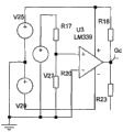
synchronized signal generator (VDrvs) is comprised of integrated circuit LM339 and signal conversion circuit (SPrs), DC power supply V4, the V5 series connection, middle ground, the negative pole of direct voltage V4 connect the supply pin of LM339-, the positive pole of direct voltage V5 connects the supply pin of LM339+and end of resistance R 8, the exit point Gc of another termination LM339 of resistance R 8, one end ground connection of the negative pole of power supply V3 and resistance R 6, the homophase input pin of another termination LM339 of resistance R 6+, the positive pole of power supply V3 by resistance R 7 connect the homophase input pin of LM339+, anti-phase input pin-ground connection of LM339, the exit point Gc of LM339 meets the end points IN of signal conversion circuit SPrs by resistance R 3, the end points GND ground connection of signal conversion circuit (SPrs),
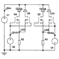
Signal conversion circuit (SPrs) is comprised of optocoupler U1, U2 etc., the negative electrode of the diode part of optocoupler U1 meets input endpoint IN, its anode meets end points GND, the emitter of the triode part of optocoupler U1 connects the negative pole of power supply V2 by resistance, connect simultaneously the collector electrode of triode Q2, the collector electrode of the triode part of optocoupler U1 connects the positive pole of power supply V1, connect simultaneously the collector electrode of triode Q1,, triode Q1, Q2 emitter be connected together and consist of exit point Gb, meet end points GND by resistance R 2 simultaneously; The anode of the diode part of optocoupler U2 meets input endpoint IN, its negative electrode meets end points GND, the emitter of the triode part of optocoupler U2 connects the negative pole of power supply V2 by resistance, connect simultaneously the collector electrode of triode Q4, the collector electrode of the triode part of optocoupler U2 connects the positive pole of power supply V1, connect simultaneously the collector electrode of triode Q3,, the emitter of triode Q3, Q4 is connected together and consists of exit point Ga, meets end points GND by resistance R 5 simultaneously.
Active rectification circuit (3) has four kinds of circuit forms:
Active rectification circuit (3.1) is made of element circuit (1.1) and two resistance, the source electrode of two field effect transistor Q1, Q2 of element circuit (1.1) separately, the end of the source electrode connecting resistance R1 of field effect transistor Q1, consist of exit point P+, the end of the source electrode connecting resistance R2 of field effect transistor Q2, consist of exit point N-,, another termination exit point N of resistance R 1, R2, the terminal A of element circuit (1.1) consists of input endpoint L;
Active rectification circuit (3.2) is made of element circuit (1.1) and a resistance, the terminal A of one termination unit circuit (1.1) of resistance R 1, consist of exit point P+, its other end consists of exit point N-and input endpoint N, and element circuit 1.1 terminal A consist of input endpoint L;
Active rectification circuit (3.3) is made of two element circuits (1.2) and two resistance, the terminal A of two element circuits (1.2) is connected together and consists of input endpoint L, the end of the terminal B connecting resistance R1 of first module circuit (1.2), consist of exit point P+, the end of the terminal B connecting resistance R2 of second unit circuit 1.2, consist of exit point N-,, the other end of resistance R 1, R2 consists of input endpoint N;
Active rectification circuit (3.4) is comprised of four element circuits (1.2), the first, the terminal A of the 3rd element circuit (1.2) is connected together, consist of exit point P+, the second, the terminal B of the 4th element circuit (1.2) is connected together, consist of exit point N-, the terminal A of the terminal B of first module circuit (1.2) and the 4th element circuit (1.2) is connected together, consist of input endpoint L, the terminal A of the terminal B of the 3rd element circuit (1.2) and second unit circuit (1.2) is connected together, and consists of input endpoint N.
Panel height modulation circuit (4) is comprised of 30 integrated circuits:
the homophase termination commutating voltage Vd of integrated circuit U3, end of oppisite phase connecting resistance R3 and resistance R 10, output connects the positive pole of direct voltage V3 by resistance R 4, connect simultaneously the terminal B of integrated circuit U4, the positive pole of another termination voltage V3 of resistance R 3, the other end ground connection of resistance R 10, capacitor C 4 is also in parallel through voltage V3, exchange the live wire that detects voltage V1 and connect the anode of diode D1 and the negative electrode of diode D3, its zero line connects the anode of diode D2 and the negative electrode of diode D4, , diode D1, the negative electrode of D2 is the end of connecting resistance R2 simultaneously, , diode D3, D4 is the end of connecting resistance R11 simultaneously, , resistance R 2, R11 connects the terminal B of integrated circuit U3 simultaneously, the terminal A of integrated circuit U4 is by resistance R 12 ground connection, and end points RST connects the positive pole of direct voltage V3 by resistance R 5, and end points CRext meets end points Cext by capacitor C 1, connects the positive pole of voltage V3 by resistance, and end points QP connects, the end of integrated circuit U5, U9,
The homophase termination commutating voltage Vd of two integrated circuit U12, the positive pole of anti-phase termination voltage V2, output connect the positive pole of voltage V3 by resistance R 20, connect simultaneously the terminal B of integrated circuit U13; The terminal A of integrated circuit U13 is by resistance R 26 ground connection, end points RST connects the positive pole of voltage V3 by resistance R 21, end points CRext meets end points Cext by capacitor C 2, connects the positive pole of voltage V3 by resistance R 17, end points QP connects the other end of integrated circuit, connects simultaneously the output of integrated circuit U29;
The homophase termination commutating voltage Vd of integrated circuit U19, the positive pole of anti-phase termination voltage V29, output connect the positive pole of voltage V3 by resistance R 20, connect simultaneously the terminal B of integrated circuit U13; The terminal A of integrated circuit U13 is by resistance R 26 ground connection, end points RST connects the positive pole of voltage V3 by resistance R 21, end points CRext meets end points Cext by capacitor C 2, connect the positive pole of direct voltage V3 by resistance R 17, end points QP connects another input of integrated circuit, connects simultaneously the output of integrated circuit U29;
The in-phase end of integrated circuit U27 is the end of connecting resistance R47, R56 simultaneously, end of oppisite phase is the end of connecting resistance R48, R55 simultaneously, output connects the positive pole of voltage V3 by resistance R 49, connect simultaneously the terminal B of integrated circuit U28, the positive pole of another termination voltage V3 of resistance, the other end ground connection of resistance R 55, R56, capacitor C 6 and resistance R 56 parallel connections; The terminal A of integrated circuit U28 is by resistance R 57 ground connection, end points RST connects the positive pole of voltage V3 by resistance R 50, end points CRext meets end points Cext by capacitor C 5, connect the positive pole of direct voltage V3 by resistance R 46, end points E1, the E2 of end points QP while six integrated circuit U16 and the input endpoint of integrated circuit U29, U30, end points QN meets the end points Rst of integrated circuit U6;
The end points UP of integrated circuit U6 connects the exit point of integrated circuit U5, end points Down connects the exit point of integrated circuit U9, end points PL, D0, D1, D2 connect the positive pole of voltage V3 by resistance R 43, end points D3 ground connection, end points Q0, Q1, Q2, Q3 meet terminal A 0, A1, A2, the A3 of integrated circuit U16;
integrated circuit U1, U7, U10, U14, U17, U21, U23, U25, U2, U8, U11, U15, U18, U22, U24, the input end of clock of U26 meets respectively the data output end Q0-Q15 of integrated circuit U16, and end points SET is by resistance R 43 ground connection, and end points RST meets integrated circuit U29, the output of U30, data input pin point D meet the exit point QP of integrated circuit U13, and exit point Q is respectively by resistance R 8, R15, R22, R27, R32, R38, R44, R53, R9, R16, R23, R28, R33, R39, R45, R54 receives the positive input terminal of switch S 1-S16, to the negative input end ground connection of switch S 1-S16, resistance R 6, R7, R13, R14, R18, R19, R24, R25, R29, R30, R36, R37, R41, R42, R51, R52 with in parallel to switch S 1-S16, then connects respectively successively, the positive pole of another termination voltage V5 of top resistance R 6, the end of the other end connecting resistance R58 of end R52, the negative pole of the other end voltage V5 of resistance R 58, ground connection simultaneously.
Boost capacitor network (UPnet) and decompression capacitor network (DNnet) are comprised of N rank capacitance network, and there are left and right two arms on every rank:
the left arm of boost capacitor network (UPNet): the negative electrode of diode D1 connects an end of capacitor C 1, form the starting point Begin1 on these rank, the anode of another terminating diode D3 of capacitor C 1 and the drain electrode of field effect transistor Q2, the source electrode of field effect transistor forms the terminal point End1 on these rank, the anode of diode connects the input power positive pole, the negative electrode of diode connects the input power negative pole, the right arm of boost capacitor network (UPNet): the anode of diode D2 connects an end of capacitor C 2, form the starting point Begin2 on these rank, the negative electrode of another terminating diode D4 of capacitor C 2 and the drain electrode of field effect transistor Q1, the source electrode of field effect transistor Q1 forms the terminal point End2 on these rank, the negative electrode of diode connects the input power negative pole, the anode of diode connects the input power positive pole,
the left arm of decompression capacitor network (DNnet): the anode of diode D1 connects an end of capacitor C 1, form the terminal B egin1 on these rank, the negative electrode of another terminating diode D3 of capacitor C 1, form the end points End1 on these rank, the negative electrode of diode connects the positive pole of output voltage, the anode of diode connects the negative pole of output voltage, the right arm of decompression capacitor network (DNnet): the negative electrode of diode D2 connects an end of capacitor C 2, form the terminal B egin2 on these rank, the negative electrode of another terminating diode D4 of capacitor C 2, form the end points End2 on these rank, the anode of diode connects the negative pole of output voltage, the negative electrode of diode D4 connects the positive pole of output voltage, the end points End of upper single order meets the terminal B egin of lower single order, forms multistage boost capacitor network and multistage decompression capacitor network, envelope is sinusoidal wave square wave driving signal (VEnvl).
Fig. 1 is element circuit (1.1), the positive half cycle of civil power, and gate drive signal V2 positive level, the Q2 conducting, electric current enters from diode D1, after power device Q2, flows out from its source electrode; The civil power negative half period, gate drive signal V6 negative level, the Q4 conducting, electric current flows into from the source electrode of power device Q4, after diode D4, flows out from its negative electrode, and the source electrode of Q2 and Q4 is connected together.
Fig. 2 is element circuit (1.2), and gate drive signal V1 is the Symmetrical level, the positive half cycle of civil power, gate drive signal V1 is positive level, the Q1 conducting, and electric current flows into from the drain electrode of power device Q1, after diode in power device Q3 body, flow out from its negative electrode; Civil power negative half period, gate drive signal V1 are negative level, the Q3 conducting, and electric current flows into from the source electrode of power device Q3, after diode in power device Q1 body, flows out from its negative electrode.
Element circuit is a kind of marvellous circuit combination, ubiquitous in Green power inverter, and definitely do not have in conventional power converters, it comprises a pair of power diode and a pair of metal-oxide-semiconductor, be functional part the most basic, that can assemble as required in the present invention, can directly process and operate alternating voltage or direct voltage, be applied in all links of Green power inverter, two kinds of element circuit functions are identical, but purposes is slightly variant.In element circuit, the polarity of metal-oxide-semiconductor can be identical, also can be different, from the direction of its diode that joins because of the different appropriate change both positive and negative polarities of metal-oxide-semiconductor polarity, so that electric current can flow and consist of the loop, in the occasion of processing direct current, the diode that joins with metal-oxide-semiconductor can omit.
Fig. 3 is basic circuit (2.1), if being added in the A point of element circuit and the voltage V11 between ground is sine wave signal, add constant amplitude square signal V10, V12 between two grid source electrodes, will produce envelope on source resistance R5 is sinusoidal wave square-wave signal Vb, this signal also claims the voltage cutting signal, and Figure 60 is the simulation waveform that basic circuit (2.1) produces the voltage cutting signal.
Fig. 4 is basic circuit (2.2), if the voltage V19 that is added between transformer and ground is sine voltage, the square-wave signal V20, the V22 that add constant amplitude on two grids, to produce the double-side band voltage that envelope is sine wave at former limit and pair limit winding of transformer TX3, Figure 61 is its simulation waveform, upper part is the waveform of input voltage V19, and lower part is the waveform that transformer is paid polygonal voltage Vs.If do not strengthen capacitor filtering, to pay the envelope of polygonal voltage waveform be sinusoidal wave to transformer, after active rectification, obtain and civil power with the sine voltage of homophase frequently.If input voltage is direct current, direct current has become interchange, and Green power inverter is handed over-handed over, straight-friendship power conversion, is so simple unexpectedly.Basic circuit (2.2) is used for producing a bucking voltage, and this circuit also claims voltage compensating circuit.Basic circuit (2.2) produces bucking voltage, with be the conventional power conversion, its efficient is 85% left and right, in compensating circuit, bridge rectifier is adopted on the limit of paying of TX3, can obtain DC compensation voltage, direct current is compensated, adopt the active rectification circuit, produce AC compensation voltage, interchange is compensated.
Fig. 5 is basic circuit (2.3), if the voltage V24 that is added between transformer and ground is sine voltage, the square-wave signal V28, the V31 that add constant amplitude at two grid source electrodes, will produce envelope on source resistance R21 is sinusoidal wave square-wave voltage, former limit and a pair limit winding at transformer TX4 produce the double-side band voltage that envelope is sine wave, Figure 62 is its simulation waveform, input sine wave voltage, the centre is that transformer is paid the double-side band square-wave voltage of the envelope of limit generation for sine wave, and the below is that the envelope of source electrode output is the square-wave voltage of sine wave.
If add the voltage cutting signal Vb that basic circuit (2.1) produces between the grid of being on the scene effect pipe Q25, Q26 and ground, no matter which kind of voltage drain electrode adds, as long as drain voltage is greater than grid voltage, will produce envelope on source resistance is sinusoidal wave square-wave voltage, this voltage accurate tracking signal, be grid voltage such as same as sharp sword, drain voltage is downcut its shape and the identical some of grid voltage, therefore basic circuit (2.3) also claims the voltage cutting circuit.
If the grid cutoff signal is sinusoidal wave, drain electrode adds the direct voltage with the killer voltage constant amplitude, obtain on source resistance with the direct voltage constant amplitude, with the envelope of the killer voltage output voltage with shape, the operation principle of Here it is dc inversion; If the grid cutoff signal is sinusoidal wave, drain electrode adds with the killer voltage constant amplitude but the alternating voltage of different frequency, obtain on source resistance with the drain voltage constant amplitude, with the output voltage of the public part of grid killer voltage same frequency, two kinds of different frequency voltages, the operation principle of frequency conversion that Here it is.Residue part after drain voltage is cut is carried out the conventional power conversion in TX4, the course of work is identical with the situation of bucking voltage with result.
The common drain electrode of basic circuit (2.2,2.3) all is connected to core transformers, because input voltage is sinusoidal wave, there is no again rectifying and wave-filtering, and after grid added square wave driving signal, the limit of paying of transformer produced the double-side band square-wave voltage that envelope is sine wave; Look that the positive-negative half-cycle amplitude differs larger, but the large pulse of amplitude is narrow, the pulse that amplitude is little is wide, and its area or mean value equate.If the duty ratio of driving pulse equals 0.5, the pulse amplitude of time shaft up and down equates, duty ratio departs from more than 0.5, and the positive negative pulse stuffing amplitude differs larger.
Fig. 6 is high-frequency driving signal generator VDrvh, integrated circuit NE555 is connected into the adjustable fundamental oscillation device of duty ratio, supply power voltage is connected by V26, V30, centre-point earth, output voltage Gc on R22, Gc is a symmetrical square wave voltage with respect to middle heart, and this signal access signal conversion circuit SPrs shown in Figure 8 produces driving signal Ga, Gb complementary, Symmetrical at last.
Synchronized signal generator VDrvs in Fig. 7, integrated circuit LM339 is connected into the general comparator circuit, supply power voltage and Fig. 6 are same, its homophase termination line voltage, end of oppisite phase ground connection, when city's voltage is not equal to zero, the output of comparator produces saltus step, produces output voltage Gc on resistance R 23, and the relatively middle heart of Gc is a symmetrical square wave voltage, this signal access signal conversion circuit SPrs shown in Figure 8 produces driving signal Ga, Gb complementary, Symmetrical at last.
Signal conversion circuit SPrs in Fig. 8 is comprised of optocoupler U1, U2, symmetrical square wave signal Gc accesses from In, during positive half cycle, Gc produces positive pressure drop Va by optocoupler U2 on resistance R 12, this pressure drop is added in the base stage of Q22, Q24 simultaneously, because emitter resistance R14 connects middle heart, be equivalent to add the Symmetrical square-wave voltage for Q22, Q24, therefore form the circuit and square-wave Ga of Symmetrical on resistance R 12; During negative half period, Gc produces positive pressure drop Vb by optocoupler U1 on resistance R 13, this pressure drop is added in the base stage of Q21, Q23 simultaneously, because emitter resistance R13 connects middle heart, be equivalent to add the Symmetrical square-wave voltage for Q21, Q23, therefore form the square-wave voltage Gb of Symmetrical on resistance R 13.Signal voltage Ga, the Gb that Fig. 6, Fig. 7 produce is complementary, Symmetrical, isolation, and the metal-oxide-semiconductor in the present invention is only used above-mentioned two kinds and driven signals, is exactly high-frequency driving signal and civil power synchronized signal, when using later on no longer repeat specification.
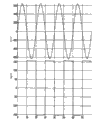
Figure 63 is the simulation waveform of Fig. 6 and the common high-frequency driving signal that produces of Fig. 8, be successively from top to bottom: the 555 Symmetrical square-wave voltage Gc that produce, the Symmetrical square-wave signal Va with respect to middle heart that produces on resistance R 12, the Symmetrical square-wave signal Vb with respect to middle heart that produces on resistance R 11, the Symmetrical square-wave signal Ga with respect to middle heart that produces on resistance R 14, the Symmetrical square-wave signal Gb with respect to middle heart that produces on resistance R 13.
Figure 64 is the simulation waveform of Fig. 7 and the common synchronized signal that produces of Fig. 8, and waveform title and meaning are the same.
Fig. 9 is active rectification circuit (3.1), field effect transistor Q17, the element circuit SBP that Q18 forms, it leaks level and is connected to transformer, basic circuit (2.2), input sine wave voltage V13 does not pass through rectifying and wave-filtering, when grid meets symmetrical square wave driving signal V9, the limit of paying at transformer TX2 produces the double-side band square-wave voltage Vs that envelope is sine wave, Vs can be divided into four different parts, be front 10 milliseconds upper, lower part and rear 10 milliseconds upper, lower part, V14-V17 is to be the civil power synchronizing signal of 20ms in the cycle, V15 wherein, the V16 10ms that delays time, V14, the V17 0ms that delays time, according to the direction of diode D11-D14 as can be known, D11, the upper part voltage of 10ms before the Q13 branch road is selected, so obtain only having the steamed bun wave voltage Va+ of positive half wave on source resistance R6, D13, the lower part voltage of 10ms after the Q15 branch road is selected, so obtain only having the steamed bun wave voltage Va-of negative half period on source resistance R7, D14, the lower part voltage of 10ms before the Q16 branch road is selected, so obtain only having the steamed bun wave voltage Vb-of negative half period on source resistance R9, D12, the upper part voltage of 10ms after the Q14 branch road is selected, so obtain only having the steamed bun wave voltage Vb+ of positive half cycle on source resistance R8, when output voltage from Q13, the source electrode of Q15 is obtained, output voltage is the whole steamed bun wave voltage Va2x of all-wave, when output voltage from Q15, the source electrode of Q17 is obtained, output voltage is the steamed bun wave voltage Vb2x of full-wave rectification, the waveform of Va2x and Vb2a is identical.
Figure 65 is the simulation waveform of output voltage, is successively from top to bottom: input current voltage Vi, transformation is paid polygonal voltage Vs, and rectification steamed bun wave voltage Va+, Va-, Va2x, Vb+, Vb-, Vb2x.Can see from the simulation waveform of Figure 65, although TX2 pays polygonal voltage waveform Vs about X-axis and asymmetric, but after over commutation and little capacitor C 6, C7, C8, C9 filtering, voltage waveform Va+ and Va-, Vb+ and Vb-are symmetrical about X-axis, the amplitude of Va2x and the every 10ms of Vb2x also equates, the aforementioned judgement of paying limit double-side band voltage about transformer of sufficient proof: look that the positive-negative half-cycle amplitude differs larger, but the pulse that amplitude is large is narrow, the pulse that amplitude is little is wide, and its area or mean value equate.
Figure 10 is active rectification circuit (3.2), the element circuit SBP that field effect transistor Q9, Q10 form, it leaks level and is connected to transformer, basic circuit (2.2), input sine wave voltage V3 does not pass through rectifying and wave-filtering, under the driving of high-frequency square-wave signal V9, transformer TX1 pays the limit and produces the double-side band square-wave voltage Vs that envelope is sine wave, identical with above-mentioned situation, but because the source electrode of Q5, Q7 is linked together, the source electrode of Q6, Q8 is linked together, obtains respectively positive and negative sine voltage Vsinx and V (sinx) on common source resistance R 2, R3.
Figure 66 is the output voltage simulation waveform of active rectification circuit (3.2), be successively from top to bottom: input voltage Vi, paying the limit envelope is sinusoidal wave double-side band voltage Vs, (sinx), the voltage Vsinx of output on resistance R 2 of the output voltage V on resistance R 3.
Figure 11 (A) is active rectification circuit (3.3), the element circuit (1.2) that field effect transistor Q19, Q20 form, it leaks level and meets transformer TX2, basic circuit (2.2), input sine wave voltage Vi does not pass through rectifying and wave-filtering, grid adds Symmetrical square wave driving signal V11, produces on the limit of paying of TX2 the double-side band square-wave voltage Vs that envelope is sine wave.
Q5 in Figure 11 (A), Q11 and Q6, Q12 forms respectively two element circuits (1.2), drive signal V5, V9 is synchronous square wave driving signal, cycle 10ms, Symmetrical, both single spin-echos, positive direction drives Q5, Q6, negative direction drives Q11, Q12, according to the principle of element circuit (1.2) as can be known, what first element circuit (1.2) obtained is the voltage on front 10ms top, just lower negative on voltage on capacitor C 2, waveform with Vs before the envelope of 10ms upper part waveform, what second element circuit (1.2) obtained is the voltage of part under rear 10ms, under negative on voltage on capacitor C 3 just, waveform with Vs after the envelope of part waveform under 10ms, from Q11, the voltage of Q12 source electrode output V2sinx, amplitude is 2 times of Vs, with the same homophase frequently of input voltage V4.Can see, under the front 10ms of Vs, not taking-up of 10ms upper part voltage after part voltage and Vs, be equivalent to halfwave rectifier voltage.
Figure 11 (B) is active rectification circuit (3.4), Q3, Q9, Q4, Q10, Q15, Q21, Q16, Q22 forms respectively four element circuits (1.2), drive signal V6, V7, V12, V13 is the Symmetrical square wave of cycle 20ms, anti-phase, according to the principle of element circuit (1.2) as can be known, when front 10ms drives the negative half period arrival of signal, Q9, Q10, Q21, the Q22 conducting, Q3, Q4, Q15, in the Q16 body, diode has formed a positive rectifier bridge, the result of rectification, make the waveform of front 10ms double-side band square-wave voltage Vs below time shaft, translating into the top of time shaft comes, the positive steamed bun wave voltage of 10ms before obtaining on load resistance R3, when rear 10ms drives the positive half cycle arrival of signal, Q3, Q4, Q15, Q16 conducting, in Q9, Q10, Q21, Q22 body, diode has formed a negative rectifier bridge, the result of rectification, make the waveform of double-side band square-wave voltage Vs above time shaft of rear 10ms, translate into the below of time shaft and come, the negative steamed bun wave voltage of 10ms after obtaining on load resistance R3.On resistance R 3, positive and negative two steamed bun wave voltages have formed the voltage waveform of a sinusoidal wave complete cycle, its amplitude is identical with the amplitude that transformer is paid polygonal voltage Vs,, homophase same frequently with input voltage, 10ms before and after Vs, the waveform of time shaft up and down all arrives load, is equivalent to full-wave rectifying circuit.
Figure 67 is the simulation waveform of C type and D type active rectification circuit output voltage, be successively from top to bottom: input voltage V4, transformer pay polygonal voltage Vs, the dynamic whole circuit output voltage V2sinx of C type, the dynamic whole circuit output voltage Vsinx of D type, the amplitude that can see V2sinx is 2 times of Vsinx.
Figure 12 is the schematic circuit of panel height modulation circuit (4), Q3, Q6 component units circuit (1.1), source electrode is connected to resistance R 6, typical basic circuit (2.1), voltage on load resistance is with combining grid voltage Vf, Vf is provided by the reference voltage Vc that produces in machine, and Vc controls malfunctioning a little more than civil power Vi to prevent grid.When: 1) load R5 changes, 2) city's electro-mechanical wave, 3) temperature changes, fluctuation can appear in grid voltage Vf, and output voltage V o also can fluctuate thereupon, in order to compensate this fluctuation, keep output voltage V o constant, must adjust grid voltage Vf in good time, keep grid voltage constant, to compensate above-mentioned three kinds of fluctuations that reason causes.
Keep direct voltage constant, a lot of alternative circuit are arranged, but the grid reference voltage Vf of this place is sine wave AC voltage, the opinion with available circuit can be stablized alternating voltage without any a kind of circuit; Really, the pulse-width modulation PWM technology, can stable DC and alternating voltage, but its operation principle is the pulsewidth of regulating high-frequency impulse is (the addressing before its drawback) on basis, main power component of the present invention does not carry out the conventional power conversion, and is adjustable without pulsewidth, therefore, keep grid voltage Vf constant, only have timely adjustment gate bias resistor R1 or R5.
Panel height modulation circuit (4) technology just automatically, the resistance of timely adjustment biasing resistor R1 or R5, the amplitude of indirect regulation sine wave AC reference voltage Vf makes its maintenance constant, its operation principle is as follows:
When input voltage Vi rises or descends, or load resistance R6 increases or when reducing, the amplitude of source electrode output voltage V o rises or descends, in the time of still between DC reference voltage V1 and V2, and as shown in the middle waveform of Figure 68, panel height modulation circuit attonity;
When input voltage Vi rises, when perhaps load resistance R6 increases, the amplitude of source electrode output voltage V o rises to greater than DC reference voltage V1, as shown in the superiors' waveform of Figure 68, in order to make Vo keep stable, the grid potential of Q3, Q6 is descended, the upper resistance R 1 of biasing is increased, R1 constantly increases, and Vo will constantly descend, after the amplitude of Vo drops to less than DC reference voltage V1, R1 just no longer increases, Vo also just no longer descends, and as the middle waveform of Figure 68, keeps the amplitude of output voltage V o less than V1;
When input voltage Vi descends, when perhaps load resistance R6 reduces, the amplitude of source electrode output voltage V o drops to less than DC reference voltage V2, orlop waveform as Figure 68, in order to make Vo keep stable, must make the grid potential of Q3, Q6 increase, upper offset resistance R 1 is reduced, R1 constantly reduces, and Vo will constantly rise, after the amplitude of Vo rises to greater than DC reference voltage V2, middle waveform as Figure 68, R1 just no longer reduces, and Vo also just no longer rises, and keeps the amplitude of output voltage V o greater than V2.
The result of above-mentioned dynamic adjustment, just the amplitude of output voltage V o only changes between DC reference voltage V1, V2, and V1, V2 can artificially set in advance, that is the amplitude of output voltage V o and the precision of voltage regulation can artificially be set in advance.Here the variation of R1 is not continuous, but quantification or digitized, its method is that the adjustable part of resistance R 1 is divided into the N equal portions, and each equal portions resistance is in parallel with a digital switch, and switch disconnects, represent this equal portions resistance access or increase, switch is closed, represents this equal portions resistive short or minimizing, the disconnection of switch and closure, automatically controlled by digital circuit, speed is exceedingly fast.
Panel height modulation circuit technology little change increment of Digital Circuit Control resistance R 1 adjustable part, to have controlled power device Q3, the sinusoidal wave dynamically amplitude of reference voltage Vf of Q6 grid in essence, therefore claim the panel height modulation, the ingenious part of this law is, reference voltage is DC low-voltage, and the object of control is but ac high voltage.In actual applications, N can get 8 or 16, and the circuit of realization is fairly simple, if the N value is excessive, and the circuit more complicated that can become.Panel height modulation circuit AHM and pulse-width modulation PWM have play the same tune on different musical instruments wonderful, can integrated various chip, and N can get larger value, and the adjusting of voltage is more accurate, more level and smooth, should use more convenient.
panel height modulation circuit AHM technology is according to the amplitude of alternating voltage Vo, automatically, the resistance of timely adjustment biasing resistor R1 or R2, its external circuit is very simple, one is control object: ac output voltage Vo, one is destination object: resistance R 1 or R2, in side circuit, can be with the resistance of a mark control object Vo, come whole circuit of equivalent panel height modulation circuit, the mask method of equivalent resistance is as follows: AHMn (Vo) No, AHM represents the panel height modulation circuit, n represents the adjustable Standard resistance range of destination object, (Vo) expression control object, No represents the sequence number of element.
Figure 13 is the side circuit of panel height modulation circuit, the course of work is as follows: U3, U4 form synchronous generator, produce the clock signal C lk of synchronizeing with civil power, it is voltage high detection circuit that U12, U13 form, when output voltage set during greater than V1, U19, U20 form the low testing circuit of voltage, reset during less than V2 when output voltage, U27, U28 form start reseting signal generating circuit, output Clr and RST signal.
R6, R7, R13, R14, R18, R19, R24, R25, R29, R30, R36, R37, R41, R42, R51, 16 switch in parallel such as 16 resistance such as R52 and S1-S16, U1, U7, U10, U14, U17, U21, U23, U25, U2, U8, U11, U15, U18, U22, U24, disconnection and the closure of 26 D flip-flop such as 16 of grades (74LS74) control switch S1-S16, namely control disconnection and the access of 16 resistance such as R1, U6 is four BCD forward-backward counters, initialize data end position D0-D2 connects high level by resistance R 47, D3 ground connection, initialize data is 0111, four terminal count output Q0-Q3 meet the data input pin A0-A3 of U16 four bit decoders, U16 is translated into 16 control signal Q0-Q15 to four binary-coded decimals that U6 counts to get, one of corresponding 16 D flip-flops such as U1 of each control signal, each D flip-flop is controlled disconnection and the access with 16 resistance such as R6, the adjustable part of the resistance R 1 that these 16 resistance are exactly Figure 12, the resistance R 58 of connecting with 16 resistance such as R6 is the resistance R 2 of Figure 16, V5 is the control voltage Vc in Figure 12, direct current reference circuit V1, V2 is respectively 3.0V and 2.9V.
U3 is comparator LM339, anti-phase termination is slightly larger than zero low level V0, steamed bun wave voltage Vd after homophase termination output voltage V o rectification, when this voltage during greater than V0, U3 exports high level, when this voltage during lower than V0, and the U3 output low level, obtain the square-wave voltage of synchronizeing with civil power at the output of U3, this voltage is received the input B of U4; U4 is monostable trigger, and its input B is that high level triggers, and C1, R1 have determined that the pulse of its output is 5ms, and obtaining the cycle at the output QP of U4 is 10ms, and pulsewidth is 5ms clock signal C lk, please refer to the simulation waveform of Clk in Figure 101 3.
U12 is comparator LM339, anti-phase termination reference voltage V1=3V, steamed bun wave voltage Vd after homophase termination output voltage V o rectification, when the steamed bun wave voltage after output voltage V o rectification during greater than V1, U12 exports high level, when this voltage during lower than V1, and the U12 output low level, obtain the square-wave voltage of synchronizeing with the civil power half period at the output of U12, this voltage is received the input B of U13; U13 is monostable trigger, its input B is that high level triggers, C2, R17 have determined that the pulse cycle of its output is slightly larger than 5ms, and the output QP at U13 obtains DC level rather than square-wave voltage, but that is monostable trigger U13 become a repeated trigger monostable trigger.
U19 is comparator LM339, anti-phase termination reference voltage V2=2.9V, steamed bun wave voltage Vd after homophase termination output voltage V o rectification, when this voltage during greater than V2, U19 exports high level, when this voltage during lower than V2, and the U19 output low level, obtain the square-wave voltage of synchronizeing with the civil power half period at the output of U19, this voltage is received the input B of U20; U20 is monostable trigger, its input B is that high level triggers, C3, R31 have determined that the pulse cycle of its output is slightly larger than 5ms, and the output QP at U20 obtains DC level rather than square-wave voltage, but that is monostable trigger U19 become a repeated trigger monostable trigger.
U27 is comparator LM339, half of anti-phase termination V3 voltage, voltage that in-phase end connects is slightly larger than end of oppisite phase voltage, is connected to simultaneously capacitor C 5, when start powers up, because capacitor C 5 both end voltage can not be suddenlyd change, in-phase end institute making alive is 0V, the U27 output low level, when the C5 both end voltage rises to greater than end of oppisite phase voltage, U27 exports high level, and at the output of U27 obtain starting shooting power-on reset and clear signal Clr, this voltage is received the input B of U28; U28 is monostable trigger, and its input B is that high level triggers, and C5, R46 have determined that the pulse cycle of its output is 1ms, at the output QP of U28 obtain starting shooting power-on reset and clear signal Clr, please refer to the simulation waveform of Clr in Figure 23.
The count results Q0-Q3 of four binary-coded decimal forward-backward counter U6 (74LS193) directly enters the A0-A3 of 4-16 decoder (74LS156) U16, each 4 binary-coded decimal determining is by after decoder, corresponding with one that determines in output Q0-Q15, the input end of clock of 16 D flip-flops such as U1 is received in the output of decoder, with 4 those D flip-flop actions that binary-coded decimal is corresponding.
During start, the negative pulse of the QN of U28 output 1ms resets U6, after reset pulse, QP chooses U16, and 16 D flip-flops such as U1 are resetted, 16 switches such as S1 disconnect, 16 resistance access circuits such as R6, and the amplitude of reference voltage Vf is minimum.The bridge that output AC voltage Vo is comprised of D1-D4 is rectified into the steamed bun wave voltage, and this voltage and direct voltage V1, V2 compare, and has three kinds of situations to occur:
1, when this voltage magnitude during less than direct voltage V1, greater than direct voltage V2, the QP of U13 and the QN of U20 be output low level, clock signal C lk can not by with door U5, U9, the Up of U6, Down pulse-free signal, the U6 counting stops.No matter data terminal, which kind of level of clock termination of 16 D flip-flops of U1 beginning, switch S 1-S16 is failure to actuate, and reference voltage Vf is constant, and within the amplitude of output voltage V o remained on allowed band, simulation waveform please refer to Figure 69.
2, when this voltage magnitude during greater than direct voltage V1, also greater than direct voltage V2, the QP output high level of U13, the QN output low level of U20, clock signal can not can be passed through U9 by U5, enter the input Down of U6, so U6 begins to subtract a counting, until the amplitude of output voltage V o is during less than V1, U6 stops counting.Because the QP of U20 exports high level, Q1 is anti-phase by triode, so what the data terminal D of 16 D flip-flops of U1 beginning connect is low level, if the clock end of certain D flip-flop has pulse to arrive, its output Q is low level, and this low level makes the switch that is attached thereto disconnect, with the resistance access circuit of switch in parallel, reference voltage Vf reduces, and output voltage V o also descends thereupon.As long as the amplitude of the steamed bun wave voltage Vd of output voltage V o is greater than direct voltage V1 (3.0V), U6 just constantly subtracts 1 counting, count results is through LS154 decoding, always with one D flip-flop is corresponding at last, make and want that with it the switch that contacts disconnects, corresponding resistance access circuit, consequently reference voltage Vf constantly descends, output voltage V o also constantly descends thereupon, and simulation waveform please refer to Figure 70.
3, when this voltage magnitude during less than direct voltage V1, also less than direct voltage V2, the QP output low level of U13, the QN output high level of U20, clock signal can not can be passed through U5 by U9, enter the input Up of U6, so U6 begins to increase a counting, until the amplitude of output voltage V o is during greater than V2, U6 stops counting.Because the QP output low level of U20, Q1 is anti-phase by triode, so what the data terminal D of 16 D flip-flops of U1 beginning connect is high level, if the clock end of certain D flip-flop has pulse to arrive, its output Q is high level, and this high level makes the switch that is attached thereto closed, with the resistive short of switch in parallel, reference voltage Vf raises, and output voltage V o also rises thereupon.As long as the amplitude of the steamed bun wave voltage Vd of output voltage V o is less than direct voltage V2, U6 just constantly adds 1 counting, count results is through LS154 decoding, always with one D flip-flop is corresponding at last, make switch associated therewith closed, resistive short, consequently reference voltage Vf constantly rises, output voltage V o also constantly rises thereupon, and simulation waveform please refer to Figure 71.
Boost capacitor network UPnet is comprised of N rank capacitance network, in Figure 14, is the firstorder circuit figure of network from Begin to End, and there are left and right two arms, circuit full symmetric in every rank; Decompression capacitor network DNnet is comprised of N rank capacitance network, in Figure 15, is the firstorder circuit figure of network from Begin to End, and there are left and right two arms, circuit full symmetric in every rank.
Embodiment
Embodiment 1: ac inverter.
Figure 16 is ac inverter, metal-oxide-semiconductor Q25, Q27 etc. form A type element circuit SBPA, meet transformer TX2 in its common drain electrode, consist of basic circuit (2.2), transformer is paid the active rectification circuit (3.4) that the limit is Q17, Q18, Q19, Q20, Q23, Q24, Q28, Q29 composition, and C2 has been the electric capacity of smoothing effect, and V17 is civil power, V18, V19, V25, V26 are the VDvrs type synchronized signals of Symmetrical, and V22, V24 are VDvrh type high-frequency driving signals.If the amplitude of input voltage V17 is 280V, the no-load voltage ratio of transformer TX1 is 1:0.3, and load resistance R7 is 50 Europe, and on resistance R 7, output amplitude is the alternating voltage Vo of 80V.In the simulation waveform of Figure 72, that input voltage Vi, transformer are paid double-side band square-wave voltage Vs, the output voltage V o of limit envelope for sine wave successively, can see, output voltage and input voltage are with frequency, homophase, it is the envelope that transformer is paid limit double-side band voltage waveform, change the pulsewidth that drives signal V22, V24, namely duty ratio, can adjust automatically to output AC voltage Vo.
Embodiment 2: dc inverter.
Figure 17 is dc inverter, and metal-oxide-semiconductor Q33, Q34, Q37, Q38 form main circuit, and because input voltage is direct current, the metal-oxide-semiconductor polarity of component units circuit is identical, exempts simultaneously the diode that joins with it.applied voltage V16 is the direct voltage of 311V, drives signal V24, V25 is the square-wave signal of 50Hz, and V25 hysteresis 10ms drives signal G1, G3 is by Q29, the envelope that Q30 produces is the high-frequency square-wave signal of sinusoidal steamed bun ripple, G3 hysteresis 10ms, and during front 10ms, Q33, the Q38 conducting, direct voltage is through TX3 former limit winding, Q33, R12, Q38 forms the loop, produces the sinusoidal forward steamed bun wave height identical with G1 envelope square-wave voltage frequently on R12, produces the sinusoidal steamed bun wave height of double-side band square-wave voltage frequently on the limit of paying of TX3, during rear 10ms, and Q34, the Q37 conducting, direct voltage is through TX3 former limit winding, Q34, R12, Q37 forms the loop, produce the sinusoidal negative direction steamed bun wave height identical with G3 envelope square-wave voltage frequently on R12, the limit of paying at TX3 produces the sinusoidal steamed bun wave height of rear 10ms double-side band square-wave voltage frequently, through 20ms, forming complete envelope on resistance R 12 is sinusoidal wave high frequency square wave voltage Voa, pay the limit at TX3 and form the sinusoidal wave high frequency square wave voltage Vs of complete double-side band, voltage Vs is through Q25, Q26, Q31, Q32, Q35, Q36, Q39, after the D type active rectification circuit that Q40 forms, produce sinewave output voltage Vob, the no-load voltage ratio of TX3 and G1, the amplitude of Vob can be controlled and regulate to the pulsewidth of G3.
The source electrode of the generation of G1, G3: Q27, Q28 is connecting resistance R10, R11 respectively, the grid source electrode connects high frequency square wave and drives signal V17, V18, drain electrode meets respectively square-wave signal V19, the V20 of cycle 20ms, duty ratio 50%, V20 hysteresis 10ms, so obtaining the envelope cycle on resistance R 10, R11 is that 20ms, duty ratio are 50% high-frequency square-wave signal Vr3, Vr4, wherein Vr4 is than the Vr3 10ms that lags behind.After the full-bridge of the sine wave signal of 50Hz, the amplitude 322V that produces in machine through the D1-D4 composition, produce steamed bun ripple signal, be added in the drain electrode of Q29, Q30, their source electrode is respectively by resistance R 13, R14 ground connection, the grid source electrode meets respectively driving signal Vr3, the Vr4 on R10, R11, respectively obtains amplitude 320V, envelope and be sinusoidal wave half steamed bun ripple signal G1, G3 on source resistance R13, R14.
Figure 73 is the simulation waveform of each point voltage, is successively from top to bottom: drive signal Vr3, Vr4, drive signal G1, G3, TX3 pays limit double-side band voltage Vs, the sine voltage Voa of R12 output, the sine voltage Vob that active rectification DR produces.
If the sine wave that cuts down is ASinx, after the cutting, the expression formula of residue part is S=A-ASinx, and S is the result of translation after SIN function ASinx counter-rotating, is still SIN function, so pay at transformer TX3 the double-side band square-wave voltage that the limit obtains, its envelope is still sinusoidal wave.
Q33, Q34 consist of main clipper circuit, the commutation of Q37, Q38 guide current, and when its effect is equivalent to exchange input, the diode that joins with metal-oxide-semiconductor.Output voltage V oa on R12 is immediately following grid voltage G1, G3, and its amplitude hang down a Vgs, and after passing through capacitor C 10 filtering, its waveform is no longer square-wave voltage, but with signal G1, sine voltage that the G3 envelope is identical.
The clipper circuit that Q33, Q34 form downcuts sine voltage Voa to the direct voltage that is added in drain electrode, area is 64% of input voltage, residue after cutting partly accounts for 36% of input voltage area, and this part voltage through the conventional power conversion, produces sine voltage Vob in TX3.Voa is the source voltage that cuts down, its conversion efficiency is 100%, Vob carries out output voltage after the conventional power conversion by TX3, its conversion efficiency is 85%, if the power loss of this part is P1, P1=36%* (1-85%)=5.4%, useful work is that gross efficiency is 94.56%.
Embodiment 3: alternating current steady voltage plug.
Figure 18 is the schematic circuit of alternating current steady voltage plug, power device Q1, Q3 form A type element circuit SBPA, be connected to resistance R 7 at common source, consist of basic circuit (2.1), panel height modulation equivalent resistance AHM20k (Vo) 1 and resistance R 6 are biasing circuits of Q1, Q3 grid, and input voltage Vi is that amplitude is the sine wave of 360V.Output voltage V o follows the tracks of the grid voltage of Q1, Q3, when upper offset resistance at 10k when changing between 100k, output voltage V o changes between 170V at 300V, namely ac output voltage is adjustable, Figure 74 is the simulation waveform of output voltage; When load resistance R7, input voltage Vi or temperature T changed, respective change can occur in output voltage V o, and panel height modulation circuit this moment (4) starts, and the result of closed-loop control makes output voltage keep constant.The mark meaning of panel height modulation equivalent resistance AHM20k (Vo) 1 is: the adjustable Standard resistance range of upper offset resistance AHM1 is 20k, and control object is output voltage V o.
If input voltage 250V, source electrode output voltage 220V, output current 20A has the AC voltage drop of 30V at the drain-source utmost point of Q1, Q3, and power loss is 600W, and overall efficiency is 88%.In order to make Q1, the unlikely heating waste of Q3 drain-source 30V alternating voltage, the drain electrode of the element circuit that Q1, Q3 form meets transformer TX1, this partial power (12%) is carried out the conventional power conversion, with output voltage V o parallel output, as shown in figure 19.
In Figure 19, the common drain electrode of the element circuit (1.1) that Q13, Q14 form meets transformer TX1, be evolved into basic circuit (2.3), grid at two power device Q13, Q14 adds VDvrh type high-frequency driving signal V8, V10, applied voltage V1 is 250V, source electrode output voltage V oa is 220V, and transformer primary side winding and Q13, Q14 drain-source pressure drop sum are 30V.Because Q13, Q14 are operated near the saturation region, its drain-source pressure drop is very little, 30V voltage all is added in the former limit of transformer basically, the no-load voltage ratio of TX1 is 11, the limit generation amplitude of paying at TX1 is the double-side band square-wave voltage of sine wave near 311V, envelope, after this voltage process active rectification circuit (3.4), obtain sine voltage Vob.Figure 75 is the simulation waveform of output voltage, be successively from top to bottom: input voltage Vi, transformer are paid limit double-side band square-wave voltage Vs, source electrode output voltage V oa, transformer is paid limit output voltage V ob, can see from simulation waveform, output voltage V oa, Vob and input voltage Vi are with the frequency homophase.
Due to output voltage and input voltage series connection, input current is identical with output current, during computational efficiency, the power voltage available replaces, input voltage 250V, wherein 220V is exported by source electrode, and surplus 30V is through the conventional power conversion, its conversion efficiency is 85%, this part output voltage is 30*85%=25.5V, so the actual 220+25.5=245.5V that is output as, and efficient equals power output divided by input power, therefore, the overall efficiency of Figure 19 AC voltage regulator is 245.5/250=98.2%.The exhausted major part (88%) of input power is exported by source electrode, through output needn't pass through core transformers, and the conversion efficiency of this partial power is 100%, only have very small portion power (12%) will carry out the conventional power conversion, and by the core transformers transmitted power.In the circuit of Figure 19, the basic circuit (2.3) that Q13, Q14 form cuts into two parts to input sine wave voltage Vi as a cutter, some is output AC voltage Voa, another is partly transformer primary polygonal voltage Vp, and therefore, the circuit of Figure 19 is the voltage cutting circuit.
Should guarantee that output voltage V oa is constant sine voltage, guarantee again the operating frequency of transformer TX1, the gate drive signal that is added in Q1, Q2 must be that envelope is sinusoidal wave square-wave voltage, and its amplitude should be slightly high with output voltage, and its frequency should be suitable with the operating frequency of transformer; In addition, during lower than 220V, must carry out voltage compensation, to reach the rated output voltage value when input voltage.
Figure 20 is the main circuit of AC voltage regulator, by the basic circuit (2.2) that Q57, Q58 form, adds pair limit circuit of transformer, is an ac inverter, and is identical with the circuit of Figure 16.The output voltage of inverter is connected with input voltage Vi, the alternating voltage Vr16 that is output on resistance R 16 connects with input ac voltage Vi, the live wire of the lower termination input voltage Vi of R16, another termination exit point Vc of R2, change the pulsewidth that drives signal V38, be duty ratio, can automatically adjust output voltage V c.
The basic circuit (2.1) that is formed by Q49, Q50, add the VDvrh type at its grid and drive signal, when adding AC power V35, the output envelope is sinusoidal wave square-wave signal on source resistance R18, the amplitude of its envelope is than the low Vgs of grid voltage, and its frequency is identical with the frequency that grid adds VDvrh type driving signal.The basic circuit (2.3) that is formed by Q51, Q54 and transformer thereof pay the limit circuit, form an AC voltage regulator, identical with the circuit of Figure 19, when square-wave signal that export when resistance R 18, that envelope is sine wave is added to the grid of Q51, Q54, the output voltage V oa that can guarantee its source electrode is the sine voltage of specified amplitude, also can guarantee the operating frequency of transformer TX4, transformer TX4 pays the output voltage V ob on limit in end points Va and source electrode output voltage V oa output in parallel.Panel height modulation equivalent resistance AHM30k (Voa) 1 connect with resistance R 18, and when AHM30k (Voa) 1 became large, the envelope of the upper output of R18 was that the square-wave signal amplitude of sine wave diminishes, and vice versa, indirectly control the amplitude of output voltage V oa.
The alternating current steady voltage plug course of work of Figure 20 is as follows: during in normal range (NR), compensating circuit and clipper circuit do not start as input voltage Vi, and output voltage is exactly input voltage Vi; When input voltage was too high, clipper circuit started, and compensating circuit does not start, and output voltage is Va; When input voltage was too low, clipper circuit did not start, and compensating circuit starts, and output voltage is Vc; The access of voltage Vi, Va, Vc and disconnection have special switch to control (please refer to uninterrupted power supply UPS).
Embodiment 4: D.C. regulated power supply.
Figure 21 is the schematic circuit of D.C. regulated power supply, the rectifier bridge that input voltage V2 forms through D3, D4, D13, D14, produce steamed bun wave voltage Vd, this voltage is added in the drain electrode of metal-oxide-semiconductor Q2 by resistance R 1, the source electrode of Q2 is by resistance R 9 ground connection, and its grid meets square wave driving signal V3, it is the square-wave signal Vc of steamed bun ripple that source electrode produces envelope, Vc becomes flat-top steamed bun ripple cutoff signal by the voltage-stabiliser tube heap slicing that D11, D12, D15 form, and is added in the grid of metal-oxide-semiconductor Q4.The circuit that Q4 and transformer TX1, resistance R 8 form is basic circuit (2.3), be half of clipper circuit, obtain the flat-top steamed bun wave voltage identical with cutoff signal on the source resistance R8 of Q4, the double-side band square-wave voltage of paying limit circuit generation of TX1 is by after full-bridge rectification, obtain direct voltage Vob, the amplitude of Voa, Vob is identical, two-way direct voltage parallel output.
Panel height modulation equivalent resistance AHM50k (Voa) 1, adjustable resistance is 50k, and controlled plant is output AC voltage Voa, and the adjustment of output voltage V ob has two approach, and the no-load voltage ratio of the one, TX1 is coarse adjustment, the 2nd, the pulsewidth of cutting square wave is fine tuning.
Figure 78 is the simulation waveform of each point voltage, be successively from top to bottom: steamed bun wave voltage Vd, killer voltage Vc, Q2 source electrode output voltage V oa, the TX1 of input voltage after rectification pays the output voltage V ob that limit double-side band voltage Vs, bridge rectifier obtain, here Voa, Vob do not strengthen capacitor filtering, are unidirectional pulsating voltages.
Adopting the benefit of flat-topped wave cutting is further to improve overall efficiency, Figure 76 is the comparison demonstration graph of cutting mode, export the 250V direct voltage, can be the sine wave signal cutting input voltage of 250V with amplitude, but the part of the residue after cutting, obviously greater than the residue part with 250V direct current signal cutting input voltage, the residue part of cutting is fewer, the power that need to carry out the conventional power conversion is fewer, efficient is also just higher, and the complete cutoff signal that this D.C. regulated power supply adopts is as shown in Figure 77.If input ac voltage is 220V, output dc voltage 250V, the input voltage area is P1=220*1.414*2=622 (V), and the head area of slicing is P2=51.45, and overall efficiency can be calculated as follows:
On resistance R 8, the flat-top steamed bun wave voltage area of output is P1-P2=(622-51.45)=570.55, the conversion efficiency of this part is 100%, head area 51.45 need to carry out the conventional power conversion, efficient is 85%, the available power of this part is 51.45*85%=43.73, overall efficiency is: (570.55+43.75)/622=98.75%, when output voltage was higher, overall efficiency was also higher.
Embodiment 5: ac uninterrupted power supply UPS.
On the circuit of alternating current steady voltage plug, additional direct voltage place in circuit and output voltage controlling circuit just become uninterrupted power supply UPS, physical circuit such as Figure 22.
Power device Q4, Q10, Q5, Q11, Q6, Q12 form three basic circuit (2.1), switch as alternating voltage, the three is referred to as output voltage controlling circuit, and this circuit is the some (please refer to alternating current steady voltage plug) of alternating current steady voltage plug.During in normal range (NR), the element circuit that joins with port Vi starts when input voltage, and input voltage forms pressure drop on source resistance R2, become output voltage V o; When input voltage was too high, the element circuit that joins with port Va started, and the voltage Va that clipper circuit produces forms pressure drop on resistance R 2, become output voltage V o; When input voltage was too low, the element circuit that joins with port Vc started, and the voltage Vc that compensating circuit produces forms pressure drop on resistance R 2, become output voltage V o.
The basic circuit (2.1) that power device Q9, Q3 form is charge-discharge circuit, the basic circuit (2.1) that power device Q2, Q8 form is the polarity of voltage change-over circuit, the basic circuit (2.1) that power device Q1, Q7 form is square wave conversion circuit, and the three is referred to as the direct voltage place in circuit.During lower than rated value, Q3 starts when battery tension, and to storage battery V13 charging, during higher than rated value, Q3 disconnects input ac voltage Vi, stops charging when battery tension through D3, Q3.
During mains failure, input voltage Vi is zero, and Q9 starts, the positive square-wave voltage that battery tension is exported cycle 20ms, pulsewidth 10ms, synchronizeed with civil power by Q9, D9; During front 10ms, this voltage divides two-way, leads up to D1, Q1, forms the positive half cycle of square-wave voltage Vp on resistance R, another road voltage by D2, Q2 and D14 to capacitor C 1 charging, just lower negative capacitance voltage Vc5 in formation; During rear 10ms, the storage battery no-output, the positive pole of voltage Vc5 on capacitor C 5 is by Q8, D8 ground connection, and its negative pole forms the negative half period of square-wave voltage Vp by D7, Q7 on resistance R 1, and the 50Hz square-wave voltage Vp that forms on resistance R 1 directly enters the input voltage bus.
After square-wave voltage Vp enters the input voltage bus, according to higher than, lower than two kinds of situations of rated voltage, just the same during with alternating voltage, carry out identical processing and control, cut during namely greater than rated value, compensate during less than rated value, the result of cutting and compensation, output voltage V o is sine voltage (please refer to dc inverter).
Embodiment 6: DC UPS UPS without the converter uninterrupted power supply.
Whole meanings of this title of uninterrupted power supply UPS mean that not only output voltage is uninterrupted, also mean simultaneously the purpose of output voltage, are mainly to provide electric energy to computer and peripheral hardware thereof.Because computer and peripheral hardware thereof all adopt Switching Power Supply, AC power enters the first step after computer, carry out exactly rectification, alternating voltage is made into direct voltage, input voltage is alternating voltage or direct voltage, get on very well for computer and peripheral hardware thereof, unimportant, so direct voltage can directly enter computer and peripheral hardware thereof.Whole meanings of DC UPS UPS possess same connotation: meaning not only that namely output voltage is uninterrupted, also mean simultaneously the purpose of output voltage, is mainly to provide electric energy to computer and peripheral hardware thereof.
Figure 23 is the main circuit diagram without the converter uninterrupted power supply, and the source electrode of the A type element circuit that is comprised of metal-oxide-semiconductor Q1, Q2 meets storage battery V2, and when civil power was arranged, civil power V1 directly powered to the load, and metal-oxide-semiconductor Q2 grid-control voltage Gp is low, the Q2 cut-off.During lower than rated value, Q1 grid control signal Gn is high when battery tension, the Q1 conducting, and to storage battery V2 charging, during greater than rated value, Q1 grid control signal Gn is low to civil power when battery tension through diode D1, metal-oxide-semiconductor Q1.Q1 turn-offs, and charging stops; When mains failure, metal-oxide-semiconductor Q2 grid control signal Gp is high, the Q2 conducting, and battery tension powers to the load by Q2, D2.Present embodiment is without any power inverter, therefore claim without the converter uninterrupted power supply.
When civil power is arranged, directly export civil power without the converter uninterrupted power supply, when mains failure, directly export accumulator DC and press, civil power and accumulator DC are pressed without any power conversion.Why can be like this, be based on following 2 reasons: one, computer and the occasion that is located at civil power outward thereof are moved very normally, why UPS will be installed, and are because civil power can unexpectedly interrupt rather than other reasons fully.Its two, computer and peripheral hardware thereof might not require Alternating Current Power Supply, the direct current supply meeting is better.
Embodiment 7: the UPS without power consumption of DC UPS UPS.
Figure 24 is the main circuit diagram of UPS without power consumption, with comparing without the converter uninterrupted power supply of Figure 23, has had more the full-bridge circuit that is comprised of diode D8, D9, D18, D19.The input voltage of UPS without power consumption UPS only passes through rectification circuit, and complete machine only is equivalent to the power consumption that a diode PN junction produces, and its micro power consumption is therefore claim UPS without power consumption.
UPS without power consumption is when having civil power, what export is the steamed bun pulsation wave voltage of civil power after rectification, when mains failure, what export is the direct voltage of the monolateral decline of storage battery, why can be like this, be based on following two reasons: one, computer and peripheral hardware thereof have all adopted switching power supply, input voltage is constant non-constant, concerning computer and peripheral hardware thereof, and indistinction.Its two, computer and peripheral hardware thereof might not require alternating voltage power supply, DC-voltage supply can be better.
Embodiment 8: the no-reverse change device uninterrupted power supply of DC UPS UPS.
Figure 25 is the main circuit diagram of no-reverse change device uninterrupted power supply, compare with the UPS without power consumption of Figure 24, had more the voltage compensating circuit that is formed by Q57, Q58, the direct voltage V55 that steamed bun wave voltage Vd behind the compensating direct current voltage that compensating circuit produces and input commercial power rectification or storage battery are exported connects, when inputting civil power lower than rated value, controllable silicon SCR 1 is turn-offed, bucking voltage and Vd or V55 are superimposed as output voltage V o, because bucking voltage is to carry out conventional power conversion (PWM) to come, adjusting pulsewidth can make output voltage V o keep constant; When civil power was not less than rated value, compensating circuit cut out, and SCR1 is open-minded, and all the other courses of work and UPS without power consumption are identical.
No-reverse change device uninterrupted power supply is when having civil power, that export is the constant voltage Vo of civil power after the steamed bun ripple Vd after rectification and bucking voltage Vc stack, when mains failure, what export is that accumulator DC is pressed the constant voltage Vo after V1 and bucking voltage Vc superpose, no-reverse change device uninterrupted power supply does not have inverter, direct current no longer is transformed into interchange, because computer and peripheral hardware thereof might not require the alternating voltage power supply, DC-voltage supply can be better.
Figure 26 is interchange detection and the storage battery testing circuit of no-reverse change device uninterrupted power supply, circuit divides two parts, front part is AC detection circuit, the steamed bun wave voltage Va of the homophase termination of comparator LM339 after with reference to ac voltage rectifier, the steamed bun wave voltage Vd behind anti-phase termination input commercial power rectification.Within rated range, voltage Vd is greater than voltage Va when the input civil power, and comparator LM339 output low level is turn-offed switch S 1; Less than rated range or when having a power failure, voltage Vd is less than voltage Va when the input civil power, and comparator LM339 export high level, makes switch S 1 open-minded, then signal voltage V30 be added between the grid source of Q56, the Q56 conducting, battery tension is exported provides load current.
rear part is the storage battery testing circuit, battery tension E01 receives the anode of optocoupler 4N33 diode part, form the loop by resistance R 14, triode partly is connected into emitter follower, through resistance R 12, R18 and R11, after the R19 dividing potential drop, the Trig of incoming clock chip 555/ALD and Thresh end, when storage battery is pressed in normal range (NR), the 555/ALD output low level, when battery tension during lower than rated value, 555/ALD exports high level, make switch S 2 open-minded, signal voltage V31 is added between the grid source of Q55, the Q55 conducting, steamed bun wave voltage after whole charges to storage battery.
This circuit has three interface signal: Gp, Gn, E01 with no-reverse change device uninterrupted power supply, UPS without power consumption and three same interface signals are also arranged without the converter uninterrupted power supply, the definition of signal is identical, and therefore, this testing circuit is fit to above-mentioned three kinds of DC UPSs.
Embodiment 9: exchange constant-current supply.
Figure 27 exchanges constant-current supply, the basic circuit (2.1) that is formed by Q47, Q48, meet output resistance R17 in its common drain electrode, difference parallel voltage-stabilizing diode D39, D38 on source resistance R10, R11, by the power MOS pipe characteristic as can be known, drain-source current is only relevant with grid voltage, when grid voltage is constant (by voltage stabilizing didoe D39, D38 voltage stabilizing), its drain-source current is also constant, when load changes, or input voltage is when changing, and output current is constant.Figure 79 is the simulation waveform of output current, and when load resistance R17 changed to 50 Europe from 10 Europe, it is constant that output current keeps; Figure 80 is the simulation waveform of output voltage, and when load resistance R17 changed to 50 Europe from 10 Europe, the upper output voltage of R17 changed to 280V from 60V, illustrated that also load current is constant.
Embodiment 10: direct current constant voltage supply.
Figure 28 is the direct current constant voltage supply, the input civil power is through D15, D16, D25, steamed bun wave voltage after the whole circuit of full-bridge that D26 forms, be added in the drain electrode of metal-oxide-semiconductor Q29, be added in simultaneously by resistance R 1 and voltage-stabiliser tube D21, D23, D24, on the voltage-stabiliser tube heap of D27 series connection, each voltage-stabiliser tube is 75V, the gate clamped of Q1 is at the 300V level, its source electrode is by resistance R 8 ground connection, produce the flat-top steamed bun wave voltage of 300V slicing on R8, this voltage is added in the source electrode of metal-oxide-semiconductor Q30 by resistance R 7, its drain electrode is by resistance R 9 ground connection, the grid source electrode meets voltage stabilizing didoe D17.According to the characteristic of metal-oxide-semiconductor, drain-source current is only relevant with grid voltage, and grid voltage is constant, and drain-source current is also constant, and now at certain level, so its drain-source current is constant, the output constant current electric current by voltage stabilizing didoe D3 clamper for the grid voltage of Q30; When the resistance of load resistance R5 increased to that on it, voltage surpasses permissible value, Q29 export constant voltage, has limited the R5 output voltage and has continued to increase, the maintenance pressure-keeping functions.
Figure 81 is the simulation waveform of output current, and load resistance R4 changes to 30 Europe from 8 Europe, and the electric current that flows through load resistance R18 is substantially constant; Figure 82 is the simulation waveform of output voltage, and load resistance R18 changes to 30 Europe from 8 Europe, and on it, voltage changes to 200V from 50V, illustrates that the electric current that wherein passes through keeps constant.
Embodiment 11: accessory power supply.
Figure 29 is accessory power supply, metal-oxide-semiconductor Q15 in circuit, Q17, Q16, Q18 forms two A type element circuit SBPA, their common source is connecting resistance R4 respectively, R5, consist of basic circuit (2.1), external power supply V20 is amplitude 311V civil power, drive signal V14, V18, V15, V19 is cycle 20ms, the square wave of pulsewidth 1ms, time-delay is successively: 0ms, 10ms, 9ms, 19ms, get respectively the voltage in 1ms interval, sinusoidal wave zero passage front and back, it is the simulation waveform of each point voltage as Figure 83, be successively from top to bottom: input ac voltage Vi, gate drive voltage V1, V2, V3, V4, output voltage V p on resistance R 4, output voltage V n on resistance R 5.V1-V4 is the interval selection pulse, can see, strobe pulse and output voltage tip interval are corresponding one by one.Figure 84 is the Symmetrical direct voltage after excessive capacitor filtering, and amplitude if select distinct pulse widths, can obtain the output dc voltage of different amplitudes near 80V.
Electric network pollution, power factor is low, main cause is that too many capacitive load is arranged, the characteristics of capacitive load are only to utilize near the interval little part voltage of sinusoidal wave peak value, if the interval that begins from zero passage utilizes sine voltage, not only develop a large treasure-house of the energy, and can greatly improve the pollution level of electrical network.
This accessory power supply has utilized near the interval sine voltage of zero passage just, suitably selects metal-oxide-semiconductor to drive the pulsewidth of signal, wants how low boost voltage, how lowly just can have.When selecting to drive signal pulsewidth 0.5ms, the output symmetrical voltage is the 30V left and right, and this voltage also can obtain direct-flow positive voltage after rectification.
Embodiment 12: polarity inversion power supply.
Figure 30 is the polarity inversion power supply, and function is the polarity negate voltage.The common source connecting resistance R5 of metal-oxide-semiconductor Q1, Q12 and the series arm of C7, D20, the minus earth of D20, input voltage V12 is positive voltage, driving signal V9, V10 is the square wave of 50Hz.During front 10ms, the Q11 conducting, V12 forms the square-wave voltage of 10ms on resistance R 5, charge to capacitor C 7 by D20 simultaneously, and is just lower negative on polarity; When second 10ms arrives, the Q11 cut-off, the Q12 conducting, the positive voltage terminal ground connection of C7, diode D17 is the output negative voltage, so obtain the losing side wave voltage of 10ms on resistance R 6.The simulation waveform of Figure 85 is positive negative pulse stuffing voltage, obtain the output of symmetrical direct current, can strengthen filter capacitor, and in fact, the circuit on Figure 49 left side is also a square wave inverting power source.The polarity inversion power supply is often used in follow-up embodiment.
Embodiment 13: AC to AC N rank booster power.
Figure 31 is AC to AC N rank booster powers, and the right and left circuit full symmetric is existing take N=4 as example.Metal-oxide-semiconductor Q11, Q4 form A type element circuit, and source electrode meets N rank boost capacitor network UPnet, the element circuit that Q1, Q8 form, and 1, two element circuit of its common source connecting resistance R1 and capacitor C all is connected into basic circuit (2.1).For boost capacitor network the first rank, between positive half period, Q11 is logical, V34 charges to capacitor C 2 by diode D7, D11, D17 and Q23, between negative half-cycle, the Q4 conducting, to capacitor C 3 chargings, other three rank charging modes of boost capacitor network are identical by diode D9, D12, D18 and Q38 for V34.Charging and discharging carries out simultaneously, between positive half period, Q4, Q15, Q21, Q27, Q8 conducting, form the negative sense pressure drop after voltage superposition on capacitor C 3, C10, C17, C23 on resistance R 1, between negative half-cycle, Q11, Q18, Q24, Q30, Q1 conducting form forward voltage drop after the voltage superposition on capacitor C 2, C9, C16, C22 on resistance R 1, charging and discharging hockets, and output voltage V o is than input voltage V11 hysteresis half period.Figure 86 is the simulation waveform of output voltage, and intermediate sinusoids is the 311V mains waveform, and skin is the square-wave output voltage that has boosted near 1200V.
The efficient of this power supply can be estimated as follows:
Load resistance R1 is 1k, output voltage 1200V, and output current 1.2A, the voltage on positive half cycle and negative half period network capacitance is superposition output, it is identical that charging current and discharging current can be thought.The diode forward saturation voltage drop is 1.2V, and metal-oxide-semiconductor saturation conduction resistance is 0.75 Europe, and each charge tunnel has three diodes, a metal-oxide-semiconductor, and its voltage loss is:
U1=1.2*3+0.75*1.2=4.5V
Because the circuit of capacitor charging is connected, electric current is identical, and the computational efficiency voltage available replaces, and the voltage loss of four charge tunnels simultaneously is identical, and the efficiency eta 1 when charging is:
η1=(311-4.5)/311=98.56%
Discharge channel has four metal-oxide-semiconductors, a diode, and voltage loss is:
U2=0.75*4*1.2+1.2=4.8V
As a same reason, discharging efficiency η 2 is:
η2=(1200-4.8)/1200=99.6%
So, gross efficiency η=η 1* η 2=98.56%*99.6%=98.17%
Embodiment 14: AC-to DC N rank booster power.
Figure 32 is AC-to DC N rank booster powers, and is existing take N=4 as example, present embodiment and upper example have following 2 different: 1) the direct ground connection of the source electrode of metal-oxide-semiconductor Q9; 2) series arm of adjunction C15 and D39 between the anode of diode D32 and ground, the plus earth of D39.
Present embodiment is to exchange input, but can export direct current, the place that its course of work is not identical with execution mode 10 is: 1) between negative half-cycle, not conducting of Q9, after voltage superposition on capacitor C 5, C12, C19, C25, by diode D39 to capacitor C 15 charging, the voltage direction on C15 be upper negative under just.2) at the positive half cycle of next cycle, the Q9 conducting, the negative voltage side of capacitor C 15 (upper end) ground connection, positive voltage terminal (lower end) output voltage V b, this voltage forms positive pressure drop by diode D33 on load resistance R2.Figure 87 is the output voltage simulation waveform, and the above is the input civil power Vi of 311V, and the centre is output voltage V a, amplitude is the positive square-wave voltage of 1200V, and the bottom is Vb, and amplitude is also the forward square-wave voltage of 1200V, Vb and Va export side by side, and phase place is identical, overlap.
Embodiment 15: direct current is to exchanging N rank booster power.
Figure 33 is that direct current arrives and exchanges N rank booster power, compares 1 with AC to AC 4 rank booster powers) replace 2 diodes in the charging end with 2 metal-oxide-semiconductors, because be the direct current input, control with full control device metal-oxide-semiconductor the opportunity of charging; 2) increased the polarity upset circuit that is formed by C26, D59, Q35, the negative-going pulse voltage of generation cycle 20ms, hysteresis 10ms, the drain electrode of Q6 is equivalent to add and exchanges negative half period voltage, and the course of work after this and AC to AC N rank booster power are identical.Figure 88 is the simulation waveform of output voltage, and 0.2 and 0.4 middle straight line is input 300V direct voltage V+, and 0 and-0.3 middle square-wave voltage is the pulse voltage V-of polarity upset circuit generation-300V, and outermost layer is the output voltage V o of 1200V symmetrical square wave.
Embodiment 16: the AC to AC N high-frequency and high-voltage power supply that boosts on rank.
Figure 34 is the AC to AC N rank high-frequency and high-voltage power supplies that boost, compare with AC to AC 4 rank booster powers, 2 differences are arranged: 1) replace 2 diodes in the charging end with 2 metal-oxide-semiconductors, because will control charge frequency, must control with full control device metal-oxide-semiconductor the opportunity of charging; 2) operating frequency is brought up to 1KHz from 50Hz, and this operating frequency is optional, and operating frequency is exactly the output voltage frequency of output high-frequency and high-voltage power supply.Figure 89 is the simulation waveform of output voltage, and intermediate sinusoids is that amplitude is the input voltage Vi of 250V, and the symmetrical square wave of 1000V is the high-frequency and high-voltage Vo of output.
Embodiment 17: the AC-to DC N high-frequency and high-voltage power supply that boosts on rank.
Figure 35 is the AC-to DC N rank high-frequency and high-voltage power supplies that boost, compare with AC-to DC 4 rank booster powers, 2 differences are arranged: 1) replace 2 diodes in the charging end with 2 metal-oxide-semiconductors, because will control charge frequency, must control with full control device metal-oxide-semiconductor the opportunity of charging; 2) operating frequency is brought up to 1KHz from 50Hz, and this operating frequency is optional, and operating frequency is exactly the output voltage frequency of output high-frequency and high-voltage power supply.Figure 90 is the simulation waveform of output voltage, and the right sine wave is that amplitude is the input voltage Vi of 250V, and the square wave of left side 1000V is the high-frequency direct-current high pressure Vo of output.
Embodiment 18: direct current is to exchanging the N rank high-frequency and high-voltage power supply that boosts.
Figure 36 is direct current to exchanging the N rank high-frequency and high-voltage power supply that boosts, and compares to exchanging 4 rank booster powers with the direct current of Figure 52, and circuit structure, the course of work, operational environment are identical.Figure 91 is the simulation waveform of output voltage, and is identical with the waveform of Figure 88, and just frequency has improved 20 times.
Embodiment 19: AC to AC N*N rank booster power.
Figure 37 is AC to AC N*N rank booster powers, being actually two identical AC to AC 4 rank booster powers of circuit topography is spliced, the input voltage of left side power supply is the voltage Vi that exchanges 80V, output voltage is the square-wave voltage Vo of 300V left and right, the input voltage of the right power supply is Vo, and output voltage is the square-wave voltage Vb of 1200V.Figure 92 is the simulation waveform of output voltage, is respectively from top to bottom: the output voltage V b about the 1200V of the output voltage V a about the 300V that 80V input voltage Vi, first 4 rank booster power produce, second 4 rank booster powers generation.4 rank booster powers need 12 metal-oxide-semiconductors, and 8 rank need 20, and 16 rank need 36, and after adopting N*N rank, 16 rank of boosting only need 24.
Embodiment 20: the AC to AC N stabilized voltage power supply of boosting on rank.
Figure 38 is the AC to AC N rank stabilized voltage power supplys of boosting, metal-oxide-semiconductor Q4, Q10 form C type basic circuit, i.e. voltage cutting circuit, the basic circuit that cutoff signal is comprised of Q3, Q7 (2.1) generation, be added between the grid and ground of Q4, Q10, keep the source electrode output voltage of Q4, Q10 constant.This constant voltage is added on an AC to AC N rank boost network, and the output voltage V o of this boost network must be also constant.Residual voltage after voltage cutting carries out the conventional power conversion by transformer TX1, output dc voltage Vob.The cutoff signal that is comprised of Q3, Q7 produces circuit and modulates equivalent resistance AHM20k (Vo) 1 by panel height and connect civil power, producing envelope on its source resistance R2 is sinusoidal wave square-wave signal, the high gate source voltage Vgs of its amplitude specific output voltage Vo, the adjustable extent of AHM20k (Vo) 1 is 20k, detect and stable to as if output voltage V o; TX1 pays the amplitude of the direct voltage Vob of limit generation and carries out coarse adjustment by the no-load voltage ratio of TX1, carries out fine tuning by the pulsewidth of cutoff signal.Figure 93 is the simulation waveform of each point voltage, is respectively from top to bottom: input civil power Vi, cutoff signal Vc, output voltage V o, TX1 pay the output dc voltage Vob of polygonal voltage Vs, transformer.
Boost on the rank output voltage of stabilized voltage power supply of AC to AC N can artificially be set, stable interchange or VD, the voltage stabilizing grade is controlled by DC reference voltage V1, V2 in panel height modulation circuit (4), and the detailed operation process please refer to the voltage cutting circuit.The voltage cutting circuit connects different boost networks, just become different stabilized voltage power supplys, above-mentioned AC-to DC N rank booster power, direct current are to exchanging N rank booster power, AC to AC N*N rank booster power, the direct current high-frequency and high-voltage power supply etc. that boosts to interchange N rank, at output affix voltage cutting circuit, all can become stabilized voltage power supply.
Embodiment 21: AC to AC N rank voltage dropping power supply.
Figure 39 is AC to AC N rank voltage dropping power supplies, and the right and left circuit full symmetric is existing take N=4 as example.Metal-oxide-semiconductor Q4, Q1 form A type element circuit, and its common source meets N rank decompression capacitor network DNnet, meets output resistance R1 in its drain electrode.For left side circuit, between positive half period, V7 charges to capacitor C 1, C7, C13, C19 by diode D1, D13, D31, D49, Q2 conducting simultaneously, capacitor C 2, C8, C14, C20 parallel discharge, produce negative voltage on resistance R 1, between negative half-cycle, V7 charges to capacitor C 2, C8, C14, C20 by diode D4, D16, D34, D52, Q4 conducting simultaneously, capacitor C 1, C7, C13, C19 parallel discharge produce forward voltage on resistance R 1.Between charge period, four capacitances in series, interdischarge interval, four Capacitance parallel connections, therefore, the voltage Vo on resistance R 1 is 1/4th of input voltage V7.Figure 94 is the simulation waveform of output voltage, and sine wave is the 311V mains waveform, and the centre is the square-wave output voltage that has been depressured to 77V.
The efficient of this power supply can be estimated as follows:
Load resistance R1 is 77 Europe, output voltage 77V, and output current 1A, the diode forward saturation voltage drop is 1.2V, and metal-oxide-semiconductor saturation conduction resistance is 0.75 Europe, and each charge tunnel has four diodes, and its voltage loss is:
U1=1.2*4=4.8V
Because the circuit to capacitor charging is connected, electric current is identical, and the computational efficiency voltage available replaces, and the efficiency eta 1 during charging is:
η1=(Vi-U1)/Vi=(311-4.8)/311=98.46%
Discharge channel has 1 metal-oxide-semiconductor, 2 diodes, and voltage loss is:
U2=0.75*1+1.2*2=1.95V
During discharge, voltage is:
U3=(311-4.8)/4=76.55
As a same reason, discharging efficiency η 2 is:
η2=(U3-U2)/U3=(76.55-1.95)/76.55=97.45%
So, gross efficiency η=η 1* η 2=98.46%*97.45%=95.94%
Embodiment 22: AC-to DC N rank voltage dropping power supply.
Figure 40 is AC-to DC N rank voltage dropping power supplies, compare with AC to AC N rank voltage dropping power supply, left side capacitance decompression network normal operation, the right capacitance decompression network can be regarded an electric capacity as, by diode D101 ground connection, the plus earth of D101, Q11 does not connect load resistance, but direct ground connection, output voltage is received in load by diode D63, this is a polarity inversion circuit, and negative voltage is transformed into positive voltage.Figure 95 is the simulation waveform of output voltage, and sine wave is the line voltage of 311V amplitude, and the centre is the output voltage waveforms on resistance R 5.
Embodiment 23: direct current is to exchanging N rank voltage dropping power supply.
Figure 41 is AC-to DC N rank voltage dropping power supplies, and the right and left circuit full symmetric is existing take N=4 as example.Metal-oxide-semiconductor Q7, Q9 and Q6, Q10 are A type element circuit SBPA, its common source all meets capacitance decompression network DNnet, compare with AC to AC N rank voltage dropping power supply, following difference is arranged: 1) input direct voltage is by R8, C41 and the impartial dividing potential drop of R7, C42, centre-point earth, positive limit connects the drain electrode of Q7, and negative pole connects the drain electrode of Q10, after this course of work, identical with AC to AC N rank voltage dropping power supply.Figure 96 is the simulation waveform of output voltage, and the above is impartial dividing potential drop+160V, and the centre is impartial dividing potential drop-160V, and the below is the output voltage V o on resistance R 1.
Input voltage Vi is that amplitude is the alternating voltage of 320V, and output voltage V o is the square-wave voltage of 40V, and this power supply is actually a direct current to the voltage dropping power supply that exchanges the 2*N rank.
Embodiment 24: AC to AC N*N rank voltage dropping power supply.
Figure 42 is AC to AC N*N rank voltage dropping power supplies, being actually two identical AC to AC 4 rank voltage dropping power supplies of circuit topography is spliced, the input voltage of left side power supply is the voltage Vi that exchanges 620V, output voltage is the square-wave voltage Vo of 160V left and right, the input voltage of the right power supply is Vo, and output voltage is the square-wave voltage Vb of 40V left and right.Figure 97 is the simulation waveform of output voltage, is respectively from top to bottom: the output voltage V b about the 40V of the output voltage V o about the 160V that 620V input voltage Vi, first 4 rank voltage dropping power supply produce, second 4 rank voltage dropping power supplies generation.
Embodiment 25: the full insulating power supply of AC to AC N rank step-down.
Figure 43 is the full insulating power supply of AC to AC N rank step-down, compare with AC to AC N rank voltage dropping power supply, charging and discharging separates fully, and left side circuit has increased metal-oxide-semiconductor Q13, Q32, the right circuit has increased Q16, Q38, and metal-oxide-semiconductor conducting and the cut-off of increase are synchronizeed with civil power.Figure 98 is the simulation waveform of output voltage, and the above is the waveform of input voltage Vi, and the below is the output waveform of output voltage V o.
Embodiment 26: AC to AC N rank lowering and stabilizing blood pressure power supply.
Figure 44 is AC to AC N rank lowering and stabilizing blood pressure power supplys, compares with the AC to AC N rank stabilized voltage power supply of boosting, and only with the decompression capacitor network boost capacitor network that replaced, operation principle and the course of work are identical.Figure 99 is the simulation waveform of output voltage, is that input voltage Vi, killer voltage Vc, output voltage V o, TX1 pay polygonal voltage Vs, output voltage V ob from top to bottom successively.
Embodiment 27: DC-to-DC N rank ultralow pressure high-current supply.
Figure 45 is DC-to-DC N rank ultralow pressure high-current supplies, and the right and left circuit is identical, phase lag 10ms just, and during the capacitor charging of the left side, the right capacitor discharge, vice versa.Compare with AC to AC N rank voltage dropping power supply, the D1 of power input, D2 have changed metal-oxide-semiconductor Q1, Q2 into, this is because direct current input time, must control the break-make in voltage 20ms cycle, Q1, Q2 that output is connected with resistance R 1 are constant, all the other all diodes all change metal-oxide-semiconductor into, determine that the polarity of metal-oxide-semiconductor and the principle of direction are: make the direction of diode in the metal-oxide-semiconductor body identical with the direction of original diode.In the time of not conducting of metal-oxide-semiconductor, whole circuit also can be worked, and only in the metal-oxide-semiconductor body, the saturation voltage drop of diode is 1.2V, and is relatively too large, when the in good time conducting of metal-oxide-semiconductor, is equivalent to the saturation voltage drop short circuit diode, greatly improved overall efficiency.IRF4004 operating current 350A, the forward saturation resistance only has 0.00135 Europe, by the 100A electric current, its saturation voltage drop 0.135V.Figure 100 is the simulation waveform of DC-to-DC N rank ultralow pressure high-current supply output voltage, the upper strata curve is the voltage on capacitor C 3, lower floor is that curve is output voltage V o, can find out from simulation waveform, input direct voltage V15=4V, four times of step-down chargings, the voltage that electric capacity obtains is near 1V, illustrate that the charging loss is minimum, output voltage is 0.97V, illustrates in discharge process, about 4 times of voltage discharge total losses 1.2V, if input current is Ii, output current is 4Ii, and overall efficiency can be estimated as follows:
η=Wo/Wi=(Vo*Io)/(Vi*Ii)=0.97*4*Ii/4*Ii=0.97*4/4=97%
Embodiment 28: computer power.
Figure 46 is computer power, and circuit divides the left and right two parts, and left part part is alternating current 220V to 50V circuit and 50V to the 12V circuit, and right part part is 12V to 5V and 12V to the 3.3V circuit.Input voltage V27 is the 288V direct voltage that Figure 21 D.C. regulated power supply produces, and is added on the positive half cycle circuit of AC to AC 6 rank voltage dropping power supplies, and its output voltage is V48; Voltage V48 is added in the input of DC-to-DC 4 rank ultralow pressure power supplys, obtains voltage V12 at its output, can make the adjustment object of AHM equivalent resistance into V12, and V12 is exactly stable 12V direct voltage.
The input voltage of the right circuit is V12, upper part is the voltage cutting circuit, because input voltage is direct current, killer voltage produces circuit and voltage cutting circuit itself all only needs the circuit of positive half cycle part, metal-oxide-semiconductor Q19 has formed the cutting drive signal generation circuit, produce the constant amplitude square signal of Amplitude Ratio output voltage V 10 high Vgs, the amplitude of this signal is controlled by panel height modulation equivalent resistance AHM200 (V10) 1, its mark meaning is: panel height modulation equivalent resistance adjustable extent is 200 Europe, and detected object is voltage V10.Q21 and TX1 form the voltage cutting circuit, the voltage V10 of the upper output of its source resistance R4 10V, when output voltage V 10 changes because of input voltage V12, or when changing because of load R4, output voltage V 10 also can change, the amplitude that panel height modulation circuit (4) is regulated the gate drive signal of Q21 automatically is to keep the V10 amplitude constant.Change the no-load voltage ratio of TX1, amplitude that can coarse adjustment secondary output voltage Vob, the duty ratio of regulating constant amplitude cutting square-wave signal, amplitude that can fine tuning output voltage V ob, the amplitude of Vob equates with V10, parallel output.Figure 47 lower right is two independently DC-to-DC N rank ultralow pressure power supplys, and left side circuit N=2 becomes 5V to voltage V10 step-down, and the right circuit N=3 becomes 3.3V to voltage V10 step-down.
Figure 101 is the simulation waveform of output voltage, be respectively from top to bottom: the voltage V48 of the 50V left and right that is produced by the 220V civil power, by V48 produce stable+12V voltage V12, by 12V voltage produce stable+5V voltage V05, by V12 produce stable+3.3V voltage V33, with identical space demonstration, details sees more clearly Figure 102 simulation waveform every kind of voltage.
Embodiment 29: communication power supply.
Figure 47 is communication power supply, and its circuit divides three parts, and left side first part is complete AC-to DC 4 rank voltage dropping power supplies, and input voltage is civil power Vi, and output voltage V o is the direct voltage of about 70V, is that the charge in batteries voltage of 48V is slightly high than nominal voltage.
The second part forms complete UPS without power consumption by metal-oxide-semiconductor Q10, Q11, its charging, control of discharge, voltage detecting and storage battery testing circuit are all identical, here, input voltage is not the steamed bun wave voltage after rectification, but the direct voltage Vo of AC-to DC 4 rank voltage dropping power supplies outputs, the detection signal of LM339 is not AC signal but direct current signal.
The 3rd part is the direct current clipper circuit, and is identical with the direct current clipper circuit of computer power.
After input civil power process first part AC-to DC 4 rank voltage dropping power supplies, the direct voltage Vo of output 70V left and right, this voltage is added in the input of the uninterrupted voltage of idle of Q10, Q11 composition, when battery tension during lower than rated value, storage battery testing circuit output high level, switch S 1 closure drives signal V7 and makes the Q10 conducting, and Vo passes through diode D20 to charge in batteries; When battery tension during higher than rated value, storage battery testing circuit output low level, switch S 1 disconnects, the Q10 cut-off, storage battery stops charging.Meanwhile, voltage Vo is added on the direct current clipper circuit of Q12, Q13 composition, the 48V direct voltage Va of stable output on its source resistance, residual voltage after Vo is cut is added in transformer TX2 and carries out the conventional power conversion, the direct voltage Vb that transformer is paid limit circuit output is identical with the amplitude of voltage Va, output in parallel.During when mains failure or lower than rated value, LM339 output high level in voltage detecting circuit, switch S 2 closures, drive signal V10 and make the Q11 conducting, battery tension is added to by diode D26 on the direct current clipper circuit that is comprised of Q12, Q13, and the following course of work is identical when not having a power failure with civil power; When the city power recovery is normal, produce voltage Vo, the course of work and have a power failure before not the same, the LM339 output low level in voltage detecting circuit at this moment, switch S 1 disconnects, Q10 ends, the battery tension disconnection.
Figure 103 is the simulation waveform of AC-to DC 4 rank voltage dropping power supply output voltages and electric current, output current Io is 40A approximately, output voltage 70V left and right, Figure 104 is the output voltage V a of direct current clipper circuit generation and the simulation waveform that transformer is paid limit output voltage V b, Va, Vb are substantially equal.
Embodiment 30: Zero-power dissipation photovoltaic combining inverter.
Figure 48 is Zero-power dissipation photovoltaic combining inverter, and circuit divides three parts, and first part is that positive half cycle drives signal, and the second part is that negative half period drives signal, and the 3rd part is converter main circuit.
Figure 48 left side circuit, the positive half cycle signal of civil power V12 is added in the in-phase end of U1, U3, U5, U7 by diode D3, end of oppisite phase at them adds equally spaced direct current signal, and equally spaced direct current signal is comprised of four resistance R 8, R16, R24, the R34 that direct voltage V8 and resistance equate.between positive half period, when the input ac voltage rising changes to greater than the voltage on resistance R 34, comparator U7 (LM339) exports high potential, the rest may be inferred, when input ac voltage changes to greater than resistance R 24, R16, during voltage on R8, comparator U5, U3, U1 exports high potential, when input ac voltage decline changes to less than the voltage on resistance R 8, comparator U1 exports electronegative potential, the rest may be inferred, when input ac voltage changes to less than resistance R 16, R24, during voltage on R34, comparator U3, U5, U7 exports electronegative potential, after the positive half period of input ac voltage, at comparator U1, U3, U5, the output of U7 obtains changing by sinusoidal rule, pulsewidth becomes large square-wave signal gradually, these square-wave signals are by resistance R 5, R14, R22, R30 makes respectively switch S 1, S3, S5, the S7 conducting, direct voltage V1, V6, V10, V14 is added to metal-oxide-semiconductor Q5, Q8, Q10, the grid of Q12.
Figure 48 intermediate circuit, civil power negative half-cycle signal V12 is added in the in-phase end of U2, U4, U6, U8 by diode D8, identical when the course of work and positive half cycle.
Figure 48 the right circuit is that a complete direct current is to exchanging 4 rank booster powers, input voltage V17, V19 are the photovoltaic voltage that solar panel produces, the amplitude of input photovoltaic voltage determines according to the rank of output AC voltage and capacitance boost network, output AC voltage 220V for example, 4 rank capacitance boost networks are inputted the amplitude U=220*1.4/4=77 of photovoltaic voltage.During charging and conventional booster circuit be as good as, slightly different during discharge, the driving signal controlling that the metal-oxide-semiconductor conducting in the capacitance boost network is produced by the left side circuit opportunity.
Figure 105 is the simulation waveform of 16 rank control signals, and from top to bottom, the pulsewidth of comparator square-wave signal that LM339 produces gradually changes from small to large by sinusoidal rule; Figure 106, Figure 107, Figure 108 are respectively the output voltage simulation waveforms of 4 rank, 8 rank, 16 rank Zero-power dissipation photovoltaic combining inverters.Figure 48 direct current is replaced with the direct current stabilized voltage power supply of boosting to interchange 4 rank to exchanging 4 rank booster powers, and the output of Zero-power dissipation photovoltaic combining inverter is constant sine wave.
Embodiment 31: power factor corrector PFC;
Figure 49 is power factor corrector, is actually an AC to AC 5 rank booster powers, and difference is that charging diode is all changed into metal-oxide-semiconductor, to control the charging opportunity of electric capacity in boost network.
When input current and input voltage Complete Synchronization, the definition power factor is 1, and more asynchronous, power factor is lower.The capacitive load of rectifying and wave-filtering, its power factor is very low, reason is that steamed bun wave voltage after rectification is to capacitor charging, direct voltage on electric capacity, the capital is charged to the amplitude near the steamed bun ripple, and exhausted most amplitude is less than those moment of direct voltage on capacitor, and input voltage is had no chance to capacitor charging, at these constantly, input current is zero; Only have amplitude greater than those moment of direct voltage on capacitor, just have an opportunity to the capacitor charging, within this very short time, holocyclic average current is provided, so the peak value of input current is quite large, this has just caused input current and input voltage very asynchronous, and power factor is very low.
In order to improve power factor, input current is synchronizeed with input voltage, at each constantly namely, no matter amplitude is big or small, and input voltage is all had an opportunity to capacitor charging, and charging could produce input current.
The method that employing AC to AC 5 rank booster powers carry out power factor correction is as follows: positive-negative half-cycle all is divided into five deciles, and between the civil power positive half period, to capacitor C 1 charging 2ms, Q11 fills 2ms by D11 to capacitor C 4 to Q2 by D7, etc.; Between the civil power negative half-cycle, Q8 by D6 to capacitor C 3 charging 2ms, Q14 by D12 to capacitor C 5 charging 2ms, etc.So, in the whole cycle, no matter amplitude is big or small, and input voltage is all had an opportunity to capacitor charging.Positive half cycle charging is completed, voltage on capacitor is in negative half period stack output, the negative half period charging is completed, voltage on capacitor is in positive half cycle stack output, voltage on each electric capacity of capacitance network is unequal, and the input voltage amplitude is relevant constantly with the end of a period of this capacitor charging, and Figure 109 is the simulation waveform of output voltage, input ac voltage 220V, output dc voltage is near 1000V.
Input current is synchronizeed more with input voltage, can increase exponent number, exponent number is larger, input current is more synchronizeed with input voltage, Figure 110 is N=0, input current waveform when namely not adding power factor correction, input current waveform when Figure 111 is N=5, input current waveform when Figure 112 is N=10, input current waveform when Figure 113 is N=20.
Embodiment 32: high-frequency and high-voltage high power factor direct current power supply.
Figure 50 is the high-frequency and high-voltage high power factor direct current power supply, on the basis of 5 rank power factor correctors, has increased the cutoff signal that is comprised of metal-oxide-semiconductor Q21, Q22 and has produced circuit, and the cutoff signal of generation is Vg.V12 is the square wave of 50Hz, time-delay 10ms, the driving signal of Q21, Q22 is V9, V10, it is all the square-wave signal of 18V, 1kHz (frequency is low be for emulation time easily observe), therefore, the waveform of the cutoff signal Vg that produces of Q21, Q22 is that envelope is the square wave of 50Hz, the square-wave signal of modulating frequency 1kHz.
The output stage of 5 rank power factor correctors is comprised of Q1, Q4, it drives the square wave that signal was time-delay 10ms, 50Hz originally, the output voltage V o that obtains on common source resistance R 1 is the square-wave voltage of amplitude 1000V, 50Hz, what be added in now Q11, Q12 grid is that envelope is the square-wave signal Vg of 50Hz square wave, modulating frequency 1kHz, and having obtained output voltage amplitude 1000V, envelope on common source resistance R 1 is the square-wave voltage Vo of 50Hz square wave, modulating frequency 1kHz.Figure 114 is the output voltage simulation waveform, and waveform is stabilized in the 1000V left and right from low to high, and the frequency of envelope square wave is 50Hz, comprises ten modulated square waves in each square wave, and the waveform of output voltage V o is identical with driving signal Vg.Figure 115 is the waveform of the output voltage V o that amplified, and details can see more clearly.Figure 116 is the simulation waveform of input voltage and input current, and what input voltage showed here is-Sinx, in order to observe better and more synchronous degree, can be found out by analogous diagram, and input current and input voltage Complete Synchronization, power factor can reach more than 99%.
Embodiment 33: no-high-frequency-conversion general frequency converter.
Figure 51 is no-high-frequency-conversion general frequency converter, metal-oxide-semiconductor Q37, Q41, Q38, Q42, Q43, Q44 form three basic circuit (2.1), Q35, Q36, Q39, Q40, Q45, Q46, Q49, Q50 form dynamic whole circuit (3.4), the input voltage Sinx of amplitude 311V is added in the input of the first and second basic circuits (2.1), the voltage cutting signal Sin2x that adds amplitude 311V at the common gate of the first basic circuit (2.1) downcuts both common part Voa from input voltage Sinx; Voltage cutting signal-the Sin2x that adds amplitude 311V at the common gate of the second basic circuit (2.1), downcut both common part Vob from input voltage Sinx, the Voa that cuts down, Vob output in parallel, obtain output voltage V oc, after Voc process active rectification circuit (3.4), output voltage V od, Vod and a bucking voltage V36 stack, carry out voltage compensation (it is Sin2x that common gate is added the driving signal), last output voltage V Sin2x by three basic circuit (2.1).14 smoothing effects of resistance R 12 and capacitor C.
Figure 117 is the simulation waveform of active rectification output voltage, in the active rectification circuit, all cycles that drive signal are all 10ms, above the voltage of front 5ms in one-period is translated into, below the voltage of rear 5ms is translated into, voltage Voc obtains voltage Vod through after active rectification.Figure 118 is the simulation waveform of voltage compensation, and the internal layer curve is the voltage Vod that is obtained by active rectification, and outer sine wave is the output voltage V Sin2x after compensation.Figure 119 is the simulation waveform of each point voltage of Figure 51 circuit, is successively from top to bottom: merging voltage Voc, active rectification output voltage V od, the 2 last output voltage V Sin2x of frequency multiplication after input voltage Sinx, grid killer voltage Sin2x, grid killer voltage-Sin2x, cutting.
Figure 52 is the illustrative circuitry of voltage cutting, is the some of Figure 51 circuit, only cutting drive signal sin2x and-sin2x separates from voltage Voa, the Vob that input voltage sinx cuts down.Figure 120 is the simulation waveform of Sin2x cutting Sinx, and upper part is the part voltage Voa that downcuts, both have, and the below is the actual waveform of cutting; Figure 121 is-simulation waveform of Sin2x cutting Sinx, and upper part is the part voltage Vob that downcuts, both have, the below is the actual waveform of cutting.
Figure 53 replaces basic circuit (2.1) with basic circuit (2.3), namely between clipper circuit and input voltage, has increased transformer TX1, makes the residual voltage after cutting carry out the conventional power conversion in transformer.In Figure 51 the gate drive signal of the first and second basic circuits (2.1) be no longer sin2x and-sin2x, but by Q7, Q11, the envelope that the killer voltage circuit for generating (basic circuit (2.1)) that Q14, Q10 form produces be sin2x and-cutting of sin2x drives signal Vta, Vtb, TX1 pays the limit by after the Type B active rectification, obtain Vz, the waveform of the output voltage V od of this voltage and active rectification circuit is in full accord.Figure 122 is the simulation waveform of each point voltage, is successively from top to bottom: input voltage sinx, and cutting drives signal Vta, Vtb, the common part voltage Voc that cuts down, transformer is paid polygonal voltage Vs, transformer output voltage V oz.
Figure 54 is the complete circuit of no-high-frequency-conversion general frequency converter, and resistance R 6, the upper output voltage V oz of R7 and after Vod connects are added on the compensating circuit that is comprised of Q22, Q23, at their the last frequency multiplication voltage VSin2x of common source output.All power devices of this frequency converter all are operated in power frequency, all realize with element circuit SBP, and only to waveform operation itself, in figure, input voltage is Sinx, frequency conversion output frequency multiplication Sin2x.
Can prove, when input voltage was identical with output voltage amplitude, the external world needn't makeup energy, Sin2x and-residue part after Sin2x cutting Sinx, after transformer carries out the conventional power conversion, just in time replenish the not enough part of output voltage.
Can prove equally, the course of work of frequency division and frequency multiplication is identical, only transposing cutting part and compensation part, transposing input voltage and killer voltage; When this routine frequency multiplication and frequency division, the frequency of input voltage and output voltage is the example of integral multiple, when incoming frequency and output frequency were not integral multiple, the course of work was identical, and the adjusting of no-high-frequency-conversion general frequency converter output voltage frequency and variation are continuous.
Embodiment 34: three-phase ac regulated power supply.
Figure 55 is three-phase ac regulated power supply, metal-oxide-semiconductor Q1, Q7, Q2, Q8, Q3, Q9 form three basic circuit (2.1), and input three-phase voltage Via, Vib, Vic receive respectively their input, and the grid working point is respectively by resistance R 1, R7, R2, R9, R3, R11 determine, obtains stable three-phase alternating current output voltage V a, Vb, Vc on their source resistance R8, R10, R12, and the principle of stabilized voltage of every circuitry phase is in aforementioned.Figure 123 is the simulation waveform of three-phase ac regulated power supply output voltage, and skin is input voltage waveform, and nexine is output voltage waveforms, and regulating resistance R1, R2, R3 can the regulation output voltage magnitudes.
When the precision of voltage regulation is high, replace R1, R2, R3 with panel height modulation AHM equivalent resistance, can directly automatically adjust output voltage; When the difference Vm of input voltage and output voltage was excessive, available basic circuit (2.3) replaced basic circuit (2.1), and pressure reduction Vm is carried out the conventional power conversion, feedback to input or directly output.
Embodiment 35: three phase alternating inverse power supply.
Figure 56 is three phase alternating inverse power supply, the circuit of each phase is all identical with Figure 31 ac inverter, because input is three-phase voltage, gate drive signal in every phase active rectification is identical with the phase place of this phase input voltage, output voltage V ca, the Vcb of every phase active rectification circuit (3.4), Vcc connect with this phase mains input voltage Via, Vib, Vic, and the voltage after overlapped in series is output voltage Ac, Bc, the Cc of ac inverter.Figure 124 is the simulation waveform of output voltage, 3 suite lines are arranged in figure, 1 group 3 of innermost layers are compensation voltage plot Vca, Vcb, Vcc, 1 group of 3 curve of outermost layer are output voltage Ac, Bc, the Cc after input voltage and bucking voltage stack, and middle 1 group of 3 curve is input voltage Via, Vib, Vic.
The input phase voltage of three phase alternating inverse power supply too low (amplitude 280V), the specified phase voltage (amplitude 311V) of its output has been passed through the ac converter compensation, this embodiment also claims the three-phase alternating current offset supply, bucking voltage Vca, Vcb, Vcc can independently export, and other circuit are carried out the three-phase alternating current compensation.
Embodiment 36: three-phase dc inverter.
Figure 57 is the three-phase dc inverter, metal-oxide-semiconductor Q4, Q10, Q5, Q11, Q6, Q12 forms three basic circuit (2.1), direct current input positive voltage V+ passes through respectively D4, D5, D6 enters Q4, Q5, Q6, direct current input negative voltage V-passes through respectively D12, D13, D14 enters Q10, Q11, Q12, the grid of three basic circuit connects respectively the sine wave drive signal of 120 degree that lag behind successively, the high Vgs of the Amplitude Ratio output voltage of signal, according to the voltage cutting principle, source resistance R4 at the three basic circuit, R5, the upper acquisition of R6 lag behind successively 120 the degree three-phase sine wave voltage Va, Vb, Vc.Figure 125 is the simulation waveform of three-phase dc inverter output voltage, the amplitude of three-phase sine wave voltage is near input direct voltage, DC input voitage is reverse into three-phase alternating voltage, only passed through a link, it is voltage cutting, this inverter circuit efficient is high and loss is little, and this embodiment also claims the direct current cutting power supply.In order further to raise the efficiency, available basic circuit (2.3) replaces basic circuit (2.1), and the residual voltage after cutting is carried out the conventional power conversion, feedbacks to input or directly output.
Embodiment 37: three-phase alternating current cutting power supply.
Figure 58 is the three-phase alternating current cutting power supply, and all to exchange clipper circuit identical with Figure 35 for the circuit of each phase, and because input is three-phase voltage, the gate drive signal in every phase active rectification (3.4) is identical with the phase place of this phase input voltage.Figure 126 is the simulation waveform of output voltage, 3 suite lines are arranged in figure, 1 group 3 of outermost layers are input voltage curve Via, Vib, Vic, it is respectively cutting sine voltage Voa, Vob, Voc that nexine has 2 groups of 6 curves, with output voltage V a, the Vb, the Vc that pass through after transformer TX1 carries out conventional power conversion and active rectification, the amplitude of paying the limit output voltage due to cutting sine voltage and transformer is very approaching, two suite lines overlap substantially, and it is much thicker than the curve of input three-phase voltage that curve seems.
Embodiment 38: three-phase alternating current uninterrupted power supply UPS.
Figure 59 is three-phase uninterrupted power supply UPS, in figure, circuit divides 3 parts, every some is a phase, three-phase circuit is identical, 4 kinds of input voltages are arranged: mains input voltage Vai, Vbi, Vci, voltage Va, Vb, Vc that dc inversion becomes to exchange, voltage Voa, Vob, Voc when input voltage is too high after the process cutting, voltage Ac, Bc, Cc when input voltage is too low after the process voltage compensation, a kind of output voltage: VA, VB, VC.The function of the basic circuit (2.1) that metal-oxide-semiconductor Q13, Q16 form is the A phase voltage of incoming transport civil power, and the function of the basic circuit (2.1) that Q19, Q23 form is the master switch as three-phase uninterrupted power supply A phase.The positive half cycle of 4 kinds of voltages is received the drain electrode of metal-oxide-semiconductor Q19 by diode D31-D34, negative half period is received the drain electrode of metal-oxide-semiconductor Q23 by diode D43-D46, because positive-negative half-cycle is separated, the voltage of positive half cycle can not interfere with each other in the drain electrode of Q19, and the voltage of negative half period can not interfere with each other in the drain electrode of Q23.When civil power is normal, Q13, Q16 conducting, civil power is exported A phase voltage VA through D31, D43 on resistance R 16; When civil power was too low, voltage Ac exported A phase voltage VA by D34, D46 on resistance R 16, simultaneously output channel diode D31, the D43 of civil power was shut; When civil power is too high, Q13, Q16 cut-off, voltage Voa exports A phase voltage VA by D33, D45 on resistance R 16; When the city had a power failure, dc inversion voltage Va exported A phase voltage VA by D32, D44 on resistance R 16.Metal-oxide-semiconductor Q10, Q13 open in the overall process of uninterrupted power supply operation, only just end when three-phase uninterrupted power supply UPS withdraws from use or extraneous load short circuits fully.
The B phase is mutually identical with A with the course of work of C circuitry phase.
Figure 59 is the complete circuit of three-phase alternating current uninterrupted power supply, comprise that the too low generation bucking voltage of line voltage is the three-phase alternating current offset supply, comprise that the too high generation killer voltage of line voltage is the three-phase cutting power supply, produce dc inversion voltage three-phase dc inverter when comprising mains failure.If produce dc inversion voltage and diode that all join with it when Figure 59 circuit does not comprise mains failure, three-phase alternating current uninterrupted power supply UPS just becomes complete three-phase ac regulated power supply; If Figure 59 circuit includes only a circuitry phase, three-phase alternating current uninterrupted power supply UPS just becomes single phase alternating current (A.C.) uninterrupted power supply UPS.
Illustrate: in Figure of description, all circuit diagrams all come from simulation of power electronic soft sim etrix/SIMPLIS5.60, can not add the modification Straight simulation, obtain identical output waveform.